CN114743491A - Pixel driving circuit, driving method thereof and display panel - Google Patents
Pixel driving circuit, driving method thereof and display panelDownload PDFInfo
- Publication number
- CN114743491A CN114743491ACN202210351704.8ACN202210351704ACN114743491ACN 114743491 ACN114743491 ACN 114743491ACN 202210351704 ACN202210351704 ACN 202210351704ACN 114743491 ACN114743491 ACN 114743491A
- Authority
- CN
- China
- Prior art keywords
- module
- initialization
- driving
- signal
- terminal
- Prior art date
- Legal status (The legal status is an assumption and is not a legal conclusion. Google has not performed a legal analysis and makes no representation as to the accuracy of the status listed.)
- Pending
Links
Images


Classifications
- G—PHYSICS
- G09—EDUCATION; CRYPTOGRAPHY; DISPLAY; ADVERTISING; SEALS
- G09G—ARRANGEMENTS OR CIRCUITS FOR CONTROL OF INDICATING DEVICES USING STATIC MEANS TO PRESENT VARIABLE INFORMATION
- G09G3/00—Control arrangements or circuits, of interest only in connection with visual indicators other than cathode-ray tubes
- G09G3/20—Control arrangements or circuits, of interest only in connection with visual indicators other than cathode-ray tubes for presentation of an assembly of a number of characters, e.g. a page, by composing the assembly by combination of individual elements arranged in a matrix no fixed position being assigned to or needed to be assigned to the individual characters or partial characters
- G09G3/22—Control arrangements or circuits, of interest only in connection with visual indicators other than cathode-ray tubes for presentation of an assembly of a number of characters, e.g. a page, by composing the assembly by combination of individual elements arranged in a matrix no fixed position being assigned to or needed to be assigned to the individual characters or partial characters using controlled light sources
- G09G3/30—Control arrangements or circuits, of interest only in connection with visual indicators other than cathode-ray tubes for presentation of an assembly of a number of characters, e.g. a page, by composing the assembly by combination of individual elements arranged in a matrix no fixed position being assigned to or needed to be assigned to the individual characters or partial characters using controlled light sources using electroluminescent panels
- G09G3/32—Control arrangements or circuits, of interest only in connection with visual indicators other than cathode-ray tubes for presentation of an assembly of a number of characters, e.g. a page, by composing the assembly by combination of individual elements arranged in a matrix no fixed position being assigned to or needed to be assigned to the individual characters or partial characters using controlled light sources using electroluminescent panels semiconductive, e.g. using light-emitting diodes [LED]
- G09G3/3208—Control arrangements or circuits, of interest only in connection with visual indicators other than cathode-ray tubes for presentation of an assembly of a number of characters, e.g. a page, by composing the assembly by combination of individual elements arranged in a matrix no fixed position being assigned to or needed to be assigned to the individual characters or partial characters using controlled light sources using electroluminescent panels semiconductive, e.g. using light-emitting diodes [LED] organic, e.g. using organic light-emitting diodes [OLED]
- G09G3/3225—Control arrangements or circuits, of interest only in connection with visual indicators other than cathode-ray tubes for presentation of an assembly of a number of characters, e.g. a page, by composing the assembly by combination of individual elements arranged in a matrix no fixed position being assigned to or needed to be assigned to the individual characters or partial characters using controlled light sources using electroluminescent panels semiconductive, e.g. using light-emitting diodes [LED] organic, e.g. using organic light-emitting diodes [OLED] using an active matrix
- G09G3/3233—Control arrangements or circuits, of interest only in connection with visual indicators other than cathode-ray tubes for presentation of an assembly of a number of characters, e.g. a page, by composing the assembly by combination of individual elements arranged in a matrix no fixed position being assigned to or needed to be assigned to the individual characters or partial characters using controlled light sources using electroluminescent panels semiconductive, e.g. using light-emitting diodes [LED] organic, e.g. using organic light-emitting diodes [OLED] using an active matrix with pixel circuitry controlling the current through the light-emitting element
- G—PHYSICS
- G09—EDUCATION; CRYPTOGRAPHY; DISPLAY; ADVERTISING; SEALS
- G09G—ARRANGEMENTS OR CIRCUITS FOR CONTROL OF INDICATING DEVICES USING STATIC MEANS TO PRESENT VARIABLE INFORMATION
- G09G2320/00—Control of display operating conditions
- G09G2320/02—Improving the quality of display appearance
- G09G2320/0233—Improving the luminance or brightness uniformity across the screen
Landscapes
- Engineering & Computer Science (AREA)
- Physics & Mathematics (AREA)
- Computer Hardware Design (AREA)
- General Physics & Mathematics (AREA)
- Theoretical Computer Science (AREA)
- Control Of El Displays (AREA)
- Control Of Indicators Other Than Cathode Ray Tubes (AREA)
- Electroluminescent Light Sources (AREA)
Abstract
Description
Translated fromChinese技术领域technical field
本发明涉及显示技术领域,尤其涉及一种像素驱动电路及其驱动方法、显示面板。The present invention relates to the field of display technology, and in particular, to a pixel driving circuit and a driving method thereof, and a display panel.
背景技术Background technique
随着显示技术的快速发展,对显示面板的显示均匀性要求越来越高。With the rapid development of display technology, higher and higher requirements are placed on the display uniformity of the display panel.
现有的显示面板的驱动晶体管存在漏电路径较多的问题,使得驱动晶体产生的驱动电流发生漂移,使得发光二极管的亮度不均,显示面板存在显示亮度不均的问题。The driving transistor of the existing display panel has the problem of many leakage paths, which causes the driving current generated by the driving crystal to drift, resulting in uneven brightness of the light emitting diodes, and the display panel has the problem of uneven display brightness.
发明内容SUMMARY OF THE INVENTION
本发明提供了一种像素驱动电路及其驱动方法、显示面板,以提高显示面板的显示均一性。The present invention provides a pixel driving circuit, a driving method thereof, and a display panel, so as to improve the display uniformity of the display panel.
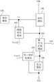
根据本发明的一方面,提供了一种像素驱动电路,像素驱动电路包括:储能模块、驱动模块、阈值补偿模块、第一初始化模块、第一发光控制模块和发光模块;According to an aspect of the present invention, a pixel driving circuit is provided, the pixel driving circuit includes: an energy storage module, a driving module, a threshold compensation module, a first initialization module, a first lighting control module, and a lighting module;
所述第一初始化模块与所述发光模块的第一端连接,所述阈值补偿模块的第一端与所述第一发光控制模块的第一端连接,所述第一发光控制模块的第二端与所述发光模块的第一端连接,所述阈值补偿模块的第二端与所述驱动模块的控制端连接;所述第一初始化模块用于在初始化阶段,输出初始化信号,所述阈值补偿模块和所述第一发光控制模块用于在所述初始化阶段导通,将所述初始化信号发送至所述驱动模块的控制端;The first initialization module is connected to the first end of the light emitting module, the first end of the threshold compensation module is connected to the first end of the first light emitting control module, and the second end of the first light emitting control module The terminal is connected to the first terminal of the light-emitting module, and the second terminal of the threshold compensation module is connected to the control terminal of the driving module; the first initialization module is used for outputting an initialization signal in the initialization stage, the threshold value The compensation module and the first lighting control module are configured to be turned on in the initialization stage, and send the initialization signal to the control terminal of the driving module;
所述储能模块的第一端与所述驱动模块的控制端电连接,用于维持所述驱动模块的控制端电压;The first end of the energy storage module is electrically connected to the control end of the drive module for maintaining the voltage of the control end of the drive module;
所述阈值补偿模块用于对所述驱动模块的阈值电压进行补偿;The threshold compensation module is used for compensating the threshold voltage of the driving module;
所述驱动模块用于在发光阶段产生驱动电流,并使所述发光模块响应所述驱动电流发光。The driving module is used for generating a driving current in the light-emitting stage, and making the light-emitting module emit light in response to the driving current.
通过利用第一初始化模块输出初始化信号,阈值补偿模块和第一发光控制模块将初始化信号发送至驱动模块的控制端,可以减少驱动模块的漏电途径,有利于提高显示面板的显示均一性。By using the first initialization module to output the initialization signal, and the threshold compensation module and the first lighting control module to send the initialization signal to the control terminal of the driving module, the leakage path of the driving module can be reduced and the display uniformity of the display panel can be improved.
可选地,像素驱动电路还包括第二初始化模块,所述第二初始化模块的控制端接入第一扫描信号,所述第二初始化模块的第一端接入第一电源信号,所述第二初始化模块的第二端与所述储能模块的第一端电连接;所述第二初始化模块用于在所述初始化阶段初始化所述储能模块。Optionally, the pixel driving circuit further includes a second initialization module, the control terminal of the second initialization module is connected to the first scan signal, the first terminal of the second initialization module is connected to the first power signal, and the first power supply signal is connected to the first terminal of the second initialization module. The second end of the second initialization module is electrically connected to the first end of the energy storage module; the second initialization module is used to initialize the energy storage module in the initialization stage.
采用第二初始化模块初始化储能模块,可以清除储能模块上一帧残留的电压信号,以便驱动模块可以更准确的产生驱动电流;第二初始化模块通过第一电源信号对储能模块进行初始化,可以减少初始化信号线的数量,达到简化版图的效果。Using the second initialization module to initialize the energy storage module can clear the residual voltage signal in the previous frame of the energy storage module, so that the driving module can generate the driving current more accurately; the second initialization module initializes the energy storage module through the first power supply signal, The number of initialization signal lines can be reduced to achieve the effect of simplifying the layout.
可选地,所述第一初始化模块的控制端接入第二扫描信号,所述第一初始化模块的第一端接入第一电源信号,所述第一初始化模块的第二端与所述发光模块的第一端电连接;Optionally, the control end of the first initialization module is connected to the second scan signal, the first end of the first initialization module is connected to the first power supply signal, and the second end of the first initialization module is connected to the the first end of the light-emitting module is electrically connected;
所述发光模块的第二端接入所述第一电源信号。The second end of the light-emitting module is connected to the first power signal.
第一初始化模块采用第一电源信号对发光模块和驱动模块进行初始化,可以进一步减少初始化信号线的数量,从而进一步简化版图。The first initialization module uses the first power signal to initialize the light-emitting module and the driving module, which can further reduce the number of initialization signal lines, thereby further simplifying the layout.
可选地,像素驱动电路还包括数据写入模块;Optionally, the pixel driving circuit further includes a data writing module;
所述数据写入模块的控制端接入第三扫描信号,所述数据写入模块的第一端接入数据电压信号,所述数据写入模块的第二端与所述储能模块的第二端电连接;所述数据写入模块用于通过所述储能模块将数据电压信号写入所述驱动模块的控制端。The control end of the data writing module is connected to the third scan signal, the first end of the data writing module is connected to the data voltage signal, and the second end of the data writing module is connected to the first end of the energy storage module. The two terminals are electrically connected; the data writing module is used for writing the data voltage signal into the control terminal of the driving module through the energy storage module.
数据写入模块通过储能模块将数据电压信号写入驱动模块,使得驱动模块可以根据数据电压信号产生相应的驱动电流,发光模块根据驱动电流就可以显示待显示亮度。The data writing module writes the data voltage signal into the driving module through the energy storage module, so that the driving module can generate corresponding driving current according to the data voltage signal, and the light emitting module can display the brightness to be displayed according to the driving current.
可选地,所述储能模块的第二端接入第二电源信号。Optionally, the second end of the energy storage module is connected to a second power signal.
可选地,像素驱动电路还包括数据写入模块;Optionally, the pixel driving circuit further includes a data writing module;
所述数据写入模块的控制端接入第三扫描信号,所述数据写入模块的第一端接入数据电压信号,所述数据写入模块的第二端与所述驱动模块的第一端电连接,所述数据写入模块用于将所述数据电压信号写入所述驱动模块的控制端。The control terminal of the data writing module is connected to the third scan signal, the first terminal of the data writing module is connected to the data voltage signal, and the second terminal of the data writing module is connected to the first terminal of the driving module. The terminal is electrically connected, and the data writing module is used for writing the data voltage signal into the control terminal of the driving module.
数据写入模块可以直接将数据电压信号写入驱动模块的第一端,使得驱动模块可以根据数据电压信号产生相应的驱动电流。The data writing module can directly write the data voltage signal to the first end of the driving module, so that the driving module can generate a corresponding driving current according to the data voltage signal.
可选地,所述驱动模块的第一端连接第二电源信号;Optionally, the first end of the drive module is connected to a second power supply signal;
所述第一发光控制模块的控制端接入第一使能信号,所述第一发光控制模块的第二端与所述发光模块的第一端电连接;The control terminal of the first lighting control module is connected to the first enabling signal, and the second terminal of the first lighting control module is electrically connected to the first terminal of the lighting module;
所述阈值补偿模块的控制端接入第二扫描信号。The control end of the threshold compensation module is connected to the second scan signal.
储能模块可以维持驱动模块的控制端电压,阈值补偿模块可以对驱动模块的阈值电压进行补偿,从而使得驱动模块可以产生稳定的驱动电流,使得发光模块稳定发光。The energy storage module can maintain the control terminal voltage of the driving module, and the threshold compensation module can compensate the threshold voltage of the driving module, so that the driving module can generate a stable driving current and the light-emitting module can emit light stably.
根据本发明的另一方面,提供了一种像素驱动电路的驱动方法,所述驱动方法用于驱动本发明任一实施例所述的像素驱动电路,所述驱动方法包括:According to another aspect of the present invention, a driving method for a pixel driving circuit is provided, the driving method is used for driving the pixel driving circuit according to any embodiment of the present invention, and the driving method includes:
在初始化阶段,第一初始化模块、阈值补偿模块和第一发光控制模块导通,所述第一初始化模块输出初始化信号,所述阈值补偿模块和所述第一发光控制模块将所述初始化信号发送至驱动模块的控制端;In the initialization stage, the first initialization module, the threshold compensation module and the first lighting control module are turned on, the first initialization module outputs an initialization signal, and the threshold compensation module and the first lighting control module send the initialization signal to the control terminal of the drive module;
在阈值补偿阶段,所述阈值补偿模块导通,所述阈值补偿模块抓取所述驱动模块的阈值电压至所述驱动模块的控制端;In the threshold compensation stage, the threshold compensation module is turned on, and the threshold compensation module grabs the threshold voltage of the driving module to the control terminal of the driving module;
在发光阶段,所述驱动模块和所述第一发光控制模块导通,所述驱动模块产生驱动电流,所述发光模块响应所述驱动电流发光。In the lighting stage, the driving module and the first lighting control module are turned on, the driving module generates a driving current, and the lighting module emits light in response to the driving current.
通过利用第一初始化模块经过阈值补偿模块和第一发光控制模块初始化驱动模块,可以减少驱动模块的漏电途径,有利于提高显示面板的显示均一性。By using the first initialization module to initialize the driving module through the threshold compensation module and the first lighting control module, the leakage path of the driving module can be reduced, which is beneficial to improve the display uniformity of the display panel.
可选地,所述像素驱动电路还包括第二初始化模块;所述第二初始化模块的控制端接入第一扫描信号,所述第二初始化模块的第一端接入第一电源信号,所述第二初始化模块的第二端与所述储能模块的第二端电连接;Optionally, the pixel driving circuit further includes a second initialization module; the control end of the second initialization module is connected to the first scan signal, and the first end of the second initialization module is connected to the first power supply signal, so the second end of the second initialization module is electrically connected to the second end of the energy storage module;
在所述初始化阶段,还包括:所述第二初始化模块导通,所述第二初始化模块初始化所述储能模块;In the initialization stage, the method further includes: the second initialization module is turned on, and the second initialization module initializes the energy storage module;
在所述发光阶段,还包括:所述第二初始化模块导通,所述第一电源信号通过所述第二初始化模块为所述储能模块充电。In the light-emitting stage, the method further includes: the second initialization module is turned on, and the first power signal charges the energy storage module through the second initialization module.
采用第二初始化模块初始化储能模块,可以清除储能模块在上一帧残留的电压信号,以便驱动模块可以更准确的产生驱动电流。Using the second initialization module to initialize the energy storage module can clear the residual voltage signal of the energy storage module in the previous frame, so that the driving module can generate the driving current more accurately.
根据本发明的另一方面,提供了一种显示面板,显示面板包括本发明任一实施例所述的像素驱动电路。According to another aspect of the present invention, there is provided a display panel including the pixel driving circuit according to any embodiment of the present invention.
本发明实施例的技术方案,通过第一初始化模块输出初始化信号,第一发光控制模块和阈值补偿模块将初始化信号发送至驱动模块的控制端,可以无需为驱动模块设置单独的初始化模块,即驱动模块的控制端无需连接初始化模块,从而减少了驱动模块的控制端的漏电路径,有效减小了驱动模块的漏电电流,可以保证驱动模块的控制端电压的稳定性,从而保证驱动模块产生稳定的驱动电流,使得发光模块可以稳定发光,达到了提高显示面板的显示均一性的效果。并且,阈值补偿模块可以抓取驱动模块的阈值电压至驱动模块的控制端,达到对驱动模块的补偿效果,可以进一步保证驱动模块的稳定性,有利于提高显示面板的显示均一性。本发明实施例的技术方案解决了像素驱动电路中驱动模块的漏电电流较大,导致显示面板显示亮度不均的问题,达到了减小驱动模块的漏电电流的效果,提高了显示面板的显示均一性。In the technical solution of the embodiment of the present invention, the first initialization module outputs an initialization signal, and the first lighting control module and the threshold compensation module send the initialization signal to the control terminal of the driving module, so that there is no need to set a separate initialization module for the driving module, that is, the driving The control terminal of the module does not need to be connected to the initialization module, thereby reducing the leakage path of the control terminal of the driving module, effectively reducing the leakage current of the driving module, and ensuring the stability of the control terminal voltage of the driving module, thereby ensuring that the driving module generates stable driving The current enables the light-emitting module to emit light stably, thereby achieving the effect of improving the display uniformity of the display panel. In addition, the threshold compensation module can capture the threshold voltage of the driving module to the control terminal of the driving module to achieve a compensation effect on the driving module, which can further ensure the stability of the driving module and is beneficial to improve the display uniformity of the display panel. The technical solutions of the embodiments of the present invention solve the problem that the leakage current of the driving module in the pixel driving circuit is relatively large, resulting in uneven display brightness of the display panel, achieve the effect of reducing the leakage current of the driving module, and improve the display uniformity of the display panel. sex.
应当理解,本部分所描述的内容并非旨在标识本发明的实施例的关键或重要特征,也不用于限制本发明的范围。本发明的其它特征将通过以下的说明书而变得容易理解。It should be understood that the content described in this section is not intended to identify key or critical features of the embodiments of the invention, nor is it intended to limit the scope of the invention. Other features of the present invention will become readily understood from the following description.
附图说明Description of drawings
为了更清楚地说明本发明实施例中的技术方案,下面将对实施例描述中所需要使用的附图作简单地介绍,显而易见地,下面描述中的附图仅仅是本发明的一些实施例,对于本领域普通技术人员来讲,在不付出创造性劳动的前提下,还可以根据这些附图获得其他的附图。In order to illustrate the technical solutions in the embodiments of the present invention more clearly, the following briefly introduces the accompanying drawings used in the description of the embodiments. Obviously, the accompanying drawings in the following description are only some embodiments of the present invention. For those of ordinary skill in the art, other drawings can also be obtained from these drawings without creative effort.
图1是本发明实施例提供的一种像素驱动电路的结构示意图;1 is a schematic structural diagram of a pixel driving circuit provided by an embodiment of the present invention;
图2是本发明实施例提供的又一种像素驱动电路的结构示意图;FIG. 2 is a schematic structural diagram of another pixel driving circuit provided by an embodiment of the present invention;
图3是本发明实施例提供的又一种像素驱动电路的结构示意图;3 is a schematic structural diagram of another pixel driving circuit provided by an embodiment of the present invention;
图4是本发明实施例提供的又一种像素驱动电路的结构示意图;4 is a schematic structural diagram of another pixel driving circuit provided by an embodiment of the present invention;
图5是本发明实施例提供的又一种像素驱动电路的结构示意图;5 is a schematic structural diagram of another pixel driving circuit provided by an embodiment of the present invention;
图6是本发明实施例提供的又一种像素驱动电路的结构示意图;6 is a schematic structural diagram of another pixel driving circuit provided by an embodiment of the present invention;
图7是本发明实施例提供的一种像素驱动电路的驱动方法的流程图;7 is a flowchart of a driving method of a pixel driving circuit provided by an embodiment of the present invention;
图8是本发明实施例提供的一种像素驱动电路对应的时序图;8 is a timing diagram corresponding to a pixel driving circuit provided by an embodiment of the present invention;
图9是本发明实施例提供的又一种像素驱动电路的驱动方法的流程图;9 is a flowchart of another driving method of a pixel driving circuit provided by an embodiment of the present invention;
图10是本发明实施例提供的又一种像素驱动电路对应的时序图;10 is a timing diagram corresponding to another pixel driving circuit provided by an embodiment of the present invention;
图11是本发明实施例提供的又一种像素驱动电路的驱动方法的流程图;11 is a flowchart of another driving method of a pixel driving circuit provided by an embodiment of the present invention;
图12是本发明实施例提供的又一种像素驱动电路对应的时序图;12 is a timing diagram corresponding to another pixel driving circuit provided by an embodiment of the present invention;
图13是本发明实施例提供的又一种像素驱动电路对应的时序图。FIG. 13 is a timing diagram corresponding to another pixel driving circuit provided by an embodiment of the present invention.
具体实施方式Detailed ways
为了使本技术领域的人员更好地理解本发明方案,下面将结合本发明实施例中的附图,对本发明实施例中的技术方案进行清楚、完整地描述,显然,所描述的实施例仅仅是本发明一部分的实施例,而不是全部的实施例。基于本发明中的实施例,本领域普通技术人员在没有做出创造性劳动前提下所获得的所有其他实施例,都应当属于本发明保护的范围。In order to make those skilled in the art better understand the solutions of the present invention, the technical solutions in the embodiments of the present invention will be clearly and completely described below with reference to the accompanying drawings in the embodiments of the present invention. Obviously, the described embodiments are only Embodiments are part of the present invention, but not all embodiments. Based on the embodiments of the present invention, all other embodiments obtained by persons of ordinary skill in the art without creative efforts shall fall within the protection scope of the present invention.
需要说明的是,本发明的说明书和权利要求书及上述附图中的术语“第一”、“第二”等是用于区别类似的对象,而不必用于描述特定的顺序或先后次序。应该理解这样使用的数据在适当情况下可以互换,以便这里描述的本发明的实施例能够以除了在这里图示或描述的那些以外的顺序实施。此外,术语“包括”及其任何变形,意图在于覆盖不排他的包含,例如,包含了一系列步骤或单元的过程、方法、系统、产品或设备不必限于清楚地列出的那些步骤或单元,而是可包括没有清楚地列出的或对于这些过程、方法、产品或设备固有的其它步骤或单元。It should be noted that the terms "first", "second" and the like in the description and claims of the present invention and the above drawings are used to distinguish similar objects, and are not necessarily used to describe a specific sequence or sequence. It is to be understood that the data so used may be interchanged under appropriate circumstances such that the embodiments of the invention described herein can be practiced in sequences other than those illustrated or described herein. Furthermore, the term "comprising" and any variations thereof are intended to cover non-exclusive inclusion, for example, a process, method, system, product or device comprising a series of steps or elements is not necessarily limited to those steps or elements expressly listed, Rather, other steps or units not expressly listed or inherent to the process, method, product or apparatus may be included.
正如背景技术中提到的现有的显示面板存在显示亮度不均的问题,申请人经过仔细研究发现,产生此技术问题的原因在于:在像素驱动电路的发光阶段,驱动晶体管的漏电路径较多,驱动晶体管会通过阈值补偿晶体管漏电,驱动晶体管还会通过驱动晶体管的初始化晶体管漏电,形成两条漏电路径,即使增加晶体管或设置漏电控制晶体管也无法根本性解决漏电,使得驱动晶体管的栅极电压不稳而影响显示效果,显示面板的显示亮度不均。As mentioned in the background art, the existing display panel has the problem of uneven display brightness. After careful research, the applicant found that the reason for this technical problem is that in the light-emitting stage of the pixel driving circuit, there are many leakage paths of the driving transistor. , the drive transistor will compensate for transistor leakage through the threshold value, and the drive transistor will also leak through the initialization transistor of the drive transistor, forming two leakage paths. The instability affects the display effect, and the display brightness of the display panel is uneven.
针对上述问题,本发明实施例提供了一种像素驱动电路,图1是本发明实施例提供的一种像素驱动电路的结构示意图,参考图1,像素驱动电路包括:储能模块101、驱动模块102、阈值补偿模块103、第一初始化模块104、第一发光控制模块105和发光模块106;第一初始化模块104与发光模块106的第一端连接,阈值补偿模块103的第一端与第一发光控制模块105的第一端连接,第一发光控制模块105的第二端与发光模块106的第一端连接,阈值补偿模块103的第二端与驱动模块102的控制端连接;第一初始化模块104用于在初始化阶段输出初始化信号,阈值补偿模块103和第一发光控制模块105用于在初始化阶段导通,将初始化信号发送至驱动模块102的控制端N1;储能模块101的第一端与驱动模块102的控制端电连接,用于维持驱动模块102的控制端N1电压;阈值补偿模块103用于对驱动模块102的阈值电压进行补偿;驱动模块102用于在发光阶段产生驱动电流,并使发光模块106响应驱动电流发光。In response to the above problems, an embodiment of the present invention provides a pixel driving circuit. FIG. 1 is a schematic structural diagram of a pixel driving circuit provided by an embodiment of the present invention. Referring to FIG. 1 , the pixel driving circuit includes: an
其中,驱动模块102可以根据数据电压信号产生相应的驱动电流,发光模块106例如为有机发光二极管(Organic Light-Emitting Diode,OLED),发光模块106可以响应驱动电流进行发光,以显示待显示亮度。The
具体地,在初始化阶段,第一初始化模块104可以初始化发光模块106,可以清除发光模块106上一帧的电压信号,以便发光模块106可以更好的根据驱动电流显示待显示亮度;并且第一初始化模块104可以输出初始化信号,第一发光控制模块105和阈值补偿模块103可以将初始化信号写入驱动模块102的控制端N1,利用第一初始化模块104初始化驱动模块102,可以无需为驱动模块102设置单独的初始化模块,即驱动模块102的控制端N1无需连接初始化模块,减少了驱动模块102的控制端N1经过初始化模块漏电的路径,从而减少了一条漏电路径,有效减小了驱动模块102的漏电电流,可以保证驱动模块102的控制端N1电压的稳定性,从而保证驱动模块102产生稳定的驱动电流,使得发光模块106可以稳定发光,达到了提高显示面板的显示均一性的效果。Specifically, in the initialization stage, the
并且,阈值补偿模块103可以抓取驱动模块102的阈值电压至驱动模块102的控制端N1,达到对驱动模块102的补偿效果,可以进一步保证驱动模块102的稳定性,有利于提高显示面板的显示均一性。In addition, the
此外,储能模块101可以维持驱动模块102的控制端N1的电压,在发光阶段,驱动模块102的控制端N1的电压可以更加稳定,可以进一步保证驱动模块102产生稳定的驱动电流,使得发光模块106更好的显示待显示亮度,进一步提高显示面板的显示均一性,改善显示面板的显示效果。In addition, the
本实施例的技术方案,通过第一初始化模块输出初始化信号,第一发光控制模块和阈值补偿模块将初始化信号发送至驱动模块的控制端,可以无需为驱动模块设置单独的初始化模块,即驱动模块的控制端无需连接初始化模块,从而减少了驱动模块的控制端的漏电路径,有效减小了驱动模块的漏电电流,可以保证驱动模块的控制端电压的稳定性,从而保证驱动模块产生稳定的驱动电流,使得发光模块可以稳定发光,达到了提高显示面板的显示均一性的效果。并且,阈值补偿模块可以抓取驱动模块的阈值电压至驱动模块的控制端,达到对驱动模块的补偿效果,可以进一步保证驱动模块的稳定性,有利于提高显示面板的显示均一性。本实施例的技术方案解决了像素驱动电路中驱动模块的漏电电流较大,导致显示面板显示亮度不均的问题,达到了减小驱动模块的漏电电流的效果,提高了显示面板的显示均一性。In the technical solution of this embodiment, the first initialization module outputs an initialization signal, and the first lighting control module and the threshold compensation module send the initialization signal to the control terminal of the driving module, so that there is no need to set a separate initialization module for the driving module, that is, the driving module The control terminal does not need to be connected to the initialization module, thus reducing the leakage path of the control terminal of the driving module, effectively reducing the leakage current of the driving module, and ensuring the stability of the control terminal voltage of the driving module, thereby ensuring that the driving module generates a stable driving current , so that the light-emitting module can emit light stably, and the effect of improving the display uniformity of the display panel is achieved. In addition, the threshold compensation module can capture the threshold voltage of the driving module to the control terminal of the driving module to achieve a compensation effect on the driving module, which can further ensure the stability of the driving module and is beneficial to improve the display uniformity of the display panel. The technical solution of this embodiment solves the problem that the leakage current of the driving module in the pixel driving circuit is relatively large, resulting in uneven display brightness of the display panel, achieves the effect of reducing the leakage current of the driving module, and improves the display uniformity of the display panel .
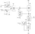
图2是本发明实施例提供的又一种像素驱动电路的结构示意图,可选地,参考图2,像素驱动电路还包括第二初始化模块107,与储能模块101电连接;第二初始化模块107用于在初始化阶段初始化储能模块101。FIG. 2 is a schematic structural diagram of another pixel driving circuit provided by an embodiment of the present invention. Optionally, referring to FIG. 2, the pixel driving circuit further includes a
具体地,第二初始化模块107可以在初始化阶段初始化储能模块101,可以清除储能模块101在上一帧残留的电压信号,使得储能模块101可以更好的稳定驱动模块102的控制端N1的电压,以便驱动模块102可以更准确的产生驱动电流。Specifically, the
可选地,继续参考图2,第二初始化模块107的控制端接入第一扫描信号Scan1,第二初始化模块107的第一端接入第一电源信号VSS,第二初始化模块107的第二端与储能模块101的第二端电连接。Optionally, continue to refer to FIG. 2 , the control terminal of the
具体地,第一电源信号VSS例如为负电压信号,第二初始化模块107的第一端接入第一电源信号VSS,第二初始化模块107在初始化阶段将第一电源信号VSS写入储能模块101的第二端,即第二初始化模块107采用第一电源信号VSS对储能模块101进行初始化,将第一电源信号VSS作为初始化信号,使得第二初始化模块107无需额外接入初始化信号,节省了初始化信号线,有利于简化显示面板的版图。Specifically, the first power supply signal VSS is, for example, a negative voltage signal, the first end of the
可选地,继续参考图2,第一初始化模块104的控制端接入第二扫描信号Scan2,第一初始化模块104的第一端接入第一电源信号VSS,第一初始化模块104的第二端与发光模块106的第一端电连接;发光模块106的第二端接入第一电源信号VSS。Optionally, continue referring to FIG. 2 , the control terminal of the
具体地,第二扫描信号Scan2可以控制第一初始化模块104导通或关断,第一初始化模块104可以将第一电源信号VSS写入发光模块106的第一端,从而采用第一电源信号VSS对发光模块106进行初始化,并且可以采用第一电源信号VSS对驱动模块102的控制端N1进行初始化,第一电源信号VSS为发光模块106接入的电源信号,直接采用第一电源信号VSS对发光模块106和驱动模块102进行初始化。相比于相关技术中的采用Vref信号对驱动模块102的控制端进行初始化,本申请实施例复用发光模块106的第二端接入的第一电源信号VSS来对驱动模块102的控制端进行初始化,不需要Vref信号,减少了信号线的数量,有利于简化显示面板的版图。Specifically, the second scan signal Scan2 can control the
可选地,继续参考图2,像素驱动电路还包括数据写入模块108;数据写入模块108的控制端接入第三扫描信号Scan3,数据写入模块108的第一端接入数据电压信号Vdata,数据写入模块108的第二端与储能模块101的第二端电连接;数据写入模块108用于通过储能模块101将数据电压信号Vdata写入驱动模块102的控制端。Optionally, continuing to refer to FIG. 2 , the pixel driving circuit further includes a
具体地,第三扫描信号Scan3可以控制数据写入模块108的导通和关断,第三扫描信号Scan3控制数据写入模块108导通时,数据写入模块108可以将数据电压信号Vdata写入储能模块101,储能模块101可以将数据电压信号Vdata耦合至驱动模块102的控制端N1,从而使得驱动模块102可以根据数据电压信号Vdata产生相应的驱动电流,发光模块106就可以相应驱动电流发光,显示待显示亮度。Specifically, the third scan signal Scan3 can control the
可选地,参考图1或图2,驱动模块102的第一端连接第二电源信号VDD,驱动模块102的第二端与第一发光控制模块105的第一端电连接;第一发光控制模块105的控制端接入第一使能信号EM1;阈值补偿模块103的控制端接入第二扫描信号Scan2。Optionally, referring to FIG. 1 or FIG. 2 , the first terminal of the
具体地,第二电源信号VDD例如为正电压信号,储能模块101的第一端与驱动模块102的控制端N1电连接,储能模块101可以维持驱动模块102的控制端N1的电位,保证驱动模块102的稳定性,阈值补偿模块103可以抓取驱动模块102的阈值电压至驱动模块102的控制端N1,达到补偿驱动模块102的阈值电压的效果,进一步保证驱动模块102的稳定性,使得驱动模块102可以产生稳定的驱动电流,保证了显示面板的显示亮度均一性。Specifically, the second power signal VDD is, for example, a positive voltage signal, the first terminal of the
在上述实施方案的基础上,图3是本发明实施例提供的又一种像素驱动电路的结构示意图,可选地,参考图3,像素驱动电路还包括第二发光控制模块109,第二发光控制模块109的控制端接入第二使能信号EM2,第二发光控制模块109的第一端接入第二电源信号VDD,第二发光控制模块109的第二端与驱动模块102的第一端N2电连接。On the basis of the above embodiment, FIG. 3 is a schematic structural diagram of another pixel driving circuit provided by an embodiment of the present invention. Optionally, referring to FIG. The control terminal of the
图4是本发明实施例提供的又一种像素驱动电路的结构示意图,可选地,参考图4,像素驱动电路还包括数据写入模块108;数据写入模块108的控制端接入第三扫描信号Scan3,数据写入模块108的第一端接入数据电压信号Vdata,数据写入模块108的第二端与驱动模块102的第一端N2电连接,数据写入模块108用于将数据电压信号Vdata写入驱动模块102。FIG. 4 is a schematic structural diagram of another pixel driving circuit provided by an embodiment of the present invention. Optionally, referring to FIG. 4 , the pixel driving circuit further includes a
具体地,数据写入模块108可以直接与驱动模块102的第一端N2电连接,即数据写入模块108可以直接将数据电压信号Vdata写入驱动模块102的第一端,使得驱动模块102可以根据数据电压信号Vdata产生相应的驱动电流。Specifically, the
或者,图5是本发明实施例提供的又一种像素驱动电路的结构示意图,可选地,参考图5,储能模块101的第二端接入第二电源信号VDD。Alternatively, FIG. 5 is a schematic structural diagram of another pixel driving circuit provided by an embodiment of the present invention. Optionally, referring to FIG. 5 , the second end of the
具体地,参考图5,驱动模块102的控制端N1未连接初始化模块,第一初始化模块104可以经过第一发光控制模块105和阈值补偿模块103为驱动模块102的控制端N1进行初始化,使得驱动模块102的漏电路径减少,有效减小了驱动模块102的漏电电流,可以保证驱动模块102的控制端N1电压的稳定性。Specifically, referring to FIG. 5 , the control terminal N1 of the
图6是本发明实施例提供的又一种像素驱动电路的结构示意图,可选地,参考图6,储能模块101包括电容C1,电容C1的第一端为储能模块101的第一端,电容C1的第二端为储能模块101的第二端;驱动模块102包括驱动晶体管T1,驱动晶体管T1的控制端为驱动模块102的控制端N1,驱动晶体管T1的第一端为驱动模块102的第一端N2,驱动晶体管T1的第二端为驱动模块102的第二端;阈值补偿模块103包括第一晶体管T2,第一晶体管T2的控制端为阈值补偿模块103的控制端,第一晶体管T2的第一端为阈值补偿模块103的第一端,第一晶体管T2的第二端为阈值补偿模块103的第二端;第一初始化模块104包括第二晶体管T3,第二晶体管T3的控制端为第一初始化模块104的控制端,第二晶体管T3的第一端为第一初始化模块104的第一端,第二晶体管T3的第二端为第一初始化模块104的第二端;第一发光控制模块105包括第三晶体管T4,第三晶体管T4的控制端为第一发光控制模块105的控制端,第三晶体管T4的第一端为第一发光控制模块105的第一端,第三晶体管T4的第二端为第一发光控制模块105的第二端;发光模块106包括发光二极管D1,发光二极管D1的阳极为发光模块106的第一端,发光二极管D1的阴极为发光模块106的第二端;第二初始化模块107包括第四晶体管T5,第四晶体管T5的控制端为第二初始化模块107的控制端,第四晶体管T5的第一端为第二初始化模块107的第一端,第四晶体管T5的第二端为第二初始化模块107的第二端;数据写入模块108包括第五晶体管T6,第五晶体管T6的控制端为数据写入模块108的控制端,第五晶体管T6的第一端为数据写入模块108的第一端,第五晶体管T6的第二端为数据写入模块108的第二端;第二发光控制模块109包括第六晶体管T7,第六晶体管T7的控制端为第二发光控制模块109的控制端,第六晶体管T7的第一端为第二发光控制模块109的第一端,第六晶体管T7的第二端为第二发光控制模块109的第二端。FIG. 6 is a schematic structural diagram of another pixel driving circuit provided by an embodiment of the present invention. Optionally, referring to FIG. 6 , the energy storage module 101 includes a capacitor C1 , and the first end of the capacitor C1 is the first end of the energy storage module 101 , the second end of the capacitor C1 is the second end of the energy storage module 101; the drive module 102 includes a drive transistor T1, the control end of the drive transistor T1 is the control end N1 of the drive module 102, and the first end of the drive transistor T1 is the drive module The first end N2 of 102, the second end of the driving transistor T1 is the second end of the driving module 102; the threshold compensation module 103 includes a first transistor T2, and the control end of the first transistor T2 is the control end of the threshold compensation module 103, the first The first end of a transistor T2 is the first end of the threshold compensation module 103, the second end of the first transistor T2 is the second end of the threshold compensation module 103; the first initialization module 104 includes a second transistor T3, the second transistor T3 The control end of the second transistor T3 is the control end of the first initialization module 104 , the first end of the second transistor T3 is the first end of the first initialization module 104 , and the second end of the second transistor T3 is the second end of the first initialization module 104 The first light-emitting control module 105 includes a third transistor T4, the control end of the third transistor T4 is the control end of the first light-emitting control module 105, and the first end of the third transistor T4 is the first end of the first light-emitting control module 105 , the second end of the third transistor T4 is the second end of the first light-emitting control module 105; the light-emitting module 106 includes a light-emitting diode D1, the anode of the light-emitting diode D1 is the first end of the light-emitting module 106, and the cathode of the light-emitting diode D1 is light-emitting The second end of the module 106; the second initialization module 107 includes a fourth transistor T5, the control end of the fourth transistor T5 is the control end of the second initialization module 107, and the first end of the fourth transistor T5 is the second initialization module 107 The first end, the second end of the fourth transistor T5 is the second end of the second initialization module 107; the data writing module 108 includes a fifth transistor T6, and the control end of the fifth transistor T6 is the control end of the data writing module 108 , the first end of the fifth transistor T6 is the first end of the data writing module 108, the second end of the fifth transistor T6 is the second end of the data writing module 108; the second lighting control module 109 includes the sixth transistor T7 , the control terminal of the sixth transistor T7 is the control terminal of the second lighting control module 109, the first terminal of the sixth transistor T7 is the first terminal of the second lighting control module 109, and the second terminal of the sixth transistor T7 is the second terminal of the second lighting control module 109. The second end of the
需要说明的是,图6中只示出了各个晶体管为P型晶体管的情况,但并不进行限定,各个晶体管的具体类型可以根据实际情况进行确定,本实施例并不进行限定。It should be noted that FIG. 6 only shows the case where each transistor is a P-type transistor, but it is not limited. The specific type of each transistor can be determined according to the actual situation, which is not limited in this embodiment.
图7是本发明实施例提供的一种像素驱动电路的驱动方法的流程图,参考图7,驱动方法用于驱动上述任意实施方案提供的像素驱动电路,驱动方法包括:7 is a flowchart of a driving method of a pixel driving circuit provided by an embodiment of the present invention. Referring to FIG. 7 , the driving method is used to drive the pixel driving circuit provided by any of the above embodiments, and the driving method includes:
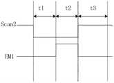
S610、在初始化阶段,第一初始化模块、阈值补偿模块和第一发光控制模块导通,第一初始化模块输出初始化信号,阈值补偿模块和第一发光控制模块将初始化信号发送至驱动模块的控制端。S610. In the initialization stage, the first initialization module, the threshold compensation module and the first lighting control module are turned on, the first initialization module outputs an initialization signal, and the threshold compensation module and the first lighting control module send the initialization signal to the control terminal of the driving module .
具体地,图8是本发明实施例提供的一种像素驱动电路对应的时序图,参考图8和图1,在初始化阶段t1,第二扫描信号Scan2为低电平,第一初始化模块104和阈值补偿模块103导通,第一使能信号EM1为低电平,第一发光控制模块105导通,第一初始化模块104可以将第一电源信号VSS写入发光模块106的第一端,初始化发光模块106;并且,第一初始化模块104可以将第一电源信号VSS输出,第一发光控制模块105和阈值补偿模块103可以将第一电源信号VSS写入驱动模块102的控制端N1,初始化驱动模块102。利用第一初始化模块104初始化驱动模块102,可以无需为驱动模块102设置单独的初始化模块,即驱动模块102的控制端N1无需连接初始化模块,从而减少了驱动模块102的控制端N1的漏电路径,有效减小了驱动模块102的漏电电流,可以保证驱动模块102的控制端N1电压的稳定性,从而保证驱动模块102产生稳定的驱动电流,使得发光模块106可以稳定发光,达到了提高显示面板的显示均一性的效果。Specifically, FIG. 8 is a timing diagram corresponding to a pixel driving circuit provided by an embodiment of the present invention. Referring to FIG. 8 and FIG. 1 , in the initialization stage t1, the second scan signal Scan2 is at a low level, and the
S620、在阈值补偿阶段,阈值补偿模块导通,阈值补偿模块抓取驱动模块的阈值电压至驱动模块的控制端。S620. In the threshold compensation stage, the threshold compensation module is turned on, and the threshold compensation module grabs the threshold voltage of the driving module to the control terminal of the driving module.
具体地,参考图8和图1,在阈值补偿阶段t2,第二扫描信号Scan2为低电平,阈值补偿模块103导通,阈值补偿模块103可以抓取驱动模块102的阈值电压至驱动模块102的控制端N1,达到对驱动模块102的补偿效果,可以进一步保证驱动模块102的稳定性,有利于提高显示面板的显示均一性。Specifically, referring to FIG. 8 and FIG. 1 , in the threshold compensation stage t2 , the second scan signal Scan2 is at a low level, the
并且,第一初始化模块104导通,第一初始化模块104可以继续将第一电源信号VSS写入发光模块106的第一端,增加了对发光模块106初始化的时间,对发光模块106的第一端进行电荷累积作用的时间更长,可以达到更好的初始化效果。在其它一些实施方式中,也可以采用参考信号Vref作为初始化信号进行初始化。In addition, when the
S630、在发光阶段,驱动模块和第一发光控制模块导通,驱动模块产生驱动电流,发光模块响应驱动电流发光。S630. In the lighting stage, the driving module and the first lighting control module are turned on, the driving module generates a driving current, and the lighting module emits light in response to the driving current.
具体地,参考图8和图1,在发光阶段t3,第一使能信号EM1为低电平,驱动模块102和第一发光控制模块105导通,驱动模块102可以产生驱动电流,发光模块106响应驱动电流发光,显示待显示亮度。Specifically, referring to FIG. 8 and FIG. 1 , in the lighting stage t3, the first enable signal EM1 is at a low level, the
可选地,参考图2,像素驱动电路还包括第二初始化模块107,第二初始化模块107的控制端接入第一扫描信号Scan1,第二初始化模块107的第一端接入第一电源信号VSS,第二初始化模块107的第二端与储能模块101的第二端电连接。Optionally, referring to FIG. 2 , the pixel driving circuit further includes a
图9是本发明实施例提供的又一种像素驱动电路的驱动方法的流程图,可选地,参考图9,驱动方法用于驱动上述任意实施方案提供的像素驱动电路,驱动方法包括:FIG. 9 is a flowchart of another driving method for a pixel driving circuit provided by an embodiment of the present invention. Optionally, referring to FIG. 9 , the driving method is used to drive the pixel driving circuit provided by any of the above embodiments, and the driving method includes:
S710、在初始化阶段,第一初始化模块、阈值补偿模块、第一发光控制模块和第二初始化模块导通,第一初始化模块输出初始化信号,阈值补偿模块和第一发光控制模块将初始化信号发送至驱动模块的控制端;第二初始化模块初始化储能模块。S710. In the initialization stage, the first initialization module, the threshold compensation module, the first lighting control module and the second initialization module are turned on, the first initialization module outputs an initialization signal, and the threshold compensation module and the first lighting control module send the initialization signal to The control terminal of the drive module; the second initialization module initializes the energy storage module.
具体地,图10是本发明实施例提供的又一种像素驱动电路对应的时序图,参考图10和图2,在初始化阶段t1,第一扫描信号Scan1为低电平,第二初始化模块107导通,第二初始化模块107初始化储能模块101;第二扫描信号Scan2为低电平,第一初始化模块104和阈值补偿模块103导通,第一使能信号EM1为低电平,第一发光控制模块105导通,第一初始化模块104初始化发光模块106和驱动模块102。Specifically, FIG. 10 is a timing diagram corresponding to another pixel driving circuit provided by an embodiment of the present invention. Referring to FIG. 10 and FIG. 2 , in the initialization stage t1, the first scan signal Scan1 is at a low level, and the
S720、在阈值补偿阶段,阈值补偿模块导通,阈值补偿模块抓取驱动模块的阈值电压至驱动模块的控制端。S720. In the threshold compensation stage, the threshold compensation module is turned on, and the threshold compensation module grabs the threshold voltage of the driving module to the control terminal of the driving module.
S730、在发光阶段,第二初始化模块、驱动模块和第一发光控制模块导通,第一电源信号通过第二初始化模块为储能模块充电;驱动模块产生驱动电流,发光模块响应驱动电流发光。S730. In the lighting stage, the second initialization module, the driving module and the first lighting control module are turned on, and the first power signal charges the energy storage module through the second initialization module; the driving module generates a driving current, and the lighting module emits light in response to the driving current.
具体地,参考图10和图2,在发光阶段t3,第一扫描信号Scan1为低电平,第二初始化模块107导通,第二初始化模块107将第一电源信号VSS写入储能模块101;第一使能信号EM1为低电平,驱动模块102和第一发光控制模块105导通,驱动模块102可以产生驱动电流,发光模块106响应驱动电流发光,显示待显示亮度。Specifically, referring to FIG. 10 and FIG. 2 , in the light-emitting stage t3, the first scan signal Scan1 is at a low level, the
可选地,参考图3,像素驱动电路还包括第二初始化模块107、数据写入模块108和第二发光控制模块109;第二初始化模块107的控制端接入第一扫描信号Scan1,第二初始化模块107的第一端接入第一电源信号VSS,第二初始化模块107的第二端与储能模块101的第二端电连接;数据写入模块108的控制端接入第三扫描信号Scan3,数据写入模块108的第一端接入数据电压信号Vdata,数据写入模块108的第二端与储能模块101的第二端电连接;第二发光控制模块109的控制端接入第二使能信号EM2,第二发光控制模块109的第一端接入第二电源信号VDD,第二发光控制模块109的第二端与驱动模块102的第一端N2电连接。Optionally, referring to FIG. 3 , the pixel driving circuit further includes a
图11是本发明实施例提供的又一种像素驱动电路的驱动方法的流程图,可选地,参考图11,驱动方法用于驱动上述任意实施方案提供的像素驱动电路,驱动方法包括:11 is a flowchart of another driving method for a pixel driving circuit provided by an embodiment of the present invention. Optionally, referring to FIG. 11 , the driving method is used to drive the pixel driving circuit provided by any of the above embodiments, and the driving method includes:
S810、在初始化阶段,第一初始化模块、阈值补偿模块、第一发光控制模块和第二初始化模块导通,第一初始化模块输出初始化信号,阈值补偿模块和第一发光控制模块将初始化信号发送至驱动模块的控制端;第二初始化模块初始化储能模块。S810. In the initialization stage, the first initialization module, the threshold compensation module, the first lighting control module and the second initialization module are turned on, the first initialization module outputs an initialization signal, and the threshold compensation module and the first lighting control module send the initialization signal to The control terminal of the drive module; the second initialization module initializes the energy storage module.
S820、在阈值补偿阶段,阈值补偿模块、第一初始化模块、第二发光控制模块、驱动模块和数据电压写入模块导通,阈值补偿模块抓取驱动模块的阈值电压至驱动模块的控制端;数据写入模块将数据电压信号写入储能模块的第二端;第二电源信号经过第二发光控制模块和阈值补偿模块为储能模块的第一端充电。S820, in the threshold compensation stage, the threshold compensation module, the first initialization module, the second lighting control module, the driving module and the data voltage writing module are turned on, and the threshold compensation module grabs the threshold voltage of the driving module to the control end of the driving module; The data writing module writes the data voltage signal into the second end of the energy storage module; the second power signal charges the first end of the energy storage module through the second lighting control module and the threshold compensation module.
具体地,图12是本发明实施例提供的又一种像素驱动电路对应的时序图,参考图12和图3,在阈值补偿阶段t2,第二使能信号EM2、第二扫描信号Scan2和第三扫描信号Scan3为低电平,第二发光控制模块109、阈值补偿模块103、第一初始化模块104和数据写入模块108导通;第二电源信号VDD经过第二发光控制模块109、驱动模块102和阈值补偿模块103为储能模块101的第一端充电,则储能模块101的第一端的电压为VDD-Vth,即驱动模块102的控制端N1的电压为VDD-Vth。Specifically, FIG. 12 is a timing diagram corresponding to another pixel driving circuit provided by an embodiment of the present invention. Referring to FIG. 12 and FIG. 3 , in the threshold compensation stage t2, the second enable signal EM2, the second scan signal Scan2 and the first The third scan signal Scan3 is at low level, the second
数据写入模块108将数据电压信号Vdata写入到储能模块101的第二端,则储能模块101的第二端的电压为Vdata。The
初始化信号S830、在发光阶段,第二初始化模块、驱动模块、第一发光控制模块和第二发光控制模块导通,第一电源信号通过第二初始化模块为储能模块充电;驱动模块产生驱动电流,发光模块响应驱动电流发光。Initialization signal S830: In the lighting stage, the second initialization module, the driving module, the first lighting control module and the second lighting control module are turned on, and the first power signal charges the energy storage module through the second initialization module; the driving module generates a driving current , the light emitting module emits light in response to the driving current.
具体地,参考图12和图3,在发光阶段t3,第一扫描信号Scan1为低电平,第二初始化模块107导通,第二初始化模块107将第一电源信号VSS写入储能模块101,则驱动模块102的控制端N1的电压为VDD-Vth+VSS-Vdata;第一使能信号EM1和第二使能信号EM2为低电平,第一发光控制模块105和第二发光控制模块109导通,驱动模块102导通,驱动模块102产生驱动电流,发光模块106响应驱动电流发光,在正常发光时,通过驱动模块102的驱动电流I=K(Vgs-Vth)2=K(VDD-VDD+Vth-VSS+Vdata-Vth)2=K(Vdata-VSS)2,则驱动电流只与数据电压信号Vdata和第一电源信号VSS有关,与阈值电压无关,可以保证驱动电流的稳定性,有利于改善显示面板的显示效果,提高显示均一性。Specifically, referring to FIG. 12 and FIG. 3 , in the light-emitting stage t3, the first scan signal Scan1 is at a low level, the
示例性的,参考图4和图12,在初始化阶段t1,第一扫描信号Scan1为低电平,第二初始化模块107导通,第二初始化模块107初始化储能模块101;第二扫描信号Scan2为低电平,第一初始化模块104和阈值补偿模块103导通,第一初始化模块104初始化发光模块106和驱动模块102;在阈值补偿阶段t2,数据写入模块108导通,数据写入模块108可将数据电压信号Vdata写入驱动模块102的第一端N2,则驱动模块102的第一端N2的电压为Vdata,且阈值补偿模块103导通,则驱动模块102的控制端N1的电压为Vdata-Vth;在发光阶段t3,第二初始化模块107导通,第二初始化模块107将第一电源信号VSS写入储能模块101,则驱动模块102的控制端N1的电压为Vdata-Vth+VSS,则在正常发光时,通过驱动模块102的驱动电流I=K(Vgs-Vth)2=K(VDD-Vdata+Vth-VSS-Vth)2=K(VDD-Vdata-VSS)2,则驱动电流只与数据电压信号Vdata、第一电源信号VSS和第二电源信号VDD有关,与阈值电压无关,可以保证驱动电流的稳定性,有利于改善显示面板的显示效果,提高显示均一性。4 and 12, in the initialization stage t1, the first scan signal Scan1 is at a low level, the second initialization module 107 is turned on, the second initialization module 107 initializes the energy storage module 101; the second scan signal Scan2 When the level is low, the first initialization module 104 and the threshold compensation module 103 are turned on, and the first initialization module 104 initializes the light-emitting module 106 and the driving module 102; in the threshold compensation stage t2, the data writing module 108 is turned on, and the data writing module 108 can write the data voltage signal Vdata into the first terminal N2 of the driving module 102, then the voltage of the first terminal N2 of the driving module 102 is Vdata, and the threshold compensation module 103 is turned on, then the voltage of the control terminal N1 of the driving module 102 is is Vdata-Vth; in the light-emitting stage t3, the second initialization module 107 is turned on, the second initialization module 107 writes the first power supply signal VSS into the energy storage module 101, and the voltage of the control terminal N1 of the driving module 102 is Vdata-Vth +VSS, then during normal light emission, the driving current I=K(Vgs-Vth)2 =K(VDD-Vdata+Vth-VSS-Vth)2 =K(VDD-Vdata-VSS)2 through the driving module 102 , The driving current is only related to the data voltage signal Vdata, the first power supply signal VSS and the second power supply signal VDD, and has nothing to do with the threshold voltage, which can ensure the stability of the driving current, improve the display effect of the display panel, and improve the display uniformity.
示例性的,图13是本发明实施例提供的又一种像素驱动电路对应的时序图,参考图5和图13,在初始化阶段t1,第二扫描信号Scan2为低电平,第一初始化模块104和阈值补偿模块103导通,第一使能信号EM1为低电平,第一发光控制模块105导通,第一初始化模块104初始化发光模块106和驱动模块102;在阈值补偿阶段t2,数据写入模块108导通,数据写入模块108可将数据电压信号Vdata写入驱动模块102的第一端N2,则驱动模块102的第一端N2的电压为Vdata,且阈值补偿模块103导通,则驱动模块102的控制端N1的电压为Vdata-Vth;在发光阶段t3,驱动模块102的控制端N1的电压为Vdata-Vth,则在正常发光时,通过驱动模块102的驱动电流I=K(Vgs-Vth)2=K(VDD-Vdata+Vth-Vth)2=K(VDD-Vdata)2,则驱动电流只与数据电压信号Vdata和第二电源信号VDD有关,与阈值电压无关,可以保证驱动电流的稳定性,有利于改善显示面板的显示效果,提高显示均一性。Exemplarily, FIG. 13 is a timing diagram corresponding to another pixel driving circuit provided by an embodiment of the present invention. Referring to FIG. 5 and FIG. 13 , in the initialization stage t1, the second scan signal Scan2 is at a low level, and the first initialization module 104 and the threshold compensation module 103 are turned on, the first enable signal EM1 is low level, the first lighting control module 105 is turned on, the first initialization module 104 initializes the lighting module 106 and the driving module 102; in the threshold compensation stage t2, the data The writing module 108 is turned on, the data writing module 108 can write the data voltage signal Vdata into the first terminal N2 of the driving module 102, the voltage of the first terminal N2 of the driving module 102 is Vdata, and the threshold compensation module 103 is turned on , the voltage of the control terminal N1 of the driving module 102 is Vdata-Vth; in the light-emitting stage t3, the voltage of the control terminal N1 of the driving module 102 is Vdata-Vth, then during normal lighting, the driving current I = K(Vgs-Vth)2 =K(VDD-Vdata+Vth-Vth)2 =K(VDD-Vdata)2 , then the driving current is only related to the data voltage signal Vdata and the second power supply signal VDD, and has nothing to do with the threshold voltage, The stability of the driving current can be ensured, which is beneficial to improving the display effect of the display panel and improving the display uniformity.
需要说明的是,图8、图10、图12和图13的时序图只示出了各个模块为低电平导通的情况,在其它一些实施方式中,各个模块也可以为高电平导通,具体的导通条件可以根据实际情况进行确定,本实施例并不进行限定。It should be noted that the timing diagrams in FIG. 8 , FIG. 10 , FIG. 12 , and FIG. 13 only show the case where each module is turned on at a low level. In other embodiments, each module can also be turned on at a high level. The specific conduction condition can be determined according to the actual situation, which is not limited in this embodiment.
本发明实施例还提供了一种显示面板,该显示面板包括上述任意实施方案提供的像素驱动电路,显示面板的实现原理和技术效果与像素驱动电路的实现原理和技术效果类似,此处不再赘述。The embodiment of the present invention also provides a display panel, the display panel includes the pixel driving circuit provided by any of the above-mentioned embodiments, the realization principle and technical effect of the display panel are similar to those of the pixel driving circuit, and are not repeated here. Repeat.
应该理解,可以使用上面所示的各种形式的流程,重新排序、增加或删除步骤。例如,本发明中记载的各步骤可以并行地执行也可以顺序地执行也可以不同的次序执行,只要能够实现本发明的技术方案所期望的结果,本文在此不进行限制。It should be understood that steps may be reordered, added or deleted using the various forms of flow shown above. For example, the steps described in the present invention can be performed in parallel, sequentially or in different orders, and as long as the desired results of the technical solutions of the present invention can be achieved, no limitation is imposed herein.
上述具体实施方式,并不构成对本发明保护范围的限制。本领域技术人员应该明白的是,根据设计要求和其他因素,可以进行各种修改、组合、子组合和替代。任何在本发明的精神和原则之内所作的修改、等同替换和改进等,均应包含在本发明保护范围之内。The above-mentioned specific embodiments do not constitute a limitation on the protection scope of the present invention. It should be understood by those skilled in the art that various modifications, combinations, sub-combinations and substitutions may occur depending on design requirements and other factors. Any modifications, equivalent replacements and improvements made within the spirit and principle of the present invention shall be included within the protection scope of the present invention.
Claims (10)
Translated fromChinesePriority Applications (1)
| Application Number | Priority Date | Filing Date | Title |
|---|---|---|---|
| CN202210351704.8ACN114743491A (en) | 2022-04-02 | 2022-04-02 | Pixel driving circuit, driving method thereof and display panel |
Applications Claiming Priority (1)
| Application Number | Priority Date | Filing Date | Title |
|---|---|---|---|
| CN202210351704.8ACN114743491A (en) | 2022-04-02 | 2022-04-02 | Pixel driving circuit, driving method thereof and display panel |
Publications (1)
| Publication Number | Publication Date |
|---|---|
| CN114743491Atrue CN114743491A (en) | 2022-07-12 |
Family
ID=82279288
Family Applications (1)
| Application Number | Title | Priority Date | Filing Date |
|---|---|---|---|
| CN202210351704.8APendingCN114743491A (en) | 2022-04-02 | 2022-04-02 | Pixel driving circuit, driving method thereof and display panel |
Country Status (1)
| Country | Link |
|---|---|
| CN (1) | CN114743491A (en) |
Cited By (4)
| Publication number | Priority date | Publication date | Assignee | Title |
|---|---|---|---|---|
| CN115512656A (en)* | 2022-10-31 | 2022-12-23 | 云谷(固安)科技有限公司 | Pixel circuit, driving method thereof and display panel |
| CN116153253A (en)* | 2023-03-08 | 2023-05-23 | 厦门天马显示科技有限公司 | Display panel, driving circuit and display device |
| CN118609513A (en)* | 2024-08-09 | 2024-09-06 | 惠科股份有限公司 | Pixel driving circuit, pixel driving method and display panel |
| CN119600943A (en)* | 2025-01-16 | 2025-03-11 | 北京维信诺科技有限公司 | Pixel circuit and driving method thereof, and display panel |
Citations (12)
| Publication number | Priority date | Publication date | Assignee | Title |
|---|---|---|---|---|
| CN103971640A (en)* | 2014-05-07 | 2014-08-06 | 京东方科技集团股份有限公司 | Pixel driving circuit, driving method of pixel driving circuit and display device |
| CN104809989A (en)* | 2015-05-22 | 2015-07-29 | 京东方科技集团股份有限公司 | Pixel circuit, drive method thereof and related device |
| CN106097964A (en)* | 2016-08-22 | 2016-11-09 | 京东方科技集团股份有限公司 | Image element circuit, display floater, display device and driving method |
| CN106531076A (en)* | 2017-01-12 | 2017-03-22 | 京东方科技集团股份有限公司 | Pixel circuit, display panel and driving method thereof |
| CN107038997A (en)* | 2017-05-26 | 2017-08-11 | 京东方科技集团股份有限公司 | Image element circuit, image element driving method and display device |
| CN109493794A (en)* | 2019-01-24 | 2019-03-19 | 鄂尔多斯市源盛光电有限责任公司 | Pixel circuit, image element driving method and display device |
| CN109493795A (en)* | 2019-01-25 | 2019-03-19 | 鄂尔多斯市源盛光电有限责任公司 | Pixel circuit, image element driving method and display device |
| CN111986612A (en)* | 2020-08-31 | 2020-11-24 | 云谷(固安)科技有限公司 | Pixel driving circuit, driving method of pixel driving circuit and display panel |
| CN113674690A (en)* | 2021-08-25 | 2021-11-19 | 合肥维信诺科技有限公司 | Pixel driving circuit, display panel, display device and driving method |
| CN113808542A (en)* | 2021-09-22 | 2021-12-17 | 北京京东方技术开发有限公司 | Pixel circuit, driving method and display device |
| CN113808521A (en)* | 2021-09-22 | 2021-12-17 | 昆山国显光电有限公司 | Pixel circuit, display panel and driving method of pixel circuit |
| CN114255688A (en)* | 2021-12-23 | 2022-03-29 | 合肥维信诺科技有限公司 | Pixel circuit, driving method thereof and display panel |
- 2022
- 2022-04-02CNCN202210351704.8Apatent/CN114743491A/enactivePending
Patent Citations (12)
| Publication number | Priority date | Publication date | Assignee | Title |
|---|---|---|---|---|
| CN103971640A (en)* | 2014-05-07 | 2014-08-06 | 京东方科技集团股份有限公司 | Pixel driving circuit, driving method of pixel driving circuit and display device |
| CN104809989A (en)* | 2015-05-22 | 2015-07-29 | 京东方科技集团股份有限公司 | Pixel circuit, drive method thereof and related device |
| CN106097964A (en)* | 2016-08-22 | 2016-11-09 | 京东方科技集团股份有限公司 | Image element circuit, display floater, display device and driving method |
| CN106531076A (en)* | 2017-01-12 | 2017-03-22 | 京东方科技集团股份有限公司 | Pixel circuit, display panel and driving method thereof |
| CN107038997A (en)* | 2017-05-26 | 2017-08-11 | 京东方科技集团股份有限公司 | Image element circuit, image element driving method and display device |
| CN109493794A (en)* | 2019-01-24 | 2019-03-19 | 鄂尔多斯市源盛光电有限责任公司 | Pixel circuit, image element driving method and display device |
| CN109493795A (en)* | 2019-01-25 | 2019-03-19 | 鄂尔多斯市源盛光电有限责任公司 | Pixel circuit, image element driving method and display device |
| CN111986612A (en)* | 2020-08-31 | 2020-11-24 | 云谷(固安)科技有限公司 | Pixel driving circuit, driving method of pixel driving circuit and display panel |
| CN113674690A (en)* | 2021-08-25 | 2021-11-19 | 合肥维信诺科技有限公司 | Pixel driving circuit, display panel, display device and driving method |
| CN113808542A (en)* | 2021-09-22 | 2021-12-17 | 北京京东方技术开发有限公司 | Pixel circuit, driving method and display device |
| CN113808521A (en)* | 2021-09-22 | 2021-12-17 | 昆山国显光电有限公司 | Pixel circuit, display panel and driving method of pixel circuit |
| CN114255688A (en)* | 2021-12-23 | 2022-03-29 | 合肥维信诺科技有限公司 | Pixel circuit, driving method thereof and display panel |
Cited By (4)
| Publication number | Priority date | Publication date | Assignee | Title |
|---|---|---|---|---|
| CN115512656A (en)* | 2022-10-31 | 2022-12-23 | 云谷(固安)科技有限公司 | Pixel circuit, driving method thereof and display panel |
| CN116153253A (en)* | 2023-03-08 | 2023-05-23 | 厦门天马显示科技有限公司 | Display panel, driving circuit and display device |
| CN118609513A (en)* | 2024-08-09 | 2024-09-06 | 惠科股份有限公司 | Pixel driving circuit, pixel driving method and display panel |
| CN119600943A (en)* | 2025-01-16 | 2025-03-11 | 北京维信诺科技有限公司 | Pixel circuit and driving method thereof, and display panel |
Similar Documents
| Publication | Publication Date | Title |
|---|---|---|
| CN107342051B (en) | A kind of pixel circuit, display device, pixel circuit drive method | |
| CN106558287B (en) | Organic light-emitting pixel driving circuit, driving method and organic light-emitting display panel | |
| CN114743491A (en) | Pixel driving circuit, driving method thereof and display panel | |
| CN104933993B (en) | Pixel-driving circuit and its driving method, display device | |
| CN113744683B (en) | Pixel circuit, driving method and display device | |
| CN109754757B (en) | Pixel driving circuit, display device and pixel driving method | |
| CN106531075A (en) | Organic light-emitting pixel driving circuit, driving method and organic light-emitting display panel | |
| CN108281113B (en) | Pixel circuit, driving method thereof, and display device | |
| CN115512656A (en) | Pixel circuit, driving method thereof and display panel | |
| CN105139807A (en) | Pixel driving circuit, display device and driving method thereof | |
| WO2022062614A1 (en) | Pixel drive circuit, display panel, and display device | |
| CN106847179A (en) | A kind of pixel compensation circuit and display device | |
| CN112164375B (en) | Pixel compensation circuit, driving method thereof and display device | |
| CN106991976A (en) | Image element circuit, image element driving method and display device | |
| CN114023259B (en) | Pixel driving circuit and driving method thereof | |
| CN110556076A (en) | Pixel circuit, driving method and display device | |
| CN111710297B (en) | Pixel driving circuit, driving method thereof and display panel | |
| CN111739470A (en) | Pixel driving circuit, driving method and display panel | |
| WO2020187158A1 (en) | Pixel driving circuit, display panel and driving method thereof, and display device | |
| CN104157234A (en) | Circuit and method for driving pixel unit, and display device | |
| US11955073B2 (en) | Pixel compensation circuit, driving method thereof and display device | |
| CN111243492B (en) | Pixel circuit, pixel driving method and display device | |
| CN104751801B (en) | Pixel-driving circuit and its driving method and display device | |
| CN113140182B (en) | Pixel circuit, display substrate, display panel and pixel driving method | |
| CN108877679A (en) | Pixel circuit, display device and image element driving method |
Legal Events
| Date | Code | Title | Description |
|---|---|---|---|
| PB01 | Publication | ||
| PB01 | Publication | ||
| SE01 | Entry into force of request for substantive examination | ||
| SE01 | Entry into force of request for substantive examination |