CN114742001A - System static time sequence analysis method based on multiple FPGAs - Google Patents
System static time sequence analysis method based on multiple FPGAsDownload PDFInfo
- Publication number
- CN114742001A CN114742001ACN202210257478.7ACN202210257478ACN114742001ACN 114742001 ACN114742001 ACN 114742001ACN 202210257478 ACN202210257478 ACN 202210257478ACN 114742001 ACN114742001 ACN 114742001A
- Authority
- CN
- China
- Prior art keywords
- node
- path
- time
- file
- fpga
- Prior art date
- Legal status (The legal status is an assumption and is not a legal conclusion. Google has not performed a legal analysis and makes no representation as to the accuracy of the status listed.)
- Granted
Links
Images


Classifications
- G—PHYSICS
- G06—COMPUTING OR CALCULATING; COUNTING
- G06F—ELECTRIC DIGITAL DATA PROCESSING
- G06F30/00—Computer-aided design [CAD]
- G06F30/30—Circuit design
- G06F30/32—Circuit design at the digital level
- G06F30/33—Design verification, e.g. functional simulation or model checking
- G06F30/3315—Design verification, e.g. functional simulation or model checking using static timing analysis [STA]
- G—PHYSICS
- G06—COMPUTING OR CALCULATING; COUNTING
- G06F—ELECTRIC DIGITAL DATA PROCESSING
- G06F30/00—Computer-aided design [CAD]
- G06F30/30—Circuit design
- G06F30/34—Circuit design for reconfigurable circuits, e.g. field programmable gate arrays [FPGA] or programmable logic devices [PLD]
- G06F30/343—Logical level
- Y—GENERAL TAGGING OF NEW TECHNOLOGICAL DEVELOPMENTS; GENERAL TAGGING OF CROSS-SECTIONAL TECHNOLOGIES SPANNING OVER SEVERAL SECTIONS OF THE IPC; TECHNICAL SUBJECTS COVERED BY FORMER USPC CROSS-REFERENCE ART COLLECTIONS [XRACs] AND DIGESTS
- Y02—TECHNOLOGIES OR APPLICATIONS FOR MITIGATION OR ADAPTATION AGAINST CLIMATE CHANGE
- Y02D—CLIMATE CHANGE MITIGATION TECHNOLOGIES IN INFORMATION AND COMMUNICATION TECHNOLOGIES [ICT], I.E. INFORMATION AND COMMUNICATION TECHNOLOGIES AIMING AT THE REDUCTION OF THEIR OWN ENERGY USE
- Y02D10/00—Energy efficient computing, e.g. low power processors, power management or thermal management
Landscapes
- Engineering & Computer Science (AREA)
- Computer Hardware Design (AREA)
- Physics & Mathematics (AREA)
- Theoretical Computer Science (AREA)
- Evolutionary Computation (AREA)
- Geometry (AREA)
- General Engineering & Computer Science (AREA)
- General Physics & Mathematics (AREA)
- Design And Manufacture Of Integrated Circuits (AREA)
Abstract
Translated fromChinese
Description
Translated fromChinese技术领域technical field
本发明涉及微电路分析技术领域,尤其涉及一种基于多FPGA的系统静态时序分析方法。The invention relates to the technical field of microcircuit analysis, in particular to a system static timing analysis method based on multiple FPGAs.
背景技术Background technique
静态时序分析简称STA(Static Timing Analysis),它是一种穷尽的分析方法,依照同步电路设计的要求以及电路网表的拓扑结构,计算并检查电路中每个触发器的建立时间和保持时间以及其它基于路径的时延要求是否满足。静态时序分析的前提就是设计者先提出要求,然后时序分析工具才会依据特定的时序模型进行分析,给出正确的时序报告。Static timing analysis, referred to as STA (Static Timing Analysis), is an exhaustive analysis method that calculates and checks the setup time and hold time of each flip-flop in the circuit according to the requirements of synchronous circuit design and the topology of the circuit netlist. Whether other path-based delay requirements are met. The premise of static timing analysis is that the designer first puts forward the requirements, and then the timing analysis tool will analyze it according to the specific timing model and give the correct timing report.
随着芯片尺寸的减小、集成度密集化的增强、电路设计复杂度的增加、电路性能要求的提高等,对芯片内的时序分析提出了更高的要求。在典型的超大规模数字集成电路仿真验证中多FPGA芯片配合工作,要得到系统时序性能,需要从系统的角度建立时序分析模型。不仅需要分析FPGA内部时序路径建立时间和保持时间是否满足时序要求,还需要分析分割后两块FPGA之间通过互连线的方式引入延时信息后的时序路径是否满足建立时间和保持时间要求,现有的对超大规模集成电路的多FPGA芯片进行静态时序分析方法难以满足要求。With the reduction of chip size, the enhancement of integration density, the increase of circuit design complexity, and the improvement of circuit performance requirements, higher requirements are placed on the timing analysis in the chip. In a typical VLSI simulation and verification, multiple FPGA chips work together. To obtain the system timing performance, it is necessary to establish a timing analysis model from the perspective of the system. It is not only necessary to analyze whether the establishment time and hold time of the internal timing paths of the FPGA meet the timing requirements, but also to analyze whether the timing paths after the delay information is introduced between the two FPGAs after division through the interconnection line meet the establishment time and hold time requirements. The existing static timing analysis methods for VLSI multi-FPGA chips are difficult to meet the requirements.
发明内容SUMMARY OF THE INVENTION
本部分的目的在于概述本发明的实施例的一些方面以及简要介绍一些较佳实施例。在本部分以及本申请的说明书摘要和发明名称中可能会做些简化或省略以避免使本部分、说明书摘要和发明名称的目的模糊,而这种简化或省略不能用于限制本发明的范围。The purpose of this section is to outline some aspects of embodiments of the invention and to briefly introduce some preferred embodiments. Some simplifications or omissions may be made in this section and the abstract and title of the application to avoid obscuring the purpose of this section, abstract and title, and such simplifications or omissions may not be used to limit the scope of the invention.
鉴于上述现有存在的问题,提出了本发明。The present invention has been proposed in view of the above-mentioned existing problems.
因此,本发明解决的技术问题是:在典型的超大规模数字集成电路仿真验证中多FPGA芯片配合工作,要得到系统时序性能,需要从系统的角度建立时序分析模型。不仅需要分析FPGA内部时序路径建立时间和保持时间是否满足时序要求,还需要分析分割后两块FPGA之间通过互连线的方式引入延时信息后的时序路径是否满足建立时间和保持时间要求,对超大规模集成电路的多FPGA芯片进行静态时序分析的过程复杂且费时费力。Therefore, the technical problem solved by the present invention is: in a typical VLSI simulation and verification, multiple FPGA chips work together, and to obtain the system timing performance, a timing analysis model needs to be established from the perspective of the system. It is not only necessary to analyze whether the establishment time and hold time of the internal timing paths of the FPGA meet the timing requirements, but also to analyze whether the timing paths after the delay information is introduced between the two FPGAs after division through the interconnection line meet the establishment time and hold time requirements. The process of static timing analysis of multiple FPGA chips in VLSI is complex and time-consuming.
为解决上述技术问题,本发明提供如下技术方案:一种基于多FPGA的系统静态时序分析方法包括,读入网表文件,根据节点的属性对所述网表文件进行分类,并生成电路的连接关系图;从时钟输入端沿着时钟路径开始搜索分频器;根据起始点类型对整体电路进行遍历搜索路径,对已搜到的路径类型进行判断并计算其时延;建立时间违例路径、保持时间违例路径以及端口间组合逻辑路径的时序报告。In order to solve the above-mentioned technical problems, the present invention provides the following technical solutions: a method for static timing analysis of a system based on multiple FPGAs includes: reading a netlist file, classifying the netlist file according to attributes of nodes, and generating circuit connections Relationship diagram; start to search for the frequency divider from the clock input end along the clock path; traverse the search path for the whole circuit according to the type of the starting point, judge the type of the searched path and calculate its delay; establish a time violation path, keep Timing reports for time violating paths and combinatorial logic paths between ports.
作为本发明所述的基于多FPGA的系统静态时序分析方法的一种优选方案,其中:所述节点的分类的依据包括输入文件中提供的节点的属性、命名规则和连接关系。As a preferred solution of the multi-FPGA-based system static timing analysis method of the present invention, the classification basis of the nodes includes the attributes, naming rules and connection relationships of the nodes provided in the input file.
作为本发明所述的基于多FPGA的系统静态时序分析方法的一种优选方案,其中:所述输入文件包括节点定义文件、节点分组文件、连接定义文件、时钟定义文件、时分复用定义文件,输入网表文件信时对节点定义文件、节点分组文件、连接定义文件、时钟定义文件、时分复用定义文件进行读取,存储在程序中。As a preferred solution of the multi-FPGA-based system static timing analysis method of the present invention, wherein: the input file includes a node definition file, a node grouping file, a connection definition file, a clock definition file, and a time division multiplexing definition file, When the netlist file is input, the node definition file, node grouping file, connection definition file, clock definition file, and time division multiplexing definition file are read and stored in the program.
作为本发明所述的基于多FPGA的系统静态时序分析方法的一种优选方案,其中:对所述分频器进行标记后进行时钟路径搜索。As a preferred solution of the multi-FPGA-based system static timing analysis method of the present invention, the clock path search is performed after marking the frequency divider.
作为本发明所述的基于多FPGA的系统静态时序分析方法的一种优选方案,其中:根据节点名称将节点分为gx和gpx(其中x=0,1,2…);根据节点定义文件中结点是否有clk属性以及是否为输入输出端将gpx(其中x=0,1,2…)结点分为输入时钟和gpin或者gpout;根据节点定义文件中结点是否有ff属性将gx(其中x=0,1,2…)分为组合逻辑结点和具有ff属性结点,其中具有ff属性结点根据其无clk属性和是否只作为源点将其分为组合逻辑或者vcc和gnd,具有ff属性的结点且有clk属性的结点为寄存器结点;组合逻辑结点前后所连的结点若均有clk属性且两者的clk值不同,则该组合逻辑结点为分频器。As a preferred solution of the multi-FPGA-based system static timing analysis method of the present invention, wherein: the nodes are divided into gx and gpx (where x=0, 1, 2...) according to the node name; according to the node definition file Whether the node has clk attribute and whether it is an input and output terminal divides gpx (where x=0, 1, 2...) nodes into input clock and gpin or gpout; according to whether the node in the node definition file has ff attribute, gx( where x=0, 1, 2...) is divided into combinational logic nodes and nodes with ff attributes, and nodes with ff attributes are divided into combinational logic or vcc and gnd according to whether they have no clk attribute and whether they are only used as source nodes , the node with the ff attribute and the node with the clk attribute is the register node; if the nodes connected before and after the combinational logic node have the clk attribute and the clk values of the two are different, the combinational logic node is divided frequency converter.
作为本发明所述的基于多FPGA的系统静态时序分析方法的一种优选方案,其中:所述时钟路径类型包括从输入端到触发器、从触发器到触发器、从触发器到输出端和从输入端到输出端。As a preferred solution of the multi-FPGA-based system static timing analysis method of the present invention, wherein: the clock path types include from input to flip-flop, from flip-flop to flip-flop, from flip-flop to output and from input to output.
作为本发明所述的基于多FPGA的系统静态时序分析方法的一种优选方案,其中:在计算时钟路径时延时的步骤:先判断所述时钟路径的起始节点,所述起始节点包括数据输入端和寄存器;然后进行遍历搜索路径;每搜到一条路径就对其路径类型进行判断及计算。As a preferred solution of the multi-FPGA-based system static timing analysis method of the present invention, wherein: the step of delaying when calculating the clock path: first determine the starting node of the clock path, and the starting node includes Data input terminal and register; then traverse the search path; each time a path is found, its path type is judged and calculated.
作为本发明所述的基于多FPGA的系统静态时序分析方法的一种优选方案,其中:所述的时序报告包括建立时间违例时延累加和、保持时间违例时延累加和、top20的建立时间违例路径、top20的保持时间违例路径、top20端口间组合逻辑关键路径。As a preferred solution of the multi-FPGA-based system static timing analysis method of the present invention, wherein: the timing report includes the cumulative sum of setup time violation delays, the cumulative sum of hold time violation delays, and the top20 setup time violations Path, hold time violation path of top 20, combinatorial logic critical path between top 20 ports.
本发明的有益效果:能够对FPGA内部时序路径建立时间和保持时间是否满足时序要求进行分析,能够对分割后两块FPGA之间通过互连线的方式引入延时信息后的时序路径是否满足建立时间和保持时间要求进行分析,能够满足对超大规模集成电路的多FPGA芯片进行静态时序分析的要求。The beneficial effects of the present invention are as follows: it is possible to analyze whether the establishment time and holding time of the internal timing paths of the FPGA meet the timing requirements, and it is possible to analyze whether the timing paths after the time delay information is introduced between the two FPGAs after division by means of interconnecting wires satisfies the establishment time Time and hold time requirements are analyzed, which can meet the requirements of static timing analysis for multi-FPGA chips of VLSI.
附图说明Description of drawings
为了更清楚地说明本发明实施例的技术方案,下面将对实施例描述中所需要使用的附图作简单地介绍,显而易见地,下面描述中的附图仅仅是本发明的一些实施例,对于本领域普通技术人员来讲,在不付出创造性劳动性的前提下,还可以根据这些附图获得其它的附图。其中:In order to illustrate the technical solutions of the embodiments of the present invention more clearly, the following briefly introduces the accompanying drawings used in the description of the embodiments. Obviously, the drawings in the following description are only some embodiments of the present invention. For those of ordinary skill in the art, other drawings can also be obtained based on these drawings without any creative effort. in:
图1为本发明一个实施例提供的一种基于多FPGA的系统静态时序分析方法的基本流程示意图;1 is a schematic flowchart of a basic flow chart of a multi-FPGA-based system static timing analysis method provided by an embodiment of the present invention;
图2为本发明一个实施例提供的一种基于多FPGA的系统静态时序分析方法的流程示意图;2 is a schematic flowchart of a multi-FPGA-based system static timing analysis method provided by an embodiment of the present invention;
图3为本发明一个实施例提供的一种基于多FPGA的系统静态时序分析方法的节点分类流程示意图;3 is a schematic flowchart of node classification of a method for static timing analysis of a system based on multiple FPGAs provided by an embodiment of the present invention;
图4为本发明一个实施例提供的一种基于多FPGA的系统静态时序分析方法的电路节点连接关系示意图;FIG. 4 is a schematic diagram of a connection relationship of circuit nodes of a method for static timing analysis of a system based on multiple FPGAs provided by an embodiment of the present invention;
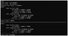
图5为本发明一个实施例提供的一种基于多FPGA的系统静态时序分析方法的setup违例时序报告(部分截图),其中setup slack为建立时间违例时延和、hold slack为保持时间违例时延和、Combinal Port Delay为端口间组合逻辑时延和;5 is a setup violation timing report (partial screenshot) of a multi-FPGA-based system static timing analysis method provided by an embodiment of the present invention, where setup slack is the sum of the setup time violation delays and hold slack is the hold time violation delay and Combinal Port Delay is the combined logical delay sum between ports;
图6为本发明一个实施例提供的一种基于多FPGA的系统静态时序分析方法的hold违例时序报告(部分截图);6 is a hold violation timing report (partial screenshot) of a multi-FPGA-based system static timing analysis method provided by an embodiment of the present invention;
图7为本发明一个实施例提供的一种基于多FPGA的系统静态时序分析方法的端口间组合逻辑时延的时序报告(部分截图);7 is a timing report (partial screenshot) of a combinational logic delay between ports of a multi-FPGA-based system static timing analysis method provided by an embodiment of the present invention;
图8为本发明一个实施例提供的一种基于多FPGA的系统静态时序分析方法的输入文件。FIG. 8 is an input file of a multi-FPGA-based system static timing analysis method provided by an embodiment of the present invention.
具体实施方式Detailed ways
为使本发明的上述目的、特征和优点能够更加明显易懂,下面结合说明书附图对本发明的具体实施方式做详细的说明,显然所描述的实施例是本发明的一部分实施例,而不是全部实施例。基于本发明中的实施例,本领域普通人员在没有做出创造性劳动前提下所获得的所有其他实施例,都应当属于本发明的保护的范围。In order to make the above objects, features and advantages of the present invention more obvious and easy to understand, the specific embodiments of the present invention will be described in detail below with reference to the accompanying drawings. Obviously, the described embodiments are part of the embodiments of the present invention, not all of them. Example. Based on the embodiments of the present invention, all other embodiments obtained by persons of ordinary skill in the art without creative efforts shall fall within the protection scope of the present invention.
在下面的描述中阐述了很多具体细节以便于充分理解本发明,但是本发明还可以采用其他不同于在此描述的其它方式来实施,本领域技术人员可以在不违背本发明内涵的情况下做类似推广,因此本发明不受下面公开的具体实施例的限制。Many specific details are set forth in the following description to facilitate a full understanding of the present invention, but the present invention can also be implemented in other ways different from those described herein, and those skilled in the art can do so without departing from the connotation of the present invention. Similar promotion, therefore, the present invention is not limited by the specific embodiments disclosed below.
其次,此处所称的“一个实施例”或“实施例”是指可包含于本发明至少一个实现方式中的特定特征、结构或特性。在本说明书中不同地方出现的“在一个实施例中”并非均指同一个实施例,也不是单独的或选择性的与其他实施例互相排斥的实施例。Second, reference herein to "one embodiment" or "an embodiment" refers to a particular feature, structure, or characteristic that may be included in at least one implementation of the present invention. The appearances of "in one embodiment" in various places in this specification are not all referring to the same embodiment, nor are they separate or selectively mutually exclusive from other embodiments.
本发明结合示意图进行详细描述,在详述本发明实施例时,为便于说明,表示器件结构的剖面图会不依一般比例作局部放大,而且所述示意图只是示例,其在此不应限制本发明保护的范围。此外,在实际制作中应包含长度、宽度及深度的三维空间尺寸。The present invention is described in detail with reference to the schematic diagrams. When describing the embodiments of the present invention in detail, for the convenience of explanation, the sectional views showing the device structure will not be partially enlarged according to the general scale, and the schematic diagrams are only examples, which should not limit the present invention. scope of protection. In addition, the three-dimensional spatial dimensions of length, width and depth should be included in the actual production.
同时在本发明的描述中,需要说明的是,术语中的“上、下、内和外”等指示的方位或位置关系为基于附图所示的方位或位置关系,仅是为了便于描述本发明和简化描述,而不是指示或暗示所指的装置或元件必须具有特定的方位、以特定的方位构造和操作,因此不能理解为对本发明的限制。此外,术语“第一、第二或第三”仅用于描述目的,而不能理解为指示或暗示相对重要性。At the same time, in the description of the present invention, it should be noted that the orientation or positional relationship indicated in terms such as "upper, lower, inner and outer" is based on the orientation or positional relationship shown in the accompanying drawings, which is only for the convenience of describing the present invention. The invention and simplified description do not indicate or imply that the device or element referred to must have a particular orientation, be constructed and operate in a particular orientation, and therefore should not be construed as limiting the invention. Furthermore, the terms "first, second or third" are used for descriptive purposes only and should not be construed to indicate or imply relative importance.
本发明中除非另有明确的规定和限定,术语“安装、相连、连接”应做广义理解,例如:可以是固定连接、可拆卸连接或一体式连接;同样可以是机械连接、电连接或直接连接,也可以通过中间媒介间接相连,也可以是两个元件内部的连通。对于本领域的普通技术人员而言,可以具体情况理解上述术语在本发明中的具体含义。Unless otherwise expressly specified and limited in the present invention, the term "installation, connection, connection" should be understood in a broad sense, for example: it may be a fixed connection, a detachable connection or an integral connection; it may also be a mechanical connection, an electrical connection or a direct connection. The connection can also be indirectly connected through an intermediate medium, or it can be the internal communication between two elements. For those of ordinary skill in the art, the specific meanings of the above terms in the present invention can be understood in specific situations.
实施例1Example 1
参照图2~8,为本发明的一个实施例,提供了一种,包括:Referring to Figures 2 to 8, an embodiment of the present invention provides a method, including:
S1:根据节点的属性对网表文件进行分类,并生成电路的连接关系图;S1: classify the netlist file according to the attributes of the nodes, and generate the connection diagram of the circuit;
读入网表文件,根据节点的属性对其进行分类,具体分类方法如下:Read in the netlist file and classify the nodes according to their attributes. The specific classification methods are as follows:
1)根据结点名称分成两类结点gx和gpx(其中x=0,1,2…);1) According to the node name, it is divided into two types of nodes gx and gpx (where x=0, 1, 2...);
2)根据design.are文件中结点是否有clk属性以及是否为输入输出端将gpx(其中x=0,1,2…)结点分为输入时钟和gpin或者gpout;2) According to whether the node in the design.are file has the clk attribute and whether it is an input or output terminal, the gpx (where x=0, 1, 2...) nodes are divided into input clock and gpin or gpout;
3)根据design.are文件中结点是否有ff属性将gx(其中x=0,1,2…)分为组合逻辑结点和具有ff属性结点,其中具有ff属性结点根据其无clk属性和是否只作为源点将其分为组合逻辑或者vcc和gnd。具有ff属性的结点且有clk属性的结点是寄存器结点;3) According to whether the node in the design.are file has the ff attribute, gx (where x=0, 1, 2...) is divided into a combinational logic node and a node with the ff attribute, and the node with the ff attribute is based on its no clk Attributes and whether they are only used as source points divide it into combinatorial logic or vcc and gnd. A node with ff attribute and a node with clk attribute is a register node;
4)组合逻辑结点前后所连的结点若均有clk属性且两者的clk值不同,则该组合逻辑结点为分频器。4) If the nodes connected before and after the combinational logic node have the clk attribute and the clk values of the two are different, the combinational logic node is a frequency divider.
节点的分类的依据包括输入文件中提供的节点的属性、命名规则和连接关系,对节点进行分类的目的是确保后续查找路径的准确性。The classification of nodes is based on the attributes, naming rules and connection relationships of the nodes provided in the input file. The purpose of classifying nodes is to ensure the accuracy of the subsequent search paths.
节点的分类的依据包括输入文件中提供的节点的属性、命名规则和连接关系。输入文件包括节点定义文件、节点分组文件、连接定义文件、时钟定义文件、时分复用定义文件,输入网表文件信时对节点定义文件、节点分组文件、连接定义文件、时钟定义文件、时分复用定义文件进行读取,存储在程序中。The classification of nodes is based on the attributes, naming rules and connection relationships of the nodes provided in the input file. Input files include node definition file, node grouping file, connection definition file, clock definition file, time division multiplexing definition file, input netlist file, time-to-node definition file, node grouping file, connection definition file, clock definition file, time division multiplexing file. The definition file is read and stored in the program.
根据节点的属性对其进行分类;通过对节点定义文件(design.are)、节点分组文件(design.node)、连接定义文件(design.net)、时钟定义文件(design.clock)、时分复用定义文件(design.tdm)输入网表信息这五个文件进行读取,存储在程序中;根据时钟的变化标记分频器;通过对四种静态时序分析路径(In->Register、Register->Register、Register->Out、In->Out这四类)分别进行判断和分析,然后通过DFS搜寻路径;最后输出完整的时序报告。Nodes are classified according to their properties; by grouping nodes (design.are), node grouping (design.node), connection definition (design.net), clock The definition file (design.tdm) enters the five files of netlist information to read and store in the program; mark the frequency divider according to the change of the clock; by analyzing the four static timing paths (In->Register, Register-> Register, Register->Out, In->Out (the four categories) are judged and analyzed respectively, and then the path is searched through DFS; finally, a complete timing report is output.
节点的分类是根据design.are文件和design.net文件来判断,具体分为四类:寄存器节点、时钟输入节点、普通输入节点、普通输出节点、组合逻辑单元节点。The classification of nodes is judged according to the design.are file and the design.net file, and is divided into four categories: register nodes, clock input nodes, common input nodes, common output nodes, and combinational logic unit nodes.
通过对节点定义文件(design.are)、节点分组文件(design.node)、连接定义文件(design.net)、时钟定义文件(design.clock)、时分复用定义文件(design.tdm)这五个文件进行读取,并按照上述的分类要求将输入文件存储在程序中。Through the five node definition file (design.are), node grouping file (design.node), connection definition file (design.net), clock definition file (design.clock), time division multiplexing definition file (design.tdm) file is read, and the input file is stored in the program according to the above classification requirements.
互连线分为直连线和TDM传输两种类型,直连线即为直接通过Cable传递单一信号,延时时间固定;TDM传输为多个信号时分复用同一根Cable在FPGA的间传递信号,延时时间可变。The interconnection line is divided into two types: direct connection line and TDM transmission. The direct connection line is to transmit a single signal directly through the Cable, and the delay time is fixed; the TDM transmission is time-division multiplexing of multiple signals. The same Cable transmits signals between FPGAs , the delay time is variable.
S2:从时钟输入端沿着时钟路径开始搜索分频器。S2: Start searching for dividers along the clock path from the clock input.
根据节点名称将节点分为gx和gpx(其中x=0,1,2…);根据节点定义文件中结点是否有clk属性以及是否为输入输出端将gpx(其中x=0,1,2…)结点分为输入时钟和gpin或者gpout;根据节点定义文件中结点是否有ff属性将gx(其中x=0,1,2…)分为组合逻辑结点和具有ff属性结点,其中具有ff属性结点根据其无clk属性和是否只作为源点将其分为组合逻辑或者vcc和gnd,具有ff属性的结点且有clk属性的结点为寄存器结点;组合逻辑结点前后所连的结点若均有clk属性且两者的clk值不同,则该组合逻辑结点为分频器。According to the node name, the nodes are divided into gx and gpx (where x=0, 1, 2...); according to whether the node in the node definition file has the clk attribute and whether it is an input or output, the gpx (where x=0, 1, 2 ...) node is divided into input clock and gpin or gpout; according to whether the node in the node definition file has ff attribute, gx (where x=0, 1, 2...) is divided into combinational logic node and node with ff attribute, The node with ff attribute is divided into combinational logic or vcc and gnd according to whether it has no clk attribute and whether it is only used as a source point. The node with ff attribute and the node with clk attribute is a register node; combinational logic node If the nodes connected before and after have the clk attribute and the clk values of the two are different, the combinational logic node is a frequency divider.
根据时钟的变化标记分频器。在寻找时钟路径时,需要深度搜索来标记分频器,由于分频器只能位于时钟路径上,只需要判断时钟节点连接的组合逻辑的下一个节点是不是寄存器,如果是的话还需满足此寄存器的时钟和分频器前面的时钟不一致。The divider is marked according to the change of the clock. When looking for the clock path, a deep search is required to mark the frequency divider. Since the frequency divider can only be located on the clock path, it is only necessary to determine whether the next node of the combinational logic connected to the clock node is a register. The clock of the register does not match the clock before the divider.
对分频器进行标记后进行搜索时钟路径,标记分频器具体方法为:单独写深度搜索来标记,由于分频器只能位于时钟路径上,只需要判断时钟节点连接的组合逻辑的下一个节点是不是寄存器,如果是的话还需满足此寄存器的时钟和分频器前面的时钟不一致。可以采用深度优先搜索算法(Depth-First-Search,缩写为DFS)或广度优先搜索算法(Breadth-First-Search,缩写为BFS)进行搜索。After marking the frequency divider, search for the clock path. The specific method of marking the frequency divider is: write the depth search to mark it separately. Since the frequency divider can only be located on the clock path, it is only necessary to judge the next combination logic connected to the clock node. Whether the node is a register, and if so, the clock of this register must be inconsistent with the clock in front of the divider. A depth-first search algorithm (Depth-First-Search, abbreviated as DFS) or a breadth-first search algorithm (Breadth-First-Search, abbreviated as BFS) can be used for searching.
时钟路径类型包括:从输入端到触发器、从触发器到触发器、从触发器到输出端和从输入端到输出端,在静态时序分析和计算过程中,把从输入端到触发器和从触发器到输出端路径的输入端和输出端当作虚拟寄存器处理。Clock path types include: from input to flip-flop, from flip-flop to flip-flop, from flip-flop to output, and from input to output. The inputs and outputs of the path from flip-flop to output are treated as virtual registers.
在计算时钟路径时延时:先判断时钟路径的起始节点,起始节点包括数据输入端和寄存器;然后进行DFS遍历搜索路径;每搜到一条路径就对其路径类型进行判断及计算,直到所有的路径都搜索完为止。Delay when calculating the clock path: first determine the starting node of the clock path, which includes the data input terminal and the register; then perform DFS traversal search path; each time a path is found, its path type is judged and calculated, until All paths are searched until exhausted.
在计算数据路径上时延的时候,必须考虑时钟源和寄存器之前存在cable或者TDM的情况,否则会导致延时偏差很大。因此,需要在搜索的时候对时钟路上的延时多一次判断。When calculating the delay on the data path, it is necessary to consider the existence of cables or TDMs before the clock source and registers, otherwise the delay deviation will be large. Therefore, it is necessary to judge the delay on the clock path one more time when searching.
S3:根据起始点类型对整体电路进行遍历搜索路径,对已搜到的路径类型进行判断并计算其时延;S3: traverse the search path for the entire circuit according to the starting point type, judge the searched path type and calculate its time delay;
时钟路径类型包括从输入端到触发器、从触发器到触发器、从触发器到输出端和从输入端到输出端。Clock path types include input to flip-flop, flip-flop to flip-flop, flip-flop to output, and input to output.
计算时钟路径时延时的步骤:先判断时钟路径的起始节点,起始节点包括数据输入端和寄存器;然后进行遍历搜索路径;每搜到一条路径就对其路径类型进行判断及计算。The steps of calculating the time delay of the clock path: first determine the starting node of the clock path, which includes the data input terminal and the register; then traverse the search path; each time a path is found, its path type is judged and calculated.
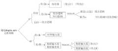
按照STA中的四种时序路径分类为:In->RegisterD、CLK->RegisterD、CLK->Out、In->Out,但是这样在算法实现上就需要不停地往前追溯来区分CK端和D端,实现起来过于复杂。针对这一问题的解决办法是就把D触发器看成一个整体的节点,不对触发器节点进行CK端和D端的分类,把路径分类为In->Register、Register->Register、Register->Out、In->Out这四类,并把第一种和第三种路径的In和Out当作虚拟寄存器处理。在计算每条路径的时延时,首先判断起始节点,这里的起始节点分为两类:数据输入端和寄存器。判断完起始节点后,就开始进行DFS遍历搜索路径,每搜到一条路径就对其路径类型进行判断及计算,如图1所示,直到所有的路径都搜索完为止。According to the four timing paths in STA, they are classified as: In->RegisterD, CLK->RegisterD, CLK->Out, In->Out, but in the implementation of the algorithm, it is necessary to keep going back to distinguish the CK end and the The D side is too complicated to implement. The solution to this problem is to treat the D flip-flop as a whole node, not to classify the CK end and D end of the trigger node, and classify the paths as In->Register, Register->Register, Register->Out , In->Out these four categories, and treat the In and Out of the first and third paths as virtual registers. When calculating the time delay of each path, first determine the starting node, where the starting node is divided into two categories: data input terminal and register. After judging the starting node, the DFS traversal search path is started. Every time a path is found, its path type is judged and calculated, as shown in Figure 1, until all the paths are searched.
通过对四种静态时序分析路径分别进行判断和分析,然后通过DFS搜寻路径。根据四种时序路径,分别写出寄存器到寄存器建立时间检查函数、输入端到寄存器建立时间检查函数、寄存器到输出端建立时间检查函数,使用深度优先算法去遍历时钟节点到寄存器存在的路径以及路径上存在的cable或者TDM延时,分频器也视为时钟节点。求此路径是为了计算In->Register、Register->Register、Register->Out这三种路径的建立时间和保持时间。The four static timing analysis paths are judged and analyzed respectively, and then the paths are searched through DFS. According to the four timing paths, write out the register-to-register setup time check function, the input-to-register setup-time check function, and the register-to-output setup time check function, and use the depth-first algorithm to traverse the path from the clock node to the register and the path The frequency divider is also regarded as a clock node for the existing cable or TDM delay. This path is required to calculate the establishment time and hold time of the three paths In->Register, Register->Register, and Register->Out.
寄存器到寄存器setup slack的计算方法为:The calculation method of register-to-register setup slack is:
data arrival time:Tarrive=Tlaunch+Tco+Tdpdata arrival time: Tarrive=Tlaunch+Tco+Tdp
data expected time:Trequire=Tcapture+Tcycle–Tsudata expected time: Trequire=Tcapture+Tcycle–Tsu
Setup Slack=Trequire–TarriveSetup Slack=Trequire–Tarrive
hold slack的计算方法为:The hold slack is calculated as:
data arrival time:Tarrive=Tlaunch+Tco+Tdpdata arrival time: Tarrive=Tlaunch+Tco+Tdp
data expected time:Trequire=Tcapture+Thddata expected time: Trequire=Tcapture+Thd
hold slack=Tarrive–Trequirehold slack=Tarrive–Trequire
其中,Tcycle为clk的周期(design.clk文件已给出);Among them, Tcycle is the cycle of clk (design.clk file has been given);
Tsu=1nsTsu=1ns
Tco=1nsTco=1ns
Tdp(组合逻辑时延,一个组合逻辑单元的延时为0.1ns)Tdp (combinational logic delay, the delay of a combinational logic unit is 0.1ns)
Thd=1nsThd=1ns
Tlaunch为发射路径延时;Tlaunch is the launch path delay;
Tcapture为捕获路径延时。Tcapture is the capture path delay.
输入端到寄存器setup slack的计算方法为:The calculation method of the input terminal to the register setup slack is:
data arrival time:Tarrive=Tvirtual_launch+Tco+Tdpdata arrival time: Tarrive=Tvirtual_launch+Tco+Tdp
data expected time:Trequire=Tcapture+Tcycle–Tsudata expected time: Trequire=Tcapture+Tcycle–Tsu
Setup Slack=Trequire–TarriveSetup Slack=Trequire–Tarrive
hold slack的计算方法为:The hold slack is calculated as:
data arrival time:Tarrive=Tvirtual_launch+Tco+Tdpdata arrival time: Tarrive=Tvirtual_launch+Tco+Tdp
data expected time:Trequire=Tcapture+Thddata expected time: Trequire=Tcapture+Thd
hold slack=Tarrive–Trequirehold slack=Tarrive–Trequire
其中,Tcycle为clk的周期(design.clk文件已给出);Among them, Tcycle is the cycle of clk (design.clk file has been given);
Tsu=1nsTsu=1ns
Tco=1nsTco=1ns
Tdp(组合逻辑时延,一个组合逻辑单元的延时为0.1ns)Tdp (combinational logic delay, the delay of a combinational logic unit is 0.1ns)
Thd=1nsThd=1ns
Tvirtual_launch为虚拟发射路径延时;Tvirtual_launch is the virtual launch path delay;
Tcapture为捕获路径延时。Tcapture is the capture path delay.
寄存器到输出端setup slack的计算方法为:The calculation method of register to output setup slack is:
data arrival time:Tarrive=Tlaunch+Tco+Tdpdata arrival time: Tarrive=Tlaunch+Tco+Tdp
data expected time:Trequire=Tvirtual_capture+Tcycle–Tsudata expected time: Trequire=Tvirtual_capture+Tcycle–Tsu
Setup Slack=Trequire–TarriveSetup Slack=Trequire–Tarrive
hold slack的计算方法为:The hold slack is calculated as:
data arrival time:Tarrive=Tlaunch+Tco+Tdpdata arrival time: Tarrive=Tlaunch+Tco+Tdp
data expected time:Trequire=Tvirtual_capture+Thddata expected time: Trequire=Tvirtual_capture+Thd
hold slack=Tarrive–Trequirehold slack=Tarrive–Trequire
其中,Tcycle为clk的周期(design.clk文件已给出);Among them, Tcycle is the cycle of clk (design.clk file has been given);
Tsu=1nsTsu=1ns
Tco=1nsTco=1ns
Tdp(组合逻辑时延,一个组合逻辑单元的延时为0.1ns)Tdp (combinational logic delay, the delay of a combinational logic unit is 0.1ns)
Thd=1nsThd=1ns
Tlaunch为发射路径延时;Tlaunch is the launch path delay;
Tvirtual_capture为虚拟捕获路径延时;Tvirtual_capture is the virtual capture path delay;
纯组合逻辑路径的延时计算方法为输入端和输出端所有组合逻辑单元的时延累加和。The delay calculation method for pure combinational logic paths is the cumulative sum of the delays of all combinational logic units at the input and output.
若T1,T2,…,TN为输入端和输出端之间的N个相连的组合逻辑单元,则从输入端到输出端的总延时Ttotal=T1+T2+…+TN。If T1, T2, ..., TN are N connected combinational logic units between the input end and the output end, then the total delay from the input end to the output end Ttotal=T1+T2+...+TN.
对于所给测试例中的特殊情况,以及对于特殊情况的解决方法:For the special cases in the given test cases, and the workarounds for the special cases:
对于所给的测试例里面存在的环路问题。环路是用标记弧或者顶点来确定的,如果标记点的话,不会重复搜索;如果标记弧的话,环路只保存一次,不会无限循环。For the loop problem in the given test case. The loop is determined by marking arcs or vertices. If the points are marked, the search will not be repeated; if the arcs are marked, the loop will only be saved once and will not loop infinitely.
对于所给的测试例里面存在多条路径和多条连线的问题。两点之间多条连线和两点之间多条路径是不一样的,两点之间多条路径会直接搜出来,两点之间的多条连线连线间是等价的,只存了一条线。For the given test case, there are multiple paths and multiple connections. Multiple connections between two points and multiple paths between two points are different. Multiple paths between two points will be found directly. Multiple connections between two points are equivalent. Only one line remains.
优先考虑具有人能够识别的计算优先级,考虑将表达式转换成后缀表达式,将表达式计算优先级展现在表达式的左右顺序上,转换成计算机能够识别的后缀表达式。全部计算流程如下:Priority should be given to the calculation priority that can be recognized by humans, and it is considered to convert expressions into postfix expressions, show the expression calculation priority in the left and right order of expressions, and convert them into postfix expressions that can be recognized by computers. The whole calculation process is as follows:
后缀表达式的计算方法:The calculation method of the postfix expression:
取到后缀表达式的字符串时,从左到右依次遍历。遍历元素处理情况跟如下:When the string of the suffix expression is obtained, it is traversed from left to right. The processing of traversing elements is as follows:
a.遍历元素如果为操作数,则进入维护的栈中,等待取用。a. If the traversal element is an operand, it will enter the maintained stack and wait for it to be accessed.
b.遍历元素如果为操作符,则从维护的栈中弹出两个数,分先后依次为右左操作数,完成相关运算,将计算结果再次入栈。b. If the traversal element is an operator, two numbers are popped from the maintained stack, which are the right and left operands in sequence, and the related operation is completed, and the calculation result is pushed into the stack again.
遍历后缀表达式结束后,所维护的栈中还剩下一个元素,即是所计算的结果。如果栈中元素不是一个,则输出异常信息。After traversing the suffix expression, there is one element left in the maintained stack, which is the calculated result. If the element in the stack is not one, an exception message is output.
转换成后缀表达式的计算过程:The calculation process of converting to a postfix expression:
读取题设文件中缀表达式字符串,依次遍历,遍历元素处理过程如下:Read the infix expression string of the title file, traverse it in turn, and traverse the elements. The processing process is as follows:
维护一个栈,现将栈底标记符(可以取非表达式的任意字符)压入栈底Maintain a stack, and now push the stack bottom marker (which can take any character that is not an expression) into the bottom of the stack
a.遍历元素为操作数时,直接输出。a. When the traversed element is the operand, output directly.
b.遍历元素为输入变量时,(如题设提供为r,进行标记,便于后续的参数输入),同样进行输出。b. When the traversal element is an input variable, (for example, if the title is provided as r, it is marked to facilitate subsequent parameter input), and the output is also performed.
c.遍历元素为右括号”)”,则直接进行连续出栈输出,直到输出到左括号“(”出栈为止,但是左括号不输出。c. The traversal element is the right parenthesis ")", then the continuous pop-up output is performed directly until the output to the left parenthesis "(" is popped off the stack, but the left parenthesis is not output.
d.若遍历元素为操作符或者左括号”(”,则将该元素的栈外优先级与栈顶元素的栈内优先级进行大小比较,若前者小于等于后者,则连续进行出栈输出,直到当前扫描元素的栈外优先级大于栈顶元素的栈内优先级时,停止出栈。此时,再将该扫描元素进栈。d. If the traversed element is an operator or a left parenthesis "(", compare the size of the element's off-stack priority with the on-stack priority of the top element of the stack, and if the former is less than or equal to the latter, the stack output is continuously performed. , until the out-of-stack priority of the currently scanned element is greater than the in-stack priority of the top element of the stack, stop popping. At this point, push the scanned element into the stack.
e.遍历结束时,依次输出栈中其他元素(栈底标记符除外)。e. At the end of the traversal, output other elements in the stack in turn (except for the stack bottom marker).
完成后缀表达式的转换后,即可保存。After the conversion of the postfix expression is completed, it can be saved.
留至步骤a,进行后缀表达式的计算。Leave it to step a to calculate the postfix expression.
表1、栈内与栈外优先级表。Table 1. In-stack and out-of-stack priority table.

S4:建立时间违例路径、保持时间违例路径以及端口间组合逻辑路径的时序报告。S4: Timing reports for setup time violation paths, hold time violation paths, and combinatorial logic paths between ports.
时序报告包括建立时间违例时延累加和、保持时间违例时延累加和、top20的建立时间违例路径、top20的保持时间违例路径、top20端口间组合逻辑关键路径。在时序报告中按照顺序建立出了setup违例时延累加和、hold违例时延累加和、top20的建立时间违例路径、top20的保持时间违例路径、top20端口间组合逻辑关键路径,如果没有违例路径的情况下,则不建立违例路径。能够检查每条路径的建立时间和保持时间,不仅检查单FPGA电路内部的时序路径,还有多FPGA之间通过插入cable或者TDM方式引入延时信息后的时序路径是否满足建立时间和保持时间要求。在时序报告中按照违例延时的顺序,建立出了setup违例时延累加和、hold违例时延累加和、top20的建立时间违例路径、top20的保持时间违例路径、top20端口间组合逻辑关键路径,能够对FPGA内部时序路径建立时间和保持时间是否满足时序要求进行分析,能够对分割后两块FPGA之间通过互连线的方式引入延时信息后的时序路径是否满足建立时间和保持时间要求进行分析,能够满足对超大规模集成电路的多FPGA芯片进行静态时序分析的要求。The timing report includes the cumulative sum of setup time violation delays, the cumulative sum of hold time violation delays, the top 20 setup time violation paths, the top 20 hold time violation paths, and the top 20 combinatorial logic critical paths between ports. In the timing report, the cumulative sum of setup violation delays, the cumulative sum of hold violation delays, the top20 setup time violation path, the top20 hold time violation path, and the top20 combinatorial logic critical path between ports are established in sequence. If there is no violation path In this case, the violating path is not established. It can check the setup time and hold time of each path, not only the timing paths within a single FPGA circuit, but also whether the timing paths between multiple FPGAs after delay information is introduced by inserting cables or TDM methods meet the setup time and hold time requirements. . In the timing report, according to the order of violation delays, the cumulative sum of setup violation delays, the cumulative sum of hold violation delays, the top20 setup time violation path, the top20 hold time violation path, and the top20 combinatorial logic critical path between ports are established. It can analyze whether the establishment time and hold time of the internal timing path of the FPGA meet the timing requirements, and whether the timing path after the delay information is introduced between the two FPGAs after being divided by the interconnection line meets the requirements of the establishment time and hold time. The analysis can meet the requirements of static timing analysis for multi-FPGA chips of VLSI.
实施例2Example 2
参照图2~8,为本发明另一个实施例,该实施例不同于第一个实施例的是,提供了一种基于多FPGA的系统静态时序分析方法的验证测试,为对本方法中采用的技术效果加以验证说明,本实施例采用传统技术方案与本发明方法进行对比测试,以科学论证的手段对比试验结果,以验证本方法所具有的真实效果。2 to 8 are another embodiment of the present invention, which is different from the first embodiment in that it provides a verification test of a system static timing analysis method based on multiple FPGAs. The technical effect is verified and explained, this embodiment adopts the traditional technical solution and the method of the present invention to carry out a comparative test, and compares the test results by means of scientific demonstration to verify the real effect of the method.
优选的,本实施例为了更便于非本技术领域人员对本发明的理解,分别从以下四个方面进行单独解释说明,五个输入文件说明如下:Preferably, in order to facilitate the understanding of the present invention by those not skilled in the art, this embodiment is separately explained and explained from the following four aspects, and the five input files are explained as follows:
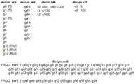
本实施例中的五个输入文件:design.are、design.net、design.node、design.clk、design.tdm皆由软件生成,下面依次对这五个文件进行说明:The five input files in this embodiment: design.are, design.net, design.node, design.clk, and design.tdm are all generated by the software, and the five files are described in sequence below:
design.are:每个节点名称以字母g和一个不重复的数字组成,每行表示一个节点名称和时延属性及相关信息。design.are: Each node name consists of the letter g and a unique number, and each line represents a node name and delay attributes and related information.
design.net:每个连线信息由2个或更多节点组成,一个为驱动节点(s),其他为负载节点(l),每行表示一个连线的部分信息。design.net: Each connection information consists of 2 or more nodes, one is the driving node (s), the other is the load node (l), and each line represents part of the information of a connection.
design.node:分割结果文件,由分割算法根据当前的分割策略和模式运算得出的最优结果。每一行包含一个分组信息里面包含的节点列表。design.node: The segmentation result file, the optimal result obtained by the segmentation algorithm according to the current segmentation strategy and mode operation. Each line contains a list of nodes contained within the grouping information.
design.clk:每行表示一个clock的名称、频率及相关信息。design.clk: Each line represents the name, frequency and related information of a clock.
design.tdm:每行表示一个TDM的名称、时延计算公式。design.tdm: Each line represents the name and delay calculation formula of a TDM.
其中setup slack和hold slack计算公式Where setup slack and hold slack calculation formula
setup slack的计算方法为:The calculation method of setup slack is:
data arrival time:Tarrive=Tco+TdpData arrival time: Tarrive=Tco+Tdp
data expected time:Trequire=Tcycle–Tsudata expected time: Trequire=Tcycle–Tsu
Setup Slack=Trequire–TarriveSetup Slack=Trequire–Tarrive
hold slack的计算方法为:The hold slack is calculated as:
data arrival time:Tarrive=Tco+TdpData arrival time: Tarrive=Tco+Tdp
data expected time;Trequire=Thddata expected time; Trequire=Thd
hold slack=Tarrive–Trequirehold slack=Tarrive–Trequire
其中,Tcycle为clk的周期(design.clk文件已给出);Among them, Tcycle is the cycle of clk (design.clk file has been given);
Tsu=1nsTsu=1ns
Tco=1nsTco=1ns
Tdp(组合逻辑时延,一个组合逻辑单元的延时为0.1ns)Tdp (combinational logic delay, the delay of a combinational logic unit is 0.1ns)
Thd=1nsThd=1ns
表2、测试项及其描述表。Table 2. Test items and their descriptions.
表3、测试结果统计表。Table 3. Statistics of test results.
由于搜索算法采用的是DFS算法,而DFS算法是一个递归算法,需要借助一个递归工作栈,故它的空间复杂度为O(V)。遍历图的过程实质上是对每个顶点查找其邻接点的过程,其耗费的时间取决于所采用结构。本程序中采用邻接表存储图,查找所有顶点的邻接点所需时间为O(E),访问顶点的邻接点所花时间为O(V),此时,总的时间复杂度为O(V+E)。其中,V是结点个数,E是结点之间连线个数。Since the search algorithm uses the DFS algorithm, and the DFS algorithm is a recursive algorithm, it needs to use a recursive work stack, so its space complexity is O(V). The process of traversing the graph is essentially the process of finding its neighbors for each vertex, and the time it takes depends on the structure used. In this program, the adjacency list is used to store the graph. The time required to find the adjacent points of all vertices is O(E), and the time spent to access the adjacent points of the vertices is O(V). At this time, the total time complexity is O(V +E). Among them, V is the number of nodes, and E is the number of connections between nodes.
应当认识到,本发明的实施例可以由计算机硬件、硬件和软件的组合、或者通过存储在非暂时性计算机可读存储器中的计算机指令来实现或实施。方法可以使用标准编程技术包括配置有计算机程序的非暂时性计算机可读存储介质在计算机程序中实现,其中如此配置的存储介质使得计算机以特定和预定义的方式操作——根据在具体实施例中描述的方法和附图。每个程序可以以高级过程或面向对象的编程语言来实现以与计算机系统通信。然而,若需要,该程序可以以汇编或机器语言实现。在任何情况下,该语言可以是编译或解释的语言。此外,为此目的该程序能够在可编程的专用集成电路上运行。It should be appreciated that embodiments of the present invention may be implemented or implemented by computer hardware, a combination of hardware and software, or by computer instructions stored in non-transitory computer readable memory. The methods may be implemented in a computer program using standard programming techniques, including a non-transitory computer-readable storage medium configured with a computer program, wherein the storage medium so configured causes a computer to operate in a specific and predefined manner - according to specific embodiments described methods and drawings. Each program may be implemented in a high-level procedural or object-oriented programming language to communicate with a computer system. However, if desired, the program can be implemented in assembly or machine language. In any case, the language can be a compiled or interpreted language. Furthermore, the program can be run on a programmable application specific integrated circuit for this purpose.
此外,可按任何合适的顺序来执行本文描述的过程的操作,除非本文另外指示或以其他方式明显地与上下文矛盾。本文描述的过程(或变型和/或其组合)可在配置有可执行指令的一个或多个计算机系统的控制下执行,并且可作为共同地在一个或多个处理器上执行的代码(例如,可执行指令、一个或多个计算机程序或一个或多个应用)、由硬件或其组合来实现。所述计算机程序包括可由一个或多个处理器执行的多个指令。Furthermore, the operations of the processes described herein may be performed in any suitable order unless otherwise indicated herein or otherwise clearly contradicted by context. The processes (or variations and/or combinations thereof) described herein can be performed under the control of one or more computer systems configured with executable instructions, and as code that executes collectively on one or more processors (eg, , executable instructions, one or more computer programs or one or more applications), implemented in hardware, or a combination thereof. The computer program includes a plurality of instructions executable by one or more processors.
进一步,所述方法可以在可操作地连接至合适的任何类型的计算平台中实现,包括但不限于个人电脑、迷你计算机、主框架、工作站、网络或分布式计算环境、单独的或集成的计算机平台、或者与带电粒子工具或其它成像装置通信等等。本发明的各方面可以以存储在非暂时性存储介质或设备上的机器可读代码来实现,无论是可移动的还是集成至计算平台,如硬盘、光学读取和/或写入存储介质、RAM、ROM等,使得其可由可编程计算机读取,当存储介质或设备由计算机读取时可用于配置和操作计算机以执行在此所描述的过程。此外,机器可读代码,或其部分可以通过有线或无线网络传输。当此类媒体包括结合微处理器或其他数据处理器实现上文所述步骤的指令或程序时,本文所述的发明包括这些和其他不同类型的非暂时性计算机可读存储介质。当根据本发明所述的方法和技术编程时,本发明还包括计算机本身。计算机程序能够应用于输入数据以执行本文所述的功能,从而转换输入数据以生成存储至非易失性存储器的输出数据。输出信息还可以应用于一个或多个输出设备如显示器。在本发明优选的实施例中,转换的数据表示物理和有形的对象,包括显示器上产生的物理和有形对象的特定视觉描绘。Further, the methods may be implemented in any type of computing platform operably connected to a suitable, including but not limited to personal computer, minicomputer, mainframe, workstation, network or distributed computing environment, stand-alone or integrated computer platform, or communicate with charged particle tools or other imaging devices, etc. Aspects of the invention may be implemented in machine-readable code stored on a non-transitory storage medium or device, whether removable or integrated into a computing platform, such as a hard disk, an optically read and/or written storage medium, RAM, ROM, etc., such that it can be read by a programmable computer, when a storage medium or device is read by a computer, it can be used to configure and operate the computer to perform the processes described herein. Furthermore, the machine-readable code, or portions thereof, may be transmitted over wired or wireless networks. The invention described herein includes these and other various types of non-transitory computer-readable storage media when such media includes instructions or programs that implement the steps described above in conjunction with a microprocessor or other data processor. The invention also includes the computer itself when programmed according to the methods and techniques described herein. A computer program can be applied to input data to perform the functions described herein, transforming the input data to generate output data for storage to non-volatile memory. The output information can also be applied to one or more output devices such as a display. In a preferred embodiment of the invention, the transformed data represents physical and tangible objects, including specific visual depictions of physical and tangible objects produced on the display.
如在本申请所使用的,术语“组件”、“模块”、“系统”等等旨在指代计算机相关实体,该计算机相关实体可以是硬件、固件、硬件和软件的结合、软件或者运行中的软件。例如,组件可以是,但不限于是:在处理器上运行的处理、处理器、对象、可执行文件、执行中的线程、程序和/或计算机。作为示例,在计算设备上运行的应用和该计算设备都可以是组件。一个或多个组件可以存在于执行中的过程和/或线程中,并且组件可以位于一个计算机中以及/或者分布在两个或更多个计算机之间。此外,这些组件能够从在其上具有各种数据结构的各种计算机可读介质中执行。这些组件可以通过诸如根据具有一个或多个数据分组(例如,来自一个组件的数据,该组件与本地系统、分布式系统中的另一个组件进行交互和/或以信号的方式通过诸如互联网之类的网络与其它系统进行交互)的信号,以本地和/或远程过程的方式进行通信。As used in this application, the terms "component," "module," "system," etc. are intended to refer to a computer-related entity, which may be hardware, firmware, a combination of hardware and software, software, or running software. For example, a component can be, but is not limited to, a process running on a processor, a processor, an object, an executable, a thread in execution, a program, and/or a computer. As an example, both an application running on a computing device and the computing device may be components. One or more components can exist in a process and/or thread of execution, and a component can be localized on one computer and/or distributed between two or more computers. In addition, these components can execute from various computer readable media having various data structures thereon. These components can be implemented by, for example, having one or more data groupings (eg, data from one component interacting with another component in a local system, a distributed system, and/or in a signaling manner such as the Internet network to interact with other systems) to communicate locally and/or as remote processes.
应说明的是,以上实施例仅用以说明本发明的技术方案而非限制,尽管参照较佳实施例对本发明进行了详细说明,本领域的普通技术人员应当理解,可以对本发明的技术方案进行修改或者等同替换,而不脱离本发明技术方案的精神和范围,其均应涵盖在本发明的权利要求范围当中。It should be noted that the above embodiments are only used to illustrate the technical solutions of the present invention and not to limit them. Although the present invention has been described in detail with reference to the preferred embodiments, those of ordinary skill in the art should understand that the technical solutions of the present invention can be Modifications or equivalent substitutions without departing from the spirit and scope of the technical solutions of the present invention should be included in the scope of the claims of the present invention.
Claims (8)
Priority Applications (1)
| Application Number | Priority Date | Filing Date | Title |
|---|---|---|---|
| CN202210257478.7ACN114742001B (en) | 2022-03-16 | 2022-03-16 | System static time sequence analysis method based on multiple FPGA |
Applications Claiming Priority (1)
| Application Number | Priority Date | Filing Date | Title |
|---|---|---|---|
| CN202210257478.7ACN114742001B (en) | 2022-03-16 | 2022-03-16 | System static time sequence analysis method based on multiple FPGA |
Publications (2)
| Publication Number | Publication Date |
|---|---|
| CN114742001Atrue CN114742001A (en) | 2022-07-12 |
| CN114742001B CN114742001B (en) | 2023-08-29 |
Family
ID=82276813
Family Applications (1)
| Application Number | Title | Priority Date | Filing Date |
|---|---|---|---|
| CN202210257478.7AActiveCN114742001B (en) | 2022-03-16 | 2022-03-16 | System static time sequence analysis method based on multiple FPGA |
Country Status (1)
| Country | Link |
|---|---|
| CN (1) | CN114742001B (en) |
Cited By (10)
| Publication number | Priority date | Publication date | Assignee | Title |
|---|---|---|---|---|
| CN115544929A (en)* | 2022-11-30 | 2022-12-30 | 中科亿海微电子科技(苏州)有限公司 | Method and device for testing path time sequence delay in FPGA EDA software |
| CN115600535A (en)* | 2022-12-09 | 2023-01-13 | 中科亿海微电子科技(苏州)有限公司(Cn) | Method and device for performing time sequence analysis on FPGA dynamic reconfigurable area |
| CN115758966A (en)* | 2022-11-15 | 2023-03-07 | 哈尔滨工业大学(深圳) | Propagation method, processing method and medium of timing exception constraints and timing constraints |
| CN115964975A (en)* | 2022-12-30 | 2023-04-14 | 芯耀辉科技有限公司 | Static timing analysis method and system thereof, and computer-readable medium |
| CN116090383A (en)* | 2022-12-27 | 2023-05-09 | 广东高云半导体科技股份有限公司 | Method, device, computer storage medium and terminal for realizing static time sequence analysis |
| CN116108783A (en)* | 2023-04-04 | 2023-05-12 | 上海思尔芯技术股份有限公司 | Method, system, equipment and medium for modeling and processing block logic time sequence analysis |
| CN116502578A (en)* | 2023-06-29 | 2023-07-28 | 深圳国微晶锐技术有限公司 | Construction method of netlist reduction time sequence model and static time sequence analysis method |
| CN117787163A (en)* | 2023-12-28 | 2024-03-29 | 苏州异格技术有限公司 | A timing analysis method, device, equipment and medium based on graph traversal |
| CN117787162A (en)* | 2023-12-27 | 2024-03-29 | 苏州异格技术有限公司 | A multi-terminal angle static timing analysis method, device, computer equipment and medium |
| CN119312748A (en)* | 2024-12-16 | 2025-01-14 | 中科亿海微电子科技(苏州)有限公司 | A time series report analysis method |
Citations (14)
| Publication number | Priority date | Publication date | Assignee | Title |
|---|---|---|---|---|
| US8261218B1 (en)* | 2008-08-01 | 2012-09-04 | Altera Corporation | Systems and methods for determining beneficial clock-path connection delays |
| US20160161551A1 (en)* | 2013-07-26 | 2016-06-09 | Mentor Graphics Corporation | Automated method for analyzing a board having a plurality of fpga components |
| CN105808795A (en)* | 2014-12-29 | 2016-07-27 | 京微雅格(北京)科技有限公司 | FPGA chip global placement optimization method based on temporal constraint |
| CN106096171A (en)* | 2016-06-22 | 2016-11-09 | 深圳市紫光同创电子有限公司 | Asynchronous circuit sequential inspection method based on static analysis |
| CN107862154A (en)* | 2017-11-29 | 2018-03-30 | 成都锐成芯微科技股份有限公司 | A kind of timing adjusting method |
| WO2018076735A1 (en)* | 2016-10-31 | 2018-05-03 | 深圳市中兴微电子技术有限公司 | Method and device for repairing hold time violation, and computer storage medium |
| CN108073771A (en)* | 2017-12-25 | 2018-05-25 | 中国电子科技集团公司第四十七研究所 | FPGA static timing analysis algorithms |
| CN108173617A (en)* | 2017-11-21 | 2018-06-15 | 北京兰云科技有限公司 | A kind of the whole network clock topology and clock method for obtaining path |
| CN109583103A (en)* | 2018-12-04 | 2019-04-05 | 珠海市微半导体有限公司 | A kind of time sequence repairing method based on time margin |
| US20200026818A1 (en)* | 2018-07-23 | 2020-01-23 | Sandisk Technologies Llc | Less-pessimistic static timing analysis for synchronous circuits |
| CN111950214A (en)* | 2020-08-14 | 2020-11-17 | Oppo广东移动通信有限公司 | A timing analysis method, apparatus, device and computer storage medium |
| CN112666451A (en)* | 2021-03-15 | 2021-04-16 | 南京邮电大学 | Integrated circuit scanning test vector generation method |
| CN113177380A (en)* | 2021-04-29 | 2021-07-27 | 飞腾信息技术有限公司 | Time sequence optimization method based on dummy |
| CN113971383A (en)* | 2020-07-24 | 2022-01-25 | 美商新思科技有限公司 | Distributed static timing analysis |
- 2022
- 2022-03-16CNCN202210257478.7Apatent/CN114742001B/enactiveActive
Patent Citations (14)
| Publication number | Priority date | Publication date | Assignee | Title |
|---|---|---|---|---|
| US8261218B1 (en)* | 2008-08-01 | 2012-09-04 | Altera Corporation | Systems and methods for determining beneficial clock-path connection delays |
| US20160161551A1 (en)* | 2013-07-26 | 2016-06-09 | Mentor Graphics Corporation | Automated method for analyzing a board having a plurality of fpga components |
| CN105808795A (en)* | 2014-12-29 | 2016-07-27 | 京微雅格(北京)科技有限公司 | FPGA chip global placement optimization method based on temporal constraint |
| CN106096171A (en)* | 2016-06-22 | 2016-11-09 | 深圳市紫光同创电子有限公司 | Asynchronous circuit sequential inspection method based on static analysis |
| WO2018076735A1 (en)* | 2016-10-31 | 2018-05-03 | 深圳市中兴微电子技术有限公司 | Method and device for repairing hold time violation, and computer storage medium |
| CN108173617A (en)* | 2017-11-21 | 2018-06-15 | 北京兰云科技有限公司 | A kind of the whole network clock topology and clock method for obtaining path |
| CN107862154A (en)* | 2017-11-29 | 2018-03-30 | 成都锐成芯微科技股份有限公司 | A kind of timing adjusting method |
| CN108073771A (en)* | 2017-12-25 | 2018-05-25 | 中国电子科技集团公司第四十七研究所 | FPGA static timing analysis algorithms |
| US20200026818A1 (en)* | 2018-07-23 | 2020-01-23 | Sandisk Technologies Llc | Less-pessimistic static timing analysis for synchronous circuits |
| CN109583103A (en)* | 2018-12-04 | 2019-04-05 | 珠海市微半导体有限公司 | A kind of time sequence repairing method based on time margin |
| CN113971383A (en)* | 2020-07-24 | 2022-01-25 | 美商新思科技有限公司 | Distributed static timing analysis |
| CN111950214A (en)* | 2020-08-14 | 2020-11-17 | Oppo广东移动通信有限公司 | A timing analysis method, apparatus, device and computer storage medium |
| CN112666451A (en)* | 2021-03-15 | 2021-04-16 | 南京邮电大学 | Integrated circuit scanning test vector generation method |
| CN113177380A (en)* | 2021-04-29 | 2021-07-27 | 飞腾信息技术有限公司 | Time sequence optimization method based on dummy |
Non-Patent Citations (5)
| Title |
|---|
| 周海斌: "静态时序分析在高速FPGA设计中的应用", 《电子工程师》* |
| 周海斌: "静态时序分析在高速FPGA设计中的应用", 《电子工程师》, no. 11, 15 November 2005 (2005-11-15), pages 41 - 44* |
| 喻伟;陈恩耀;马海燕;祝周荣;宋雷军;王永孟;: "一种基于时延配置表的FPGA静态时序分析算法", 太赫兹科学与电子信息学报, no. 04, pages 735 - 741* |
| 王冬: "FPGA静态时序约束方法分析", 《空间电子技术》* |
| 王冬: "FPGA静态时序约束方法分析", 《空间电子技术》, no. 05, 25 October 2017 (2017-10-25), pages 103 - 106* |
Cited By (13)
| Publication number | Priority date | Publication date | Assignee | Title |
|---|---|---|---|---|
| CN115758966A (en)* | 2022-11-15 | 2023-03-07 | 哈尔滨工业大学(深圳) | Propagation method, processing method and medium of timing exception constraints and timing constraints |
| CN115544929A (en)* | 2022-11-30 | 2022-12-30 | 中科亿海微电子科技(苏州)有限公司 | Method and device for testing path time sequence delay in FPGA EDA software |
| CN115600535A (en)* | 2022-12-09 | 2023-01-13 | 中科亿海微电子科技(苏州)有限公司(Cn) | Method and device for performing time sequence analysis on FPGA dynamic reconfigurable area |
| CN116090383A (en)* | 2022-12-27 | 2023-05-09 | 广东高云半导体科技股份有限公司 | Method, device, computer storage medium and terminal for realizing static time sequence analysis |
| CN115964975B (en)* | 2022-12-30 | 2023-09-05 | 芯耀辉科技有限公司 | Static timing analysis method and system thereof, and computer-readable medium |
| CN115964975A (en)* | 2022-12-30 | 2023-04-14 | 芯耀辉科技有限公司 | Static timing analysis method and system thereof, and computer-readable medium |
| CN116108783A (en)* | 2023-04-04 | 2023-05-12 | 上海思尔芯技术股份有限公司 | Method, system, equipment and medium for modeling and processing block logic time sequence analysis |
| CN116502578A (en)* | 2023-06-29 | 2023-07-28 | 深圳国微晶锐技术有限公司 | Construction method of netlist reduction time sequence model and static time sequence analysis method |
| CN116502578B (en)* | 2023-06-29 | 2024-04-16 | 深圳国微晶锐技术有限公司 | Construction method of timing model for netlist simplification and static timing analysis method |
| CN117787162A (en)* | 2023-12-27 | 2024-03-29 | 苏州异格技术有限公司 | A multi-terminal angle static timing analysis method, device, computer equipment and medium |
| CN117787163A (en)* | 2023-12-28 | 2024-03-29 | 苏州异格技术有限公司 | A timing analysis method, device, equipment and medium based on graph traversal |
| CN117787163B (en)* | 2023-12-28 | 2024-12-06 | 苏州异格技术有限公司 | A time series analysis method, device, equipment and medium based on graph traversal |
| CN119312748A (en)* | 2024-12-16 | 2025-01-14 | 中科亿海微电子科技(苏州)有限公司 | A time series report analysis method |
Also Published As
| Publication number | Publication date |
|---|---|
| CN114742001B (en) | 2023-08-29 |
Similar Documents
| Publication | Publication Date | Title |
|---|---|---|
| CN114742001B (en) | System static time sequence analysis method based on multiple FPGA | |
| US10990725B2 (en) | Clock-gating phase algebra for clock analysis | |
| US7162706B2 (en) | Method for analyzing and validating clock integration properties in circuit systems | |
| US20050091025A1 (en) | Methods and systems for improved integrated circuit functional simulation | |
| US8136077B2 (en) | Timing-optimal placement, pin assignment, and routing for integrated circuits | |
| US9244810B2 (en) | Debugger graphical user interface system, method, and computer program product | |
| US7917884B2 (en) | Enhanced verification by closely coupling a structural overapproximation algorithm and a structural satisfiability solver | |
| JP2001142937A (en) | Scheduling correctness checking method and schedule verifying method for circuit | |
| US8943448B2 (en) | System, method, and computer program product for providing a debugger using a common hardware database | |
| US8701059B2 (en) | Method and system for repartitioning a hierarchical circuit design | |
| US9171115B2 (en) | System, method, and computer program product for translating a common hardware database into a logic code model | |
| US20080092091A1 (en) | Method and system for reduction of XOR/XNOR subexpressions in structural design representations | |
| US20180107776A1 (en) | Phase algebra for analysis of hierarchical designs | |
| US20110078644A1 (en) | Asychronous system analysis | |
| US7882459B2 (en) | Method and system for reduction of AND/OR subexpressions in structural design representations | |
| Vahid et al. | Functional partitioning improvements over structural partitioning for packaging constraints and synthesis: tool performance | |
| US8959467B2 (en) | Structural rule analysis with TCL scripts in synthesis or STA tools and integrated circuit design tools | |
| Huang et al. | A robust ECO engine by resource-constraint-aware technology mapping and incremental routing optimization | |
| US8904318B1 (en) | Method and apparatus for performing optimization using don't care states | |
| Tie et al. | A Method of Extracting and Visualizing Hierarchical Structure of Hardware Logic Based on Tree-Structure For FPGA-Based Prototyping | |
| Nie et al. | Machine Learning Method for Predicting Circuit Timing Using Complex Network | |
| Barbhaya et al. | An Open-Source Static Timing Analysis EDA Tool for Digital System Design | |
| Tong et al. | Performance-driven register insertion in placement | |
| Xu et al. | Efficient Hypergraph Modeling of VLSI Circuits for the MFS-Based Emulation and Simulation Acceleration | |
| Najafiuchevler et al. | Modelling and Assertion-Based Verification of Run-Time Reconfigurable Designs Using Functional Programming Abstractions |
Legal Events
| Date | Code | Title | Description |
|---|---|---|---|
| PB01 | Publication | ||
| PB01 | Publication | ||
| SE01 | Entry into force of request for substantive examination | ||
| SE01 | Entry into force of request for substantive examination | ||
| GR01 | Patent grant | ||
| GR01 | Patent grant |