CN114741350A - A method, system, device and medium for cascading multiple NVME hard disk backplanes - Google Patents
A method, system, device and medium for cascading multiple NVME hard disk backplanesDownload PDFInfo
- Publication number
- CN114741350A CN114741350ACN202210474160.4ACN202210474160ACN114741350ACN 114741350 ACN114741350 ACN 114741350ACN 202210474160 ACN202210474160 ACN 202210474160ACN 114741350 ACN114741350 ACN 114741350A
- Authority
- CN
- China
- Prior art keywords
- backplane
- hard disk
- address
- nvme hard
- signal
- Prior art date
- Legal status (The legal status is an assumption and is not a legal conclusion. Google has not performed a legal analysis and makes no representation as to the accuracy of the status listed.)
- Withdrawn
Links
Images


Classifications
- G—PHYSICS
- G06—COMPUTING OR CALCULATING; COUNTING
- G06F—ELECTRIC DIGITAL DATA PROCESSING
- G06F13/00—Interconnection of, or transfer of information or other signals between, memories, input/output devices or central processing units
- G06F13/38—Information transfer, e.g. on bus
- G06F13/42—Bus transfer protocol, e.g. handshake; Synchronisation
- G06F13/4247—Bus transfer protocol, e.g. handshake; Synchronisation on a daisy chain bus
- G—PHYSICS
- G06—COMPUTING OR CALCULATING; COUNTING
- G06F—ELECTRIC DIGITAL DATA PROCESSING
- G06F11/00—Error detection; Error correction; Monitoring
- G06F11/30—Monitoring
- G06F11/32—Monitoring with visual or acoustical indication of the functioning of the machine
- G06F11/324—Display of status information
- G06F11/325—Display of status information by lamps or LED's
- G—PHYSICS
- G06—COMPUTING OR CALCULATING; COUNTING
- G06F—ELECTRIC DIGITAL DATA PROCESSING
- G06F2213/00—Indexing scheme relating to interconnection of, or transfer of information or other signals between, memories, input/output devices or central processing units
- G06F2213/0026—PCI express
Landscapes
- Engineering & Computer Science (AREA)
- Theoretical Computer Science (AREA)
- Physics & Mathematics (AREA)
- General Engineering & Computer Science (AREA)
- General Physics & Mathematics (AREA)
- Quality & Reliability (AREA)
- Debugging And Monitoring (AREA)
Abstract
Translated fromChinese
Description
Translated fromChinese技术领域technical field
本发明涉及NVME硬盘背板级联技术领域,尤其是指一种多个NVME硬盘背板级联方法、系统、设备及介质。The invention relates to the technical field of NVME hard disk backplane cascading, in particular to a method, system, device and medium for cascading multiple NVME hard disk backplanes.
背景技术Background technique
随着人工智能及大数据等业务需求的快速发展,大容量存储、人工智能等服务器的需求日益增加。With the rapid development of business needs such as artificial intelligence and big data, the demand for servers such as large-capacity storage and artificial intelligence is increasing.
为满足人们对于服务器性能及多种配置兼容的使用要求,主板的CPU(CentralProcessing Unit,即中央处理器)作为NVME(Non-Volatile Memory express,即非易失性内存主机控制器接口规范)硬盘PCIE信号的HOST端,每个CPU都有多个X16的PCIE Port口,根据配置的不同,可以配置为X4、X8、X16;NVME硬盘(PCIE X4)具有现有读写速率高的特性,在数据高速存储及读取要求市场上需求较大。In order to meet people's requirements for server performance and compatibility with various configurations, the motherboard's CPU (Central Processing Unit, central processing unit) is used as NVME (Non-Volatile Memory express, non-volatile memory host controller interface specification) hard disk PCIE On the HOST side of the signal, each CPU has multiple X16 PCIE ports, which can be configured as X4, X8, and X16 depending on the configuration; High-speed storage and reading requirements are in great demand in the market.
通常主板通过MCIO/Slimline连接器传输CPU PCIE高速信号及Sideband信号,不同CPU的PCIE Port口下挂的Device需要不同。为了满足服务器主板CPU的每个X16可以配置成为X4、单个背板支持CPU Balance及服务器NVME硬盘序排列及点灯等要求,通常两路的主板需要在每个MCIO/Slimline连接器的Sideband信号中设定6位VPP地址信号;同时需要单独于背板Sideband连接器上VPP(Virtual Point Protocol,即虚拟接口协议)和BMC(Baseboard Management Controller,即基板管理控制器)处的I2C信号。Usually, the motherboard transmits CPU PCIE high-speed signals and Sideband signals through the MCIO/Slimline connector, and the devices connected to the PCIE Port of different CPUs need to be different. In order to meet the requirements that each X16 of the server motherboard CPU can be configured as X4, a single backplane supports CPU Balance, and the server NVME hard disk sequence and lighting requirements, usually two-way motherboards need to be set in the Sideband signal of each MCIO/Slimline connector. Locate the 6-bit VPP address signal; at the same time, it needs to be separated from the I2C signal at the VPP (Virtual Point Protocol, ie virtual interface protocol) and BMC (Baseboard Management Controller, ie baseboard management controller) on the sideband connector of the backplane.
随着现有服务器主板CPU的PCIE资源数量增长、以及主板上的CPU数量增加,主板在每个MCIO/Slimline连接器VPP地址信号数量还需要增加;同时,为支持多种PCIE设备的识别和控制、从而使连接器上的其他Sideband信号数量增加,易出现MCIO/Slimline连接器上的Sideband管脚数量不够使用的情况。With the increase in the number of PCIE resources of the existing server motherboard CPU and the increase in the number of CPUs on the motherboard, the number of VPP address signals in each MCIO/Slimline connector of the motherboard needs to be increased; at the same time, in order to support the identification and control of various PCIE devices , so as to increase the number of other Sideband signals on the connector, and it is prone to the situation that the number of Sideband pins on the MCIO/Slimline connector is not enough for use.
为此,需要改进现有技术,来解决服务器中上述技术问题。Therefore, it is necessary to improve the existing technology to solve the above-mentioned technical problems in the server.
发明内容SUMMARY OF THE INVENTION
为了解决上述技术问题,本发明提供了一种多个NVME硬盘背板级联方法、系统、设备及介质,所述多个NVME硬盘背板级联方法用于解决目前服务器中NVME硬盘背板连接器管脚、CPLD管脚等管脚资源不够使用的问题。In order to solve the above technical problems, the present invention provides a method, system, device and medium for cascading multiple NVME hard disk backplanes. Insufficient use of pin resources such as device pins and CPLD pins.
为实现上述目的,本发明提供一种多个NVME硬盘背板级联方法,包括:In order to achieve the above object, the present invention provides a method for cascading multiple NVME hard disk backplanes, including:
将主板与多个NVME硬盘背板依次按菊花链形式进行级联,对每个NVME硬盘背板设置唯一的背板地址;The mainboard and multiple NVME hard disk backplanes are cascaded in sequence in a daisy-chain form, and a unique backplane address is set for each NVME hard disk backplane;
将NVME硬盘背板配置信息与各个背板地址以及各个背板虚拟接口地址建立查询对应关系;其中,所述NVME硬盘背板配置信息包括背板识别信号数量、NVME硬盘背板数量;Establish a query corresponding relationship between the NVME hard disk backplane configuration information and each backplane address and each backplane virtual interface address; wherein, the NVME hard disk backplane configuration information includes the number of backplane identification signals and the number of NVME hard disk backplanes;
当背板CPLD获取到当前背板地址时,根据所述查询对应关系查询得到当前背板虚拟接口地址,并解析所述当前背板虚拟接口地址得到对应的虚拟接口点灯信号。When the backplane CPLD obtains the current backplane address, the current backplane virtual interface address is queried according to the query corresponding relationship, and the current backplane virtual interface address is parsed to obtain a corresponding virtual interface lighting signal.
进一步的,所述方法还包括:Further, the method also includes:
通过背板IO扩展器获取所述当前背板地址;Obtain the current backplane address through the backplane IO expander;
通过背板管理控制器的I2C信号控制所述背板IO扩展器向第一I2C中继器发送使能信号;其中,所述第一I2C中继器与所述当前背板地址对应的NVME硬盘背板相匹配。The backplane IO expander is controlled to send an enable signal to the first I2C repeater through the I2C signal of the backplane management controller; wherein the first I2C repeater is the NVME hard disk corresponding to the current backplane address backplane to match.
进一步的,在背板管理控制器通过I2C信号控制所述背板IO扩展器向第一I2C中继器发送使能信号之前,所述方法还包括:Further, before the backplane management controller controls the backplane IO expander to send an enable signal to the first I2C repeater through the I2C signal, the method further includes:
所述背板管理控制器通过I2C信号读取所述第一I2C中继器的使能Pin引脚电平;The backplane management controller reads the enabled Pin level of the first I2C repeater through an I2C signal;
若所述使能Pin引脚电平为高电平,则使能控制设置成功;If the level of the enable Pin pin is a high level, the enable control setting is successful;
若所述使能Pin引脚电平不是高电平,则所述背板管理控制器通过I2C信号重新控制所述背板IO扩展器向所述第一I2C中继器发送使能信号。If the level of the enable Pin pin is not a high level, the backplane management controller re-controls the backplane IO expander to send an enable signal to the first I2C repeater through an I2C signal.
进一步的,所述方法还包括:Further, the method also includes:
所述背板IO扩展器向第二I2C中继器发送所述使能信号;其中,所述第二I2C中继器用于接收CPU虚拟接口信号并发送至所述背板CPLD。The backplane IO expander sends the enable signal to a second I2C repeater, wherein the second I2C repeater is used to receive a CPU virtual interface signal and send it to the backplane CPLD.
进一步的,在背板CPLD获取当前背板地址之前,所述方法还包括:Further, before the backplane CPLD acquires the current backplane address, the method further includes:
主板监测当前识别信号数量,并根据所述查询对应关系查询得到当前NVME硬盘背板数量以及当前背板地址。The main board monitors the current number of identification signals, and obtains the current number of NVME hard disk backplanes and the current backplane address according to the query corresponding relationship.
进一步的,所述方法还包括:Further, the method also includes:
将主板CPU的PCIE X8信号分配为X4信号。Assign the PCIE X8 signal of the motherboard CPU to the X4 signal.
本发明还提供一种多个NVME硬盘背板级联系统,基于前述所述的多个NVME硬盘背板级联方法,所述系统包括:The present invention also provides a system for cascading multiple NVME hard disk backplanes. Based on the foregoing method for cascading multiple NVME hard disk backplanes, the system includes:
级联模块,用于将所述主板与所述多个NVME硬盘背板依次按菊花链形式进行级联;A cascading module for cascading the motherboard and the multiple NVME hard disk backplanes in sequence in a daisy-chain form;
背板地址设置模块,用于对每个NVME硬盘背板设置唯一的背板地址;The backplane address setting module is used to set a unique backplane address for each NVME hard disk backplane;
关系建立模块,用于将所述NVME硬盘背板配置信息与各个背板地址以及各个背板虚拟接口地址建立所述查询对应关系;其中,所述NVME硬盘背板配置信息包括所述背板识别信号数量、所述NVME硬盘背板数量;A relationship establishment module, configured to establish the query corresponding relationship between the NVME hard disk backplane configuration information and each backplane address and each backplane virtual interface address; wherein, the NVME hard disk backplane configuration information includes the backplane identification The number of signals, the number of the NVME hard disk backplane;
查询解析模块,用于当所述背板CPLD获取到所述当前背板地址后,根据所述查询对应关系查询得到所述当前背板虚拟接口地址,并解析所述当前背板虚拟接口地址得到对应的虚拟接口点灯信号。A query parsing module, configured to query and obtain the current backplane virtual interface address according to the query corresponding relationship after the backplane CPLD obtains the current backplane address, and parse the current backplane virtual interface address to obtain Corresponding virtual interface lighting signal.
进一步的,所述系统还包括:Further, the system also includes:
背板地址获取模块,用于通过所述背板IO扩展器获取所述当前背板地址;a backplane address acquisition module, configured to acquire the current backplane address through the backplane IO expander;
使能信号发送控制模块,用于通过所述背板管理控制器的I2C信号控制所述背板IO扩展器向所述第一I2C中继器发送使能信号;其中,所述第一I2C中继器与所述当前背板地址对应的NVME硬盘背板相匹配。An enable signal sending control module is used to control the backplane IO expander to send an enable signal to the first I2C repeater through the I2C signal of the backplane management controller; wherein, in the first I2C The repeater matches the NVME hard disk backplane corresponding to the current backplane address.
本发明又提供一种计算机设备,包括存储器、处理器及计算机程序,所述计算机程序存储在所述存储器上并可在所述处理器上运行,所述处理器执行所述计算机程序时实现以下步骤:The present invention further provides a computer device, comprising a memory, a processor and a computer program, the computer program is stored in the memory and can run on the processor, and the processor implements the following when executing the computer program step:
将主板与多个NVME硬盘背板依次按菊花链形式进行级联,对每个NVME硬盘背板设置唯一的背板地址;The mainboard and multiple NVME hard disk backplanes are cascaded in sequence in a daisy-chain form, and a unique backplane address is set for each NVME hard disk backplane;
将NVME硬盘背板配置信息与各个背板地址以及各个背板虚拟接口地址建立查询对应关系;其中,所述NVME硬盘背板配置信息包括背板识别信号数量、NVME硬盘背板数量;Establish a query corresponding relationship between the NVME hard disk backplane configuration information and each backplane address and each backplane virtual interface address; wherein, the NVME hard disk backplane configuration information includes the number of backplane identification signals and the number of NVME hard disk backplanes;
当背板CPLD获取到当前背板地址时,根据所述查询对应关系查询得到当前背板虚拟接口地址,并解析所述当前背板虚拟接口地址得到对应的虚拟接口点灯信号。When the backplane CPLD obtains the current backplane address, the current backplane virtual interface address is queried according to the query corresponding relationship, and the current backplane virtual interface address is parsed to obtain a corresponding virtual interface lighting signal.
本发明再提供一种计算机可读存储介质,其存储有计算机程序,所述计算机程序被处理器执行时实现以下步骤:The present invention further provides a computer-readable storage medium, which stores a computer program, and when the computer program is executed by a processor, the following steps are implemented:
将主板与多个NVME硬盘背板依次按菊花链形式进行级联,对每个NVME硬盘背板设置唯一的背板地址;The mainboard and multiple NVME hard disk backplanes are cascaded in sequence in a daisy-chain form, and a unique backplane address is set for each NVME hard disk backplane;
将NVME硬盘背板配置信息与各个背板地址以及各个背板虚拟接口地址建立查询对应关系;其中,所述NVME硬盘背板配置信息包括背板识别信号数量、NVME硬盘背板数量;Establish a query corresponding relationship between the NVME hard disk backplane configuration information and each backplane address and each backplane virtual interface address; wherein, the NVME hard disk backplane configuration information includes the number of backplane identification signals and the number of NVME hard disk backplanes;
当背板CPLD获取到当前背板地址时,根据所述查询对应关系查询得到当前背板虚拟接口地址,并解析所述当前背板虚拟接口地址得到对应的虚拟接口点灯信号。When the backplane CPLD obtains the current backplane address, the current backplane virtual interface address is queried according to the query corresponding relationship, and the current backplane virtual interface address is parsed to obtain a corresponding virtual interface lighting signal.
本发明的上述技术方案,相比现有技术具有以下技术效果:The above-mentioned technical scheme of the present invention has the following technical effects compared to the prior art:
每个NVME硬盘背板设有唯一的背板地址(即BP_ADDR),可通过背板地址来区分各个NVME硬盘背板;Each NVME hard disk backplane has a unique backplane address (ie BP_ADDR), and each NVME hard disk backplane can be distinguished by the backplane address;
预先将背板识别信号(即BP_DETECT)数量、NVME硬盘背板数量、各个背板地址以及各个背板虚拟接口地址四者建立查询对应关系,查询对应关系可以是对应关系表格,用来根据某个已知信息查询其他信息;Establish a query corresponding relationship among the number of backplane identification signals (ie BP_DETECT), the number of NVME hard disk backplanes, each backplane address, and each backplane virtual interface address in advance. Known information to query other information;
当需要进行点灯操作时,NVME硬盘背板中的背板CPLD可先获取当前背板地址,再根据此查询对应关系来查询当前背板虚拟接口地址,从而再解析当前背板虚拟接口地址得到对应的虚拟接口点灯信号,用来控制点灯操作、实现NVME硬盘背板的点灯功能;When the lighting operation is required, the backplane CPLD in the backplane of the NVME hard disk can first obtain the current backplane address, and then query the current backplane virtual interface address according to the corresponding query relationship, so as to parse the current backplane virtual interface address to obtain the corresponding The virtual interface lighting signal is used to control the lighting operation and realize the lighting function of the NVME hard disk backplane;
其中,主板与NVME硬盘背板进行级联,可以节省多个主板与背板MCIO/SLIMLINE连接器管脚以及Sideband连接器,同时可以节省CPLD的管脚资源;Among them, the main board and the NVME hard disk backplane are cascaded, which can save multiple main board and backplane MCIO/SLIMLINE connector pins and Sideband connectors, and can save the pin resources of CPLD;
建立查询关系、解析得到对应的虚拟接口点灯信号后,可完成该背板的NVME硬盘点灯功能,同时可减少管脚资源的占用。After the query relationship is established and the corresponding virtual interface lighting signal is obtained by analysis, the lighting function of the NVME hard disk of the backplane can be completed, and the occupation of pin resources can be reduced at the same time.
附图说明Description of drawings
为了更清楚地说明本发明实施例中的技术方案,下面将对实施例描述中所需要使用的附图作简单地介绍,显而易见地,下面描述中的附图仅仅是本发明的一些实施例,对于本领域普通技术人员来讲,在不付出创造性劳动的前提下,还可以根据这些附图获得其它的附图。In order to illustrate the technical solutions in the embodiments of the present invention more clearly, the following briefly introduces the accompanying drawings used in the description of the embodiments. Obviously, the accompanying drawings in the following description are only some embodiments of the present invention. For those of ordinary skill in the art, other drawings can also be obtained from these drawings without any creative effort.
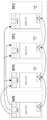
图1是现有技术中8口NVME硬盘背板点灯硬件示意图;Fig. 1 is the hardware schematic diagram of 8-port NVME hard disk backplane lighting hardware in the prior art;
图2是本发明实施例一中多个NVME硬盘背板级联方法的流程示意图;2 is a schematic flowchart of a method for cascading multiple NVME hard disk backplanes in
图3是本发明实际实施例中多个NVME硬盘背板点灯硬件示意图;3 is a schematic diagram of the lighting hardware of a plurality of NVME hard disk backplanes in an actual embodiment of the present invention;
图4是本发明实际实施例中主板与3个NVME硬盘背板级联的硬件示意图;Fig. 4 is the hardware schematic diagram of mainboard and 3 NVME hard disk backplanes cascade connection in the practical embodiment of the present invention;
图5是本发明实际实施例中向第一I2C中继器发送使能信号的流程示意图;5 is a schematic flowchart of sending an enable signal to a first I2C repeater in an actual embodiment of the present invention;
图6是本发明实际实施例中的查询对应关系表;6 is a query correspondence table in an actual embodiment of the present invention;
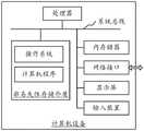
图7为本发明实施例二中多个NVME硬盘背板级联系统的结构框图;7 is a structural block diagram of a plurality of NVME hard disk backplane cascading systems in
图8为本发明实施例二中计算机设备的内部结构图。FIG. 8 is an internal structural diagram of a computer device in
具体实施方式Detailed ways
现有技术中,用于插接NVMe SSD(即NVME硬盘)的背板端需要通过LED灯来显示对应接口上的NVMe SSD的状态,而这个状态可由服务器主板CPU通过VPP接口连接背板、对背板进行点灯操作来实现。In the prior art, the backplane end used for plugging in the NVMe SSD (ie, the NVME hard disk) needs to display the status of the NVMe SSD on the corresponding interface through LED lights, and this status can be connected by the server motherboard CPU through the VPP interface The back panel performs a lighting operation to achieve this.
如图1所示,以8口NVME硬盘背板为例,现有服务器通过主板的4个MCIO/Slimline连接器与背板的MCIO/Slimline连接器连接;每个连接器的Sideband中,使用6个VPP地址信号。As shown in Figure 1, taking the 8-port NVME hard disk backplane as an example, the existing server is connected to the MCIO/Slimline connector on the backplane through the 4 MCIO/Slimline connectors on the motherboard; in the Sideband of each connector, 6 VPP address signal.
NVME背板上的Sideband连接器需要连接2组VPP信号到CPLD(ComplexProgrammable Logic Device,即复杂可编程逻辑器件);同时需要有一组I2C信号连接到I2C Repeater(即I2C中继器)到CPLD,与之对应的主板上也需要一个Sideband连接器连接到一个背板,每个背板都需要一个线缆连接主板和背板的两个Sideband连接器。The Sideband connector on the NVME backplane needs to connect 2 sets of VPP signals to CPLD (Complex Programmable Logic Device); at the same time, a set of I2C signals need to be connected to I2C Repeater (ie I2C repeater) to CPLD, and The corresponding motherboard also needs a Sideband connector to connect to a backplane, and each backplane requires a cable to connect the two Sideband connectors on the motherboard and the backplane.
NVME背板通过MCIO/Slimline连接器由主板获得VPP地址信号,同时再由VPP总线发送点灯信号给背板CPLD,CPLD解析主板CPU发出的VPP信号,然后与设定好的PCIE PortID表对比,从而完成点灯动作。The NVME backplane obtains the VPP address signal from the motherboard through the MCIO/Slimline connector, and at the same time sends the lighting signal to the backplane CPLD through the VPP bus. The CPLD parses the VPP signal sent by the motherboard CPU, and then compares it with the set PCIE PortID table. Complete the lighting action.
通过背板Sideband连接器上的BMC I2C,主板BMC可以进行CPLD信息读取、背板CPLD FW升级、背板温度及板卡PCBA及PCB等信息读取等操作。Through the BMC I2C on the sideband connector of the backplane, the mainboard BMC can perform operations such as CPLD information reading, backplane CPLD FW upgrade, backplane temperature, and information reading of board PCBA and PCB.
在实际使用中,上述8口NVME硬盘背板点灯技术方案存在以下缺点:In actual use, the above-mentioned 8-port NVME hard disk backplane lighting technical solution has the following disadvantages:
1.当前服务器连接NVME背板配置,每个主板MCIO/Slimline连接器用6个GPIO(General-purpose input/output,即通用型之输入/输出)传递给背板VPP地址信息,主板端占用大量MCIO/Slimline连接器管脚,同时背板端占用大量MCIO/Slimline连接器管脚及CPLD管脚;1. The current server is connected to the NVME backplane configuration. Each motherboard MCIO/Slimline connector uses 6 GPIOs (General-purpose input/output, that is, general-purpose input/output) to transmit the backplane VPP address information, and the motherboard side occupies a lot of MCIO /Slimline connector pins, while the backplane side occupies a large number of MCIO/Slimline connector pins and CPLD pins;
2.每个背板都需要一个线缆连接主板和背板的两个Sideband连接器,造成了连接主板的VPP和I2C资源增加,同时增加了主板连接器的数量;2. Each backplane needs a cable to connect the motherboard and the two Sideband connectors on the backplane, which increases the VPP and I2C resources connecting the motherboard and increases the number of motherboard connectors;
3.主板上的MCIO/Slimline连接器为了兼容PCIE X4、X8、X16及CPU Balance等多种配置要求,需要使用多个Sideband管脚;3. The MCIO/Slimline connector on the motherboard needs to use multiple Sideband pins in order to be compatible with various configuration requirements such as PCIE X4, X8, X16 and CPU Balance;
4.在多个背板进行级联时,不仅需要使用背板和主板大量连接器管脚资源、需要增加主板和背板Layout的布线,同时会增加线缆内部的信号数量。4. When multiple backplanes are cascaded, it is not only necessary to use a large number of connector pin resources on the backplane and the main board, but also to increase the wiring of the main board and the backplane layout, and at the same time, it will increase the number of signals inside the cable.
即,现有技术的服务器多个NVME背板点灯方案中,存在占用MCIO/Slimline连接器管脚及CPLD管脚的资源较多,因而造成相关资源不足以及导致相关资源成本增加等问题。That is, in the multiple NVME backplane lighting solutions for servers in the prior art, many resources are occupied by MCIO/Slimline connector pins and CPLD pins, resulting in insufficient related resources and increased related resource costs.
为此,本发明提供一种多个NVME硬盘背板级联方法、系统、设备及介质,用来解决上述问题。To this end, the present invention provides a method, system, device and medium for cascading multiple NVME hard disk backplanes to solve the above problems.
为使本发明的目的、技术方案和优点更加清楚,下面将结合本发明实施例中的附图,对本发明实施例中的技术方案进行清楚、完整地描述,显然,所描述的实施例仅仅是本发明一部分实施例,而不是全部的实施例。基于本发明中的实施例,本领域普通技术人员在没有做出创造性劳动前提下所获得的所有其它实施例,都属于本发明保护的范围。In order to make the objectives, technical solutions and advantages of the present invention clearer, the technical solutions in the embodiments of the present invention will be clearly and completely described below with reference to the accompanying drawings in the embodiments of the present invention. Obviously, the described embodiments are only Some, but not all, embodiments of the present invention. Based on the embodiments of the present invention, all other embodiments obtained by those of ordinary skill in the art without creative efforts shall fall within the protection scope of the present invention.
实施例一:Example 1:
如图2所示,本发明实施例提供一种多个NVME硬盘背板级联方法,包括:As shown in FIG. 2, an embodiment of the present invention provides a method for cascading multiple NVME hard disk backplanes, including:
S1:将主板与多个NVME硬盘背板依次按菊花链形式进行级联,对每个NVME硬盘背板设置唯一的背板地址;S1: cascade the mainboard and multiple NVME hard disk backplanes in sequence in a daisy-chain form, and set a unique backplane address for each NVME hard disk backplane;
S2:将NVME硬盘背板配置信息与各个背板地址以及各个背板虚拟接口地址建立查询对应关系;其中,NVME硬盘背板配置信息包括背板识别信号数量、NVME硬盘背板数量;S2: Establish a query correspondence between the NVME hard disk backplane configuration information and each backplane address and each backplane virtual interface address; wherein, the NVME hard disk backplane configuration information includes the number of backplane identification signals and the number of NVME hard disk backplanes;
S4:当背板CPLD获取到当前背板地址时,根据查询对应关系查询得到当前背板虚拟接口地址,并解析当前背板虚拟接口地址得到对应的虚拟接口点灯信号。S4: When the backplane CPLD obtains the current backplane address, the current backplane virtual interface address is queried according to the query corresponding relationship, and the current backplane virtual interface address is parsed to obtain the corresponding virtual interface lighting signal.
在具体实施例中,每个NVME硬盘背板设有唯一的背板地址(即BP_ADDR),可通过背板地址来区分各个NVME硬盘背板;In a specific embodiment, each NVME hard disk backplane is provided with a unique backplane address (ie BP_ADDR), and each NVME hard disk backplane can be distinguished by the backplane address;
预先将背板识别信号(即BP_DETECT)数量、NVME硬盘背板数量、各个背板地址以及各个背板虚拟接口地址四者建立查询对应关系,查询对应关系可以是对应关系表格,用来根据某个已知信息查询其他信息;Establish a query corresponding relationship among the number of backplane identification signals (ie BP_DETECT), the number of NVME hard disk backplanes, each backplane address, and each backplane virtual interface address in advance. Known information to query other information;
当需要进行点灯操作时,NVME硬盘背板中的背板CPLD可先获取当前背板地址,再根据此查询对应关系来查询当前背板虚拟接口地址,从而再解析当前背板虚拟接口地址得到对应的虚拟接口点灯信号,用来控制点灯操作、实现NVME硬盘背板的点灯功能;When the lighting operation is required, the backplane CPLD in the backplane of the NVME hard disk can first obtain the current backplane address, and then query the current backplane virtual interface address according to the corresponding query relationship, so as to parse the current backplane virtual interface address to obtain the corresponding The virtual interface lighting signal is used to control the lighting operation and realize the lighting function of the NVME hard disk backplane;
其中,主板与NVME硬盘背板进行级联,可以节省多个主板与背板MCIO/SLIMLINE连接器管脚以及Sideband连接器,同时可以节省CPLD的管脚资源;Among them, the main board and the NVME hard disk backplane are cascaded, which can save multiple main board and backplane MCIO/SLIMLINE connector pins and Sideband connectors, and can save the pin resources of CPLD;
建立查询关系、解析得到对应的虚拟接口点灯信号后,可完成该背板的NVME硬盘点灯功能,同时可减少管脚资源的占用。After the query relationship is established and the corresponding virtual interface lighting signal is obtained by analysis, the lighting function of the NVME hard disk of the backplane can be completed, and the occupation of pin resources can be reduced at the same time.
如图4所示,在实际实施例中,主板可与3个NVME硬盘背板进行菊花链形式的级联:As shown in Figure 4, in an actual embodiment, the main board can be cascaded in a daisy-chain form with three NVME hard disk backplanes:
主板的一个Sideband连接器连接BMC I2C以及VPP信号可以连接三个背板的Sideband连接器,同时通过该Sideband连接器的BP_ADDR地址区分级联背板的配置信息;这样,可以节省多个主板与背板MCIO/SLIMLINE CONN管脚以及Sideband连接器,同时可以节省CPLD的管脚资源。One sideband connector of the mainboard is connected to BMC I2C and VPP signals, and can be connected to the sideband connectors of three backplanes. At the same time, the configuration information of the cascaded backplane can be distinguished by the BP_ADDR address of the sideband connector; in this way, multiple mainboards and backplanes can be saved. The board MCIO/SLIMLINE CONN pins and Sideband connectors can save the pin resources of CPLD.
如图6所示,在实际实施例中,背板BP_DETECT信号数量、NVME硬盘背板数量、各个BP_ADDR背板地址以及各个背板VPP地址四者可建立查询对应关系表,用于根据某个已知信息查询其他信息。As shown in FIG. 6, in an actual embodiment, the number of backplane BP_DETECT signals, the number of NVME hard disk backplanes, each BP_ADDR backplane address, and each backplane VPP address can establish a query correspondence table, which can be used according to a certain information to inquire about other information.
在一个优选的实施方式中,前述方法还包括:In a preferred embodiment, the aforementioned method further comprises:
S51:通过背板IO扩展器获取当前背板地址;S51: Obtain the current backplane address through the backplane IO expander;
S52:通过背板管理控制器的I2C信号控制背板IO扩展器向第一I2C中继器发送使能信号;其中,第一I2C中继器与当前背板地址对应的NVME硬盘背板相匹配。S52: Control the backplane IO expander to send an enable signal to the first I2C repeater through the I2C signal of the backplane management controller; wherein the first I2C repeater matches the NVME hard disk backplane corresponding to the current backplane address .
在具体实施例中,通过IO扩展器(即IO Expander)和CPLD对背板地址的复用及背板地址在多个背板的级联,可节省较多的高速连接器的Sideband管脚;In a specific embodiment, the multiplexing of the backplane address by the IO expander (that is, the IO Expander) and the CPLD and the cascading of the backplane address on a plurality of backplanes can save more Sideband pins of the high-speed connector;
此外,背板BMC(即背板管理控制器)通过I2C控制IO Expander信号使能对应背板I2C Repeater,可减少不必要的I2C支路对信号质量的影响;同时由于减少了不必要的I2C设备接入,从而可提高BMC中I2C轮询的效率。In addition, the backplane BMC (that is, the backplane management controller) controls the IO Expander signal through the I2C to enable the corresponding backplane I2C Repeater, which can reduce the impact of unnecessary I2C branches on signal quality; at the same time, because unnecessary I2C devices are reduced access, thereby improving the efficiency of I2C polling in the BMC.
在一个优选的实施方式中,在背板管理控制器通过I2C信号控制背板IO扩展器向第一I2C中继器发送使能信号之前,前述方法还包括:In a preferred embodiment, before the backplane management controller controls the backplane IO expander to send the enable signal to the first I2C repeater through the I2C signal, the aforementioned method further includes:
背板管理控制器通过I2C信号读取第一I2C中继器的使能Pin引脚电平;The backplane management controller reads the enabled Pin pin level of the first I2C repeater through the I2C signal;
若使能Pin引脚电平为高电平,则使能控制设置成功;If the level of the enable Pin pin is high, the enable control setting is successful;
若使能Pin引脚电平不是高电平,则背板管理控制器通过I2C信号重新控制背板IO扩展器向第一I2C中继器发送使能信号。If the level of the enable Pin pin is not a high level, the backplane management controller re-controls the backplane IO expander to send the enable signal to the first I2C repeater through the I2C signal.
如图5所示,在实际实施例中,服务器主板BMC可控制背板IO Expander向第一I2C中继器发送使能信号。As shown in FIG. 5 , in an actual embodiment, the server motherboard BMC can control the backplane IO Expander to send an enable signal to the first I2C repeater.
其中,为了验证使能控制是否设置成功,主板BMC读取IO Expander的使能IO电平状态;如果是高则设置成功;否则重新进入设置I2C Repeater使能流程,重复5次仍然不成功,BMC则记录相关报错日志,结束流程。Among them, in order to verify whether the enable control is set successfully, the motherboard BMC reads the enabled IO level status of the IO Expander; if it is high, the setting is successful; otherwise, it re-enters the setting of the I2C Repeater enable process, and repeats 5 times still unsuccessful, BMC Then record the relevant error log and end the process.
在一个优选的实施方式中,前述方法还包括:In a preferred embodiment, the aforementioned method further comprises:
S53:背板IO Expander向第二I2C中继器发送使能信号;其中,第二I2C中继器用于接收CPU虚拟接口信号并发送至背板CPLD。S53: The backplane IO Expander sends an enable signal to the second I2C repeater; wherein the second I2C repeater is used to receive the CPU virtual interface signal and send it to the backplane CPLD.
较佳的,背板上Sideband连接器上的BMC I2C和CPU虚拟接口信号级联,可极大减少主板上Sideband连接器的数量。Preferably, the BMC I2C and CPU virtual interface signals on the sideband connector on the backplane are cascaded, which can greatly reduce the number of sideband connectors on the motherboard.
在一个优选的实施方式中,在背板CPLD获取当前背板地址之前,前述方法还包括:In a preferred embodiment, before the backplane CPLD acquires the current backplane address, the aforementioned method further includes:
S31:主板监测当前识别信号数量,并根据查询对应关系查询得到当前NVME硬盘背板数量以及当前背板地址。S31: The main board monitors the current number of identification signals, and obtains the current number of NVME hard disk backplanes and the current backplane address according to the query corresponding relationship.
在具体实施例中,按照不同服务器的配置需要级联的NVME背板数量,给出对应的CPLD端可以侦测到的BP_DETECT信号数量。主板通过侦测BP_DETECT信号数量就可以知道现有配置连接NVME背板的数量及类型,从而BMC可以查表(即查询对应关系)得到每个级联背板对应的BP_ADDR对应关系。In a specific embodiment, the number of BP_DETECT signals that can be detected by the corresponding CPLD end is given according to the number of NVME backplanes that need to be cascaded according to the configuration of different servers. The mainboard can know the number and type of NVME backplanes connected to the existing configuration by detecting the number of BP_DETECT signals, so that the BMC can look up the table (that is, query the correspondence) to obtain the corresponding BP_ADDR correspondence of each cascaded backplane.
在一个优选的实施方式中,前述方法还包括:In a preferred embodiment, the aforementioned method further comprises:
S32:将主板CPU的PCIE X8信号分配为X4信号。S32: Assign the PCIE X8 signal of the motherboard CPU to the X4 signal.
较佳的,NVME硬盘(PCIE X4)的读写速率较高,更适用于数据高速存储及数据高速读取。Preferably, the NVME hard disk (PCIE X4) has a higher read and write rate, and is more suitable for high-speed data storage and high-speed data reading.
在实际实施例中,如图3所示,对现有技术方案进行改善后,多个NVME硬盘背板点灯硬件系统具体包括如下:In an actual embodiment, as shown in FIG. 3 , after improving the existing technical solution, a plurality of NVME hard disk backplane lighting hardware systems specifically include the following:
MCIO/SLIMLINE CONN:主板与背板PCIE及BP_DETECT信号传输的连接器,按照整机NVME硬盘配置不同每个连接器与背板连接器对应关系一一对应;MCIO/SLIMLINE CONN: The connector for PCIE and BP_DETECT signal transmission between the motherboard and the backplane. According to the different NVME hard disk configuration of the whole machine, the corresponding relationship between each connector and the backplane connector corresponds one by one;
BP_ADDR:主板端为下拉,NVME背板端为若上拉,通过Cable互连不同进行设置每个背板的三位BP_ADDR地址来区分三个不同的背板;若没有连接到主板端CPLD,则为三位高电平,为IO Expander及CPLD提供地址电平;BP_ADDR: The main board side is pulled down, and the NVME backplane side is pulled up. Set the three-bit BP_ADDR address of each backplane to distinguish three different backplanes through different cable interconnections; if it is not connected to the mainboard side CPLD, then It is three high level, providing address level for IO Expander and CPLD;
Sideband Conn:主板与背板Sideband信号(CPU_VPP/BMC_I2C/BP_ADDR信号)传输的连接器;Sideband Conn: The connector for transmitting sideband signals (CPU_VPP/BMC_I2C/BP_ADDR signals) between the motherboard and the backplane;
I2C Repeater芯片:带有使能Pin脚的I2C中继芯片;在图1中,使能Pin固定连接到使能状态;如图3和图4所示,该使能信号由BMC的I2C总线IO Expander进行控制,控制该背板的I2C Repeater是否导通,该Pin默认状态为非使能;I2C Repeater chip: an I2C repeater chip with an enable pin; in Figure 1, the enable Pin is fixedly connected to the enable state; as shown in Figure 3 and Figure 4, the enable signal is provided by the I2C bus IO of the BMC The Expander controls whether the I2C Repeater of the backplane is turned on. The default state of the Pin is disabled;
IO Expander:在图1中该芯片的地址为固定地址;如图3和图4所示,该芯片地址与CPLD共用BP_ADDR,同时增加一位使能信号连接到BMC_I2C和CPU_VPP的I2C Repeater芯片的使能Pin脚;BMC通过I2C访问BP_ADDR地址,控制背板的I2C Repeater使能;IO Expander: In Figure 1, the address of the chip is a fixed address; as shown in Figure 3 and Figure 4, the chip address shares BP_ADDR with CPLD, and an enable signal is added to connect to the I2C Repeater chip of BMC_I2C and CPU_VPP. Can Pin; BMC accesses the BP_ADDR address through I2C, and controls the I2C Repeater enable on the backplane;
CPLD:解析主板传输的CPU_VPP及BP_ADDR信号完成硬盘点灯功能,可以接收并解析BMC发出的读写信息、并可以完成CPLD FW的升级。CPLD: Analyze the CPU_VPP and BP_ADDR signals transmitted by the motherboard to complete the hard disk lighting function, receive and analyze the read and write information sent by the BMC, and complete the CPLD FW upgrade.
本发明实际实施例中,多个NVME硬盘背板级联后,可实现如下功能:In the actual embodiment of the present invention, after multiple NVME hard disk backplanes are cascaded, the following functions can be implemented:
如图3、图5所示,背板端的每个MCIO/SLIMLINE CONN的BP_DETECT信号通过电阻连接到地、并传递给主板,主板CPLD通过侦测MCIO/SLIMLINE CONN的BP_DETECT信号可以知道后端连接的是NVME背板,并将连接器上行PCIE X8信号分配为X4。As shown in Figure 3 and Figure 5, the BP_DETECT signal of each MCIO/SLIMLINE CONN on the backplane is connected to the ground through a resistor and transmitted to the main board. The main board CPLD can know the back-end connection by detecting the BP_DETECT signal of the MCIO/SLIMLINE CONN. Is the NVME backplane and assigns the connector upstream PCIE X8 signal to X4.
如图5、图6所示,按照不同服务器的配置需要级联的NVME背板数量,给出对应的CPLD端可以侦测到的BP_DETECT信号数量。主板通过侦测BP_DETECT信号数量就可以知道现有配置连接NVME背板的数量及类型,从而BMC可以查表得到每个级联背板对应的BP_ADDR对应关系,进一步BMC通过I2C控制背板IO Expander的使能IO打开对应背板的I2C Repeater;As shown in Figure 5 and Figure 6, according to the number of NVME backplanes that need to be cascaded according to the configuration of different servers, the number of BP_DETECT signals that can be detected by the corresponding CPLD end is given. The mainboard can know the number and type of NVME backplanes connected to the existing configuration by detecting the number of BP_DETECT signals, so that the BMC can look up the table to obtain the corresponding relationship of BP_ADDR for each cascaded backplane. Further, the BMC controls the backplane IO Expander through I2C. Enable IO to open the I2C Repeater corresponding to the backplane;
为了检测上述使能控制是否设置成功,主板BMC读取IO Expander的使能IO电平状态;如果是高则设置成功;否则重新进入设置I2C Repeater使能流程,重复5次仍然不成功,BMC记录相关报错日志,结束流程。In order to detect whether the above enable control is successfully set, the main board BMC reads the enabled IO level status of the IO Expander; if it is high, the setting is successful; otherwise, it re-enters the setting of the I2C Repeater enable process, and repeats 5 times and still fails, BMC records Relevant error log, end the process.
如图4、图6所示,8NVME背板级联配置和对应的背板地址和VPPADDR呈对应关系,背板端CPLD通过解析三位BP_ADDR信号,可以知道当前背板的VPP地址信息,进而可以通过解析对应的VPP点灯信号,完成该背板的NVME硬盘点灯功能。As shown in Figure 4 and Figure 6, the 8NVME backplane cascade configuration is in a corresponding relationship with the corresponding backplane address and VPPADDR. By analyzing the three-bit BP_ADDR signal, the CPLD on the backplane can know the VPP address information of the current backplane, and then can By analyzing the corresponding VPP lighting signal, the NVME hard disk lighting function of the backplane is completed.
同时,按照8NVME背板级联配置和对应的背板地址和VPPADDR对应关系,BMC可以按照对应的BP_ADDR读取IO Expander上的PCBA及PCB等信息。At the same time, according to the 8NVME backplane cascade configuration and the corresponding relationship between the backplane address and VPPADDR, the BMC can read the PCBA and PCB information on the IO Expander according to the corresponding BP_ADDR.
在实际中,为实现上述多个NVME硬盘背板级联方法,可采用如下步骤来实现:In practice, in order to realize the above-mentioned method of cascading multiple NVME hard disk backplanes, the following steps can be used:
1)按照图3评估主板和背板CPLD管脚数量及逻辑需求数量,选择适用的CPLD型号,评估IO Expander芯片管脚数量,选用适当的IO Expander芯片;1) According to Figure 3, evaluate the number of CPLD pins and logic requirements on the main board and backplane, select the appropriate CPLD model, evaluate the number of pins of the IO Expander chip, and select the appropriate IO Expander chip;
2)按照图3对主板和背板进行硬件设计,将IO Expander及I2C Repeater芯片靠近Sideband连接器;2) Carry out hardware design for the main board and backplane according to Figure 3, and place the IO Expander and I2C Repeater chips close to the Sideband connector;
3)按照图4所示级联方式进行线缆设计、并进行多个背板连接;3) Design the cables according to the cascading method shown in Figure 4, and perform multiple backplane connections;
4)按照图5和图6所示,整理不同配置下NVME背板MCIO/SLIMLINE CONN的BP_DETECT数量,梳理出配置中的背板数量及对应的BP_ADDR和VPP地址,按照配置数量不同通过BMC I2C控制IO Expander的使能管脚来控制对应的I2C通路,减少I2C分叉长度,提高I2C信号质量;4) As shown in Figure 5 and Figure 6, sort out the number of BP_DETECTs of the NVME backplane MCIO/SLIMLINE CONN under different configurations, sort out the number of backplanes in the configuration and the corresponding BP_ADDR and VPP addresses, and control them through BMC I2C according to the number of configurations The enable pin of the IO Expander is used to control the corresponding I2C path, reduce the length of the I2C bifurcation, and improve the quality of the I2C signal;
5)按照图6所示,按照背板CPLD逻辑流程进行BP_ADDR和VPP地址对应关系设计,同时将BMC对应读取NVME背板的IO Expander地址对应关系进行更新。5) As shown in FIG. 6 , design the corresponding relationship between BP_ADDR and VPP address according to the backplane CPLD logic flow, and at the same time update the corresponding relationship of the IO Expander address corresponding to the BMC reading the NVME backplane.
综上,本发明实施例提供的一种多个NVME硬盘背板级联方法,具有以下有益效果:In conclusion, a method for cascading multiple NVME hard disk backplanes provided by the embodiment of the present invention has the following beneficial effects:
主板CPLD逻辑按照服务器配置与背板地址及VPP地址对应表格;The motherboard CPLD logic corresponds to the backplane address and VPP address according to the server configuration;
BMC通过I2C控制IO Expander信号使能对应背板I2C Repeater,减少了不必要的I2C支路对信号质量的影响,同时由于减少了不必要的I2C设备接入,提高了BMC I2C轮询的效率;BMC controls the IO Expander signal through I2C to enable the corresponding backplane I2C Repeater, which reduces the impact of unnecessary I2C branches on signal quality, and at the same time reduces unnecessary I2C device access, improving the efficiency of BMC I2C polling;
通过IO Expander和CPLD对背板地址的复用及背板地址在多个背板的级联,节省了较多的高速连接器的Sideband管脚;The multiplexing of backplane addresses by IO Expander and CPLD and the cascading of backplane addresses on multiple backplanes saves more Sideband pins of high-speed connectors;
同时背板上Sideband连接器上的BMC I2C和CPU VPP信号级联,大大地减少了主板上Sideband连接器的数量。At the same time, the BMC I2C and CPU VPP signals on the Sideband connector on the backplane are cascaded, which greatly reduces the number of Sideband connectors on the motherboard.
由此,可有效解决现有服务器多个NVME背板与主板连接过程中占用MCIO/Slimline/Sideband连接器管脚、以及CPLD管脚资源较多,导致相关资源不足、增加相关资源成本的技术问题。As a result, it can effectively solve the technical problem that many MCIO/Slimline/Sideband connector pins and CPLD pin resources are occupied in the process of connecting multiple NVME backplanes of the existing server to the main board, resulting in insufficient related resources and increased related resource costs. .
需要注意的是,虽然流程图中的各个步骤按照箭头的指示依次显示,但是这些步骤并不是必然按照箭头指示的顺序依次执行。除非本文中有明确的说明,这些步骤的执行并没有严格的顺序限制,这些步骤可以以其它的顺序执行。而且,流程图中的至少一部分步骤可以包括多个子步骤或者多个阶段,这些子步骤或者阶段并不必然是在同一时刻执行完成,而是可以在不同的时刻执行,这些子步骤或者阶段的执行顺序也不必然是依次进行,而是可以与其它步骤或者其它步骤的子步骤或者阶段的至少一部分轮流或者交替地执行。It should be noted that although the steps in the flowchart are displayed in sequence according to the arrows, these steps are not necessarily executed in the sequence indicated by the arrows. Unless explicitly stated herein, the execution of these steps is not strictly limited to the order, and these steps may be performed in other orders. Moreover, at least a part of the steps in the flowchart may include multiple sub-steps or multiple stages. These sub-steps or stages are not necessarily executed at the same time, but may be executed at different times. The execution of these sub-steps or stages The sequence is also not necessarily sequential, but may be performed alternately or alternately with other steps or sub-steps of other steps or at least a portion of a phase.
实施例二:Embodiment 2:
如图7所示,本发明实施例还提供一种多个NVME硬盘背板级联系统,基于前述的多个NVME硬盘背板级联方法,系统包括:As shown in FIG. 7 , an embodiment of the present invention further provides a system for cascading multiple NVME hard disk backplanes. Based on the foregoing method for cascading multiple NVME hard disk backplanes, the system includes:
级联模块1,用于将主板与多个NVME硬盘背板依次按菊花链形式进行级联;
背板地址设置模块2,用于对每个NVME硬盘背板设置唯一的背板地址;Backplane
关系建立模块3,用于将NVME硬盘背板配置信息与各个背板地址以及各个背板虚拟接口地址建立查询对应关系;其中,NVME硬盘背板配置信息包括背板识别信号数量、NVME硬盘背板数量;The
查询解析模块4,用于当背板CPLD获取到当前背板地址后,根据查询对应关系查询得到当前背板虚拟接口地址,并解析当前背板虚拟接口地址得到对应的虚拟接口点灯信号。The query and
在一个优选的实施方式中,前述系统还包括:In a preferred embodiment, the aforementioned system further comprises:
背板地址获取模块,用于通过背板IO扩展器获取当前背板地址;The backplane address acquisition module is used to acquire the current backplane address through the backplane IO expander;
使能信号发送控制模块,用于通过背板管理控制器的I2C信号控制背板IO扩展器向第一I2C中继器发送使能信号;其中,第一I2C中继器与当前背板地址对应的NVME硬盘背板相匹配。The enable signal sending control module is used to control the backplane IO expander to send the enable signal to the first I2C repeater through the I2C signal of the backplane management controller; wherein, the first I2C repeater corresponds to the current backplane address NVME HDD backplane to match.
在一个优选的实施方式中,前述系统还包括验证使能控制模块,用于通过背板管理控制器通过I2C信号读取第一I2C中继器的使能Pin引脚电平;在使能Pin引脚电平为高电平时验证使能控制设置成功;In a preferred embodiment, the aforementioned system further includes a verification enable control module for reading the enable Pin level of the first I2C repeater through the I2C signal through the backplane management controller; Verify that the enable control setting is successful when the pin level is high;
使能信号发送控制模块还用于在使能Pin引脚电平不是高电平时,通过背板管理控制器的I2C信号重新控制背板IO扩展器向第一I2C中继器发送使能信号。The enable signal sending control module is further configured to re-control the backplane IO expander to send the enable signal to the first I2C repeater through the I2C signal of the backplane management controller when the level of the enable Pin pin is not high.
在一个优选的实施方式中,使能信号发送控制模块还用于控制背板IO扩展器向第二I2C中继器发送使能信号;其中,第二I2C中继器用于接收CPU_虚拟接口信号并发送至背板CPLD。In a preferred embodiment, the enable signal sending control module is further configured to control the backplane IO expander to send an enable signal to the second I2C repeater; wherein the second I2C repeater is configured to receive the CPU_virtual interface signal And sent to the backplane CPLD.
在一个优选的实施方式中,前述系统还包括背板查询模块,用于在主板监测到当前识别信号数量时,根据查询对应关系查询得到当前NVME硬盘背板数量以及当前背板地址。In a preferred embodiment, the aforementioned system further includes a backplane query module for obtaining the current number of NVME hard disk backplanes and the current backplane address according to the query correspondence when the mainboard monitors the current number of identification signals.
在一个优选的实施方式中,前述系统还包括信号分配模块,用于将主板CPU的PCIEX8信号分配为X4信号。In a preferred embodiment, the aforementioned system further includes a signal distribution module for distributing the PCIEX8 signal of the motherboard CPU as the X4 signal.
关于多个NVME硬盘背板级联系统的具体限定,可以参见上文中对于多个NVME硬盘背板级联方法的限定,在此不再赘述。For the specific limitation of the system for cascading multiple NVME hard disk backplanes, reference may be made to the foregoing limitations on the method for cascading multiple NVME hard disk backplanes, which will not be repeated here.
上述系统中的各个模块,可全部或部分通过软件、硬件及其组合来实现。上述各模块可以以硬件形式内嵌于、或独立于计算机设备中的处理器中,也可以以软件形式存储于计算机设备中的存储器中,以便于处理器调用执行以上各个模块对应的操作。Each module in the above-mentioned system can be implemented in whole or in part by software, hardware and combinations thereof. The above modules can be embedded in or independent of the processor in the computer device in the form of hardware, or can be stored in the memory of the computer device in the form of software, so that the processor can call and execute the operations corresponding to the above modules.
其中,如图8所示,上述计算机设备可以是终端,其包括通过系统总线连接的处理器、存储器、网络接口、显示屏和输入装置。其中,该计算机设备的处理器用于提供计算和控制能力。该计算机设备的存储器包括非易失性存储介质、内存储器。该非易失性存储介质存储有操作系统和计算机程序。该内存储器为非易失性存储介质中的操作系统和计算机程序的运行提供环境。该计算机设备的网络接口用于与外部的终端通过网络连接通信。该计算机设备的显示屏可以是液晶显示屏或者电子墨水显示屏,该计算机设备的输入装置可以是显示屏上覆盖的触摸层,也可以是计算机设备外壳上设置的按键、轨迹球或触控板,还可以是外接的键盘、触控板或鼠标等。Wherein, as shown in FIG. 8 , the above-mentioned computer equipment may be a terminal, which includes a processor, a memory, a network interface, a display screen and an input device connected through a system bus. Among them, the processor of the computer device is used to provide computing and control capabilities. The memory of the computer device includes a non-volatile storage medium, an internal memory. The nonvolatile storage medium stores an operating system and a computer program. The internal memory provides an environment for the execution of the operating system and computer programs in the non-volatile storage medium. The network interface of the computer device is used to communicate with an external terminal through a network connection. The display screen of the computer equipment may be a liquid crystal display screen or an electronic ink display screen, and the input device of the computer equipment may be a touch layer covered on the display screen, or a button, a trackball or a touchpad set on the shell of the computer equipment , or an external keyboard, trackpad, or mouse.
可以理解的是,上述图中示出的结构,仅仅是与本发明方案相关的部分结构的框图,并不构成对本发明方案所应用于其上的计算机设备的限定,具体的计算机设备可以包括比图中所示更多或更少的部件,或者组合某些部件,或者具有不同的部件布置。It can be understood that the structure shown in the above figures is only a block diagram of a part of the structure related to the solution of the present invention, and does not constitute a limitation on the computer equipment to which the solution of the present invention is applied. More or fewer components are shown in the figures, either in combination or with different arrangements of components.
实施例三:Embodiment three:
本发明实施例又提供一种计算机设备,包括存储器、处理器及计算机程序,计算机程序存储在存储器上并可在处理器上运行,处理器执行计算机程序时实现以下步骤:An embodiment of the present invention further provides a computer device, including a memory, a processor, and a computer program, where the computer program is stored in the memory and can be run on the processor, and the processor implements the following steps when executing the computer program:
S1:将主板与多个NVME硬盘背板依次按菊花链形式进行级联,对每个NVME硬盘背板设置唯一的背板地址;S1: cascade the mainboard and multiple NVME hard disk backplanes in sequence in a daisy-chain form, and set a unique backplane address for each NVME hard disk backplane;
S2:将NVME硬盘背板配置信息与各个背板地址以及各个背板虚拟接口地址建立查询对应关系;其中,NVME硬盘背板配置信息包括背板识别信号数量、NVME硬盘背板数量;S2: Establish a query correspondence between the NVME hard disk backplane configuration information and each backplane address and each backplane virtual interface address; wherein, the NVME hard disk backplane configuration information includes the number of backplane identification signals and the number of NVME hard disk backplanes;
S4:当背板CPLD获取到当前背板地址时,根据查询对应关系查询得到当前背板虚拟接口地址,并解析当前背板虚拟接口地址得到对应的虚拟接口点灯信号。S4: When the backplane CPLD obtains the current backplane address, the current backplane virtual interface address is queried according to the query corresponding relationship, and the current backplane virtual interface address is parsed to obtain the corresponding virtual interface lighting signal.
在一个优选的实施方式中,处理器执行计算机程序时还实现以下步骤:In a preferred embodiment, the processor also implements the following steps when executing the computer program:
S51:通过背板IO扩展器获取当前背板地址;S51: Obtain the current backplane address through the backplane IO expander;
S52:通过背板管理控制器的I2C信号控制背板IO扩展器向第一I2C中继器发送使能信号;其中,第一I2C中继器与当前背板地址对应的NVME硬盘背板相匹配。S52: Control the backplane IO expander to send an enable signal to the first I2C repeater through the I2C signal of the backplane management controller; wherein the first I2C repeater matches the NVME hard disk backplane corresponding to the current backplane address .
在一个优选的实施方式中,处理器执行计算机程序时还实现以下步骤:In a preferred embodiment, the processor also implements the following steps when executing the computer program:
在背板管理控制器通过I2C信号控制背板IO扩展器向第一I2C中继器发送使能信号之前,背板管理控制器通过I2C信号读取第一I2C中继器的使能Pin引脚电平;若使能Pin引脚电平为高电平,则使能控制设置成功;若使能Pin引脚电平不是高电平,则背板管理控制器通过I2C信号重新控制背板IO扩展器向第一I2C中继器发送使能信号。Before the backplane management controller controls the backplane IO expander to send the enable signal to the first I2C repeater through the I2C signal, the backplane management controller reads the enable Pin of the first I2C repeater through the I2C signal level; if the enable pin level is high, the enable control setting is successful; if the enable pin level is not high, the backplane management controller re-controls the backplane IO through the I2C signal The expander sends an enable signal to the first I2C repeater.
在一个优选的实施方式中,处理器执行计算机程序时还实现以下步骤:In a preferred embodiment, the processor also implements the following steps when executing the computer program:
S53:背板IO扩展器向第二I2C中继器发送使能信号;其中,第二I2C中继器用于接收CPU_虚拟接口信号并发送至背板CPLD。S53: The backplane IO expander sends an enable signal to the second I2C repeater, wherein the second I2C repeater is used to receive the CPU_virtual interface signal and send it to the backplane CPLD.
在一个优选的实施方式中,处理器执行计算机程序时还实现以下步骤:In a preferred embodiment, the processor also implements the following steps when executing the computer program:
在背板CPLD获取当前背板地址之前,实现步骤S31:主板监测当前识别信号数量,并根据查询对应关系查询得到当前NVME硬盘背板数量以及当前背板地址。Before the backplane CPLD obtains the current backplane address, step S31 is implemented: the main board monitors the current number of identification signals, and obtains the current number of NVME hard disk backplanes and the current backplane address according to the query corresponding relationship.
在一个优选的实施方式中,处理器执行计算机程序时还实现以下步骤:In a preferred embodiment, the processor also implements the following steps when executing the computer program:
S32:将主板CPU的PCIE X8信号分配为X4信号。S32: Assign the PCIE X8 signal of the motherboard CPU to the X4 signal.
实施例四:Embodiment 4:
本发明实施例再提供一种计算机可读存储介质,存储有计算机程序,计算机程序被处理器执行时实现以下步骤:An embodiment of the present invention further provides a computer-readable storage medium, which stores a computer program, and when the computer program is executed by a processor, implements the following steps:
S1:将主板与多个NVME硬盘背板依次按菊花链形式进行级联,对每个NVME硬盘背板设置唯一的背板地址;S1: cascade the mainboard and multiple NVME hard disk backplanes in sequence in a daisy-chain form, and set a unique backplane address for each NVME hard disk backplane;
S2:将NVME硬盘背板配置信息与各个背板地址以及各个背板虚拟接口地址建立查询对应关系;其中,NVME硬盘背板配置信息包括背板识别信号数量、NVME硬盘背板数量;S2: Establish a query correspondence between the NVME hard disk backplane configuration information and each backplane address and each backplane virtual interface address; wherein, the NVME hard disk backplane configuration information includes the number of backplane identification signals and the number of NVME hard disk backplanes;
S4:当背板CPLD获取到当前背板地址时,根据查询对应关系查询得到当前背板虚拟接口地址,并解析当前背板虚拟接口地址得到对应的虚拟接口点灯信号。S4: When the backplane CPLD obtains the current backplane address, the current backplane virtual interface address is queried according to the query corresponding relationship, and the current backplane virtual interface address is parsed to obtain the corresponding virtual interface lighting signal.
在一个优选的实施方式中,计算机程序被处理器执行时还实现以下步骤:In a preferred embodiment, the computer program further implements the following steps when executed by the processor:
S51:通过背板IO扩展器获取当前背板地址;S51: Obtain the current backplane address through the backplane IO expander;
S52:通过背板管理控制器的I2C信号控制背板IO扩展器向第一I2C中继器发送使能信号;其中,第一I2C中继器与当前背板地址对应的NVME硬盘背板相匹配。S52: Control the backplane IO expander to send an enable signal to the first I2C repeater through the I2C signal of the backplane management controller; wherein the first I2C repeater matches the NVME hard disk backplane corresponding to the current backplane address .
在一个优选的实施方式中,计算机程序被处理器执行时还实现以下步骤:In a preferred embodiment, the computer program further implements the following steps when executed by the processor:
在背板管理控制器通过I2C信号控制背板IO扩展器向第一I2C中继器发送使能信号之前,背板管理控制器通过I2C信号读取第一I2C中继器的使能Pin引脚电平;若使能Pin引脚电平为高电平,则使能控制设置成功;若使能Pin引脚电平不是高电平,则背板管理控制器通过I2C信号重新控制背板IO扩展器向第一I2C中继器发送使能信号。Before the backplane management controller controls the backplane IO expander to send the enable signal to the first I2C repeater through the I2C signal, the backplane management controller reads the enable Pin of the first I2C repeater through the I2C signal level; if the enable pin level is high, the enable control setting is successful; if the enable pin level is not high, the backplane management controller re-controls the backplane IO through the I2C signal The expander sends an enable signal to the first I2C repeater.
在一个优选的实施方式中,计算机程序被处理器执行时还实现以下步骤:In a preferred embodiment, the computer program further implements the following steps when executed by the processor:
S53:背板IO扩展器向第二I2C中继器发送使能信号;其中,第二I2C中继器用于接收CPU_虚拟接口信号并发送至背板CPLD。S53: The backplane IO expander sends an enable signal to the second I2C repeater, wherein the second I2C repeater is used to receive the CPU_virtual interface signal and send it to the backplane CPLD.
在一个优选的实施方式中,计算机程序被处理器执行时还实现以下步骤:In a preferred embodiment, the computer program further implements the following steps when executed by the processor:
在背板CPLD获取当前背板地址之前,实现步骤S31:主板监测当前识别信号数量,并根据查询对应关系查询得到当前NVME硬盘背板数量以及当前背板地址。Before the backplane CPLD obtains the current backplane address, step S31 is implemented: the main board monitors the current number of identification signals, and obtains the current number of NVME hard disk backplanes and the current backplane address according to the query corresponding relationship.
在一个优选的实施方式中,计算机程序被处理器执行时还实现以下步骤:In a preferred embodiment, the computer program further implements the following steps when executed by the processor:
S32:将主板CPU的PCIE X8信号分配为X4信号。S32: Assign the PCIE X8 signal of the motherboard CPU to the X4 signal.
可以理解的是,上述实施例方法中的全部或部分流程的实现,可以通过计算机程序来指令相关的硬件来完成,计算机程序可存储于一非易失性计算机可读取存储介质中,该计算机程序在执行时,可包括如上述各方法的实施例的流程。It can be understood that, the realization of all or part of the processes in the methods of the above-mentioned embodiments can be completed by instructing the relevant hardware through a computer program, and the computer program can be stored in a non-volatile computer-readable storage medium. When the program is executed, it may include the flow of the embodiments of the above-mentioned methods.
其中,本发明所提供的各实施例中所使用的对存储器、存储、数据库或其它介质的任何引用,均可包括非易失性和/或易失性存储器。非易失性存储器可包括只读存储器(ROM)、可编程ROM(PROM)、电可编程ROM(EPROM)、电可擦除可编程ROM(EEPROM)或闪存。易失性存储器可包括随机存取存储器(RAM)或者外部高速缓冲存储器。作为说明而非局限,RAM以多种形式可得,诸如静态RAM(SRAM)、动态RAM(DRAM)、同步DRAM(SDRAM)、双数据率SDRAM(DDRSDRAM)、增强型SDRAM(ESDRAM)、同步链路(Synchlink)DRAM(SLDRAM)、存储器总线(Rambus)直接RAM(RDRAM)、直接存储器总线动态RAM(DRDRAM)、以及存储器总线动态RAM(RDRAM)等。Wherein, any reference to memory, storage, database or other medium used in the various embodiments provided by the present invention may include non-volatile and/or volatile memory. Nonvolatile memory may include read only memory (ROM), programmable ROM (PROM), electrically programmable ROM (EPROM), electrically erasable programmable ROM (EEPROM), or flash memory. Volatile memory may include random access memory (RAM) or external cache memory. By way of illustration and not limitation, RAM is available in various forms such as static RAM (SRAM), dynamic RAM (DRAM), synchronous DRAM (SDRAM), double data rate SDRAM (DDRSDRAM), enhanced SDRAM (ESDRAM), synchronous chain Road (Synchlink) DRAM (SLDRAM), memory bus (Rambus) direct RAM (RDRAM), direct memory bus dynamic RAM (DRDRAM), and memory bus dynamic RAM (RDRAM), etc.
需要注意的是,上述仅为本发明的较佳实施例及所运用技术原理。本领域技术人员会理解,本发明不限于这里所述的特定实施例,对本领域技术人员来说能够进行各种明显的变化、重新调整和替代而不会脱离本发明的保护范围。因此,虽然通过以上实施例对本发明进行了较为详细的说明,但是本发明不仅仅限于以上实施例,在不脱离本发明构思的情况下,还可以包括更多其它等效实施例,而本发明的范围由所附的权利要求范围决定。It should be noted that the above are only preferred embodiments of the present invention and applied technical principles. Those skilled in the art will understand that the present invention is not limited to the specific embodiments described herein, and various obvious changes, readjustments and substitutions can be made by those skilled in the art without departing from the protection scope of the present invention. Therefore, although the present invention has been described in detail through the above embodiments, the present invention is not limited to the above embodiments, and can also include more other equivalent embodiments without departing from the concept of the present invention. The scope is determined by the scope of the appended claims.
Claims (10)
Translated fromChinesePriority Applications (1)
| Application Number | Priority Date | Filing Date | Title |
|---|---|---|---|
| CN202210474160.4ACN114741350A (en) | 2022-04-29 | 2022-04-29 | A method, system, device and medium for cascading multiple NVME hard disk backplanes |
Applications Claiming Priority (1)
| Application Number | Priority Date | Filing Date | Title |
|---|---|---|---|
| CN202210474160.4ACN114741350A (en) | 2022-04-29 | 2022-04-29 | A method, system, device and medium for cascading multiple NVME hard disk backplanes |
Publications (1)
| Publication Number | Publication Date |
|---|---|
| CN114741350Atrue CN114741350A (en) | 2022-07-12 |
Family
ID=82284815
Family Applications (1)
| Application Number | Title | Priority Date | Filing Date |
|---|---|---|---|
| CN202210474160.4AWithdrawnCN114741350A (en) | 2022-04-29 | 2022-04-29 | A method, system, device and medium for cascading multiple NVME hard disk backplanes |
Country Status (1)
| Country | Link |
|---|---|
| CN (1) | CN114741350A (en) |
Cited By (2)
| Publication number | Priority date | Publication date | Assignee | Title |
|---|---|---|---|---|
| CN116302499A (en)* | 2023-02-22 | 2023-06-23 | 苏州浪潮智能科技有限公司 | Method and device for acquiring hard disk information, electronic equipment and storage medium |
| CN118656133A (en)* | 2024-08-20 | 2024-09-17 | 苏州元脑智能科技有限公司 | A server hard disk startup method, hard disk lighting method, device and system |
- 2022
- 2022-04-29CNCN202210474160.4Apatent/CN114741350A/ennot_activeWithdrawn
Cited By (3)
| Publication number | Priority date | Publication date | Assignee | Title |
|---|---|---|---|---|
| CN116302499A (en)* | 2023-02-22 | 2023-06-23 | 苏州浪潮智能科技有限公司 | Method and device for acquiring hard disk information, electronic equipment and storage medium |
| CN118656133A (en)* | 2024-08-20 | 2024-09-17 | 苏州元脑智能科技有限公司 | A server hard disk startup method, hard disk lighting method, device and system |
| CN118656133B (en)* | 2024-08-20 | 2024-12-20 | 苏州元脑智能科技有限公司 | A server hard disk startup method, hard disk lighting method, device and system |
Similar Documents
| Publication | Publication Date | Title |
|---|---|---|
| US10846256B2 (en) | Multi-endpoint device sideband communication system | |
| CN109324991B (en) | Hot plug device, method, medium and system of PCIE (peripheral component interface express) equipment | |
| CN114741350A (en) | A method, system, device and medium for cascading multiple NVME hard disk backplanes | |
| CN117687944A (en) | Topology generation method, expansion board card and server | |
| CN117148817A (en) | a test system | |
| CN118689819A (en) | A data processing method, system and computing device based on complex programmable logic device CPLD | |
| CN117472289B (en) | Storage configuration adjustment method, device, system, equipment and medium of server | |
| CN113835762B (en) | Method and system for updating default configuration of hard disk backboard | |
| WO2022148072A1 (en) | Pcie switch working mode updating method and related assembly | |
| CN115981971A (en) | Lighting method of server hard disk and server | |
| CN118714015B (en) | Computer system for bandwidth allocation, bandwidth allocation method and product | |
| CN117135055A (en) | Bandwidth resource control method and device, storage medium and electronic device | |
| CN118069562A (en) | Method, device, equipment and storage medium for managing hard disk backboard of double-node server | |
| CN120234200A (en) | Test system, method, electronic device, storage medium and product | |
| CN118643000B (en) | Method for generating configuration information table of PCIe port of server, method and device for sending configuration information table | |
| CN119396760A (en) | A silk screen binding method, device and system for server external card equipment | |
| CN118427020A (en) | Hardware equipment management method, device, BMC, storage medium and program product | |
| US11093422B2 (en) | Processor/endpoint communication coupling configuration system | |
| CN220473935U (en) | PCIE (peripheral component interface express) expansion system supporting identification detection | |
| WO2024087933A1 (en) | Memory card and computing device | |
| CN117609009A (en) | Test methods, servers, management equipment and test systems | |
| CN117608933A (en) | Method, device, equipment and medium for identifying silk screen printing of PCIe card case of server | |
| CN116166599A (en) | Server, management method of server multi-CPLD signals and storage medium | |
| CN116225560A (en) | Image file transfer method and computing device | |
| CN211787062U (en) | MCTP equipment testing arrangement |
Legal Events
| Date | Code | Title | Description |
|---|---|---|---|
| PB01 | Publication | ||
| PB01 | Publication | ||
| SE01 | Entry into force of request for substantive examination | ||
| SE01 | Entry into force of request for substantive examination | ||
| WW01 | Invention patent application withdrawn after publication | ||
| WW01 | Invention patent application withdrawn after publication | Application publication date:20220712 |