Movatterモバイル変換


[0]ホーム

URL:


CN114730536A - Video wall with optically blurred seams - Google Patents

Video wall with optically blurred seams
Download PDF

Info

Publication number
CN114730536A
CN114730536ACN202080079675.3ACN202080079675ACN114730536ACN 114730536 ACN114730536 ACN 114730536ACN 202080079675 ACN202080079675 ACN 202080079675ACN 114730536 ACN114730536 ACN 114730536A
Authority
CN
China
Prior art keywords
optical
seam
adjacent display
display tiles
light
Prior art date
Legal status (The legal status is an assumption and is not a legal conclusion. Google has not performed a legal analysis and makes no representation as to the accuracy of the status listed.)
Pending
Application number
CN202080079675.3A
Other languages
Chinese (zh)
Inventor
肖恩·马修·加纳
丹尼尔·阿洛伊修斯·诺兰
瓦格萨·西那拉特内
Current Assignee (The listed assignees may be inaccurate. Google has not performed a legal analysis and makes no representation or warranty as to the accuracy of the list.)
Corning Inc
Original Assignee
Corning Inc
Priority date (The priority date is an assumption and is not a legal conclusion. Google has not performed a legal analysis and makes no representation as to the accuracy of the date listed.)
Filing date
Publication date
Application filed by Corning IncfiledCriticalCorning Inc
Publication of CN114730536ApublicationCriticalpatent/CN114730536A/en
Pendinglegal-statusCriticalCurrent

Links

Images

Classifications

Landscapes

Abstract

Translated fromChinese

一种显示装置,包括:至少两个相邻显示器拼接块,所述至少两个相邻显示器拼接块之间具有接缝;以及光学元件,所述光学元件在所述接缝处,所述光学元件用于在所述相邻显示器拼接块之间的所述接缝光学模糊化,其中所述相邻显示器拼接块中的每一者包括基板、在所述基板的第一表面上的一个或多个光源、以及在所述基板的与所述第一表面相对的第二表面上的控制电子器件。

Figure 202080079675

A display device comprising: at least two adjacent display splicing blocks with a seam between the at least two adjacent display splicing blocks; and an optical element at the seam, the optical element element for optical blurring of the seam between the adjacent display tiles, wherein each of the adjacent display tiles includes a substrate, one on a first surface of the substrate, or A plurality of light sources, and control electronics on a second surface of the substrate opposite the first surface.

Figure 202080079675

Description

Translated fromChinese
具有光学模糊化接缝的拼接显示器Video wall with optically blurred seams

技术领域technical field

本申请根据专利法要求于2019年10月28日提交的美国临时申请第62/926730号的优先权,该申请的内容是本申请的基础并且全文以引用方式并入本文。This application claims priority under the patent law from US Provisional Application No. 62/926730, filed on October 28, 2019, the contents of which are the basis of this application and are incorporated herein by reference in their entirety.

本申请大体上涉及显示器拼接块。更具体地,本申请涉及拼接显示器的相邻显示器拼接块之间的接缝的光学模糊化。The present application generally relates to display tiles. More particularly, the present application relates to optical blurring of seams between adjacent display tiles of a tiled display.

背景技术Background technique

电子显示器可用于多种类型的装置中,例如电视、智能电话、平板计算机、汽车电子器件、扩增实境装置、监视器、公共信息显示器等。在拼接显示器中,显示器拼接块被配置为彼此相邻,使得相邻显示器拼接块上的像素以与显示器拼接块内的像素相同的间距连续,该拼接显示器可用以实现“零边框”或“无缝拼接块”的显示器。对于拼接显示器,在相邻显示器拼接块之间可能存具有接缝。Electronic displays can be used in many types of devices, such as televisions, smart phones, tablet computers, automotive electronics, augmented reality devices, monitors, public information displays, and the like. In a tiled display where display tiles are configured adjacent to each other such that pixels on adjacent display tiles are contiguous at the same spacing as pixels within the display tile, the tiled display can be used to achieve "zero border" or "no border" stitching blocks” display. For tiled displays, there may be seams between adjacent display tiles.

因此,本文公开了拼接显示器的相邻显示器拼接块之间的接缝的光学模糊化。Accordingly, optical blurring of seams between adjacent display tiles of a tiled display is disclosed herein.

发明内容SUMMARY OF THE INVENTION

本公开内容的一些实施方式涉及一种显示装置。该显示装置包括:至少两个相邻显示器拼接块,该至少两个相邻显示器拼接块之间具有接缝;以及光学元件,该光学元件在接缝处,以使相邻显示器拼接块之间的接缝光学模糊化,其中相邻显示器拼接块中的每一者包括基板、在基板的第一表面上的一个或多个光源、以及在基板的与第一表面相对的第二表面上的控制电子器件。Some embodiments of the present disclosure relate to a display device. The display device includes: at least two adjacent display tiles with a seam between the at least two adjacent display tiles; and an optical element at the seam so that the adjacent display tiles optical blurring of seams, wherein each of adjacent display tiles includes a substrate, one or more light sources on a first surface of the substrate, and a second surface of the substrate opposite the first surface Control electronics.

本公开内容的其他实施方式涉及一种制造显示装置的方法。该方法包括:将至少两个显示器拼接块彼此相邻地设置,该至少两个显示器拼接块之间具有接缝;并且在接缝处包括光学元件,以使相邻显示器拼接块之间的接缝光学模糊化,其中相邻显示器拼接块中的每一者包括基板、在基板的第一表面上的一个或多个光源、以及在基板的与第一表面相对的第二表面上的控制电子器件。Other embodiments of the present disclosure relate to a method of manufacturing a display device. The method includes: arranging at least two display tiles adjacent to each other with a seam between the at least two display tiles; and including an optical element at the seam to allow the joint between adjacent display tiles Slit optical blurring, wherein each of adjacent display tiles includes a substrate, one or more light sources on a first surface of the substrate, and control electronics on a second surface of the substrate opposite the first surface device.

其他特征与优点将在以下的详细说明中阐述,并且对于本领域技术人员而言,从该描述中或通过实施本公开内容所述的实施方式,包括以下的详细说明、权利要求书、以及附图。Additional features and advantages will be set forth in the following detailed description and will be apparent to those skilled in the art from this description or by practicing the embodiments described in this disclosure, including the following detailed description, claims, and appendices. picture.

应当理解,前面的一般说明和以下的详细说明都描述了各种实施方式,并且旨在提供用于理解所要求保护的发明目标的性质和特征的概述或框架。附图提供了对各种实施方式的进一步理解,并且图式被并入本说明书中并构成本说明书的部分。附图示出了本公开内容描述的各种实施方式,并且与详细说明一起用于解释请求保护的发明目标的原理和操作。It is to be understood that both the foregoing general description and the following detailed description describe various embodiments and are intended to provide an overview or framework for understanding the nature and characteristics of the claimed inventive subject matter. The accompanying drawings provide a further understanding of the various embodiments, and are incorporated into and constitute a part of this specification. The drawings illustrate various embodiments described in the present disclosure, and together with the detailed description serve to explain the principles and operation of the claimed inventive objects.

附图说明Description of drawings

图1A、1B分别示意性地示出了显示器拼接块的示例的前视与后视平面图。1A, 1B schematically illustrate front and rear plan views, respectively, of an example of a display tile.

图1C示意性地示出了相邻显示器拼接块的示例的侧视图。Figure 1C schematically illustrates a side view of an example of an adjacent display tile.

图2示意性地示出了没有光学模糊化接缝的相邻显示器拼接块的示例的侧视图。Figure 2 schematically illustrates a side view of an example of adjacent display tiles without optically blurred seams.

图3示意性地示出了具有光学模糊化接缝的相邻显示器拼接块的示例的侧视图。3 schematically illustrates a side view of an example of adjacent display tiles with optically blurred seams.

图4示意性地示出了具有光学模糊化接缝的相邻显示器拼接块的示例的侧视图。4 schematically illustrates a side view of an example of adjacent display tiles with optically blurred seams.

图5示意性地示出了具有光学模糊化接缝的相邻显示器拼接块的示例的侧视图。5 schematically illustrates a side view of an example of adjacent display tiles with optically blurred seams.

图6示意性地示出了具有光学模糊化接缝的相邻显示器拼接块的示例的侧视图。6 schematically illustrates a side view of an example of adjacent display tiles with optically blurred seams.

图7示意性地示出了具有光学模糊化接缝的相邻显示器拼接块的示例的侧视图。7 schematically illustrates a side view of an example of adjacent display tiles with optically blurred seams.

图8示意性地示出了具有光学模糊化接缝的相邻显示器拼接块的示例的侧视图。8 schematically illustrates a side view of an example of adjacent display tiles with optically blurred seams.

图9示意性地示出了具有光学模糊化接缝的相邻显示器拼接块的示例的侧视图。9 schematically illustrates a side view of an example of adjacent display tiles with optically blurred seams.

具体实施方式Detailed ways

现在将详细参考本公开内容的实施方式,其示例在图式中示出。尽可能地,在所有图式中将使用相同的元件符号指代相同或相似的零件。然而,本公开内容可以以许多不同的形式来实现,并且不应被解释为限于这里阐述的实施方式。Reference will now be made in detail to the embodiments of the present disclosure, examples of which are illustrated in the accompanying drawings. Wherever possible, the same reference numbers will be used throughout the drawings to refer to the same or like parts. However, the present disclosure may be embodied in many different forms and should not be construed as limited to the embodiments set forth herein.

范围可以在本公开内容中表示为从“约”一个特定值和/或至“约”另一特定值。当表达这样的范围时,另一实施方式包括从一个特定值和/或至另一特定值。类似地,当通过使用先行词“约”将值表示为近似值时,将理解的是,特定值形成另一实施方式。还应理解的是,每个范围的端点相对于另一个端点以及独立于另一个端点都是重要的。Ranges may be expressed in this disclosure as from "about" one particular value and/or to "about" another particular value. When such a range is expressed, another embodiment includes from one particular value and/or to another particular value. Similarly, when values are expressed as approximations, by use of the antecedent "about," it will be understood that the particular value forms another embodiment. It should also be understood that the endpoints of each range are significant relative to and independent of the other endpoint.

本公开内容所使用的方向性用语(例如,上、下、右、左、前、后、顶部、底部、垂直、水平)仅参照所绘的图式来说明,并非意味着绝对方向。Directional terms (eg, up, down, right, left, front, back, top, bottom, vertical, horizontal) used in this disclosure are described only with reference to the drawings and do not imply an absolute orientation.

除非另有明确说明,否则不应将本公开内容阐述的任何方法解释为要求其步骤以特定顺序执行,或者对于任何装置,都不需要特定的方向。因此,在方法权利要求没有实际叙述其步骤应遵循的顺序的情况下,或者在任何装置权利要求并未实际对各个部件叙述的顺序或方向的情况下,或者在权利要求书或说明书中没有特别声明,步骤将被限制为特定顺序,或者不陈述针对装置部件的特定顺序或方向,无论如何,绝非用以推断顺序或方向。这适用于任何可能的非表达的解释基础,包括:有关步骤安排、操作流程、部件顺序、或部件方向的逻辑问题、或源自语法组织或标点的简单含义、以及说明书中描述的实施方式的数量或类型。Unless explicitly stated otherwise, any method set forth in this disclosure should not be construed as requiring a particular order of performance of its steps, or that no particular orientation be required for any apparatus. Thus, where a method claim does not actually recite the order in which the steps should be followed, or where any apparatus claim does not actually recite the order or direction of recitation of the various components, or where no particular claim or specification specifically states Statements that the steps are to be limited to a particular order, or that a particular order or direction for device components is not stated, are in no way intended to infer an order or direction. This applies to any possible non-expressive basis of interpretation, including: logical questions about the arrangement of steps, the flow of operations, the order of components, or the orientation of components, or simple meanings derived from grammatical organization or punctuation, and of the implementations described in the specification. quantity or type.

如本公开内容所使用的,单数形式“一”、“一个”、及“该”包括复数引用,除非上下文另外明确指出。因此,例如,除非上下文另外明确指出,否则对于“一”部件的陈述,包括具有两个或更多个这样的部件的态样。As used in this disclosure, the singular forms "a," "an," and "the" include plural references unless the context clearly dictates otherwise. Thus, for example, unless the context clearly dictates otherwise, the recitation of "a" element includes aspects having two or more of such elements.

如本公开内容所公开的,显示装置及制造显示装置的方法使拼接显示器的相邻显示器拼接块之间的接缝光学模糊化,以减小或消除由接缝引起的光学缺陷。相邻显示器块之间的接缝可包括,例如由相邻显示器块的相对边缘,在其相对边缘处或之间形成的间隔或间隙,或者可包括例如相对的点、线、位置、区、或区域,其相邻显示器拼接块的边缘相接或彼此物理接触。如本公开内容所公开的,相邻显示器拼接块之间的接缝可以例如通过在接缝处散射和/或吸收光而光学模糊化。如此,在示例中,来自接缝和/或接缝处的光可以被光学混合或分散。As disclosed in this disclosure, display devices and methods of making display devices optically blur seams between adjacent display tiles of a tiled display to reduce or eliminate optical defects caused by seams. Seams between adjacent display blocks may include, for example, spaces or gaps formed at or between opposing edges of adjacent display blocks, or may include, for example, opposing points, lines, locations, regions, Or areas where the edges of adjacent display tiles meet or are in physical contact with each other. As disclosed in this disclosure, seams between adjacent display tiles can be optically blurred, for example, by scattering and/or absorbing light at the seams. As such, in an example, light from and/or at the seams may be optically mixed or dispersed.

因此,如本公开内容所公开的,一种显示装置及制造具有使在拼接显示器的相邻显示器拼接块之间的接缝光学模糊化的显示装置的方法,从而提供了一种光学解决方案,用于最大化观看者在接缝处观察到的信号噪声比,通过尝试将接缝处的像素的对比度与显示器拼接块中心处或附近的像素的对比度进行匹配,其中信号是显示图像,而噪声是来自像素发射器或环境源的杂散光的结果。Accordingly, as disclosed in the present disclosure, a display device and method of manufacturing a display device having optical blurring of seams between adjacent display tiles of a tiled display provides an optical solution, Used to maximize the signal-to-noise ratio observed by the viewer at the seam by trying to match the contrast of the pixels at the seam with the contrast of the pixels at or near the center of the display tile, where the signal is the display image and the noise is the result of stray light from pixel emitters or ambient sources.

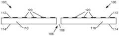
参照图1A、1B,示意性地示出了示例性显示器拼接块100。更具体地,图1A示意性地示出了显示器拼接块100的示例的前平面图,并且图1B示意性地示出了显示器拼接块100的示例的后平面图。显示器拼接块100包括基板110、一个或多个光源120、以及驱动电路或控制电子器件130。Referring to Figures 1A, 1B, anexemplary display tile 100 is schematically shown. More specifically, FIG. 1A schematically illustrates a front plan view of an example ofdisplay tile 100 , and FIG. 1B schematically illustrates a rear plan view of an example ofdisplay tile 100 .Display tile 100 includessubstrate 110 , one ormore light sources 120 , and drive circuitry orcontrol electronics 130 .

在所示出的示例中,基板110具有第一表面112(图1A),及与第一表面112相对的第二表面114(图1B),其中光源120设置在第一表面112上,并且控制电子器件130设置在第二表面114上。在示例中,第一表面112代表显示器拼接块100的正面或第一侧面102,第二表面114代表显示器拼接块100的背面或第二侧面104。此配置用于顶部发射显示器拼接块。底部发射显示器拼接块的其他配置也是可能的,其中光源120设置在第二表面114上(具有控制电子器件130)。In the example shown, thesubstrate 110 has a first surface 112 ( FIG. 1A ), and a second surface 114 ( FIG. 1B ) opposite thefirst surface 112 , where thelight source 120 is disposed on thefirst surface 112 and controlsElectronic device 130 is disposed onsecond surface 114 . In an example, thefirst surface 112 represents the front orfirst side 102 of thedisplay tile 100 and thesecond surface 114 represents the back orsecond side 104 of thedisplay tile 100 . This configuration is used for top emission display tiles. Other configurations of bottom emitting display tiles are possible, wherein thelight source 120 is disposed on the second surface 114 (with control electronics 130).

基板110可以由玻璃、玻璃陶瓷、陶瓷、或聚合物材料、或包括这种材料的不同组合的以层状或混合物形式形成的复合材料。在示例中,基板110可以具有在0.005mm与2mm之间的厚度,更具体地,包括在0.01mm与1mm之间,在0.01mm与0.7mm之间,在0.05mm与0.6mm之间,在0.1mm与0.5mm之间的厚度,或者在0.2mm至0.4mm之间。在示例中,基板110可以是矩形的形状,如图1A与1B所示,或者可以是其他规则或不规则几何形状。Substrate 110 may be formed of glass, glass-ceramic, ceramic, or polymeric materials, or composite materials formed in layers or mixtures including various combinations of such materials. In an example, thesubstrate 110 may have a thickness of between 0.005mm and 2mm, more specifically, including between 0.01mm and 1mm, between 0.01mm and 0.7mm, between 0.05mm and 0.6mm, in Thickness between 0.1mm and 0.5mm, or between 0.2mm and 0.4mm. In an example, thesubstrate 110 may be rectangular in shape, as shown in FIGS. 1A and 1B , or may be other regular or irregular geometric shapes.

光源120可以例如配置成包括任意数量的行与列或其他图案的数组。每个光源120电耦合到驱动电路,例如驱动电路或控制电子器件130,以驱动或控制每个光源120的操作。控制电子器件130可以包括例如驱动IC、薄膜晶体管、微驱动器IC、和/或电性互连。尽管示出为设置在第二表面114上,但是在其他示例中,控制电子器件130(或其部件)可以设置在第一表面112上(具有光源120)。每个光源120可以包括例如发光二极管(LED)、微型LED、有机发光二极管(OLED)、或其他合适的光源或光调制器,例如镜子或光阀。Thelight sources 120 may, for example, be configured to include an array of any number of rows and columns or other patterns. Eachlight source 120 is electrically coupled to a driver circuit, such as driver circuit orcontrol electronics 130 , to drive or control the operation of eachlight source 120 .Control electronics 130 may include, for example, driver ICs, thin film transistors, micro-driver ICs, and/or electrical interconnects. Although shown as being disposed on thesecond surface 114, in other examples, the control electronics 130 (or components thereof) may be disposed on the first surface 112 (with the light sources 120). Eachlight source 120 may include, for example, light emitting diodes (LEDs), micro LEDs, organic light emitting diodes (OLEDs), or other suitable light sources or light modulators, such as mirrors or light valves.

图1C示意性地示出了相邻显示器拼接块100、100的示例的侧视图。更具体地,如在图1C的示例中所示出的,显示器拼接块100、100各自包括具有第一表面112及与第一表面112相对的第二表面114的基板110,其中光源120设置在第一表面112上并且控制电子器件130(图1B)设置在第二表面114上。在其他示例中,可以改变在其上提供光源120和/或控制电子器件130的表面。在所示出的示例中,显示器拼接块100、100被配置为彼此相邻,使得接缝106存在于显示器拼接块100、100之间。在示例中,在相邻显示器拼接块100、100之间的接缝106处可以具有间隙108。如此,在示例中,接缝106包括在相邻显示器拼接块100、100之间的间隙108。FIG. 1C schematically illustrates a side view of an example ofadjacent display tiles 100 , 100 . More specifically, as shown in the example of FIG. 1C,display tiles 100, 100 each include asubstrate 110 having afirst surface 112 and asecond surface 114 opposite thefirst surface 112, wherein thelight source 120 is disposed at On thefirst surface 112 and control electronics 130 ( FIG. 1B ) are disposed on thesecond surface 114 . In other examples, the surface on which thelight source 120 and/or thecontrol electronics 130 are provided may be varied. In the example shown, thedisplay tiles 100 , 100 are configured adjacent to each other such that aseam 106 exists between thedisplay tiles 100 , 100 . In an example, there may begaps 108 atseams 106 betweenadjacent display tiles 100 , 100 . As such, in the example,seam 106 includesgap 108 betweenadjacent display tiles 100 , 100 .

在示例中,基板110可以具有如图1C所示的具有正方形角的边缘。在其他示例中,基板110的边缘可以是圆形的、倒角的、或具有从正面和背面对称或不对称的一些其他横截面形状。在示例中,基板110可以是基本平坦的或具有曲率半径<3m、<1m、<0.5m,或<0.2m。在示例中,间隙108可具有宽度<500um、<200um、<100um、<50um,或<20um。在示例中,基板110与间隙108的厚度之比可以在1:1至50,000:1之间、在0.1:1至10,000:1之间、在0.1:1至1000:1之间、在1:1至100:1之间,或在1:1至10:1之间。在示例中,显示器拼接块100的像素间距(光源120之间的间距)与间隙108的比可以在1:1至50:1之间、在1:1至20:1之间,或在5:1至10:1之间。In an example, thesubstrate 110 may have edges with square corners as shown in FIG. 1C . In other examples, the edges of thesubstrate 110 may be rounded, chamfered, or have some other cross-sectional shape that is symmetrical or asymmetric from the front and back. In an example, thesubstrate 110 may be substantially flat or have a radius of curvature <3m, <1m, <0.5m, or <0.2m. In an example, thegap 108 may have a width <500um, <200um, <100um, <50um, or <20um. In an example, the ratio of the thickness ofsubstrate 110 togap 108 may be between 1:1 to 50,000:1, between 0.1:1 to 10,000:1, between 0.1:1 to 1000:1, between 1:1 Between 1 and 100:1, or between 1:1 and 10:1. In an example, the ratio of pixel pitch (spacing between light sources 120 ) togap 108 ofdisplay tile 100 may be between 1:1 and 50:1, between 1:1 and 20:1, or between 5 : between 1 and 10:1.

图2示意性地示出了没有光学模糊化接缝的相邻显示器拼接块200、200的示例的侧视图。更具体地,如在图2的示例中所示出的,作为显示器拼接块100的示例的每个显示器拼接块200、200,包括具有第一表面212及与第一表面212相对的第二表面214的基板210,其具有设置在第一表面212上的光源220,及设置在第二表面214上的控制电子器件,如控制电子器件130(图1B)。在其他示例中,光源220和/或控制电子器件可以设置在其他表面上。在所示出的示例中,显示器拼接块200、200被配置为彼此相邻,使得接缝206存在于显示器拼接块200、200之间。在示例中,在相邻显示器拼接块200、200之间的接缝206处可以具有间隙208。如此,在示例中,接缝206包括在相邻显示器拼接块200、200之间的间隙208。Figure 2 schematically illustrates a side view of an example ofadjacent display tiles 200, 200 without optically blurred seams. More specifically, as shown in the example of FIG. 2 , eachdisplay tile 200 , 200 , which is an example of thedisplay tile 100 , includes afirst surface 212 and a second surface opposite thefirst surface 212Substrate 210 of 214 havinglight source 220 disposed onfirst surface 212, and control electronics, such ascontrol electronics 130, disposed on second surface 214 (FIG. IB). In other examples, thelight sources 220 and/or control electronics may be disposed on other surfaces. In the example shown, thedisplay tiles 200 , 200 are configured adjacent to each other such that aseam 206 exists between thedisplay tiles 200 , 200 . In an example, there may begaps 208 atseams 206 betweenadjacent display tiles 200 , 200 . As such, in the example,seam 206 includes agap 208 betweenadjacent display tiles 200 , 200 .

如在图2的示例中示意性地示出的,在接缝206未光学模糊化的情况下,来自外部光源的光(例如环境光292)从接缝206(更具体地,包括从相邻显示器拼接块200、200之间的间隙208)反射。另外,来自内部光源的光(例如来自光源220的光222)从接缝206(更具体地,包括从相邻显示器拼接块200、200之间的间隙208)反射。来自接缝206(更具体地,包括来自相邻显示器拼接块200、200之间的间隙208)的光的反射,包括来自显示器拼接块200、200的边缘或边缘界面(例如,相对边缘)的光的反射。As shown schematically in the example of FIG. 2 , without theseam 206 being optically blurred, light from an external light source (eg, ambient light 292 ) travels from the seam 206 (more specifically, including from adjacent Gap 208) betweendisplay tiles 200, 200 reflects. Additionally, light from an internal light source (eg, light 222 from light source 220) is reflected from seam 206 (more specifically, including fromgap 208 betweenadjacent display tiles 200, 200). Reflection of light from seams 206 (more specifically, including fromgaps 208 betweenadjacent display tiles 200 , 200 ), including from edges or edge interfaces (eg, opposing edges) ofdisplay tiles 200 , 200 reflection of light.

藉由从接缝206(更具体地,包括来自相邻显示器拼接块200、200之间的间隙208)反射的光,从间隙208反射或散射的光量,会不同于从显示器拼接块200、200反射或散射的光量。如此,从接缝206(更具体地,包括来自相邻显示器拼接块200、200之间的间隙208)反射的光,可能会导致光学缺陷,例如对比度降低、产生亮点或暗点或线条、和/或图像失真。例如,从接缝206(更具体地,包括来自相邻显示器拼接块200、200之间的间隙208)反射的光,可能会产生杂散光,这可能导致图像质量下降,或显示器拼接块的观看体验下降。具体地,与显示器拼接块200、200相比,环境光或由光源220产生的光在接缝206处(包括从间隙208)会不同地反射或透射。如观看者可观察到,反射或透射光的此差异可能会在拼接显示器上产生光强度变化。With light reflected from seams 206 (more specifically, including fromgaps 208 betweenadjacent display tiles 200, 200), the amount of light reflected or scattered fromgaps 208 will be different than fromdisplay tiles 200, 200 The amount of light reflected or scattered. As such, light reflected from seams 206 (and more specifically, including fromgaps 208 betweenadjacent display tiles 200, 200) may cause optical defects such as reduced contrast, the creation of bright or dark spots or lines, and / or image distortion. For example, light reflected from seams 206 (and more specifically, including fromgaps 208 betweenadjacent display tiles 200, 200) may generate stray light, which may result in reduced image quality, or viewing of the display tiles Experience declines. In particular, ambient light or light generated bylight sources 220 may be reflected or transmitted differently atseams 206, including fromgaps 208, compared to displaytiles 200, 200. This difference in reflected or transmitted light may produce light intensity variations on the tiled display as observable to the viewer.

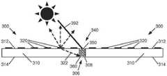
图3示意性地示出了具有光学模糊化接缝的相邻显示器拼接块300、300的示例的侧视图。更具体地,如在图3的示例中所示出的,每个作为显示器拼接块100的示例的显示器拼接块300、300,包括具有第一表面312及与第一表面312相对的第二表面314的基板310,其具有设置在第一表面312上的光源320,及设置在第二表面314上的控制电子器件,例如控制电子器件130(图1B)。在其他示例中,光源320和/或控制电子器件可以设置在其他表面上。在所示出的示例中,显示器拼接块300、300被配置为彼此相邻,使得接缝306存在于显示器拼接块300、300之间。在示例中,在相邻显示器拼接块300、300之间的接缝306处可以具有间隙308。如此,在示例中,接缝306包括在相邻显示器拼接块300、300之间的间隙308。Figure 3 schematically illustrates a side view of an example ofadjacent display tiles 300, 300 with optically blurred seams. More specifically, as shown in the example of FIG. 3 , eachdisplay tile 300 , 300 , which is an example ofdisplay tile 100 , includes afirst surface 312 and a second surface opposite thefirst surface 312Substrate 310 of 314 havinglight source 320 disposed onfirst surface 312, and control electronics, such as control electronics 130 (FIG. IB), disposed onsecond surface 314. In other examples, thelight sources 320 and/or control electronics may be disposed on other surfaces. In the example shown, thedisplay tiles 300 , 300 are configured adjacent to each other such that aseam 306 exists between thedisplay tiles 300 , 300 . In an example, there may begaps 308 atseams 306 betweenadjacent display tiles 300 , 300 . As such, in the example,seam 306 includes agap 308 betweenadjacent display tiles 300 , 300 .

在一个示例中,如图3所示,接缝306(更具体地,包括在相邻显示器拼接块300、300之间的间隙308)在接缝306(更具体地,包括在相邻显示器拼接块300、300之间的间隙308)处被光学元件340光学模糊化。光学元件340例如通过在接缝306处散射和/或吸收光来使相邻显示器拼接块300、300之间的接缝306光学模糊化。如此,在示例中,光学元件340光学地混合或分散来自接缝306和/或在接缝306处的光。另外,在示例中,光学元件340可以在相邻显示器拼接块300、300之间提供光学匹配。在所示出的示例中,光学元件340在相邻显示器拼接块300、300之间的间隙308内。In one example, as shown in FIG. 3, seam 306 (more specifically, includinggap 308 betweenadjacent display tiles 300, 300) at seam 306 (more specifically, including between adjacent display tiles) The gap 308) between theblocks 300, 300 is optically blurred by theoptical element 340.Optical element 340 optically blursseam 306 betweenadjacent display tiles 300 , 300 , eg, by scattering and/or absorbing light atseam 306 . As such, in an example,optical element 340 optically mixes or disperses light from and/or atseam 306 . Additionally, in an example, theoptical element 340 may provide optical matching betweenadjacent display tiles 300 , 300 . In the example shown, theoptical element 340 is within thegap 308 betweenadjacent display tiles 300 , 300 .

在示例中,光学元件340包括在接缝306处(更具体地,包括在相邻显示器拼接块300、300之间的间隙308内)的光学材料350。光学材料350可以包括例如,光学或光散射材料、光学或光吸收材料、和/或光学匹配材料。光学材料350的示例包括,光学散射材料,例如填充有纳米至微米尺寸的颗粒的光学黏合剂;或光学吸收材料,例如含有炭黑的材料;或光学匹配材料,例如折射率匹配光学黏合剂。在示例中,光学材料350可以在400nm至800nm的光学波长范围内具有基本均匀的光学响应(透射、散射、吸收)。在其他示例中,光学材料350可以在400nm至800nm的光学波长范围内具有变化的光学响应。In an example,optical element 340 includesoptical material 350 at seam 306 (more specifically, withingap 308 betweenadjacent display tiles 300, 300).Optical material 350 may include, for example, optical or light scattering materials, optical or light absorbing materials, and/or optical matching materials. Examples ofoptical material 350 include, optically scattering materials, such as optical adhesives filled with nanometer to micron sized particles; or optically absorbing materials, such as carbon black-containing materials; or optically matching materials, such as index matching optical adhesives. In an example, theoptical material 350 may have a substantially uniform optical response (transmission, scattering, absorption) in the optical wavelength range of 400 nm to 800 nm. In other examples, theoptical material 350 may have a varying optical response in the optical wavelength range of 400 nm to 800 nm.

在所示出的示例中,光学材料350基本上填充了相邻显示器拼接块300、300之间的间隙308。更具体地,在所示出的示例中,光学材料350接触并在相邻显示器拼接块300、300之间延伸,以便大致占据相邻显示器拼接块300、300之间的所有空间。In the example shown, theoptical material 350 substantially fills thegaps 308 betweenadjacent display tiles 300 , 300 . More specifically, in the example shown, theoptical material 350 contacts and extends betweenadjacent display tiles 300 , 300 so as to occupy substantially all of the space betweenadjacent display tiles 300 , 300 .

在示例中,光学元件340包括在接缝306处(更具体地,包括在相邻显示器拼接块300、300之间的间隙308内)的光学特征360。光学特征360可以包括例如光学或光散射特征和/或光学或光吸收特征。光学特征360的示例包括粗糙度、棱镜、双凸透镜、或其他物理结构。光学特征360可以被提供在,例如,光学元件340的表面或界面处或表面上或光学元件340内。In an example, theoptical element 340 includes anoptical feature 360 at the seam 306 (more specifically, within thegap 308 betweenadjacent display tiles 300, 300). Optical features 360 may include, for example, optical or light scattering features and/or optical or light absorbing features. Examples ofoptical features 360 include roughness, prisms, lenticular lenses, or other physical structures. Optical features 360 may be provided, for example, at or on a surface or interface ofoptical element 340 or withinoptical element 340 .

在所示出的示例中,光学特征360在接缝306处由光学材料350支撑。更具体地,在所示出的示例中,光学特征360由光学材料350支撑,如设置在相邻显示器拼接块300、300之间的间隙308内。In the example shown,optical feature 360 is supported byoptical material 350 atseam 306 . More specifically, in the example shown,optical features 360 are supported byoptical material 350 , such as disposed withingaps 308 betweenadjacent display tiles 300 , 300 .

如在图3的示例中示意性地示出的,随着包括光学材料350和/或光学特征360的光学元件340对接缝306的光学模糊化,来自外部光源的光(例如环境光392)在接缝306(更具体地,包括相邻显示器拼接块300、300之间的间隙308)处散射和/或吸收。此外,来自内部光源的光(例如来自光源320的光322)在接缝306(更具体地,包括相邻显示器拼接块300、300之间的间隙308)处散射和/或吸收。通过在接缝306(更具体地,包括相邻显示器拼接块300、300之间的间隙308)处散射和/或吸收光,可以减少或排除由接缝306(更具体地,包括相邻显示器拼接块300、300之间的间隙308)所引起的光学缺陷。具体地,与显示器拼接块300、300相比,环境光或从光源320产生的光,可以在接缝306处(包括从间隙308)类似地反射或透射。如此,在示例中,光学元件340可以在相邻显示器拼接块300、300之间提供光学匹配。As schematically shown in the example of FIG. 3 , light from an external light source (eg, ambient light 392 ) asoptical element 340 includingoptical material 350 and/oroptical feature 360 optically blursseam 306 . Scattering and/or absorption at seams 306 (more specifically, includinggaps 308 betweenadjacent display tiles 300, 300). Additionally, light from internal light sources (eg, light 322 from light source 320) is scattered and/or absorbed at seams 306 (more specifically, includinggaps 308 betweenadjacent display tiles 300, 300). By scattering and/or absorbing light at the seam 306 (more specifically, including thegaps 308 betweenadjacent display tiles 300, 300), the seams 306 (more specifically, including the adjacent displays) may be reduced or eliminated by scattering and/or absorbing light. Optical defects caused by gaps 308) betweentiles 300, 300. In particular, ambient light, or light generated fromlight source 320, may be similarly reflected or transmitted atseam 306, including fromgap 308, as compared to displaytiles 300, 300. As such, in an example, theoptical element 340 may provide optical matching betweenadjacent display tiles 300, 300.

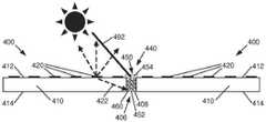
图4示意性地示出了具有光学模糊化接缝的相邻显示器拼接块400、400的示例的侧视图。更具体地,如在图4的示例中所示出的,作为显示器拼接块100的示例的每个显示器拼接块400、400,包括具有第一表面412及与第一表面412相对的第二表面414的基板410,其具有设置在第一表面412上的光源420,及设置在第二表面414上的控制电子器件,如控制电子器件130(图1B)。在其他示例中,光源420和/或控制电子器件可以设置在其他表面上。在所示出的示例中,显示器拼接块400、400被配置为彼此相邻,使得接缝406存在于显示器拼接块400、400之间。在示例中,在相邻显示器拼接块400、400之间的接缝406处可以具有间隙408。如此,在示例中,接缝406包括在相邻显示器拼接块400、400之间的间隙408。Figure 4 schematically illustrates a side view of an example ofadjacent display tiles 400, 400 with optically blurred seams. More specifically, as shown in the example of FIG. 4 , eachdisplay tile 400 , 400 , which is an example of thedisplay tile 100 , includes afirst surface 412 and a second surface opposite thefirst surface 412 .Substrate 410 of 414 havinglight source 420 disposed onfirst surface 412 and control electronics such ascontrol electronics 130 disposed on second surface 414 (FIG. IB). In other examples, thelight sources 420 and/or control electronics may be disposed on other surfaces. In the example shown, thedisplay tiles 400 , 400 are configured adjacent to each other such that aseam 406 exists between thedisplay tiles 400 , 400 . In an example, there may be agap 408 at theseam 406 betweenadjacent display tiles 400 , 400 . As such, in the example,seam 406 includes agap 408 betweenadjacent display tiles 400 , 400 .

在一个示例中,如图4所示,接缝406(更具体地,包括在相邻显示器拼接块400、400之间的间隙408)由在接缝406(更具体地,包括在相邻显示器拼接块400、400之间的间隙408)处的光学元件440光学模糊化。光学元件440例如通过在接缝406处散射和/或吸收光来使相邻显示器拼接块400、400之间的接缝406光学模糊化。如此,在示例中,光学元件440光学地混合或分散来自接缝406的和/或在接缝406处的光。另外,在示例中,光学元件440可以在相邻显示器拼接块400、400之间提供光学匹配。在所示出的示例中,光学元件440在相邻显示器拼接块400、400之间的间隙408之内和横跨其间。In one example, as shown in FIG. 4, seam 406 (more specifically, includinggap 408 betweenadjacent display tiles 400, 400) is formed by seam 406 (more specifically, including between adjacent displaysOptical element 440 at gap 408) betweentiles 400, 400 is optically blurred.Optical element 440 optically blursseam 406 betweenadjacent display tiles 400 , 400 , eg, by scattering and/or absorbing light atseam 406 . As such, in an example,optical element 440 optically mixes or disperses light from and/or atseam 406 . Additionally, in an example, theoptical element 440 may provide optical matching betweenadjacent display tiles 400 , 400 . In the example shown, theoptical element 440 is within and across thegap 408 betweenadjacent display tiles 400 , 400 .

在示例中,光学元件440包括在接缝406处(更具体地,包括在相邻显示器拼接块400、400之间的间隙408之内和横跨其间)的光学材料450。光学材料450可以包括例如,光学或光散射材料、光学或光吸收材料、和/或光学匹配材料。光学材料450的示例包括,光学散射材料,例如填充有纳米至微米尺寸的颗粒的光学黏合剂;或光学吸收材料,例如含有炭黑的材料;或光学匹配材料,例如折射率匹配光学黏合剂。在示例中,光学材料450可以在400nm至800nm的光学波长范围内具有基本均匀的光学响应(透射、散射、吸收)。在其他示例中,光学材料450可以在400nm至800nm的光学波长范围内具有变化的光学响应。In an example,optical element 440 includesoptical material 450 at seam 406 (more specifically, within and acrossgap 408 betweenadjacent display tiles 400, 400).Optical material 450 may include, for example, optical or light scattering materials, optical or light absorbing materials, and/or optical matching materials. Examples ofoptical material 450 include, optically scattering materials, such as optical adhesives filled with nanometer to micron sized particles; or optically absorbing materials, such as carbon black-containing materials; or optically matching materials, such as index matching optical adhesives. In an example, theoptical material 450 may have a substantially uniform optical response (transmission, scattering, absorption) in the optical wavelength range of 400 nm to 800 nm. In other examples, theoptical material 450 may have a varying optical response over the optical wavelength range of 400 nm to 800 nm.

在所示出的示例中,光学材料450包括基本上填充相邻显示器拼接块400、400之间的间隙408的光学材料452,以及延伸横跨相邻显示器拼接块400、400之间的间隙408(或在其上方)的光学材料454。光学材料452和光学材料454可以包括相同的材料或不同的材料。In the example shown,optical material 450 includesoptical material 452 that substantially fillsgap 408 betweenadjacent display tiles 400 , 400 and extends acrossgap 408 betweenadjacent display tiles 400 , 400 (or above) theoptical material 454.Optical material 452 andoptical material 454 may comprise the same material or different materials.

在示例中,光学元件440包括在接缝406(更具体地,包括在相邻显示器拼接块400、400之间的间隙408内)处的光学特征460。光学特征460可包括例如光学或光散射特征和/或光学或光吸收特征。光学特征460的示例包括粗糙度、棱镜、双凸透镜、或其他物理结构。可以在例如光学元件440的表面或界面处或表面上或在其内部提供光学特征460。In an example,optical element 440 includesoptical feature 460 at seam 406 (more specifically, withingap 408 betweenadjacent display tiles 400, 400). Optical features 460 may include, for example, optical or light scattering features and/or optical or light absorbing features. Examples ofoptical features 460 include roughness, prisms, lenticular lenses, or other physical structures. Optical features 460 may be provided, for example, at or on or within a surface or interface ofoptical element 440 .

在所示出的示例中,光学特征460在接缝406处由光学材料450支撑。更具体地,在所示出的示例中,光学特征460由如设置在相邻显示器拼接块400、400之间的间隙408内的光学材料452支撑。In the example shown,optical feature 460 is supported byoptical material 450 atseam 406 . More specifically, in the example shown,optical features 460 are supported byoptical material 452 as disposed withingaps 408 betweenadjacent display tiles 400 , 400 .

如在图4的示例中示意性地示出的,由于接缝406被包括光学材料450和/或光学特征460的光学元件440光学模糊化,来自外部光源的光,例如环境光492,在接缝406(更具体地,在相邻显示器拼接块400、400之间的间隙408)处被散射和/或散射。此外,来自内部光源的光(例如来自光源420的光422)在接缝406(更具体地,包括在相邻显示器拼接块400、400之间的间隙408)处散射和/或吸收。通过散射和/或吸收接缝406(更具体地,在相邻显示器拼接块400、400之间的间隙408)处的光,可以减少或排除由接缝406(更具体地,包括在相邻显示器拼接块400、400之间的间隙408)所引起的光学缺陷。具体地,与显示器拼接块400、400相比,环境光或从光源420产生的光,可以在接缝406(包括从间隙408)处被相似地反射或透射。如此,在示例中,光学元件440可以在相邻显示器拼接块400、400之间提供光学匹配。As shown schematically in the example of FIG. 4, sinceseam 406 is optically blurred byoptical element 440 includingoptical material 450 and/oroptical feature 460, light from an external light source, such asambient light 492, is The slits 406 (more specifically, thegaps 408 betweenadjacent display tiles 400, 400) are scattered and/or scattered. Additionally, light from internal light sources (eg, light 422 from light source 420) is scattered and/or absorbed at seams 406 (more specifically, includinggaps 408 betweenadjacent display tiles 400, 400). By scattering and/or absorbing light at the seam 406 (more specifically, in thegap 408 betweenadjacent display tiles 400, 400), the seams 406 (more specifically, including at theadjacent display tiles 400, 400) can be reduced or eliminated. Optical defects caused by gaps 408) betweendisplay tiles 400, 400. In particular, ambient light, or light generated fromlight source 420, may be similarly reflected or transmitted at seam 406 (including from gap 408) as compared to displaytiles 400, 400. As such, in an example, theoptical element 440 may provide optical matching betweenadjacent display tiles 400, 400.

图5示意性地示出了具有光学模糊化接缝的相邻显示器拼接块500、500的示例的侧视图。更具体地,如在图5的示例中所示出的,每个作为显示器拼接块100的示例的显示器拼接块500、500包括具有第一表面512及与第一表面512相对的第二表面514的基板510,其具有设置在第一表面512上的光源520,及设置在第二表面514上的控制电子器件,例如控制电子器件130(图1B)。在其他示例中,可以在其他表面上提供光源520和/或控制电子器件。在所示出的示例中,显示器拼接块500、500被配置为彼此相邻,使得接缝506存在于显示器拼接块500、500之间。在示例中,在相邻显示器拼接块500、500之间的接缝506处可以具有间隙508。如此,在示例中,接缝506包括在相邻显示器拼接块500、500之间的间隙508。Figure 5 schematically illustrates a side view of an example ofadjacent display tiles 500, 500 with optically blurred seams. More specifically, as shown in the example of FIG. 5 , eachdisplay tile 500 , 500 , which is an example ofdisplay tile 100 , includes afirst surface 512 and asecond surface 514 opposite thefirst surface 512 . Asubstrate 510 has alight source 520 disposed on afirst surface 512, and control electronics, such ascontrol electronics 130, disposed on a second surface 514 (FIG. 1B). In other examples,light sources 520 and/or control electronics may be provided on other surfaces. In the example shown, thedisplay tiles 500 , 500 are configured adjacent to each other such that aseam 506 exists between thedisplay tiles 500 , 500 . In an example, there may be agap 508 at theseam 506 betweenadjacent display tiles 500 , 500 . As such, in the example,seam 506 includes agap 508 betweenadjacent display tiles 500 , 500 .

在一个示例中,如图5所示,接缝506(更具体地,包括在相邻显示器拼接块500、500之间的间隙508)在接缝506(更具体地,包括在相邻显示器拼接块500、500之间的间隙508)处被光学元件540光学模糊化。光学元件540例如通过在接缝506处散射和/或吸收光来使相邻显示器拼接块500、500之间的接缝506光学模糊化。如此,在示例中,光学元件540光学地混合或分散来自接缝506和/或在接缝506处的光。另外,在示例中,光学元件540可以在相邻显示器拼接块500、500之间提供光学匹配。在所示出的示例中,光学元件540在相邻显示器拼接块500、500之间的间隙508之内和横跨其间。In one example, as shown in FIG. 5 , seam 506 (more specifically, includinggap 508 betweenadjacent display tiles 500 , 500 ) at seam 506 (more specifically, including between adjacent display tiles) The gap 508) between theblocks 500, 500 is optically blurred by theoptical element 540.Optical element 540 optically blursseam 506 betweenadjacent display tiles 500 , 500 , eg, by scattering and/or absorbing light atseam 506 . As such, in an example,optical element 540 optically mixes or disperses light from and/or atseam 506 . Additionally, in an example, theoptical element 540 may provide optical matching betweenadjacent display tiles 500 , 500 . In the example shown, theoptical element 540 is within and across thegap 508 betweenadjacent display tiles 500 , 500 .

在示例中,光学元件540包括在接缝506处(更具体地,包括在相邻显示器拼接块500、500之间的间隙508之内和横跨其间)的光学材料550。光学材料550可以包括例如光学或光散射材料、光学或光吸收材料、和/或光学匹配材料。光学材料550的示例包括,光学散射材料,例如填充有纳米至微米尺寸的颗粒的光学黏合剂;或光学吸收材料,例如含有炭黑的材料;或光学匹配材料,例如折射率匹配光学黏合剂。在示例中,光学材料550可以在400nm至800nm的光学波长范围内具有基本均匀的光学响应(透射、散射、吸收)。在其他示例中,光学材料550可以在400nm至800nm的光学波长范围内具有变化的光学响应。In an example,optical element 540 includesoptical material 550 at seam 506 (more specifically, within and acrossgap 508 betweenadjacent display tiles 500, 500).Optical material 550 may include, for example, optical or light scattering materials, optical or light absorbing materials, and/or optical matching materials. Examples ofoptical material 550 include, optically scattering materials, such as optical binders filled with nanometer to micron sized particles; or optically absorbing materials, such as carbon black-containing materials; or optically matching materials, such as index matching optical binders. In an example, theoptical material 550 may have a substantially uniform optical response (transmission, scattering, absorption) in the optical wavelength range of 400 nm to 800 nm. In other examples, theoptical material 550 may have a varying optical response in the optical wavelength range of 400 nm to 800 nm.

在所示出的示例中,光学材料550包括基本上填充相邻显示器拼接块500、500之间的间隙508的光学材料552,及延伸横跨相邻显示器拼接块500、500之间的间隙508(或在其上方)的光学材料554。光学材料552和光学材料554可以包括相同的材料或不同的材料。在示例中,光学材料554包括覆盖玻璃或聚合物材料层,其在相邻显示器拼接块500、500的光源520上延伸,使得光学材料554接触相邻显示器拼接块500、500的第一表面512。覆盖玻璃的例子包括离子交换玻璃、化学强化玻璃,例如康宁公司(Corning Incorporated)生产的

Figure BDA0003639104430000111
玻璃、碱石灰玻璃、拉制或轧制或浮法玻璃板、或无碱玻璃。In the example shown, theoptical material 550 includes anoptical material 552 that substantially fills thegap 508 betweenadjacent display tiles 500 , 500 and extends across thegap 508 betweenadjacent display tiles 500 , 500 (or above) theoptical material 554.Optical material 552 andoptical material 554 may comprise the same material or different materials. In an example, theoptical material 554 includes a cover glass or a layer of polymer material that extends over thelight sources 520 ofadjacent display tiles 500 , 500 such that theoptical material 554 contacts thefirst surface 512 of theadjacent display tiles 500 , 500 . Examples of cover glass include ion-exchanged glass, chemically strengthened glass such as those produced by Corning Incorporated
Figure BDA0003639104430000111
Glass, soda-lime glass, drawn or rolled or float glass sheets, or soda-free glass.

在示例中,光学元件540在接缝506处(更具体地,包括在相邻显示器拼接块500、500之间的间隙508内,以及横跨相邻显示器拼接块500、500之间的间隙508)包括光学特征560。光学特征560可包括例如光学或光散射特征和/或光学或光吸收特征。光学特征560的示例包括粗糙度、棱镜、双凸透镜、或其他物理结构。可以在例如光学元件540的表面或界面处或表面上或在其内部提供光学特征560。In the example,optical element 540 is at seam 506 (more specifically, included withingap 508 betweenadjacent display tiles 500 , 500 and acrossgap 508 betweenadjacent display tiles 500 , 500 ) ) includesoptical feature 560. Optical features 560 may include, for example, optical or light scattering features and/or optical or light absorbing features. Examples ofoptical features 560 include roughness, prisms, lenticular lenses, or other physical structures. Optical features 560 may be provided, for example, at or on or within a surface or interface ofoptical element 540 .

在所示出的示例中,光学特征560在接缝506处由光学材料550支撑。更具体地,在所示出的示例中,光学特征560包括由如设置在相邻显示器拼接块500、500之间的间隙508内的光学材料552支撑的光学特征562,以及由如设置于横跨相邻显示器拼接块500、500之间的间隙508(或在其上方)的光学材料554支撑的光学特征564。如此,光学特征562提供在相邻显示器拼接块500、500之间的间隙508内,并且光学特征564提供于横跨(或在于)相邻显示器拼接块500、500之间的间隙508。光学特征562与光学特征564可以包括相同或不同的特征。In the example shown,optical feature 560 is supported byoptical material 550 atseam 506 . More specifically, in the example shown, theoptical features 560 includeoptical features 562 supported byoptical material 552 such as disposed withingaps 508 betweenadjacent display tiles 500, 500, andoptical features 562 such as disposed in a transverse direction. Optical features 564 supported byoptical material 554 acrossgaps 508 betweenadjacent display tiles 500, 500 (or above). As such,optical features 562 are provided withingaps 508 betweenadjacent display tiles 500 , 500 andoptical features 564 are provided across (or within)gaps 508 betweenadjacent display tiles 500 , 500 .Optical feature 562 andoptical feature 564 may comprise the same or different features.

如在图5的示例中示意性地示出的,随着包括光学材料550和/或光学特征560的光学元件540对接缝506的光学模糊化,来自外部光源的光(例如环境光592)在接缝506处(更具体地,包括在相邻显示器拼接块500、500之间的间隙508处)被散射和/或吸收。此外,来自内部光源的光(例如来自光源520的光522)在接缝506(更具体地,包括在相邻显示器拼接块500、500之间的间隙508)处散射和/或吸收。通过在接缝506(更具体地,包括在相邻显示器拼接块500、500之间的间隙508)处散射和/或吸收光,可以减少或排除由接缝506(更具体地,包括在相邻显示器拼接块500、500之间的间隙508)所引起的光学缺陷。具体地,与显示器拼接块500、500相比,环境光或从光源520产生的光,可以在接缝506(包括从间隙508)处被相似地反射或透射。如此,在示例中,光学元件540可以在相邻显示器拼接块500、500之间提供光学匹配。As schematically shown in the example of FIG. 5 , light from an external light source (eg, ambient light 592 ) optically blursseam 506 byoptical element 540 includingoptical material 550 and/oroptical feature 560 . Scattered and/or absorbed at seams 506 (more specifically, including atgaps 508 betweenadjacent display tiles 500, 500). Additionally, light from internal light sources (eg, light 522 from light source 520) is scattered and/or absorbed at seams 506 (more specifically, includinggaps 508 betweenadjacent display tiles 500, 500). By scattering and/or absorbing light at the seam 506 (more specifically, including thegap 508 betweenadjacent display tiles 500, 500), it may be reduced or eliminated from the seam 506 (more specifically, including at the phase Optical defects caused by gaps 508) betweenadjacent display tiles 500, 500. In particular, ambient light, or light generated fromlight source 520, may be similarly reflected or transmitted at seam 506 (including from gap 508) as compared to displaytiles 500, 500. As such, in an example,optical element 540 may provide optical matching betweenadjacent display tiles 500, 500.

图6示意性地示出了具有光学模糊化接缝的相邻显示器拼接块600、600的示例的侧视图。更具体地,如在图6的示例中所示出的,作为显示器拼接块100的示例的每个显示器拼接块600、600,包括具有第一表面612及与第一表面612相对的第二表面614的基板610,其具有设置在第一表面612上的光源620,及设置在第二表面614上的控制电子器件,如控制电子器件130(图1B)。在其他示例中,光源620和/或控制电子器件可以设置在其他表面上。在所示出的示例中,显示器拼接块600、600被配置为彼此相邻,使得接缝606存在于显示器拼接块600、600之间。在示例中,在相邻显示器拼接块600、600之间的接缝606处可以具有间隙608。如此,在示例中,接缝606包括在相邻显示器拼接块600、600之间的间隙608。Figure 6 schematically illustrates a side view of an example ofadjacent display tiles 600, 600 with optically blurred seams. More specifically, as shown in the example of FIG. 6 , eachdisplay tile 600 , 600 , which is an example ofdisplay tile 100 , includes afirst surface 612 and a second surface opposite thefirst surface 612 .Substrate 610 of 614 havinglight source 620 disposed onfirst surface 612 and control electronics such ascontrol electronics 130 disposed on second surface 614 (FIG. IB). In other examples, thelight sources 620 and/or control electronics may be disposed on other surfaces. In the example shown, thedisplay tiles 600 , 600 are configured adjacent to each other such that aseam 606 exists between thedisplay tiles 600 , 600 . In an example, there may begaps 608 atseams 606 betweenadjacent display tiles 600 , 600 . As such, in the example,seam 606 includes agap 608 betweenadjacent display tiles 600 , 600 .

在一个示例中,如图6中所示,接缝606(更具体地,包括在在相邻显示器拼接块600、600之间的间隙608),在接缝606(更具体地,包括在在相邻显示器拼接块600、600之间的间隙608)处被光学元件640光学模糊化。光学元件640例如通过在接缝606处散射和/或吸收光来使相邻显示器拼接块600、600之间的接缝606光学模糊化。如此,在示例中,光学元件640光学地混合或分散来自接缝606和/或在接缝606处的光。另外,在示例中,光学元件640可以在相邻显示器拼接块600、600之间提供光学匹配。在所示出的示例中,光学元件640横跨相邻显示器拼接块600、600之间的间隙608。In one example, as shown in FIG. 6, seam 606 (more specifically, includinggap 608 betweenadjacent display tiles 600, 600), at seam 606 (more specifically, including at Thegaps 608 betweenadjacent display tiles 600, 600 are optically blurred byoptical elements 640.Optical element 640 optically blursseam 606 betweenadjacent display tiles 600 , 600 , eg, by scattering and/or absorbing light atseam 606 . As such, in an example,optical element 640 optically mixes or disperses light from and/or atseam 606 . Additionally, in an example, theoptical element 640 may provide optical matching betweenadjacent display tiles 600 , 600 . In the example shown, theoptical element 640 spans thegap 608 betweenadjacent display tiles 600 , 600 .

在示例中,光学元件640在接缝606(更具体地,包括在相邻显示器拼接块600、600之间的间隙608)处包括光学材料650。光学材料650可以包括例如,光学或光散射材料、光学或光吸收材料、和/或光学匹配材料。光学材料650的示例包括,光学散射材料,例如填充有纳米至微米尺寸的颗粒的光学黏合剂;或光学吸收材料,例如含有炭黑的材料;或光学匹配材料,例如折射率匹配光学黏合剂。在示例中,光学材料650可以在400nm至800nm的光学波长范围内具有基本均匀的光学响应(透射、散射、吸收)。在其他示例中,光学材料650可以在400nm至800nm的光学波长范围内具有变化的光学响应。In an example,optical element 640 includesoptical material 650 at seam 606 (more specifically, includinggap 608 betweenadjacent display tiles 600, 600).Optical material 650 may include, for example, optical or light scattering materials, optical or light absorbing materials, and/or optical matching materials. Examples ofoptical materials 650 include optical scattering materials, such as optical binders filled with nanometer to micron sized particles; or optically absorbing materials, such as carbon black-containing materials; or optical matching materials, such as index matching optical binders. In an example, theoptical material 650 may have a substantially uniform optical response (transmission, scattering, absorption) in the optical wavelength range of 400 nm to 800 nm. In other examples, theoptical material 650 may have a varying optical response over the optical wavelength range of 400 nm to 800 nm.

在所示出的示例中,光学材料650延伸横跨相邻显示器拼接块600、600之间的间隙608(或在其上方)。在示例中,光学材料650包括覆盖玻璃或聚合物材料层,该覆盖玻璃或聚合物材料层在相邻显示器拼接块600、600的光源620上延伸,使得光学材料650与相邻显示器拼接块600、600的第一表面612间隔开。覆盖玻璃的例子包括离子交换玻璃、化学强化玻璃,例如康宁公司(Corning Incorporated)生产的

Figure BDA0003639104430000131
玻璃、碱石灰玻璃、拉制或轧制或浮法玻璃板、或无碱玻璃。In the example shown, theoptical material 650 extends across (or over) thegap 608 betweenadjacent display tiles 600 , 600 . In an example, theoptical material 650 includes a layer of cover glass or polymer material that extends over thelight sources 620 ofadjacent display tiles 600 , 600 such that theoptical material 650 is aligned with theadjacent display tiles 600 Thefirst surfaces 612 of , 600 are spaced apart. Examples of cover glass include ion-exchanged glass, chemically strengthened glass such as those produced by Corning Incorporated
Figure BDA0003639104430000131
Glass, soda-lime glass, drawn or rolled or float glass sheets, or soda-free glass.

在示例中,光学元件640包括在接缝606处(更具体地,包括在相邻显示器拼接块600、600之间的间隙608)的光学特征660。光学特征660可包括例如光学或光散射特征和/或光学或光吸收特征。光学特征660的示例包括粗糙度、棱镜、双凸透镜、或其他物理结构。可以在例如光学元件640的表面或界面处或表面上或在其内部提供光学特征660。In an example,optical element 640 includesoptical feature 660 at seam 606 (more specifically, includinggap 608 betweenadjacent display tiles 600, 600). Optical features 660 may include, for example, optical or light scattering features and/or optical or light absorbing features. Examples ofoptical features 660 include roughness, prisms, lenticular lenses, or other physical structures. Optical features 660 may be provided, for example, at or on or within a surface or interface ofoptical element 640 .

在所示出的示例中,光学特征660在接缝606处由光学材料650支撑。更具体地,在所示出的示例中,光学特征660由如设置于横跨相邻显示器拼接块600、600之间的间隙608(或在其上方)的光学材料650支撑。如此,光学特征660提供于横跨(或在于)相邻显示器拼接块600、600之间的间隙608。In the example shown,optical feature 660 is supported byoptical material 650 atseam 606 . More specifically, in the example shown,optical features 660 are supported byoptical material 650 as disposed across (or over)gap 608 betweenadjacent display tiles 600 , 600 . As such,optical features 660 are provided across (or within) thegap 608 betweenadjacent display tiles 600 , 600 .

如在图6的示例中示意性地示出的那样,由于接缝606被包括光学材料650和/或光学特征660的光学元件640光学模糊化,来自外部光源的光(例如环境光692)在接缝606处(更具体地,包括在相邻显示器拼接块600、600之间的间隙608处)散射和/或吸收。此外,来自内部光源的光(例如来自光源620的光622)在接缝606处(更具体地,包括在相邻显示器拼接块600、600之间的间隙608处)散射和/或吸收。通过在接缝606处(更具体地,包括在相邻显示器拼接块600、600之间的间隙608处)散射和/或吸收光,可以减少或排除由接缝606(更具体地,包括在相邻显示器拼接块600、600之间的间隙608)导致的光学缺陷。具体地,与显示器拼接块600、600相比,环境光或从光源620产生的光,可以在接缝606处(包括从间隙608)类似地反射或透射。如此,在示例中,光学元件640可以在相邻显示器拼接块600、600之间提供光学匹配。As shown schematically in the example of FIG. 6, sinceseam 606 is optically blurred byoptical element 640 includingoptical material 650 and/oroptical feature 660, light from an external light source (eg, ambient light 692) is Scattering and/or absorption at seams 606 (more specifically, including atgaps 608 betweenadjacent display tiles 600, 600). Additionally, light from internal light sources (eg, light 622 from light source 620) is scattered and/or absorbed at seams 606 (more specifically, including atgaps 608 betweenadjacent display tiles 600, 600). By scattering and/or absorbing light at the seam 606 (more specifically, including at thegap 608 betweenadjacent display tiles 600, 600), reduction or elimination of the Optical defects caused bygaps 608 betweenadjacent display tiles 600, 600). In particular, ambient light, or light generated fromlight source 620, may be similarly reflected or transmitted atseam 606, including fromgap 608, as compared to displaytiles 600, 600. As such, in an example, theoptical element 640 may provide an optical match betweenadjacent display tiles 600, 600.

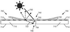
图7示意性地示出了具有光学模糊化接缝的相邻显示器拼接块700、700的示例的侧视图。更具体地,如在图7的示例中所示出的,每个作为显示器拼接块100的示例的显示器拼接块700、700,包括具有第一表面712及与第一表面712相对的第二表面714的基板710,其具有设置在第一表面712上的光源720,及设置在第二表面714上的控制电子器件,例如控制电子器件130(图1B)。在其他示例中,光源720和/或控制电子器件可以设置在其他表面上。在所示出的示例中,显示器拼接块700、700被配置为彼此相邻,使得接缝706存在于显示区块700、700之间。在示例中,在相邻显示器拼接块700、700之间的接缝706处可以具有间隙708。如此,在示例中,接缝706包括在相邻显示器拼接块700、700之间的间隙708。Figure 7 schematically illustrates a side view of an example ofadjacent display tiles 700, 700 with optically blurred seams. More specifically, as shown in the example of FIG. 7 , eachdisplay tile 700 , 700 , which is an example ofdisplay tile 100 , includes afirst surface 712 and a second surface opposite thefirst surface 712Substrate 710 of 714 havinglight source 720 disposed onfirst surface 712, and control electronics, such as control electronics 130 (FIG. IB), disposed onsecond surface 714. In other examples, thelight sources 720 and/or control electronics may be disposed on other surfaces. In the example shown, thedisplay tiles 700 , 700 are configured adjacent to each other such that aseam 706 exists between thedisplay tiles 700 , 700 . In an example, there may be agap 708 at theseam 706 betweenadjacent display tiles 700 , 700 . As such, in the example,seam 706 includes agap 708 betweenadjacent display tiles 700 , 700 .

在一个示例中,如图7所示,接缝706(更具体地,包括在相邻显示器拼接块700、700之间的间隙708)在接缝706处(更具体地,包括在相邻显示器拼接块700、700之间的间隙708处)被光学元件740光学模糊化。光学元件740例如通过在接缝706处散射和/或吸收光,来使相邻显示器拼接块700、700之间的接缝706光学模糊化。如此,在示例中,光学元件740光学地混合或分散来自接缝706和/或在接缝706处的光。另外,在示例中,光学元件740可以在相邻显示器拼接块700、700之间提供光学匹配。在所示出的示例中,光学元件740横跨相邻显示器拼接块700、700之间的间隙708。In one example, as shown in FIG. 7, seam 706 (more specifically, includinggap 708 betweenadjacent display tiles 700, 700) is at seam 706 (more specifically, including between adjacent displays The gap 708) between thetiles 700, 700 is optically blurred by theoptical element 740.Optical element 740 optically blursseam 706 betweenadjacent display tiles 700 , 700 , eg, by scattering and/or absorbing light atseam 706 . As such, in an example,optical element 740 optically mixes or disperses light from and/or atseam 706 . Additionally, in an example, theoptical element 740 may provide optical matching betweenadjacent display tiles 700 , 700 . In the example shown, theoptical element 740 spans thegap 708 betweenadjacent display tiles 700 , 700 .

在示例中,光学元件740包括在接缝706(更具体地,包括相邻显示器拼接块700、700之间的间隙708)处的光学材料750。光学材料750可以包括例如,光学或光散射材料、光学或光吸收材料、和/或光学匹配材料。光学材料750的示例包括,光学散射材料,例如填充有纳米至微米尺寸的颗粒的光学黏合剂;或光学吸收材料,例如含有炭黑的材料;或光学匹配材料,例如折射率匹配光学黏合剂。在示例中,光学材料750可以在400nm至800nm的光学波长范围内具有基本均匀的光学响应(透射、散射、吸收)。在其他示例中,光学材料750可以在400nm至800nm的光学波长范围内具有变化的光学响应。In an example,optical element 740 includesoptical material 750 at seam 706 (more specifically, includinggap 708 betweenadjacent display tiles 700, 700).Optical material 750 may include, for example, optical or light scattering materials, optical or light absorbing materials, and/or optical matching materials. Examples ofoptical materials 750 include optical scattering materials, such as optical binders filled with nanometer to micron sized particles; or optically absorbing materials, such as carbon black-containing materials; or optical matching materials, such as index matching optical binders. In an example, theoptical material 750 may have a substantially uniform optical response (transmission, scattering, absorption) in the optical wavelength range of 400 nm to 800 nm. In other examples, theoptical material 750 may have a varying optical response in the optical wavelength range of 400 nm to 800 nm.

在所示出的示例中,光学材料750延伸横跨相邻显示器拼接块700、700之间的间隙708(或在其上方)。在示例中,光学材料750包括覆盖玻璃或聚合物材料层,该覆盖玻璃或聚合物材料层在相邻显示器拼接块700、700的光源720上延伸,使得光学材料750接触相邻显示器拼接块700、700的第一表面712。覆盖玻璃的例子包括离子交换玻璃、化学强化玻璃,例如康宁公司(Corning Incorporated)生产的

Figure BDA0003639104430000141
玻璃、碱石灰玻璃、拉制或轧制或浮法玻璃板、或无碱玻璃。In the example shown, theoptical material 750 extends across (or over) thegap 708 betweenadjacent display tiles 700 , 700 . In an example, theoptical material 750 includes a layer of cover glass or polymer material that extends over thelight sources 720 ofadjacent display tiles 700 , 700 such that theoptical material 750 contacts theadjacent display tile 700 , thefirst surface 712 of 700 . Examples of cover glass include ion-exchanged glass, chemically strengthened glass such as those produced by Corning Incorporated
Figure BDA0003639104430000141
Glass, soda-lime glass, drawn or rolled or float glass sheets, or soda-free glass.

如在图7的示例中示意性地示出的,随着包括光学材料750的光学元件740对接缝706的光学模糊化,来自外部光源的光(例如环境光792)在接缝706处(更具体地,包括在相邻显示器拼接块700、700之间的间隙708处)被散射和/或吸收。另外,来自内部光源的光,例如来自光源720的光722,在接缝706处(更具体地,包括在相邻显示器拼接块700、700之间的间隙708处)被散射和/或吸收。通过在接缝706处(更具体地,包括在相邻显示器拼接块700、700之间的间隙708处)散射和/或吸收光,可以减小或消除由接缝706(更具体地,包括在相邻显示器拼接块700、700之间的间隙708)所引起的光学缺陷。具体地,与显示器拼接块700、700相比,环境光或从光源720产生的光可以相似地在接缝706处被反射或透射,包括从间隙708反射或透射。如此,在示例中,光学元件740可以在相邻显示器拼接块700、700之间提供光学匹配。As shown schematically in the example of FIG. 7 , as theoptical element 740 including theoptical material 750 optically blurs theseam 706 , light from an external light source (eg, ambient light 792 ) appears at the seam 706 ( More specifically, including atgaps 708 betweenadjacent display tiles 700, 700) are scattered and/or absorbed. Additionally, light from internal light sources, such as light 722 fromlight source 720, is scattered and/or absorbed at seams 706 (more specifically, including atgaps 708 betweenadjacent display tiles 700, 700). By scattering and/or absorbing light at the seam 706 (more specifically, including at thegap 708 betweenadjacent display tiles 700, 700), the loss of light from the seam 706 (more specifically, including Optical defects caused by gaps 708) betweenadjacent display tiles 700, 700. In particular, ambient light or light generated fromlight source 720 may be similarly reflected or transmitted atseam 706 , including fromgap 708 , compared to displaytiles 700 , 700 . As such, in an example, theoptical element 740 may provide an optical match betweenadjacent display tiles 700, 700.

图8示意性地示出了具有光学模糊化接缝的相邻显示器拼接块800、800的示例的侧视图。更具体地,如在图8的示例中所示出的,每一个作为显示器拼接块100的示例的显示器拼接块800、800,包括基板810,其具有第一表面812及与第一表面812相对的第二表面814,其中光源820设置在第一表面812上,且控制电子器件如控制电子器件130(图1B)设置在第二表面814上。在其他示例中,可以在其他表面上提供光源820和/或控制电子器件。在所示出的示例中,显示器拼接块800、800被配置为彼此相邻,使得接缝806存在于显示器拼接块800、800之间。在示例中,在相邻显示器拼接块800、800之间的接缝806处可以具有间隙808。如此,在示例中,接缝806包括在相邻显示器拼接块800、800之间的间隙808。Figure 8 schematically illustrates a side view of an example ofadjacent display tiles 800, 800 with optically blurred seams. More specifically, as shown in the example of FIG. 8 , eachdisplay tile 800 , 800 , which is an example ofdisplay tile 100 , includes asubstrate 810 having afirst surface 812 and opposing thefirst surface 812 Thesecond surface 814, wherein thelight source 820 is disposed on thefirst surface 812, and the control electronics such as the control electronics 130 (FIG. 1B) are disposed on thesecond surface 814. In other examples,light sources 820 and/or control electronics may be provided on other surfaces. In the example shown, thedisplay tiles 800 , 800 are configured adjacent to each other such that aseam 806 exists between thedisplay tiles 800 , 800 . In an example, there may be agap 808 at theseam 806 betweenadjacent display tiles 800 , 800 . As such, in the example,seam 806 includes agap 808 betweenadjacent display tiles 800 , 800 .

在一个示例中,如图8所示,接缝806(更具体地,包括相邻显示器拼接块800、800之间的间隙808),在接缝806处(更具体地,包括相邻显示器拼接块800、800之间的间隙808处)由光学元件840光学模糊化。光学元件840例如通过在接缝806处散射和/或吸收光,来使相邻显示器拼接块800、800之间的接缝806光学模糊化。如此,在示例中,光学元件840光学地混合或分散来自接缝806和/或在接缝806处的光。另外,在示例中,光学元件840可以在相邻显示器拼接块800、800之间提供光学匹配。在所示出的示例中,光学元件840横跨相邻显示器拼接块800、800之间的间隙808。In one example, as shown in FIG. 8, seam 806 (more specifically, includinggap 808 betweenadjacent display tiles 800, 800), at seam 806 (more specifically, including adjacent display tiles Thegap 808 betweenblocks 800 , 800 is optically blurred byoptical element 840 .Optical element 840 optically blursseam 806 betweenadjacent display tiles 800 , 800 , eg, by scattering and/or absorbing light atseam 806 . As such, in an example,optical element 840 optically mixes or disperses light from and/or atseam 806 . Additionally, in an example, theoptical element 840 may provide optical matching betweenadjacent display tiles 800, 800. In the example shown, theoptical element 840 spans thegap 808 betweenadjacent display tiles 800 , 800 .

在示例中,光学元件840包括在接缝806处(更具体地,包括横跨相邻显示器拼接块800、800之间的间隙808)的光学材料850。光学材料850可以包括例如,光学或光散射材料、光学或光吸收材料、和/或光学匹配材料。光学材料850的示例包括,光学散射材料,例如填充有纳米至微米尺寸的颗粒的光学黏合剂;或光学吸收材料,例如含有炭黑的材料;或光学匹配材料,例如折射率匹配光学黏合剂。在示例中,光学材料850可以在400nm至800nm的光学波长范围内具有基本均匀的光学响应(透射、散射、吸收)。在其他示例中,光学材料850可以在400nm至800nm的光学波长范围内具有变化的光学响应。In an example,optical element 840 includesoptical material 850 at seam 806 (more specifically, includinggap 808 spanning betweenadjacent display tiles 800, 800).Optical material 850 may include, for example, optical or light scattering materials, optical or light absorbing materials, and/or optical matching materials. Examples ofoptical materials 850 include optical scattering materials, such as optical binders filled with nanometer to micron sized particles; or optically absorbing materials, such as carbon black-containing materials; or optical matching materials, such as index matching optical binders. In an example, theoptical material 850 may have a substantially uniform optical response (transmission, scattering, absorption) in the optical wavelength range of 400 nm to 800 nm. In other examples, theoptical material 850 may have a varying optical response in the optical wavelength range of 400 nm to 800 nm.

在所示出的示例中,光学材料850延伸横跨相邻显示器拼接块800、800之间的间隙808(或在其上方)。在示例中,光学材料850包括覆盖玻璃或聚合物材料层,其在相邻显示器拼接块800、800的光源820上延伸,使得光学材料850接触相邻显示器拼接块800、800的第一表面812。覆盖玻璃的例子包括离子交换玻璃、化学强化玻璃,例如康宁公司(CorningIncorporated)生产的

Figure BDA0003639104430000161
玻璃、碱石灰玻璃、拉制或轧制或浮法玻璃板、或无碱玻璃。In the example shown, theoptical material 850 extends across (or above) thegap 808 betweenadjacent display tiles 800, 800. In an example, theoptical material 850 includes a layer of cover glass or polymer material that extends over thelight sources 820 ofadjacent display tiles 800 , 800 such that theoptical material 850 contacts thefirst surfaces 812 of theadjacent display tiles 800 , 800 . Examples of cover glass include ion-exchanged glass, chemically strengthened glass such as those produced by Corning Incorporated
Figure BDA0003639104430000161
Glass, soda-lime glass, drawn or rolled or float glass sheets, or soda-free glass.

在示例中,光学元件840包括在接缝806(更具体地,包括横跨相邻显示器拼接块800、800之间的间隙808)处的光学特征860。光学特征860可以包括例如光学或光散射特征和/或光学或光吸收特征。光学特征860的示例包括粗糙度、棱镜、双凸透镜、或其他物理结构。可以在例如光学元件840的表面或界面处或表面上或在其主体内提供光学特征860。In an example,optical element 840 includesoptical feature 860 at seam 806 (more specifically, includinggap 808 spanning betweenadjacent display tiles 800, 800). Optical features 860 may include, for example, optical or light scattering features and/or optical or light absorbing features. Examples ofoptical features 860 include roughness, prisms, lenticular lenses, or other physical structures. Optical features 860 may be provided, for example, at or on a surface or interface ofoptical element 840 or within the body thereof.

在所示出的示例中,光学特征860在接缝806处由光学材料850支撑。更具体地,在所示出的示例中,光学特征860由如设置于横跨相邻显示器拼接块800、800之间的间隙808(或在其上方)的光学材料850支撑。如此,光学特征860提供于横跨(或在于)相邻显示器拼接块800、800之间的间隙808。在示例中,光学特征860包括在光学材料850的侧上由光学材料850支撑的光学特征862,以及在光学材料850的相反侧上由光学材料850支撑的光学特征864。光学特征862与光学特征864可以包括相同或不同的特征。在示例中,光学特征862包括镜面反射器(或反射器),从而反射光离开光滑表面,使得入射光在反射时保持集中,并且光学特征864包括漫反射器(或反射器),从而反射光离开粗糙表面,使得入射光在反射时会分散在多个方向上。如此,在示例中,光学特征862将光反射到光学特征864,从而光学特征864散射经反射的光。In the example shown,optical feature 860 is supported byoptical material 850 atseam 806 . More specifically, in the example shown,optical feature 860 is supported byoptical material 850 as disposed across (or over)gap 808 betweenadjacent display tiles 800, 800. As such,optical features 860 are provided across (or within) thegap 808 between adjacent display tiles 800,800. In an example,optical features 860 includeoptical features 862 supported byoptical material 850 on one side ofoptical material 850 , andoptical features 864 supported byoptical material 850 on an opposite side ofoptical material 850 . Optical features 862 and 864 may comprise the same or different features. In an example, theoptical feature 862 includes a specular reflector (or reflector) to reflect light off a smooth surface such that incident light remains concentrated upon reflection, and theoptical feature 864 includes a diffuse reflector (or reflector) to reflect the light Leaves rough surfaces so that incident light is scattered in multiple directions when reflected. As such, in the example,optical features 862 reflect light tooptical features 864 such thatoptical features 864 scatter the reflected light.

如在图8的示例中示意性地所示出的,由于接缝806被包括光学材料850和/或光学特征860的光学元件840的光学模糊化,来自内部光源的光,如来自光源820的光822,在接缝806处(更具体地,包括在相邻显示器拼接块800、800之间的间隙808处)被散射和/或吸收。通过散射和/或吸收在接缝806(更具体地,包括相邻显示器拼接块800、800之间的间隙808)处的光,可以减少或排除由接缝806(更具体地,包括相邻显示器拼接块800、800之间的间隙808)所引起的光学缺陷。特别地,与显示器拼接块800、800相比,环境光或由光源820产生的光可以在接缝806处被相似地反射或透射,包括从间隙808处反射或透射。如此,在示例中,光学元件840可以在相邻显示器拼接块800、800之间提供光学匹配。As shown schematically in the example of FIG. 8 , due to the optical blurring ofseam 806 byoptical element 840 includingoptical material 850 and/oroptical feature 860 , light from an internal light source, such as fromlight source 820Light 822 is scattered and/or absorbed at seams 806 (more specifically, including atgaps 808 betweenadjacent display tiles 800, 800). By scattering and/or absorbing light at the seams 806 (more specifically, including thegaps 808 betweenadjacent display tiles 800, 800), it is possible to reduce or eliminate exposure to the seams 806 (more specifically, including the adjacent Optical defects caused by gaps 808) betweendisplay tiles 800, 800. In particular, ambient light or light generated bylight source 820 may be similarly reflected or transmitted atseam 806 , including fromgap 808 , as compared to displaytiles 800 , 800 . As such, in an example, theoptical element 840 may provide optical matching betweenadjacent display tiles 800, 800.

图9示意性地示出了具有光学模糊化接缝的相邻显示器拼接块900、900、900、900的示例的侧视图。更具体地说,如图9的示例所示,每个作为显示器拼接块100的示例的显示器拼接块900、900、900、900,包括具有第一表面912及与第一表面912相对的第二表面914的基板910,其具有设置在第一表面912上的光源920,及设置在第二表面914上的控制电子器件,例如控制电子器件130(图1B)。在其他示例中,光源920和/或控制电子器件可以设置在其他表面上。在所示出的示例中,显示器拼接块900、900、900、900被配置为彼此相邻,使得接缝906存在于相邻显示器拼接块900、900之间。在示例中,在相邻显示器拼接块900、900之间的接缝906处可以具有间隙908。如此,在示例中,接缝906包括在相邻显示器拼接块900、900之间的间隙908。Figure 9 schematically illustrates a side view of an example ofadjacent display tiles 900, 900, 900, 900 with optically blurred seams. More specifically, as shown in the example of FIG. 9 , eachdisplay tile 900 , 900 , 900 , 900 , which is an example ofdisplay tile 100 , includes afirst surface 912 and asecond surface 912 opposite thefirst surface 912 .Substrate 910 ofsurface 914 havinglight source 920 disposed onfirst surface 912, and control electronics, such ascontrol electronics 130, disposed on second surface 914 (FIG. IB). In other examples, thelight sources 920 and/or control electronics may be disposed on other surfaces. In the example shown, thedisplay tiles 900 , 900 , 900 , 900 are configured adjacent to each other such that aseam 906 exists betweenadjacent display tiles 900 , 900 . In an example, there may be agap 908 at theseam 906 betweenadjacent display tiles 900 , 900 . As such, in the example,seam 906 includes agap 908 betweenadjacent display tiles 900 , 900 .

在一个示例中,如图9所示,接缝906(更具体地,包括在相邻显示器拼接块900、900之间的间隙908)在接缝906处(更具体地,包括在相邻显示器拼接块900、900之间的间隙908)由光学元件940光学模糊化。光学元件940,例如通过在接缝906处散射和/或吸收光,来使相邻显示器拼接块900、900之间的接缝906光学模糊化。如此,在示例中,光学元件940光学地混合或分散来自接缝906和/或在接缝906处的光。另外,在示例中,光学元件940可以在相邻显示器拼接块900、900之间提供光学匹配。在所示出的示例中,光学元件940横跨相邻显示器拼接块900、900之间的间隙908。In one example, as shown in FIG. 9, seam 906 (more specifically, includinggap 908 betweenadjacent display tiles 900, 900) is at seam 906 (more specifically, including between adjacent displays Gap 908) betweentiles 900, 900 is optically blurred byoptical element 940.Optical element 940 optically blursseam 906 betweenadjacent display tiles 900 , 900 , eg, by scattering and/or absorbing light atseam 906 . As such, in an example,optical element 940 optically mixes or disperses light from and/or atseam 906 . Additionally, in an example, theoptical element 940 may provide optical matching betweenadjacent display tiles 900, 900. In the example shown, theoptical element 940 spans thegap 908 betweenadjacent display tiles 900 , 900 .

在示例中,光学元件940包括在接缝906(更具体地,包括横跨相邻显示器拼接块900、900之间的间隙908)处的光学材料950。光学材料950可以包括例如,光学或光散射材料、光学或光吸收材料、和/或光学匹配材料。光学材料950的示例包括,光学散射材料,例如填充有纳米至微米尺寸的颗粒的光学黏合剂;或光学吸收材料,例如含有炭黑的材料;或光学匹配材料,例如折射率匹配光学黏合剂。在示例中,光学材料950可以在400nm至800nm的光学波长范围内具有基本均匀的光学响应(透射、散射、吸收)。在其他示例中,光学材料950可以在400nm至800nm的光学波长范围内具有变化的光学响应。In an example,optical element 940 includesoptical material 950 at seam 906 (more specifically, includinggap 908 spanning betweenadjacent display tiles 900, 900).Optical material 950 may include, for example, optical or light scattering materials, optical or light absorbing materials, and/or optical matching materials. Examples ofoptical material 950 include, optically scattering materials, such as optical adhesives filled with nanometer to micron sized particles; or optically absorbing materials, such as carbon black-containing materials; or optically matching materials, such as index matching optical adhesives. In an example, theoptical material 950 may have a substantially uniform optical response (transmission, scattering, absorption) in the optical wavelength range of 400 nm to 800 nm. In other examples, theoptical material 950 may have a varying optical response over the optical wavelength range of 400 nm to 800 nm.

在所示出的示例中,光学材料950延伸横跨相邻显示器拼接块900、900之间的间隙908(或在其上方)。在示例中,光学材料950包括覆盖玻璃或聚合物材料层,其在相邻显示器拼接块900、900的光源920上延伸,使得光学材料950与相邻显示器拼接块900、900的第一表面912间隔开。覆盖玻璃的例子包括离子交换玻璃、化学强化玻璃,例如康宁公司(CorningIncorporated)生产的

Figure BDA0003639104430000181
玻璃、碱石灰玻璃、拉制或轧制或浮法玻璃板、或无碱玻璃。In the example shown, theoptical material 950 extends across (or over) thegap 908 betweenadjacent display tiles 900, 900. In an example, theoptical material 950 includes a layer of cover glass or polymer material that extends over thelight sources 920 ofadjacent display tiles 900 , 900 such that theoptical material 950 is in contact with thefirst surface 912 of theadjacent display tiles 900 , 900 spaced apart. Examples of cover glass include ion-exchanged glass, chemically strengthened glass such as those produced by Corning Incorporated
Figure BDA0003639104430000181
Glass, soda-lime glass, drawn or rolled or float glass sheets, or soda-free glass.

如在图9的示例中示意性地示出的,以包括光学材料950的光学元件940将接缝906的光学模糊化,来自外部光源的光(例如环境光992)会在接缝906(更具体地,包括相邻显示器拼接块900、900之间的间隙908)处被散射和/或吸收。另外,来自内部光源的光,例如来自光源920的光922,在接缝906(更具体地,包括相邻显示器拼接块900、900之间的间隙908)处被散射和/或吸收。通过散射和/或吸收接缝906(更具体地,包括相邻显示器拼接块900、900之间的间隙908)处的光,可以减少或排除由接缝906(更具体地,包括相邻显示器拼接块900、900之间的间隙908)所引起的光学缺陷。特别地,与显示器拼接块900、900相比,环境光或由光源920产生的光可以在接缝906处被相似地反射或透射,包括从间隙908处反射或透射。如此,在示例中,光学元件940可以在相邻显示器拼接块900、900之间提供光学匹配。As schematically shown in the example of FIG. 9 , withoptical element 940 comprisingoptical material 950 to optically blurseam 906, light from an external light source (eg, ambient light 992) would appear at seam 906 (more In particular, includinggaps 908 betweenadjacent display tiles 900, 900 are scattered and/or absorbed. Additionally, light from internal light sources, such as light 922 fromlight source 920, is scattered and/or absorbed at seam 906 (more specifically, includinggap 908 betweenadjacent display tiles 900, 900). By scattering and/or absorbing light at the seam 906 (more specifically, including thegap 908 betweenadjacent display tiles 900, 900), the seam 906 (more specifically, including the adjacent displays) may be reduced or eliminated Optical defects caused by gaps 908) betweentiles 900, 900. In particular, ambient light or light generated bylight source 920 may be similarly reflected or transmitted atseam 906 , including fromgap 908 , as compared to displaytiles 900 , 900 . As such, in an example, theoptical element 940 may provide an optical match betweenadjacent display tiles 900, 900.

在图9的示例中,光学材料950包括覆盖玻璃或聚合物材料层的拼接块1000。在所示出的示例中,拼接块1000、1000各自在多个显示器拼接块900、900上延伸,并且彼此相邻地配置,使得接缝1006存在于相邻拼接块1000、1000之间。在示例中,在相邻拼接块1000、1000之间的接缝1006处可以具有间隙1008。如此,在示例中,接缝1006包括在相邻拼接块1000、1000之间的间隙1008。In the example of FIG. 9, theoptical material 950 includes atile 1000 covered with a layer of glass or polymer material. In the example shown, thetiles 1000 , 1000 each extend over a plurality ofdisplay tiles 900 , 900 and are disposed adjacent to each other such that aseam 1006 exists betweenadjacent tiles 1000 , 1000 . In an example, there may be agap 1008 at theseam 1006 betweenadjacent tiles 1000 , 1000 . As such, in the example,seam 1006 includes agap 1008 betweenadjacent panels 1000, 1000.

在一个示例中,如图9中所示,接缝1006(更具体地,包括相邻拼接块1000、1000之间的间隙1008)在接缝1006(更具体地,包括在相邻拼接块1000、1000之间的间隙1008)处由光学元件1040光学模糊化。光学元件1040例如通过在接缝1006处散射和/或吸收光来使相邻拼接块1000、1000之间的接缝1006光学模糊化。如此,在示例中,光学元件1040光学地混合或分散来自接缝1006和/或在接缝1006处的光。另外,在示例中,光学元件1040可以在相邻拼接块1000、1000之间提供光学匹配。在所示出的示例中,光学元件1040在相邻拼接块1000、1000之间的间隙1008内。In one example, as shown in FIG. 9 , seam 1006 (more specifically, includinggap 1008 betweenadjacent panels 1000 , 1000 ) is at seam 1006 (more specifically, including between adjacent panels 1000 ) , 1000 at the gap 1008) is optically blurred by theoptical element 1040.Optical element 1040 optically blursseam 1006 betweenadjacent tiles 1000 , 1000 , eg, by scattering and/or absorbing light atseam 1006 . As such, in an example,optical element 1040 optically mixes or disperses light from and/or atseam 1006 . Additionally, in an example, theoptical element 1040 may provide optical matching betweenadjacent tiles 1000, 1000. In the example shown, theoptical element 1040 is within thegap 1008 betweenadjacent tiles 1000 , 1000 .

在示例中,光学元件1040在接缝1006处(更具体地,包括在相邻拼接块1000、1000之间的间隙1008内)包括光学材料1050。光学材料1050可以包括例如,光学或光散射材料、光学或光吸收材料、和/或光学匹配材料。光学材料1050的示例包括,光学散射材料,例如填充有纳米至微米尺寸的颗粒的光学黏合剂;或光学吸收材料,例如含有炭黑的材料;或光学匹配材料,例如折射率匹配光学黏合剂。在示例中,光学材料1050可以在400nm至800nm的光学波长范围内具有基本均匀的光学响应(透射、散射、吸收)。在其他示例中,光学材料1050可以在400nm至800nm的光学波长范围内具有变化的光学响应。In an example,optical element 1040 includesoptical material 1050 at seam 1006 (more specifically, withingap 1008 betweenadjacent tiles 1000, 1000).Optical material 1050 may include, for example, optical or light scattering materials, optical or light absorbing materials, and/or optical matching materials. Examples ofoptical materials 1050 include optical scattering materials such as optical binders filled with nanometer to micron sized particles; or optical absorbing materials such as carbon black containing materials; or optical matching materials such as index matching optical binders. In an example, theoptical material 1050 may have a substantially uniform optical response (transmission, scattering, absorption) in the optical wavelength range of 400 nm to 800 nm. In other examples, theoptical material 1050 may have a varying optical response over the optical wavelength range of 400 nm to 800 nm.

在所示出的示例中,光学材料1050基本上填充相邻拼接块1000、1000之间的间隙1008。更具体地,在所示出的示例中,光学材料1050接触并在相邻拼接块1000、1000之间延伸,以便基本上占据相邻拼接块1000、1000之间的所有空间。In the example shown, theoptical material 1050 substantially fills thegaps 1008 betweenadjacent tiles 1000, 1000. More specifically, in the example shown, theoptical material 1050 contacts and extends betweenadjacent tiles 1000 , 1000 so as to occupy substantially all of the space betweenadjacent tiles 1000 , 1000 .

如在图9的示例中示意性地示出的,以包括光学材料1050的光学元件1040将接缝1006的光学模糊化,来自外部光源的光(例如环境光992)会在接缝1006处(包括,更具体地在相邻拼接块1000、1000之间的间隙1008处)被散射和/或吸收。另外,来自内部光源的光,例如来自光源920的光922,在接缝1006处(包括,更具体地在相邻拼接块1000、1000之间的间隙1008处)被散射和/或吸收。通过在接缝1006处(包括,更具体地在相邻拼接块1000、1000之间的间隙1008处)散射和/或吸收光,可以减小或消除由接缝1006(包括,更具体地在相邻拼接块1000、1000之间的间隙1008处)所引起的光学缺陷。具体地,与拼接块1000、1000相比,环境光或从光源920产生的光,可以在接缝1006处(包括从间隙1008处)类似地被反射或透射。如此,在示例中,光学元件1040可以在相邻拼接块1000、1000之间提供光学匹配。As schematically shown in the example of FIG. 9 , withoptical element 1040 includingoptical material 1050 to optically blurseam 1006 , light from an external light source (eg, ambient light 992 ) would appear at seam 1006 ( including, more specifically atgaps 1008 betweenadjacent tiles 1000, 1000) being scattered and/or absorbed. Additionally, light from internal light sources, such as light 922 fromlight source 920, is scattered and/or absorbed at seams 1006 (including, more specifically atgaps 1008 betweenadjacent tiles 1000, 1000). By scattering and/or absorbing light at the seam 1006 (including, more specifically at thegap 1008 betweenadjacent tiles 1000, 1000), reduction or elimination of exposure to the seam 1006 (including, more specifically at the gap 1008) Optical defects caused bygaps 1008 betweenadjacent tiles 1000, 1000). In particular, ambient light, or light generated fromlight source 920, may be similarly reflected or transmitted atseam 1006, including fromgap 1008, as compared totiles 1000, 1000. As such, in an example, theoptical element 1040 may provide optical matching betweenadjacent tiles 1000, 1000.

尽管这里已经示出并说明了特定示例,但是在不脱离本公开内容的范围的情况下,各种替代和/或等效实施方式可以代替所示出及说明的特定示例。本公开内容用以在覆盖本公开内容讨论的具体示例的任何改编或变型。Although specific examples have been shown and described herein, various alternative and/or equivalent implementations may be substituted for the specific examples shown and described without departing from the scope of the present disclosure. This disclosure is intended to cover any adaptations or variations of the specific examples discussed in this disclosure.

Claims (40)

Translated fromChinese
1.一种显示装置,包括:1. A display device comprising:至少两个相邻显示器拼接块,所述至少两个相邻显示器拼接块之间具有接缝,所述相邻显示器拼接块中的每一者包括基板、在所述基板的第一表面上的一个或多个光源、以及在所述基板的与所述第一表面相对的第二表面上的控制电子器件;以及at least two adjacent display tiles with a seam between the at least two adjacent display tiles, each of the adjacent display tiles comprising a substrate, a one or more light sources, and control electronics on a second surface of the substrate opposite the first surface; and光学元件,所述光学元件在所述接缝处,以使所述相邻显示器拼接块之间的所述接缝光学模糊化。an optical element at the seam to optically blur the seam between the adjacent display tiles.2.如权利要求1所述的显示装置,其中在所述相邻显示器拼接块之间的所述接缝还包括在所述相邻显示器拼接块之间的间隙。2. The display device of claim 1, wherein the seam between the adjacent display tiles further comprises a gap between the adjacent display tiles.3.如权利要求1所述的显示装置,其中所述光学元件在所述相邻显示器拼接块之间的所述接缝处散射光。3. The display device of claim 1, wherein the optical element scatters light at the seam between the adjacent display tiles.4.如权利要求1所述的显示装置,其中所述光学元件在所述相邻显示器拼接块之间的所述接缝处吸收光。4. The display device of claim 1, wherein the optical element absorbs light at the seam between the adjacent display tiles.5.如权利要求1所述的显示装置,其中所述光学元件包括在所述接缝处的光学材料。5. The display device of claim 1, wherein the optical element comprises an optical material at the seam.6.如权利要求5所述的显示装置,其中所述光学材料包括光散射材料。6. The display device of claim 5, wherein the optical material comprises a light scattering material.7.如权利要求5所述的显示装置,其中所述光学材料包括光吸收材料。7. The display device of claim 5, wherein the optical material comprises a light absorbing material.8.如权利要求5所述的显示装置,其中在所述相邻显示器拼接块之间的所述接缝还包括在所述相邻显示器拼接块之间的间隙,并且其中所述光学材料基本上填充所述间隙。8. The display device of claim 5, wherein the seam between the adjacent display tiles further comprises a gap between the adjacent display tiles, and wherein the optical material is substantially fill the gap.9.如权利要求5所述的显示装置,其中所述光学材料包括覆盖玻璃和聚合物材料层中的一者。9. The display device of claim 5, wherein the optical material comprises one of a cover glass and a layer of polymer material.10.如权利要求5所述的显示装置,其中所述光学材料在所述相邻显示器拼接块中的至少一者的一个或多个光源上延伸。10. The display device of claim 5, wherein the optical material extends over one or more light sources of at least one of the adjacent display tiles.11.如权利要求10所述的显示装置,其中所述光学材料接触所述相邻显示器拼接块中的所述至少一者的所述第一表面。11. The display device of claim 10, wherein the optical material contacts the first surface of the at least one of the adjacent display tiles.12.如权利要求10所述的显示装置,其中所述光学材料与所述相邻显示器拼接块中的所述至少一者的所述第一表面间隔开。12. The display device of claim 10, wherein the optical material is spaced apart from the first surface of the at least one of the adjacent display tiles.13.如权利要求5所述的显示装置,其中所述光学元件还包括由所述光学材料支撑的光学特征。13. The display device of claim 5, wherein the optical element further comprises optical features supported by the optical material.14.如权利要求13所述的显示装置,其中所述光学特征包括光散射特征和光吸收特征中的至少一者。14. The display device of claim 13, wherein the optical features comprise at least one of light scattering features and light absorbing features.15.如权利要求1所述的显示装置,其中所述光学元件包括在所述接缝处的光学特征。15. The display device of claim 1, wherein the optical element includes optical features at the seam.16.如权利要求15所述的显示装置,其中所述光学特征包括光散射特征。16. The display device of claim 15, wherein the optical features comprise light scattering features.17.如权利要求15所述的显示装置,其中所述光学特征包括光吸收特征。17. The display device of claim 15, wherein the optical features comprise light absorbing features.18.如权利要求15所述的显示装置,其中所述光学元件还包括光学材料以支撑所述光学特征。18. The display device of claim 15, wherein the optical element further comprises an optical material to support the optical feature.19.如权利要求18所述的显示装置,其中所述光学材料包括覆盖玻璃和聚合物材料层中的一者。19. The display device of claim 18, wherein the optical material comprises one of a cover glass and a layer of polymer material.20.如权利要求19所述的显示装置,其中所述光学特征包括在所述光学材料的一侧上的漫反射器和在所述光学材料的相对侧上的镜面反射器。20. The display device of claim 19, wherein the optical features comprise a diffuse reflector on one side of the optical material and a specular reflector on an opposite side of the optical material.21.一种制造显示装置的方法,包括:21. A method of manufacturing a display device, comprising:将至少两个彼此相邻的显示器拼接块定位成使它们之间有接缝,所述相邻显示器拼接块中的每一者包括基板、在所述基板的第一表面上的一个或多个光源、以及在所述基板的与所述第一表面相对的第二表面上的控制电子器件;以及positioning at least two adjacent display tiles with a seam therebetween, each of the adjacent display tiles comprising a substrate, one or more on a first surface of the substrate a light source, and control electronics on a second surface of the substrate opposite the first surface; and在所述接缝处包括光学元件,以使在所述相邻显示器拼接块之间的所述接缝光学模糊化。Optical elements are included at the seams to optically blur the seams between the adjacent display tiles.22.如权利要求21所述的方法,其中将所述至少两个彼此相邻的显示器拼接块定位进一步包括:将所述至少两个彼此相邻的显示器拼接块定位成使它们之间有间隙。22. The method of claim 21, wherein positioning the at least two adjacent display tiles further comprises positioning the at least two adjacent display tiles with a gap therebetween .23.如权利要求21所述的方法,其中所述光学元件在所述相邻显示器拼接块之间的所述接缝处散射光。23. The method of claim 21, wherein the optical element scatters light at the seam between the adjacent display tiles.24.如权利要求21所述的方法,其中所述光学元件在所述相邻显示器拼接块之间的所述接缝处吸收光。24. The method of claim 21, wherein the optical element absorbs light at the seam between the adjacent display tiles.25.如权利要求21所述的方法,其中包括所述光学元件包括在所述接缝处包括光学材料。25. The method of claim 21, wherein including the optical element includes including an optical material at the seam.26.如权利要求25所述的方法,其中所述光学材料包括光散射材料。26. The method of claim 25, wherein the optical material comprises a light scattering material.27.如权利要求25所述的方法,其中所述光学材料包括光吸收材料。27. The method of claim 25, wherein the optical material comprises a light absorbing material.28.如权利要求25所述的方法,其中在所述相邻显示器拼接块之间的所述接缝还包括在所述相邻显示器拼接块之间的间隙,并且其中所述光学材料基本上填充所述间隙。28. The method of claim 25, wherein the seam between the adjacent display tiles further comprises a gap between the adjacent display tiles, and wherein the optical material is substantially Fill the gap.29.如权利要求25所述的方法,其中所述光学材料包括覆盖玻璃和聚合物材料层中的一者。29. The method of claim 25, wherein the optical material comprises one of a cover glass and a layer of polymeric material.30.如权利要求25所述的方法,其中包括所述光学元件包括使所述光学材料在所述相邻显示器拼接块中的至少一者的所述一个或多个光源上延伸。30. The method of claim 25, wherein including the optical element includes extending the optical material over the one or more light sources of at least one of the adjacent display tiles.31.如权利要求30所述的方法,其中使所述光学材料在所述一个或多个光源上延伸包括使所述相邻显示器拼接块中的所述至少一者的所述第一表面与所述光学材料接触。31. The method of claim 30, wherein extending the optical material over the one or more light sources comprises extending the first surface of the at least one of the adjacent display tiles with The optical material contacts.32.如权利要求30所述的方法,其中使所述光学材料在所述一个或多个光源上延伸包括使所述光学材料与所述相邻显示器拼接块中的所述至少一者的所述第一表面间隔开。32. The method of claim 30, wherein extending the optical material over the one or more light sources comprises extending all of the optical material to the at least one of the adjacent display tiles. The first surfaces are spaced apart.33.如权利要求25所述的方法,其中包括所述光学材料包括用所述光学材料支撑光学特征。33. The method of claim 25, wherein including the optical material includes supporting optical features with the optical material.34.如权利要求33所述的方法,其中所述光学特征包括光散射特征和光吸收特征中的至少一者。34. The method of claim 33, wherein the optical features comprise at least one of light scattering features and light absorbing features.35.如权利要求21所述的方法,其中包括所述光学元件包括在所述接缝处包括光学特征。35. The method of claim 21, wherein including the optical element includes including an optical feature at the seam.36.如权利要求35所述的方法,其中所述光学特征包括光散射特征。36. The method of claim 35, wherein the optical features comprise light scattering features.37.如权利要求35所述的方法,其中所述光学特征包括光吸收特征。37. The method of claim 35, wherein the optical features comprise light absorbing features.38.如权利要求35所述的方法,其中包括所述光学特征包括用光学材料支撑所述光学特征。38. The method of claim 35, wherein including the optical feature includes supporting the optical feature with an optical material.39.如权利要求38所述的方法,其中所述光学材料包括覆盖玻璃和聚合物材料层中的一者。39. The method of claim 38, wherein the optical material comprises one of a cover glass and a layer of polymeric material.40.如权利要求39所述的方法,其中支撑所述光学特征包括在所述光学材料的一侧上支撑漫反射器,并且在所述光学材料的相对侧上支撑镜面反射器。40. The method of claim 39, wherein supporting the optical feature comprises supporting a diffuse reflector on one side of the optical material and supporting a specular reflector on an opposite side of the optical material.
CN202080079675.3A2019-10-282020-10-09 Video wall with optically blurred seamsPendingCN114730536A (en)

Applications Claiming Priority (3)

Application NumberPriority DateFiling DateTitle
US201962926730P2019-10-282019-10-28
US62/926,7302019-10-28
PCT/US2020/054956WO2021086579A1 (en)2019-10-282020-10-09Tiled display with optical blur seam

Publications (1)

Publication NumberPublication Date
CN114730536Atrue CN114730536A (en)2022-07-08

Family

ID=75716213

Family Applications (1)

Application NumberTitlePriority DateFiling Date
CN202080079675.3APendingCN114730536A (en)2019-10-282020-10-09 Video wall with optically blurred seams

Country Status (6)

CountryLink
US (1)US20230221475A1 (en)
JP (1)JP2022553419A (en)
KR (1)KR20220098744A (en)
CN (1)CN114730536A (en)
TW (1)TW202131291A (en)
WO (1)WO2021086579A1 (en)

Families Citing this family (2)

* Cited by examiner, † Cited by third party
Publication numberPriority datePublication dateAssigneeTitle
CN113990211B (en)*2021-11-152022-11-01Tcl华星光电技术有限公司Display screen and display device
WO2024225508A1 (en)*2023-04-282024-10-31엘지전자 주식회사Display device comprising semiconductor light-emitting elements, and method for producing same

Citations (12)

* Cited by examiner, † Cited by third party
Publication numberPriority datePublication dateAssigneeTitle
US20030010893A1 (en)*2001-07-122003-01-16Matthies Dennis L.Reducing the visibility of seams of modular displays
US20030011303A1 (en)*2001-07-122003-01-16Matthies Dennis L.Providing optical elements over emissive displays
US20080205080A1 (en)*2007-02-232008-08-28Luminus Devices, Inc.Tiled illumination assembly and related methods
US20100277064A1 (en)*2009-04-302010-11-04Cok Ronald STiled electroluminescent device with filled gaps
CN102262842A (en)*2010-05-282011-11-30曹嘉灿frameless display method and device
CN206991664U (en)*2017-06-292018-02-09邓朋丽Liquid crystal zero-clearance splicing display device
CN207319612U (en)*2017-10-192018-05-04叶挺LCD seamless splicing display devices
CN108564894A (en)*2018-04-162018-09-21深圳市奔硕星光电科技有限公司A kind of liquid crystal-spliced seamless display device
CN108766255A (en)*2018-08-162018-11-06深圳市眸合科技有限公司A kind of multi-screen seamless tiled display system
CN109377892A (en)*2018-12-262019-02-22深圳市眸合科技有限公司 An optical system for realizing seamless multi-screen splicing display
US20190122592A1 (en)*2017-10-252019-04-25Samsung Electronics Co., Ltd.Led panel and display apparatus having the same
CN110178171A (en)*2016-12-192019-08-27三菱电机株式会社Multi-display

Family Cites Families (4)

* Cited by examiner, † Cited by third party
Publication numberPriority datePublication dateAssigneeTitle
US8222804B2 (en)*2008-11-172012-07-17Global Oled Technology, Llc.Tiled OLED device with edge light extraction
US9368070B2 (en)*2013-10-072016-06-14Google Inc.Variable resolution seamless tileable display
KR102172980B1 (en)*2014-04-072020-11-02삼성전자주식회사Tiled display system and method for processing images thereof
US9799719B2 (en)*2014-09-252017-10-24X-Celeprint LimitedActive-matrix touchscreen

Patent Citations (12)

* Cited by examiner, † Cited by third party
Publication numberPriority datePublication dateAssigneeTitle
US20030010893A1 (en)*2001-07-122003-01-16Matthies Dennis L.Reducing the visibility of seams of modular displays
US20030011303A1 (en)*2001-07-122003-01-16Matthies Dennis L.Providing optical elements over emissive displays
US20080205080A1 (en)*2007-02-232008-08-28Luminus Devices, Inc.Tiled illumination assembly and related methods
US20100277064A1 (en)*2009-04-302010-11-04Cok Ronald STiled electroluminescent device with filled gaps
CN102262842A (en)*2010-05-282011-11-30曹嘉灿frameless display method and device
CN110178171A (en)*2016-12-192019-08-27三菱电机株式会社Multi-display
CN206991664U (en)*2017-06-292018-02-09邓朋丽Liquid crystal zero-clearance splicing display device
CN207319612U (en)*2017-10-192018-05-04叶挺LCD seamless splicing display devices
US20190122592A1 (en)*2017-10-252019-04-25Samsung Electronics Co., Ltd.Led panel and display apparatus having the same
CN108564894A (en)*2018-04-162018-09-21深圳市奔硕星光电科技有限公司A kind of liquid crystal-spliced seamless display device
CN108766255A (en)*2018-08-162018-11-06深圳市眸合科技有限公司A kind of multi-screen seamless tiled display system
CN109377892A (en)*2018-12-262019-02-22深圳市眸合科技有限公司 An optical system for realizing seamless multi-screen splicing display

Also Published As

Publication numberPublication date
KR20220098744A (en)2022-07-12
US20230221475A1 (en)2023-07-13
WO2021086579A1 (en)2021-05-06
JP2022553419A (en)2022-12-22
TW202131291A (en)2021-08-16

Similar Documents

PublicationPublication DateTitle
KR101340604B1 (en)Backlight unit and liquid crystal display device module including the same
JP6636927B2 (en) Display device and lighting device
CN107357063B (en) Display device and splicing display device including the display device
CN102109633B (en)Regional lighting side-light type light guide plate and regional lighting side-light type backlight module
CN105425334A (en)Display apparatus
US10129533B2 (en)High quality and moire-free 3D stereoscopic image rendering system using a lenticular lens
KR102222297B1 (en)Reflector for uniform brightness and liquid crystal display device having thereof
CN1410810A (en)Semitransparent reflector with multi-reflecting faces and liquid crystal display with same
US20150212250A1 (en)Light guide module and bi-stable display device having the same
CN114730536A (en) Video wall with optically blurred seams
US8102485B2 (en)Electro-optical device including prismatic condensing layers
CN116931306A (en)Display panel and display device
CN107346076A (en)Display device
TWI434106B (en)Backlight unit and liquid crystal display device having the same
KR101995777B1 (en)Backlight unit and liquid crystal display device including the same
KR102355821B1 (en)Display Device having Multiple Display Panel
CN110456554B (en)Display device
CN104216041B (en)Light guide plate with fillet polygon pattern and the liquid crystal display device with it
CN111208667A (en)Liquid crystal display device and manufacturing method thereof
CN114930234B (en)Display panel, manufacturing method thereof and display device
JP2008269865A (en) LIGHTING DEVICE, LIQUID CRYSTAL DISPLAY DEVICE, AND ELECTRONIC DEVICE
CN119866125A (en)Display substrate, manufacturing and gray level compensation method, display panel and display device
KR101680807B1 (en)Back Light Unit and Display Apparatus
US20240329294A1 (en)Illumination device and display device
CN119270555A (en) Electronic paper and display devices

Legal Events

DateCodeTitleDescription
PB01Publication
PB01Publication
SE01Entry into force of request for substantive examination
WD01Invention patent application deemed withdrawn after publication

Application publication date:20220708

WD01Invention patent application deemed withdrawn after publication

[8]ページ先頭

©2009-2025 Movatter.jp