CN114725019A - An N-face GaN-based p, n-channel device integrated structure and preparation method thereof - Google Patents
An N-face GaN-based p, n-channel device integrated structure and preparation method thereofDownload PDFInfo
- Publication number
- CN114725019A CN114725019ACN202210013550.1ACN202210013550ACN114725019ACN 114725019 ACN114725019 ACN 114725019ACN 202210013550 ACN202210013550 ACN 202210013550ACN 114725019 ACN114725019 ACN 114725019A
- Authority
- CN
- China
- Prior art keywords
- channel device
- layer
- gan
- substrate
- etching
- Prior art date
- Legal status (The legal status is an assumption and is not a legal conclusion. Google has not performed a legal analysis and makes no representation as to the accuracy of the status listed.)
- Granted
Links
Images


Classifications
- H—ELECTRICITY
- H10—SEMICONDUCTOR DEVICES; ELECTRIC SOLID-STATE DEVICES NOT OTHERWISE PROVIDED FOR
- H10D—INORGANIC ELECTRIC SEMICONDUCTOR DEVICES
- H10D84/00—Integrated devices formed in or on semiconductor substrates that comprise only semiconducting layers, e.g. on Si wafers or on GaAs-on-Si wafers
- H10D84/01—Manufacture or treatment
- H10D84/02—Manufacture or treatment characterised by using material-based technologies
- H10D84/05—Manufacture or treatment characterised by using material-based technologies using Group III-V technology
- H—ELECTRICITY
- H10—SEMICONDUCTOR DEVICES; ELECTRIC SOLID-STATE DEVICES NOT OTHERWISE PROVIDED FOR
- H10D—INORGANIC ELECTRIC SEMICONDUCTOR DEVICES
- H10D84/00—Integrated devices formed in or on semiconductor substrates that comprise only semiconducting layers, e.g. on Si wafers or on GaAs-on-Si wafers
- H10D84/80—Integrated devices formed in or on semiconductor substrates that comprise only semiconducting layers, e.g. on Si wafers or on GaAs-on-Si wafers characterised by the integration of at least one component covered by groups H10D12/00 or H10D30/00, e.g. integration of IGFETs
- H10D84/82—Integrated devices formed in or on semiconductor substrates that comprise only semiconducting layers, e.g. on Si wafers or on GaAs-on-Si wafers characterised by the integration of at least one component covered by groups H10D12/00 or H10D30/00, e.g. integration of IGFETs of only field-effect components
- H10D84/83—Integrated devices formed in or on semiconductor substrates that comprise only semiconducting layers, e.g. on Si wafers or on GaAs-on-Si wafers characterised by the integration of at least one component covered by groups H10D12/00 or H10D30/00, e.g. integration of IGFETs of only field-effect components of only insulated-gate FETs [IGFET]
- H10D84/85—Complementary IGFETs, e.g. CMOS
Landscapes
- Junction Field-Effect Transistors (AREA)
Abstract
Translated fromChinese
Description
Translated fromChinese技术领域technical field
本发明属于半导体技术领域,具体涉及一种N面GaN基p、n沟道器 件集成结构及其制备方法。The invention belongs to the technical field of semiconductors, and in particular relates to an N-face GaN-based p, n-channel device integrated structure and a preparation method thereof.
背景技术Background technique
GaN作为一种宽禁带半导体,具有优异的材料品质因数,这使其成为 下一代高效功率器件和电力电子器件的不二选择。对于传统的功率器件而 言,其外部驱动主要是依靠硅材料制备的驱动电路实现,不同材料之间的 互连会引入额外的寄生效应,影响器件工作效率,同时有可能致使器件错 误的开启等。因此,需要GaN基驱动电路的研究发展。目前,基于Ga面 GaN基材料的HEMT器件仍处于主流地位,当由Ga面GaN制备p沟道器 件时,GaN/AlGaN异质结以其极化特性使得在GaN一侧存在二维空穴气沟 道,离栅极较近的沟道会使得器件关态电流较大,因此需要在栅下沉积绝 缘介质(如Al2O3)等来减小关态电流。然而沉积的绝缘层会引入固定电荷, 以及和材料之间的界面电荷等问题,引入库伦散射,进而影响p沟道器件 载流子迁移率,使器件特性退化。As a wide-bandgap semiconductor, GaN has an excellent material figure of merit, which makes it an excellent choice for next-generation high-efficiency power devices and power electronics. For traditional power devices, the external driving is mainly realized by driving circuits made of silicon materials. The interconnection between different materials will introduce additional parasitic effects, which will affect the working efficiency of the device, and may cause the device to be turned on incorrectly. . Therefore, research and development of GaN-based driver circuits is required. At present, HEMT devices based on Ga-face GaN-based materials are still in the mainstream. When p-channel devices are fabricated from Ga-face GaN, the polarization characteristics of the GaN/AlGaN heterojunction make two-dimensional hole gas exist on the GaN side. The channel close to the gate will make the off-state current of the device larger, so it is necessary to deposit an insulating medium (such as Al2 O3 ) under the gate to reduce the off-state current. However, the deposited insulating layer will introduce problems such as fixed charges and interfacial charges between materials and Coulomb scattering, thereby affecting the carrier mobility of p-channel devices and degrading the device characteristics.
发明内容SUMMARY OF THE INVENTION
为了解决现有技术中存在的上述问题,本发明提供了一种N面GaN基 p、n沟道器件集成结构及其制备方法。本发明要解决的技术问题通过以下 技术方案实现:In order to solve the above problems existing in the prior art, the present invention provides an N-plane GaN-based p, n-channel device integrated structure and a preparation method thereof. The technical problem to be solved by the present invention is realized by the following technical solutions:
第一方面,本发明提供一种N面GaN基p、n沟道器件集成结构的制备方 法,包括:In a first aspect, the present invention provides a method for preparing an N-face GaN-based p, n-channel device integrated structure, comprising:
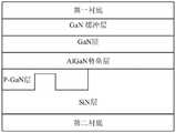
提供第一衬底,并在所述第一衬底表面生长外延结构,所述外延结构 包括依次生长于第一衬底表面的GaN缓冲层、GaN层、AlGaN势垒层和p-GaN 层,所述外延结构包括第一预设区域和第二预设区域;A first substrate is provided, and an epitaxial structure is grown on the surface of the first substrate, the epitaxial structure includes a GaN buffer layer, a GaN layer, an AlGaN barrier layer and a p-GaN layer sequentially grown on the surface of the first substrate, The epitaxial structure includes a first preset area and a second preset area;
通过刻蚀去除所述第一预设区域内的p-GaN层,并在所述第二预设区域 内刻蚀p-GaN层远离AlGaN势垒层一侧的表面,形成第一凹槽;Remove the p-GaN layer in the first preset region by etching, and etch the surface of the p-GaN layer away from the AlGaN barrier layer in the second preset region to form a first groove;
在p-GaN层远离AlGaN势垒层一侧的表面沉积形成SiN层,且至少部分 SiN层与所述GaN层远离GaN缓冲层的一侧表面相接触;A SiN layer is deposited on the surface of the p-GaN layer away from the AlGaN barrier layer, and at least part of the SiN layer is in contact with the surface of the GaN layer away from the GaN buffer layer;
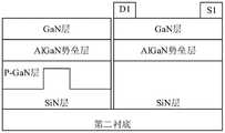
在SiN层远离所述第一衬底一侧的表面键合形成第二衬底,并在沿垂直 于第一衬底所在平面的方向翻转样品之后,刻蚀掉所述第一衬底及所述GaN 缓冲层;A second substrate is formed by bonding the surface of the SiN layer away from the first substrate, and after the sample is turned over in a direction perpendicular to the plane of the first substrate, the first substrate and all substrates are etched away. the GaN buffer layer;
刻蚀所述第二预设区域中靠近所述第一预设区域一侧的至少部分GaN 层、AlGaN势垒层、p-GaN层和SiN层,形成电隔离区域、以及分别位于所 述电隔离区域两侧的n沟道器件有源区和p沟道器件有源区;Etching at least part of the GaN layer, the AlGaN barrier layer, the p-GaN layer and the SiN layer in the second preset region close to one side of the first preset region to form electrical isolation regions, and Active regions for n-channel devices and active regions for p-channel devices on both sides of the isolation region;
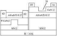
在所述n沟道器件中GaN层远离所述AlGaN势垒层的一侧表面制作第一 源电极和第一漏电极后,刻蚀所述p沟道器件的GaN层和至少部分AlGaN势 垒层,并在p-GaN层远离第二衬底的一侧制作第二源电极和第二漏电极;After forming the first source electrode and the first drain electrode on the surface of the n-channel device on the side of the GaN layer away from the AlGaN barrier layer, the GaN layer of the p-channel device and at least part of the AlGaN barrier are etched layer, and make a second source electrode and a second drain electrode on the side of the p-GaN layer away from the second substrate;
刻蚀所述n沟道器件中GaN层远离所述AlGaN势垒层一侧的表面,形 成第二凹槽,并在n沟道器件及p沟道器件远离所述第二衬底的一侧表面 沉积Al2O3;Etching the surface of the GaN layer in the n-channel device away from the AlGaN barrier layer to form a second groove, and on the side of the n-channel device and the p-channel device away from the second substrate Surface deposition of Al2 O3 ;
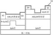
刻蚀去除覆盖于n沟道器件以外的Al2O3,并在p沟道器件中AlGaN 势垒层远离第二衬底的一侧表面刻蚀形成第三凹槽后,制作n沟道器件的 第一栅电极和p沟道器件的第二栅电极;The Al2 O3 covering outside the n-channel device is removed by etching, and the surface of the AlGaN barrier layer in the p-channel device is etched away from the second substrate to form a third groove, and the n-channel device is fabricated The first gate electrode and the second gate electrode of the p-channel device;
在所述n沟道器件及所述p沟道器件远离第二衬底的一侧表面生长SiN 保护层,并在SiN保护层上光刻金属互联层开孔区后引出第一源电极、第 一漏电极、第一栅电极、第二源电极、第二漏电极和第二栅电极,并使第 一漏电极与第二漏电极电连接,得到所述N面GaN基p、n沟道器件集成 结构。A SiN protective layer is grown on the surface of the n-channel device and the p-channel device away from the second substrate, and the first source electrode, the first source electrode and the third a drain electrode, a first gate electrode, a second source electrode, a second drain electrode and a second gate electrode, and the first drain electrode and the second drain electrode are electrically connected to obtain the N-face GaN-based p, n-channel Device integration structure.
在本发明的一个实施例中,所述在SiN层远离所述第一衬底一侧的表面 键合形成第二衬底的步骤之前,还包括:In an embodiment of the present invention, before the step of forming the second substrate by bonding the surface of the SiN layer on the side away from the first substrate, the method further includes:
利用化学机械抛光工艺对所述SiN层远离第一衬底一侧的表面进行抛 光。The surface of the SiN layer on the side away from the first substrate is polished by a chemical mechanical polishing process.
在本发明的一个实施例中,所述在沿垂直于第一衬底所在平面的方向 翻转样品之后,刻蚀掉所述第一衬底及所述GaN缓冲层的步骤,包括:In one embodiment of the present invention, the step of etching off the first substrate and the GaN buffer layer after turning the sample in a direction perpendicular to the plane of the first substrate includes:
沿垂直于第一衬底所在平面的方向翻转样品后,在上电极功率为 250~350W、下电极功率为20~40W、压力为5mTorr、SF6流量为50sccm的条 件下,刻蚀掉所述第一衬底;After flipping the sample in the direction perpendicular to the plane of the first substrate, under the conditions that the power of the upper electrode is 250-350W, the power of the lower electrode is 20-40W, the pressure is 5mTorr, and the flow rate ofSF6 is 50sccm, the said a first substrate;
在上电极功率为40~60W、下电极功率为20~30W、压强为5mTorr、Cl2流量为8sccm、BCl3流量为20sccm的条件下,刻蚀掉所述GaN缓冲层。The GaN buffer layer is etched away under the conditions of upper electrode power of 40-60 W, lower electrode power of 20-30 W, pressure of 5 mTorr, flow of Cl2 of 8 sccm, and flow of BCl3 of 20 sccm.
在本发明的一个实施例中,所述第二预设区域包括靠近所述第一预设 区域的子区域;In an embodiment of the present invention, the second preset area includes a sub-area close to the first preset area;
所述刻蚀所述第二预设区域中靠近所述第一预设区域一侧的至少部分 GaN层、AlGaN势垒层、p-GaN层和SiN层,形成电隔离区域、以及分别位 于所述电隔离区域两侧的n沟道器件有源区和p沟道器件有源区的步骤,包 括:The etching of at least part of the GaN layer, the AlGaN barrier layer, the p-GaN layer and the SiN layer on the side of the second preset region close to the first preset region to form an electrical isolation region, and The steps of the active region of the n-channel device and the active region of the p-channel device on both sides of the electrical isolation region include:
对样品进行光刻胶的涂胶和甩胶;Apply photoresist to the sample and spray it;
将样品放入光刻机中,对所述子区域内的光刻胶进行曝光,并将曝光 后的样品放入显影液中,移除所述子区域内的光刻胶;Put the sample into the photolithography machine, expose the photoresist in the sub-region, and put the exposed sample into the developing solution, and remove the photo-resist in the sub-region;
利用电感耦合等离子体ICP工艺依次刻蚀所述子区域内的GaN层、 AlGaN势垒层和p-GaN层,实现有源区的台面隔离,形成电隔离区域、以及 分别位于所述电隔离区域两侧的n沟道器件有源区和p沟道器件有源区。The inductively coupled plasma ICP process is used to sequentially etch the GaN layer, the AlGaN barrier layer and the p-GaN layer in the sub-region to realize the mesa isolation of the active region, forming an electrical isolation region, and an electrical isolation region respectively located in the electrical isolation region Active regions for n-channel devices and active regions for p-channel devices on both sides.
在本发明的一个实施例中,所述刻蚀所述n沟道器件中GaN层远离所 述AlGaN势垒层一侧的表面,形成第二凹槽,并在n沟道器件及p沟道器 件远离所述第二衬底的一侧表面沉积Al2O3的步骤,包括:In one embodiment of the present invention, the etching of the surface of the GaN layer in the n-channel device on the side away from the AlGaN barrier layer forms a second groove, and the n-channel device and the p-channel The step of depositing Al2 O3 on the side surface of the device away from the second substrate includes:
在上电极功率为15~25W、下电极功率为3~5W、压力为5mTorr、Cl2流量为4sccm、BCl3流量为10sccm的条件下,刻蚀所述n沟道器件中GaN 层远离所述AlGaN势垒层一侧的表面,形成第二凹槽;Under the conditions that the power of the upper electrode is 15-25 W, the power of the lower electrode is 3-5 W, the pressure is 5 mTorr, the flow rate of Cl2 is 4 sccm, and the flow rate of BCl3 is 10 sccm, the GaN layer in the n-channel device is etched away from the A surface on one side of the AlGaN barrier layer forms a second groove;
利用原子层沉积ALD技术,在n沟道器件及p沟道器件远离所述第二 衬底的一侧表面沉积厚度为20nm的Al2O3。Using atomic layer deposition (ALD) technology, Al2 O3 with a thickness of 20 nm is deposited on the surfaces of the n-channel device and the p-channel device on one side away from the second substrate.
在本发明的一个实施例中,所述第二凹槽包括与所述第一衬底平行的 第一表面;In one embodiment of the present invention, the second groove includes a first surface parallel to the first substrate;
其中,沿垂直于第一衬底所在平面的方向,所述第一表面与所述AlGaN 势垒层之间的距离为10nm。Wherein, along the direction perpendicular to the plane of the first substrate, the distance between the first surface and the AlGaN barrier layer is 10 nm.
在本发明的一个实施例中,所述刻蚀去除覆盖于n沟道器件以外的 Al2O3,并在p沟道器件中AlGaN势垒层远离第二衬底的一侧表面刻蚀形成 第三凹槽后,制作n沟道器件的第一栅电极和p沟道器件的第二栅电极的 步骤,包括:In an embodiment of the present invention, the etching removes the Al2 O3 covering the n-channel device, and the AlGaN barrier layer in the p-channel device is formed by etching on the side of the surface away from the second substrate After the third groove, the steps of fabricating the first gate electrode of the n-channel device and the second gate electrode of the p-channel device include:
在上电极功率为100~200W、下电极功率为30~40W、压强为10mTorr、 CF4流量为45sccm的条件下,刻蚀除去覆盖于n沟道器件以外的Al2O3,露 出p沟道器件中的AlGaN势垒层、第二源电极、第二漏电极以及n沟道器 件中的第一源电极和第一漏电极;Under the conditions that the power of the upper electrode is 100-200 W, the power of the lower electrode is 30-40 W, the pressure is 10 mTorr, and the flow rate of CF4 is 45 sccm, the Al2 O3 covering the n-channel device is removed by etching, and the p-channel is exposed. an AlGaN barrier layer, a second source electrode, a second drain electrode in the device, and a first source electrode and a first drain electrode in an n-channel device;
在上电极功率为15~25W、下电极功率为3~5W、压强为5mTorr、Cl2流量为4sccm、BCl3流量为10sccm的条件下,在p沟道器件的AlGaN势垒 层远离第二衬底的一侧表面刻蚀形成第三凹槽;Under the condition that the power of the upper electrode is 15-25 W, the power of the lower electrode is 3-5 W, the pressure is 5 mTorr, the flow rate of Cl2 is 4 sccm, and the flow rate of BCl3 is 10 sccm, the AlGaN barrier layer of the p-channel device is far away from the second liner One side surface of the bottom is etched to form a third groove;
制作n沟道器件的第一栅电极和p沟道器件的第二栅电极。A first gate electrode for an n-channel device and a second gate electrode for a p-channel device are fabricated.
在本发明的一个实施例中,沿垂直于第一衬底所在平面的方向,所述 第一凹槽的正投影与所述第三凹槽的正投影重合。In an embodiment of the present invention, along a direction perpendicular to the plane of the first substrate, the orthographic projection of the first groove coincides with the orthographic projection of the third groove.
第二方面,本发明还提供一种N面GaN基p、n沟道器件集成结构,由上 述第一方面所述的N面GaN基p、n沟道器件集成结构的制备方法制得。In a second aspect, the present invention also provides an N-plane GaN-based p, n-channel device integrated structure, which is prepared by the method for preparing an N-plane GaN-based p, n-channel device integrated structure described in the first aspect.
与现有技术相比,本发明的有益效果在于:Compared with the prior art, the beneficial effects of the present invention are:
本发明提供了一种N面GaN基p、n沟道器件集成结构及其制备方法,由 于采用了N面AlGaN/GaN异质结制备p沟道器件,GaN沟道上层存在AlGaN 势垒层可以起到阻挡栅极漏电流的作用,因此制备过程中可以免去在栅极 金属与p-GaN沟道之间的绝缘介质,如Al2O3,进而避免沉积的绝缘层引入 固定电荷、以及和材料之间的界面电荷等问题,改善了p沟道器件的迁移率; 另外,N面GaN基材料制备的GaN基n沟道器件在高频方面相较于Ga面n沟道器件更有优势。因此,采用凹槽MIS结构制备N面的n沟增强型器件也具有 良好特性。N面增强型n沟器件与p沟器件的集成也使得GaN基互补逻辑结构 得以实现。The invention provides an N-face GaN-based p, n-channel device integrated structure and a preparation method thereof. Since the N-face AlGaN/GaN heterojunction is used to prepare the p-channel device, the presence of an AlGaN barrier layer on the upper layer of the GaN channel can prevent It plays the role of blocking the gate leakage current, so the insulating medium between the gate metal and the p-GaN channel, such as Al2 O3 , can be avoided during the preparation process, thereby avoiding the introduction of fixed charges into the deposited insulating layer, and Compared with Ga-surface n-channel devices, GaN-based n-channel devices prepared from N-face GaN-based materials have better high frequency than Ga-face n-channel devices. Advantage. Therefore, the n-channel enhancement mode device with the N-face fabricated by the recessed MIS structure also has good characteristics. The integration of N-surface enhancement mode n-channel devices and p-channel devices also enables the realization of GaN-based complementary logic structures.
以下将结合附图及实施例对本发明做进一步详细说明。The present invention will be further described in detail below with reference to the accompanying drawings and embodiments.
附图说明Description of drawings
图1是本发明实施例提供的N面GaN基p、n沟道器件集成结构的制 备方法的一种流程图;Fig. 1 is a kind of flow chart of the preparation method of N-face GaN-based p, n-channel device integrated structure provided in the embodiment of the present invention;
图2是本发明实施例提供的N面GaN基p、n沟道器件集成结构的制 备方法的一种示意图;Fig. 2 is a kind of schematic diagram of the preparation method of the integrated structure of N-plane GaN-based p, n-channel device provided in the embodiment of the present invention;
图3是本发明实施例提供的N面GaN基p、n沟道器件集成结构的制 备方法的另一种示意图;Fig. 3 is another schematic diagram of the preparation method of the N-plane GaN-based p, n-channel device integrated structure provided by the embodiment of the present invention;
图4是本发明实施例提供的N面GaN基p、n沟道器件集成结构的制 备方法的另一种示意图;Fig. 4 is another schematic diagram of the preparation method of the N-plane GaN-based p, n-channel device integrated structure provided by the embodiment of the present invention;
图5是本发明实施例提供的N面GaN基p、n沟道器件集成结构的制 备方法的另一种示意图;Fig. 5 is another schematic diagram of the preparation method of the N-plane GaN-based p, n-channel device integrated structure provided by the embodiment of the present invention;
图6是本发明实施例提供的N面GaN基p、n沟道器件集成结构的制 备方法的另一种示意图;Fig. 6 is another schematic diagram of the preparation method of the integrated structure of N-plane GaN-based p, n-channel device provided by the embodiment of the present invention;
图7是本发明实施例提供的N面GaN基p、n沟道器件集成结构的制 备方法的另一种示意图;Fig. 7 is another schematic diagram of the preparation method of the N-plane GaN-based p, n-channel device integrated structure provided by the embodiment of the present invention;
图8是本发明实施例提供的N面GaN基p、n沟道器件集成结构的制 备方法的另一种示意图;Fig. 8 is another schematic diagram of the preparation method of the N-plane GaN-based p, n-channel device integrated structure provided by the embodiment of the present invention;
图9是本发明实施例提供的N面GaN基p、n沟道器件集成结构的制 备方法的另一种示意图;Fig. 9 is another schematic diagram of the preparation method of the N-plane GaN-based p, n-channel device integrated structure provided by the embodiment of the present invention;
图10是本发明实施例提供的N面GaN基p、n沟道器件集成结构的制 备方法的另一种示意图;Fig. 10 is another schematic diagram of the preparation method of the N-plane GaN-based p, n-channel device integrated structure provided by the embodiment of the present invention;
图11是本发明实施例提供的N面GaN基p、n沟道器件集成结构的制 备方法的另一种示意图;Fig. 11 is another schematic diagram of the preparation method of the N-plane GaN-based p, n-channel device integrated structure provided by the embodiment of the present invention;
图12是本发明实施例提供的N面GaN基p、n沟道器件集成结构的制 备方法的另一种示意图;Fig. 12 is another schematic diagram of the preparation method of the N-plane GaN-based p, n-channel device integrated structure provided by the embodiment of the present invention;
图13是本发明实施例提供的N面GaN基p、n沟道器件集成结构的制 备方法的另一种示意图;Fig. 13 is another schematic diagram of the preparation method of the N-plane GaN-based p, n-channel device integrated structure provided by the embodiment of the present invention;
图14是本发明实施例提供的N面GaN基p、n沟道器件集成结构的制 备方法的另一种示意图;Fig. 14 is another schematic diagram of the preparation method of the N-plane GaN-based p, n-channel device integrated structure provided by the embodiment of the present invention;
图15是本发明实施例提供的N面GaN基p、n沟道器件集成结构的制 备方法的另一种示意图。Fig. 15 is another schematic diagram of the preparation method of the N-plane GaN-based p, n-channel device integrated structure provided by the embodiment of the present invention.
具体实施方式Detailed ways
下面结合具体实施例对本发明做进一步详细的描述,但本发明的实施 方式不限于此。The present invention will be described in further detail below in conjunction with specific embodiments, but the embodiments of the present invention are not limited thereto.
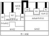
图1是本发明实施例提供的N面GaN基p、n沟道器件集成结构的制备方法的 一种流程图,图2-15是本发明实施例提供的N面GaN基p、n沟道器件集成结构的 制备方法的一种示意图。请参见图1-15,本发明实施例提供了一种N面GaN基p、 n沟道器件集成结构的制备方法,包括:FIG. 1 is a flowchart of a method for preparing an N-plane GaN-based p, n-channel device integrated structure provided by an embodiment of the present invention, and FIGS. 2-15 are N-plane GaN-based p, n-channel device provided by an embodiment of the present invention. A schematic diagram of the preparation method of the device integrated structure. Referring to FIGS. 1-15 , an embodiment of the present invention provides a method for fabricating an N-plane GaN-based p, n-channel device integrated structure, including:
S1、提供第一衬底,并在第一衬底表面生长外延结构,外延结构包括 依次生长于第一衬底表面的GaN缓冲层、GaN层、AlGaN势垒层和p-GaN层, 所述外延结构包括第一预设区域和第二预设区域;S1. Provide a first substrate, and grow an epitaxial structure on the surface of the first substrate, where the epitaxial structure includes a GaN buffer layer, a GaN layer, an AlGaN barrier layer and a p-GaN layer sequentially grown on the surface of the first substrate, the The epitaxial structure includes a first preset area and a second preset area;
S2、通过刻蚀去除第一预设区域内的p-GaN层,并在第二预设区域内刻 蚀p-GaN层远离AlGaN势垒层一侧的表面,形成第一凹槽10;S2, remove the p-GaN layer in the first preset area by etching, and etch the p-GaN layer away from the surface of the AlGaN barrier layer side in the second preset area to form the
S3、在p-GaN层远离AlGaN势垒层一侧的表面沉积形成SiN层,且至少 部分SiN层与GaN层远离GaN缓冲层的一侧表面相接触;S3, deposit and form the SiN layer on the surface of the p-GaN layer away from the AlGaN barrier layer, and at least part of the SiN layer is in contact with the surface of the GaN layer away from the GaN buffer layer;
S4、在SiN层远离第一衬底一侧的表面键合形成第二衬底,并在沿垂直 于第一衬底所在平面的方向翻转样品之后,刻蚀掉第一衬底及GaN缓冲层;S4. Bond the surface of the SiN layer away from the first substrate to form a second substrate, and after flipping the sample in a direction perpendicular to the plane of the first substrate, the first substrate and the GaN buffer layer are etched away ;
S5、刻蚀第二预设区域中靠近第一预设区域一侧的至少部分GaN层、AlGaN势垒层、p-GaN层和SiN层,形成电隔离区域、以及分别位于电隔离 区域两侧的n沟道器件有源区和p沟道器件有源区;S5. Etch at least part of the GaN layer, the AlGaN barrier layer, the p-GaN layer, and the SiN layer in the second preset region close to one side of the first preset region to form an electrical isolation region and on both sides of the electrical isolation region respectively n-channel device active region and p-channel device active region;
S6、在n沟道器件中GaN层远离AlGaN势垒层的一侧表面制作第一源电 极和第一漏电极后,刻蚀p沟道器件的GaN层和至少部分AlGaN势垒层,并 在p-GaN层远离第二衬底的一侧制作第二源电极和第二漏电极;S6. After fabricating the first source electrode and the first drain electrode on the surface of the GaN layer far away from the AlGaN barrier layer in the n-channel device, the GaN layer and at least part of the AlGaN barrier layer of the p-channel device are etched, and the A second source electrode and a second drain electrode are formed on the side of the p-GaN layer away from the second substrate;
S7、刻蚀n沟道器件中GaN层远离AlGaN势垒层一侧的表面,形成第 二凹槽20,并在n沟道器件及p沟道器件远离第二衬底的一侧表面沉积 Al2O3;S7, etching the surface of the GaN layer in the n-channel device away from the AlGaN barrier layer to form a
S8、刻蚀去除覆盖于n沟道器件以外的Al2O3,并在p沟道器件中AlGaN 势垒层远离第二衬底的一侧表面刻蚀形成第三凹槽40后,制作n沟道器件 的第一栅电极G1和p沟道器件的第二栅电极G2;S8. Etching and removing the Al2 O3 covering the n-channel device, and etching the surface of the AlGaN barrier layer away from the second substrate to form the
S9、在n沟道器件及p沟道器件远离第二衬底的一侧表面生长SiN保 护层,并在SiN保护层上光刻金属互联层开孔区后引出第一源电极、第一 漏电极、第一栅电极G1、第二源电极、第二漏电极和第二栅电极G2,并 使第一漏电极D1与第二漏电极D2电连接,得到N面GaN基p、n沟道器 件集成结构。S9, growing a SiN protective layer on the side surface of the n-channel device and the p-channel device away from the second substrate, and lithography the metal interconnection layer opening area on the SiN protective layer to lead out the first source electrode and the first leakage current electrode, the first gate electrode G1, the second source electrode, the second drain electrode and the second gate electrode G2, and the first drain electrode D1 and the second drain electrode D2 are electrically connected to obtain an N-face GaN-based p, n-channel Device integration structure.
本实施例中,第一衬底可以为Si衬底,采用 MOCVD(Metal-organic ChemicalVapor Deposition,金属有机化合物化学气 相沉淀)法在第一衬底表面生长外延结构,可选地,在图2所示视角下,外 延结构自下而上依次为GaN缓冲层、GaN层、AlGaN势垒层和p-GaN层。In this embodiment, the first substrate may be a Si substrate, and an MOCVD (Metal-organic Chemical Vapor Deposition) method is used to grow an epitaxial structure on the surface of the first substrate. Optionally, as shown in FIG. 2 From the bottom to top, the epitaxial structure is a GaN buffer layer, a GaN layer, an AlGaN barrier layer, and a p-GaN layer in order from the viewing angle.
具体地,步骤S2中,将样品在200℃下烘烤5分钟,然后置于匀胶机 上,在样品第一衬底的表面滴取EPI621光刻胶,匀胶时可先以500rpm/min 的转速甩胶5秒、再以3500rpm/min的转速甩胶40秒,接着在90℃下烘烤60秒;之后,对样品进行曝光、显影,并用超纯水冲洗、氮气吹干。进一 步地,在上电极功率为40~60W、下电极功率10~20W、压强为5mTorr、Cl2/BCl3流量为8/20sccm的条件下,使用氯基ICP刻蚀p-GaN层远离AlGaN 势垒层一侧的表面,在第二预设区域内形成第一凹槽10;可选地,沿垂直 于第一衬底所在平面的方向,第一凹槽10处剩余的p-GaN层厚度约为 10~30nm。Specifically, in step S2, the sample is baked at 200° C. for 5 minutes, then placed on a glue dispenser, and EPI621 photoresist is dropped on the surface of the first substrate of the sample. Spin for 5 seconds at a rotational speed, then spin at 3500 rpm/min for 40 seconds, and bake at 90°C for 60 seconds; after that, expose and develop the sample, rinse with ultrapure water, and dry with nitrogen. Further, under the conditions that the power of the upper electrode is 40-60 W, the power of the lower electrode is 10-20 W, the pressure is 5 mTorr, and the Cl2 /BCl3 flow rate is 8/20 sccm, the p-GaN layer is etched away from the AlGaN potential using chlorine-based ICP etching. On the surface of one side of the barrier layer, a
需要说明的是,本实施例中第一预设区域内的p-GaN层也是经光刻、 刻蚀工艺来去除,且刻蚀的条件与上述第一凹槽10的刻蚀条件相同,故此 处不再赘述。It should be noted that in this embodiment, the p-GaN layer in the first preset region is also removed by photolithography and etching processes, and the etching conditions are the same as the etching conditions of the
步骤S3中,利用等离子体增强化学气相沉积PECVD工艺,在p-GaN 层远离AlGaN势垒层一侧的表面沉积SiN,如图4所示,SiN层填充第一 凹槽10,而在第一预设区域的范围内,SiN层与GaN层远离GaN缓冲层的 一侧表面接触。进一步地,在SiN层远离第一衬底一侧的表面键合形成第 二衬底,然后沿垂直于第一衬底所在平面的方向翻转样品,即在图5所示 视角下,上下翻转该样品,然后依次刻蚀掉第一衬底和GaN缓冲层。In step S3, using the plasma enhanced chemical vapor deposition (PECVD) process, SiN is deposited on the surface of the p-GaN layer on the side away from the AlGaN barrier layer. As shown in FIG. Within the range of the preset area, the SiN layer is in contact with the surface of the side of the GaN layer away from the GaN buffer layer. Further, a second substrate is formed by bonding the surface of the SiN layer away from the first substrate, and then the sample is turned over in a direction perpendicular to the plane of the first substrate, that is, under the viewing angle shown in FIG. 5, the sample is turned upside down. sample, and then the first substrate and the GaN buffer layer are sequentially etched away.
请继续参见图7,上述步骤S5中,将第二预设区域中靠近第一预设区 域的位置刻蚀形成电隔离区域,那么图7中电隔离区域的右侧部分为n沟 道器件有源区、左侧部分为p沟道器件有源区。进一步地,如图8-9所示, 分别制作n沟道器件和p沟道器件的源、漏电极,n沟道器件的第一源电极 和第一漏电极相对设置于GaN层远离AlGaN势垒层的一侧表面,p沟道器 件的第二源电极和第二漏电极相对设置于p-GaN层远离第二衬底的一侧。Please continue to refer to FIG. 7. In the above step S5, an electrical isolation area is formed by etching a position in the second preset area close to the first preset area, then the right part of the electrical isolation area in FIG. The source region and the left part are the active regions of the p-channel device. Further, as shown in Figures 8-9, the source and drain electrodes of the n-channel device and the p-channel device are respectively fabricated, and the first source electrode and the first drain electrode of the n-channel device are relatively arranged on the GaN layer away from the AlGaN potential. On one side surface of the barrier layer, the second source electrode and the second drain electrode of the p-channel device are disposed opposite to the side of the p-GaN layer away from the second substrate.
请参见图10-13,n、p沟道器件的源电极和漏电极制作完成后,对n 沟道器件中GaN层远离AlGaN势垒层一侧的表面进行凹槽刻蚀,得到第二 凹槽20,然后在n沟道器件及p沟道器件的表面沉积氧化铝30,接着保留 n沟道器件中GaN层远离AlGaN势垒层一侧表面的氧化铝30、刻蚀去除其 他区域的氧化铝30,并在p沟道器件中AlGaN势垒层远离第二衬底的一侧 表面刻蚀第三凹槽40,即可得到p沟道器件的栅极凹槽。Please refer to Figure 10-13. After the source and drain electrodes of the n- and p-channel devices are fabricated, groove etching is performed on the surface of the n-channel device on the side of the GaN layer away from the AlGaN barrier layer to obtain a second recess.
进一步地,如图14-15所示,同时制作n、p沟道器件的栅电极,而后 生长SiN保护层,并在SiN保护层上光刻金属互联层开孔区后引出各个电 极,并使第一漏电极D1与第二漏电极D2电连接,得到N面GaN基p、n 沟道器件集成结构。Further, as shown in Figures 14-15, gate electrodes of n and p-channel devices are fabricated at the same time, and then a SiN protective layer is grown, and each electrode is drawn out after the opening area of the metal interconnection layer is photoetched on the SiN protective layer. The first drain electrode D1 and the second drain electrode D2 are electrically connected to obtain an N-plane GaN-based p, n-channel device integrated structure.
应当理解,N面GaN基HFET p沟道器件由于存在AlGaN层,在制备 工艺中可以免去在栅极金属与p-GaN沟道之间的绝缘介质如Al2O3,因此可 以避免沉积的绝缘层引入固定电荷、以及与材料之间的界面电荷等问题, 从而改善p沟道器件迁移率;同时,采用凹槽MIS结构制备N面的n沟增 强型器件也具有良好特性,增强型n沟器件与p沟器件的集成,使得互补逻辑结构得以实现。It should be understood that, due to the presence of the AlGaN layer in the N-plane GaN-based HFET p-channel device, the insulating medium such as Al2 O3 between the gate metal and the p-GaN channel can be avoided during the preparation process, so the deposition process can be avoided. The insulating layer introduces problems such as fixed charges and interfacial charges with materials, thereby improving the mobility of p-channel devices; at the same time, the n-channel enhancement-type devices with the N-surface prepared by the groove MIS structure also have good characteristics. The integration of channel devices and p-channel devices enables the realization of complementary logic structures.
可选地,在SiN层远离第一衬底一侧的表面键合形成第二衬底的步骤之 前,还包括:Optionally, before the step of bonding the surface of the SiN layer away from the first substrate side to form the second substrate, it also includes:
利用化学机械抛光工艺对SiN层远离第一衬底一侧的表面进行抛光。The surface of the SiN layer on the side away from the first substrate is polished by a chemical mechanical polishing process.
本实施例中,在键合第二衬底之前,先通过化学机械抛光工艺对SiN层 远离的上表面进行抛光,此种设计方式能够使SiN层与第二衬底接触的表面 更加光滑,从而避免第二衬底与SiN层键合不稳定,防止后续翻转样品时第 二衬底因键合不稳定而脱落。In this embodiment, before bonding the second substrate, the upper surface of the SiN layer away from the SiN layer is polished by a chemical mechanical polishing process. This design method can make the surface of the SiN layer in contact with the second substrate smoother, so that the To avoid unstable bonding between the second substrate and the SiN layer, and to prevent the second substrate from falling off due to unstable bonding when the sample is subsequently turned over.
请继续参见图6,上述步骤S4中,在沿垂直于第一衬底所在平面的方向 翻转样品之后,刻蚀掉第一衬底及GaN缓冲层的步骤,包括:Please continue to refer to Fig. 6, in the above-mentioned step S4, after flipping the sample along the direction perpendicular to the plane where the first substrate is located, the steps of etching off the first substrate and the GaN buffer layer include:
S401、沿垂直于第一衬底所在平面的方向翻转样品后,在上电极功率 为250~350W、下电极功率为20~40W、压力为5mTorr、SF6流量为50sccm的 条件下,刻蚀掉第一衬底;S401, after flipping the sample in a direction perpendicular to the plane where the first substrate is located, under the conditions that the power of the upper electrode is 250-350W, the power of the lower electrode is 20-40W, the pressure is 5mTorr, and the flow rate ofSF6 is 50sccm, etch away a first substrate;
S402、在上电极功率为40~60W、下电极功率为20~30W、压强为5mTorr、 Cl2流量为8sccm、BCl3流量为20sccm的条件下,刻蚀掉GaN缓冲层。S402 , under the conditions that the power of the upper electrode is 40-60 W, the power of the lower electrode is 20-30 W, the pressure is 5 mTorr, the flow rate of Cl2 is 8 sccm, and the flow rate of BCl3 is 20 sccm, the GaN buffer layer is etched away.
请参见图5-7,,第二预设区域包括靠近第一预设区域的子区域;5-7, the second preset area includes a sub-area close to the first preset area;
上述步骤S5中,刻蚀第二预设区域中靠近第一预设区域一侧的至少部 分GaN层、AlGaN势垒层、p-GaN层和SiN层,形成电隔离区域、以及分别 位于电隔离区域两侧的n沟道器件有源区和p沟道器件有源区的步骤,包括:In the above-mentioned step S5, at least part of the GaN layer, the AlGaN barrier layer, the p-GaN layer and the SiN layer on the side of the second preset region close to the first preset region are etched to form an electrical isolation region, which is located in the electrical isolation region respectively. The steps of the active region of the n-channel device and the active region of the p-channel device on both sides of the region include:
S501、对样品进行光刻胶的涂胶和甩胶;S501, applying photoresist to the sample and spraying it;
S502、将样品放入光刻机中,对子区域内的光刻胶进行曝光,并将曝 光后的样品放入显影液中,移除子区域内的光刻胶;S502, put the sample into the photolithography machine, expose the photoresist in the subregion, and put the exposed sample into the developing solution, remove the photoresist in the subregion;
S503、利用电感耦合等离子体ICP工艺依次刻蚀子区域内的GaN层、 AlGaN势垒层和p-GaN层,实现有源区的台面隔离,形成电隔离区域、以及 分别位于电隔离区域两侧的n沟道器件有源区和p沟道器件有源区。S503 , sequentially etching the GaN layer, the AlGaN barrier layer and the p-GaN layer in the sub-region by using an inductively coupled plasma ICP process to achieve mesa isolation in the active region, forming an electrical isolation region and two sides of the electrical isolation region respectively The n-channel device active region and the p-channel device active region.
具体而言,首先将样品放在200℃的热板上烘烤,进行光刻胶的涂胶和 甩胶,再将样品放在90℃的热板上烘烤,其中,甩胶转速可以为3500转/min; 接着,将样品放入光刻机中对子区域内的光刻胶进行曝光后,将完成曝光 的样品放入显影液中以移除电隔离区域内的光刻胶,并对其进行超纯水冲 洗和氮气吹干。Specifically, the sample is first baked on a hot plate at 200°C, and the photoresist is applied and ejected, and then the sample is placed on a hot plate at 90°C for baking. The rotational speed of glue rejection can be 3500 rpm; then, put the sample into the photolithography machine to expose the photoresist in the sub-region, put the exposed sample into the developing solution to remove the photoresist in the electrically isolated area, and It was rinsed with ultrapure water and dried with nitrogen.
进一步地,对光刻后的子区域进行刻蚀。首先,利用ICP工艺依次刻 蚀子区域内的GaN层、AlGaN势垒层、p-GaN层和SiN层,实现有源区的 台面隔离;然后,将样品依次放入丙酮溶液、剥离液、丙酮溶液和乙醇溶 液中进行清洗,以移除电隔离区域外的光刻胶;最后,用超纯水冲洗样品 并用氮气吹干。Further, the sub-regions after photolithography are etched. First, the GaN layer, AlGaN barrier layer, p-GaN layer and SiN layer in the sub-region are etched sequentially by ICP process to achieve mesa isolation in the active region; then, the sample is placed in acetone solution, stripping solution, acetone solution and ethanol solution to remove the photoresist outside the electrically isolated areas; finally, the samples were rinsed with ultrapure water and blown dry with nitrogen.
请继续参见图8-10,在n沟道器件中GaN层远离AlGaN势垒层的一侧 表面制作第一源电极和第一漏电极后,刻蚀p沟道器件的GaN层和至少部 分AlGaN势垒层,并在p-GaN层远离第二衬底的一侧制作第二源电极和第 二漏电极的步骤,包括:Please continue to refer to FIGS. 8-10. After the first source electrode and the first drain electrode are formed on the surface of the GaN layer on the side of the n-channel device away from the AlGaN barrier layer, the GaN layer and at least part of the AlGaN layer of the p-channel device are etched barrier layer, and the steps of forming a second source electrode and a second drain electrode on the side of the p-GaN layer away from the second substrate include:
S601、光刻第一源电极区域和第一漏电极区域:S601, photolithography the first source electrode region and the first drain electrode region:
首先,将样品置于200℃的热板上烘烤,在GaN层上进行剥离胶的涂 胶和甩胶,可选地,以2000转/min的转速甩胶40s、甩胶厚度为0.35μm, 接着再用热板烘烤样品;然后,在剥离胶上进行EPI621光刻胶的涂胶和甩 胶,以5000转/min的转速甩胶30秒、甩胶厚度为0.77μm,之后用热板烘 烤;将完成涂胶和甩胶的样品放入光刻机中,对第一源电极区域和第一漏 电极区域内的光刻胶进行曝光;最后,将完成曝光的样品放入显影液中, 移除第一源电极区域和第一漏电极区域内的光刻胶、剥离胶,对其进行超 纯水冲洗和氮气吹干。First, the sample was baked on a hot plate at 200°C, and the release adhesive was applied and ejected on the GaN layer. , and then bake the sample with a hot plate; then, carry out the coating and gluing of EPI621 photoresist on the peeling glue, and the glue is spun at a speed of 5000 rpm for 30 seconds, and the thickness of the glue is 0.77 μm. Board baking; put the samples that have been coated and spun into the photolithography machine, and expose the photoresist in the first source electrode area and the first drain electrode area; finally, put the exposed samples into the development In the liquid, the photoresist and peeling glue in the first source electrode region and the first drain electrode region are removed, and they are rinsed with ultrapure water and dried with nitrogen.
S602、蒸发第一源电极S1和第一漏电极D1:S602, evaporating the first source electrode S1 and the first drain electrode D1:
首先,将有第一源电极光刻图形和第一漏电极光刻图形的样品放入α -plasma等离子体去胶机处理,然后将样品放入电子束蒸发台中,待电子束 蒸发台的反应腔室真空度达到2×10⁻⁶Torr后,在第一源电极区域和第一漏电 极区域内的GaN帽层、以及第一源电极区域和第一漏电极区域外的光刻胶 上蒸发欧姆金属,该欧姆金属可以是自下向上依次由Ti/Al/Ni/Au四层金属 组成的金属堆叠结构;接着,对完成欧姆金属蒸发的样品进行剥离,以移 除第一源电极区域和第一漏电极区域外的欧姆金属、光刻胶和剥离胶,并 用超纯水冲洗、氮气吹干;最后,将样品放入快速退火炉中进行退火处理, 形成第一源电极S1和第一漏电极D1;可选地,退火气氛为N2、退火温度 为800~860℃、退火时间为30~60s。First, put the sample with the lithographic pattern of the first source electrode and the lithographic pattern of the first drain electrode into the α-plasma plasma remover for processing, and then put the sample into the electron beam evaporation stage, and the reaction chamber of the electron beam evaporation stage After the chamber vacuum reaches 2×10⁻⁶ Torr, ohmic evaporation is performed on the GaN cap layer in the first source electrode region and the first drain electrode region, and the photoresist outside the first source electrode region and the first drain electrode region Metal, the ohmic metal can be a metal stack structure composed of Ti/Al/Ni/Au four-layer metals in sequence from bottom to top; then, the sample after ohmic metal evaporation is peeled off to remove the first source electrode region and the first source electrode area. The ohmic metal, photoresist and stripping glue outside the drain electrode area are rinsed with ultrapure water and dried with nitrogen gas; finally, the sample is placed in a rapid annealing furnace for annealing treatment to form the first source electrode S1 and the first leakage current. Pole D1; optionally, the annealing atmosphere is N2 , the annealing temperature is 800-860° C., and the annealing time is 30-60 s.
S603、刻蚀p沟道器件的GaN层:S603, etching the GaN layer of the p-channel device:
将样品放在200℃的热板上烘烤后,进行光刻胶的涂胶和甩胶,甩胶转 速为3500转/min,并将样品放在90℃的热板上烘烤;然后,将样品放入光 刻机中对p沟道器件部分区域内的光刻胶进行曝光,并将完成曝光后的样 品放入显影液中以移除电隔离区域内的光刻胶,对其进行超纯水冲洗和氮 气吹干;接着,利用ICP工艺依次刻蚀显影区域的GaN层直至AlGaN层, 刻蚀条件可以为:上电极功率15~25W、下电极功率3~5W、压强5mTorr, Cl2流量为4sccm、BCl3流量10sccm;将样品依次放入丙酮溶液、剥离液、 丙酮溶液和乙醇溶液中进行清洗,以移除电隔离区域外的光刻胶,最后用 超纯水冲洗样品并用氮气吹干。After baking the sample on a hot plate at 200 °C, the photoresist was applied and glued, the speed of the glue rejection was 3500 rpm, and the sample was baked on a hot plate at 90 °C; then, Put the sample into the photolithography machine to expose the photoresist in the partial area of the p-channel device, and put the exposed sample into the developer to remove the photoresist in the electrical isolation area, Rinse with ultrapure water and blow dry with nitrogen; then, use the ICP process to sequentially etch the GaN layer in the developed area until the AlGaN layer. The etching conditions can be: upper electrode power 15-25W, lower electrode power 3-5W, pressure 5mTorr, Cl2 The flow rate is 4 sccm, BCl3 The flow rate is 10 sccm; the sample is sequentially put into acetone solution, stripping solution, acetone solution and ethanol solution for cleaning to remove the photoresist outside the electrical isolation area, and finally rinse the sample with ultrapure water and use Blow dry with nitrogen.
S604、刻蚀p沟道器件的至少部分AlGaN势垒层:S604, etching at least part of the AlGaN barrier layer of the p-channel device:
首先,将样品放在200℃的热板上烘烤;然后,进行光刻胶的涂胶和甩 胶,其甩胶转速为3500转/min,并将样品放在90℃的热板上烘烤;接着, 将样品放入光刻机中对p沟道器件的源、漏部分区域内的光刻胶进行曝光, 再将完成曝光的样品放入显影液中以移除电隔离区域内的光刻胶,并对其 进行超纯水冲洗和氮气吹干。进一步地,利用ICP工艺刻蚀显影区域的 AlGaN层直到p-GaN层,刻蚀深度约为20nm,刻蚀条件可以为:上电极功 率15~25W、下电极功率3~5W、压强5mTorr、Cl2流量4sccm、BCl3流量 10sccm;之后,将样品依次放入丙酮溶液、剥离液、丙酮溶液和乙醇溶液 中进行清洗,移除电隔离区域外的光刻胶,再用超纯水冲洗样品并用氮气 吹干。First, bake the sample on a hot plate at 200°C; then, apply and spin the photoresist at a speed of 3500 rpm, and bake the sample on a hot plate at 90°C Bake; then, put the sample into the photolithography machine to expose the photoresist in the source and drain regions of the p-channel device, and then put the exposed sample into the developer to remove the photoresist in the electrical isolation region. The photoresist was rinsed with ultrapure water and dried with nitrogen. Further, the ICP process is used to etch the AlGaN layer in the developed area until the p-GaN layer, the etching depth is about 20 nm, and the etching conditions can be: upper electrode power 15-25 W, lower electrode power 3-5 W, pressure 5 mTorr, Cl2 flow 4 sccm, BCl3 flow 10 sccm; after that, put the sample into acetone solution, stripping solution, acetone solution and ethanol solution for cleaning, remove the photoresist outside the electrical isolation area, rinse the sample with ultrapure water and use Blow dry with nitrogen.
S605、光刻第二源电极区域和第二漏电极区域:S605, photolithography the second source electrode region and the second drain electrode region:
首先,将样品置于200℃的热板上烘烤,在样品上进行剥离胶的涂胶和 甩胶,可选地,以2000转/min的转速甩胶40s、甩胶厚度为0.35μm,接着 再用200℃的热板烘烤样品5min;然后,在剥离胶上进行EPI621光刻胶的 涂胶和甩胶,以5000转/min的转速甩胶30秒、甩胶厚度为0.77μm,之后 用900℃的热板烘烤1min;将完成涂胶和甩胶的样品放入光刻机中,对第 二源电极区域和第二漏电极区域内的光刻胶进行曝光;将完成曝光的样品 放入显影液中,移除第二源电极区域和第二漏电极区域内的光刻胶、剥离 胶,对其进行超纯水冲洗和氮气吹干。First, bake the sample on a hot plate at 200°C, and apply the peeling glue and sling on the sample. Then, bake the sample with a hot plate at 200°C for 5 min; then, apply and spin the EPI621 photoresist on the peeling adhesive, spin the adhesive at a speed of 5000 rpm for 30 seconds, and the thickness of the adhesive is 0.77 μm. After that, bake with a hot plate at 900°C for 1 min; put the samples that have been coated and spun into the photolithography machine, and expose the photoresist in the second source electrode area and the second drain electrode area; the exposure will be completed. The samples were put into the developer solution, the photoresist and peeling glue in the second source electrode region and the second drain electrode region were removed, and they were rinsed with ultrapure water and dried with nitrogen.
S606、蒸发第二源电极S2和第二漏电极D2:S606, evaporating the second source electrode S2 and the second drain electrode D2:
首先,将有第二源电极光刻图形和第二漏电极光刻图形的样品放入α -plasma等离子体去胶机处理,然后将样品放入电子束蒸发台中,待电子束 蒸发台的反应腔室真空度达到2×10⁻⁶Torr后,在第二源电极区域和第二漏电 极区域内的GaN帽层、以及第二源电极区域和第二漏电极区域外的光刻胶 上蒸发欧姆金属,该欧姆金属可以是自下向上依次由Ti/Al/Ni/Au四层金属 组成的金属堆叠结构;接着,对完成欧姆金属蒸发的样品进行剥离,以移 除第二源电极区域和第二漏电极区域外的欧姆金属、光刻胶和剥离胶,并 用超纯水冲洗、氮气吹干;最后,将样品放入快速退火炉中进行退火处理, 形成第二源电极S2和第二漏电极D2;示例性地,退火气氛为O2、退火温 度为500~550℃、退火时间为5~10min。First, put the sample with the lithography pattern of the second source electrode and the lithography pattern of the second drain electrode into the α-plasma plasma remover for processing, and then put the sample into the electron beam evaporation stage, and the reaction chamber of the electron beam evaporation stage After the chamber vacuum reaches 2×10⁻⁶ Torr, ohmic evaporation is performed on the GaN cap layer in the second source electrode region and the second drain electrode region, and the photoresist outside the second source electrode region and the second drain electrode region Metal, the ohmic metal can be a metal stack structure composed of four layers of Ti/Al/Ni/Au from bottom to top; then, the sample after ohmic metal evaporation is peeled off to remove the second source electrode region and the first The ohmic metal, photoresist and peeling glue outside the area of the second drain electrode are rinsed with ultrapure water and dried with nitrogen; finally, the sample is placed in a rapid annealing furnace for annealing treatment to form the second source electrode S2 and the second leakage current. Pole D2; exemplarily, the annealing atmosphere is O2 , the annealing temperature is 500-550° C., and the annealing time is 5-10 min.
上述步骤S7中,刻蚀n沟道器件中GaN层远离AlGaN势垒层一侧的 表面,形成第二凹槽20,并在n沟道器件及p沟道器件远离第二衬底的一 侧表面沉积Al2O3的步骤,包括:In the above step S7, the surface of the GaN layer in the n-channel device away from the AlGaN barrier layer is etched to form a
在上电极功率为15~25W、下电极功率为3~5W、压力为5mTorr、Cl2流量为4sccm、Bl3流量为10sccm的条件下,刻蚀n沟道器件中GaN层远 离AlGaN势垒层一侧的表面,形成第二凹槽20;Under the conditions that the power of the upper electrode is 15-25W, the power of the lower electrode is 3-5W, the pressure is 5 mTorr, the flow rate of Cl2 is 4 sccm, and the flow rate of Bl3 is 10 sccm, the GaN layer in the n-channel device is etched away from the AlGaN barrier layer. The surface of one side forms a
利用原子层沉积ALD技术,在n沟道器件及p沟道器件远离第二衬底 的一侧表面沉积厚度为20nm的Al2O3。Using atomic layer deposition (ALD) technology, Al2 O3 with a thickness of 20 nm was deposited on the surfaces of the n-channel device and the p-channel device on the side away from the second substrate.
本实施例中,第二凹槽20包括与第一衬底平行的第一表面;其中,沿 垂直于第一衬底所在平面的方向,第一表面与AlGaN势垒层之间的距离为 10nm;也就是说,将n沟道器件中GaN层刻蚀到剩余约10nm。In this embodiment, the
可选地,上述步骤S8中,刻蚀去除覆盖于n沟道器件以外的Al2O3, 并在p沟道器件中AlGaN势垒层远离第二衬底的一侧表面刻蚀形成第三凹 槽40后,制作n沟道器件的第一栅电极G1和p沟道器件的第二栅电极G2 的步骤,包括:Optionally, in the above step S8, the Al2 O3 covering outside the n-channel device is removed by etching, and the AlGaN barrier layer in the p-channel device is etched on the side of the surface away from the second substrate to form a third. After the
在上电极功率为100~200W、下电极功率为30~40W、压强为10mTorr、 CF4流量为45sccm的条件下,刻蚀除去覆盖于n沟道器件以外的Al2O3,露 出p沟道器件中的AlGaN势垒层、第二源电极S2、第二漏电极D2以及n 沟道器件中的第一源电极S1和第一漏电极D1;Under the conditions that the power of the upper electrode is 100-200 W, the power of the lower electrode is 30-40 W, the pressure is 10 mTorr, and the flow rate of CF4 is 45 sccm, the Al2 O3 covering the n-channel device is removed by etching, and the p-channel is exposed. The AlGaN barrier layer in the device, the second source electrode S2, the second drain electrode D2, and the first source electrode S1 and the first drain electrode D1 in the n-channel device;
在上电极功率为15~25W、下电极功率为3~5W、压强为5mTorr、Cl2流量为4sccm、BCl3流量为10sccm的条件下,在p沟道器件的AlGaN势垒 层远离第二衬底的一侧表面刻蚀形成第三凹槽40;Under the condition that the power of the upper electrode is 15-25 W, the power of the lower electrode is 3-5 W, the pressure is 5 mTorr, the flow rate of Cl2 is 4 sccm, and the flow rate of BCl3 is 10 sccm, the AlGaN barrier layer of the p-channel device is far away from the second liner One side surface of the bottom is etched to form a
制作n沟道器件的第一栅电极G1和p沟道器件的第二栅电极G2。The first gate electrode G1 of the n-channel device and the second gate electrode G2 of the p-channel device are fabricated.
可选地,沿垂直于第一衬底所在平面的方向,第一凹槽10的正投影与 第三凹槽40的正投影重合。应当理解,如果第一凹槽10与第三凹槽40没有 对齐的话,会导致制备的器件因第二栅电极下方对应的p-GaN层较厚而使器 件无法正常关断,没有正常特性。Optionally, along a direction perpendicular to the plane where the first substrate is located, the orthographic projection of the
本实施例中,n沟道器件的第一栅电极G1和p沟道器件的第二栅电极 G2可以同时制作,由于二者的制作工序相同,因此仅以第一栅电极G1为 例进行说明。具体地,将有第一栅电极G1光刻图形的样品放入α-plasma 等离子体去胶机中进行底膜处理后,将样品放入电子束蒸发台中,待电子 束蒸发台的反应腔室真空度达到2×10⁻⁶Torr时,在第一栅电极区域内外的光 刻胶上蒸发栅金属,该栅金属可以为自下向上依次由Ni和Au两层金属组 成的金属叠层结构;接着,对完成栅金属蒸发的样品进行剥离,以移除第 一栅电极区域外的栅金属、光刻胶和剥离胶;最后,用超纯水冲洗样品并 用氮气吹干。In this embodiment, the first gate electrode G1 of the n-channel device and the second gate electrode G2 of the p-channel device can be fabricated at the same time. Since the fabrication processes of the two are the same, only the first gate electrode G1 is used as an example for description. . Specifically, put the sample with the lithography pattern of the first gate electrode G1 into an α-plasma plasma remover for bottom film treatment, and then put the sample into the electron beam evaporation stage, and wait for the reaction chamber of the electron beam evaporation stage When the vacuum degree reaches 2×10⁻⁶ Torr, the gate metal is evaporated on the photoresist inside and outside the first gate electrode area, and the gate metal can be a metal stack structure consisting of Ni and Au two-layer metals sequentially from bottom to top; Next, the samples after the evaporation of the gate metal were stripped to remove the gate metal, photoresist and stripping glue outside the first gate electrode region; finally, the samples were rinsed with ultrapure water and dried with nitrogen gas.
上述步骤S9中,在n沟道器件及p沟道器件远离第二衬底的一侧表面 生长SiN保护层的步骤,包括:In above-mentioned step S9, the step of growing SiN protective layer on one side surface of n-channel device and p-channel device away from the second substrate, comprising:
以NH3和SiH4作为反应气体,在第二衬底温度为250℃、反应腔室压 力为600mTorr、射频功率为20~25W的条件下,利用PECVD工艺生长厚 度为200nm的SiN保护层。Using NH3 and SiH4 as reactive gases, under the conditions of a second substrate temperature of 250° C., a reaction chamber pressure of 600 mTorr, and a radio frequency power of 20-25 W, a SiN protective layer with a thickness of 200 nm was grown by PECVD process.
可选地,SiN保护层生长完成后,在SiN保护层上光刻金属互联层开孔 区后引出第一源电极S1、第一漏电极D1、第一栅电极G1、第二源电极S2、 第二漏电极D2和第二栅电极G2,并使第一漏电极D1与第二漏电极D2电 连接,得到N面GaN基p、n沟道器件集成结构的步骤,包括:Optionally, after the growth of the SiN protective layer is completed, the first source electrode S1, the first drain electrode D1, the first gate electrode G1, the second source electrode S2, the first source electrode S1, the first drain electrode D1, the first gate electrode G1, the second source electrode S2, The second drain electrode D2 and the second gate electrode G2, and the first drain electrode D1 and the second drain electrode D2 are electrically connected to obtain an N-face GaN-based p, n-channel device integrated structure, including:
光刻电极开孔。具体而言,首先将样品放在200℃的热板上烘烤,然后 进行光刻胶的涂胶和甩胶,本实施例可选择性使用EPI621胶,甩胶转速为 3500转/min,之后将样品放在90℃的热板上烘烤;接着,将样品放入光刻 机中对金属互联层开孔区域内的光刻胶进行曝光,并将曝光后的样品放入 显影液中以移除互联开孔区域内的光刻胶,对其进行超纯水冲洗和氮气吹 干。Photolithographic electrode openings. Specifically, the sample is first baked on a hot plate at 200°C, and then the photoresist is applied and ejected. In this embodiment, EPI621 glue can be selectively used, and the ejection speed is 3500 rpm. The sample was baked on a hot plate at 90 °C; then, the sample was placed in a photolithography machine to expose the photoresist in the open area of the metal interconnection layer, and the exposed sample was placed in a developer to The photoresist in the interconnect opening area was removed, rinsed with ultrapure water and dried with nitrogen.
光刻完成后,以CF4和O2为反应气体、在反应腔室压力l0mTorr、上 电极射频功率为80~100w、下电极射频功率为l0~20W的条件下进行ICP 刻蚀,移除互联开孔区域内200nm厚的SiN保护层。After the lithography is completed, use CF4 and O2 as reactive gases, and perform ICP etching under the conditions of a reaction chamber pressure of 10 mTorr, an upper electrode RF power of 80 to 100 W, and a lower electrode RF power of 10 to 20 W, and the interconnection is removed. 200nm thick SiN protective layer in the open area.
进一步地,在SiN保护层上光刻金属互联层区域。首先,将完成金属 互联层开孔刻蚀的样品放在200℃的热板上烘烤,然后在金属互联层开孔区 的第一源电极、第二源电极、第一漏电极和第二漏电极以及未开孔刻蚀的 SiN保护层上进行剥离胶的涂胶和甩胶,并将样品放在200℃的热板上烘烤, 其中,甩胶厚度为0.35μm;接着,在剥离胶上进行光刻胶的涂胶和甩胶, 并将样品放在90℃的热板上烘烤,甩胶厚度可以为0.77μm;将完成涂胶和 甩胶的样品放入光刻机中对金属互连区域内的光刻胶进行曝光,之后,将 完成曝光的样品放入显影液中,移除金属互联层区域内的光刻胶和剥离胶, 并对其进行超纯水冲洗和氮气吹干。Further, the metal interconnection layer region is photoetched on the SiN protective layer. First, bake the samples after the metal interconnection layer opening etching on a hot plate at 200°C, and then bake the first source electrode, the second source electrode, the first drain electrode and the second source electrode in the metal interconnection layer opening area. The drain electrode and the unetched SiN protective layer were applied with peeling glue and glued, and the samples were baked on a hot plate at 200 °C, where the thickness of the glued was 0.35 μm; The photoresist is coated and spun on the glue, and the sample is baked on a hot plate at 90 °C, and the thickness of the glue can be 0.77 μm; Expose the photoresist in the metal interconnection area, and then put the exposed sample into the developer, remove the photoresist and stripping glue in the metal interconnection layer area, and rinse it with ultrapure water and remove it. Blow dry with nitrogen.
接下来,蒸发金属互连。本实施例中,首先将有金属互连光刻图形的 样品放入α-plasma等离子体去胶机中进行底膜处理,然后将样品放入电子 束蒸发台中,待电子束蒸发台的反应腔室真空度达到2×10⁻⁶Torr后,在互连 金属区域内的电极和SiN保护层以及金属互连区域外的光刻胶上蒸发互联 金属;接着,对完成互联金属蒸发的样品进行剥离,移除金属互联层区域 外的互联金属、光刻胶和剥离胶,上述互联金属可以是自下向上依次由Ti和Au两层金属组成的金属叠层结构;最后,对完成互联金属蒸发的样品进 行剥离,以移除金属互联层区域外的互联金属、光刻胶和剥离胶,用超纯 水冲洗样品并用氮气吹干,得到制作完成的N面GaN基p、n沟道器件集 成结构。Next, evaporate the metal interconnects. In this embodiment, the sample with the metal interconnect lithography pattern is first put into the α-plasma plasma degumming machine for bottom film treatment, and then the sample is put into the electron beam evaporation stage, and the reaction chamber of the electron beam evaporation stage is to be After the chamber vacuum reaches 2×10⁻⁶ Torr, the interconnection metal is evaporated on the electrodes and SiN protective layer in the interconnection metal region and on the photoresist outside the metal interconnection region; then, the sample after the evaporation of interconnection metal is peeled off , remove the interconnection metal, photoresist and peeling glue outside the area of the metal interconnection layer. The interconnection metal can be a metal stack structure composed of two layers of Ti and Au metals in sequence from bottom to top; The sample was stripped to remove the interconnection metal, photoresist and stripping glue outside the metal interconnection layer area. The sample was rinsed with ultrapure water and dried with nitrogen to obtain the completed N-face GaN-based p, n-channel device integrated structure .
如图15所示,本发明实施例还提供一种N面GaN基p、n沟道器件集 成结构,由上述N面GaN基p、n沟道器件集成结构的制备方法制得。As shown in FIG. 15 , an embodiment of the present invention also provides an integrated structure of an N-plane GaN-based p, n-channel device, which is prepared by the above-mentioned method for preparing an integrated structure of an N-plane GaN-based p, n-channel device.
通过上述各实施例可知,本发明的有益效果在于:As can be seen from the above-mentioned embodiments, the beneficial effects of the present invention are:
本发明提供了一种N面GaN基p、n沟道器件集成结构及其制备方法, 由于采用了N面AlGaN/GaN异质结制备p沟道器件,GaN沟道上层存在 AlGaN势垒层可以起到阻挡栅极漏电流的作用,因此制备过程中可以免去 在栅极金属与p-GaN沟道之间的绝缘介质,如Al2O3,进而避免沉积的绝缘 层引入固定电荷、以及和材料之间的界面电荷等问题,改善了p沟道器件 的迁移率;另外,N面GaN基材料制备的GaN基n沟道器件在高频方面相 较于Ga面n沟道器件更有优势。因此,采用凹槽MIS结构制备N面的n 沟增强型器件也具有良好特性。N面增强型n沟器件与p沟器件的集成也 使得GaN基互补逻辑结构得以实现。The invention provides an N-face GaN-based p, n-channel device integrated structure and a preparation method thereof. Since the N-face AlGaN/GaN heterojunction is used to prepare the p-channel device, the presence of an AlGaN barrier layer on the upper layer of the GaN channel can It plays the role of blocking the gate leakage current, so the insulating medium between the gate metal and the p-GaN channel, such as Al2 O3 , can be avoided during the preparation process, thereby avoiding the introduction of fixed charges into the deposited insulating layer, and Compared with Ga-surface n-channel devices, GaN-based n-channel devices prepared from N-face GaN-based materials have better high frequency than Ga-face n-channel devices. Advantage. Therefore, the n-channel enhancement mode device with the N-face fabricated by the recessed MIS structure also has good characteristics. The integration of N-surface enhancement mode n-channel devices and p-channel devices also enables the realization of GaN-based complementary logic structures.
在本发明的描述中,需要理解的是,术语“中心”、“纵向”、“横 向”、“长度”、“宽度”、“厚度”、“上”、“下”、“前”、 “后”、“左”、“右”、“竖直”、“水平”、“顶”、“底”、“内”、 “外”、“顺时针”、“逆时针”等指示的方位或位置关系为基于附图所 示的方位或位置关系,仅是为了便于描述本发明和简化描述,而不是指示 或暗示所指的装置或元件必须具有特定的方位、以特定的方位构造和操作, 因此不能理解为对本发明的限制。In the description of the present invention, it should be understood that the terms "center", "longitudinal", "lateral", "length", "width", "thickness", "upper", "lower", "front", " Rear, Left, Right, Vertical, Horizontal, Top, Bottom, Inner, Outer, Clockwise, Counterclockwise, etc. The positional relationship is based on the orientation or positional relationship shown in the accompanying drawings, which is only for the convenience of describing the present invention and simplifying the description, rather than indicating or implying that the referred device or element must have a specific orientation, be constructed and operated in a specific orientation, Therefore, it should not be construed as a limitation of the present invention.
此外,术语“第一”、“第二”仅用于描述目的,而不能理解为指示 或暗示相对重要性或者隐含指明所指示的技术特征的数量。由此,限定有 “第一”、“第二”的特征可以明示或者隐含地包括一个或者更多个该特 征。在本发明的描述中,“多个”的含义是两个或两个以上,除非另有明 确具体的限定。In addition, the terms "first" and "second" are only used for descriptive purposes, and should not be construed as indicating or implying relative importance or implying the number of indicated technical features. Thus, a feature delimited with "first", "second" may expressly or implicitly include one or more of that feature. In the description of the present invention, "plurality" means two or more, unless otherwise expressly and specifically defined.
在本发明中,除非另有明确的规定和限定,第一特征在第二特征之“上” 或之“下”可以包括第一和第二特征直接接触,也可以包括第一和第二特 征不是直接接触而是通过它们之间的另外的特征接触。而且,第一特征在 第二特征“之上”、“上方”和“上面”包括第一特征在第二特征正上方和 斜上方,或仅仅表示第一特征水平高度高于第二特征。第一特征在第二特 征“之下”、“下方”和“下面”包括第一特征在第二特征正下方和斜下 方,或仅仅表示第一特征水平高度小于第二特征。In the present invention, unless otherwise expressly specified and limited, a first feature "on" or "under" a second feature may include the first and second features in direct contact, or may include the first and second features Not directly but through additional features between them. Also, the first feature being "above", "over" and "over" a second feature includes that the first feature is directly above and diagonally above the second feature, or simply means that the first feature is level above the second feature. A first feature "below", "below" and "below" a second feature includes that the first feature is directly below and obliquely below the second feature, or simply means that the first feature is less level than the second feature.
在本说明书的描述中,参考术语“一个实施例”、“一些实施例”、 “示例”、“具体示例”、或“一些示例”等的描述意指结合该实施例或 示例描述的具体特征、结构、材料或者特点包含于本发明的至少一个实施 例或示例中。在本说明书中,对上述术语的示意性表述不必须针对的是相 同的实施例或示例。而且,描述的具体特征、结构、材料或者特点可以在任何的一个或多个实施例或示例中以合适的方式结合。此外,本领域的技 术人员可以将本说明书中描述的不同实施例或示例进行接合和组合。In the description of this specification, description with reference to the terms "one embodiment," "some embodiments," "example," "specific example," or "some examples", etc., mean specific features described in connection with the embodiment or example , structure, material or feature is included in at least one embodiment or example of the present invention. In this specification, schematic representations of the above terms are not necessarily directed to the same embodiment or example. Furthermore, the particular features, structures, materials or characteristics described may be combined in any suitable manner in any one or more embodiments or examples. Furthermore, those skilled in the art may combine and combine the different embodiments or examples described in this specification.
尽管在此结合各实施例对本申请进行了描述,然而,在实施所要求保 护的本申请过程中,本领域技术人员通过查看所述附图、公开内容、以及 所附权利要求书,可理解并实现所述公开实施例的其他变化。在权利要求 中,“包括”(comprising)一词不排除其他组成部分或步骤,“一”或“一 个”不排除多个的情况。单个处理器或其他单元可以实现权利要求中列举 的若干项功能。相互不同的从属权利要求中记载了某些措施,但这并不表 示这些措施不能组合起来产生良好的效果。Although the application is described herein in conjunction with the various embodiments, those skilled in the art will understand and understand from a review of the drawings, the disclosure, and the appended claims in practicing the claimed application. Other variations of the disclosed embodiments are implemented. In the claims, the word "comprising" does not exclude other components or steps, and "a" or "an" does not exclude a plurality. A single processor or other unit may fulfill the functions of several items recited in the claims. The mere fact that certain measures are recited in mutually different dependent claims does not indicate that these measures cannot be combined to advantage.
以上内容是结合具体的优选实施方式对本发明所作的进一步详细说明, 不能认定本发明的具体实施只局限于这些说明。对于本发明所属技术领域 的普通技术人员来说,在不脱离本发明构思的前提下,还可以做出若干简 单推演或替换,都应当视为属于本发明的保护范围。The above content is a further detailed description of the present invention in conjunction with specific preferred embodiments, and it cannot be considered that the specific implementation of the present invention is limited to these descriptions. For those of ordinary skill in the technical field of the present invention, without departing from the concept of the present invention, some simple deductions or replacements can also be made, which should be regarded as belonging to the protection scope of the present invention.
Claims (9)
Priority Applications (1)
| Application Number | Priority Date | Filing Date | Title |
|---|---|---|---|
| CN202210013550.1ACN114725019B (en) | 2022-01-06 | 2022-01-06 | An N-face GaN-based p- and n-channel device integrated structure and preparation method thereof |
Applications Claiming Priority (1)
| Application Number | Priority Date | Filing Date | Title |
|---|---|---|---|
| CN202210013550.1ACN114725019B (en) | 2022-01-06 | 2022-01-06 | An N-face GaN-based p- and n-channel device integrated structure and preparation method thereof |
Publications (2)
| Publication Number | Publication Date |
|---|---|
| CN114725019Atrue CN114725019A (en) | 2022-07-08 |
| CN114725019B CN114725019B (en) | 2025-07-11 |
Family
ID=82235597
Family Applications (1)
| Application Number | Title | Priority Date | Filing Date |
|---|---|---|---|
| CN202210013550.1AActiveCN114725019B (en) | 2022-01-06 | 2022-01-06 | An N-face GaN-based p- and n-channel device integrated structure and preparation method thereof |
Country Status (1)
| Country | Link |
|---|---|
| CN (1) | CN114725019B (en) |
Citations (7)
| Publication number | Priority date | Publication date | Assignee | Title |
|---|---|---|---|---|
| US20060214188A1 (en)* | 2005-03-22 | 2006-09-28 | Eudyna Devices Inc. | Semiconductor device having GaN-based semiconductor layer |
| US20090072272A1 (en)* | 2007-09-17 | 2009-03-19 | Transphorm Inc. | Enhancement mode gallium nitride power devices |
| US20100264461A1 (en)* | 2005-09-16 | 2010-10-21 | Siddharth Rajan | N-polar aluminum gallium nitride/gallium nitride enhancement-mode field effect transistor |
| US20130161698A1 (en)* | 2011-12-27 | 2013-06-27 | Fabio Alessio Marino | E-mode hfet device |
| US20140264380A1 (en)* | 2013-03-15 | 2014-09-18 | The Government Of The United States Of America, As Represented By The Secretary Of The Navy | Complementary Field Effect Transistors Using Gallium Polar and Nitrogen Polar III-Nitride Material |
| US20190187105A1 (en)* | 2016-08-16 | 2019-06-20 | Epitronic Holdings Pte. Ltd. | Surface acoustic wave rfid sensor for chemical detection and (bio moleculardiagnostics |
| CN113471284A (en)* | 2021-07-01 | 2021-10-01 | 广东省科学院半导体研究所 | Preparation method of N-polarity GaN transistor structure and semiconductor structure |
- 2022
- 2022-01-06CNCN202210013550.1Apatent/CN114725019B/enactiveActive
Patent Citations (8)
| Publication number | Priority date | Publication date | Assignee | Title |
|---|---|---|---|---|
| US20060214188A1 (en)* | 2005-03-22 | 2006-09-28 | Eudyna Devices Inc. | Semiconductor device having GaN-based semiconductor layer |
| US20100264461A1 (en)* | 2005-09-16 | 2010-10-21 | Siddharth Rajan | N-polar aluminum gallium nitride/gallium nitride enhancement-mode field effect transistor |
| US20090072272A1 (en)* | 2007-09-17 | 2009-03-19 | Transphorm Inc. | Enhancement mode gallium nitride power devices |
| US20130161698A1 (en)* | 2011-12-27 | 2013-06-27 | Fabio Alessio Marino | E-mode hfet device |
| US20140264380A1 (en)* | 2013-03-15 | 2014-09-18 | The Government Of The United States Of America, As Represented By The Secretary Of The Navy | Complementary Field Effect Transistors Using Gallium Polar and Nitrogen Polar III-Nitride Material |
| US20140264379A1 (en)* | 2013-03-15 | 2014-09-18 | The Government Of The United States Of America, As Represented By The Secretary Of The Navy | III-Nitride P-Channel Field Effect Transistor with Hole Carriers in the Channel |
| US20190187105A1 (en)* | 2016-08-16 | 2019-06-20 | Epitronic Holdings Pte. Ltd. | Surface acoustic wave rfid sensor for chemical detection and (bio moleculardiagnostics |
| CN113471284A (en)* | 2021-07-01 | 2021-10-01 | 广东省科学院半导体研究所 | Preparation method of N-polarity GaN transistor structure and semiconductor structure |
Also Published As
| Publication number | Publication date |
|---|---|
| CN114725019B (en) | 2025-07-11 |
Similar Documents
| Publication | Publication Date | Title |
|---|---|---|
| CN114530498B (en) | N-face GaN-based P-channel device with high current density and preparation method thereof | |
| US9711613B2 (en) | Stacked graphene field-effect transistor | |
| JP6342476B2 (en) | Monolithic integrated circuit (MMIC) structure | |
| CN107248528B (en) | Low frequency loss GaN-based microwave power device and manufacturing method thereof | |
| CN107316901A (en) | Based on doping HfO2The enhanced HEMT devices of AlGaN/GaN and preparation method of ferroelectricity gate medium | |
| CN111863808B (en) | Monolithic heterogeneous integrated Casode transistor based on Schottky-ohmic mixed drain electrode and manufacturing method | |
| CN110752207B (en) | A backside capacitor structure and manufacturing method | |
| TW202034404A (en) | Semiconductor device and manufacturng method thereof | |
| CN114361034A (en) | A low-voltage high-efficiency gallium nitride power device and its manufacturing method | |
| CN108336021A (en) | The through-hole preparation method of GaN HEMT devices | |
| CN114361016A (en) | Low-power-consumption radio frequency power device and manufacturing method thereof | |
| CN108922924B (en) | A kind of multilayer autoregistration Y gate transistor device manufacturing method and transistor device | |
| CN107919397A (en) | A kind of High Linear FET device and preparation method thereof | |
| CN114725019A (en) | An N-face GaN-based p, n-channel device integrated structure and preparation method thereof | |
| CN108766888B (en) | A kind of Y gate semiconductor device manufacturing method and semiconductor device | |
| CN109360856B (en) | N-surface GaN HEMT device with high heat dissipation structure and manufacturing method | |
| TWI813489B (en) | Transistor structure and fabrication method of the same | |
| CN114530496A (en) | N-surface GaN-based p-channel device for improving ohmic contact resistance and preparation method thereof | |
| CN114520145B (en) | An enhanced N-face GaN-based p-channel device and its preparation method | |
| CN114446892B (en) | An N-face GaN-based CMOS device and its preparation method | |
| TWI882835B (en) | Method for forming a wafer structure and wafer structure formed by the same | |
| CN117976621B (en) | A through-hole gallium nitride high electron mobility transistor and its manufacturing method | |
| CN108922850B (en) | A kind of Y gate transistor device manufacturing method and transistor device | |
| CN109461655A (en) | Nitride high electronic migration rate transistor fabrication process with multi-gate structure | |
| CN119855214A (en) | Radio frequency device without gold electrode process, and preparation method, chip and equipment thereof |
Legal Events
| Date | Code | Title | Description |
|---|---|---|---|
| PB01 | Publication | ||
| PB01 | Publication | ||
| SE01 | Entry into force of request for substantive examination | ||
| SE01 | Entry into force of request for substantive examination | ||
| GR01 | Patent grant | ||
| GR01 | Patent grant |