CN114723024A - A neural network mapping method based on linear programming for memory-computing integrated chip - Google Patents
A neural network mapping method based on linear programming for memory-computing integrated chipDownload PDFInfo
- Publication number
- CN114723024A CN114723024ACN202210227169.5ACN202210227169ACN114723024ACN 114723024 ACN114723024 ACN 114723024ACN 202210227169 ACN202210227169 ACN 202210227169ACN 114723024 ACN114723024 ACN 114723024A
- Authority
- CN
- China
- Prior art keywords
- layer
- array
- weight
- neural network
- bias
- Prior art date
- Legal status (The legal status is an assumption and is not a legal conclusion. Google has not performed a legal analysis and makes no representation as to the accuracy of the status listed.)
- Granted
Links
Images


Classifications
- G—PHYSICS
- G06—COMPUTING OR CALCULATING; COUNTING
- G06N—COMPUTING ARRANGEMENTS BASED ON SPECIFIC COMPUTATIONAL MODELS
- G06N3/00—Computing arrangements based on biological models
- G06N3/02—Neural networks
- G06N3/06—Physical realisation, i.e. hardware implementation of neural networks, neurons or parts of neurons
- G06N3/063—Physical realisation, i.e. hardware implementation of neural networks, neurons or parts of neurons using electronic means
- G—PHYSICS
- G06—COMPUTING OR CALCULATING; COUNTING
- G06F—ELECTRIC DIGITAL DATA PROCESSING
- G06F17/00—Digital computing or data processing equipment or methods, specially adapted for specific functions
- G06F17/10—Complex mathematical operations
- Y—GENERAL TAGGING OF NEW TECHNOLOGICAL DEVELOPMENTS; GENERAL TAGGING OF CROSS-SECTIONAL TECHNOLOGIES SPANNING OVER SEVERAL SECTIONS OF THE IPC; TECHNICAL SUBJECTS COVERED BY FORMER USPC CROSS-REFERENCE ART COLLECTIONS [XRACs] AND DIGESTS
- Y02—TECHNOLOGIES OR APPLICATIONS FOR MITIGATION OR ADAPTATION AGAINST CLIMATE CHANGE
- Y02D—CLIMATE CHANGE MITIGATION TECHNOLOGIES IN INFORMATION AND COMMUNICATION TECHNOLOGIES [ICT], I.E. INFORMATION AND COMMUNICATION TECHNOLOGIES AIMING AT THE REDUCTION OF THEIR OWN ENERGY USE
- Y02D10/00—Energy efficient computing, e.g. low power processors, power management or thermal management
Landscapes
- Engineering & Computer Science (AREA)
- Physics & Mathematics (AREA)
- Theoretical Computer Science (AREA)
- Data Mining & Analysis (AREA)
- General Physics & Mathematics (AREA)
- Mathematical Physics (AREA)
- General Engineering & Computer Science (AREA)
- Biophysics (AREA)
- Biomedical Technology (AREA)
- Life Sciences & Earth Sciences (AREA)
- Health & Medical Sciences (AREA)
- Software Systems (AREA)
- Mathematical Analysis (AREA)
- Artificial Intelligence (AREA)
- Pure & Applied Mathematics (AREA)
- Mathematical Optimization (AREA)
- Computational Mathematics (AREA)
- Algebra (AREA)
- Neurology (AREA)
- Databases & Information Systems (AREA)
- Computational Linguistics (AREA)
- Evolutionary Computation (AREA)
- General Health & Medical Sciences (AREA)
- Molecular Biology (AREA)
- Computing Systems (AREA)
- Semiconductor Memories (AREA)
- Read Only Memory (AREA)
Abstract
Translated fromChinese
Description
Translated fromChinese技术领域technical field
本发明涉及半导体技术领域,尤其涉及一种用于存算一体芯片的基于线性规划的神经网络映射方法、装置、设备以及存储介质。The present invention relates to the technical field of semiconductors, and in particular, to a linear programming-based neural network mapping method, device, device and storage medium for a memory-computing integrated chip.
背景技术Background technique
近年来,随着算法、算力和数据量规模三个维度的不断发展,机器学习技术在解决诸多问题方面不断展现出强大的优势。其中,人工神经网络以其在图像识别、目标检测、语义分割等领域的突出表现得到人们的广泛关注。但是,随着神经网络规模的扩大,传统以CPU+GPU架构处理神经网络算法的模式逐渐遇到了速度和功耗的瓶颈,究其根源是因为冯·诺伊曼架构下存算分离使得以数据为中心的神经网络算法给计算系统带来过大的数据传输开销,降低速度的同时增大了功耗。In recent years, with the continuous development of the three dimensions of algorithm, computing power and data volume, machine learning technology continues to show strong advantages in solving many problems. Among them, artificial neural network has attracted extensive attention for its outstanding performance in image recognition, object detection, semantic segmentation and other fields. However, with the expansion of the scale of neural networks, the traditional mode of processing neural network algorithms with CPU+GPU architecture has gradually encountered bottlenecks in speed and power consumption. The centered neural network algorithm brings excessive data transmission overhead to the computing system, which reduces the speed and increases the power consumption.
存内计算技术解决了存算分离导致的问题,通过将神经网络的权重存储到存算一体神经网络处理(In-flash NPU)芯片中的闪存单元阵列的各闪存单元的电导上,再将以电压表示的数据源送入闪存单元阵列,由欧姆定律可知,闪存单元阵列输出的电流为电压和电导的乘积,从而完成了数据源和权重的矩阵乘加运算,本质上是在进行模拟计算,而非传统上的数字计算。The in-memory computing technology solves the problem caused by the separation of storage and computing. By storing the weight of the neural network on the conductance of each flash memory cell array in the memory-computing integrated neural network processing (In-flash NPU) chip, The data source represented by the voltage is sent to the flash memory cell array. According to Ohm's law, the current output by the flash memory cell array is the product of the voltage and the conductance, thus completing the matrix multiplication and addition operation of the data source and the weight, which is essentially an analog calculation. rather than traditional numerical calculations.
在存算一体芯片从设计到生产的全流程中,工具链的设计是重要的一个环节。在面向存算一体芯片的工具链设计中,将特定神经网络的权重参数根据需求自动映射到芯片的闪存单元阵列上是一项关键技术;目前,在将训练后的神经网络映射到存算一体芯片的闪存单元阵列上时,按照神经网络各层的顺序,依次将权重和偏置映射到存算一体芯片阵列上;但是,该方法一方面不能有效利用闪存单元,增加了闪存单元阵列规模;另一方面,由于偏置直接映射到存算一体芯片阵列上,偏置的数值越大对应闪存单元的电导越大,在同样电压下,闪存单元的电流越大,进而导致噪声越大,影响运算精度。The design of the tool chain is an important link in the entire process from design to production of an integrated memory-computing chip. In the tool chain design for the integrated storage and computing chip, it is a key technology to automatically map the weight parameters of a specific neural network to the flash memory cell array of the chip according to the requirements. On the flash memory cell array of the chip, according to the order of each layer of the neural network, the weights and biases are sequentially mapped to the memory-computing integrated chip array; however, on the one hand, this method cannot effectively utilize the flash memory cells and increases the size of the flash memory cell array; On the other hand, since the bias is directly mapped to the memory-computing integrated chip array, the larger the bias value, the higher the conductance of the flash memory cell. Under the same voltage, the current of the flash memory cell is larger, which in turn leads to greater noise and affects the Operational precision.
发明内容SUMMARY OF THE INVENTION
针对现有技术中的问题,本发明提供一种用于存算一体芯片的基于线性规划的神经网络映射方法、装置、设备以及存储介质,能够至少部分地解决现有技术中存在的问题。In view of the problems in the prior art, the present invention provides a linear programming-based neural network mapping method, device, device and storage medium for a memory-computing integrated chip, which can at least partially solve the problems in the prior art.
为了实现上述目的,本发明采用如下技术方案:In order to achieve the above object, the present invention adopts the following technical solutions:
第一方面,提供一种用于存算一体芯片的基于线性规划的神经网络映射方法,包括:In a first aspect, a linear programming-based neural network mapping method for a memory-computing integrated chip is provided, including:
获取待映射神经网络各层的权重阵列以及对应的偏置阵列数据、目标存算一体芯片的硬件参数;Obtain the weight array of each layer of the neural network to be mapped, the corresponding bias array data, and the hardware parameters of the target memory-computing integrated chip;
将该待映射神经网络各层的权重阵列以及对应的偏置阵列数据、目标存算一体芯片的硬件参数输入预建立的线性规划求解模型进行求解得到映射方案,该映射方案用于将该待映射神经网络各层的权重阵列以及对应的偏置阵列映射至该目标存算一体芯片中。The weight array of each layer of the neural network to be mapped, the corresponding bias array data, and the hardware parameters of the target memory-computing integrated chip are input into the pre-established linear programming model for solving to obtain a mapping scheme, and the mapping scheme is used for the to-be-mapped mapping scheme. The weight array of each layer of the neural network and the corresponding bias array are mapped to the target storage and computing integrated chip.
进一步地,该各层的权重阵列以及对应的偏置阵列数据包括:各层权重阵列的行数和列数、对应的偏置最小行数;Further, the weight array of each layer and the corresponding offset array data include: the number of rows and columns of the weight array of each layer, and the corresponding minimum offset row number;
该目标一体芯片的硬件参数包括:用于写入权重阵列的闪存单元阵列的行最大值和列最大值、用于写入偏置的闪存单元阵列的行最大值、最大运算块的行数和最小运算块的列数。The hardware parameters of the target integrated chip include: the maximum row value and column maximum value of the flash cell array used for writing the weight array, the maximum row value of the flash cell array used for writing the bias, the maximum number of rows of the operation block and The number of columns in the minimum operation block.
进一步地,该线性规划求解模型的约束条件包括:Further, the constraints of the linear programming solution model include:
各层权重的行起始地址位于0和用于写入权重阵列的闪存单元阵列的行最大值之间;The row start address of each layer of weight is located between 0 and the row maximum value of the flash cell array used to write the weight array;
各层权重的列起始地址位于0和用于写入权重阵列的闪存单元阵列的列最大值之间;The column start address of each layer of weight is located between 0 and the column maximum value of the flash cell array used to write the weight array;
各层偏置的行起始地址位于0和用于写入偏置的闪存单元阵列的行最大值之间;The row start address of each layer of bias is between 0 and the row maximum value of the flash cell array used for the write bias;
各层偏置的列起始地址与对应层的权重的列起始地址相等;The column start address of the offset of each layer is equal to the column start address of the weight of the corresponding layer;
各层权重的排布,两两之间互相不重叠;The weights of each layer are arranged so that they do not overlap each other;
各层偏置的排布,两两之间互相不重叠。The offset arrangement of each layer does not overlap with each other.
进一步地,该输入参数还包括:预留空间的前M行、后N行、前J列以及后K列;Further, this input parameter also includes: the first M rows, the last N rows, the first J columns and the last K columns of the reserved space;
该线性规划求解模型的约束条件包括:The constraints of this linear programming solver model include:
各层权重的行起始地址位于M和用于写入权重阵列的闪存单元阵列的行最大值减去对应层权重阵列的行数再减去N的差值之间;The row start address of each layer weight is located between M and the row maximum value of the flash memory cell array used to write the weight array minus the row number of the corresponding layer weight array and then minus N;
各层权重的列起始地址位于J和用于写入权重阵列的闪存单元阵列的列最大值减去对应层权重阵列的行数再减去K的差值之间;The column start address of each layer weight is located between J and the difference between the column maximum value of the flash memory cell array used for writing the weight array minus the row number of the corresponding layer weight array and then minus K;
各层偏置的行起始地址位于0和用于写入偏置的闪存单元阵列的行最大值之间;The row start address of each layer of bias is between 0 and the row maximum value of the flash cell array used for the write bias;
各层偏置的列起始地址与对应层的权重的列起始地址相等;The column start address of the offset of each layer is equal to the column start address of the weight of the corresponding layer;
各层权重的排布,两两之间互相不重叠;The weights of each layer are arranged so that they do not overlap each other;
各层偏置的排布,两两之间互相不重叠。The offset arrangement of each layer does not overlap with each other.
进一步地,该线性规划求解模型的约束条件还包括:Further, the constraints of the linear programming solution model also include:
根据用于写入权重阵列的闪存单元阵列的行最大值以及最大运算块的行数将用于写入权重阵列的闪存单元阵列均分成多层,各层权重的行起始地址和行结束地址不能跨层。According to the maximum row value of the flash cell array for writing the weight array and the row number of the largest operation block, the flash cell array for writing the weight array is divided into multiple layers, and the row start address and row end address of the weight of each layer are divided into multiple layers. Cannot cross layers.
进一步地,该线性规划求解模型的约束条件还包括:Further, the constraints of the linear programming solution model also include:
各层偏置的排布行数为偶数。The number of rows for the offset of each layer is an even number.
进一步地,该线性规划求解模型的目标函数包括:Further, the objective function of the linear programming solution model includes:
各层偏置的排布行数位于各层偏置最小行数与该用于写入偏置的闪存单元阵列的行最大值之间,且所有层的偏置的排布行数总和最大;并且,The number of rows of offsets of each layer is located between the minimum number of rows of offsets of each layer and the maximum value of the row of the flash memory cell array used for writing the offset, and the sum of the number of rows of offsets of all layers is the largest; and,
将用于写入权重阵列的闪存单元阵列按纵向均分成Y个区,各区的宽度均为X列,排布后各层权重所跨越的分区之和最小;其中,X为最小运算单元的列数,Y为闪存单元阵列的列数除X,即:X*Y=闪存单元阵列的列宽度。The flash memory cell array used for writing the weight array is divided into Y areas in the vertical direction, and the width of each area is X columns. After the arrangement, the sum of the partitions spanned by the weights of each layer is the smallest; where X is the column of the smallest operation unit Y is the number of columns of the flash memory cell array divided by X, that is: X*Y=column width of the flash memory cell array.
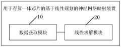
第二方面,提供一种用于存算一体芯片的基于线性规划的神经网络映射装置,包括:In a second aspect, a linear programming-based neural network mapping device for a memory-computing integrated chip is provided, including:
数据获取模块,获取待映射神经网络各层的权重阵列以及对应的偏置阵列数据、目标存算一体芯片的硬件参数;The data acquisition module acquires the weight array of each layer of the neural network to be mapped, the corresponding bias array data, and the hardware parameters of the target memory-computing integrated chip;
线性求解模块,将该待映射神经网络各层的权重阵列以及对应的偏置阵列数据、目标存算一体芯片的硬件参数输入预建立的线性规划求解模型进行求解得到映射方案,该映射方案用于将该待映射神经网络各层的权重阵列以及对应的偏置阵列映射至该目标存算一体芯片中。The linear solving module is used to input the weight array of each layer of the neural network to be mapped, the corresponding bias array data, and the hardware parameters of the target memory-computing integrated chip into a pre-established linear programming model for solving to obtain a mapping scheme. The mapping scheme is used for The weight array and the corresponding bias array of each layer of the neural network to be mapped are mapped to the target storage-computing integrated chip.
第三方面,提供一种存算一体芯片,包括:用于执行神经网络运算的闪存单元阵列,该闪存单元阵列中映射有该神经网络的权重阵列和偏置阵列;In a third aspect, a memory-computing integrated chip is provided, including: a flash memory cell array for performing neural network operations, and the weight array and bias array of the neural network are mapped in the flash memory cell array;
该权重阵列以及对应的偏置阵列的排布方式根据上述的基于线性规划的神经网络映射方法产生。The arrangement of the weight array and the corresponding bias array is generated according to the above-mentioned neural network mapping method based on linear programming.
第四方面,提供一种电子设备,包括存储器、处理器及存储在存储器上并可在处理器上运行的计算机程序,该处理器执行该程序时实现上述的基于线性规划的神经网络映射方法的步骤。In a fourth aspect, an electronic device is provided, comprising a memory, a processor and a computer program stored in the memory and running on the processor, when the processor executes the program, the above-mentioned linear programming-based neural network mapping method is realized. step.
第五方面,提供一种计算机可读存储介质,其上存储有计算机程序,该计算机程序被处理器执行时实现上述的基于线性规划的神经网络映射方法的步骤。In a fifth aspect, a computer-readable storage medium is provided, on which a computer program is stored, and when the computer program is executed by a processor, implements the steps of the above-mentioned linear programming-based neural network mapping method.
本发明实施例提供了一种用于存算一体芯片的基于线性规划的神经网络映射方法、装置、存算一体芯片、电子设备以及计算机可读存储介质,该方法包括:获取待映射神经网络各层的权重阵列以及对应的偏置阵列数据、目标存算一体芯片的硬件参数;将该待映射神经网络各层的权重阵列以及对应的偏置阵列数据、目标存算一体芯片的硬件参数输入预建立的线性规划求解模型进行求解得到映射方案,该映射方案用于将该待映射神经网络各层的权重阵列以及对应的偏置阵列映射至该目标存算一体芯片中。其中,通过将基于直观经验的权重和偏置数据映射过程转换为线性规划的数学模型的求解问题,提高运算精度。Embodiments of the present invention provide a linear programming-based neural network mapping method and device for a memory-computing integrated chip, an integrated memory-computing chip, an electronic device, and a computer-readable storage medium. The method includes: acquiring each neural network to be mapped Layer weight array and corresponding bias array data, hardware parameters of the target memory-computing integrated chip; input the weight array of each layer of the neural network to be mapped, the corresponding bias array data, and the hardware parameters of the target memory-computing integrated chip into the pre- The established linear programming solution model is solved to obtain a mapping scheme, and the mapping scheme is used to map the weight array and the corresponding bias array of each layer of the neural network to be mapped to the target memory-computing integrated chip. Among them, the calculation accuracy is improved by converting the weight and bias data mapping process based on intuitive experience into a linear programming mathematical model solving problem.
另外,本发明实施例中将偏置最小行数和偏置阵列的限制作为求解器的约束,对各偏置占据的行数进行了扩展,减少单个闪存单元上的存放的偏置的数值大小,降低电流噪声,进一步提高了运算精度。In addition, in the embodiment of the present invention, the limit of the minimum number of offset rows and the offset array is used as the constraints of the solver, and the number of rows occupied by each offset is expanded to reduce the numerical size of the offset stored on a single flash memory unit. , reduce the current noise, and further improve the operation accuracy.
为让本发明的上述和其他目的、特征和优点能更明显易懂,下文特举较佳实施例,并配合所附图式,作详细说明如下。In order to make the above-mentioned and other objects, features and advantages of the present invention more obvious and easy to understand, the preferred embodiments are exemplified below, and are described in detail as follows in conjunction with the accompanying drawings.
附图说明Description of drawings
为了更清楚地说明本申请实施例或现有技术中的技术方案,下面将对实施例或现有技术描述中所需要使用的附图作简单地介绍,显而易见地,下面描述中的附图是本申请的一些实施例,对于本领域普通技术人员来讲,在不付出创造性劳动的前提下,还可以根据这些附图获得其他的附图。在附图中:In order to more clearly illustrate the embodiments of the present application or the technical solutions in the prior art, the following briefly introduces the accompanying drawings that need to be used in the description of the embodiments or the prior art. Obviously, the drawings in the following description are For some embodiments of the present application, for those of ordinary skill in the art, other drawings can also be obtained according to these drawings without any creative effort. In the attached image:
图1示出了本发明实施例中的用于存算一体芯片的基于线性规划的神经网络映射方法的流程图;FIG. 1 shows a flowchart of a linear programming-based neural network mapping method for a memory-computing integrated chip in an embodiment of the present invention;
图2例举了本发明实施例中的闪存单元阵列划分方式;FIG. 2 illustrates a division method of a flash memory cell array in an embodiment of the present invention;
图3示出了本发明实施例中的闪存单元阵列的参数详情;FIG. 3 shows parameter details of the flash memory cell array in the embodiment of the present invention;
图4例举了本发明实施例中的权重矩阵以及对应的Bias的排布结果;Fig. 4 illustrates the weight matrix in the embodiment of the present invention and the arrangement result of the corresponding Bias;
图5是本发明实施例中的用于存算一体芯片的基于线性规划的神经网络映射装置的结构框图;5 is a structural block diagram of a linear programming-based neural network mapping device for a memory-computing integrated chip in an embodiment of the present invention;
图6为本发明实施例电子设备的结构图。FIG. 6 is a structural diagram of an electronic device according to an embodiment of the present invention.
具体实施方式Detailed ways
为了使本技术领域的人员更好地理解本申请方案,下面将结合本申请实施例中的附图,对本申请实施例中的技术方案进行清楚、完整地描述,显然,所描述的实施例仅仅是本申请一部分的实施例,而不是全部的实施例。基于本申请中的实施例,本领域普通技术人员在没有做出创造性劳动前提下所获得的所有其他实施例,都应当属于本申请保护的范围。In order to make those skilled in the art better understand the solutions of the present application, the technical solutions in the embodiments of the present application will be clearly and completely described below with reference to the accompanying drawings in the embodiments of the present application. Obviously, the described embodiments are only The embodiments are part of the present application, but not all of the embodiments. Based on the embodiments in the present application, all other embodiments obtained by those of ordinary skill in the art without creative work shall fall within the scope of protection of the present application.
本领域内的技术人员应明白,本发明的实施例可提供为方法、系统、或计算机程序产品。因此,本发明可采用完全硬件实施例、完全软件实施例、或结合软件和硬件方面的实施例的形式。而且,本发明可采用在一个或多个其中包含有计算机可用程序代码的计算机可用存储介质(包括但不限于磁盘存储器、CD-ROM、光学存储器等)上实施的计算机程序产品的形式。As will be appreciated by one skilled in the art, embodiments of the present invention may be provided as a method, system, or computer program product. Accordingly, the present invention may take the form of an entirely hardware embodiment, an entirely software embodiment, or an embodiment combining software and hardware aspects. Furthermore, the present invention may take the form of a computer program product embodied on one or more computer-usable storage media (including, but not limited to, disk storage, CD-ROM, optical storage, etc.) having computer-usable program code embodied therein.
需要说明的是,本申请的说明书和权利要求书及上述附图中的术语“包括”和“具有”以及他们的任何变形,意图在于覆盖不排他的包含,例如,包含了一系列步骤或单元的过程、方法、系统、产品或设备不必限于清楚地列出的那些步骤或单元,而是可包括没有清楚地列出的或对于这些过程、方法、产品或设备固有的其它步骤或单元。It should be noted that the terms "comprising" and "having" in the description and claims of the present application and the above-mentioned drawings, as well as any modifications thereof, are intended to cover non-exclusive inclusion, for example, including a series of steps or units The processes, methods, systems, products or devices are not necessarily limited to those steps or units expressly listed, but may include other steps or units not expressly listed or inherent to such processes, methods, products or devices.
需要说明的是,在不冲突的情况下,本申请中的实施例及实施例中的特征可以相互组合。下面将参考附图并结合实施例来详细说明本申请。It should be noted that the embodiments in the present application and the features of the embodiments may be combined with each other in the case of no conflict. The present application will be described in detail below with reference to the accompanying drawings and in conjunction with the embodiments.
图1示出了本发明实施例中的用于存算一体芯片的基于线性规划的神经网络映射方法的流程图;如图1所示,该用于存算一体芯片的基于线性规划的神经网络映射方法可以包括以下内容:FIG. 1 shows a flowchart of a linear programming-based neural network mapping method for a memory-computing integrated chip in an embodiment of the present invention; as shown in FIG. 1 , the linear programming-based neural network for a memory-computing integrated chip Mapping methods can include the following:
步骤S100:获取待映射神经网络各层的权重阵列以及对应的偏置阵列数据、目标存算一体芯片的硬件参数;Step S100: obtaining the weight array of each layer of the neural network to be mapped, the corresponding bias array data, and the hardware parameters of the target memory-computing integrated chip;
其中,所述各层的权重阵列以及对应的偏置阵列数据包括:各层权重阵列的行数和列数、对应的偏置最小行数;Wherein, the weight array of each layer and the corresponding offset array data include: the number of rows and columns of the weight array of each layer, and the corresponding minimum offset row number;
所述目标一体芯片的硬件参数包括:用于写入权重阵列的闪存单元阵列的行最大值和列最大值、用于写入偏置的闪存单元阵列的行最大值、最大运算块的行数和最小运算块的列数。The hardware parameters of the target integrated chip include: the row maximum value and the column maximum value of the flash memory cell array used for writing the weight array, the row maximum value of the flash memory cell array used for writing the bias, and the maximum number of rows of the operation block. and the number of columns of the minimum operation block.
值得说明的是,目标一体芯片的闪存单元阵列在硬件设计阶段已经设计出用于写入权重阵列的闪存单元阵列以及用于写入偏置的闪存单元阵列;针对已经训练好的特定神经网络,各层的权重矩阵参数以及Bias参数、Bias大小与在芯片上占据的最少行数、目标存算一体芯片的硬件参数为已知。It is worth noting that the flash memory cell array of the target integrated chip has been designed in the hardware design stage for the flash memory cell array for writing the weight array and the flash memory cell array for writing the bias; for the specific neural network that has been trained, The weight matrix parameters and Bias parameters of each layer, the Bias size and the minimum number of rows occupied on the chip, and the hardware parameters of the target memory-computing integrated chip are known.
步骤S200:将所述待映射神经网络各层的权重阵列以及对应的偏置阵列数据、目标存算一体芯片的硬件参数输入预建立的线性规划求解模型进行求解得到映射方案,所述映射方案用于将所述待映射神经网络各层的权重阵列以及对应的偏置阵列映射至所述目标存算一体芯片中。Step S200: Input the weight array of each layer of the neural network to be mapped, the corresponding bias array data, and the hardware parameters of the target memory-computing integrated chip into a pre-established linear programming solution model to solve to obtain a mapping scheme. The weight array of each layer of the neural network to be mapped and the corresponding bias array are mapped to the target memory-computing integrated chip.
其中,求解器是预建立的线性规划模型,实际应用中,可以直接在Python等中调用开源线性规划求解器,举例来说,可以采用谷歌的开源线性规划求解器。Among them, the solver is a pre-established linear programming model. In practical applications, the open-source linear programming solver can be called directly in Python, for example, Google's open-source linear programming solver can be used.
本发明实施例,通过把基于经验的权重和Bias映射问题,经过恰当的数学建模,转换为线性规划的求解问题,为网络权重和Bias的映射,以及Bias扩展提供严格的数学基础,寻找最佳排布结果,可以获得理论上的最优解,方案便于扩展,方便增加和减少映射中的限制,同等兼顾了权重和Bias映射以及Bias扩展,降低电流噪声,提高了运算精度。In the embodiment of the present invention, by transforming the empirical-based weight and Bias mapping problem into a linear programming solution problem through proper mathematical modeling, a strict mathematical basis is provided for the mapping of network weights and Bias, and Bias expansion, and finds the best solution. The optimal arrangement results can obtain the theoretical optimal solution. The scheme is easy to expand, and it is convenient to increase and decrease the restrictions in the mapping. It also takes into account the weight and Bias mapping and Bias expansion, reduces the current noise, and improves the operation accuracy.
值得说明的是,由于存算一体芯片计算的特殊性,权重矩阵与其对应的Bias需要列对齐,因此,Bias的排布位置与对应的权重矩阵的排布位置列对齐,行方向的排布方式依据Bias最小行数进行排布。It is worth noting that due to the particularity of the calculation of the integrated storage and computing chip, the weight matrix and its corresponding Bias need to be aligned in columns. Therefore, the layout position of the Bias is aligned with the layout position of the corresponding weight matrix, and the layout method in the row direction Arrange according to the minimum number of lines in Bias.
通过上述步骤S100、步骤S200产生排布方案,后续根据排布方案将神经网络各层参数通过编译工具写入存算一体芯片的闪存单元阵列中,在应用推理阶段,根据排布方案,结合控制需求,在执行某一层神经网络运算时,通过行列译码器,选通该层神经网络运算对应权重矩阵和Bias所在行列,将该层神经网络的输入信号输入权重矩阵对应的行,与权重矩阵进行矩阵乘加运算,而后与对应的Bias叠加,在对应列获得该层神经网络的计算结果。The arrangement scheme is generated through the above steps S100 and S200, and then according to the arrangement scheme, the parameters of each layer of the neural network are written into the flash memory cell array of the integrated memory-computing chip through the compilation tool. In the application reasoning stage, according to the arrangement scheme, combined with the control Requirement, when performing a certain layer of neural network operation, through the row and column decoder, select the weight matrix corresponding to the layer of neural network operation and the row and column where Bias is located, input the input signal of this layer of neural network into the row corresponding to the weight matrix, and the weight matrix. The matrix is multiplied and added by the matrix, and then superimposed with the corresponding Bias, and the calculation result of the neural network of this layer is obtained in the corresponding column.
图2例举了本发明实施例中的闪存单元阵列划分方式,如图2中的(a)所示,芯片的实际物理架构由主阵列(用于写入权重阵列)和Bias(偏置)阵列组成。在实际应用过程中,由于模拟计算过程中电流太大会对计算结果造成显著影响,因此,存算一体芯片在设计时会给出一个最大运算块,即单次运算的最大规模,如果运算规模超过最大运算块,可需要分多次进行运算,如图2中的(b)所示,主阵列可以被分成2×4块,这里的划分是根据芯片的实际性能进行的,且可以划分的每一块大小相同,也可以划分的每一块大小不同,本发明实施例对此不做限制。另外,为了保障工作效率,存算一体芯片在设计时会给出一个最小运算块,即单次运算的最小规模,防止在应用阶段,单次运算量过小导致的效率降低。FIG. 2 illustrates the division method of the flash memory cell array in the embodiment of the present invention. As shown in (a) of FIG. 2 , the actual physical structure of the chip consists of the main array (for writing the weight array) and the Bias (bias) array composition. In the actual application process, since the current is too large in the simulation calculation process, the calculation results will be significantly affected. Therefore, the memory-computing integrated chip will be designed with a maximum operation block, that is, the maximum scale of a single operation. If the operation scale exceeds The largest operation block may need to be operated in multiple times. As shown in (b) in Figure 2, the main array can be divided into 2 × 4 blocks. The division here is based on the actual performance of the chip, and each can be divided. A block has the same size, and each block that can be divided has a different size, which is not limited in this embodiment of the present invention. In addition, in order to ensure work efficiency, the integrated memory and computing chip will be designed with a minimum operation block, that is, the minimum size of a single operation, to prevent the efficiency reduction caused by too small a single operation in the application stage.
在一个可选的实施例中,该用于存算一体芯片的基于线性规划的神经网络映射方法还可以包括:根据映射方案将所述待映射神经网络各层的权重矩阵和Bias写入所述存算一体芯片上。In an optional embodiment, the linear programming-based neural network mapping method for a memory-computing integrated chip may further include: writing the weight matrix and Bias of each layer of the neural network to be mapped into the Stored on the integrated chip.
具体地,上述的映射方法是在工具链上执行的,可以理解为运行在终端设备或服务器或芯片烧录装置上的程序,通过上述映射方法产生排布方案,而后还需要根据该排布方案将权重矩阵和Bias写入所述存算一体芯片上。而后存算一体芯片就可以安装到对应的设备电路板上,进行推理应用,实现神经网络运算,比如可以安装在玩具上进行语音识别,此时,芯片中写入的神经网络参数是语音识别神经网络对应的参数;当然,该存算一体芯片也可以是安装在人脸识别设备上,该芯片中写入的神经网络参数是图像识别神经网络对应的参数,当然,上述只是例举了几种芯片应用场景,本发明实施例对芯片的应用场景不做限制,可以是需要进行神经网络运算的各种设备和场景。Specifically, the above-mentioned mapping method is executed on the tool chain, which can be understood as a program running on a terminal device, a server or a chip burning device, and an arrangement scheme is generated through the above-mentioned mapping method, and then it needs to be based on the arrangement scheme. Write the weight matrix and Bias on the memory-computing integrated chip. Then the integrated storage and computing chip can be installed on the corresponding device circuit board to perform reasoning applications and realize neural network operations. For example, it can be installed on toys for speech recognition. At this time, the neural network parameters written in the chip are speech recognition neural networks. The parameters corresponding to the network; of course, the integrated storage and computing chip can also be installed on the face recognition device. The neural network parameters written in the chip are the parameters corresponding to the image recognition neural network. Of course, the above are just examples of several Chip application scenario, the embodiment of the present invention does not limit the application scenario of the chip, which may be various devices and scenarios that need to perform neural network operations.
图3示出了本发明实施例中的闪存单元阵列的参数详情;参见图3,第i层权重阵列的行数为rows[i]、第i层权重阵列的列数为cols[i]、对应的偏置最小行数为bias[i];Fig. 3 shows the parameter details of the flash memory cell array in the embodiment of the present invention; referring to Fig. 3, the row number of the i-th layer weight array is rows[i], the column number of the i-th layer weight array is cols[i], The corresponding bias minimum number of rows is bias[i];
目标一体芯片的硬件参数中,用于写入权重阵列的闪存单元阵列的行最大值为row_size,列最大值为col_size、用于写入偏置的闪存单元阵列的行最大值为bias_size。模型输出为:x[i],y[i],bx[i],by[i],bias[i],其中,x[i]为第i层权重阵列在用于写入权重阵列的闪存单元阵列中的行起始地址,y[i]为第i层权重阵列在用于写入权重阵列的闪存单元阵列中的列起始地址,bx[i]为第i层偏置在用于写入偏置的闪存单元阵列中的行起始地址,by[i]为第i层偏置在用于写入偏置的闪存单元阵列中的列起始地址,bias[i]为经过扩展排布后第i层偏置在用于写入偏置的闪存单元阵列中的行数;最大运算块的行数为P,举例来说,假设一存内计算芯片固设的最大运算块的规模时512*128,即单次运算最大的规模,此时,P=512;In the hardware parameters of the target integrated chip, the maximum row value of the flash cell array used for writing the weight array is row_size, the maximum column value is col_size, and the maximum row value of the flash cell array used for writing bias is bias_size. The model output is: x[i], y[i], bx[i], by[i], bias[i], where x[i] is the weight array of the i-th layer in the flash memory used to write the weight array The row start address in the cell array, y[i] is the column start address of the i-th layer weight array in the flash cell array used to write the weight array, and bx[i] is the i-th layer offset in the flash memory cell array used for writing the weight array. The row start address in the write-biased flash memory cell array, by[i] is the column start address of the i-th layer biased in the write-biased flash memory cell array, and bias[i] is the extended The number of rows of the i-th layer biased in the flash memory cell array used for writing bias after arrangement; the row number of the maximum operation block is P, for example, assuming that the maximum operation block fixed in an in-memory computing chip is The scale is 512*128, which is the largest scale of a single operation. At this time, P=512;
在一个可选的实施例中,该线性规划求解模型的约束条件包括:In an optional embodiment, the constraints of the linear programming solution model include:
1、各层权重的行起始地址位于0和用于写入权重阵列的闪存单元阵列的行最大值之间;即:0≤x[i]≤rowsize-rows[i]);1. The row start address of each layer of weight is located between 0 and the row maximum value of the flash cell array used to write the weight array; namely: 0≤x[i]≤rowsize-rows[i]);
2、各层权重的列起始地址位于0和用于写入权重阵列的闪存单元阵列的列最大值之间;即:0≤y[i]≤colsize-cals[i];2. The column start address of each layer of weight is located between 0 and the column maximum value of the flash cell array used to write the weight array; namely: 0≤y[i]≤colsize-cals[i];
3、各层偏置的行起始地址位于0和用于写入偏置的闪存单元阵列的行最大值之间;即:(0≤bx[i]≤biassize-bias[i]);3. The row start address of each layer bias is located between 0 and the row maximum value of the flash memory cell array used for the write bias; namely: (0≤bx[i]≤biassize-bias[i]);
4、各层偏置的列起始地址与对应层的权重的列起始地址相等;即:by[i]=y[i];4. The column start address of the offset of each layer is equal to the column start address of the weight of the corresponding layer; namely: by[i]=y[i];
5、各层权重的排布,两两之间互相不重叠;即:x[i]≥x[j]+rows[j]or x[j]≥x[i]+rows[i]or y[i]≥y[j]+cols[j]or y[j]≥y[i]+cols[i];5. The weights of each layer are arranged so that they do not overlap each other; namely: x[i]≥x[j]+rows[j]or x[j]≥x[i]+rows[i]or y [i]≥y[j]+cols[j]or y[j]≥y[i]+cols[i];
6、各层偏置的排布,两两之间互相不重叠。即:bx[i]≥bx[j]+bias[j]or bx[j]≥bx[i]+bias[i];6. The offset arrangement of each layer does not overlap with each other. That is: bx[i]≥bx[j]+bias[j] or bx[j]≥bx[i]+bias[i];
线性规划求解模型的目标函数包括:The objective function of the linear programming solver model includes:
1、各层偏置的排布行数位于各层偏置最小行数与所述用于写入偏置的闪存单元阵列的行最大值之间,且所有层的偏置的排布行数总和最大,即:(max∑bias[i]);1. The number of rows for the offset of each layer is located between the minimum number of rows for the offset of each layer and the maximum row value of the flash memory cell array used for write bias, and the number of rows for the offset of all layers is arranged The maximum sum is: (max∑bias[i]);
2、将用于写入权重阵列的闪存单元阵列按纵向均分成Y个区,各区的宽度均为X列,排布后各层权重所跨越的分区之和最小,即min∑across[i],

通过采用上述技术方案,优化了约束条件和求解目标,基于上述约束条件和求解目标进行线性求解后,能够得到神经网络模型权重矩阵和偏置矩阵的最优排布。By adopting the above technical solution, the constraints and the solution objectives are optimized, and after linear solution is performed based on the above constraints and solution objectives, the optimal arrangement of the weight matrix and the bias matrix of the neural network model can be obtained.
在一个可选的实施例中,还可以支持权重阵列和Bias阵列空间余量,预留前M行、后N行、前J列以及后K列预留空间(将第1、2条的0和最大值基于这一限制相应更改即可);In an optional embodiment, the space margin of the weight array and the Bias array can also be supported, and the reserved space of the first M rows, the last N rows, the first J columns, and the last K columns is reserved (the 0 of the first and second columns are reserved. and the maximum value can be changed accordingly based on this limit);
线性规划求解模型的约束条件包括:The constraints of the linear programming solver model include:
1、各层权重的行起始地址位于M和用于写入权重阵列的闪存单元阵列的行最大值减去对应层权重阵列的行数再减去N的差值之间;即M≤x[i]≤rawsize-rows[i]-N;1. The row start address of each layer weight is located between M and the maximum value of the row of the flash cell array used to write the weight array minus the number of rows in the corresponding layer weight array minus N; that is, M≤x [i]≤rawsize-rows[i]-N;
2、各层权重的列起始地址位于J和用于写入权重阵列的闪存单元阵列的列最大值减去对应层权重阵列的行数再减去K的差值之间;即:J≤y[i]≤colsize-cals[i]-K;2. The column start address of each layer weight is located between J and the difference between the maximum column value of the flash memory cell array used to write the weight array minus the row number of the corresponding layer weight array and then minus K; that is: J≤ y[i]≤colsize-cals[i]-K;
3、各层偏置的行起始地址位于0和用于写入偏置的闪存单元阵列的行最大值之间;即:(0≤bx[i]≤biassize-bias[i])3. The row start address of each layer bias is located between 0 and the row maximum value of the flash cell array used for the write bias; namely: (0≤bx[i]≤biassize-bias[i])
4、各层偏置的列起始地址与对应层的权重的列起始地址相等;即:by[i]=y[i];4. The column start address of the offset of each layer is equal to the column start address of the weight of the corresponding layer; namely: by[i]=y[i];
5、各层权重的排布,两两之间互相不重叠;即:x[i]≥x[j]+rows[j]or x[j]≥x[i]+rows[i]or y[i]≥y[j]+cols[j]or y[j]≥y[i]+cols[i];5. The weights of each layer are arranged so that they do not overlap each other; namely: x[i]≥x[j]+rows[j]or x[j]≥x[i]+rows[i]or y [i]≥y[j]+cols[j]or y[j]≥y[i]+cols[i];
6、各层偏置的排布,两两之间互相不重叠。即:bx[i]≥bx[j]+bias[j]or bx[j]≥bx[i]+bias[i];6. The offset arrangement of each layer does not overlap with each other. That is: bx[i]≥bx[j]+bias[j] or bx[j]≥bx[i]+bias[i];
线性规划求解模型的目标函数包括:The objective function of the linear programming solver model includes:
1、各层偏置的排布行数位于各层偏置最小行数与所述用于写入偏置的闪存单元阵列的行最大值之间,且所有层的偏置的排布行数总和最大,即:(max∑bias[i]);1. The number of rows for the offset of each layer is located between the minimum number of rows for the offset of each layer and the maximum row value of the flash memory cell array used for write bias, and the number of rows for the offset of all layers is arranged The maximum sum is: (max∑bias[i]);
2、将用于写入权重阵列的闪存单元阵列按纵向均分成Y个区,各区的宽度均为X列,排布后各层权重所跨越的分区之和最小,即min∑across[i],

在一个可选的实施例中,线性规划求解模型的约束条件还包括:根据用于写入权重阵列的闪存单元阵列的行最大值以及最大运算块的行数将用于写入权重阵列的闪存单元阵列均分成多层,各层权重的行起始地址和行结束地址不能跨层。In an optional embodiment, the constraints of the linear programming solution model further include: according to the maximum row value of the flash memory cell array used for writing the weight array and the row number of the maximum operation block, the flash memory used for writing the weight array will be used for writing the weight array. The cell array is divided into multiple layers, and the row start address and row end address of the weight of each layer cannot cross layers.
具体地,线性规划求解模型的约束条件包括:Specifically, the constraints of the linear programming solution model include:
1、各层权重的行起始地址位于0和用于写入权重阵列的闪存单元阵列的行最大值之间;即:0≤x[i]≤rowsize-rows[i]);1. The row start address of each layer of weight is located between 0 and the row maximum value of the flash cell array used to write the weight array; namely: 0≤x[i]≤rowsize-rows[i]);
2、各层权重的列起始地址位于0和用于写入权重阵列的闪存单元阵列的列最大值之间;即:0≤y[i]≤colsize-cols[i];2. The column start address of each layer of weight is located between 0 and the column maximum value of the flash cell array used for writing the weight array; namely: 0≤y[i]≤colsize-cols[i];
3、各层偏置的行起始地址位于0和用于写入偏置的闪存单元阵列的行最大值之间;即:(0≤bx[i]≤biassize-bias[i]);3. The row start address of each layer bias is located between 0 and the row maximum value of the flash memory cell array used for the write bias; namely: (0≤bx[i]≤biassize-bias[i]);
4、各层偏置的列起始地址与对应层的权重的列起始地址相等;即:by[i]=y[i];4. The column start address of the offset of each layer is equal to the column start address of the weight of the corresponding layer; namely: by[i]=y[i];
5、各层权重的排布,两两之间互相不重叠;即:x[i]≥x[j]+rows[j]or x[j]≥x[i]+rows[i]or y[i]≥y[j]+cols[j]or y[j]≥y[i]+cols[i];5. The weights of each layer are arranged so that they do not overlap each other; namely: x[i]≥x[j]+rows[j]or x[j]≥x[i]+rows[i]or y [i]≥y[j]+cols[j]or y[j]≥y[i]+cols[i];
6、各层偏置的排布,两两之间互相不重叠。即:bx[i]≥bx[j]+bias[j]or bx[j]≥bx[i]+bias[i];6. The offset arrangement of each layer does not overlap with each other. That is: bx[i]≥bx[j]+bias[j] or bx[j]≥bx[i]+bias[i];
7、权重阵列按P对齐均分成Q层,各层权重的行起始地址和行结束地址不能跨层(如将行均分为Q层时,限制是


即:将用于写入权重阵列的闪存单元阵列按P对齐均分成Q层;其中,所述P为最大运算块的行数;所述Q为用于写入权重阵列的闪存单元阵列的行最大值除以P后取整。Q=row_size/P,例如对于row_size=1024,P=512时,Q=1024/512=2,即均分为两层。That is, the flash memory cell array used for writing the weight array is divided into Q layers according to the alignment of P; wherein, the P is the number of rows of the largest operation block; the Q is the row of the flash memory cell array used for writing the weight array The maximum value is divided by P and rounded up. Q=row_size/P, for example, when row_size=1024 and P=512, Q=1024/512=2, that is, it is equally divided into two layers.
举例来说,当前的闪存单元阵列的行最大值,分别为1792和2048,都是被分成了2层,每层行数为896和1024,权重分配的时候不能跨层,权重分配可以跨448/512,但不能够跨896/1024,其中,448和512是最大运算块的行数,即:把闪存单元阵列按横向分成4层,每层有448/512行,权重分配的时候1、2层,3、4层可以跨,尽量少跨,禁止跨2、3层。For example, the current maximum row values of the flash memory cell array are 1792 and 2048, which are divided into 2 layers, and the number of rows in each layer is 896 and 1024. When assigning weights, you cannot cross layers, but you can assign weights across 448. /512, but cannot span 896/1024, where 448 and 512 are the rows of the largest operation block, that is, the flash memory cell array is divided into 4 layers horizontally, each layer has 448/512 rows, when the weight is allocated 1, The 2nd, 3rd, and 4th floors can be crossed, but as little as possible, and the 2nd and 3rd floors are prohibited.
线性规划求解模型的目标函数包括:The objective function of the linear programming solver model includes:
1、各层偏置的排布行数位于各层偏置最小行数与所述用于写入偏置的闪存单元阵列的行最大值之间,且所有层的偏置的排布行数总和最大,即:(max∑bias[i]);1. The number of rows for the offset of each layer is located between the minimum number of rows for the offset of each layer and the maximum row value of the flash memory cell array used for write bias, and the number of rows for the offset of all layers is arranged The maximum sum is: (max∑bias[i]);
2、将用于写入权重阵列的闪存单元阵列按纵向均分成Y个区,各区的宽度均为X列,排布后各层权重所跨越的分区之和最小,即min∑across[i],

通过采用上述技术方案,能够进一步提高运算精度。By adopting the above technical solution, the operation accuracy can be further improved.
在一个可选的实施例中,线性规划求解模型的约束条件包括:In an optional embodiment, the constraints of the linear programming solution model include:
1、各层权重的行起始地址位于0和用于写入权重阵列的闪存单元阵列的行最大值之间;即:0≤x[i]≤rowsize-rows[i]);1. The row start address of each layer of weight is located between 0 and the row maximum value of the flash cell array used to write the weight array; namely: 0≤x[i]≤rowsize-rows[i]);
2、各层权重的列起始地址位于0和用于写入权重阵列的闪存单元阵列的列最大值之间;即:0≤y[i]≤colsize-cols[i];2. The column start address of each layer of weight is located between 0 and the column maximum value of the flash cell array used for writing the weight array; namely: 0≤y[i]≤colsize-cols[i];
3、各层偏置的行起始地址位于0和用于写入偏置的闪存单元阵列的行最大值之间;即:(0≤bx[i]≤biassize-bias[i]);3. The row start address of each layer bias is located between 0 and the row maximum value of the flash memory cell array used for the write bias; namely: (0≤bx[i]≤biassize-bias[i]);
4、各层偏置的列起始地址与对应层的权重的列起始地址相等;即:by[i]=y[i];4. The column start address of the offset of each layer is equal to the column start address of the weight of the corresponding layer; namely: by[i]=y[i];
5、各层权重的排布,两两之间互相不重叠;即:x[i]≥x[j]+rows[j]or x[j]≥x[i]+rows[i]or y[i]≥y[j]+cols[j]or y[j]≥y[i]+cols[i];5. The weights of each layer are arranged so that they do not overlap each other; namely: x[i]≥x[j]+rows[j]or x[j]≥x[i]+rows[i]or y [i]≥y[j]+cols[j]or y[j]≥y[i]+cols[i];
6、各层偏置的排布,两两之间互相不重叠。即:bx[i]≥bx[j]+bias[j]or bx[j]≥bx[i]+bias[i];6. The offset arrangement of each layer does not overlap with each other. That is: bx[i]≥bx[j]+bias[j] or bx[j]≥bx[i]+bias[i];
7、权重阵列按P对齐均分成Q层,各层权重的行起始地址和行结束地址不能跨层(如将行均分为Q层时,限制是


即:将用于写入权重阵列的闪存单元阵列按P对齐均分成Q层;其中,所述P为最大运算块的行数;所述Q为用于写入权重阵列的闪存单元阵列的行最大值除以P后取整。Q=row_size/P,例如对于row_size=1024,P=512时,Q=1024/512=2,即均分为两层。That is, the flash memory cell array used for writing the weight array is divided into Q layers according to the alignment of P; wherein, the P is the number of rows of the largest operation block; the Q is the row of the flash memory cell array used for writing the weight array The maximum value is divided by P and rounded up. Q=row_size/P, for example, when row_size=1024 and P=512, Q=1024/512=2, that is, it is equally divided into two layers.
8、各层偏置的排布行数为偶数;即:各层Bias扩充的行数,必须为偶数(bias[i]mod 2=0)8. The number of rows for the bias arrangement of each layer is an even number; that is, the number of rows for Bias expansion of each layer must be an even number (bias[i]
线性规划求解模型的目标函数包括:The objective function of the linear programming solver model includes:
1、各层偏置的排布行数位于各层偏置最小行数与所述用于写入偏置的闪存单元阵列的行最大值之间,且所有层的偏置的排布行数总和最大,即:(max∑bias[i]);1. The number of rows for the offset of each layer is located between the minimum number of rows for the offset of each layer and the maximum row value of the flash memory cell array used for write bias, and the number of rows for the offset of all layers is arranged The maximum sum is: (max∑bias[i]);
2、将用于写入权重阵列的闪存单元阵列按纵向均分成Y个区,各区的宽度均为X列,排布后各层权重所跨越的分区之和最小,即min∑across[i],

通过采用上述技术方案,对各偏置占据的行数进行了扩展,减少单个闪存单元上的存放的偏置的数值大小,降低电流噪声,进一步提高了运算精度。By adopting the above technical solution, the number of rows occupied by each bias is expanded, the numerical value of the bias stored in a single flash memory unit is reduced, the current noise is reduced, and the operation precision is further improved.
值得说明的是,神经网络模型确定之后,知道了各层的权重阵列以及偏置数值,根据偏置数值以及目标芯片的参数(每一行Bias的属性)计算出每一层的Bias最小行数。It is worth noting that after the neural network model is determined, the weight array and bias value of each layer are known, and the minimum number of Bias lines of each layer is calculated according to the bias value and the parameters of the target chip (the attributes of each line of Bias).
Bias的最小行数可以由电路方面的工程师根据精度要求事先给定,一般以满足最差精度要求为标准,也可以按照预设规则进行运算,本发明实施例对此不再赘述。The minimum number of rows of Bias may be predetermined by the circuit engineer according to the accuracy requirement, generally satisfying the worst accuracy requirement as the standard, or may be calculated according to preset rules, which will not be repeated in this embodiment of the present invention.
本发明实施例中,Bias排布的目标之一是Bias阵列的空闲行最少。为尽可能减少Bias阵列中全部或部分存算一体单元存储的Bias数值,需要利用Bias阵列中的空闲行对Bias的排布进行扩展,得到最终的排布方案,而后按照最终的排布方案将神经网络参数写入存算一体芯片中。In this embodiment of the present invention, one of the goals of Bias arrangement is to minimize the number of idle rows in the Bias array. In order to minimize the Bias value stored in all or part of the storage-computing integrated unit in the Bias array, it is necessary to use the free rows in the Bias array to expand the Bias arrangement to obtain the final arrangement scheme, and then according to the final arrangement scheme The neural network parameters are written into the integrated storage and computing chip.
由于存算一体芯片本质上采用模拟计算,Bias阵列上每个存算一体单元的bias值越大,最终计算产生的噪声就会越大,过大的Bias引入的过大噪声会对计算精度产生决定性影响,因此可以根据阵列大小,尽可能地扩展逻辑上一行Bias占据的实际Bias阵列行数,如占据的实际行数为m,则每一行上存放的Bias大小为逻辑上Bias大小的1/m,从而提高计算精度。Since the memory-computing integrated chip essentially uses analog computing, the larger the bias value of each memory-computing integrated unit on the Bias array, the greater the noise generated by the final calculation. Therefore, the actual number of Bias array rows occupied by a logical row of Bias can be expanded as much as possible according to the size of the array. If the actual number of rows occupied is m, the size of the Bias stored on each row is 1/ of the logical Bias size. m, so as to improve the calculation accuracy.
为了使本领域技术更好地理解本申请,下面举例对本发明实施例进行描述:假设目标存算一体芯片的硬件参数如表1所示,待映射神经网络模型的参数如表2所示。In order to better understand the present application for those skilled in the art, the following examples describe the embodiments of the present invention: it is assumed that the hardware parameters of the target memory-computing integrated chip are shown in Table 1, and the parameters of the neural network model to be mapped are shown in Table 2.
表1:目标存算一体芯片的硬件参数:Table 1: Hardware parameters of the target memory-computing integrated chip:


其中,单块权重阵列表示最大运算块,列对齐宽度表示最小运算块的列宽度;Among them, the single block weight array represents the largest operation block, and the column alignment width represents the column width of the smallest operation block;
表2:目标神经网络模型参数:Table 2: Target Neural Network Model Parameters:

其中,待映射神经网络模型有10个运算层,比如,若待映射神经网络为卷积神经网络CNN模型,则卷积层有10个;第1层神经网络的权重行数是440,列数/Bias的列数为112,第1层神经网络的最小Bias行数为2。Among them, the neural network model to be mapped has 10 operation layers. For example, if the neural network to be mapped is a convolutional neural network CNN model, there are 10 convolutional layers; the weight of the first layer of neural network is 440 rows and columns. The number of columns of /Bias is 112, and the minimum number of rows of Bias for layer 1 neural network is 2.
表3:映射方案Table 3: Mapping Scheme


表3示出了基于表1和表2的数据,利用本发明实施例中的用于存算一体芯片的基于线性规划的神经网络映射方法,得到的映射方案,将表3所示映射方案映射至目标神经网络之后的结果如图4所示。Table 3 shows the mapping scheme obtained based on the data in Table 1 and Table 2 by using the linear programming-based neural network mapping method for a memory-computing integrated chip in the embodiment of the present invention. The mapping scheme shown in Table 3 is mapped to The result after reaching the target neural network is shown in Figure 4.
其中,1~10层神经网络排布后的序号为0~9,举例来说,第1层神经网络排布后,其行起始地址x[0]=896,列起始地址y[0]=562;对应的Bias的行起始地址为bx[0]=0,列起始地址为by[0]=562;第1层神经网络最小Bias行数为2,扩展后的Bias行数为12行。Among them, the sequence numbers of 1-10 layers of neural networks are 0-9. For example, after the first layer of neural networks are arranged, the row start address x[0]=896, and the column start address y[0 ]=562; the row start address of the corresponding Bias is bx[0]=0, and the column start address is by[0]=562; the minimum number of Bias rows in the first layer of neural network is 2, and the number of expanded Bias rows for 12 lines.
本发明实施例还提供了一种存算一体芯片,包括:用于执行神经网络运算的闪存单元阵列,所述闪存单元阵列中映射有所述神经网络的权重阵列和偏置阵列;An embodiment of the present invention also provides an integrated memory and computing chip, including: a flash memory cell array for performing neural network operations, wherein the weight array and the bias array of the neural network are mapped in the flash memory cell array;
所述权重阵列以及对应的偏置阵列的排布方式根据上述的基于线性规划的神经网络映射方法产生。The arrangement of the weight array and the corresponding bias array is generated according to the above-mentioned neural network mapping method based on linear programming.
值得说明的是,本发明实施例提供的存算一体芯片,可以适用于各种电子设备,比如:智能手机、平板电子设备、网络机顶盒、便携式计算机、台式电脑、个人数字助理(PDA)、车载设备、智能穿戴设备、玩具、智能家居控制设备、流水线设备控制器等。其中,所述智能穿戴设备可以包括智能眼镜、智能手表、智能手环等。It is worth noting that the integrated storage and computing chip provided by the embodiment of the present invention can be applied to various electronic devices, such as: smart phones, tablet electronic devices, network set-top boxes, portable computers, desktop computers, personal digital assistants (PDA), vehicle-mounted Equipment, smart wearable devices, toys, smart home control equipment, assembly line equipment controllers, etc. Wherein, the smart wearable device may include smart glasses, smart watches, smart bracelets, and the like.
基于同一发明构思,本申请实施例还提供了一种用于存算一体芯片的基于线性规划的神经网络映射装置,可以用于实现上述实施例所描述的方法,如下面的实施例所述。由用于存算一体芯片的基于线性规划的神经网络映射装置解决问题的原理与上述方法相似,因此用于存算一体芯片的基于线性规划的神经网络映射装置的实施可以参见上述方法的实施,重复之处不再赘述。以下所使用的,术语“单元”或者“模块”可以实现预定功能的软件和/或硬件的组合。尽管以下实施例所描述的装置较佳地以软件来实现,但是硬件,或者软件和硬件的组合的实现也是可能并被构想的。Based on the same inventive concept, the embodiments of the present application also provide a linear programming-based neural network mapping device for a memory-computing integrated chip, which can be used to implement the methods described in the foregoing embodiments, as described in the following embodiments. The principle of solving the problem by the neural network mapping device based on linear programming for the integrated chip of storage and calculation is similar to the above method, so the implementation of the neural network mapping device based on linear programming for the integrated chip of storage and calculation can refer to the implementation of the above method, The repetition will not be repeated. As used below, the term "unit" or "module" may be a combination of software and/or hardware that implements a predetermined function. Although the apparatus described in the following embodiments is preferably implemented in software, implementations in hardware, or a combination of software and hardware, are also possible and contemplated.
图5是本发明实施例中的用于存算一体芯片的基于线性规划的神经网络映射装置的结构框图。该用于存算一体芯片的基于线性规划的神经网络映射装置包括:数据获取模块10、线性求解模块20。FIG. 5 is a structural block diagram of a linear programming-based neural network mapping device for a memory-computing integrated chip in an embodiment of the present invention. The linear programming-based neural network mapping device for a memory-computing integrated chip includes: a
数据获取模块10获取待映射神经网络各层的权重阵列以及对应的偏置阵列数据、目标存算一体芯片的硬件参数;The
线性求解模块20将所述待映射神经网络各层的权重阵列以及对应的偏置阵列数据、目标存算一体芯片的硬件参数输入预建立的线性规划求解模型进行求解得到映射方案,所述映射方案用于将所述待映射神经网络各层的权重阵列以及对应的偏置阵列映射至所述目标存算一体芯片中。The
上述实施例阐明的装置、模块或单元,具体可以由计算机芯片或实体实现,或者由具有某种功能的产品来实现。一种典型的实现设备为电子设备,具体的,电子设备例如可以为个人计算机、膝上型计算机、蜂窝电话、相机电话、智能电话、个人数字助理、媒体播放器、导航设备、电子邮件设备、游戏控制台、平板计算机、可穿戴设备或者这些设备中的任何设备的组合。The devices, modules or units described in the above embodiments may be specifically implemented by computer chips or entities, or by products with certain functions. A typical implementation device is an electronic device. Specifically, the electronic device can be, for example, a personal computer, a laptop computer, a cellular phone, a camera phone, a smart phone, a personal digital assistant, a media player, a navigation device, an email device, Game consoles, tablets, wearables, or a combination of any of these devices.
在一个典型的实例中电子设备具体包括存储器、处理器以及存储在存储器上并可在处理器上运行的计算机程序,所述处理器执行所述程序时实现上述的用于存算一体芯片的神经网络映射方法的步骤。In a typical example, the electronic device specifically includes a memory, a processor, and a computer program stored in the memory and running on the processor, when the processor executes the program, the above-mentioned neural network for a memory-computing integrated chip is implemented The steps of the network mapping method.
下面参考图6,其示出了适于用来实现本申请实施例的电子设备600的结构示意图。Referring next to FIG. 6 , it shows a schematic structural diagram of an electronic device 600 suitable for implementing the embodiments of the present application.
如图6所示,电子设备600包括中央处理单元(CPU)601,其可以根据存储在只读存储器(ROM)602中的程序或者从存储部分608加载到随机访问存储器(RAM))603中的程序而执行各种适当的工作和处理。在RAM603中,还存储有系统600操作所需的各种程序和数据。CPU601、ROM602、以及RAM603通过总线604彼此相连。输入/输出(I/O)接口605也连接至总线604。As shown in FIG. 6 , the electronic device 600 includes a central processing unit (CPU) 601 that can be loaded into a random access memory (RAM) 603 according to a program stored in a read only memory (ROM) 602 or from a
以下部件连接至I/O接口605:包括键盘、鼠标等的输入部分606;包括诸如阴极射线管(CRT)、液晶显示器(LCD)等以及扬声器等的输出部分607;包括硬盘等的存储部分608;以及包括诸如LAN卡,调制解调器等的网络接口卡的通信部分609。通信部分609经由诸如因特网的网络执行通信处理。驱动器610也根据需要连接至I/O接口605。可拆卸介质611,诸如磁盘、光盘、磁光盘、半导体存储器等等,根据需要安装在驱动器610上,以便于从其上读出的计算机程序根据需要被安装如存储部分608。The following components are connected to the I/O interface 605: an
特别地,根据本发明的实施例,上文参考流程图描述的过程可以被实现为计算机软件程序。例如,本发明的实施例包括一种计算机可读存储介质,其上存储有计算机程序,该计算机程序被处理器执行时实现上述的用于存算一体芯片的神经网络映射方法的步骤。In particular, the processes described above with reference to the flowcharts may be implemented as computer software programs according to embodiments of the present invention. For example, an embodiment of the present invention includes a computer-readable storage medium on which a computer program is stored, and when the computer program is executed by a processor, implements the steps of the above-mentioned neural network mapping method for a memory-computing integrated chip.
在这样的实施例中,该计算机程序可以通过通信部分609从网络上被下载和安装,和/或从可拆卸介质611被安装。In such an embodiment, the computer program may be downloaded and installed from the network via the
计算机可读介质包括永久性和非永久性、可移动和非可移动媒体可以由任何方法或技术来实现信息存储。信息可以是计算机可读指令、数据结构、程序的模块或其他数据。计算机的存储介质的例子包括,但不限于相变内存(PRAM)、静态随机存取存储器(SRAM)、动态随机存取存储器(DRAM)、其他类型的随机存取存储器(RAM)、只读存储器(ROM)、电可擦除可编程只读存储器(EEPROM)、快闪记忆体或其他内存技术、只读光盘只读存储器(CD-ROM)、数字多功能光盘(DVD)或其他光学存储、磁盒式磁带,磁带磁磁盘存储或其他磁性存储设备或任何其他非传输介质,可用于存储可以被计算设备访问的信息。按照本文中的界定,计算机可读介质不包括暂存电脑可读媒体(transitory media),如调制的数据信号和载波。Computer-readable media includes both persistent and non-permanent, removable and non-removable media, and storage of information may be implemented by any method or technology. Information may be computer readable instructions, data structures, modules of programs, or other data. Examples of computer storage media include, but are not limited to, phase-change memory (PRAM), static random access memory (SRAM), dynamic random access memory (DRAM), other types of random access memory (RAM), read only memory (ROM), Electrically Erasable Programmable Read Only Memory (EEPROM), Flash Memory or other memory technology, Compact Disc Read Only Memory (CD-ROM), Digital Versatile Disc (DVD) or other optical storage, Magnetic tape cassettes, magnetic tape magnetic disk storage or other magnetic storage devices or any other non-transmission medium that can be used to store information that can be accessed by a computing device. As defined herein, computer-readable media does not include transitory computer-readable media, such as modulated data signals and carrier waves.
为了描述的方便,描述以上装置时以功能分为各种单元分别描述。当然,在实施本申请时可以把各单元的功能在同一个或多个软件和/或硬件中实现。For the convenience of description, when describing the above device, the functions are divided into various units and described respectively. Of course, when implementing the present application, the functions of each unit may be implemented in one or more software and/or hardware.
本发明是参照根据本发明实施例的方法、设备(系统)、和计算机程序产品的流程图和/或方框图来描述的。应理解可由计算机程序指令实现流程图和/或方框图中的每一流程和/或方框、以及流程图和/或方框图中的流程和/或方框的结合。可提供这些计算机程序指令到通用计算机、专用计算机、嵌入式处理机或其他可编程数据处理设备的处理器以产生一个机器,使得通过计算机或其他可编程数据处理设备的处理器执行的指令产生用于实现在流程图一个流程或多个流程和/或方框图一个方框或多个方框中指定的功能的装置。The present invention is described with reference to flowchart illustrations and/or block diagrams of methods, apparatus (systems), and computer program products according to embodiments of the invention. It will be understood that each flow and/or block in the flowchart illustrations and/or block diagrams, and combinations of flows and/or blocks in the flowchart illustrations and/or block diagrams, can be implemented by computer program instructions. These computer program instructions may be provided to the processor of a general purpose computer, special purpose computer, embedded processor or other programmable data processing device to produce a machine such that the instructions executed by the processor of the computer or other programmable data processing device produce Means for implementing the functions specified in a flow or flow of a flowchart and/or a block or blocks of a block diagram.
这些计算机程序指令也可存储在能引导计算机或其他可编程数据处理设备以特定方式工作的计算机可读存储器中,使得存储在该计算机可读存储器中的指令产生包括指令装置的制造品,该指令装置实现在流程图一个流程或多个流程和/或方框图一个方框或多个方框中指定的功能。These computer program instructions may also be stored in a computer-readable memory capable of directing a computer or other programmable data processing apparatus to function in a particular manner, such that the instructions stored in the computer-readable memory result in an article of manufacture comprising instruction means, the instructions The apparatus implements the functions specified in the flow or flow of the flowcharts and/or the block or blocks of the block diagrams.
这些计算机程序指令也可装载到计算机或其他可编程数据处理设备上,使得在计算机或其他可编程设备上执行一系列操作步骤以产生计算机实现的处理,从而在计算机或其他可编程设备上执行的指令提供用于实现在流程图一个流程或多个流程和/或方框图一个方框或多个方框中指定的功能的步骤。These computer program instructions can also be loaded on a computer or other programmable data processing device to cause a series of operational steps to be performed on the computer or other programmable device to produce a computer-implemented process such that The instructions provide steps for implementing the functions specified in the flow or blocks of the flowcharts and/or the block or blocks of the block diagrams.
还需要说明的是,术语“包括”、“包含”或者其任何其他变体意在涵盖非排他性的包含,从而使得包括一系列要素的过程、方法、商品或者设备不仅包括那些要素,而且还包括没有明确列出的其他要素,或者是还包括为这种过程、方法、商品或者设备所固有的要素。在没有更多限制的情况下,由语句“包括一个……”限定的要素,并不排除在包括所述要素的过程、方法、商品或者设备中还存在另外的相同要素。It should also be noted that the terms "comprising", "comprising" or any other variation thereof are intended to encompass a non-exclusive inclusion such that a process, method, article or device comprising a series of elements includes not only those elements, but also Other elements not expressly listed, or which are inherent to such a process, method, article of manufacture, or apparatus are also included. Without further limitation, an element qualified by the phrase "comprising a..." does not preclude the presence of additional identical elements in the process, method, article of manufacture, or device that includes the element.
本领域技术人员应明白,本申请的实施例可提供为方法、系统或计算机程序产品。因此,本申请可采用完全硬件实施例、完全软件实施例或结合软件和硬件方面的实施例的形式。而且,本申请可采用在一个或多个其中包含有计算机可用程序代码的计算机可用存储介质(包括但不限于磁盘存储器、CD-ROM、光学存储器等)上实施的计算机程序产品的形式。It will be appreciated by those skilled in the art that the embodiments of the present application may be provided as a method, a system or a computer program product. Accordingly, the present application may take the form of an entirely hardware embodiment, an entirely software embodiment, or an embodiment combining software and hardware aspects. Furthermore, the present application may take the form of a computer program product embodied on one or more computer-usable storage media (including, but not limited to, disk storage, CD-ROM, optical storage, etc.) having computer-usable program code embodied therein.
本申请可以在由计算机执行的计算机可执行指令的一般上下文中描述,例如程序模块。一般地,程序模块包括执行特定任务或实现特定抽象数据类型的例程、程序、对象、组件、数据结构等等。也可以在分布式计算环境中实践本申请,在这些分布式计算环境中,由通过通信网络而被连接的远程处理设备来执行任务。在分布式计算环境中,程序模块可以位于包括存储设备在内的本地和远程计算机存储介质中。The application may be described in the general context of computer-executable instructions, such as program modules, being executed by a computer. Generally, program modules include routines, programs, objects, components, data structures, etc. that perform particular tasks or implement particular abstract data types. The application may also be practiced in distributed computing environments where tasks are performed by remote processing devices that are linked through a communications network. In a distributed computing environment, program modules may be located in both local and remote computer storage media including storage devices.
本说明书中的各个实施例均采用递进的方式描述,各个实施例之间相同相似的部分互相参见即可,每个实施例重点说明的都是与其他实施例的不同之处。尤其,对于系统实施例而言,由于其基本相似于方法实施例,所以描述的比较简单,相关之处参见方法实施例的部分说明即可。Each embodiment in this specification is described in a progressive manner, and the same and similar parts between the various embodiments may be referred to each other, and each embodiment focuses on the differences from other embodiments. In particular, as for the system embodiments, since they are basically similar to the method embodiments, the description is relatively simple, and for related parts, please refer to the partial descriptions of the method embodiments.
以上所述仅为本申请的实施例而已,并不用于限制本申请。对于本领域技术人员来说,本申请可以有各种更改和变化。凡在本申请的精神和原理之内所作的任何修改、等同替换、改进等,均应包含在本申请的权利要求范围之内。The above descriptions are merely examples of the present application, and are not intended to limit the present application. Various modifications and variations of this application are possible for those skilled in the art. Any modification, equivalent replacement, improvement, etc. made within the spirit and principle of this application shall be included within the scope of the claims of this application.
Claims (11)
Translated fromChinesePriority Applications (1)
| Application Number | Priority Date | Filing Date | Title |
|---|---|---|---|
| CN202210227169.5ACN114723024B (en) | 2022-03-08 | 2022-03-08 | A linear programming-based neural network mapping method for storage-computing integrated chip |
Applications Claiming Priority (1)
| Application Number | Priority Date | Filing Date | Title |
|---|---|---|---|
| CN202210227169.5ACN114723024B (en) | 2022-03-08 | 2022-03-08 | A linear programming-based neural network mapping method for storage-computing integrated chip |
Publications (2)
| Publication Number | Publication Date |
|---|---|
| CN114723024Atrue CN114723024A (en) | 2022-07-08 |
| CN114723024B CN114723024B (en) | 2025-05-02 |
Family
ID=82238260
Family Applications (1)
| Application Number | Title | Priority Date | Filing Date |
|---|---|---|---|
| CN202210227169.5AActiveCN114723024B (en) | 2022-03-08 | 2022-03-08 | A linear programming-based neural network mapping method for storage-computing integrated chip |
Country Status (1)
| Country | Link |
|---|---|
| CN (1) | CN114723024B (en) |
Cited By (3)
| Publication number | Priority date | Publication date | Assignee | Title |
|---|---|---|---|---|
| CN116306811A (en)* | 2023-02-28 | 2023-06-23 | 苏州亿铸智能科技有限公司 | A Weight Assignment Method for ReRAM Deployed Neural Networks |
| WO2025086489A1 (en)* | 2023-10-24 | 2025-05-01 | 清华大学 | Method for compensating for offset of computing result in computing-in-memory device, and computing-in-memory device |
| CN120354802A (en)* | 2025-06-23 | 2025-07-22 | 中国电子科技集团公司第五十八研究所 | Verification method based on network-on-chip NOC system of memory and calculation integrated chip |
Citations (6)
| Publication number | Priority date | Publication date | Assignee | Title |
|---|---|---|---|---|
| CA2651256A1 (en)* | 2009-01-05 | 2009-04-24 | Yuri B. Boiko | Method to control error floor in analog neural ldpc decoder |
| CN106203460A (en)* | 2015-05-05 | 2016-12-07 | 杜比实验室特许公司 | Training signal processes model for the part replacement in signal processing system |
| CN108537325A (en)* | 2017-03-03 | 2018-09-14 | 三星电子株式会社 | The method for operating neural network device |
| CN111241028A (en)* | 2018-11-28 | 2020-06-05 | 北京知存科技有限公司 | A digital-analog hybrid storage and computing integrated chip and computing device |
| CN111539522A (en)* | 2020-04-29 | 2020-08-14 | 中国科学技术大学 | Construction of a large-scale NCS fault-tolerant framework based on fixed-size memristive arrays |
| CN113988277A (en)* | 2021-10-11 | 2022-01-28 | 北京知存科技有限公司 | Neural network mapping method, device and equipment for storage and computation integrated chip |
- 2022
- 2022-03-08CNCN202210227169.5Apatent/CN114723024B/enactiveActive
Patent Citations (6)
| Publication number | Priority date | Publication date | Assignee | Title |
|---|---|---|---|---|
| CA2651256A1 (en)* | 2009-01-05 | 2009-04-24 | Yuri B. Boiko | Method to control error floor in analog neural ldpc decoder |
| CN106203460A (en)* | 2015-05-05 | 2016-12-07 | 杜比实验室特许公司 | Training signal processes model for the part replacement in signal processing system |
| CN108537325A (en)* | 2017-03-03 | 2018-09-14 | 三星电子株式会社 | The method for operating neural network device |
| CN111241028A (en)* | 2018-11-28 | 2020-06-05 | 北京知存科技有限公司 | A digital-analog hybrid storage and computing integrated chip and computing device |
| CN111539522A (en)* | 2020-04-29 | 2020-08-14 | 中国科学技术大学 | Construction of a large-scale NCS fault-tolerant framework based on fixed-size memristive arrays |
| CN113988277A (en)* | 2021-10-11 | 2022-01-28 | 北京知存科技有限公司 | Neural network mapping method, device and equipment for storage and computation integrated chip |
Non-Patent Citations (1)
| Title |
|---|
| 李扬, 汪仁煌, 郑莹娜: "用线性神经网络映射光学过程层析成像的逆问题", 中国图象图形学报, vol. 8, no. 07, 30 August 2003 (2003-08-30), pages 738 - 743* |
Cited By (5)
| Publication number | Priority date | Publication date | Assignee | Title |
|---|---|---|---|---|
| CN116306811A (en)* | 2023-02-28 | 2023-06-23 | 苏州亿铸智能科技有限公司 | A Weight Assignment Method for ReRAM Deployed Neural Networks |
| CN116306811B (en)* | 2023-02-28 | 2023-10-27 | 苏州亿铸智能科技有限公司 | Weight distribution method for deploying neural network for ReRAM |
| WO2025086489A1 (en)* | 2023-10-24 | 2025-05-01 | 清华大学 | Method for compensating for offset of computing result in computing-in-memory device, and computing-in-memory device |
| CN120354802A (en)* | 2025-06-23 | 2025-07-22 | 中国电子科技集团公司第五十八研究所 | Verification method based on network-on-chip NOC system of memory and calculation integrated chip |
| CN120354802B (en)* | 2025-06-23 | 2025-08-26 | 中国电子科技集团公司第五十八研究所 | Verification method based on network-on-chip NOC system of memory and calculation integrated chip |
Also Published As
| Publication number | Publication date |
|---|---|
| CN114723024B (en) | 2025-05-02 |
Similar Documents
| Publication | Publication Date | Title |
|---|---|---|
| CN114723024A (en) | A neural network mapping method based on linear programming for memory-computing integrated chip | |
| US12033064B2 (en) | Neural network weight matrix adjusting method, writing control method and related apparatus | |
| US20170068632A1 (en) | Semiconductor device and information processing device | |
| CN110941185B (en) | A Double Word Line 6TSRAM Cell Circuit for Binary Neural Network | |
| CN111126579A (en) | An in-memory computing device suitable for binary convolutional neural network computing | |
| US20220020406A1 (en) | Processing-in-memory (pim) systems | |
| JP6568222B2 (en) | Semiconductor system and calculation method | |
| CN116266107A (en) | In-memory computing device and computing method thereof | |
| US12093342B2 (en) | Dynamic bias analog vector-matrix multiplication operation circuit and operation control method therefor | |
| JPWO2017037903A1 (en) | Semiconductor system and calculation method | |
| CN113988277B (en) | Neural network mapping method, device and equipment for memory and calculation integrated chip | |
| CN114968182B (en) | Operator splitting method, control method and device for storage and computing integrated chip | |
| CN115906720A (en) | Memory design method, device, electronic device and storage medium | |
| US11615834B2 (en) | Semiconductor storage device and information processor | |
| CN116129973B (en) | In-memory computing method and circuit, semiconductor memory and storage structure | |
| US20240202526A1 (en) | Memory device performing pruning, method of operating the same, and electronic device performing pruning | |
| CN118364874A (en) | Semi-folding multi-layer sparse convolution processing system, method, computer equipment and medium | |
| US20220406392A1 (en) | Techniques for analog multibit data representation for in-memory computing | |
| CN114723027A (en) | Memory-computing integrated chip and method based on neural network weight matrix scaling control | |
| WO2021212972A1 (en) | Operation method, processor, and related product | |
| US12222386B2 (en) | Method of generating device model and computing device performing the same | |
| CN112446523A (en) | Learning path planning method, electronic device and computer storage medium | |
| US20250284951A1 (en) | Neural network system, floating point number processing method and device | |
| CN116189732B (en) | Integrated memory chip and method for optimizing read-out circuit | |
| US20230153067A1 (en) | In-memory computing method and circuit, semiconductor memory, and memory structure |
Legal Events
| Date | Code | Title | Description |
|---|---|---|---|
| PB01 | Publication | ||
| PB01 | Publication | ||
| SE01 | Entry into force of request for substantive examination | ||
| SE01 | Entry into force of request for substantive examination | ||
| CB02 | Change of applicant information | Country or region after:China Address after:Room 213-175, 2nd Floor, Building 1, No. 180 Kecheng Street, Qiaosi Street, Linping District, Hangzhou City, Zhejiang Province, 311100 Applicant after:Hangzhou Zhicun Computing Technology Co.,Ltd. Address before:Room 1502, west block, brilliant times building, No. 56, North Fourth Ring West Road, Haidian District, Beijing 100080 Applicant before:BEIJING WITINMEM TECHNOLOGY Co.,Ltd. Country or region before:China | |
| CB02 | Change of applicant information | ||
| GR01 | Patent grant | ||
| GR01 | Patent grant |