CN114721242A - Method for manufacturing optical waveguide - Google Patents
Method for manufacturing optical waveguideDownload PDFInfo
- Publication number
- CN114721242A CN114721242ACN202210313341.9ACN202210313341ACN114721242ACN 114721242 ACN114721242 ACN 114721242ACN 202210313341 ACN202210313341 ACN 202210313341ACN 114721242 ACN114721242 ACN 114721242A
- Authority
- CN
- China
- Prior art keywords
- grating
- waveguide
- gratings
- light
- master
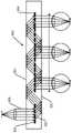
- Prior art date
- Legal status (The legal status is an assumption and is not a legal conclusion. Google has not performed a legal analysis and makes no representation as to the accuracy of the status listed.)
- Granted
Links
Images


Classifications
- G—PHYSICS
- G03—PHOTOGRAPHY; CINEMATOGRAPHY; ANALOGOUS TECHNIQUES USING WAVES OTHER THAN OPTICAL WAVES; ELECTROGRAPHY; HOLOGRAPHY
- G03H—HOLOGRAPHIC PROCESSES OR APPARATUS
- G03H1/00—Holographic processes or apparatus using light, infrared or ultraviolet waves for obtaining holograms or for obtaining an image from them; Details peculiar thereto
- G03H1/04—Processes or apparatus for producing holograms
- G03H1/20—Copying holograms by holographic, i.e. optical means
- G—PHYSICS
- G02—OPTICS
- G02B—OPTICAL ELEMENTS, SYSTEMS OR APPARATUS
- G02B27/00—Optical systems or apparatus not provided for by any of the groups G02B1/00 - G02B26/00, G02B30/00
- G02B27/0081—Optical systems or apparatus not provided for by any of the groups G02B1/00 - G02B26/00, G02B30/00 with means for altering, e.g. enlarging, the entrance or exit pupil
- G—PHYSICS
- G02—OPTICS
- G02B—OPTICAL ELEMENTS, SYSTEMS OR APPARATUS
- G02B27/00—Optical systems or apparatus not provided for by any of the groups G02B1/00 - G02B26/00, G02B30/00
- G02B27/01—Head-up displays
- G02B27/0101—Head-up displays characterised by optical features
- G02B27/0103—Head-up displays characterised by optical features comprising holographic elements
- G—PHYSICS
- G02—OPTICS
- G02B—OPTICAL ELEMENTS, SYSTEMS OR APPARATUS
- G02B27/00—Optical systems or apparatus not provided for by any of the groups G02B1/00 - G02B26/00, G02B30/00
- G02B27/01—Head-up displays
- G02B27/017—Head mounted
- G02B27/0172—Head mounted characterised by optical features
- G—PHYSICS
- G02—OPTICS
- G02B—OPTICAL ELEMENTS, SYSTEMS OR APPARATUS
- G02B6/00—Light guides; Structural details of arrangements comprising light guides and other optical elements, e.g. couplings
- G—PHYSICS
- G03—PHOTOGRAPHY; CINEMATOGRAPHY; ANALOGOUS TECHNIQUES USING WAVES OTHER THAN OPTICAL WAVES; ELECTROGRAPHY; HOLOGRAPHY
- G03H—HOLOGRAPHIC PROCESSES OR APPARATUS
- G03H1/00—Holographic processes or apparatus using light, infrared or ultraviolet waves for obtaining holograms or for obtaining an image from them; Details peculiar thereto
- G03H1/02—Details of features involved during the holographic process; Replication of holograms without interference recording
- G03H1/024—Hologram nature or properties
- G03H1/0248—Volume holograms
- G—PHYSICS
- G03—PHOTOGRAPHY; CINEMATOGRAPHY; ANALOGOUS TECHNIQUES USING WAVES OTHER THAN OPTICAL WAVES; ELECTROGRAPHY; HOLOGRAPHY
- G03H—HOLOGRAPHIC PROCESSES OR APPARATUS
- G03H1/00—Holographic processes or apparatus using light, infrared or ultraviolet waves for obtaining holograms or for obtaining an image from them; Details peculiar thereto
- G03H1/04—Processes or apparatus for producing holograms
- G03H1/0402—Recording geometries or arrangements
- G03H1/0408—Total internal reflection [TIR] holograms, e.g. edge lit or substrate mode holograms
- G—PHYSICS
- G03—PHOTOGRAPHY; CINEMATOGRAPHY; ANALOGOUS TECHNIQUES USING WAVES OTHER THAN OPTICAL WAVES; ELECTROGRAPHY; HOLOGRAPHY
- G03H—HOLOGRAPHIC PROCESSES OR APPARATUS
- G03H1/00—Holographic processes or apparatus using light, infrared or ultraviolet waves for obtaining holograms or for obtaining an image from them; Details peculiar thereto
- G03H1/04—Processes or apparatus for producing holograms
- G03H1/20—Copying holograms by holographic, i.e. optical means
- G03H1/202—Contact copy when the reconstruction beam for the master H1 also serves as reference beam for the copy H2
- G—PHYSICS
- G03—PHOTOGRAPHY; CINEMATOGRAPHY; ANALOGOUS TECHNIQUES USING WAVES OTHER THAN OPTICAL WAVES; ELECTROGRAPHY; HOLOGRAPHY
- G03H—HOLOGRAPHIC PROCESSES OR APPARATUS
- G03H1/00—Holographic processes or apparatus using light, infrared or ultraviolet waves for obtaining holograms or for obtaining an image from them; Details peculiar thereto
- G03H1/26—Processes or apparatus specially adapted to produce multiple sub- holograms or to obtain images from them, e.g. multicolour technique
- G—PHYSICS
- G02—OPTICS
- G02B—OPTICAL ELEMENTS, SYSTEMS OR APPARATUS
- G02B6/00—Light guides; Structural details of arrangements comprising light guides and other optical elements, e.g. couplings
- G02B6/10—Light guides; Structural details of arrangements comprising light guides and other optical elements, e.g. couplings of the optical waveguide type
- G02B6/12—Light guides; Structural details of arrangements comprising light guides and other optical elements, e.g. couplings of the optical waveguide type of the integrated circuit kind
- G02B2006/12083—Constructional arrangements
- G02B2006/12107—Grating
- G—PHYSICS
- G02—OPTICS
- G02B—OPTICAL ELEMENTS, SYSTEMS OR APPARATUS
- G02B6/00—Light guides; Structural details of arrangements comprising light guides and other optical elements, e.g. couplings
- G02B6/10—Light guides; Structural details of arrangements comprising light guides and other optical elements, e.g. couplings of the optical waveguide type
- G02B6/12—Light guides; Structural details of arrangements comprising light guides and other optical elements, e.g. couplings of the optical waveguide type of the integrated circuit kind
- G02B2006/12166—Manufacturing methods
- G02B2006/1219—Polymerisation
- G—PHYSICS
- G02—OPTICS
- G02B—OPTICAL ELEMENTS, SYSTEMS OR APPARATUS
- G02B27/00—Optical systems or apparatus not provided for by any of the groups G02B1/00 - G02B26/00, G02B30/00
- G02B27/01—Head-up displays
- G02B27/017—Head mounted
- G02B27/0172—Head mounted characterised by optical features
- G02B2027/0174—Head mounted characterised by optical features holographic
- G—PHYSICS
- G02—OPTICS
- G02B—OPTICAL ELEMENTS, SYSTEMS OR APPARATUS
- G02B27/00—Optical systems or apparatus not provided for by any of the groups G02B1/00 - G02B26/00, G02B30/00
- G02B27/0093—Optical systems or apparatus not provided for by any of the groups G02B1/00 - G02B26/00, G02B30/00 with means for monitoring data relating to the user, e.g. head-tracking, eye-tracking
- G—PHYSICS
- G03—PHOTOGRAPHY; CINEMATOGRAPHY; ANALOGOUS TECHNIQUES USING WAVES OTHER THAN OPTICAL WAVES; ELECTROGRAPHY; HOLOGRAPHY
- G03H—HOLOGRAPHIC PROCESSES OR APPARATUS
- G03H1/00—Holographic processes or apparatus using light, infrared or ultraviolet waves for obtaining holograms or for obtaining an image from them; Details peculiar thereto
- G03H1/04—Processes or apparatus for producing holograms
- G03H1/0402—Recording geometries or arrangements
- G03H2001/0439—Recording geometries or arrangements for recording Holographic Optical Element [HOE]
- G—PHYSICS
- G03—PHOTOGRAPHY; CINEMATOGRAPHY; ANALOGOUS TECHNIQUES USING WAVES OTHER THAN OPTICAL WAVES; ELECTROGRAPHY; HOLOGRAPHY
- G03H—HOLOGRAPHIC PROCESSES OR APPARATUS
- G03H1/00—Holographic processes or apparatus using light, infrared or ultraviolet waves for obtaining holograms or for obtaining an image from them; Details peculiar thereto
- G03H1/04—Processes or apparatus for producing holograms
- G03H1/20—Copying holograms by holographic, i.e. optical means
- G03H2001/205—Subdivided copy, e.g. scanning transfer
- G—PHYSICS
- G03—PHOTOGRAPHY; CINEMATOGRAPHY; ANALOGOUS TECHNIQUES USING WAVES OTHER THAN OPTICAL WAVES; ELECTROGRAPHY; HOLOGRAPHY
- G03H—HOLOGRAPHIC PROCESSES OR APPARATUS
- G03H1/00—Holographic processes or apparatus using light, infrared or ultraviolet waves for obtaining holograms or for obtaining an image from them; Details peculiar thereto
- G03H1/22—Processes or apparatus for obtaining an optical image from holograms
- G03H1/2202—Reconstruction geometries or arrangements
- G03H2001/2223—Particular relationship between light source, hologram and observer
- G03H2001/2226—Edge lit holograms
- G—PHYSICS
- G03—PHOTOGRAPHY; CINEMATOGRAPHY; ANALOGOUS TECHNIQUES USING WAVES OTHER THAN OPTICAL WAVES; ELECTROGRAPHY; HOLOGRAPHY
- G03H—HOLOGRAPHIC PROCESSES OR APPARATUS
- G03H2223/00—Optical components
- G03H2223/16—Optical waveguide, e.g. optical fibre, rod
- G—PHYSICS
- G03—PHOTOGRAPHY; CINEMATOGRAPHY; ANALOGOUS TECHNIQUES USING WAVES OTHER THAN OPTICAL WAVES; ELECTROGRAPHY; HOLOGRAPHY
- G03H—HOLOGRAPHIC PROCESSES OR APPARATUS
- G03H2260/00—Recording materials or recording processes
Landscapes
- Physics & Mathematics (AREA)
- General Physics & Mathematics (AREA)
- Optics & Photonics (AREA)
- Diffracting Gratings Or Hologram Optical Elements (AREA)
- Holo Graphy (AREA)
- Optical Integrated Circuits (AREA)
Abstract
Translated fromChinese
Description
Translated fromChinese本申请是国际申请日为2019年1月8日、国家申请号为201980007747.0、发明名称为“用于制造光学波导的方法”的发明专利申请的分案申请。This application is a divisional application of an invention patent application with an international filing date of January 8, 2019, a national application number of 201980007747.0, and an invention title of "Method for Manufacturing Optical Waveguides".
技术领域technical field
本发明一般地涉及用于波导的制造的方法,并且更具体地用于波导显示器。The present invention relates generally to methods for the manufacture of waveguides, and more particularly to waveguide displays.
背景技术Background technique
波导可以被称为具有限制和引导波的能力的结构(即,限制波可以在其中传播的空间区域)。一个子类包括光学波导,光学波导是可以引导典型地在可见光谱中的电磁波的结构。波导结构可以被设计为使用许多不同的机构来控制波的传播路径。例如,平面波导可以被设计为利用衍射光栅来衍射和耦合入射光到波导结构内,使得入耦合光(in-coupledlight)可以经由全内反射(“TIR”)在平面结构内继续行进。A waveguide can be referred to as a structure that has the ability to confine and guide waves (ie, confine the region of space in which waves can propagate). A subclass includes optical waveguides, which are structures that can guide electromagnetic waves, typically in the visible spectrum. Waveguide structures can be designed to use many different mechanisms to control the propagation paths of waves. For example, planar waveguides can be designed to utilize diffraction gratings to diffract and couple incident light into the waveguide structure so that in-coupled light can continue to travel within the planar structure via total internal reflection ("TIR").
波导的制造可以包括允许在波导内记录全息光学元件的材料系统的使用。一类这样的材料包括聚合物分散的液晶(“PDLC”)混合物,该PDLC混合物是包含光聚合单体和液晶的混合物。这样的混合物的另一子类包括全息聚合物分散的液晶(“HPDLC”)混合物。可以通过用两个相互相干的激光波束对材料照明来将诸如体相位光栅之类的全息光学元件记录在这样的液体混合物中。在记录过程期间,单体聚合并且混合物经历光聚合引发的相分离,从而产生被液晶微滴密集填充的区域,其间散布着清聚合物(clear polymer)区域。交替的富液晶区域和贫液晶区域形成光栅的条纹平面。Fabrication of the waveguides may include the use of material systems that allow the recording of holographic optical elements within the waveguides. One class of such materials includes polymer dispersed liquid crystal ("PDLC") mixtures, which are mixtures comprising photopolymerizable monomers and liquid crystals. Another subclass of such mixtures includes holographic polymer dispersed liquid crystal ("HPDLC") mixtures. Holographic optical elements such as volume phase gratings can be recorded in such liquid mixtures by illuminating the material with two mutually coherent laser beams. During the recording process, the monomers polymerize and the mixture undergoes photopolymerization-induced phase separation, resulting in regions densely packed with liquid crystal droplets interspersed with clear polymer regions. The alternating LC-rich and LC-poor regions form the fringe planes of the grating.
诸如上面所描述的波导光学器件可以被考虑用于一系列显示器和传感器应用。在许多应用中,可以使用各种波导体系和材料系统来实现包含编码多种光学功能的一个或多个光栅层的波导,从而使得在用于增强现实(“AR”)和虚拟现实(“VR”)的近眼显示器、用于航空和陆路运输的紧凑型抬头显示器(“HUD”)以及用于生物识别(biometric)和激光雷达(“LIDAR”)应用的传感器中能够有新的创新。Waveguide optics such as those described above can be considered for a range of display and sensor applications. In many applications, a variety of waveguide systems and material systems can be used to implement waveguides containing one or more grating layers encoding a variety of optical functions, enabling applications in augmented reality ("AR") and virtual reality ("VR") ”), compact head-up displays (“HUDs”) for air and land transportation, and sensors for biometric and lidar (“LIDAR”) applications.
发明内容SUMMARY OF THE INVENTION
一个实施例包括一种用于记录全息图的方法,所述方法包括:提供波导单元(cell),所述波导单元包括夹在两个基板之间的聚合物分散的液晶混合物层,提供母版光栅,朝向所述母版光栅发射至少一个记录波束,其中在与所述母版光栅相互作用后,所述至少一个记录波束的一部分朝向所述波导单元衍射,以及使用至少由所述至少一个记录波束的衍射部分形成的干涉曝光在所述波导单元内记录至少一个体光栅。One embodiment includes a method for recording a hologram, the method comprising: providing a waveguide cell comprising a layer of polymer dispersed liquid crystal mixture sandwiched between two substrates, providing a master a grating that emits at least one recording beam towards the master grating, wherein after interacting with the master grating a portion of the at least one recording beam is diffracted towards the waveguide unit, and using at least one recording beam generated by the at least one recording The interferometric exposure formed by the diffracted portion of the beam records at least one volume grating within the waveguide unit.
进一步的实施例还包括一种用于记录全息光栅的系统,所述系统包括波导单元,所述波导单元包括夹在两个基板之间的聚合物分散的液晶混合物层,母版光栅,被配置为朝向所述母版光栅发射至少一个记录波束的光源,其中在与所述母版光栅相互作用后,所述至少一个记录波束的一部分朝向所述波导单元衍射并且通过至少由所述至少一个记录波束的衍射部分形成的干涉曝光在所述波导单元内记录至少一个体光栅。Further embodiments also include a system for recording a holographic grating, the system comprising a waveguide unit comprising a layer of polymer dispersed liquid crystal mixture sandwiched between two substrates, a master grating, configured is a light source that emits at least one recording beam towards the master grating, wherein after interacting with the master grating a portion of the at least one recording beam is diffracted towards the waveguide unit and passed through at least one recording beam by the at least one recording beam The interferometric exposure formed by the diffracted portion of the beam records at least one volume grating within the waveguide unit.
在另一个实施例中,所述母版光栅包括振幅光栅。In another embodiment, the master grating comprises an amplitude grating.
在进一步的实施例中,所述母版光栅包括啁啾光栅。In further embodiments, the master grating comprises a chirped grating.
在又一个实施例中,记录的所述体光栅包含滚动的K向量。In yet another embodiment, the recorded volume raster contains rolled K-vectors.
在又进一步的实施例中,记录的所述体光栅包含复用光栅。In yet further embodiments, the recorded volume gratings comprise multiplexed gratings.
在再一个实施例中,所述母版光栅包括三个单独的光栅。In yet another embodiment, the master grating includes three separate gratings.
在再进一步的实施例中,三个单独的光栅被设计为记录输入光栅、折叠光栅以及输出光栅。In still further embodiments, three separate gratings are designed to record the input grating, the folded grating and the output grating.
在另一个附加的实施例中,所述至少一个体光栅包括三个体光栅。In another additional embodiment, the at least one volume grating includes three volume gratings.
在进一步附加的实施例中,所述至少一个记录波束包括三个记录波束。In further additional embodiments, the at least one recording beam includes three recording beams.
在还有一个实施例中,所述干涉曝光由仅一个记录波束的零级波束和衍射部分形成。In yet another embodiment, the interferometric exposure is formed by the zero-order beam and diffractive portion of only one recording beam.
附加的实施例和特征在下面的描述中被某种程度上阐述,并且在审阅说明书后对于本领域技术人员将在某种程度上变得清楚,或者可以通过实践本发明而被认识到。通过参考形成本公开的一部分的附图和说明书的剩余部分,可以实现对本发明的性质和优点的进一步理解。Additional embodiments and features are set forth in the following description to the extent that they will become apparent to those skilled in the art upon review of the specification, or may be recognized by practice of the invention. A further understanding of the nature and advantages of the present invention may be realized by reference to the accompanying drawings and the remainder of the specification which form a part of this disclosure.
附图说明Description of drawings
参考下面的附图和数据图将更充分地理解本描述,这些附图和数据图被呈现为本发明的示例性实施例,并且不应被解释为对本发明范围的完全阐述。对于本领域技术人员将清楚的是,可以用下面描述中所公开的本发明的一些或全部来实践本发明。The present description will be more fully understood by reference to the following drawings and data diagrams, which are presented as exemplary embodiments of the invention and should not be construed as exhaustive of the scope of the invention. It will be apparent to those skilled in the art that the present invention may be practiced with some or all of the invention disclosed in the following description.
图1A和图1B概念性地图示了根据本发明的各种实施例的两种体布拉格光栅配置。1A and 1B conceptually illustrate two volume Bragg grating configurations in accordance with various embodiments of the present invention.
图2概念性地图示了根据本发明的实施例的表面形貌光栅(surface reliefgrating)。Figure 2 conceptually illustrates a surface relief grating according to an embodiment of the invention.
图3A和图3B概念性地图示了根据本发明的各种实施例的HPDLC SBG设备和SBG的开关特性。3A and 3B conceptually illustrate switching characteristics of HPDLC SBG devices and SBGs in accordance with various embodiments of the present invention.
图4A-图4D概念性地图示了根据本发明的各种实施例的两波束记录过程。4A-4D conceptually illustrate a two-beam recording process according to various embodiments of the present invention.
图5概念性地图示了根据本发明的实施例的利用振幅光栅的单波束记录过程。Figure 5 conceptually illustrates a single beam recording process utilizing an amplitude grating according to an embodiment of the present invention.
图6A和图6B概念性地图示了根据本发明的各种实施例的滚动的K向量光栅的两种实施方式。6A and 6B conceptually illustrate two implementations of a rolling K-vector grating in accordance with various embodiments of the present invention.
图7概念性地图示了根据本发明的实施例的复用K向量光栅。Figure 7 conceptually illustrates a multiplexed K-vector grating in accordance with an embodiment of the present invention.
图8概念性地图示了根据本发明的实施例的利用耦合光栅将光衍射进和出波导的波导。8 conceptually illustrates a waveguide utilizing a coupling grating to diffract light into and out of the waveguide in accordance with an embodiment of the present invention.
图9和图10概念性地图示了根据本发明的实施例的将输出光栅用于在一个维度上的出射光瞳扩展的波导。9 and 10 conceptually illustrate waveguides using an output grating for exit pupil expansion in one dimension, according to embodiments of the present invention.
图11概念性地图示了根据本发明的实施例的利用两个平面波导来提供在两个维度上的出射光瞳扩展的波导系统。Figure 11 conceptually illustrates a waveguide system utilizing two planar waveguides to provide exit pupil expansion in two dimensions in accordance with an embodiment of the present invention.
图12概念性地图示了根据本发明的实施例的利用三光栅结构来提供二维出射光瞳扩展的波导。12 conceptually illustrates a waveguide utilizing a triple grating structure to provide a two-dimensional exit pupil expansion according to an embodiment of the present invention.
图13概念性地图示了根据本发明的实施例的波导的RGB堆叠的剖面视图。13 conceptually illustrates a cross-sectional view of an RGB stack of waveguides in accordance with an embodiment of the present invention.
图14概念性地图示了根据本发明的实施例的具有两个光栅层的双轴扩展波导显示器。Figure 14 conceptually illustrates a biaxial extended waveguide display with two grating layers in accordance with an embodiment of the present invention.
图15概念性地图示了根据本发明的实施例的单个光栅层的平面视图。Figure 15 conceptually illustrates a plan view of a single grating layer in accordance with an embodiment of the present invention.
图16概念性地图示了根据本发明的实施例的两个光栅层配置的平面视图。Figure 16 conceptually illustrates a plan view of a two grating layer configuration in accordance with an embodiment of the present invention.
图17概念性地图示了根据本发明的实施例的双轴扩展波导显示器。17 conceptually illustrates a dual-axis extended waveguide display according to an embodiment of the present invention.
图18概念性地图示了根据本发明的实施例的眼动跟踪显示器。18 conceptually illustrates an eye-tracking display according to an embodiment of the present invention.
图19概念性地图示了根据本发明的实施例的具有动态聚焦元件和眼动跟踪器的双扩展波导显示器。19 conceptually illustrates a dual extended waveguide display with dynamic focusing elements and eye trackers in accordance with an embodiment of the present invention.
图20A和图20B概念性地图示了根据本发明的实施例的通过光-机械接口耦合到输入图像节点的波导显示器。20A and 20B conceptually illustrate a waveguide display coupled to an input image node through an opto-mechanical interface in accordance with an embodiment of the present invention.
图21-图24概念性地图示了根据本发明的各种实施例的各种输入图像节点配置。21-24 conceptually illustrate various input image node configurations in accordance with various embodiments of the present invention.
图25概念性地图示了根据本发明的实施例的示出了用于波导显示器的部件的系统图。25 conceptually illustrates a system diagram showing components for a waveguide display in accordance with an embodiment of the present invention.
图26概念性地图示了根据本发明的实施例的利用啁啾振幅光栅的曝光过程。26 conceptually illustrates an exposure process utilizing a chirped amplitude grating according to an embodiment of the present invention.
图27A和图27B概念性地图示了根据本发明的实施例的用于同时形成三个光栅的曝光过程。27A and 27B conceptually illustrate an exposure process for simultaneously forming three gratings according to an embodiment of the present invention.
图28概念性地图示了根据本发明的实施例的用于同时曝光红光栅、蓝光栅和绿光栅的制造设置。28 conceptually illustrates a fabrication setup for simultaneously exposing red, blue, and green gratings in accordance with an embodiment of the present invention.
图29A-图29C概念性地图示了根据本发明的各种实施例的用于生成RKV光栅的各种方法。29A-29C conceptually illustrate various methods for generating RKV gratings in accordance with various embodiments of the present invention.
图30A和图30B概念性地图示了根据本发明的各种实施例的啁啾光栅的各种应用。30A and 30B conceptually illustrate various applications of chirped gratings in accordance with various embodiments of the present invention.
图31概念性地图示了根据本发明的实施例的利用零级光栅连同啁啾光栅的母版系统(mastering system)。31 conceptually illustrates a mastering system utilizing a zero-order grating in conjunction with a chirped grating, according to an embodiment of the present invention.
图32概念性地图示了根据本发明的实施例的利用参考光栅的母版系统。Figure 32 conceptually illustrates a mastering system utilizing a reference raster according to an embodiment of the present invention.
图33概念性地图示了根据本发明的实施例的母版系统,该母版系统被配置为避免产生其它级次波束和/或避免干扰聚焦在液晶基板上的能量波束。33 conceptually illustrates a mastering system configured to avoid generating additional sub-beams and/or to avoid interfering with energy beams focused on a liquid crystal substrate, according to an embodiment of the present invention.
图34概念性地图示了母版光栅的位置对结果所得的衍射的影响。Figure 34 conceptually illustrates the effect of the position of the master grating on the resulting diffraction.
具体实施方式Detailed ways
为了描述实施例的目的,已省略或简化了光学设计和视觉显示器领域中的技术人员已知的光学技术的一些众所周知的特征,以免模糊本发明的基本原理。除非另有陈述,否则关于光线或波束方向的术语“同轴(on-axis)”是指与垂直于关于本发明所描述的光学部件的表面的轴平行的传播。在下面的描述中,术语光、光线、波束和方向可以被互换使用并且彼此相关联,以指示电磁辐射的沿着直线轨迹的传播的方向。关于电磁光谱的可见波段和红外波段,可以使用术语光和照明。下面描述的部分将使用光学设计领域中的技术人员通常所采用的术语来陈述。如本文所使用的,在一些实施例中,术语光栅可以涵盖包括光栅集合的光栅。为了说明的目的,要理解的是,除非另有陈述,否则附图未按比例绘制。For the purpose of describing the embodiments, some well-known features of optical technology known to those skilled in the art of optical design and visual displays have been omitted or simplified in order not to obscure the underlying principles of the invention. Unless otherwise stated, the term "on-axis" with respect to a ray or beam direction refers to propagation parallel to an axis perpendicular to the surfaces of the optical components described with respect to this invention. In the following description, the terms light, ray, beam and direction may be used interchangeably and in relation to each other to indicate the direction of propagation of electromagnetic radiation along a linear trajectory. With regard to the visible and infrared bands of the electromagnetic spectrum, the terms light and illumination can be used. Portions of the following description will be presented using terminology commonly employed by those skilled in the art of optical design. As used herein, in some embodiments, the term raster may encompass a raster comprising a collection of rasters. For illustrative purposes, it is to be understood that the drawings are not drawn to scale unless otherwise stated.
现在转到附图,描述了母版系统以及使用这样的母版系统来制造波导和波导设备的方法。用于制造全息波导的母版系统可以包括使用母版来控制能量(例如,激光、光或磁波束)在液晶基板上的施加,以在液晶基板内制造全息波导。在制造之后,可以将完成的全息波导结合到各种显示系统内。这些母版系统可以采用一个或多个能量波束。在许多实施例中,母版系统使用单个能量波束,其可以简化母版系统内各种部件的对准,并且可以减少在两波束系统中发现的由两个波束的不同路径引起的波前误差。照此,单能量波束过程可以与其中热和振动考虑可能在对准多个能量波束中引入各种复杂性的大体量制造过程兼容。根据本发明的实施例的用于制造全息波导的母版系统可以包括各种特征。这些特征包括但不限于:用于单个输入波束复本的啁啾(即,接近混合接触复本)、双啁啾光栅(用于输入和输出)、用于透射控制的零级光栅、对准参考光栅、3:1构造、位置调整工具以使得能够快速对准、同时优化多个滚动的K向量光栅的透镜和窗口厚度,以及衍射波束的交叉和其它级次的避免。在以下部分中进一步详细地描述波导结构、母版系统和曝光过程。Turning now to the drawings, a mastering system and methods of fabricating waveguides and waveguide devices using such mastering systems are described. A mastering system for fabricating holographic waveguides may include using a mastering master to control the application of energy (eg, laser, optical, or magnetic beams) on a liquid crystal substrate to fabricate holographic waveguides within the liquid crystal substrate. After fabrication, the completed holographic waveguide can be incorporated into various display systems. These master systems can employ one or more energy beams. In many embodiments, the mastering system uses a single beam of energy, which can simplify the alignment of various components within the mastering system and can reduce wavefront errors found in two-beam systems caused by the different paths of the two beams . As such, a single energy beam process may be compatible with high volume manufacturing processes where thermal and vibrational considerations may introduce various complexities in aligning multiple energy beams. A master system for fabricating holographic waveguides according to embodiments of the present invention may include various features. These features include, but are not limited to: chirp for single input beam replica (ie, near hybrid contact replica), double chirped grating (for input and output), zero-order grating for transmission control, alignment Reference gratings, 3:1 configuration, position adjustment tools to enable rapid alignment, simultaneous optimization of lens and window thicknesses for multiple rolling K-vector gratings, and avoidance of diffraction beam crossings and other orders. The waveguide structure, master system and exposure process are described in further detail in the following sections.
波导结构waveguide structure
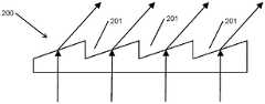
根据各种实施例的波导结构可以以许多不同的方式实现。在许多实施例中,波导结构被设计为光学波导,其为可以限制和引导在可见光谱中的电磁波或光的结构。这些光学波导可以被实现用在许多不同的应用中,诸如但不限于头盔安装的显示器、头戴式显示器(“HMD”)和HUD。术语HUD通常用于描述结合了透明显示器的一类设备,该透明显示器呈现数据而无需用户改变其通常的视场。光学波导可以取决于给定的应用将各种光学功能集成到期望的形状因子(form factor)内。Waveguide structures according to various embodiments can be implemented in many different ways. In many embodiments, the waveguide structures are designed as optical waveguides, which are structures that can confine and guide electromagnetic waves or light in the visible spectrum. These optical waveguides can be implemented for use in many different applications, such as, but not limited to, helmet mounted displays, head mounted displays ("HMD"), and HUDs. The term HUD is often used to describe a class of devices that incorporate a transparent display that presents data without requiring the user to change their usual field of view. Optical waveguides can integrate various optical functions into a desired form factor depending on the given application.
根据各种实施例的光学波导可以被设计为使用各种方法和波导光学器件以受控的方式来操纵光波。例如,可以使用具有比周围环境更高的折射率的材料来实现光学波导,以限制光可以在其中传播的区域。可以经由全内反射将以特定角度耦合到由这样的材料制成的光学波导内的光限制在波导内。在平面波导中,发生全内反射的角度可以由斯涅尔定律给出,该斯涅尔定律可以确定光在表面边界处是折射还是全反射。Optical waveguides according to various embodiments can be designed to manipulate light waves in a controlled manner using various methods and waveguide optics. For example, optical waveguides can be implemented using materials that have a higher index of refraction than the surrounding environment to limit the area in which light can propagate. Light coupled at a specific angle into an optical waveguide made of such materials can be confined within the waveguide via total internal reflection. In planar waveguides, the angle at which total internal reflection occurs can be given by Snell's law, which determines whether light is refracted or totally reflected at surface boundaries.
在许多实施例中,结合布拉格光栅的波导被实现用于HUD应用。HUD可以被结合在各种应用的任何应用中,包括(但不限于)近眼应用。与使用常规光学部件实现的HUD相比,根据本发明的各种实施例的利用结合了布拉格光栅的平面波导的HUD可以实现显著更大的视场并具有更低的体积要求。在一些实施例中,HUD包括结合许多光栅的至少一个波导。在进一步的实施例中,波导结合可以被实现为提供各种光学功能(诸如但不限于双轴波束扩展)的至少三个布拉格光栅。例如,在许多实施例中,波导结合输入光栅、折叠光栅以及输出光栅。可以使用变化数量的波导来实现利用波导的HUD。在许多实施例中,使用单个波导来实现HUD。在其它实施例中,使用波导的堆叠来实现HUD。多个波导可以被堆叠并被实现为提供不同的光学功能,诸如但不限于实现彩色显示器。在若干实施例中,HUD结合三个单独的波导,针对红、绿和蓝色彩通道中的每个有一个波导。In many embodiments, waveguides incorporating Bragg gratings are implemented for HUD applications. A HUD can be incorporated in any of a variety of applications, including but not limited to near-eye applications. HUDs utilizing planar waveguides incorporating Bragg gratings according to various embodiments of the present invention can achieve significantly larger fields of view and have lower volume requirements than HUDs implemented using conventional optics. In some embodiments, the HUD includes at least one waveguide incorporating a number of gratings. In further embodiments, the waveguide combination may be implemented as at least three Bragg gratings that provide various optical functions such as, but not limited to, biaxial beam spreading. For example, in many embodiments, the waveguide incorporates an input grating, a folded grating, and an output grating. HUDs utilizing waveguides can be implemented using varying numbers of waveguides. In many embodiments, the HUD is implemented using a single waveguide. In other embodiments, the HUD is implemented using a stack of waveguides. Multiple waveguides can be stacked and implemented to provide different optical functions, such as but not limited to implementing a color display. In several embodiments, the HUD incorporates three separate waveguides, one for each of the red, green, and blue color channels.
根据本发明的各种实施例的利用布拉格光栅的波导可以被设计为具有不同类型的条纹。具有相同的表面节距尺寸但不同的光栅倾斜角的多个波导的使用可以增大波导的整体耦合入角带宽(couple-in angular bandwidth)。在许多实施例中,波导内的光栅中的一个或多个光栅结合跨光栅变化的倾斜角和/或滚动K向量,以修改光栅的衍射效率。K向量可以被定义为与相关联的光栅条纹的平面正交的向量,其可以确定给定范围的输入和衍射角的光学效率。通过结合具有滚动的K向量(“RKV”)的光栅,光栅可以被设计为以实现在HUD显示器的眼动范围(eyebox)上的期望特点的方式来改变衍射效率。以下进一步详细讨论光栅条纹的配置(诸如RKV)以及与用在HUD中的波导的结构和实施方式相关的其它方面。Waveguides utilizing Bragg gratings according to various embodiments of the present invention may be designed to have different types of fringes. The use of multiple waveguides with the same surface pitch size but different grating tilt angles can increase the overall couple-in angular bandwidth of the waveguides. In many embodiments, one or more of the gratings within the waveguide incorporates varying tilt angles and/or rolling K-vectors across the gratings to modify the diffraction efficiency of the gratings. The K vector can be defined as the vector normal to the plane of the associated grating fringes that can determine the optical efficiency for a given range of input and diffraction angles. By incorporating gratings with rolling K-vectors ("RKV"), the gratings can be designed to vary diffraction efficiency in a manner that achieves desired characteristics over the eyebox of the HUD display. The configuration of grating fringes, such as RKVs, and other aspects related to the structure and implementation of waveguides used in HUDs are discussed in further detail below.
衍射光栅Diffraction grating
光学波导可以结合不同的光学元件以操纵光波的传播。如可以容易地认识到的,所选择的光栅的类型可以取决于给定应用的具体要求。被记录在波导中的光学结构可以包括许多不同类型的光学元件,诸如但不限于衍射光栅。在许多实施例中,实现的光栅是布拉格光栅(也被称为体光栅)。布拉格光栅可以具有高的效率,其中几乎没有光被衍射到更高级次内。可以通过控制光栅的折射率调制来改变光在衍射和零级中的相对量,该特性可以用于制作有损的波导光栅,用于提取大光瞳上的光。通过策略性地将体布拉格光栅放置在波导内,可以以受控的方式来影响波导内的光的传播,以实现各种效果。入射在光栅上的光的衍射可以由光栅和光的特点确定。如可以容易地认识到的,取决于给定应用的具体要求,体布拉格光栅可以被构造为具有不同的特点。在许多实施例中,体布拉格光栅被设计为透射光栅。在其它实施例中,体布拉格光栅被设计为反射光栅。在透射光栅中,满足布拉格条件的入射光被衍射,使得衍射光在入射光的未进入侧离开光栅。对于反射光栅,衍射光在光栅的入射光进入的同一侧出射。Optical waveguides can incorporate different optical elements to manipulate the propagation of light waves. As can be readily appreciated, the type of grating selected may depend on the specific requirements of a given application. The optical structures recorded in the waveguide may include many different types of optical elements, such as, but not limited to, diffraction gratings. In many embodiments, the gratings implemented are Bragg gratings (also known as volume gratings). Bragg gratings can have high efficiencies where little light is diffracted into higher orders. The relative amount of light in diffraction and the zeroth order can be changed by controlling the refractive index modulation of the grating, a property that can be used to make lossy waveguide gratings for light extraction over large pupils. By strategically placing volume Bragg gratings within the waveguide, the propagation of light within the waveguide can be influenced in a controlled manner to achieve various effects. The diffraction of light incident on the grating can be determined by the characteristics of the grating and the light. As can be readily appreciated, volume Bragg gratings can be constructed with different characteristics depending on the specific requirements of a given application. In many embodiments, the volume Bragg grating is designed as a transmission grating. In other embodiments, the volume Bragg grating is designed as a reflection grating. In a transmission grating, incident light satisfying the Bragg condition is diffracted so that the diffracted light leaves the grating on the non-entering side of the incident light. For reflective gratings, the diffracted light exits on the same side of the grating that the incident light entered.
图1A和图1B概念性地图示了根据本发明的各种实施例的两种体布拉格光栅配置。取决于在衍射之后光线自其出射的侧,可以将光栅分类为反射光栅100或是透射光栅150。折射/反射的条件或布拉格条件可以取决于若干因子,诸如但不限于介质的折射率、光栅周期、入射光的波长以及入射角。图1A示出了被记录在透明材料中的反射光栅100。如所示,光线101、102具有不同的波长并且以相同的角度入射在反射光栅100上,该反射光栅100具有与光栅表面平行的条纹103。光线101不满足布拉格条件,并被透射通过光栅。另一方面,光线102确实满足布拉格条件并被反射回通过其进入的同一表面。另一种类型的光栅是透射光栅,该透射光栅在图1B中被概念性地图示。在说明性实施例中,透射光栅150具有垂直于光栅表面的条纹151。如所示,具有不同波长的光线152、153以相同的角度入射在透射光栅150上。光线152满足布拉格条件并被折射,在光栅的光线152进入的相对侧上出射。光线153不满足布拉格条件,并按它原始的传播路径被透射通过。取决于光栅的效率,光可以被部分地反射或折射。虽然图1A和图1B图示了具体的体光栅结构,但是根据本发明的各种实施例,可以在波导单元(waveguide cell)中记录任何类型的光栅结构。例如,体光栅可以用相对于光栅表面偏斜和/或倾斜的条纹来实现,这些条纹可以影响衍射/反射的角度。虽然以上的讨论将光栅结构表示为透射或是反射,但是根据标准光栅方程,两种类型的光栅均可以以相同的方式表现。1A and 1B conceptually illustrate two volume Bragg grating configurations in accordance with various embodiments of the present invention. Depending on the side from which the light exits after diffraction, the grating can be classified as either a
根据本发明的各种实施例的波导结构可以以许多不同的方式来实现光栅。除了体光栅之外,光栅还可以被实现为表面形貌光栅。顾名思义,可以通过在基板的表面上物理地形成凹槽或周期性图案来实现表面形貌光栅。由凹槽形成的周期性和角度可以确定光栅的效率和其它特点。许多方法中的任何方法都可以被用于形成这些凹槽,诸如但不限于蚀刻和光刻。Waveguide structures according to various embodiments of the present invention can implement gratings in many different ways. In addition to volume gratings, gratings can also be implemented as surface topography gratings. As the name suggests, surface topography gratings can be achieved by physically forming grooves or periodic patterns on the surface of the substrate. The periodicity and angle formed by the grooves can determine the efficiency and other characteristics of the grating. Any of a number of methods can be used to form these grooves, such as, but not limited to, etching and photolithography.
图2概念性地图示了根据本发明的实施例的表面形貌光栅。如所示,表面形貌光栅200包含周期性倾斜的凹槽201。当光入射在凹槽201上时,在某些条件下可以发生衍射。凹槽201的倾斜和周期性可以被设计为实现入射光的目标衍射行为。Figure 2 conceptually illustrates a surface topography grating according to an embodiment of the invention. As shown, the surface topography grating 200 includes periodically sloped
虽然图1A-图1B和图2示出了具体的光栅结构,但容易认识到的是,可以取决于给定应用的具体要求以许多不同的方式来配置光栅结构。在以下部分中进一步详细讨论这样的配置的示例。Although FIGS. 1A-1B and FIG. 2 illustrate specific grating structures, it is readily recognized that grating structures may be configured in many different ways depending on the specific requirements of a given application. Examples of such configurations are discussed in further detail in the following sections.
可开关布拉格光栅Switchable Bragg Gratings
全息波导设备中使用的一类光栅是可开关布拉格光栅(“SBG”)。可以通过首先在玻璃板或基板之间放置光聚合单体和液晶材料的混合物的薄膜来制造SBG。在许多情况下,玻璃板处于平行配置。一个或两个玻璃板可以支持电极,通常为透明的氧化锡膜,用于在膜上施加电场。可以通过使用具有空间周期性强度调制的干涉曝光来进行的光聚合引发的相分离,将SBG中的光栅结构记录在液体材料(通常被称为浆)中。诸如但不限于辐射强度的控制、混合物中材料的组分体积分数以及曝光温度之类的因子可以确定结果所得的光栅形态和性能。如可以容易地理解的,取决于给定应用的具体要求,可以使用多种材料和混合物。在许多实施例中,使用了HPDLC材料。在记录过程期间,单体聚合并且混合物经历相分离。LC分子聚集以形成离散的或聚结的微滴,这些微滴周期性地分布在光学波长尺度上的聚合物网络中。交替的富液晶区域和贫液晶区域形成光栅的条纹平面,其可以产生具有强光学偏振的布拉格衍射,该强光学偏振由微滴中LC分子的朝向排列产生。One type of grating used in holographic waveguide devices is the switchable Bragg grating ("SBG"). SBGs can be fabricated by first placing a thin film of a mixture of photopolymerizable monomers and liquid crystal material between glass plates or substrates. In many cases, the glass sheets are in a parallel configuration. One or two glass plates can support the electrodes, usually a transparent tin oxide film, which is used to apply an electric field across the film. Grating structures in SBGs can be recorded in liquid materials (often referred to as slurries) by photopolymerization-induced phase separation using interferometric exposure with spatially periodic intensity modulation. Factors such as, but not limited to, control of radiation intensity, component volume fractions of materials in the mixture, and exposure temperature can determine the resulting grating morphology and performance. As can be readily appreciated, a variety of materials and mixtures may be used depending on the specific requirements of a given application. In many embodiments, HPDLC material is used. During the recording process, the monomers polymerized and the mixture underwent phase separation. LC molecules aggregate to form discrete or coalesced droplets that are periodically distributed in a polymer network on the optical wavelength scale. The alternating LC-rich and LC-poor regions form the fringe planes of the grating, which can produce Bragg diffraction with strong optical polarization resulting from the orientation alignment of the LC molecules in the droplet.
结果所得的体相位光栅可以表现出非常高的衍射效率,该衍射效率可以通过施加在膜上的电场的大小来控制。当经由透明电极将电场施加到光栅时,LC液滴的自然朝向可以改变,从而引起条纹的折射率调制降低,并且全息衍射效率降低到非常低的水平。通常,电极被配置为使得所施加的电场将垂直于基板。在许多实施例中,电极由铟锡氧化物(“ITO”)制成。在没有施加电场的关断(OFF)状态下,液晶的非常轴通常垂直于条纹对准。因而,光栅对P-偏振光表现出高折射率调制和高衍射效率。当对HPDLC施加电场时,光栅切换到打开(ON)状态,其中液晶分子的非常轴平行于所施加的电场并因此垂直于基板对准。在ON状态下,光栅对S-偏振光和P-偏振光两者均表现出较低的折射率调制和较低的衍射效率。因而,光栅区域不再衍射光。根据HPDLC设备的功能,每个光栅区域可以被分成诸如例如像素基体之类的多重光栅元件。通常,在一个基板表面上的电极是均匀且连续的,而在相对的基板表面上的电极是根据多重可选择性开关光栅元件被图案化的。The resulting volume phase grating can exhibit very high diffraction efficiency, which can be controlled by the magnitude of the electric field applied to the film. When an electric field is applied to the grating via the transparent electrode, the natural orientation of the LC droplets can be changed, causing the refractive index modulation of the fringes to decrease and the holographic diffraction efficiency to drop to very low levels. Typically, the electrodes are configured such that the applied electric field will be perpendicular to the substrate. In many embodiments, the electrodes are made of indium tin oxide ("ITO"). In the off (OFF) state with no applied electric field, the extraordinary axis of the liquid crystal is generally aligned perpendicular to the stripes. Thus, the grating exhibits high refractive index modulation and high diffraction efficiency for P-polarized light. When an electric field is applied to the HPDLC, the grating switches to an open (ON) state in which the extraordinary axes of the liquid crystal molecules are aligned parallel to the applied electric field and thus perpendicular to the substrate. In the ON state, the grating exhibits lower refractive index modulation and lower diffraction efficiency for both S-polarized and P-polarized light. Thus, the grating regions no longer diffract light. Depending on the functionality of the HPDLC device, each grating region can be divided into multiple grating elements such as eg pixel substrates. Typically, the electrodes on one substrate surface are uniform and continuous, while the electrodes on the opposite substrate surface are patterned according to multiple selectively switchable grating elements.
通常,SBG元件在30μs内被开关清除,并用更长的驰豫时间被接通。注意到可以借助于所施加的电压在连续范围上调整设备的衍射效率。在许多情况下,设备在不施加电压的情况下表现出接近100%的效率,并在施加足够高的电压的情况下表现出基本上零效率。在某些类型的HPDLC设备中,磁场可以用于控制LC朝向。在一些HPDLC应用中,LC材料与聚合物的相分离可以达到不产生可辨别的微滴结构这样的程度。SBG也可以被用作无源光栅。在这个模式下,其主要优点是独特的高折射率调制。SBG可以用于为自由空间应用提供透射光栅或反射光栅。SBG可以被实现为波导设备,其中HPDLC形成波导附近的倏逝耦合层或是波导芯。用于形成HPDLC单元的玻璃板提供全内反射(“TIR”)光引导结构。当可开关光栅以超过TIR条件的角度衍射光时,可以将光耦合出SBG。Typically, the SBG element is cleared by the switch within 30 μs and turned on with a longer relaxation time. Note that the diffraction efficiency of the device can be tuned over a continuous range by means of the applied voltage. In many cases, the devices exhibited near 100% efficiency with no voltage applied, and essentially zero efficiency with a sufficiently high voltage applied. In some types of HPDLC devices, a magnetic field can be used to control the LC orientation. In some HPDLC applications, the phase separation of the LC material from the polymer can be to such an extent that no discernible droplet structure is produced. SBGs can also be used as passive gratings. In this mode, the main advantage is the unique high refractive index modulation. SBGs can be used to provide transmission gratings or reflection gratings for free space applications. The SBG can be implemented as a waveguide device, where the HPDLC forms an evanescent coupling layer near the waveguide or a waveguide core. The glass sheets used to form the HPDLC cells provide total internal reflection ("TIR") light directing structures. Light can be coupled out of the SBG when the switchable grating diffracts light at angles exceeding TIR conditions.
图3A和图3B概念性地图示了根据本发明的各种实施例的HPDLC SBG设备300、350以及SBG的开关特性。在图3A中,SBG 300处于OFF状态。如所示,LC分子301基本上垂直于条纹平面对准。照此,SBG 300表现出高的衍射效率,并且入射光可以被容易地衍射。图3B图示了处于ON位置的SBG 350。所施加的电压351可以使微滴353内的LC分子352的光轴定向,以产生与聚合物的折射率匹配的有效折射率,从而基本上产生其中入射光不被衍射的透明单元。在说明性实施例中,示出了AC电压源。如可以容易地认识到的,取决于给定应用的具体要求,可以利用各种电压源。3A and 3B conceptually illustrate the switching characteristics of
在波导单元设计中,除了上面所描述的部件之外,还可以在基板之间布置粘合剂和间隔物,以将元件的层粘附在一起并维持单元间隙或厚度尺寸。在这些设备中,间隔物可以采取许多形式,诸如但不限于材料、尺寸和几何形状。材料可以包括例如塑料(例如,二乙烯基苯)、二氧化硅和导电间隔物。它们可以采取任何合适的几何形状,诸如但不仅限于杆和球。间隔物可以采取任何合适的尺寸。在许多情况下,间隔物的尺寸范围为从1到30μm。虽然在使用常规材料和制造方法的LC单元中这些粘合材料和间隔物的使用可能是必要的,但是它们可能带来单元的模糊,从而使波导和设备的光学特性及性能退化。In a waveguide cell design, in addition to the components described above, adhesives and spacers can be placed between substrates to adhere layers of elements together and maintain cell gap or thickness dimensions. In these devices, the spacers can take many forms, such as, but not limited to, materials, dimensions, and geometries. Materials may include, for example, plastics (eg, divinylbenzene), silica, and conductive spacers. They can take any suitable geometric shape, such as but not limited to rods and balls. The spacers can take any suitable size. In many cases, the size of the spacers ranges from 1 to 30 μm. While the use of these bonding materials and spacers may be necessary in LC cells using conventional materials and fabrication methods, they may introduce haze of the cell, thereby degrading the optical properties and performance of the waveguides and devices.
HPDLC材料系统HPDLC material system
根据本发明的各种实施例的HPDLC混合物通常包括LC、单体、光引发剂染料和共引发剂。混合物(经常被称为浆)经常还包括表面活性剂。为了描述本发明的目的,表面活性剂被定义为降低总液体混合物的表面张力的任何化学试剂。在PDLC混合物中表面活性剂的使用是已知的,并且追溯回到PDLC的最早研究。例如,R.L.Sutherland等人的SPIE,卷2689,158-169,1996的论文描述了可向其添加表面活性剂的包括单体、光引发剂、共引发剂、扩链剂以及LC的PDLC混合物,该论文的公开内容通过引用并入本文。在Natarajan等人的Journal of Nonlinear Optical Physics and Materials,卷5,No.Ⅰ 89-98,1996的论文中也提到了表面活性剂,该论文的公开内容通过引用并入本文。此外,Sutherland等人的美国专利No.7,018,563讨论了用于形成聚合物分散的液晶光学元件的聚合物分散的液晶材料,该聚合物分散的液晶材料包括:至少一种丙烯酸单体;至少一种类型的液晶材料;光引发剂染料;共引发剂以及表面活性剂。美国专利No.7,018,563的公开内容通过引用整体合并于此。HPDLC mixtures according to various embodiments of the present invention generally include LC, monomers, photoinitiator dyes, and co-initiators. Mixtures (often referred to as slurries) often also include surfactants. For the purpose of describing the present invention, a surfactant is defined as any chemical agent that reduces the surface tension of the total liquid mixture. The use of surfactants in PDLC mixtures is known and dates back to the earliest studies of PDLC. For example, the paper by R.L. Sutherland et al., SPIE, Vol. 2689, 158-169, 1996 describes a PDLC mixture to which surfactants can be added, including monomers, photoinitiators, co-initiators, chain extenders, and LC, The disclosure of this paper is incorporated herein by reference. Surfactants are also mentioned in the paper by Natarajan et al., Journal of Nonlinear Optical Physics and Materials, Vol. 5, No. I 89-98, 1996, the disclosure of which is incorporated herein by reference. In addition, US Patent No. 7,018,563 to Sutherland et al. discusses a polymer dispersed liquid crystal material for forming a polymer dispersed liquid crystal optical element, the polymer dispersed liquid crystal material comprising: at least one acrylic monomer; at least one types of liquid crystal materials; photoinitiator dyes; co-initiators and surfactants. The disclosure of US Patent No. 7,018,563 is incorporated herein by reference in its entirety.
专利和科学文献包含可以用于制造SBG的材料系统和过程的许多示例,包括对配制这样的材料系统用于实现高衍射效率、快速响应时间、低驱动电压等等的研究。Sutherland的美国专利No.5,942,157和Tanaka等人的美国专利No.5,751,452两者均描述了适于制造SBG设备的单体和液晶材料的组合。配方的示例也可以在追溯回20世纪90年代早期的论文中找到。许多这些材料使用丙烯酸酯单体,包括:The patent and scientific literature contains many examples of material systems and processes that can be used to fabricate SBGs, including research into formulating such material systems to achieve high diffraction efficiencies, fast response times, low drive voltages, and the like. Both US Patent No. 5,942,157 to Sutherland and US Patent No. 5,751,452 to Tanaka et al. describe combinations of monomers and liquid crystal materials suitable for making SBG devices. Examples of recipes can also be found in papers dating back to the early 1990s. Many of these materials use acrylate monomers, including:
·R.L.Sutherland等人,Chem.Mater.,5,1533(1993),描述了丙烯酸酯聚合物和表面活性剂的使用,其公开内容通过引用并入本文。具体地,配方包括交联多官能丙烯酸酯单体;扩链剂N-乙烯基吡咯烷酮、LC E7、光引发剂玫瑰红以及共引发剂N-苯基甘氨酸。在某些变体中添加了表面活性剂辛酸。• R.L. Sutherland et al., Chem. Mater., 5, 1533 (1993), describe the use of acrylate polymers and surfactants, the disclosure of which is incorporated herein by reference. Specifically, the formulation includes cross-linked polyfunctional acrylate monomer; chain extender N-vinylpyrrolidone, LC E7, photoinitiator Rose Bengal, and co-initiator N-phenylglycine. The surfactant caprylic acid is added in some variants.
·Fontecchio等人,SID 00 Digest 774-776,2000,描述了用于反射显示应用的包括多官能丙烯酸酯单体、LC、光引发剂、共引发剂以及链终止剂的UV固化HPDLC,其公开内容通过引用并入本文。Fontecchio et al., SID 00 Digest 774-776, 2000, describe UV-curable HPDLC including multifunctional acrylate monomers, LC, photoinitiators, co-initiators and chain terminators for reflective display applications, which discloses The contents are incorporated herein by reference.
·Y.H.Cho等人,Polymer International,48,1085-1090,1999,公开了包括丙烯酸酯的HPDLC配方,其公开内容通过引用并入本文。• Y. H. Cho et al., Polymer International, 48, 1085-1090, 1999, discloses HPDLC formulations including acrylates, the disclosure of which is incorporated herein by reference.
·Karasawa等人,Japanese Journal of Applied Physics,卷36,6388-6392,1997,描述了各种官能序(functional order)的丙烯酸酯,其公开内容通过引用并入本文。• Karasawa et al., Japanese Journal of Applied Physics, Vol. 36, 6388-6392, 1997, describe acrylates of various functional orders, the disclosure of which is incorporated herein by reference.
·T.J.Bunning等人,Polymer Science:Part B:Polymer Physics,卷35,2825-2833,1997,也描述了多官能丙烯酸酯单体,其公开内容通过引用并入本文。• T.J. Bunning et al., Polymer Science: Part B: Polymer Physics, Vol. 35, 2825-2833, 1997, also describe multifunctional acrylate monomers, the disclosure of which is incorporated herein by reference.
·G.S.lannacchione等人,Europhysics Letters,卷36(6),425-430,1996,描述了包括五丙烯酸酯单体、LC、扩链剂、共引发剂以及光引发剂的PDLC混合物,其公开内容通过引用并入本文。G.S.lannacchione et al., Europhysics Letters, Vol. 36(6), 425-430, 1996, describe PDLC mixtures including pentaacrylate monomers, LC, chain extenders, co-initiators, and photoinitiators, the disclosure of which Incorporated herein by reference.
丙烯酸酯提供了快速动力学、与其它材料的良好混合以及与成膜过程兼容的优点。由于丙烯酸酯是交联的,因此它们倾向于是机械稳健且柔性的。例如,官能2(di)和3(tri)的氨基甲酸酯丙烯酸酯已广泛用于HPDLC技术。也已使用了诸如五和六官能干(pentaand hex functional stems)之类的更高官能度材料。Acrylates offer the advantages of fast kinetics, good mixing with other materials, and compatibility with film-forming processes. Since acrylates are cross-linked, they tend to be mechanically robust and flexible. For example, functional 2(di) and 3(tri) urethane acrylates have been widely used in HPDLC technology. Higher functional materials such as penta and hex functional stems have also been used.
透射SBG的已知属性之一是LC分子倾向于与垂直于光栅条纹平面的平均方向(即,平行于光栅或K向量)对准。LC分子对准的效果是,透射SBG高效地衍射P偏振光(即,具有在入射平面中的偏振向量的光),但是具有对S偏振光(即,具有垂直于入射平面的偏振向量的光)的几乎为零的衍射效率。One of the known properties of transmissive SBGs is that the LC molecules tend to align with an average direction perpendicular to the plane of the grating fringes (ie, parallel to the grating or K vector). The effect of LC molecular alignment is that the transmitting SBG efficiently diffracts P-polarized light (i.e., light with a polarization vector in the plane of incidence), but has the opposite effect on S-polarized light (i.e., light with a polarization vector normal to the plane of incidence) ) with almost zero diffraction efficiency.
用于体光栅的记录机构Recording mechanism for volume grating
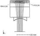
根据本发明的各种实施例,可以使用许多不同的方法将体光栅记录在波导单元中。可以使用任何数量和类型的电磁辐射源来实现光学元件在光学记录材料中的记录。取决于应用,(一个或多个)曝光源和/或记录系统可以被配置为使用变化的持续时间和曝光功率水平来记录光学元件。如以上关于SBG所讨论的,用于记录体光栅的技术可以包括光学记录材料的使用两个相互相干的激光波束的曝光,其中两个波束的叠加产生沿着干涉图案的周期性的强度分布。光学记录材料可以形成光栅结构,该光栅结构表现出与周期性强度分布匹配的折射率调制图案。在HPDLC混合物中,光强度分布导致单体扩散和聚合到高强度区域内,并且同时液晶扩散到暗区域内。这种相分离产生形成光栅的条纹平面的交替的富液晶区域和贫液晶区域。取决于如何配置记录波束,光栅结构可以被形成有倾斜的或非倾斜的条纹。图4A-图4D概念性地图示了根据本发明的各种实施例的两波束记录过程。如所示,两种方法可以用于产生两种不同类型的布拉格光栅—即,透射光栅400和反射光栅401。取决于如何定位两个记录波束402、403,干涉图案404可以将透射或是反射光栅记录在光学记录材料405中。可以在条纹的朝向上看到两种类型的光栅之间的差异(即,反射体光栅的条纹通常基本上平行于基板的表面,以及透射光栅的条纹通常基本上垂直于基板的表面)。在回放期间,入射在透射光栅400上的波束406可以导致被透射的衍射波束407。另一方面,入射在反射光栅401上的波束408可以导致被反射的波束409。According to various embodiments of the present invention, volume gratings can be recorded in the waveguide unit using a number of different methods. The recording of the optical element in the optical recording material can be accomplished using any number and type of electromagnetic radiation sources. Depending on the application, the exposure source(s) and/or recording system may be configured to record optical elements using varying durations and exposure power levels. As discussed above with respect to SBG, techniques for recording volume gratings may include exposure of the optical recording material using two mutually coherent laser beams, wherein the superposition of the two beams produces a periodic intensity distribution along the interference pattern. Optical recording materials can form grating structures that exhibit refractive index modulation patterns matched to periodic intensity distributions. In HPDLC mixtures, the light intensity distribution results in diffusion and polymerization of monomers into high intensity regions, and simultaneous diffusion of liquid crystals into dark regions. This phase separation produces alternating liquid crystal-rich and liquid-crystal-poor regions forming the fringe planes of the grating. Depending on how the recording beam is configured, the grating structure can be formed with slanted or non-slanted fringes. 4A-4D conceptually illustrate a two-beam recording process according to various embodiments of the present invention. As shown, two methods can be used to produce two different types of Bragg gratings—ie, transmission grating 400 and reflection grating 401 . Depending on how the two
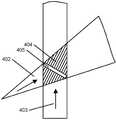
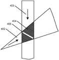
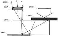
用于在光学记录材料中记录体光栅的另一种方法包括使用单个波束以在光学记录材料上形成干涉图案。这可以通过母版光栅的使用来实现。在许多实施例中,母版光栅是体光栅。在一些实施例中,母版光栅是振幅光栅。在与母版光栅相互作用后,单个波束可以衍射。一级衍射和零级波束可以重叠以产生干涉图案,该干涉图案然后可以曝光光学记录材料以形成期望的体光栅。在图5中概念性地图示了根据本发明的实施例的利用振幅光栅的单波束记录过程。如所示,来自单个激光源(未示出)的波束500被导引通过振幅光栅501。在与光栅501相互作用后,波束500可以衍射,像例如在光线与振幅光栅的黑色阴影区域相互作用的情况那样,或者波束500可以传播通过振幅光栅而没有实质性偏离,像例如在光线与振幅光栅的交叉窗口区域(cross-hatched region)相互作用的情况那样。一级衍射波束502和零级波束503可以重叠以产生干涉图案,该干涉图案曝光波导单元的光学记录层504。在说明性实施例中,间隔块505位于光栅501和光学记录层504之间,以便更改两个部件之间的距离。Another method for recording volume gratings in an optical recording material involves the use of a single beam to form an interference pattern on the optical recording material. This can be achieved through the use of a master raster. In many embodiments, the master grating is a volume grating. In some embodiments, the master grating is an amplitude grating. After interacting with the master grating, individual beams can be diffracted. The first-order diffracted and zero-order beams can overlap to create an interference pattern, which can then expose the optical recording material to form the desired volume grating. A single beam recording process utilizing an amplitude grating according to an embodiment of the present invention is conceptually illustrated in FIG. 5 . As shown,
虽然在图4A-图4D和图5中讨论并示出了记录体光栅的具体方法,但是根据本发明的各种实施例的记录系统可以被配置为实现用于记录体光栅的许多方法中的任何方法。Although specific methods of recording volume gratings are discussed and shown in FIGS. 4A-4D and 5, recording systems according to various embodiments of the present invention may be configured to implement any of the many methods for recording volume gratings any method.
滚动的K向量光栅和复用K向量光栅Rolled K-Vector Raster and Multiplexed K-Vector Raster
在解决体布拉格光栅中在其上发生衍射的范围有限的波长和角度方面,可以利用若干方法来增加光栅的衍射带宽。在许多实施例中,光栅可以采用关于它们的K向量变化的条纹。在许多实施例中,跨滚动的K向量的改变通常使得K向量中改变的方向不在具有波导或光栅元件的平面中。可以以许多不同的方式来实现变化的条纹或滚动的K向量。在一些实施例中,光栅的条纹被设计为在光栅上以渐进的方式变化。在其它实施例中,具有不同条纹的不同的分立的光栅集合被依次地放置。可以以各种方式来设计和配置具有滚动的K向量的光栅。在许多实施例中,滚动的K向量被设计为使得每个光栅部分的峰衍射效率针对其在那个位置处的对应的输出角被优化。在一些实施例中,每个光栅在不同位置处的峰衍射效率按照其在那个位置处的对应的输出角偏移。已示出了通过引入这个偏移,可以改善眼动范围的均匀性。在若干实施例中,与仅仅匹配在不同位置处的峰衍射效率相比,偏移可以将总图像亮度改善两倍。In addressing the limited range of wavelengths and angles over which diffraction occurs in a volume Bragg grating, several methods can be utilized to increase the diffraction bandwidth of the grating. In many embodiments, gratings may employ fringes that vary with respect to their K vector. In many embodiments, the change in the K vector across the roll is generally such that the direction of the change in the K vector is not in the plane with the waveguide or grating element. Varying stripes or rolling K-vectors can be implemented in many different ways. In some embodiments, the fringes of the grating are designed to vary in a progressive manner across the grating. In other embodiments, different discrete sets of gratings with different fringes are placed sequentially. A grating with rolling K-vectors can be designed and configured in various ways. In many embodiments, the rolling K vector is designed such that the peak diffraction efficiency of each grating section is optimized for its corresponding output angle at that location. In some embodiments, the peak diffraction efficiency of each grating at a different location is shifted by its corresponding output angle at that location. It has been shown that by introducing this offset, the uniformity of the eye movement range can be improved. In several embodiments, shifting can improve overall image brightness by a factor of two compared to just matching peak diffraction efficiencies at different locations.
根据本发明的实施例,滚动的K向量光栅可以用于最大化入耦合光的峰衍射效率。滚动的k向量的使用使得能够高效率输入耦合到光栅内,并且还允许优化波束扩展角以最小化波导的厚度;这可能需要平衡波导的厚度、光栅的角带宽以及场角的在光栅上任何给定点处的扩展。随着滚动K向量(并维持表面节距),光栅的低角度响应可以防止输出耦合,从而允许最小化波导厚度。在许多实施例中,设计目标是确保在某一点处的最大输入耦合并最小化角度分集,使得可以最小化光栅厚度而不会在不同点处互不耦合。According to embodiments of the present invention, a rolling K-vector grating can be used to maximize the peak diffraction efficiency of the in-coupled light. The use of rolling k-vectors enables high-efficiency in-coupling into the grating, and also allows optimization of the beam spread angle to minimize the thickness of the waveguide; this may require balancing the thickness of the waveguide, the angular bandwidth of the grating, and any variation in the field angle on the grating. expansion at a given point. As the K vector is rolled (and the surface pitch is maintained), the low angular response of the grating prevents outcoupling, allowing minimization of the waveguide thickness. In many embodiments, the design goal is to ensure maximum in-coupling at a certain point and minimize angular diversity so that grating thickness can be minimized without decoupling at different points.
图6A和图6B概念性地图示了根据本发明的各种实施例的滚动的K向量光栅的两种实施方式。首先参考图6A,在一些实施例中,滚动的K向量光栅可以被实现为包含具有不同K向量的分立的光栅元件600的波导部分。接下来参考图6B,在若干实施例中,滚动的K向量光栅可以被实现为包含光栅元件601的波导部分,在该光栅元件601内K向量经历方向上的平滑的单调变化。如所图示的,K向量的方向上的改变不在具有波导的平面中。6A and 6B conceptually illustrate two implementations of a rolling K-vector grating in accordance with various embodiments of the present invention. Referring first to FIG. 6A, in some embodiments, a rolling K-vector grating may be implemented as a waveguide section containing discrete
在许多实施例中,不同的分立条纹集合被叠加到同一光栅内,从而产生具有在同一体积内独立工作且彼此没有干扰的实质上多个光栅的复用光栅。例如,如果以相同的入射角针对两个不同的布拉格波长在同一设备中记录两个体光栅,那么该设备可以以有限的串扰将两个所选择的波长衍射到不同的输出方向内。复用可以用于通过组合两个相似方案(prescription)的光栅来产生改善的角度分布,以扩展衍射效率角带宽并给出跨出射光瞳和视场的更好的亮度均匀性和色彩平衡。复用还可以用于编码两个不同的衍射方案,该两个不同的衍射方案可以被设计为将光投射到不同的区域场内,或将两个不同波长的光衍射到给定的视场区域内。可以采取步骤以确保在记录期间没有光栅之间的导致不等的衍射效率和回放中光栅之间的串扰的竞争。复用还可以提供减少波导结构中的层数的显著优点。在一些实施例中,输入光栅、折叠光栅或输出光栅中的至少一个可以组合两个或更多个角衍射方案,以扩展角带宽。类似地,在若干实施例中,输入光栅、折叠光栅或输出光栅中的至少一个可以组合两个或更多个光谱衍射方案以扩展光谱带宽。例如,色彩复用光栅可以用于衍射两个或更多个基色(primary color)。In many embodiments, different sets of discrete fringes are superimposed into the same grating, resulting in a multiplexed grating with substantially multiple gratings operating independently within the same volume without interfering with each other. For example, if two volume gratings are recorded in the same device for two different Bragg wavelengths at the same angle of incidence, the device can diffract the two selected wavelengths into different output directions with limited crosstalk. Multiplexing can be used to produce an improved angular distribution by combining two gratings of similar prescription to expand the diffraction efficiency angular bandwidth and give better luminance uniformity and color balance across the exit pupil and field of view. Multiplexing can also be used to encode two different diffraction schemes that can be designed to project light into different area fields, or diffract two different wavelengths of light into a given field of view within the area. Steps can be taken to ensure that there is no competition between gratings during recording that results in unequal diffraction efficiencies and crosstalk between gratings in playback. Multiplexing can also provide significant advantages in reducing the number of layers in the waveguide structure. In some embodiments, at least one of the input grating, folded grating, or output grating may combine two or more angular diffraction schemes to expand the angular bandwidth. Similarly, in several embodiments, at least one of the input grating, folded grating, or output grating may combine two or more spectral diffraction schemes to expand the spectral bandwidth. For example, a color multiplexing grating can be used to diffract two or more primary colors.
图7概念性地图示了根据本发明的实施例的复用的K向量光栅。如所图示的,复用光栅700包含两个条纹集合701、702。第一集合701由实对角线描绘并且具有K向量K1和周期Λ1。第二复用光栅702由点划线图示并且具有K向量K2和周期Λ2。在图示的实施例中,两个光栅周期是相同的,但是K向量在方向上不同。在操作中,复用光栅701、702中的两者均是有源的并且可以提供更宽的入射和衍射带宽。复用光栅的入射角带宽θi覆盖包括重叠的θi1和θi2的角度范围。复用光栅701、702的衍射角带宽θd覆盖包括重叠的θd1和θd2的角度范围。在一些实施例中,多于两个光栅被复用。Figure 7 conceptually illustrates a multiplexed K-vector grating in accordance with an embodiment of the present invention. As illustrated, the multiplexed grating 700 includes two fringe sets 701 , 702 . The
虽然以上讨论了具有变化的条纹的具体光栅结构,但是根据给定应用的具体要求,可以利用许多条纹配置中的任何条纹配置。例如,如由制造限制所允许的,可以复用任何数量的光栅。滚动的K向量光栅可以被设计为具有以任何分立的单位滚动的K向量。While specific grating structures with varying fringes are discussed above, any of a number of fringe configurations may be utilized depending on the specific requirements of a given application. For example, any number of gratings may be multiplexed as permitted by manufacturing constraints. Rolled K-vector rasters can be designed to have K-vectors rolled in any discrete unit.
实现光瞳扩展的波导Waveguide for pupil expansion
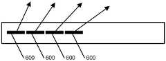
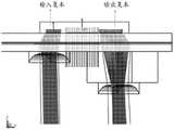
光栅可以以各种不同的方式被实现在波导中。在一些实施例中,光栅驻留在波导的外表面上。在其它实施例中,体光栅被实现在波导内部。光栅也可以被实现为执行不同的光学功能,诸如但不限于耦合光、导引光以及防止光的透射。图8概念性地图示了根据本发明的实施例的利用耦合光栅以将光衍射进和出波导的波导。如所示,波导800包括第一表面801,第二表面802、输入光栅元件803以及输出光栅元件804。来自投影透镜的准直光805以正交角通过第一表面801进入波导。光以其原始的角度行进通过波导800,并在到达波导800的另一侧处的第二表面802之前与输入光栅元件803相互作用。输入光栅元件803可以被设计为以倾斜的角度衍射光805,使得折射光806以可以发生全内反射的角度入射在第二表面802上。照此,光805被耦合到波导内并且被限制在波导800的第一表面801和第二表面802内。在说明性实施例中,光在波导800内行进,直到其与输出光栅804相互作用,该输出光栅804将光折射并耦合出波导800并进入用户的眼睛807。Gratings can be implemented in waveguides in a variety of different ways. In some embodiments, the grating resides on the outer surface of the waveguide. In other embodiments, the volume grating is implemented inside the waveguide. Gratings can also be implemented to perform different optical functions such as, but not limited to, coupling light, guiding light, and preventing transmission of light. 8 conceptually illustrates a waveguide utilizing a coupling grating to diffract light into and out of the waveguide in accordance with an embodiment of the present invention. As shown, the
在许多实施例中,衍射光栅可以通过有效地扩展准直光学系统的出射光瞳来用于在减小透镜尺寸的同时保持眼动范围的尺寸。出射光瞳可以被定义为虚拟孔径,其中只有穿过这个虚拟孔径的光线才可以进入用户的眼睛。图9和图10概念性地图示了根据本发明的实施例的利用输出光栅的波导,该输出光栅用于在一个维度上的出射光瞳扩展。图9中的波导900包括第一表面901、第二表面902、输入光栅元件903以及输出光栅元件904。如所示,光905通过输入光栅902耦合到波导900内,并且可以经由全内反射行进通过波导900。在说明性实施例中,输出光栅904被延展并被设计为折射被波导的光的一部分。光可以被折射使得折射光906以不发生全内反射的角度入射在第二表面902上,从而允许光906耦合出波导900。这种有损提取允许出射光瞳扩展,因为剩余的光可以继续在波导900内行进,并且一旦光再次入射在输出光栅904上,以上所描述的场景就可以再次发生。利用这种技术,还可以用恰当的设计来实现连续扩展的出射光瞳,如图10中所示。In many embodiments, diffraction gratings can be used to reduce the size of the lens while maintaining the size of the eye movement range by effectively expanding the exit pupil of the collimating optical system. The exit pupil can be defined as a virtual aperture where only light rays passing through this virtual aperture can enter the user's eye. 9 and 10 conceptually illustrate a waveguide utilizing an output grating for exit pupil expansion in one dimension, according to embodiments of the present invention. The
在图9和图10中的思想上扩展,光学波导可以被设计为在两个维度上扩展出射光瞳。在许多实施例中,两个波导可以被堆叠在一起以产生系统,在该系统中耦合到波导堆叠内的光可以实现在两个维度上的出射光瞳扩展。图11概念性地图示了根据本发明的实施例的利用两个平面波导以提供在两个维度上的出射光瞳扩展的波导系统。如所示,系统1100包括第一波导1101和第二波导1102。第一波导1101可以包括第一输入耦合光栅1103和第一输出耦合光栅1104,以及第二波导1102可以包括第二输入耦合光栅1105和第二输出耦合光栅1106。第一输入耦合光栅1103可以被设计为将来自图像源1108的准直光1107耦合到第一波导1101内。类似于图9和图10中所描述的系统,被限制的光可以经由全内反射行进通过第一波导1101,直到光到达第一输出耦合光栅1104。在说明性实施例中,第一输出耦合光栅1104被设计为提供在第一维度上的有损的出射光瞳扩展,并且将光耦合出第一波导1101。第二输入耦合光栅1105可以被设计为接收从第一波导1101输出的在第一维度上扩展的光,并且折射接收到的光,使得接收到的光经由全内反射行进通过第二波导1102。在许多实施例中,第一输出耦合光栅1104和第二输入耦合光栅1106以类似的方式延展。然后,行进通过第二波导1102的光可以与第二输出耦合光栅1106相互作用。在说明性实施例中,第二输出耦合光栅1106被设计为提供在不同于第一维度的第二维度上的有损的出射光瞳扩展,并且将光耦合出第二波导1102。作为结果,出射光瞳在两个维度上扩展,从而允许关于眼动范围尺寸1109更小的透镜尺寸。Expanding on the ideas in Figures 9 and 10, optical waveguides can be designed to expand the exit pupil in two dimensions. In many embodiments, two waveguides can be stacked together to create a system in which light coupled into the waveguide stack can achieve exit pupil expansion in two dimensions. 11 conceptually illustrates a waveguide system utilizing two planar waveguides to provide exit pupil expansion in two dimensions in accordance with an embodiment of the present invention. As shown, the
在许多实施例中,光学波导利用折叠光栅,该折叠光栅可以在波导内导引光的同时提供在一个维度上的出射光瞳扩展。在进一步的实施例中,折叠光栅导引光朝向输出光栅,该输出光栅可以提供在不同于第一方向的第二维度上的出射光瞳扩展,并且还将光耦合出波导。通过使用折叠光栅,与其它显示信息的系统和方法相比,波导显示器可以要求更少的层。此外,通过使用折叠光栅,光可以通过波导内的全内反射在由波导外表面定义的单个矩形棱镜中行进,同时实现双光瞳扩展。作为结果,可以使用单个波导来实现二维的出射光瞳扩展。图12概念性地图示了根据本发明的实施例的利用三光栅结构以提供二维的出射光瞳扩展的波导。如所示,波导1200包括输入光栅1201、折叠光栅1202以及输出光栅1203。光栅1201-1203上的箭头1204-1206示出了与每个光栅相关联的k向量。在许多实施例中,折叠光栅1202可以被设计为提供在一个维度上的出射光瞳扩展,并重新导引来自输入光栅1201的经由全内反射传播的光的方向。在说明性实施例中,折叠光栅1202的条纹与其它两个光栅1201、1203中的任一个成45度偏移。入射在折叠光栅上的光1207被重新导引到1208,以朝向输出光栅1203传播,该输出光栅1203提供了在第二维度上的出射光瞳扩展并将光耦合出波导1200。In many embodiments, the optical waveguide utilizes a folded grating that can provide exit pupil expansion in one dimension while guiding light within the waveguide. In a further embodiment, the folded grating directs light towards an output grating that can provide exit pupil expansion in a second dimension different from the first direction and also couples light out of the waveguide. By using folded gratings, waveguide displays can require fewer layers than other systems and methods of displaying information. Furthermore, by using folded gratings, light can travel in a single rectangular prism defined by the outer surface of the waveguide through total internal reflection within the waveguide, while achieving dual pupil expansion. As a result, a two-dimensional exit pupil expansion can be achieved using a single waveguide. Figure 12 conceptually illustrates a waveguide utilizing a triple grating structure to provide a two-dimensional exit pupil expansion according to an embodiment of the present invention. As shown,
虽然以上与图8-图12有关的讨论描述了具体的波导结构,但是容易认识到的是,根据给定应用的具体要求,可以利用任何数量的波导结构配置。例如,提供出射光瞳扩展的光栅可以被设计为具有梯度效率(gradient efficiency),使得折射光的一部分取决于入射的区域而变化。While the above discussion in relation to FIGS. 8-12 describes specific waveguide structures, it is readily recognized that any number of waveguide structure configurations may be utilized depending on the specific requirements of a given application. For example, a grating that provides exit pupil expansion can be designed to have gradient efficiency, such that a portion of the refracted light varies depending on the region of incidence.
波导层堆叠Waveguide Layer Stacking
根据本发明的各种实施例的波导可以被堆叠在一起以实现某些光学功能。例如,在许多实施例中,设备可以包括RGB衍射层堆叠,每个层包括输入光栅和输出光栅。在每个层中SBG被记录以提供相对于(沿着波导)从峰波长偏移小增量的波长特点的峰衍射效率。在一些实施例中,RGB SBG层被使用并且可以与RGB LED图像源顺序地和同步地开关。图13概念性地图示了根据本发明的实施例的波导1300的RGB堆叠的剖面视图。在说明性实施例中,波长选择性吸收层1301-1303被用于选择性地吸收每个波导层1304-1306中的不想要的光。虚线表示由于偏振失配或是布拉格失配引起的弱耦合。波导的堆叠还包括各种滤光器和波片1307-1311。偏振朝向是关于输入光栅描绘的。Waveguides according to various embodiments of the present invention may be stacked together to achieve certain optical functions. For example, in many embodiments, a device may include a stack of RGB diffractive layers, each layer including an input grating and an output grating. SBGs are recorded in each layer to provide peak diffraction efficiencies relative to wavelength characteristics that are shifted (along the waveguide) in small increments from the peak wavelength. In some embodiments, an RGB SBG layer is used and can be switched on and off sequentially and synchronously with the RGB LED image source. 13 conceptually illustrates a cross-sectional view of an RGB stack of
虽然图13图示了波导堆叠的具体结构,但是根据给定应用的具体要求,可以使用许多堆叠配置中的任何堆叠配置。例如,在许多实施例中,仅红以及蓝/绿两层被用于实现RGB堆叠。可以使用若干方法来实现这样的系统。在一些实施例中,包含各自与RGB色彩相关的不同的光栅集合的复用光栅被用于实现一个波导层中的多个色彩波导。Although Figure 13 illustrates the specific structure of a waveguide stack, any of a number of stack configurations may be used depending on the specific requirements of a given application. For example, in many embodiments, only red and blue/green layers are used to implement RGB stacking. Such a system can be implemented using several methods. In some embodiments, multiplexed gratings containing distinct sets of gratings each associated with RGB colors are used to implement multiple color waveguides in one waveguide layer.
波导显示器waveguide display
可以以许多不同的方式来实现和约束根据本发明的各种实施例的波导显示器。例如,波导显示器可以包含变化数量的波导层和不同的出射光瞳扩展方案。图14概念性地图示了根据本发明的实施例的具有两个光栅层的双轴扩展波导显示器。如所示,波导显示器1400包括光源1401、微显示面板1402和光学地耦合到具有两个光栅层的波导1404的输入图像节点(“IIN”)1403。在一些实施例中,通过将光栅层夹在玻璃或塑料基板之间以形成堆叠来形成波导,在该堆叠内,全内反射发生在外基板和空气界面处。在若干实施例中,堆叠还可以包括附加层,诸如分束涂层和环境保护层。在说明性实施例中,每个光栅层包含输入光栅1405A、1405B,折叠光栅出射光瞳扩展器1406A、1406B以及输出光栅1407A、1407B,其中字符A和B分别指第一波导层和第二波导层。输入光栅、折叠光栅以及输出光栅可以是全息光栅,诸如可开关或不可开关的SBG。如本文所使用的,术语光栅可以涵盖可以包括光栅集合的光栅,诸如复用光栅或分立的滚动K向量光栅的集合。在说明性实施例中,IIN 1403集成了微显示面板1402、光源1401,以及照亮显示面板、分开反射光以及将其准直到需要的FOV内所需的光学部件。在图14的实施例中以及在以下要描述的实施例中,输入光栅、折叠光栅和输出光栅中的至少一个可以是电可开关的。在许多实施例中,所有三种光栅类型都是无源的(即,非开关的)。在许多实施例中,IIN可以投射被显示在微显示面板上的图像,使得每个显示像素被转换成基板波导内的独特的角方向。IIN中所包含的准直光学器件可以包括透镜和反射镜。在进一步的实施例中,透镜和反射镜是衍射透镜和反射镜。Waveguide displays according to various embodiments of the present invention can be implemented and constrained in many different ways. For example, a waveguide display may contain varying numbers of waveguide layers and different exit pupil expansion schemes. Figure 14 conceptually illustrates a biaxial extended waveguide display with two grating layers in accordance with an embodiment of the present invention. As shown, the
在说明性实施例中,从源经由IIN到波导的光路由光线1408-1411指示。每个光栅层的输入光栅1405A、1405B可以将光的一部分耦合到波导1404中的TIR路径内,这样的路径由光线1412、1413表示。输出光栅1407A、1407B可以将光从波导衍射到准直光1414、1415的角度范围内,用于被眼睛1416观看。可以通过IIN光学器件定义与显示器的视场对应的角范围。在一些实施例中,波导光栅可以编码用于调整输出的准直的光学功率。在一些实施例中,输出图像在无限远处。在其它实施例中,输出图像可以被形成在距眼动范围若干米的距离处。通常,眼睛位于显示器的眼动范围或出射光瞳内。In the illustrative embodiment, the optical route from the source to the waveguide via IIN is indicated by light rays 1408-1411. The
可以如标题为“Holographic Wide Angle Display”的美国专利申请No.13/869,866和标题为“Transparent Waveguide Display”的美国专利申请No.13/844,456中所讨论和教导的那样利用不同的IIN实施方式和实施例,这些申请的公开内容通过引用整体合并于此。在一些实施例中,IIN包含用于将光导引到微显示器上以及朝向波导传输反射光的分束器。在许多实施例中,分束器是被记录在HPDLC中的光栅,并且使用这样的光栅的固有的偏振选择性来分开照亮显示器的光和从显示器反射的图像调制光。在若干实施例中,分束器是偏振分束器块(polarizing beam splitter cube)。在许多实施例中,IIN结合去散斑器(despeckler)。在标题为“Laser Illumination Device”的美国专利No.8,565,560中讨论了去散斑器,该专利的公开内容通过引用整体合并于此。Various IIN implementations and methods can be utilized as discussed and taught in US Patent Application No. 13/869,866 entitled "Holographic Wide Angle Display" and US Patent Application No. 13/844,456 entitled "Transparent Waveguide Display". Examples, the disclosures of these applications are hereby incorporated by reference in their entirety. In some embodiments, the IIN includes a beam splitter for directing light onto the microdisplay and transmitting the reflected light towards the waveguide. In many embodiments, the beam splitter is a grating recorded in the HPDLC, and the inherent polarization selectivity of such a grating is used to separate the light illuminating the display and the image-modulated light reflected from the display. In several embodiments, the beam splitter is a polarizing beam splitter cube. In many embodiments, the IIN incorporates a despeckler. De-specklers are discussed in US Patent No. 8,565,560, entitled "Laser Illumination Device," the disclosure of which is incorporated herein by reference in its entirety.
光源可以是激光器或LED,并且可以包括用于修改照明波束角特点的一个或多个透镜。图像源可以是微显示器或基于激光的显示器。LED可以提供比激光器更好的均匀性。如果使用激光照明,那么存在在波导输出处出现照明带的风险。在许多实施例中,可以使用在标题为“Method and Apparatus for Generating Input Images for HolographicWaveguide Displays”的美国专利申请No.15/512,500中公开的技术和教导来克服波导中的激光照明带,该申请的公开内容通过引用整体合并于此。在一些实施例中,来自光源的光被偏振。在若干实施例中,图像源是液晶显示器(LCD)微显示器或硅上液晶(LCoS)微显示器。The light source may be a laser or LED, and may include one or more lenses for modifying the angular characteristics of the illumination beam. The image source can be a microdisplay or a laser-based display. LEDs can provide better uniformity than lasers. If laser illumination is used, there is a risk of an illumination band appearing at the waveguide output. In many embodiments, the techniques and teachings disclosed in US Patent Application No. 15/512,500, entitled "Method and Apparatus for Generating Input Images for Holographic Waveguide Displays," can be used to overcome laser-illuminated strips in waveguides, which The disclosure is incorporated herein by reference in its entirety. In some embodiments, the light from the light source is polarized. In several embodiments, the image source is a liquid crystal display (LCD) microdisplay or a liquid crystal on silicon (LCoS) microdisplay.
在一些实施例中,类似于图14中示出的光栅层,每个光栅层解决总视场的一半。通常,折叠光栅被以45度记录(clocked)(即,在波导平面中偏斜),以确保折叠光的足够的角带宽。在其它实施例中,其它记录角(clock angle)可以用于满足在显示器的人体工程学设计中可能出现的对光栅定位的空间约束。在一些实施例中,输入光栅和输出光栅中的至少一个具有滚动的k向量。滚动K向量可以允许光栅的角带宽被扩展而无需增加波导厚度。In some embodiments, similar to the grating layers shown in Figure 14, each grating layer addresses half of the total field of view. Typically, folded gratings are clocked (ie, skewed in the waveguide plane) at 45 degrees to ensure sufficient angular bandwidth of the folded light. In other embodiments, other clock angles may be used to meet spatial constraints on grating positioning that may arise in the ergonomic design of the display. In some embodiments, at least one of the input raster and the output raster has a rolling k-vector. Rolling the K vector can allow the angular bandwidth of the grating to be expanded without increasing the waveguide thickness.
在许多实施例中,可以通过设计光栅方案来提供被引导的光与光栅的双重相互作用,以增强折叠光栅的角带宽。在标题为“Waveguide Grating Device”的美国专利申请No.:14/620,969中公开了双重相互作用折叠光栅的示例性实施例,该申请的公开内容整体合并于此。In many embodiments, the grating scheme can be designed to provide dual interaction of the guided light with the grating to enhance the angular bandwidth of the folded grating. Exemplary embodiments of dual interacting folded gratings are disclosed in US Patent Application No.: 14/620,969, entitled "Waveguide Grating Device," the disclosure of which is incorporated herein in its entirety.
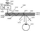
图15概念性地图示了根据本发明的实施例的类似于图14中所使用的单个光栅层的平面视图1500。光学地耦合到IIN 1502的光栅层1501包括输入光栅1503、第一分束器1504、折叠光栅1505、第二分束器1506以及输出光栅1507。分束器可以是部分透射涂层,其通过提供在波导内的多条反射路径来使被波导的光均匀化。每个分束器可以包括多于一个涂层,其中每个涂层都被施加到透明基板。从IIN上止眼睛1508的典型的波束路径由光线1509-1513指示。Figure 15 conceptually illustrates a
图16概念性地图示了根据本发明的实施例的两个光栅层配置的平面视图1600。如所示,光学地耦合到IIN 1602的光栅层1601A、1601B包括输入光栅1603A、1603B,第一分束器1604A、1604B,折叠光栅1605A、1605B,第二分束器1606A、1606B以及输出光栅1607A、1607B,其中字符A、B分别指第一光栅层和第二光栅层。在图示的实施例中,两层光栅和分束器基本上重叠。16 conceptually illustrates a plan view 1600 of a two grating layer configuration in accordance with an embodiment of the present invention. As shown, grating layers 1601A, 1601B optically coupled to
在许多实施例中,光栅层可以被分解成分开的层。例如,在一些实施例中,第一层包括折叠光栅,而第二层包括输出光栅。在进一步的实施例中,第三层可以包括输入光栅。在这样的实施例中,然后,这许多层可以被层压在一起成为单个波导基板。在若干实施例中,光栅层包括许多片,包括被层压在一起以形成单个基板波导的输入耦合器、折叠光栅以及输出光栅(或其部分)。这些片可以被光学胶或折射率与这些片的折射率相匹配或基本上相似的其它透明材料分隔。In many embodiments, the grating layer may be decomposed into separate layers. For example, in some embodiments, the first layer includes a folded grating and the second layer includes an output grating. In further embodiments, the third layer may include an input grating. In such an embodiment, the many layers may then be laminated together into a single waveguide substrate. In several embodiments, the grating layer includes a number of sheets, including an input coupler, a folded grating, and an output grating (or portions thereof) that are laminated together to form a single substrate waveguide. The sheets may be separated by optical glue or other transparent material having an index of refraction that matches or is substantially similar to that of the sheets.
在许多实施例中,光栅层可以经由单元制作过程通过产生期望光栅厚度的单元并且对于输入耦合器、折叠光栅以及输出光栅中的每个用SBG材料真空填充每个单元来形成。在一些实施例中,可以通过定位具有在玻璃板之间的间隙的多个玻璃板来形成单元,该玻璃板之间的间隙定义了输入耦合器、折叠光栅以及输出光栅的期望的光栅厚度。在若干实施例中,一个单元可以由多个孔径制成,使得不同的孔径被用不同的SBG材料袋填充。然后,任何介于中间的空间可以被分隔材料(例如,胶、油等)分隔,以定义分隔区域。在许多实施例中,SBG材料可以被旋涂到基板上,并且然后在材料固化之后被第二基板覆盖。In many embodiments, the grating layer may be formed via a cell fabrication process by creating cells of the desired grating thickness and vacuum filling each cell with SBG material for each of the input coupler, folded grating, and output grating. In some embodiments, the cell may be formed by positioning multiple glass sheets with gaps between the glass sheets that define the desired grating thickness of the input coupler, folded grating, and output grating. In several embodiments, a cell may be made of multiple apertures such that different apertures are filled with different bags of SBG material. Any intervening spaces can then be separated by a separation material (eg, glue, oil, etc.) to define separation regions. In many embodiments, the SBG material can be spin-coated onto a substrate and then covered by a second substrate after the material is cured.
在许多实施例中,可以通过干涉在基板内的一定角度处的两个光波以产生全息波前来产生输入耦合器、折叠光栅和输出光栅,从而在波导基板中产生以期望的角度设置的亮条纹和暗条纹。此外,还可以使用以上各部分中所描述的各种方法中的任何方法来制造这样的光学元件。In many embodiments, the input coupler, folded grating, and output grating can be generated by interfering two light waves at an angle within the substrate to produce a holographic wavefront, thereby producing a bright setting in a waveguide substrate at a desired angle Stripes and dark stripes. Furthermore, such optical elements may also be fabricated using any of the various methods described in the sections above.
在一个实施例中,被实施为SBG的输入耦合器、折叠光栅以及输出光栅可以是被记录在全息聚合物分散的液晶(HPDLC)(例如,液晶微滴的基体)中的布拉格光栅,尽管也可以将SBG记录在其它材料中。在一个实施例中,SBG被记录在均匀调制材料中,诸如具有分散在液态聚合物中的固态液晶的基体(matrix)的POLICRYPS或POLIPHEM。SBG本质上可以是开关的或非开关的。在其非开关形式中,由于其液晶成分,SBG具有优于常规全息感光聚合物材料的优点,其能够提供高折射率调制。示例性的均匀调制液晶聚合物材料系统在Caputo等人的美国专利申请公开No.:US2007/0019152和Stumpe等人的PCT申请No.:PCT/EP2005/006950中公开,这些申请均通过引用整体并入本文。均匀调制光栅的特征在于高折射率调制(并且因此高衍射效率)和低散射。In one embodiment, the input coupler, folded grating, and output grating implemented as SBGs may be Bragg gratings recorded in holographic polymer dispersed liquid crystal (HPDLC) (eg, the matrix of liquid crystal droplets), although also SBGs can be recorded in other materials. In one embodiment, the SBG is recorded in a uniform modulation material, such as POLICRYPS or POLIPHEM with a matrix of solid liquid crystals dispersed in a liquid polymer. SBGs can be switched or non-switched in nature. In its non-switching form, due to its liquid crystal composition, SBG has advantages over conventional holographic photopolymer materials, which can provide high refractive index modulation. Exemplary uniformly modulated liquid crystal polymer material systems are disclosed in U.S. Patent Application Publication No.: US2007/0019152 to Caputo et al. and PCT Application No.: PCT/EP2005/006950 to Stumpe et al., which are incorporated by reference in their entirety. into this article. Uniformly modulated gratings are characterized by high refractive index modulation (and thus high diffraction efficiency) and low scattering.
在许多实施例中,输入耦合器、折叠光栅和输出光栅由反向模式HPDLC材料制成。反向模式HPDLC与常规HPDLC的不同在于,当没有施加电场时光栅是无源的,以及在电场的存在下光栅变成衍射的。反向模式HPDLC可以基于标题为“Improvements to HolographicPolymer Dispersed Liquid Crystal Materials and Devices”的PCT申请No.PCT/GB2012/000680中公开的任何配方和过程,该申请的公开内容整体合并于此。光栅可以被记录在以上材料系统中的任何材料系统中,但是以无源(非开关)模式被使用。制造过程与用于开关式的制造过程相同,但其中省略了电极涂覆阶段。鉴于它们的高折射率调制,LC聚合物材料系统是高度理想的。在一些实施例中,光栅被记录在HPDLC中,但不是开关式的。In many embodiments, the input coupler, folded grating, and output grating are made of reverse mode HPDLC material. Reverse mode HPDLC differs from conventional HPDLC in that the grating is passive when no electric field is applied, and that the grating becomes diffractive in the presence of an electric field. The reverse mode HPDLC can be based on any of the formulations and processes disclosed in PCT Application No. PCT/GB2012/000680 entitled "Improvements to Holographic Polymer Dispersed Liquid Crystal Materials and Devices", the disclosure of which is incorporated herein in its entirety. The grating can be recorded in any of the above material systems, but is used in passive (non-switching) mode. The manufacturing process is the same as that used for the switch mode, but where the electrode coating stage is omitted. Given their high refractive index modulation, LC polymer material systems are highly desirable. In some embodiments, the grating is recorded in HPDLC, but not switched.
在许多实施例中,输入光栅可以被另一种类型的输入耦合器代替,诸如但不限于棱镜和反射表面。在一些实施例中,输入耦合器可以是全息光栅,诸如SBG光栅或无源光栅,其可以是无源SBG光栅。输入耦合器可以被配置为接收来自显示源的准直光,并经由第一表面和第二表面之间的全内反射使光在波导内行进到折叠光栅。输入耦合器可以直接朝向折叠光栅或相对于折叠光栅以一定角度取向。例如,在若干实施例中,输入耦合器可以关于折叠光栅被设置成稍微倾斜。在许多实施例中,折叠光栅可以在对角线方向上取向。折叠光栅可以被配置为提供在第一方向上的光瞳扩展,并且经由波导内部的全内反射将光导引到输出光栅。In many embodiments, the input grating may be replaced by another type of input coupler, such as, but not limited to, prisms and reflective surfaces. In some embodiments, the input coupler may be a holographic grating, such as an SBG grating or a passive grating, which may be a passive SBG grating. The input coupler may be configured to receive collimated light from the display source and to travel the light within the waveguide to the folded grating via total internal reflection between the first surface and the second surface. The input coupler can be oriented directly towards the folded grating or at an angle relative to the folded grating. For example, in several embodiments, the input coupler may be positioned slightly inclined with respect to the folded grating. In many embodiments, the folded gratings may be oriented in a diagonal direction. The folded grating may be configured to provide pupil expansion in the first direction and to direct light to the output grating via total internal reflection inside the waveguide.
在许多实施例中,每个折叠光栅的纵向边缘斜交于输入耦合器的对准轴,使得每个折叠光栅关于显示光的传播方向被设置在对角线上。折叠光栅可以成一定角度,使得来自输入耦合器的光被重新导引到输出光栅。在一些实施例中,折叠光栅被设置为关于从输入耦合器释放的显示图像的方向成四十五度角。这个特征可以使沿着折叠光栅传播的显示图像被转到输出光栅内。例如,在若干实施例中,折叠光栅可以使图像转90度进入输出光栅。以这种方式,单个波导可以提供在水平方向和垂直方向两者上的双轴光瞳扩展。在许多实施例中,每个折叠光栅可以具有部分衍射结构。在一些实施例中,每个折叠光栅可以具有全衍射结构。In many embodiments, the longitudinal edge of each folded grating is oblique to the alignment axis of the input coupler such that each folded grating is positioned diagonally with respect to the direction of propagation of the display light. The folded grating can be angled so that light from the input coupler is redirected to the output grating. In some embodiments, the folded grating is positioned at a forty-five degree angle with respect to the direction of the display image released from the input coupler. This feature enables the display image propagating along the folded raster to be turned into the output raster. For example, in several embodiments, folding the raster can turn the image 90 degrees into the output raster. In this way, a single waveguide can provide biaxial pupil expansion in both horizontal and vertical directions. In many embodiments, each folded grating may have a partially diffractive structure. In some embodiments, each folded grating may have a fully diffractive structure.
输出光栅可以被配置为提供在不同于第一方向的第二方向上的光瞳扩展,并且使光从第一表面或第二表面离开波导。输出光栅可以经由全内反射接收来自折叠光栅的显示图像,并且可以提供在第二方向上的光瞳扩展。在许多实施例中,输出光栅包括多层基板,从而包括多层输出光栅。相应地,没有要求光栅在波导内的一个平面中,并且光栅可以被堆叠在彼此之上(例如,光栅的单元被堆叠在彼此之上)。The output grating may be configured to provide pupil expansion in a second direction different from the first direction and to cause light to exit the waveguide from either the first surface or the second surface. The output grating can receive the display image from the folded grating via total internal reflection and can provide pupil expansion in the second direction. In many embodiments, the output grating comprises a multilayer substrate, thereby comprising a multilayer output grating. Accordingly, the gratings are not required to be in one plane within the waveguide, and the gratings can be stacked on top of each other (eg, the elements of the gratings are stacked on top of each other).
在许多实施例中,基板波导上的四分之一波片旋转光线的偏振以维持与SBG的高效耦合。四分之一波片可以被耦合到或附接到基板波导的表面。例如,在一些实施例中,四分之一波片是施加到基板波导的涂层。四分之一波片可以提供光波偏振管理。这样的偏振管理可以通过补偿波导中的斜波(skew wave)来帮助光线保持与预期观察轴的对准。四分之一波片是可选的,并且可以增大实施方式中光学设计的效率。在若干实施例中,波导不包括四分之一波片。四分之一波片可以被提供为多层涂层。In many embodiments, a quarter wave plate on the substrate waveguide rotates the polarization of the light to maintain efficient coupling with the SBG. A quarter wave plate can be coupled or attached to the surface of the substrate waveguide. For example, in some embodiments, a quarter wave plate is a coating applied to a substrate waveguide. Quarter wave plates can provide light wave polarization management. Such polarization management can help keep the light aligned with the intended viewing axis by compensating for skew waves in the waveguide. A quarter wave plate is optional and can increase the efficiency of the optical design in embodiments. In several embodiments, the waveguide does not include a quarter wave plate. Quarter wave plates can be provided as multi-layer coatings.
在许多实施例中,波导显示器可以单色操作。在一些实施例中,波导显示器可以彩色操作。可以使用与图14的相似设计的单色波导的堆叠来实现彩色操作。该设计可以使用如所示的红波导层、绿波导层以及蓝波导层,或者可替代地使用红层以及蓝/绿层。图17概念性地图示了根据本发明的实施例的双轴扩展波导显示器1700,该双轴扩展波导显示器1700包括光源1701、微显示面板1702,以及光学地耦合到红波导1704R、绿波导1704G以及蓝波导1704B的IIN 1703,其中每个波导包括两个光栅层。在说明性实施例中,三个波导被气隙分隔。在一些实施例中,波导被诸如纳米多孔膜之类的低折射率材料分隔。如所示,用R标记的红光栅层包括输入光栅1705R、1706R,折叠光栅出射光瞳扩展器1707R、1708R以及输出光栅1709R、1710R。使用相同的编号标记蓝波导和绿波导的光栅元件,其中B、G指示蓝和绿。在一些实施例中,输入光栅、折叠光栅和输出光栅都是无源的,即,非开关的。在若干实施例中,光栅中的至少一个光栅是开关的。在许多实施例中,每层中的输入光栅是可开关的,以避免波导层之间的色彩串扰。在许多实施例中,可以通过在红波导和蓝波导以及蓝波导和绿波导的输入光栅区域之间布置二向色滤光器1711、1712来避免色彩串扰。在各种实施例中,可以在每个单色波导中使用仅一个光栅层来实现彩色波导。In many embodiments, the waveguide display can operate in monochrome. In some embodiments, the waveguide display can operate in color. Color operation can be achieved using a stack of monochromatic waveguides of a similar design to that of FIG. 14 . The design may use red, green, and blue waveguide layers as shown, or alternatively, red and blue/green layers. 17 conceptually illustrates a dual-axis
图18概念性地图示了根据本发明的实施例的眼动跟踪显示器。在标题为“Holographic Waveguide Eye Tracker”的PCT申请No.PCT/GB2014/000197、标题为“Holographic Waveguide Optical Tracker”的PCT申请No.PCT/GB2015/000274以及标题为“Apparatus for Eye Tracking”的PCT申请No.PCT/GB2013/000210中讨论了基于波导设备的眼动跟踪器,这些申请的公开内容整体合并于此。再次转到图18,眼动跟踪显示器1800包括基于以上所描述的任何实施例的双轴扩展波导显示器。波导显示器可以包括:包含结合了输入折叠和输出光栅的至少一个光栅层的波导1801,IIN 1802,包括波导的眼动跟踪器1803,红外检测器1804以及红外源1805。眼动跟踪器和显示波导可以被气隙或被低折射材料分隔。如在以上参考文献中所解释的,眼动跟踪器可以包括分开的照明和检测器波导。在说明性实施例中,从红外源到眼睛的光路由光线1806-1808指示,并且从眼睛反向散射的信号由光线1809、1810指示。从输入图像节点通过显示波导到眼动范围的光路由光线1811-1813指示。18 conceptually illustrates an eye-tracking display according to an embodiment of the present invention. In PCT Application No. PCT/GB2014/000197 entitled "Holographic Waveguide Eye Tracker", PCT Application No. PCT/GB2015/000274 entitled "Holographic Waveguide Optical Tracker" and PCT Application No. PCT/GB2015/000274 entitled "Apparatus for Eye Tracking" Waveguide device-based eye trackers are discussed in No. PCT/GB2013/000210, the disclosures of which are incorporated herein in their entirety. Turning again to FIG. 18, an eye-
在许多实施例中,双扩展波导显示器还可以包括动态聚焦元件。图19概念性地图示了根据本发明的实施例的双扩展波导显示器1900,该双扩展波导显示器1900具有布置在波导显示器的主表面附近的动态聚焦元件1901和眼动跟踪器。在一些实施例中,动态聚焦元件是LC设备。在若干实施例中,LC设备将LC层与衍射光学元件组合。在许多实施例中,衍射光学元件是电可控的基于LC的设备。在各种实施例中,动态聚焦元件被布置在波导显示器和眼动跟踪器之间。在各种实施例中,动态聚焦元件可以被布置在离眼睛最远的显示波导的表面附近。In many embodiments, the dual extended waveguide display may also include dynamic focusing elements. Figure 19 conceptually illustrates a dual
动态聚焦设备可以提供多重图像表面1902。在光场显示应用中,可以使用至少四个图像表面。动态聚焦元件可以基于在标题为“Electrically Focus Tunable Lens”的美国专利申请No.:15/553,120中所描述的动态聚焦元件,该申请的公开内容整体合并于此。在一些实施例中,具有动态聚焦元件和眼动跟踪器的双扩展波导显示器可以提供光场显示,诸如基于在标题为“Holographic Waveguide Light Field Displays”的美国专利申请No.15/543,013中公开的教导的那些,该申请的公开内容通过引用整体合并于此。A dynamic focus device may provide multiple image surfaces 1902. In light field display applications, at least four image surfaces can be used. The dynamic focusing element may be based on the dynamic focusing element described in US Patent Application No.: 15/553,120 entitled "Electrically Focus Tunable Lens," the disclosure of which is incorporated herein in its entirety. In some embodiments, dual extended waveguide displays with dynamic focusing elements and eye trackers can provide light field displays, such as those based on those disclosed in US Patent Application No. 15/543,013 entitled "Holographic Waveguide Light Field Displays" For those taught, the disclosure of this application is hereby incorporated by reference in its entirety.
虽然以上讨论了具体的波导结构,但是可以取决于给定应用的具体要求来实现许多波导结构中的任何波导结构。例如,在许多波导配置中,输入光栅、折叠光栅和输出光栅被形成在夹在透明基板之间的单个层中。这样的配置在图14中示出,其中两层照此被堆叠。在一些实施例中,波导包括仅仅一个光栅层。在若干实施例中,将开关透明电极施加到将开关光栅夹在中间的基板层的相对表面上。在许多实施例中,单元基板可以由玻璃制成。可以使用的一种玻璃基板是标准的康宁柳木(Corning Willow)玻璃基板(折射率1.51),其厚度可低至50微米。在其它实施例中,单元基板可以是光学塑料。Although specific waveguide structures are discussed above, any of a number of waveguide structures may be implemented depending on the specific requirements of a given application. For example, in many waveguide configurations, the input grating, folded grating, and output grating are formed in a single layer sandwiched between transparent substrates. Such a configuration is shown in Figure 14, where the two layers are stacked as such. In some embodiments, the waveguide includes only one grating layer. In several embodiments, switching transparent electrodes are applied to opposing surfaces of a substrate layer sandwiching the switching grating. In many embodiments, the cell substrate may be made of glass. One glass substrate that can be used is a standard Corning Willow glass substrate (refractive index 1.51), which can be as low as 50 microns thick. In other embodiments, the unit substrate may be optical plastic.
在许多实施例中,波导显示器通过光-机械接口耦合到IIN,该光-机械接口允许波导容易地从IIN组件收回。基本原理被概念性地图示在图20A中。图20A示出了双轴扩展波导显示器2000,该双轴扩展波导显示器2000包括波导2001以及IIN2005,该波导2001包含输入光栅2002、折叠光栅2003、输出光栅2004。该装置还包括连接到波导的光学链路2006、终止光学链路的第一光学接口2007,以及形成IIN的出射光学端口的第二光学接口2008。第一光学接口和第二光学接口可以如由图20B中所示的间隙2009所指示的被解耦。在一些实施例中,光学链路是波导。在若干实施例中,光学链路是弯曲的。在许多实施例中,光学链路是GRIN图像中继设备。在各种实施例中,使用机械机构来建立光学连接。在一些实施例中,光学连接是使用磁性机构来建立的。在头盔安装的显示器应用中,将波导从IIN解耦的优点在于,当不用时可以将显示器的近眼部分移开。在其中波导包括无源光栅的一些实施例中,近眼光学器件可以是可任意处理的。In many embodiments, the waveguide display is coupled to the IIN through an opto-mechanical interface that allows the waveguide to be easily retracted from the IIN assembly. The basic principle is conceptually illustrated in Figure 20A. FIG. 20A shows a dual-axis
图21概念性地图示了根据本发明的实施例的具有微显示面板2101、空间变化的NA部件2102以及微显示光学器件2103的IIN 2100。如所示,微显示光学器件2103接受来自照明源(未显示)的光2104,并在由光线2105指示的方向上将该光偏斜到微显示器上。从微显示器反射的光由发散的光线对2106-2108指示,其中数值孔径(“NA”)角沿着X轴变化。在说明性实施例中,空间变化的NA部件被布置在微显示光学器件和微显示器之间。在其它实施例中,空间变化的NA部件被布置为邻近微显示光学器件的输出表面。图22概念性地图示了这样的实施例,由空间变化的NA部件2200示出。Figure 21 conceptually illustrates an
在许多实施例中,微显示器是反射设备。在一些实施例中,微显示器是透射设备,通常是透射LCoS设备。图23概念性地图示了根据本发明的实施例的包括背光源2301、微显示器2302和可变NA部件2303的IIN 2300。来自背光源的光由光线2304-2306指示,其在背光源上通常具有均匀的NA,照亮微显示器的背面,并且在传播通过可变NA部件之后,被转换成由发散光线对2307-2309指示的输出图像调制光,其中NA角沿着X轴变化。In many embodiments, the microdisplay is a reflective device. In some embodiments, the microdisplay is a transmissive device, typically a transmissive LCoS device. 23 conceptually illustrates an
在许多实施例中,本发明的原理可以被应用于发射显示器。与本发明一起使用的发射显示器的示例包括基于LED阵列和发光聚合物阵列的发射显示器。图24概念性地图示了根据本发明的实施例的具有发射微显示器2401和空间变化的NA部件2402的IIN 2400。来自微显示器的光由光线2403-2405指示,其通常具有跨显示器的发射表面的均匀NA,照亮空间变化的NA部件并被转换成具有沿着X轴变化的NA角的,由发散光线对2406-2408指示的输出图像调制光。In many embodiments, the principles of the present invention may be applied to emissive displays. Examples of emissive displays for use with the present invention include emissive displays based on LED arrays and light emitting polymer arrays. Figure 24 conceptually illustrates an
在许多实施例中,微显示光学器件包括偏振分束器块。在一些实施例中,微显示光学器件包括已对其施加了分束器涂层的倾斜板。在许多实施例中,微显示光学器件包括波导设备,该波导设备包括用作偏振选择分束器的SBG。在标题为“Holographic Wide AngleDisplay”的美国专利申请No.13/869,866和标题为“Transparent Waveguide Display”的美国专利申请No.13/844,456中讨论了与这样的实施例相关的细节,这些申请的公开内容整体合并于此。在若干实施例中,微显示光学器件包含折射部件和弯曲的反射表面或衍射光学元件中的至少一个,用于控制照明光的数值孔径。在一些实施例中,微显示光学器件包含用于控制照明光的波长特点的光谱滤光器。在许多实施例中,微显示光学器件包含用于控制杂散光的孔径、掩模、滤光器和涂层。在许多实施例中,微显示光学器件结合了鸟浴光学器件(birdbath optics)。In many embodiments, the microdisplay optics include a polarizing beam splitter block. In some embodiments, the microdisplay optics include a tilted plate to which a beam splitter coating has been applied. In many embodiments, the microdisplay optics include a waveguide device including an SBG that acts as a polarization selective beam splitter. Details related to such embodiments are discussed in US Patent Application No. 13/869,866 entitled "Holographic Wide Angle Display" and US Patent Application No. 13/844,456 entitled "Transparent Waveguide Display", the disclosures of which are The content is incorporated herein in its entirety. In several embodiments, the microdisplay optics comprise at least one of a refractive component and a curved reflective surface or diffractive optical element for controlling the numerical aperture of the illumination light. In some embodiments, the microdisplay optics include spectral filters for controlling the wavelength characteristics of the illumination light. In many embodiments, the microdisplay optics include apertures, masks, filters, and coatings for controlling stray light. In many embodiments, the microdisplay optics incorporate birdbath optics.
虽然图14-图24描述了具体的波导显示器和结构,但是可以根据给定应用的具体要求适当地使用任何波导显示系统和配置。在其核心,波导仅用于操纵光的方向。这个特性一般地可以被用在各种不同的系统中。图25中示出了可以利用波导的一般系统的示例。图25概念性地图示了示出根据本发明的各种实施例的用于波导显示器的部件的系统图。如所示,系统2500利用可以将光输出到波导2502内的光源2501。所使用的光源可以是各种不同的系统。在一些实施例中,光源2501来自投影仪。在许多实施例中,光源2501还包括微显示面板和照亮显示面板所需的光学部件。在进一步的实施例中,光源2501包括准直仪和其它光学部件,用于在进入波导之前将光操纵成期望的形式。在其它实施例中,光源2501是自然光。一旦光源2501将光输出到波导2502内,那么波导2502就可以以期望的方式操纵和重新导引光进和出接收器2503。波导可以是本领域内已知的任何一般的波导和/或如上所描述的波导之一。接收器可以是能够接收来自波导的光的许多部件中的任何部件。在许多实施例中,接收器2503是用户的(一个或多个)眼睛。在一些实施例中,接收器2503是另一个波导。在若干实施例中,接收器2503是能够显示来自波导2502的光的显示器。在进一步的实施例中,显示器是可以将光反射到另一个接收器上的简单的玻璃。系统2500可以可选地包括用于与SBG结合使用的开关设备2504和电气部件。在许多实施例中,开关设备2504可以可选地接收来自光源的数据,以便引入电压以在适当的时间将SBG转到ON位置。Although Figures 14-24 describe specific waveguide displays and structures, any waveguide display system and configuration may be used as appropriate according to the specific requirements of a given application. At its core, the waveguide is used only to manipulate the direction of light. This feature can generally be used in a variety of different systems. An example of a general system that can utilize waveguides is shown in FIG. 25 . 25 conceptually illustrates a system diagram showing components for a waveguide display in accordance with various embodiments of the present invention. As shown, the
波导曝光过程和母版系统Waveguide Exposure Process and Mastering System
除了图4A-图4D中描述的用于记录透射波导和反射波导两者的曝光方案外,许多母版技术也可以被用于执行这样的记录并形成各种波导结构和光栅。在各种实施例中,母版系统包括振幅光栅(“AG”)的使用。这样的光栅可以被用于形成具有不同配置的各种类型的光栅。在许多实施例中,振幅母版光栅被用于在波导内形成RKV光栅。在进一步的实施例中,振幅光栅包含光栅周期的线性变化,被称为啁啾。啁啾光栅可以以许多不同方式被利用。图26概念性地图示了根据本发明的实施例的利用啁啾振幅光栅的曝光过程。如所示,该过程包括使用与聚焦元件2601相互作用的输入波束2600,以提供1D聚焦。零级输入波束2602可以被导引朝向啁啾AG 2603,从而提供具有线性变化的衍射形貌。然后,两个波束可以组合以形成期望的干涉图案来曝光波导基板2604。如所示,与曝光平面的分隔距离以及(一个或多个)衍射波束的起始可以是关键的。在说明性实施例中,透明间隔块2605被用于控制分隔距离。In addition to the exposure schemes described in Figures 4A-4D for recording both transmissive and reflective waveguides, a number of mastering techniques can also be used to perform such recordings and form various waveguide structures and gratings. In various embodiments, the mastering system includes the use of an amplitude grating ("AG"). Such gratings can be used to form various types of gratings with different configurations. In many embodiments, an amplitude master grating is used to form the RKV grating within the waveguide. In a further embodiment, the amplitude grating contains a linear variation of the grating period, known as chirp. Chirped gratings can be utilized in many different ways. 26 conceptually illustrates an exposure process utilizing a chirped amplitude grating according to an embodiment of the present invention. As shown, the process includes the use of
在许多实施例中,可以将单个波束曝光系统与振幅光栅结合使用,以在波导内形成光栅。图5概念性地图示了一个这样的实施例。在接近于接触复制的模式下,单个波束的使用可以被视为直接接触复制和单独的两波束接触复制之间的混合—即,混合接触复制。在不可能进行直接接触复制的情况下,诸如从母版平面到曝光平面的分隔距离不可忽略的情况下,这个方法可以是有用的。在这样的情况下,分隔距离可能是关键的。例如,在RKV光栅的曝光过程中,分隔距离可以是重要的,并且应当被计算在内,以便保持在整个RKV光栅上的表面投影条纹周期(没有其就不可能维持完整的波导路径互易性)。在若干实施例中,单个平面波前输入波束可以被配置为与柱面透镜相互作用,以提供1D聚焦。在进一步的实施例中,光的至少一部分可以通过与啁啾母版的相互作用生成衍射波束,并且另一部分可以作为零级穿过(具有衰减),从而保持柱面透镜的原始的1D聚焦功能。In many embodiments, a single beam exposure system can be used in conjunction with an amplitude grating to form the grating within the waveguide. Figure 5 conceptually illustrates one such embodiment. In a mode close to contact replication, the use of a single beam can be viewed as a hybrid between direct contact replication and separate two-beam contact replication - ie, hybrid contact replication. This method can be useful in situations where direct contact replication is not possible, such as where the separation distance from the master plane to the exposure plane is not negligible. In such cases, separation distance may be critical. For example, during exposure of an RKV grating, the separation distance can be important and should be accounted for in order to maintain the surface projected fringe period over the entire RKV grating (without which it is impossible to maintain full waveguide path reciprocity ). In several embodiments, a single plane wavefront input beam can be configured to interact with a cylindrical lens to provide 1D focusing. In a further embodiment, at least a portion of the light may generate a diffracted beam by interaction with the chirped master, and another portion may pass through (with attenuation) as the zeroth order, maintaining the original 1D focusing function of the cylindrical lens .
在许多实施例中,母版可以被设计为结合多于一个振幅光栅。与对于每个光栅利用单个母版的系统相比,通过在单个母版中结合多个振幅光栅,可以减少对准误差。在一些实施例中,母版系统包括具有三个振幅光栅的母版。在若干实施例中,母版可以被开发为在同时曝光写在一个板中的三个图案中结合RKV功能。输入母版光栅和/或输出母版光栅可以是啁啾光栅,其中在不与芯片重叠的零级区域中根据需要有附加的光栅。In many embodiments, the master may be designed to incorporate more than one amplitude grating. By combining multiple amplitude gratings in a single master, alignment errors can be reduced compared to systems that utilize a single master for each grating. In some embodiments, the master system includes a master having three amplitude gratings. In several embodiments, a master can be developed to incorporate RKV functionality in the simultaneous exposure of three patterns written in one plate. The input master grating and/or the output master grating may be chirped gratings, with additional gratings as needed in zero-order regions that do not overlap the chip.
在许多实施例中,波导结构内的母版多光栅元件可以涉及多次曝光的使用。在这样的实施例中,可以使用多步骤过程,在该多步骤过程中与接触复本元件的不同光栅元件对应的不同区域被曝光。在许多这样的实施例中,该过程可以包括顺序地曝光接触复本。例如,该过程可以包括首先曝光输出光栅区域(例如,仅使用大面积的O/P母版或多光栅母版的一部分),并且然后多次曝光以形成折叠光栅区域。In many embodiments, the master multi-grating element within the waveguide structure may involve the use of multiple exposures. In such embodiments, a multi-step process may be used in which different regions corresponding to different grating elements contacting the replica element are exposed. In many of these embodiments, the process may include sequentially exposing the contact replicas. For example, the process may include first exposing the output raster regions (eg, using only a large area O/P master or a portion of a multi-raster master), and then exposing multiple times to form the folded raster regions.
结合有多于一个振幅光栅的母版也可以被用于同时曝光多于一个的光栅。在这样的系统中,准直的或相干的入射光束一般地经由光学器件通过母版AG被聚好焦,并通过合适的透明基板材料被带到接触复本的期望区域上。图27A和图27B概念性地图示了根据本发明的实施例的用于同时形成三个光栅的曝光过程。如所示,在许多这样的实施例中,光学器件被用于将准直光同时导引到期望的光栅区域上,以在一次曝光中达到多个光栅(例如,输入、输出和折叠)的形成。在说明性实施例中,该过程包括使用包含光栅的母版2700、用于调整分隔距离的玻璃板2701以及作为在其中记录光栅的材料的接触复本基板2702。该过程利用被导引在三个反射镜2704-2706处的准直波束2703,其将波束2703重新导引朝向母版光栅2700。一旦波束2703被入射到母版光栅2700上,就可以发生类似于图5中所描述的曝光/固化过程,在接触复本2702上同时形成三个不同的光栅。在许多实施例中,可以利用3:1母版过程来在单次曝光中制造具有输入光栅、折叠光栅和输出光栅的全息波导。在各种这样的实施例中,输入光栅、折叠光栅和/或输出光栅是RKV光栅。在许多实施例中,可以将折叠光栅分割成多个区。虽然根据具体应用的要求可以利用任何数量的区,但是在本发明的一些实施例中,折叠光栅可以被分成5个部分。Masters incorporating more than one amplitude grating can also be used to expose more than one grating simultaneously. In such a system, a collimated or coherent incident beam is typically focused via optics through the master AG and brought through a suitable transparent substrate material to the desired area in contact with the replica. 27A and 27B conceptually illustrate an exposure process for simultaneously forming three gratings according to an embodiment of the present invention. As shown, in many of these embodiments, optics are used to direct collimated light onto desired grating regions simultaneously to achieve multiple gratings (eg, input, output, and fold) in a single exposure. form. In the illustrative embodiment, the process includes using a
虽然图27A和图27B示出了要形成的光栅的具体数量和布置,但是将理解的是,可以提供任何数量和布置的这样的光栅。类似地,可以提供任何数量和布置的照明波束。例如,如图28中所示,其中要求三色波导,波束可以被光学地布置为允许用于红2800、绿2801和蓝2802通道的波束通过母版被入射到接触复本区域上。虽然图27A、图27B和图28示出了母版系统和布置的概念性图,但是将理解的是,这些概念性元件可以采取允许相对于母版和接触复本区域固定光学元件所需的任何合适的光学框架、可移动适配器、曝光板等的形式。While FIGS. 27A and 27B show a specific number and arrangement of gratings to be formed, it will be appreciated that any number and arrangement of such gratings may be provided. Similarly, any number and arrangement of illumination beams may be provided. For example, as shown in Figure 28, where trichromatic waveguides are required, the beams can be optically arranged to allow beams for the red 2800, green 2801 and blue 2802 channels to be incident on the contact replica area through the master. While Figures 27A, 27B and 28 show conceptual diagrams of the master system and arrangement, it will be appreciated that these conceptual elements may take the form required to allow optical elements to be fixed relative to the master and contact replica areas Any suitable form of optical frame, removable adapter, exposure plate, etc.
如前所述,根据本发明的实施例的具体应用的要求,与母版和制造实施例相关联地实现的全息波导可以是单个片和/或为波导的堆叠。例如,全息波导可以包括三层,对于红、蓝和绿中的每个有一层。关于图13示出并讨论了具有三层的全息波导的概念性说明。As previously mentioned, the holographic waveguides implemented in association with the mastering and fabrication embodiments may be a single sheet and/or a stack of waveguides, depending on the requirements of the particular application of the embodiments of the present invention. For example, a holographic waveguide may include three layers, one for each of red, blue, and green. A conceptual illustration of a holographic waveguide with three layers is shown and discussed with respect to FIG. 13 .
在典型的RKV光栅中,光栅向量在与构造波束的入射平面相同的平面上滚动。在折叠光栅中,光栅向量可以垂直于构造波束的入射平面滚动。现在转到图29A-图29C,示出了根据本发明的许多实施例的用于生成RKV光栅的各种方法的概念性图示。许多实施例包括阶梯状折叠RKV,其中每个部分中的角度垂直于K向量方向改变,如图29B和图29C中所示。交叉项MUX限制可以被在任何单个时刻、单个输入角度接近的扫描波束克服。若干实施例包括被扫描的RKV折叠光栅,其中被扫描的波束在平面折叠母版光栅的孔径上以不连续的阶梯以不同的角度曝光RKV,以生成阶梯式母版。如先前所讨论的,在许多实施例中,在任何给定的时刻,仅单个输入波束角被用于照明折叠母版。In a typical RKV grating, the grating vector rolls in the same plane as the plane of incidence on which the beam is constructed. In a folded grating, the grating vector can be rolled perpendicular to the plane of incidence of the constructed beam. Turning now to Figures 29A-29C, conceptual illustrations of various methods for generating RKV gratings are shown in accordance with many embodiments of the present invention. Many embodiments include a stepped folded RKV, where the angle in each section changes perpendicular to the direction of the K vector, as shown in Figures 29B and 29C. The cross-term MUX limitation can be overcome by scanning beams that are close in a single input angle at any single instant. Several embodiments include a scanned RKV folded grating, wherein the scanned beam exposes the RKV at different angles in discrete steps over the aperture of the planar folded master grating to generate a stepped master. As previously discussed, in many embodiments, only a single input beam angle is used to illuminate the folded master at any given moment.
除了上面的讨论,如图30A中所示,根据本发明的许多实施例的母版系统可以采用啁啾光栅用于各种其它目的。这些啁啾光栅可以在曝光平面上的入射波束不准直时帮助校正,并校正母版与所制造的全息波导之间的差异。例如,全息波导通常在有限厚度的波导单元内部,而母版通常具有用于防止铬的损坏的薄的保护覆层。啁啾光栅可以被用于补偿这些附加层。可以酌情利用各种保护涂层中的任何保护涂层,诸如玻璃和SiO2保护层,以满足本发明的实施例的具体应用的要求。In addition to the above discussion, as shown in Figure 30A, mastering systems in accordance with many embodiments of the present invention may employ chirped gratings for various other purposes. These chirped gratings can help correct for misalignment of the incident beam at the exposure plane and correct for differences between the master and the fabricated holographic waveguide. For example, holographic waveguides are usually inside a waveguide element of limited thickness, while the masters usually have a thin protective coating to prevent damage to the chrome. Chirped gratings can be used to compensate for these additional layers. Any of a variety of protective coatings, such as glass andSiO2 protective layers, may be utilized as appropriate to meet the requirements of a particular application of embodiments of the present invention.
在图30B中示出了根据本发明的实施例的双啁啾光栅母版的概念性图。3:1双啁啾光栅比现有技术的制造技术提供了各种优点。RKV可以显著改善全息波导的效率和均匀性。RKV输入可以提供更多输入耦合给波导,而RKV输出可以提供更好的光瞳形成,从而允许改善的亮度。如以上所讨论的,允许同时曝光RKV输入和输出光栅(和折叠)可以减少总的制造/过程时间。在许多实施例中,两个光栅共享在母版与全息波导之间的相同的间隔物和/或光学密度,因此RKV分布和间隔物窗口可以被配置为是平衡的。A conceptual diagram of a double-chirped grating master in accordance with an embodiment of the present invention is shown in FIG. 30B. 3:1 double-chirped gratings offer various advantages over prior art fabrication techniques. RKV can significantly improve the efficiency and uniformity of holographic waveguides. The RKV input can provide more input coupling to the waveguide, while the RKV output can provide better pupil formation, allowing for improved brightness. As discussed above, allowing simultaneous exposure of RKV input and output gratings (and folding) can reduce overall fabrication/process time. In many embodiments, the two gratings share the same spacer and/or optical density between the master and the holographic waveguide, so the RKV distribution and spacer window can be configured to be balanced.
根据本发明的实施例的各种母版系统利用零级光栅。零级光栅可以被用于控制零级波束的透射率,使得它将接近啁啾光栅的透射率,以允许连续的波束比。这防止了曝光(并且因此复制的光栅部分中的衍射效率)上的不连续性。图31中示出了根据本发明的实施例的利用零级光栅连同啁啾光栅的母版系统的概念性图。在各种实施例中,零级光栅不具有衍射级次或衍射级次不干扰系统。母版和/或能量波束的朝向可以被用于控制不想要的衍射波束的方向,但是然后需要考虑光栅和零级波束的相对偏振。为了消除衍射,在各种实施例中,光栅的周期可以小于获得倏逝衍射波的极限。在各种实施例中,使用具有与边界处的啁啾光栅相似的透射率和/或周期的母版光栅允许在液晶基板中产生无缝复本。Various mastering systems according to embodiments of the present invention utilize zero-order gratings. A zero-order grating can be used to control the transmittance of the zero-order beam so that it will approximate that of a chirped grating to allow for continuous beam ratios. This prevents discontinuities in exposure (and thus diffraction efficiency in the replicated grating portion). A conceptual diagram of a master system utilizing a zero-order grating in conjunction with a chirped grating in accordance with an embodiment of the present invention is shown in FIG. 31 . In various embodiments, the zeroth order grating has no diffractive orders or the diffractive orders do not interfere with the system. The orientation of the master and/or the energy beams can be used to control the direction of the unwanted diffracted beams, but then the relative polarizations of the grating and zero-order beams need to be considered. To eliminate diffraction, in various embodiments, the period of the grating may be less than the limit for obtaining evanescent diffracted waves. In various embodiments, the use of a master grating with a similar transmittance and/or period as the chirped grating at the boundary allows for seamless replicas to be produced in the liquid crystal substrate.
在许多实施例中,母版系统利用参考光栅来对准透镜位置,以获得准确的光栅周期。图32中提供了这样的系统的概念性图,示出了相对于输入啁啾(K11)和0级平面(K12)光栅、输出啁啾(K32)和0级平面光栅(K32)以及折叠光栅(K2)的参考光栅K13(输入)和K33(输出)。参考光栅可以通过允许同时曝光输入光栅、折叠光栅和输出光栅来帮助改善3:1构造,其减少了总制造时间,提供了高准确性:光栅对准的准确性由母版给出,它可以准确到0.1nm,并且提供了紧凑的设计,该紧凑的设计对更大体量的生产是有吸引力的。在若干实施例中,能量波束被准直。为了确保使用了用于生成的准直的入射波束或RKV光栅,反向光线跟踪可以通过跟踪从全息波导到透镜的理想构造的光线被采用,修改窗口厚度被用于改变波束相对于全息平面的焦点,以及偏移透镜可以实现从母版到液晶基板的准直的波束输出。In many embodiments, the master system utilizes a reference grating to align the lens positions to obtain the exact grating period. A conceptual diagram of such a system is provided in Figure32 , showing the output chirped (K32) and 0-order plane gratings (K32) with respect to the input chirped (K11 ) and0 -order plane (K12 ) gratings ) and the reference gratings K13 (input) and K33 (output) of the folded grating (K2 ). Reference gratings can help improve 3:1 construction by allowing simultaneous exposure of input, folded, and output gratings, which reduces overall fabrication time and provides high accuracy: The accuracy of grating alignment is given by the master, which can It is accurate to 0.1 nm and provides a compact design that is attractive for higher volume production. In several embodiments, the energy beam is collimated. To ensure that a collimated incident beam or RKV grating for generation is used, reverse ray tracing can be employed by tracing rays from the holographic waveguide to the ideal configuration of the lens, and modifying the window thickness is used to alter the beam's relative orientation to the holographic plane. The focal point, as well as the offset lens, can achieve a collimated beam output from the master to the liquid crystal substrate.
在若干实施例中,母版系统避免产生其它级次的波束和/或避免干扰聚焦在液晶基板上的能量波束,如图33中所示。为了避免不希望级次的波束击中光栅区域,可以调整窗口厚度、可以修改玻璃、可以改变RKV分布、可以改变透镜和/或改变入射波束角度,和/或低折射率材料可以被用于使不期望的级次被低折射率材料全反射。In several embodiments, the mastering system avoids generating other orders of beams and/or interfering with energy beams focused on the liquid crystal substrate, as shown in FIG. 33 . To avoid undesired orders of beam hitting the grating area, the window thickness can be adjusted, the glass can be modified, the RKV distribution can be changed, the lens can be changed and/or the incident beam angle can be changed, and/or a low refractive index material can be used to make The undesired order is totally reflected by the low index material.
在许多实施例中,母版系统利用一个或多个衍射装置,其中母版中的相同位置需要生成两个不同的折射波束,除非它们为不同的衍射级次,否则这是不可能的。为了简化制造,母版被布置在没有衍射波束交叉的配置中。在各种实施例中,母版被放置为尽可能靠近液晶基板。在若干实施例中,母版被放置为足够远离交叉末端,但这会引起0级与衍射波束之间的大的分隔。当母版被放置得太远时,可能发生衍射波束的交叉(例如,参见图34)。当母版被放置得太近时,不期望的衍射级次可能击中液晶基板。因此,根据本发明的实施例的母版系统将从液晶基板到母版板的距离限制在一定范围内。为了增大这个范围,高折射率玻璃可以被用于减小光线角度,使得衍射波束通过更长的行进才交叉。此外,短波长曝光也可以减小光线角度,其也有所帮助。在高折射率板被用在母版堆叠中的许多实施例中,菲涅耳反射需要被管理;特别是对于母版和复本平面之间的高折射率板。In many embodiments, the master system utilizes one or more diffractive devices, where the same location in the master requires the generation of two different refracted beams, which is not possible unless they are of different diffraction orders. To simplify manufacturing, the masters are arranged in a configuration with no diffraction beam crossings. In various embodiments, the master is placed as close as possible to the liquid crystal substrate. In several embodiments, the master is placed far enough away from the cross-end, but this causes a large separation between the 0th order and the diffracted beam. Crossing of diffracted beams may occur when the master is placed too far (see, eg, Figure 34). When the master is placed too close, undesired diffraction orders may hit the liquid crystal substrate. Therefore, the master system according to the embodiment of the present invention limits the distance from the liquid crystal substrate to the master board within a certain range. To increase this range, high index glass can be used to reduce the ray angle so that the diffracted beams travel longer before crossing. In addition, short wavelength exposure can also reduce the light angle, which also helps. In many embodiments where high index plates are used in the master stack, Fresnel reflections need to be managed; especially for high index plates between the master and replica planes.
等同原则Equivalence principle
虽然以上讨论了具体的系统和方法,但是根据本发明可以实现许多不同的实施例。因此,要理解的是,在不脱离本发明的范围和精神的情况下,可以以不同于具体描述的方式来实践本发明。因而,本发明的实施例在所有方面都应当被认为是说明性的而非限制性的。相应地,本发明的范围不应当由所示的实施例来确定,但是应当由所附权利要求及其等同来确定。虽然已在本公开中详细描述了具体实施例,但是许多修改是可能的(例如,各种元件的尺寸、维度、结构、形状和比例、参数的值、安装布置、材料的使用、色彩、朝向等的变化)。例如,元件的位置可以颠倒或以其它方式变化,并且分立元件的性质或数量或位置可以更改或改变。相应地,所有这样的修改都旨在被包括在本公开的范围内。根据替代实施例,任何过程或方法步骤的次序或顺序可以变化或重新排序。在不脱离本公开的范围的情况下,可以在示例性实施例的设计、操作条件和布置中进行其它替换、修改、改变和省略。While specific systems and methods are discussed above, many different embodiments may be implemented in accordance with the present invention. Therefore, it is to be understood that the present invention may be practiced otherwise than as specifically described without departing from the scope and spirit of the invention. Accordingly, the embodiments of the present invention should be considered in all respects as illustrative and not restrictive. Accordingly, the scope of the invention should be determined not by the embodiments shown, but by the appended claims and their equivalents. Although specific embodiments have been described in detail in this disclosure, many modifications are possible (eg, dimensions, dimensions, structures, shapes and proportions of various elements, values of parameters, mounting arrangements, use of materials, colors, orientations etc. changes). For example, the positions of elements may be reversed or otherwise varied, and the nature or number or positions of discrete elements may be altered or varied. Accordingly, all such modifications are intended to be included within the scope of this disclosure. The order or sequence of any process or method steps may be varied or re-sequenced according to alternative embodiments. Other substitutions, modifications, changes and omissions may be made in the design, operating conditions and arrangement of the exemplary embodiments without departing from the scope of the present disclosure.
Claims (10)
Applications Claiming Priority (4)
| Application Number | Priority Date | Filing Date | Title |
|---|---|---|---|
| US201862614932P | 2018-01-08 | 2018-01-08 | |
| US62/614,932 | 2018-01-08 | ||
| PCT/US2019/012764WO2019136473A1 (en) | 2018-01-08 | 2019-01-08 | Methods for fabricating optical waveguides |
| CN201980007747.0ACN111684362B (en) | 2018-01-08 | 2019-01-08 | Method for manufacturing optical waveguide |
Related Parent Applications (1)
| Application Number | Title | Priority Date | Filing Date |
|---|---|---|---|
| CN201980007747.0ADivisionCN111684362B (en) | 2018-01-08 | 2019-01-08 | Method for manufacturing optical waveguide |
Publications (2)
| Publication Number | Publication Date |
|---|---|
| CN114721242Atrue CN114721242A (en) | 2022-07-08 |
| CN114721242B CN114721242B (en) | 2025-08-15 |
Family
ID=67140759
Family Applications (2)
| Application Number | Title | Priority Date | Filing Date |
|---|---|---|---|
| CN202210313341.9AActiveCN114721242B (en) | 2018-01-08 | 2019-01-08 | Method for manufacturing optical waveguide |
| CN201980007747.0AActiveCN111684362B (en) | 2018-01-08 | 2019-01-08 | Method for manufacturing optical waveguide |
Family Applications After (1)
| Application Number | Title | Priority Date | Filing Date |
|---|---|---|---|
| CN201980007747.0AActiveCN111684362B (en) | 2018-01-08 | 2019-01-08 | Method for manufacturing optical waveguide |
Country Status (6)
| Country | Link |
|---|---|
| US (4) | US20190212699A1 (en) |
| EP (1) | EP3710894B1 (en) |
| JP (3) | JP7250799B2 (en) |
| KR (2) | KR102745805B1 (en) |
| CN (2) | CN114721242B (en) |
| WO (1) | WO2019136473A1 (en) |
Cited By (15)
| Publication number | Priority date | Publication date | Assignee | Title |
|---|---|---|---|---|
| US11513350B2 (en) | 2016-12-02 | 2022-11-29 | Digilens Inc. | Waveguide device with uniform output illumination |
| US11586046B2 (en) | 2017-01-05 | 2023-02-21 | Digilens Inc. | Wearable heads up displays |
| US11604314B2 (en) | 2016-03-24 | 2023-03-14 | Digilens Inc. | Method and apparatus for providing a polarization selective holographic waveguide device |
| US11703645B2 (en) | 2015-02-12 | 2023-07-18 | Digilens Inc. | Waveguide grating device |
| US11703799B2 (en) | 2018-01-08 | 2023-07-18 | Digilens Inc. | Systems and methods for high-throughput recording of holographic gratings in waveguide cells |
| US11726332B2 (en) | 2009-04-27 | 2023-08-15 | Digilens Inc. | Diffractive projection apparatus |
| US11754842B2 (en) | 2015-10-05 | 2023-09-12 | Digilens Inc. | Apparatus for providing waveguide displays with two-dimensional pupil expansion |
| US11899238B2 (en) | 2019-08-29 | 2024-02-13 | Digilens Inc. | Evacuated gratings and methods of manufacturing |
| US12092914B2 (en) | 2018-01-08 | 2024-09-17 | Digilens Inc. | Systems and methods for manufacturing waveguide cells |
| US12140764B2 (en) | 2019-02-15 | 2024-11-12 | Digilens Inc. | Wide angle waveguide display |
| US12210153B2 (en) | 2019-01-14 | 2025-01-28 | Digilens Inc. | Holographic waveguide display with light control layer |
| US12271035B2 (en) | 2019-06-07 | 2025-04-08 | Digilens Inc. | Waveguides incorporating transmissive and reflective gratings and related methods of manufacturing |
| US12306585B2 (en) | 2018-01-08 | 2025-05-20 | Digilens Inc. | Methods for fabricating optical waveguides |
| US12397477B2 (en) | 2019-02-05 | 2025-08-26 | Digilens Inc. | Methods for compensating for optical surface nonuniformity |
| US12405507B2 (en) | 2012-11-16 | 2025-09-02 | Digilens Inc. | Transparent waveguide display with grating lamina that both couple and extract modulated light |
Families Citing this family (54)
| Publication number | Priority date | Publication date | Assignee | Title |
|---|---|---|---|---|
| GB0718706D0 (en) | 2007-09-25 | 2007-11-07 | Creative Physics Ltd | Method and apparatus for reducing laser speckle |
| US9335604B2 (en) | 2013-12-11 | 2016-05-10 | Milan Momcilo Popovich | Holographic waveguide display |
| US10795160B1 (en) | 2014-09-25 | 2020-10-06 | Rockwell Collins, Inc. | Systems for and methods of using fold gratings for dual axis expansion |
| US11320571B2 (en)* | 2012-11-16 | 2022-05-03 | Rockwell Collins, Inc. | Transparent waveguide display providing upper and lower fields of view with uniform light extraction |
| US11300795B1 (en)* | 2009-09-30 | 2022-04-12 | Digilens Inc. | Systems for and methods of using fold gratings coordinated with output couplers for dual axis expansion |
| WO2012136970A1 (en) | 2011-04-07 | 2012-10-11 | Milan Momcilo Popovich | Laser despeckler based on angular diversity |
| WO2016020630A2 (en) | 2014-08-08 | 2016-02-11 | Milan Momcilo Popovich | Waveguide laser illuminator incorporating a despeckler |
| EP2995986B1 (en) | 2011-08-24 | 2017-04-12 | Rockwell Collins, Inc. | Data display |
| US8634139B1 (en) | 2011-09-30 | 2014-01-21 | Rockwell Collins, Inc. | System for and method of catadioptric collimation in a compact head up display (HUD) |
| US20150010265A1 (en) | 2012-01-06 | 2015-01-08 | Milan, Momcilo POPOVICH | Contact image sensor using switchable bragg gratings |
| WO2015015138A1 (en) | 2013-07-31 | 2015-02-05 | Milan Momcilo Popovich | Method and apparatus for contact image sensing |
| WO2016042283A1 (en) | 2014-09-19 | 2016-03-24 | Milan Momcilo Popovich | Method and apparatus for generating input images for holographic waveguide displays |
| WO2016113534A1 (en) | 2015-01-12 | 2016-07-21 | Milan Momcilo Popovich | Environmentally isolated waveguide display |
| US11366316B2 (en) | 2015-05-18 | 2022-06-21 | Rockwell Collins, Inc. | Head up display (HUD) using a light pipe |
| US10126552B2 (en) | 2015-05-18 | 2018-11-13 | Rockwell Collins, Inc. | Micro collimator system and method for a head up display (HUD) |
| US10890707B2 (en) | 2016-04-11 | 2021-01-12 | Digilens Inc. | Holographic waveguide apparatus for structured light projection |
| US10775633B1 (en)* | 2018-04-10 | 2020-09-15 | Facebook Technologies, Llc | Exit pupil steering for near-eye displays |
| WO2020023779A1 (en) | 2018-07-25 | 2020-01-30 | Digilens Inc. | Systems and methods for fabricating a multilayer optical structure |
| KR102866596B1 (en) | 2019-02-15 | 2025-09-29 | 디지렌즈 인코포레이티드. | Method and device for providing a holographic waveguide display using an integral grating |
| WO2020186113A1 (en) | 2019-03-12 | 2020-09-17 | Digilens Inc. | Holographic waveguide backlight and related methods of manufacturing |
| EP4004646A4 (en) | 2019-07-29 | 2023-09-06 | Digilens Inc. | METHODS AND APPARATUS FOR MULTIPLYING THE IMAGE RESOLUTION AND FIELD OF VIEW OF A PIXELATED DISPLAY SCREEN |
| US10845526B1 (en)* | 2019-08-23 | 2020-11-24 | Facebook Technologies, Llc | Outward coupling suppression in waveguide display |
| US11099309B2 (en) | 2019-08-23 | 2021-08-24 | Facebook Technologies, Llc | Outward coupling suppression in waveguide display |
| US11662584B2 (en) | 2019-12-26 | 2023-05-30 | Meta Platforms Technologies, Llc | Gradient refractive index grating for display leakage reduction |
| CN111812841B (en)* | 2020-03-06 | 2023-07-07 | 谷东科技有限公司 | Volume holographic grating two-dimensional pupil expansion waveguide piece and pupil expansion method thereof |
| EP3885646A1 (en) | 2020-03-26 | 2021-09-29 | Microsoft Technology Licensing, LLC | Waveguide network |
| EP3886093A1 (en) | 2020-03-26 | 2021-09-29 | Microsoft Technology Licensing, LLC | Optical data transfer |
| EP3886092A1 (en)* | 2020-03-26 | 2021-09-29 | Microsoft Technology Licensing, LLC | Holographic storage |
| EP3886091A1 (en) | 2020-03-26 | 2021-09-29 | Microsoft Technology Licensing, LLC | Holographic storage |
| JP2021157098A (en)* | 2020-03-27 | 2021-10-07 | 株式会社エンプラス | Optical receptacle and optical module |
| WO2022014239A1 (en)* | 2020-07-16 | 2022-01-20 | ソニーグループ株式会社 | Display device |
| TW202215174A (en)* | 2020-08-25 | 2022-04-16 | 南韓商Lg化學股份有限公司 | Holographic optical element, method for manufacturing thereof and apparatus for manufacturing thereof |
| WO2022046532A1 (en) | 2020-08-28 | 2022-03-03 | Isco International, Llc | Method and system for polarization adjusting of orthogonally-polarized element pairs |
| WO2022150841A1 (en) | 2021-01-07 | 2022-07-14 | Digilens Inc. | Grating structures for color waveguides |
| US12158612B2 (en) | 2021-03-05 | 2024-12-03 | Digilens Inc. | Evacuated periodic structures and methods of manufacturing |
| CN117677905A (en)* | 2021-06-15 | 2024-03-08 | 歌尔股份有限公司 | Methods for replicating holograms and hologram optical components |
| WO2023034967A1 (en)* | 2021-09-03 | 2023-03-09 | Digilens Inc. | Head worn augmented reality displays |
| US11476574B1 (en) | 2022-03-31 | 2022-10-18 | Isco International, Llc | Method and system for driving polarization shifting to mitigate interference |
| US11502404B1 (en) | 2022-03-31 | 2022-11-15 | Isco International, Llc | Method and system for detecting interference and controlling polarization shifting to mitigate the interference |
| US11476585B1 (en) | 2022-03-31 | 2022-10-18 | Isco International, Llc | Polarization shifting devices and systems for interference mitigation |
| US11509072B1 (en)* | 2022-05-26 | 2022-11-22 | Isco International, Llc | Radio frequency (RF) polarization rotation devices and systems for interference mitigation |
| US11515652B1 (en) | 2022-05-26 | 2022-11-29 | Isco International, Llc | Dual shifter devices and systems for polarization rotation to mitigate interference |
| US11509071B1 (en) | 2022-05-26 | 2022-11-22 | Isco International, Llc | Multi-band polarization rotation for interference mitigation |
| US11949489B1 (en) | 2022-10-17 | 2024-04-02 | Isco International, Llc | Method and system for improving multiple-input-multiple-output (MIMO) beam isolation via alternating polarization |
| US11956058B1 (en) | 2022-10-17 | 2024-04-09 | Isco International, Llc | Method and system for mobile device signal to interference plus noise ratio (SINR) improvement via polarization adjusting/optimization |
| US11990976B2 (en) | 2022-10-17 | 2024-05-21 | Isco International, Llc | Method and system for polarization adaptation to reduce propagation loss for a multiple-input-multiple-output (MIMO) antenna |
| US11985692B2 (en) | 2022-10-17 | 2024-05-14 | Isco International, Llc | Method and system for antenna integrated radio (AIR) downlink and uplink beam polarization adaptation |
| KR20240133170A (en)* | 2023-02-28 | 2024-09-04 | 한국전자기술연구원 | Simplified holographic waveguide display using angle multiplexing |
| CN116430495A (en)* | 2023-04-27 | 2023-07-14 | 广纳四维(广东)光电科技有限公司 | Exposure method, exposure light path and exposure system of volume holographic optical waveguide grating |
| US12301315B1 (en) | 2023-12-29 | 2025-05-13 | Isco International, Llc | Methods and systems for detecting, measuring, and/or locating passive intermodulation sources via downlink (DL) signal injection |
| US12219522B1 (en) | 2023-12-29 | 2025-02-04 | Isco International, Llc | Methods and systems for estimating the shape of an object generating passive intermodulation (PIM) interference |
| US12348285B1 (en) | 2023-12-29 | 2025-07-01 | Isco International, Llc | Methods and systems for detecting, measuring, and/or locating passive intermodulation (PIM) sources via beamforming |
| US12301298B1 (en) | 2023-12-29 | 2025-05-13 | Isco International, Llc | Methods and systems for locating interference sources via angle of arrival (AoA) |
| CN118151278B (en)* | 2024-04-16 | 2024-10-15 | 上海频准激光科技有限公司 | Target grating generation system |
Citations (13)
| Publication number | Priority date | Publication date | Assignee | Title |
|---|---|---|---|---|
| WO2002093204A2 (en)* | 2001-05-17 | 2002-11-21 | Optronx, Inc. | Electronic semiconductor control of light in optical waveguide |
| CN101241348A (en)* | 2007-02-07 | 2008-08-13 | 大日本印刷株式会社 | Optical element and manufacturing method thereof |
| US20110267671A1 (en)* | 2008-03-31 | 2011-11-03 | Electro Scientific Industries, Inc. | Combining multiple laser beams to form high repetition rate, high average power polarized laser beam |
| US20130107343A1 (en)* | 2010-06-02 | 2013-05-02 | Civan Advanced Technologies Ltd. | Coherent optical amplifier |
| US20140139903A1 (en)* | 2012-11-21 | 2014-05-22 | Northrop Grumman Systems Corporation | Nested loop coherent beam combining system |
| US20150125109A1 (en)* | 2013-11-06 | 2015-05-07 | Steve J. Robbins | Grating configurations for a tiled waveguide display |
| US20150160529A1 (en)* | 2013-12-11 | 2015-06-11 | Sbg Labs Inc. | Holographic Waveguide Display |
| US20150177688A1 (en)* | 2012-06-18 | 2015-06-25 | Milan Momcilo Popovich | Apparatus for copying a hologram |
| WO2016113534A1 (en)* | 2015-01-12 | 2016-07-21 | Milan Momcilo Popovich | Environmentally isolated waveguide display |
| US20170010466A1 (en)* | 2015-06-15 | 2017-01-12 | Magic Leap, Inc. | Display system with optical elements for in-coupling multiplexed light streams |
| WO2017060665A1 (en)* | 2015-10-05 | 2017-04-13 | Milan Momcilo Popovich | Waveguide display |
| CN106716223A (en)* | 2014-09-24 | 2017-05-24 | 微软技术许可有限责任公司 | Waveguide eye tracking employing switchable diffraction gratings |
| WO2017178781A1 (en)* | 2016-04-11 | 2017-10-19 | GRANT, Alastair, John | Holographic waveguide apparatus for structured light projection |
Family Cites Families (1732)
| Publication number | Priority date | Publication date | Assignee | Title |
|---|---|---|---|---|
| JP2001242411A (en) | 1999-05-10 | 2001-09-07 | Asahi Glass Co Ltd | Hologram display device |
| US1043938A (en) | 1911-08-17 | 1912-11-12 | Friedrich Huttenlocher | Safety device for gas-lamps. |
| US2141884A (en) | 1936-11-12 | 1938-12-27 | Zeiss Carl Fa | Photographic objective |
| US3482498A (en) | 1967-05-09 | 1969-12-09 | Trw Inc | Ridge pattern recording apparatus |
| GB1332433A (en) | 1969-10-24 | 1973-10-03 | Smiths Industries Ltd | Head-up display apparatus |
| DE2115312C3 (en) | 1971-03-30 | 1975-06-26 | Hoechst Ag, 6000 Frankfurt | Heatable spinning shaft |
| US3843231A (en) | 1971-04-22 | 1974-10-22 | Commissariat Energie Atomique | Liquid crystal diffraction grating |
| US3851303A (en) | 1972-11-17 | 1974-11-26 | Sundstrand Data Control | Head up display and pitch generator |
| JPS4992850U (en) | 1972-12-01 | 1974-08-12 | ||
| US3804496A (en) | 1972-12-11 | 1974-04-16 | Stanford Research Inst | Two dimensional eye tracker and method for tracking an eye |
| US3885095A (en) | 1973-04-30 | 1975-05-20 | Hughes Aircraft Co | Combined head-up multisensor display |
| US3965029A (en) | 1974-02-04 | 1976-06-22 | Kent State University | Liquid crystal materials |
| US4038110A (en) | 1974-06-17 | 1977-07-26 | Ibm Corporation | Planarization of integrated circuit surfaces through selective photoresist masking |
| US3975711A (en) | 1974-08-30 | 1976-08-17 | Sperry Rand Corporation | Real time fingerprint recording terminal |
| US4066334A (en) | 1975-01-06 | 1978-01-03 | National Research Development Corporation | Liquid crystal light deflector |
| US4082432A (en) | 1975-01-09 | 1978-04-04 | Sundstrand Data Control, Inc. | Head-up visual display system using on-axis optics with image window at the focal plane of the collimating mirror |
| US3940204A (en) | 1975-01-23 | 1976-02-24 | Hughes Aircraft Company | Optical display systems utilizing holographic lenses |
| US4035068A (en) | 1975-06-25 | 1977-07-12 | Xerox Corporation | Speckle minimization in projection displays by reducing spatial coherence of the image light |
| GB1548164A (en) | 1975-06-25 | 1979-07-04 | Penrose R | Set of tiles for covering a surface |
| US3993399A (en) | 1975-07-24 | 1976-11-23 | Trw Systems And Energy | Universal holographic optics orientation assembly |
| JPS5224018A (en) | 1975-08-18 | 1977-02-23 | Matsushita Electric Ind Co Ltd | Receive band switching unit |
| GB1525573A (en) | 1975-09-13 | 1978-09-20 | Pilkington Perkin Elmer Ltd | Lenses |
| US4028725A (en) | 1976-04-21 | 1977-06-07 | Grumman Aerospace Corporation | High-resolution vision system |
| US4099841A (en) | 1976-06-30 | 1978-07-11 | Elliott Brothers (London) Limited | Head up displays using optical combiner with three or more partially reflective films |
| GB1584268A (en) | 1977-03-28 | 1981-02-11 | Elliott Brothers London Ltd | Head-up displays |
| US4251137A (en) | 1977-09-28 | 1981-02-17 | Rca Corporation | Tunable diffractive subtractive filter |
| US4322163A (en) | 1977-10-25 | 1982-03-30 | Fingermatrix Inc. | Finger identification |
| US4218111A (en) | 1978-07-10 | 1980-08-19 | Hughes Aircraft Company | Holographic head-up displays |
| GB2041562B (en) | 1978-12-21 | 1983-09-01 | Redifon Simulation Ltd | Visual display apparatus |
| DE3000402A1 (en) | 1979-01-19 | 1980-07-31 | Smiths Industries Ltd | DISPLAY DEVICE |
| US4248093A (en) | 1979-04-13 | 1981-02-03 | The Boeing Company | Holographic resolution of complex sound fields |
| US4389612A (en) | 1980-06-17 | 1983-06-21 | S.H.E. Corporation | Apparatus for reducing low frequency noise in dc biased SQUIDS |
| GB2182159B (en) | 1980-08-21 | 1987-10-14 | Secr Defence | Head-up displays |
| US4403189A (en) | 1980-08-25 | 1983-09-06 | S.H.E. Corporation | Superconducting quantum interference device having thin film Josephson junctions |
| US4403827A (en) | 1980-09-12 | 1983-09-13 | Mcdonnell Douglas Corporation | Process for producing a diffraction grating |
| US4386361A (en) | 1980-09-26 | 1983-05-31 | S.H.E. Corporation | Thin film SQUID with low inductance |
| JPS5789722A (en) | 1980-11-25 | 1982-06-04 | Sharp Corp | Manufacture of display cell |
| US4544267A (en) | 1980-11-25 | 1985-10-01 | Fingermatrix, Inc. | Finger identification |
| IL62627A (en) | 1981-04-10 | 1984-09-30 | Yissum Res Dev Co | Eye testing system |
| US4418993A (en) | 1981-05-07 | 1983-12-06 | Stereographics Corp. | Stereoscopic zoom lens system for three-dimensional motion pictures and television |
| US4562463A (en) | 1981-05-15 | 1985-12-31 | Stereographics Corp. | Stereoscopic television system with field storage for sequential display of right and left images |
| US4472037A (en) | 1981-08-24 | 1984-09-18 | Stereographics Corporation | Additive color means for the calibration of stereoscopic projection |
| US4523226A (en) | 1982-01-27 | 1985-06-11 | Stereographics Corporation | Stereoscopic television system |
| US4566758A (en) | 1983-05-09 | 1986-01-28 | Tektronix, Inc. | Rapid starting, high-speed liquid crystal variable optical retarder |
| US4884876A (en) | 1983-10-30 | 1989-12-05 | Stereographics Corporation | Achromatic liquid crystal shutter for stereoscopic and other applications |
| AU4117585A (en) | 1984-03-19 | 1985-10-11 | Kent State University | Light modulating material comprising a liquid crystal dispersion in a synthetic resin matrix |
| US4583117A (en) | 1984-07-17 | 1986-04-15 | Stereographics Corporation | Stereoscopic video camera |
| US4729640A (en) | 1984-10-03 | 1988-03-08 | Canon Kabushiki Kaisha | Liquid crystal light modulation device |
| US4643515A (en) | 1985-04-01 | 1987-02-17 | Environmental Research Institute Of Michigan | Method and apparatus for recording and displaying edge-illuminated holograms |
| US4728547A (en) | 1985-06-10 | 1988-03-01 | General Motors Corporation | Liquid crystal droplets dispersed in thin films of UV-curable polymers |
| US4711512A (en) | 1985-07-12 | 1987-12-08 | Environmental Research Institute Of Michigan | Compact head-up display |
| JPS6232425A (en) | 1985-08-05 | 1987-02-12 | Brother Ind Ltd | optical deflector |
| US4890902A (en) | 1985-09-17 | 1990-01-02 | Kent State University | Liquid crystal light modulating materials with selectable viewing angles |
| US4741926A (en) | 1985-10-29 | 1988-05-03 | Rca Corporation | Spin-coating procedure |
| US4743083A (en) | 1985-12-30 | 1988-05-10 | Schimpe Robert M | Cylindrical diffraction grating couplers and distributed feedback resonators for guided wave devices |
| US4647967A (en) | 1986-01-28 | 1987-03-03 | Sundstrand Data Control, Inc. | Head-up display independent test site |
| US4799765A (en) | 1986-03-31 | 1989-01-24 | Hughes Aircraft Company | Integrated head-up and panel display unit |
| US5148302A (en) | 1986-04-10 | 1992-09-15 | Akihiko Nagano | Optical modulation element having two-dimensional phase type diffraction grating |
| US5707925A (en) | 1986-04-11 | 1998-01-13 | Dai Nippon Insatsu Kabushiki Kaisha | Image formation on objective bodies |
| DE3751107T2 (en) | 1986-04-11 | 1995-08-17 | Dainippon Printing Co Ltd | IMAGE FORMATION ON OBJECTS. |
| US4794021A (en) | 1986-11-13 | 1988-12-27 | Microelectronics And Computer Technology Corporation | Method of providing a planarized polymer coating on a substrate wafer |
| US4970129A (en) | 1986-12-19 | 1990-11-13 | Polaroid Corporation | Holograms |
| US4749256A (en) | 1987-02-13 | 1988-06-07 | Gec Avionics, Inc. | Mounting apparatus for head-up display |
| US4811414A (en) | 1987-02-27 | 1989-03-07 | C.F.A. Technologies, Inc. | Methods for digitally noise averaging and illumination equalizing fingerprint images |
| US5736424A (en) | 1987-02-27 | 1998-04-07 | Lucent Technologies Inc. | Device fabrication involving planarization |
| DE3881252D1 (en) | 1987-03-30 | 1993-07-01 | Siemens Ag | INTEGRATED-OPTICAL ARRANGEMENT FOR BIDIRECTIONAL OPTICAL MESSAGE OR SIGNAL TRANSMISSION. |
| FR2613497B1 (en) | 1987-03-31 | 1991-08-16 | Thomson Csf | BINOCULAR, HOLOGRAPHIC AND LARGE FIELD SIGHT, USED ON HELMET |
| US4775218A (en) | 1987-04-17 | 1988-10-04 | Flight Dynamics, Inc. | Combiner alignment detector for head up display system |
| US4848093A (en) | 1987-08-24 | 1989-07-18 | Quantum Design | Apparatus and method for regulating temperature in a cryogenic test chamber |
| US4791788A (en) | 1987-08-24 | 1988-12-20 | Quantum Design, Inc. | Method for obtaining improved temperature regulation when using liquid helium cooling |
| US5710645A (en) | 1993-01-29 | 1998-01-20 | Imedge Technology, Inc. | Grazing incidence holograms and system and method for producing the same |
| US20050259302A9 (en) | 1987-09-11 | 2005-11-24 | Metz Michael H | Holographic light panels and flat panel display systems and method and apparatus for making same |
| US5822089A (en) | 1993-01-29 | 1998-10-13 | Imedge Technology Inc. | Grazing incidence holograms and system and method for producing the same |
| GB8723050D0 (en) | 1987-10-01 | 1987-11-04 | British Telecomm | Optical filters |
| IL88178A0 (en) | 1987-10-27 | 1989-06-30 | Filipovich Danny | Night vision goggles |
| US4792850A (en) | 1987-11-25 | 1988-12-20 | Sterographics Corporation | Method and system employing a push-pull liquid crystal modulator |
| JP2667029B2 (en) | 1987-12-30 | 1997-10-22 | ヒューズ・エアクラフト・カンパニー | Manufacturing method of composite material used for liquid crystal display device, liquid crystal display device, and composite material used for liquid crystal display device |
| US5096282A (en) | 1988-01-05 | 1992-03-17 | Hughes Aircraft Co. | Polymer dispersed liquid crystal film devices |
| US4938568A (en) | 1988-01-05 | 1990-07-03 | Hughes Aircraft Company | Polymer dispersed liquid crystal film devices, and method of forming the same |
| US4933976A (en) | 1988-01-25 | 1990-06-12 | C.F.A. Technologies, Inc. | System for generating rolled fingerprint images |
| US4994204A (en) | 1988-11-04 | 1991-02-19 | Kent State University | Light modulating materials comprising a liquid crystal phase dispersed in a birefringent polymeric phase |
| US5240636A (en) | 1988-04-11 | 1993-08-31 | Kent State University | Light modulating materials comprising a liquid crystal microdroplets dispersed in a birefringent polymeric matri method of making light modulating materials |
| US4854688A (en) | 1988-04-14 | 1989-08-08 | Honeywell Inc. | Optical arrangement |
| US5119454A (en) | 1988-05-23 | 1992-06-02 | Polaroid Corporation | Bulk optic wavelength division multiplexer |
| JPH01306886A (en) | 1988-06-03 | 1989-12-11 | Canon Inc | Volume phase type diffraction grating |
| US5150234A (en) | 1988-08-08 | 1992-09-22 | Olympus Optical Co., Ltd. | Imaging apparatus having electrooptic devices comprising a variable focal length lens |
| US5004323A (en) | 1988-08-30 | 1991-04-02 | Kent State University | Extended temperature range polymer dispersed liquid crystal light shutters |
| US4852988A (en) | 1988-09-12 | 1989-08-01 | Applied Science Laboratories | Visor and camera providing a parallax-free field-of-view image for a head-mounted eye movement measurement system |
| US4964701A (en) | 1988-10-04 | 1990-10-23 | Raytheon Company | Deflector for an optical beam |
| US5007711A (en) | 1988-11-30 | 1991-04-16 | Flight Dynamics, Inc. | Compact arrangement for head-up display components |
| US4928301A (en) | 1988-12-30 | 1990-05-22 | Bell Communications Research, Inc. | Teleconferencing terminal with camera behind display screen |
| JPH02186319A (en) | 1989-01-13 | 1990-07-20 | Fujitsu Ltd | display system |
| US5033814A (en) | 1989-04-10 | 1991-07-23 | Nilford Laboratories, Inc. | Line light source |
| US5009483A (en) | 1989-04-12 | 1991-04-23 | Rockwell Iii Marshall A | Optical waveguide display system |
| FI82989C (en) | 1989-04-13 | 1991-05-10 | Nokia Oy Ab | FRAMEWORK FOR FRAMING REQUIREMENTS AND INSPECTION. |
| US5183545A (en) | 1989-04-28 | 1993-02-02 | Branca Phillip A | Electrolytic cell with composite, porous diaphragm |
| FR2647556B1 (en) | 1989-05-23 | 1993-10-29 | Thomson Csf | OPTICAL DEVICE FOR INTRODUCING A COLLIMATED IMAGE INTO THE VISUAL FIELD OF AN OBSERVER AND HELMET COMPRISING AT LEAST ONE SUCH DEVICE |
| US5099343A (en) | 1989-05-25 | 1992-03-24 | Hughes Aircraft Company | Edge-illuminated liquid crystal display devices |
| US4967268A (en) | 1989-07-31 | 1990-10-30 | Stereographics | Liquid crystal shutter system for stereoscopic and other applications |
| CA2065368A1 (en) | 1989-08-21 | 1991-02-22 | Carl R. Amos | Methods of and apparatus for manipulating electromagnetic phenomenon |
| US5016953A (en) | 1989-08-31 | 1991-05-21 | Hughes Aircraft Company | Reduction of noise in computer generated holograms |
| US4960311A (en) | 1989-08-31 | 1990-10-02 | Hughes Aircraft Company | Holographic exposure system for computer generated holograms |
| US4963007A (en) | 1989-09-05 | 1990-10-16 | U.S. Precision Lens, Inc. | Color corrected projection lens |
| US5210624A (en) | 1989-09-19 | 1993-05-11 | Fujitsu Limited | Heads-up display |
| US4971719A (en) | 1989-09-22 | 1990-11-20 | General Motors Corporation | Polymer dispersed liquid crystal films formed by electron beam curing |
| US5138687A (en) | 1989-09-26 | 1992-08-11 | Omron Corporation | Rib optical waveguide and method of manufacturing the same |
| US5198912A (en) | 1990-01-12 | 1993-03-30 | Polaroid Corporation | Volume phase hologram with liquid crystal in microvoids between fringes |
| US5109465A (en) | 1990-01-16 | 1992-04-28 | Summit Technology, Inc. | Beam homogenizer |
| JPH03239384A (en) | 1990-02-16 | 1991-10-24 | Fujitsu Ltd | Semiconductor laser protection circuit |
| FR2660440B1 (en) | 1990-04-03 | 1992-10-16 | Commissariat Energie Atomique | INTEGRATED OPTICAL COMPONENT PROTECTED AGAINST THE ENVIRONMENT AND ITS MANUFACTURING METHOD. |
| US5416616A (en) | 1990-04-06 | 1995-05-16 | University Of Southern California | Incoherent/coherent readout of double angularly multiplexed volume holographic optical elements |
| US5117302A (en) | 1990-04-13 | 1992-05-26 | Stereographics Corporation | High dynamic range electro-optical shutter for steroscopic and other applications |
| US5153751A (en) | 1990-04-27 | 1992-10-06 | Central Glass Company, Limited | Holographic display element |
| CA2044932C (en) | 1990-06-29 | 1996-03-26 | Masayuki Kato | Display unit |
| FI86226C (en) | 1990-07-10 | 1992-07-27 | Nokia Oy Ab | FOERFARANDE FOER FRAMSTAELLNING AV LJUSVAOGSLEDARE MEDELST JONBYTESTEKNIK PAO ETT GLASSUBSTRAT. |
| GB2249192B (en) | 1990-07-18 | 1994-10-12 | Sony Magnescale Inc | Hologram scales |
| FI86225C (en) | 1990-08-23 | 1992-07-27 | Nokia Oy Ab | ANPASSNINGSELEMENT FOER SAMMANKOPPLING AV OLIKA LJUSVAOGSLEDARE OCH FRAMSTAELLNINGSFOERFARANDE FOER DETSAMMA. |
| US5139192A (en) | 1990-08-30 | 1992-08-18 | Quantum Magnetics, Inc. | Superconducting bonds for thin film devices |
| US5110034A (en) | 1990-08-30 | 1992-05-05 | Quantum Magnetics, Inc. | Superconducting bonds for thin film devices |
| US5053834A (en) | 1990-08-31 | 1991-10-01 | Quantum Magnetics, Inc. | High symmetry dc SQUID system |
| DE4028275A1 (en) | 1990-09-06 | 1992-03-12 | Kabelmetal Electro Gmbh | METHOD FOR THE PRODUCTION OF FIBERGLASS FIBER OPTICS WITH INCREASED STRENGTH |
| US5142357A (en) | 1990-10-11 | 1992-08-25 | Stereographics Corp. | Stereoscopic video camera with image sensors having variable effective position |
| US5063441A (en) | 1990-10-11 | 1991-11-05 | Stereographics Corporation | Stereoscopic video cameras with image sensors having variable effective position |
| US5166989A (en) | 1990-11-16 | 1992-11-24 | International Business Machines Corporation | Integrated polarization detection system |
| US10593092B2 (en) | 1990-12-07 | 2020-03-17 | Dennis J Solomon | Integrated 3D-D2 visual effects display |
| US5619586A (en) | 1990-12-20 | 1997-04-08 | Thorn Emi Plc | Method and apparatus for producing a directly viewable image of a fingerprint |
| US5410370A (en) | 1990-12-27 | 1995-04-25 | North American Philips Corporation | Single panel color projection video display improved scanning |
| US5416514A (en) | 1990-12-27 | 1995-05-16 | North American Philips Corporation | Single panel color projection video display having control circuitry for synchronizing the color illumination system with reading/writing of the light valve |
| US5159445A (en) | 1990-12-31 | 1992-10-27 | At&T Bell Laboratories | Teleconferencing video display system for improving eye contact |
| US5867238A (en) | 1991-01-11 | 1999-02-02 | Minnesota Mining And Manufacturing Company | Polymer-dispersed liquid crystal device having an ultraviolet-polymerizable matrix and a variable optical transmission and a method for preparing same |
| US5117285A (en) | 1991-01-15 | 1992-05-26 | Bell Communications Research | Eye contact apparatus for video conferencing |
| US5481321A (en) | 1991-01-29 | 1996-01-02 | Stereographics Corp. | Stereoscopic motion picture projection system |
| US5093747A (en) | 1991-02-28 | 1992-03-03 | Raytheon Company | Method for providing beam steering in a subaperture-addressed optical beam steerer |
| US5317405A (en) | 1991-03-08 | 1994-05-31 | Nippon Telegraph And Telephone Corporation | Display and image capture apparatus which enables eye contact |
| US5142644A (en) | 1991-03-08 | 1992-08-25 | General Motors Corporation | Electrical contacts for polymer dispersed liquid crystal films |
| GB9105520D0 (en) | 1991-03-15 | 1991-05-01 | Marconi Gec Ltd | Holograms |
| JP2998272B2 (en) | 1991-03-30 | 2000-01-11 | 凸版印刷株式会社 | Head-up display |
| JP2970033B2 (en) | 1991-03-30 | 1999-11-02 | 凸版印刷株式会社 | Head-up display |
| JP2873126B2 (en) | 1991-04-17 | 1999-03-24 | 日本ペイント株式会社 | Photosensitive composition for volume hologram recording |
| US5695682A (en) | 1991-05-02 | 1997-12-09 | Kent State University | Liquid crystalline light modulating device and material |
| US6104448A (en) | 1991-05-02 | 2000-08-15 | Kent State University | Pressure sensitive liquid crystalline light modulating device and material |
| US5453863A (en) | 1991-05-02 | 1995-09-26 | Kent State University | Multistable chiral nematic displays |
| US5241337A (en) | 1991-05-13 | 1993-08-31 | Eastman Kodak Company | Real image viewfinder requiring no field lens |
| US5181133A (en) | 1991-05-15 | 1993-01-19 | Stereographics Corporation | Drive method for twisted nematic liquid crystal shutters for stereoscopic and other applications |
| EP0584236B1 (en) | 1991-05-15 | 1997-07-16 | Minnesota Mining And Manufacturing Company | Blue-green laser diode |
| US5268792A (en) | 1991-05-20 | 1993-12-07 | Eastman Kodak Company | Zoom lens |
| US5218360A (en) | 1991-05-23 | 1993-06-08 | Trw Inc. | Millimeter-wave aircraft landing and taxing system |
| JPH0728999Y2 (en) | 1991-05-29 | 1995-07-05 | セントラル硝子株式会社 | Glass for multicolor display head-up display |
| FR2677463B1 (en) | 1991-06-04 | 1994-06-17 | Thomson Csf | COLLIMATE VISUAL WITH LARGE HORIZONTAL AND VERTICAL FIELDS, PARTICULARLY FOR SIMULATORS. |
| US5299289A (en) | 1991-06-11 | 1994-03-29 | Matsushita Electric Industrial Co., Ltd. | Polymer dispersed liquid crystal panel with diffraction grating |
| US5764414A (en) | 1991-08-19 | 1998-06-09 | Hughes Aircraft Company | Biocular display system using binary optics |
| US5193000A (en) | 1991-08-28 | 1993-03-09 | Stereographics Corporation | Multiplexing technique for stereoscopic video system |
| US5416510A (en) | 1991-08-28 | 1995-05-16 | Stereographics Corporation | Camera controller for stereoscopic video system |
| WO1993005436A1 (en) | 1991-08-29 | 1993-03-18 | Merk Patent Gesellschaft Mit Beschränkter Haftung | Electrooptical liquid crystal system |
| JPH0566365A (en) | 1991-09-05 | 1993-03-19 | Toshiba Corp | Switching mechanism for laser beam |
| US5200861A (en) | 1991-09-27 | 1993-04-06 | U.S. Precision Lens Incorporated | Lens systems |
| US5224198A (en) | 1991-09-30 | 1993-06-29 | Motorola, Inc. | Waveguide virtual image display |
| EP0536763B1 (en) | 1991-10-09 | 1999-03-17 | Denso Corporation | Hologram |
| US5726782A (en) | 1991-10-09 | 1998-03-10 | Nippondenso Co., Ltd. | Hologram and method of fabricating |
| US5315440A (en) | 1991-11-04 | 1994-05-24 | Eastman Kodak Company | Zoom lens having weak front lens group |
| US5515184A (en) | 1991-11-12 | 1996-05-07 | The University Of Alabama In Huntsville | Waveguide hologram illuminators |
| US5198914A (en) | 1991-11-26 | 1993-03-30 | Hughes Aircraft Company | Automatic constant wavelength holographic exposure system |
| US5633100A (en) | 1991-11-27 | 1997-05-27 | E. I. Du Pont De Nemours And Company | Holographic imaging using filters |
| US5218480A (en) | 1991-12-03 | 1993-06-08 | U.S. Precision Lens Incorporated | Retrofocus wide angle lens |
| FR2684805B1 (en) | 1991-12-04 | 1998-08-14 | France Telecom | VERY LOW RESISTANCE OPTOELECTRONIC DEVICE. |
| US5239372A (en) | 1991-12-31 | 1993-08-24 | Stereographics Corporation | Stereoscopic video projection system |
| US5264950A (en) | 1992-01-06 | 1993-11-23 | Kent State University | Light modulating device with polarizer and liquid crystal interspersed as spherical or randomly distorted droplets in isotropic polymer |
| US5303085A (en) | 1992-02-07 | 1994-04-12 | Rallison Richard D | Optically corrected helmet mounted display |
| US5295208A (en) | 1992-02-26 | 1994-03-15 | The University Of Alabama In Huntsville | Multimode waveguide holograms capable of using non-coherent light |
| US5296967A (en) | 1992-03-02 | 1994-03-22 | U.S. Precision Lens Incorporated | High speed wide angle projection TV lens system |
| US5528720A (en) | 1992-03-23 | 1996-06-18 | Minnesota Mining And Manufacturing Co. | Tapered multilayer luminaire devices |
| EP0564869A1 (en) | 1992-03-31 | 1993-10-13 | MERCK PATENT GmbH | Electrooptical liquid crystal systems |
| EP0591508B2 (en) | 1992-04-27 | 2003-01-15 | MERCK PATENT GmbH | Electrooptical liquid crystal system |
| US5284499A (en) | 1992-05-01 | 1994-02-08 | Corning Incorporated | Method and apparatus for drawing optical fibers |
| US5327269A (en) | 1992-05-13 | 1994-07-05 | Standish Industries, Inc. | Fast switching 270° twisted nematic liquid crystal device and eyewear incorporating the device |
| DE69229003T2 (en) | 1992-05-18 | 1999-10-21 | Kent State University, Kent | LIQUID CRYSTALINE, LIGHT-MODULATING DEVICE AND MATERIAL |
| US5251048A (en) | 1992-05-18 | 1993-10-05 | Kent State University | Method and apparatus for electronic switching of a reflective color display |
| KR100320567B1 (en) | 1992-05-18 | 2002-06-20 | Liquid Crystal Light Modulators & Materials | |
| US5315419A (en) | 1992-05-19 | 1994-05-24 | Kent State University | Method of producing a homogeneously aligned chiral smectic C liquid crystal having homeotropic alignment layers |
| US5368770A (en) | 1992-06-01 | 1994-11-29 | Kent State University | Method of preparing thin liquid crystal films |
| DE69310442T2 (en) | 1992-06-10 | 1997-11-06 | Merck Patent Gmbh | Liquid crystal composite layer of the dispersion type, its production process and liquid crystal material to be used in it |
| US6479193B1 (en) | 1992-06-30 | 2002-11-12 | Nippon Sheet Glass Co., Ltd. | Optical recording film and process for production thereof |
| JP2958418B2 (en) | 1992-07-23 | 1999-10-06 | セントラル硝子株式会社 | Display device |
| JP3027065B2 (en) | 1992-07-31 | 2000-03-27 | 日本電信電話株式会社 | Display / imaging device |
| US5313330A (en) | 1992-08-31 | 1994-05-17 | U.S. Precision Lens Incorporated | Zoom projection lens systems |
| US5243413A (en) | 1992-09-02 | 1993-09-07 | At&T Bell Laboratories | Color parallax-free camera and display |
| EP0585941A3 (en) | 1992-09-03 | 1994-09-21 | Nippon Denso Co | Process for making holograms and holography device |
| US5343147A (en) | 1992-09-08 | 1994-08-30 | Quantum Magnetics, Inc. | Method and apparatus for using stochastic excitation and a superconducting quantum interference device (SAUID) to perform wideband frequency response measurements |
| US6052540A (en) | 1992-09-11 | 2000-04-18 | Canon Kabushiki Kaisha | Viewfinder device for displaying photographic information relating to operation of a camera |
| US5321533A (en) | 1992-09-24 | 1994-06-14 | Kent State Universtiy | Polymer dispersed ferroelectric smectic liquid crystal |
| US5455693A (en) | 1992-09-24 | 1995-10-03 | Hughes Aircraft Company | Display hologram |
| US7132200B1 (en) | 1992-11-27 | 2006-11-07 | Dai Nippon Printing Co., Ltd. | Hologram recording sheet, holographic optical element using said sheet, and its production process |
| US5315324A (en) | 1992-12-09 | 1994-05-24 | Delphax Systems | High precision charge imaging cartridge |
| JP3418985B2 (en) | 1992-12-14 | 2003-06-23 | 株式会社デンソー | Image display device |
| US5341230A (en) | 1992-12-22 | 1994-08-23 | Hughes Aircraft Company | Waveguide holographic telltale display |
| US5418584A (en) | 1992-12-31 | 1995-05-23 | Honeywell Inc. | Retroreflective array virtual image projection screen |
| US6151142A (en) | 1993-01-29 | 2000-11-21 | Imedge Technology, Inc. | Grazing incidence holograms and system and method for producing the same |
| US5351151A (en) | 1993-02-01 | 1994-09-27 | Levy George S | Optical filter using microlens arrays |
| US5371817A (en) | 1993-02-16 | 1994-12-06 | Eastman Kodak Company | Multichannel optical waveguide page scanner with individually addressable electro-optic modulators |
| US5428480A (en) | 1993-02-16 | 1995-06-27 | Eastman Kodak Company | Zoom lens having weak plastic element |
| US5751452A (en) | 1993-02-22 | 1998-05-12 | Nippon Telegraph And Telephone Corporation | Optical devices with high polymer material and method of forming the same |
| DE69432526T2 (en) | 1993-02-26 | 2004-04-01 | Yeda Research And Development Co., Ltd. | OPTICAL HOLOGRAPHIC DEVICES |
| US5682255A (en) | 1993-02-26 | 1997-10-28 | Yeda Research & Development Co. Ltd. | Holographic optical devices for the transmission of optical signals of a plurality of channels |
| US5371626A (en) | 1993-03-09 | 1994-12-06 | Benopcon, Inc. | Wide angle binocular system with variable power capability |
| JP2823470B2 (en) | 1993-03-09 | 1998-11-11 | シャープ株式会社 | Optical scanning device, display device using the same, and image information input / output device |
| US5309283A (en) | 1993-03-30 | 1994-05-03 | U.S. Precision Lens Incorporated | Hybrid, color-corrected, projection TV lens system |
| US5359362A (en) | 1993-03-30 | 1994-10-25 | Nec Usa, Inc. | Videoconference system using a virtual camera image |
| JP3202831B2 (en) | 1993-04-09 | 2001-08-27 | 日本電信電話株式会社 | Method for manufacturing reflective color liquid crystal display |
| EP0620469B1 (en) | 1993-04-16 | 1997-10-01 | Central Glass Company, Limited | Glass pane with reflectance reducing coating and combiner of head-up display system |
| AU6667994A (en) | 1993-04-28 | 1994-11-21 | R. Douglas Mcpheters | Holographic operator interface |
| US5471326A (en) | 1993-04-30 | 1995-11-28 | Northrop Grumman Corporation | Holographic laser scanner and rangefinder |
| KR950702217A (en) | 1993-05-03 | 1995-06-19 | 에드워드 케이. 웰치 2세 | POLYMER DISPERSED LIQUID CRYSTALS IN ELECTRON-RICH ALKENE-THIOL POLYMERS |
| US5579026A (en) | 1993-05-14 | 1996-11-26 | Olympus Optical Co., Ltd. | Image display apparatus of head mounted type |
| JP2689851B2 (en) | 1993-05-28 | 1997-12-10 | 株式会社島津製作所 | Method of manufacturing holographic grating |
| FR2706079B1 (en) | 1993-06-02 | 1995-07-21 | France Telecom | Integrated laser-modulator monolithic component with quantum multi-well structure. |
| US5329363A (en) | 1993-06-15 | 1994-07-12 | U. S. Precision Lens Incorporated | Projection lens systems having reduced spherochromatism |
| US5400069A (en) | 1993-06-16 | 1995-03-21 | Bell Communications Research, Inc. | Eye contact video-conferencing system and screen |
| US5455713A (en) | 1993-06-23 | 1995-10-03 | Kreitzer; Melvyn H. | High performance, thermally-stabilized projection television lens systems |
| JP3623250B2 (en) | 1993-06-23 | 2005-02-23 | オリンパス株式会社 | Video display device |
| US5481385A (en) | 1993-07-01 | 1996-01-02 | Alliedsignal Inc. | Direct view display device with array of tapered waveguide on viewer side |
| US5585035A (en) | 1993-08-06 | 1996-12-17 | Minnesota Mining And Manufacturing Company | Light modulating device having a silicon-containing matrix |
| JPH0766383A (en) | 1993-08-30 | 1995-03-10 | Nissan Motor Co Ltd | Semiconductor laser device |
| JPH0798439A (en) | 1993-09-29 | 1995-04-11 | Nippon Telegr & Teleph Corp <Ntt> | 3D stereoscopic display |
| US5537232A (en) | 1993-10-05 | 1996-07-16 | In Focus Systems, Inc. | Reflection hologram multiple-color filter array formed by sequential exposure to a light source |
| US5686975A (en) | 1993-10-18 | 1997-11-11 | Stereographics Corporation | Polarel panel for stereoscopic displays |
| US5408346A (en) | 1993-10-20 | 1995-04-18 | Kaiser Electro-Optics, Inc. | Optical collimating device employing cholesteric liquid crystal and a non-transmissive reflector |
| US5485313A (en) | 1993-10-27 | 1996-01-16 | Polaroid Corporation | Zoom lens systems |
| IL107502A (en) | 1993-11-04 | 1999-12-31 | Elbit Systems Ltd | Helmet display mounting system |
| US5462700A (en) | 1993-11-08 | 1995-10-31 | Alliedsignal Inc. | Process for making an array of tapered photopolymerized waveguides |
| US5991087A (en) | 1993-11-12 | 1999-11-23 | I-O Display System Llc | Non-orthogonal plate in a virtual reality or heads up display |
| US5438357A (en) | 1993-11-23 | 1995-08-01 | Mcnelley; Steve H. | Image manipulating teleconferencing system |
| US5757546A (en) | 1993-12-03 | 1998-05-26 | Stereographics Corporation | Electronic stereoscopic viewer |
| US5524272A (en) | 1993-12-22 | 1996-06-04 | Gte Airfone Incorporated | Method and apparatus for distributing program material |
| GB2286057A (en) | 1994-01-21 | 1995-08-02 | Sharp Kk | Electrically controllable grating |
| US5677797A (en) | 1994-02-04 | 1997-10-14 | U.S. Precision Lens Inc. | Method for correcting field curvature |
| US5410376A (en) | 1994-02-04 | 1995-04-25 | Pulse Medical Instruments | Eye tracking method and apparatus |
| US5559637A (en) | 1994-02-04 | 1996-09-24 | Corning Incorporated | Field curvature corrector |
| US5463428A (en) | 1994-02-08 | 1995-10-31 | Stereographics Corporation | Wireless active eyewear for stereoscopic applications |
| US5631107A (en) | 1994-02-18 | 1997-05-20 | Nippondenso Co., Ltd. | Method for producing optical member |
| JP3453836B2 (en) | 1994-02-18 | 2003-10-06 | 株式会社デンソー | Hologram manufacturing method |
| US5986746A (en) | 1994-02-18 | 1999-11-16 | Imedge Technology Inc. | Topographical object detection system |
| EP0749610B1 (en) | 1994-02-18 | 2000-08-02 | Imedge Technology, Inc. | Compact device for producing an image of the surface of the topolographical surface structure of an object and a method of making the device |
| JPH07270615A (en) | 1994-03-31 | 1995-10-20 | Central Glass Co Ltd | Holographic laminated body |
| ATE219876T1 (en) | 1994-04-15 | 2002-07-15 | Nokia Corp | TRANSPORT NETWORK WITH HIGH TRANSMISSION CAPACITY FOR TELECOMMUNICATIONS |
| WO1995029968A1 (en) | 1994-04-29 | 1995-11-09 | Minnesota Mining And Manufacturing Company | Light modulating device having a matrix prepared from acid reactants |
| US7126583B1 (en) | 1999-12-15 | 2006-10-24 | Automotive Technologies International, Inc. | Interactive vehicle display system |
| US5473222A (en) | 1994-07-05 | 1995-12-05 | Delco Electronics Corporation | Active matrix vacuum fluorescent display with microprocessor integration |
| AU2921795A (en) | 1994-07-08 | 1996-02-09 | Forskningscenter Riso | An optical measurement method and apparatus |
| EP0724174A4 (en) | 1994-07-15 | 1998-12-09 | Matsushita Electric Industrial Co Ltd | 'HEADUP' DISPLAY DEVICE, LIQUID CRYSTAL DISPLAY PANEL AND PRODUCTION METHOD THEREFOR |
| US5612733A (en) | 1994-07-18 | 1997-03-18 | C-Phone Corporation | Optics orienting arrangement for videoconferencing system |
| US5493430A (en) | 1994-08-03 | 1996-02-20 | Kent Display Systems, L.P. | Color, reflective liquid crystal displays |
| US5606433A (en) | 1994-08-31 | 1997-02-25 | Hughes Electronics | Lamination of multilayer photopolymer holograms |
| US5499118A (en) | 1994-08-31 | 1996-03-12 | Hughes Aircraft Company | System for copying multiple holograms |
| US5903395A (en) | 1994-08-31 | 1999-05-11 | I-O Display Systems Llc | Personal visual display system |
| JPH08129146A (en) | 1994-09-05 | 1996-05-21 | Olympus Optical Co Ltd | Video display device |
| US5727098A (en) | 1994-09-07 | 1998-03-10 | Jacobson; Joseph M. | Oscillating fiber optic display and imager |
| US5911018A (en) | 1994-09-09 | 1999-06-08 | Gemfire Corporation | Low loss optical switch with inducible refractive index boundary and spaced output target |
| US6167169A (en) | 1994-09-09 | 2000-12-26 | Gemfire Corporation | Scanning method and architecture for display |
| US5544268A (en) | 1994-09-09 | 1996-08-06 | Deacon Research | Display panel with electrically-controlled waveguide-routing |
| US5647036A (en) | 1994-09-09 | 1997-07-08 | Deacon Research | Projection display with electrically-controlled waveguide routing |
| FI98871C (en) | 1994-09-15 | 1997-08-25 | Nokia Telecommunications Oy | Method of tuning a summation network into a base station and a bandpass filter |
| US5572248A (en) | 1994-09-19 | 1996-11-05 | Teleport Corporation | Teleconferencing method and system for providing face-to-face, non-animated teleconference environment |
| US5506929A (en) | 1994-10-19 | 1996-04-09 | Clio Technologies, Inc. | Light expanding system for producing a linear or planar light beam from a point-like light source |
| US5572250A (en) | 1994-10-20 | 1996-11-05 | Stereographics Corporation | Universal electronic stereoscopic display |
| US5500671A (en) | 1994-10-25 | 1996-03-19 | At&T Corp. | Video conference system and method of providing parallax correction and a sense of presence |
| SG47360A1 (en) | 1994-11-14 | 1998-04-17 | Hoffmann La Roche | Colour display with serially-connected lc filters |
| US5625495A (en) | 1994-12-07 | 1997-04-29 | U.S. Precision Lens Inc. | Telecentric lens systems for forming an image of an object composed of pixels |
| US5745301A (en) | 1994-12-19 | 1998-04-28 | Benopcon, Inc. | Variable power lens systems for producing small images |
| US5748277A (en) | 1995-02-17 | 1998-05-05 | Kent State University | Dynamic drive method and apparatus for a bistable liquid crystal display |
| US6154190A (en) | 1995-02-17 | 2000-11-28 | Kent State University | Dynamic drive methods and apparatus for a bistable liquid crystal display |
| US6061463A (en) | 1995-02-21 | 2000-05-09 | Imedge Technology, Inc. | Holographic fingerprint device |
| TW334520B (en) | 1995-02-24 | 1998-06-21 | Matsushita Electric Industrial Co Ltd | Display device Liquid crystal display |
| JP3658034B2 (en) | 1995-02-28 | 2005-06-08 | キヤノン株式会社 | Image observation optical system and imaging optical system |
| US5583795A (en) | 1995-03-17 | 1996-12-10 | The United States Of America As Represented By The Secretary Of The Army | Apparatus for measuring eye gaze and fixation duration, and method therefor |
| US6259559B1 (en) | 1995-03-28 | 2001-07-10 | Central Glass Company, Limited | Glass arrangement including an outside glass plate, a polarization direction changing film and an adhesive layer therebetween, and an inside glass layer |
| US5621529A (en) | 1995-04-05 | 1997-04-15 | Intelligent Automation Systems, Inc. | Apparatus and method for projecting laser pattern with reduced speckle noise |
| US5764619A (en) | 1995-04-07 | 1998-06-09 | Matsushita Electric Industrial Co., Ltd. | Optical recording medium having two separate recording layers |
| US5619254A (en) | 1995-04-11 | 1997-04-08 | Mcnelley; Steve H. | Compact teleconferencing eye contact terminal |
| US5668614A (en) | 1995-05-01 | 1997-09-16 | Kent State University | Pixelized liquid crystal display materials including chiral material adopted to change its chirality upon photo-irradiation |
| US5543950A (en) | 1995-05-04 | 1996-08-06 | Kent State University | Liquid crystalline electrooptical device |
| FI98584C (en) | 1995-05-05 | 1997-07-10 | Nokia Technology Gmbh | Method and apparatus for processing a received signal |
| WO1996036898A2 (en) | 1995-05-15 | 1996-11-21 | He Holdings, Inc., Doing Business As Hughes Electronics | Low-cost light-weight head-mounted virtual-image projection display with low moments of inertia and low center of gravity |
| US5831700A (en) | 1995-05-19 | 1998-11-03 | Kent State University | Polymer stabilized four domain twisted nematic liquid crystal display |
| US5825448A (en) | 1995-05-19 | 1998-10-20 | Kent State University | Reflective optically active diffractive device |
| WO1996036892A1 (en) | 1995-05-19 | 1996-11-21 | Cornell Research Foundation, Inc. | Cascaded self-induced holography |
| US5929946A (en) | 1995-05-23 | 1999-07-27 | Colorlink, Inc. | Retarder stack for preconditioning light for a modulator having modulation and isotropic states of polarization |
| US5680231A (en) | 1995-06-06 | 1997-10-21 | Hughes Aircraft Company | Holographic lenses with wide angular and spectral bandwidths for use in a color display device |
| US5671035A (en) | 1995-06-07 | 1997-09-23 | Barnes; Elwood E. | Light intensity reduction apparatus and method |
| US5694230A (en) | 1995-06-07 | 1997-12-02 | Digital Optics Corp. | Diffractive optical elements as combiners |
| KR19990028317A (en) | 1995-06-23 | 1999-04-15 | 모크 파이 | Multiplexed Hologram Copy System and Method |
| US5629764A (en) | 1995-07-07 | 1997-05-13 | Advanced Precision Technology, Inc. | Prism fingerprint sensor using a holographic optical element |
| JPH0933853A (en) | 1995-07-20 | 1997-02-07 | Denso Corp | Hologram display device |
| FI99221C (en) | 1995-08-25 | 1997-10-27 | Nokia Telecommunications Oy | Planar antenna construction |
| ES2199266T3 (en) | 1995-09-21 | 2004-02-16 | 3M Innovative Properties Company | PROJECTION LENS SYSTEM FOR TELEVISION. |
| JPH0990312A (en) | 1995-09-27 | 1997-04-04 | Olympus Optical Co Ltd | Optical device |
| US5907436A (en) | 1995-09-29 | 1999-05-25 | The Regents Of The University Of California | Multilayer dielectric diffraction gratings |
| US5999282A (en) | 1995-11-08 | 1999-12-07 | Victor Company Of Japan, Ltd. | Color filter and color image display apparatus employing the filter |
| US5612734A (en) | 1995-11-13 | 1997-03-18 | Bell Communications Research, Inc. | Eye contact apparatus employing a directionally transmissive layer for video conferencing |
| US5724189A (en) | 1995-12-15 | 1998-03-03 | Mcdonnell Douglas Corporation | Methods and apparatus for creating an aspheric optical element and the aspheric optical elements formed thereby |
| JP3250782B2 (en) | 1995-12-25 | 2002-01-28 | セントラル硝子株式会社 | Laminate |
| JPH09185313A (en) | 1995-12-27 | 1997-07-15 | Asahi Glass Co Ltd | Hologram production method |
| US5668907A (en) | 1996-01-11 | 1997-09-16 | Associated Universities, Inc. | Thin optical display panel |
| US6469683B1 (en) | 1996-01-17 | 2002-10-22 | Nippon Telegraph And Telephone Corporation | Liquid crystal optical device |
| WO1997027519A1 (en) | 1996-01-29 | 1997-07-31 | Foster-Miller, Inc. | Optical components containing complex diffraction gratings and methods for the fabrication thereof |
| US5963375A (en) | 1996-01-31 | 1999-10-05 | U.S. Precision Lens Inc. | Athermal LCD projection lens |
| US6166834A (en) | 1996-03-15 | 2000-12-26 | Matsushita Electric Industrial Co., Ltd. | Display apparatus and method for forming hologram suitable for the display apparatus |
| EP0886802B1 (en) | 1996-03-15 | 2001-11-21 | Retinal Display Cayman Ltd. | Method of and apparatus for viewing an image |
| GB2312110B (en) | 1996-03-29 | 2000-07-05 | Advanced Saw Prod Sa | Acoustic wave filter |
| US5701132A (en) | 1996-03-29 | 1997-12-23 | University Of Washington | Virtual retinal display with expanded exit pupil |
| GB2312109B (en) | 1996-03-29 | 2000-08-02 | Advanced Saw Prod Sa | Acoustic wave filter |
| DE69724115T2 (en) | 1996-04-29 | 2004-06-03 | 3M Innovative Properties Co., St. Paul | PROJECTION LENS FOR LIQUID CRYSTAL DISPLAY |
| US5841587A (en) | 1996-04-29 | 1998-11-24 | U.S. Precision Lens Inc. | LCD projection lens |
| WO1997041477A1 (en) | 1996-04-29 | 1997-11-06 | U.S. Precision Lens Incorporated | Projection television lens system |
| US5771320A (en) | 1996-04-30 | 1998-06-23 | Wavefront Research, Inc. | Optical switching and routing system |
| US5729242A (en) | 1996-05-08 | 1998-03-17 | Hughes Electronics | Dual PDLC-projection head-up display |
| US6061107A (en) | 1996-05-10 | 2000-05-09 | Kent State University | Bistable polymer dispersed cholesteric liquid crystal displays |
| US6583838B1 (en) | 1996-05-10 | 2003-06-24 | Kent State University | Bistable liquid crystal display device using polymer stabilization |
| US6133975A (en) | 1996-05-10 | 2000-10-17 | Kent State University | Bistable liquid crystal display device using polymer stabilization |
| US5870228A (en) | 1996-05-24 | 1999-02-09 | U.S. Precision Lens Inc. | Projection lenses having larger back focal length to focal length ratios |
| US5969874A (en) | 1996-05-30 | 1999-10-19 | U.S. Precision Lens Incorporated | Long focal length projection lenses |
| CA2207226C (en) | 1996-06-10 | 2005-06-21 | Sumitomo Electric Industries, Ltd. | Optical fiber grating and method of manufacturing the same |
| US6550949B1 (en) | 1996-06-13 | 2003-04-22 | Gentex Corporation | Systems and components for enhancing rear vision from a vehicle |
| US6867888B2 (en) | 1996-07-12 | 2005-03-15 | Science Applications International Corporation | Switchable polymer-dispersed liquid crystal optical elements |
| US6821457B1 (en) | 1998-07-29 | 2004-11-23 | Science Applications International Corporation | Electrically switchable polymer-dispersed liquid crystal materials including switchable optical couplers and reconfigurable optical interconnects |
| US5942157A (en) | 1996-07-12 | 1999-08-24 | Science Applications International Corporation | Switchable volume hologram materials and devices |
| US7077984B1 (en) | 1996-07-12 | 2006-07-18 | Science Applications International Corporation | Electrically switchable polymer-dispersed liquid crystal materials |
| US7312906B2 (en) | 1996-07-12 | 2007-12-25 | Science Applications International Corporation | Switchable polymer-dispersed liquid crystal optical elements |
| US6323989B1 (en) | 1996-07-19 | 2001-11-27 | E Ink Corporation | Electrophoretic displays using nanoparticles |
| GB2315902A (en) | 1996-08-01 | 1998-02-11 | Sharp Kk | LIquid crystal device |
| US5847787A (en) | 1996-08-05 | 1998-12-08 | Motorola, Inc. | Low driving voltage polymer dispersed liquid crystal display device with conductive nanoparticles |
| DE19632111C1 (en) | 1996-08-08 | 1998-02-12 | Pelikan Produktions Ag | Thermal transfer ribbon for luminescent characters |
| US5857043A (en)* | 1996-08-12 | 1999-01-05 | Corning Incorporated | Variable period amplitude grating mask and method for use |
| EP0825474B1 (en) | 1996-08-16 | 2003-11-26 | 3M Innovative Properties Company | Mini-zoom projection lenses for use with pixelized panels |
| US5856842A (en) | 1996-08-26 | 1999-01-05 | Kaiser Optical Systems Corporation | Apparatus facilitating eye-contact video communications |
| KR100206688B1 (en) | 1996-09-07 | 1999-07-01 | 박원훈 | Color holographic head up display |
| JPH1096903A (en) | 1996-09-25 | 1998-04-14 | Sumitomo Bakelite Co Ltd | Liquid crystal display element and its production |
| US5936776A (en) | 1996-09-27 | 1999-08-10 | U.S. Precision Lens Inc. | Focusable front projection lens systems for use with large screen formats |
| US5745266A (en) | 1996-10-02 | 1998-04-28 | Raytheon Company | Quarter-wave film for brightness enhancement of holographic thin taillamp |
| US5886822A (en) | 1996-10-08 | 1999-03-23 | The Microoptical Corporation | Image combining system for eyeglasses and face masks |
| JP4007633B2 (en) | 1996-10-09 | 2007-11-14 | 株式会社島津製作所 | Head up display |
| FR2755530B1 (en) | 1996-11-05 | 1999-01-22 | Thomson Csf | VISUALIZATION DEVICE AND FLAT TELEVISION SCREEN USING THE SAME |
| US6577411B1 (en) | 1996-11-12 | 2003-06-10 | Planop-Planar Optics Ltd. | Optical system for alternative or simultaneous direction of light originating from two scenes to the eye of a viewer |
| JPH10148787A (en) | 1996-11-20 | 1998-06-02 | Central Glass Co Ltd | Display |
| US5962147A (en) | 1996-11-26 | 1999-10-05 | General Latex And Chemical Corporation | Method of bonding with a natural rubber latex and laminate produced |
| EP1010028B1 (en) | 1996-11-29 | 2004-03-17 | 3M Innovative Properties Company | Lenses for electronic imaging systems |
| WO1998027456A2 (en) | 1996-12-06 | 1998-06-25 | Stereographics Corporation | Synthetic panoramagram |
| US6864927B1 (en) | 1996-12-31 | 2005-03-08 | Micron Technology, Inc. | Head up display with adjustable transparency screen |
| US5907416A (en) | 1997-01-27 | 1999-05-25 | Raytheon Company | Wide FOV simulator heads-up display with selective holographic reflector combined |
| US5875012A (en) | 1997-01-31 | 1999-02-23 | Xerox Corporation | Broadband reflective display, and methods of forming the same |
| US5790314A (en) | 1997-01-31 | 1998-08-04 | Jds Fitel Inc. | Grin lensed optical device |
| US6133971A (en) | 1997-01-31 | 2000-10-17 | Xerox Corporation | Holographically formed reflective display, liquid crystal display and projection system and methods of forming the same |
| US5956113A (en) | 1997-01-31 | 1999-09-21 | Xerox Corporation | Bistable reflective display and methods of forming the same |
| US6172792B1 (en) | 1997-01-31 | 2001-01-09 | Mary Lou Jepsen | Method and apparatus for forming optical gratings |
| US5877826A (en) | 1997-02-06 | 1999-03-02 | Kent State University | Dual frequency switchable cholesteric liquid crystal light shutter and driving waveform |
| US7003181B2 (en) | 1997-02-12 | 2006-02-21 | Domash Lawrence H | Switchable optical components |
| US5937115A (en) | 1997-02-12 | 1999-08-10 | Foster-Miller, Inc. | Switchable optical components/structures and methods for the fabrication thereof |
| US6567573B1 (en) | 1997-02-12 | 2003-05-20 | Digilens, Inc. | Switchable optical components |
| US5900987A (en) | 1997-02-13 | 1999-05-04 | U.S. Precision Lens Inc | Zoom projection lenses for use with pixelized panels |
| CA2197706A1 (en) | 1997-02-14 | 1998-08-14 | Peter Ehbets | Method of fabricating apodized phase mask |
| US5798641A (en) | 1997-03-17 | 1998-08-25 | Quantum Design, Inc. | Torque magnetometer utilizing integrated piezoresistive levers |
| US6034752A (en) | 1997-03-22 | 2000-03-07 | Kent Displays Incorporated | Display device reflecting visible and infrared radiation |
| US6156243A (en) | 1997-04-25 | 2000-12-05 | Hoya Corporation | Mold and method of producing the same |
| FI971850A7 (en) | 1997-04-30 | 1998-10-31 | Nokia Corp | Arrangement for reducing interference in radio frequency signals |
| US6351273B1 (en) | 1997-04-30 | 2002-02-26 | Jerome H. Lemelson | System and methods for controlling automatic scrolling of information on a display or screen |
| US5868951A (en) | 1997-05-09 | 1999-02-09 | University Technology Corporation | Electro-optical device and method |
| US5999089A (en) | 1997-05-13 | 1999-12-07 | Carlson; Lance K. | Alarm system |
| US5973727A (en) | 1997-05-13 | 1999-10-26 | New Light Industries, Ltd. | Video image viewing device and method |
| GB2325530A (en) | 1997-05-22 | 1998-11-25 | Sharp Kk | Liquid crystal device |
| FI103619B (en) | 1997-05-26 | 1999-07-30 | Nokia Telecommunications Oy | Optical multiplexing and demultiplexing |
| US6608720B1 (en) | 1997-06-02 | 2003-08-19 | Robin John Freeman | Optical instrument and optical element thereof |
| IL121067A0 (en) | 1997-06-12 | 1997-11-20 | Yeda Res & Dev | Compact planar optical correlator |
| JPH1115358A (en) | 1997-06-25 | 1999-01-22 | Denso Corp | Hologram |
| US6509937B1 (en) | 1997-07-11 | 2003-01-21 | U.S. Precision Lens Incorporated | High performance projection television lens systems |
| US7164818B2 (en) | 2001-05-03 | 2007-01-16 | Neophontonics Corporation | Integrated gradient index lenses |
| US5930433A (en) | 1997-07-23 | 1999-07-27 | Hewlett-Packard Company | Waveguide array document scanner |
| US6417971B1 (en) | 1997-08-05 | 2002-07-09 | U.S. Precision Lens Incorporated | Zoom projection lens having a lens correction unit |
| JP2001516062A (en) | 1997-08-13 | 2001-09-25 | フォスター−ミラー・インコーポレーテッド | Switchable optical components |
| US6141154A (en) | 1997-08-22 | 2000-10-31 | U.S. Precision Lens Inc. | Focusable, color corrected, high performance projection lens systems |
| JPH1167448A (en) | 1997-08-26 | 1999-03-09 | Toyota Central Res & Dev Lab Inc | Display device |
| JP3472103B2 (en) | 1997-09-10 | 2003-12-02 | キヤノン株式会社 | Diffractive optical element and optical system using the same |
| US7028899B2 (en) | 1999-06-07 | 2006-04-18 | Metrologic Instruments, Inc. | Method of speckle-noise pattern reduction and apparatus therefore based on reducing the temporal-coherence of the planar laser illumination beam before it illuminates the target object by applying temporal phase modulation techniques during the transmission of the plib towards the target |
| JP3535710B2 (en) | 1997-09-16 | 2004-06-07 | キヤノン株式会社 | Optical element and optical system using the same |
| JP2953444B2 (en) | 1997-10-01 | 1999-09-27 | 日本電気株式会社 | Liquid crystal display device and manufacturing method thereof |
| US6285813B1 (en) | 1997-10-03 | 2001-09-04 | Georgia Tech Research Corporation | Diffractive grating coupler and method |
| US5929960A (en) | 1997-10-17 | 1999-07-27 | Kent State University | Method for forming liquid crystal display cell walls using a patterned electric field |
| US5903396A (en) | 1997-10-17 | 1999-05-11 | I/O Display Systems, Llc | Intensified visual display |
| US6486997B1 (en) | 1997-10-28 | 2002-11-26 | 3M Innovative Properties Company | Reflective LCD projection system using wide-angle Cartesian polarizing beam splitter |
| JP3331559B2 (en) | 1997-11-13 | 2002-10-07 | 日本電信電話株式会社 | Optical device |
| DE69833682T2 (en) | 1997-11-13 | 2006-11-09 | 3M Innovative Properties Co., St. Paul | PROJECTION OBJECTIVES WITH A WIDE SEA FIELD FOR COMPACT PROJECTIVE LENS SYSTEMS USING PIXELED PANELS |
| DE19751190A1 (en) | 1997-11-19 | 1999-05-20 | Bosch Gmbh Robert | Laser display device has a polymer-dispersed liquid crystal disk |
| US6437563B1 (en) | 1997-11-21 | 2002-08-20 | Quantum Design, Inc. | Method and apparatus for making measurements of accumulations of magnetically susceptible particles combined with analytes |
| US6046585A (en) | 1997-11-21 | 2000-04-04 | Quantum Design, Inc. | Method and apparatus for making quantitative measurements of localized accumulations of target particles having magnetic particles bound thereto |
| US5949508A (en) | 1997-12-10 | 1999-09-07 | Kent State University | Phase separated composite organic film and methods for the manufacture thereof |
| WO1999031658A1 (en) | 1997-12-16 | 1999-06-24 | Daewoo Electronics Co., Ltd. | Integrated optical pickup system for use with optical disks of different thicknesses |
| US6864861B2 (en) | 1997-12-31 | 2005-03-08 | Brillian Corporation | Image generator having a miniature display device |
| US6195206B1 (en) | 1998-01-13 | 2001-02-27 | Elbit Systems Ltd. | Optical system for day and night use |
| JP3500963B2 (en)* | 1998-01-22 | 2004-02-23 | 日本ビクター株式会社 | Master hologram |
| US6560019B2 (en) | 1998-02-05 | 2003-05-06 | Canon Kabushiki Kaisha | Diffractive optical element and optical system having the same |
| US6266167B1 (en) | 1998-02-27 | 2001-07-24 | Zebra Imaging, Inc. | Apparatus and method for replicating a hologram using a steerable beam |
| US6975345B1 (en) | 1998-03-27 | 2005-12-13 | Stereographics Corporation | Polarizing modulator for an electronic stereoscopic display |
| EP1068548B1 (en) | 1998-04-02 | 2003-11-12 | Elop Electro-Optics Industries Ltd. | Holographic optical devices |
| US20040108971A1 (en) | 1998-04-09 | 2004-06-10 | Digilens, Inc. | Method of and apparatus for viewing an image |
| US6176837B1 (en) | 1998-04-17 | 2001-01-23 | Massachusetts Institute Of Technology | Motion tracking system |
| JPH11305639A (en) | 1998-04-20 | 1999-11-05 | Dainippon Printing Co Ltd | Hologram recording device |
| US6268839B1 (en) | 1998-05-12 | 2001-07-31 | Kent State University | Drive schemes for gray scale bistable cholesteric reflective displays |
| US6204835B1 (en) | 1998-05-12 | 2001-03-20 | Kent State University | Cumulative two phase drive scheme for bistable cholesteric reflective displays |
| JPH11326617A (en) | 1998-05-13 | 1999-11-26 | Olympus Optical Co Ltd | Optical system including diffraction optical element and its design method |
| EP0957477A3 (en) | 1998-05-15 | 2003-11-05 | Matsushita Electric Industrial Co., Ltd. | Optical information recording medium, recording and reproducing method therefor and optical information recording and reproduction apparatus |
| US6388797B1 (en) | 1998-05-29 | 2002-05-14 | Stereographics Corporation | Electrostereoscopic eyewear |
| GB2337859B (en) | 1998-05-29 | 2002-12-11 | Nokia Mobile Phones Ltd | Antenna |
| US6341118B1 (en) | 1998-06-02 | 2002-01-22 | Science Applications International Corporation | Multiple channel scanning device using oversampling and image processing to increase throughput |
| US6215579B1 (en) | 1998-06-24 | 2001-04-10 | Silicon Light Machines | Method and apparatus for modulating an incident light beam for forming a two-dimensional image |
| US6445512B1 (en) | 1998-06-24 | 2002-09-03 | U.S. Precision Lens Incorporated | Projection television lens systems having improved modulation transfer functions |
| US6411444B1 (en) | 1998-06-30 | 2002-06-25 | Corning Precision Lens, Incorporated | Lenses for electronic imaging systems having long wavelength filtering properties |
| US6064354A (en) | 1998-07-01 | 2000-05-16 | Deluca; Michael Joseph | Stereoscopic user interface method and apparatus |
| US20030202228A1 (en) | 1998-07-07 | 2003-10-30 | Kenichiro Takada | Hologram screen and a method of producing the same |
| US6137630A (en) | 1998-07-13 | 2000-10-24 | Industrial Technology Research Institute | Thin-film multilayer systems for use in a head-up display |
| US6222971B1 (en) | 1998-07-17 | 2001-04-24 | David Slobodin | Small inlet optical panel and a method of making a small inlet optical panel |
| US6618104B1 (en) | 1998-07-28 | 2003-09-09 | Nippon Telegraph And Telephone Corporation | Optical device having reverse mode holographic PDLC and front light guide |
| IL125558A (en) | 1998-07-28 | 2003-06-24 | Elbit Systems Ltd | Non-adjustable helmet mounted optical systems |
| WO2000007066A1 (en) | 1998-07-29 | 2000-02-10 | Digilens, Inc. | In-line infinity display system employing one or more switchable holographic optical elements |
| WO2000007075A1 (en) | 1998-07-29 | 2000-02-10 | Digilens Inc. | Projection screen based on reconfigurable holographic optics for implementation in head-mounted displays |
| JP3643486B2 (en) | 1998-08-04 | 2005-04-27 | 株式会社東芝 | Optical functional device and optical communication system |
| US6396461B1 (en) | 1998-08-05 | 2002-05-28 | Microvision, Inc. | Personal display with vision tracking |
| JP2000056259A (en) | 1998-08-10 | 2000-02-25 | Fuji Xerox Co Ltd | Picture display device |
| US6169594B1 (en) | 1998-08-24 | 2001-01-02 | Physical Optics Corporation | Beam deflector and scanner |
| US6266476B1 (en) | 1998-08-25 | 2001-07-24 | Physical Optics Corporation | Optical element having an integral surface diffuser |
| US6188462B1 (en) | 1998-09-02 | 2001-02-13 | Kent State University | Diffraction grating with electrically controlled periodicity |
| EP1039784B1 (en) | 1998-09-02 | 2006-03-29 | Seiko Epson Corporation | Light source and display device |
| US20020127497A1 (en) | 1998-09-10 | 2002-09-12 | Brown Daniel J. W. | Large diffraction grating for gas discharge laser |
| US6278429B1 (en) | 1998-09-11 | 2001-08-21 | Kent State University | Bistable reflective cholesteric liquid crystal displays utilizing super twisted nematic driver chips |
| US20020126332A1 (en) | 1998-09-14 | 2002-09-12 | Popovich Milan M. | System and method for modulating light intesity |
| US6115152A (en) | 1998-09-14 | 2000-09-05 | Digilens, Inc. | Holographic illumination system |
| JP4052741B2 (en) | 1998-09-30 | 2008-02-27 | セントラル硝子株式会社 | Laminated glass for reflective displays |
| US6082862A (en) | 1998-10-16 | 2000-07-04 | Digilens, Inc. | Image tiling technique based on electrically switchable holograms |
| AU4976099A (en) | 1998-10-16 | 2000-05-08 | Digilens Inc. | Autostereoscopic display based on electrically switchable holograms |
| WO2000023835A1 (en) | 1998-10-16 | 2000-04-27 | Digilens, Inc. | Holographic technique for illumination of image displays using ambient illumination |
| WO2000023832A1 (en) | 1998-10-16 | 2000-04-27 | Digilens Inc. | Holographic display system |
| CA2360606A1 (en) | 1998-10-21 | 2000-04-27 | Carvel E. Holton | Methods and apparatus for optically measuring polarization rotation of optical wave fronts using rare earth iron garnets |
| FI105856B (en) | 1998-10-21 | 2000-10-13 | Nokia Networks Oy | Amplification of optical WDM signal |
| US6218316B1 (en) | 1998-10-22 | 2001-04-17 | Micron Technology, Inc. | Planarization of non-planar surfaces in device fabrication |
| US6414760B1 (en) | 1998-10-29 | 2002-07-02 | Hewlett-Packard Company | Image scanner with optical waveguide and enhanced optical sampling rate |
| US6567014B1 (en) | 1998-11-05 | 2003-05-20 | Rockwell Collins, Inc. | Aircraft head up display system |
| US6850210B1 (en) | 1998-11-12 | 2005-02-01 | Stereographics Corporation | Parallax panoramagram having improved depth and sharpness |
| CA2350748A1 (en) | 1998-11-12 | 2000-05-18 | John J. Storey | Head mounted apparatus for viewing an image |
| JP2002529781A (en) | 1998-11-12 | 2002-09-10 | ユーエス プレシジョン レンズ インコーポレイテッド | Color corrected projection lens using light diffraction surface |
| US6222675B1 (en) | 1998-12-01 | 2001-04-24 | Kaiser Electro-Optics, Inc. | Area of interest head-mounted display using low resolution, wide angle; high resolution, narrow angle; and see-through views |
| US6078427A (en) | 1998-12-01 | 2000-06-20 | Kaiser Electro-Optics, Inc. | Smooth transition device for area of interest head-mounted display |
| US6744478B1 (en) | 1998-12-28 | 2004-06-01 | Central Glass Company, Limited | Heads-up display system with optical rotation layers |
| US6317189B1 (en) | 1998-12-29 | 2001-11-13 | Xerox Corporation | High-efficiency reflective liquid crystal display |
| US6084998A (en) | 1998-12-30 | 2000-07-04 | Alpha And Omega Imaging, Llc | System and method for fabricating distributed Bragg reflectors with preferred properties |
| KR100430098B1 (en) | 1999-01-11 | 2004-05-03 | 엘지.필립스 엘시디 주식회사 | Apparatus of Driving Liquid Crystal Panel |
| US6185016B1 (en) | 1999-01-19 | 2001-02-06 | Digilens, Inc. | System for generating an image |
| US6191887B1 (en) | 1999-01-20 | 2001-02-20 | Tropel Corporation | Laser illumination with speckle reduction |
| US6320563B1 (en) | 1999-01-21 | 2001-11-20 | Kent State University | Dual frequency cholesteric display and drive scheme |
| US6301057B1 (en) | 1999-02-02 | 2001-10-09 | Corning Precision Lens | Long focal length projection lenses |
| US6864931B1 (en) | 1999-02-17 | 2005-03-08 | Kent State University | Electrically controllable liquid crystal microstructures |
| JP4089071B2 (en) | 1999-03-10 | 2008-05-21 | ブラザー工業株式会社 | Head mounted camera |
| US6266166B1 (en) | 1999-03-08 | 2001-07-24 | Dai Nippon Printing Co., Ltd. | Self-adhesive film for hologram formation, dry plate for photographing hologram, and method for image formation using the same |
| JP2000321962A (en) | 1999-03-10 | 2000-11-24 | Victor Co Of Japan Ltd | Master hologram and production of hologram filter by using the master hologram |
| EP1037123A3 (en) | 1999-03-16 | 2002-09-04 | E.I. Du Pont De Nemours & Company Incorporated | Method and element for holographic replication |
| JP2000267042A (en) | 1999-03-17 | 2000-09-29 | Fuji Xerox Co Ltd | Head-mounted type video display device |
| US6269203B1 (en) | 1999-03-17 | 2001-07-31 | Radiant Photonics | Holographic optical devices for transmission of optical signals |
| JP2000267552A (en) | 1999-03-19 | 2000-09-29 | Sony Corp | Device and method for image recording and recording medium |
| US6504629B1 (en) | 1999-03-23 | 2003-01-07 | Digilens, Inc. | Method and apparatus for illuminating a display |
| US6909443B1 (en) | 1999-04-06 | 2005-06-21 | Microsoft Corporation | Method and apparatus for providing a three-dimensional task gallery computer interface |
| JP4548680B2 (en) | 1999-04-12 | 2010-09-22 | 大日本印刷株式会社 | Color hologram display and method for producing the same |
| US6121899A (en) | 1999-04-16 | 2000-09-19 | Rockwell Collins, Inc. | Impending aircraft tail strike warning display symbology |
| US6107943A (en) | 1999-04-16 | 2000-08-22 | Rockwell Collins, Inc. | Display symbology indicating aircraft ground motion deceleration |
| DE19917751C2 (en) | 1999-04-20 | 2001-05-31 | Nokia Networks Oy | Method and monitoring device for monitoring the quality of data transmission over analog lines |
| US20020071472A1 (en) | 1999-04-30 | 2002-06-13 | Metrologic Instruments, Inc. | DOE-based systems and devices for producing laser beams having modified beam characteristics |
| US6195209B1 (en) | 1999-05-04 | 2001-02-27 | U.S. Precision Lens Incorporated | Projection lenses having reduced lateral color for use with pixelized panels |
| CA2272008A1 (en) | 1999-05-11 | 2000-11-11 | Francois Trepanier | Device and method for recording an interference pattern in a photosensitive medium |
| SE516715C2 (en) | 1999-05-26 | 2002-02-19 | Ericsson Telefon Ab L M | Main mount display |
| US6306563B1 (en) | 1999-06-21 | 2001-10-23 | Corning Inc. | Optical devices made from radiation curable fluorinated compositions |
| FR2796184B1 (en) | 1999-07-09 | 2001-11-02 | Thomson Csf | SECURE DOCUMENT, MANUFACTURING SYSTEM, AND SYSTEM FOR READING THE DOCUMENT |
| FI113581B (en) | 1999-07-09 | 2004-05-14 | Nokia Corp | Process for manufacturing a waveguide in multi-layer ceramic structures and waveguides |
| JP4341108B2 (en) | 1999-07-14 | 2009-10-07 | ソニー株式会社 | Virtual image observation optical device |
| US20030063042A1 (en) | 1999-07-29 | 2003-04-03 | Asher A. Friesem | Electronic utility devices incorporating a compact virtual image display |
| US6473209B1 (en) | 1999-08-04 | 2002-10-29 | Digilens, Inc. | Apparatus for producing a three-dimensional image |
| GB2353144A (en) | 1999-08-11 | 2001-02-14 | Nokia Telecommunications Oy | Combline filter |
| US6317528B1 (en) | 1999-08-23 | 2001-11-13 | Corning Incorporated | Temperature compensated integrated planar bragg grating, and method of formation |
| US6317228B2 (en) | 1999-09-14 | 2001-11-13 | Digilens, Inc. | Holographic illumination system |
| US6646772B1 (en) | 1999-09-14 | 2003-11-11 | Digilens, Inc. | Holographic illumination system |
| US6538775B1 (en) | 1999-09-16 | 2003-03-25 | Reveo, Inc. | Holographically-formed polymer dispersed liquid crystals with multiple gratings |
| JP2001093179A (en) | 1999-09-21 | 2001-04-06 | Pioneer Electronic Corp | Optical pickup |
| US6222297B1 (en) | 1999-09-24 | 2001-04-24 | Litton Systems, Inc. | Pressed V-groove pancake slip ring |
| JP2001091715A (en) | 1999-09-27 | 2001-04-06 | Nippon Mitsubishi Oil Corp | Compound diffraction element |
| GB2354835A (en) | 1999-09-29 | 2001-04-04 | Marconi Electronic Syst Ltd | Head up displays |
| US6323970B1 (en) | 1999-09-29 | 2001-11-27 | Digilents, Inc. | Method of producing switchable holograms |
| US6741189B1 (en) | 1999-10-06 | 2004-05-25 | Microsoft Corporation | Keypad having optical waveguides |
| US6301056B1 (en) | 1999-11-08 | 2001-10-09 | Corning Precision Lens | High speed retrofocus projection television lens systems |
| US20020009299A1 (en) | 1999-12-04 | 2002-01-24 | Lenny Lipton | System for the display of stereoscopic photographs |
| US20010024177A1 (en) | 1999-12-07 | 2001-09-27 | Popovich Milan M. | Holographic display system |
| LT4842B (en) | 1999-12-10 | 2001-09-25 | Uab "Geola" | Universal digital holographic printer and method |
| WO2001050200A2 (en) | 1999-12-22 | 2001-07-12 | Science Applications International Corp. | Switchable polymer-dispersed liquid crystal optical elements |
| JP3611767B2 (en) | 1999-12-27 | 2005-01-19 | シャープ株式会社 | Photopolymerizable composition, photofunctional film using the composition, and method for producing the photofunctional film |
| US6356172B1 (en) | 1999-12-29 | 2002-03-12 | Nokia Networks Oy | Resonator structure embedded in mechanical structure |
| US7502003B2 (en) | 2000-01-20 | 2009-03-10 | Real D | Method for eliminating pi-cell artifacts |
| US6714329B2 (en) | 2000-01-21 | 2004-03-30 | Dai Nippon Printing Co., Ltd. | Hologram plate and its fabrication process |
| US6519088B1 (en) | 2000-01-21 | 2003-02-11 | Stereographics Corporation | Method and apparatus for maximizing the viewing zone of a lenticular stereogram |
| US6510263B1 (en) | 2000-01-27 | 2003-01-21 | Unaxis Balzers Aktiengesellschaft | Waveguide plate and process for its production and microtitre plate |
| JP4921634B2 (en) | 2000-01-31 | 2012-04-25 | グーグル インコーポレイテッド | Display device |
| GB2360186B (en) | 2000-03-03 | 2003-05-14 | Toshiba Res Europ Ltd | Apparatus and method for investigating a sample |
| US6987911B2 (en) | 2000-03-16 | 2006-01-17 | Lightsmyth Technologies, Inc. | Multimode planar waveguide spectral filter |
| US6281457B1 (en) | 2000-03-16 | 2001-08-28 | Aten International Co., Ltd. | Power switch apparatus of universal serial bus device |
| US6993223B2 (en) | 2000-03-16 | 2006-01-31 | Lightsmyth Technologies, Inc. | Multiple distributed optical structures in a single optical element |
| US7245325B2 (en) | 2000-03-17 | 2007-07-17 | Fujifilm Corporation | Photographing device with light quantity adjustment |
| US6919003B2 (en) | 2000-03-23 | 2005-07-19 | Canon Kabushiki Kaisha | Apparatus and process for producing electrophoretic device |
| JP2001296503A (en) | 2000-04-13 | 2001-10-26 | Mitsubishi Heavy Ind Ltd | Device for reducing speckle |
| EP1281022A1 (en) | 2000-05-04 | 2003-02-05 | Koninklijke Philips Electronics N.V. | Illumination unit for a device having a multi-color reflective liquid crystal display |
| US6335224B1 (en) | 2000-05-16 | 2002-01-01 | Sandia Corporation | Protection of microelectronic devices during packaging |
| US6522795B1 (en) | 2000-05-17 | 2003-02-18 | Rebecca Jordan | Tunable etched grating for WDM optical communication systems |
| US6730442B1 (en) | 2000-05-24 | 2004-05-04 | Science Applications International Corporation | System and method for replicating volume holograms |
| JP4433355B2 (en) | 2000-05-25 | 2010-03-17 | 大日本印刷株式会社 | Production method of transmission hologram |
| KR100865598B1 (en) | 2000-05-29 | 2008-10-27 | 브이케이비 인코포레이티드 | Virtual data input device and method for inputting alphanumeric characters and other data |
| US20120105740A1 (en) | 2000-06-02 | 2012-05-03 | Oakley, Inc. | Eyewear with detachable adjustable electronics module |
| ATE473464T1 (en) | 2000-06-05 | 2010-07-15 | Lumus Ltd | OPTICAL BEAM EXPANDER WITH SUBSTRATE LIGHT WAVE GUIDE |
| US7671889B2 (en) | 2000-06-07 | 2010-03-02 | Real D | Autostereoscopic pixel arrangement techniques |
| US20010050756A1 (en) | 2000-06-07 | 2001-12-13 | Lenny Lipton | Software generated color organ for stereoscopic and planar applications |
| FI114585B (en) | 2000-06-09 | 2004-11-15 | Nokia Corp | Transfer cable in multilayer structures |
| US6830789B2 (en) | 2000-06-09 | 2004-12-14 | Kent Displays, Inc. | Chiral additives for cholesteric displays |
| US6598987B1 (en) | 2000-06-15 | 2003-07-29 | Nokia Mobile Phones Limited | Method and apparatus for distributing light to the user interface of an electronic device |
| US20080024598A1 (en) | 2000-07-21 | 2008-01-31 | New York University | Autostereoscopic display |
| US6359737B1 (en) | 2000-07-28 | 2002-03-19 | Generals Motors Corporation | Combined head-up display |
| US20020021407A1 (en) | 2000-08-01 | 2002-02-21 | Scott Elliott | Eye-wear video game |
| US7003187B2 (en) | 2000-08-07 | 2006-02-21 | Rosemount Inc. | Optical switch with moveable holographic optical element |
| US7660024B2 (en) | 2000-08-07 | 2010-02-09 | Physical Optics Corporation | 3-D HLCD system and method of making |
| US7376068B1 (en)* | 2000-08-19 | 2008-05-20 | Jehad Khoury | Nano-scale resolution holographic lens and pickup device |
| US7099080B2 (en) | 2000-08-30 | 2006-08-29 | Stereo Graphics Corporation | Autostereoscopic lenticular screen |
| US6470132B1 (en) | 2000-09-05 | 2002-10-22 | Nokia Mobile Phones Ltd. | Optical hinge apparatus |
| US6611253B1 (en) | 2000-09-19 | 2003-08-26 | Harel Cohen | Virtual input environment |
| JP2002090858A (en) | 2000-09-20 | 2002-03-27 | Olympus Optical Co Ltd | In-finder display device |
| US6583873B1 (en) | 2000-09-25 | 2003-06-24 | The Carnegie Institution Of Washington | Optical devices having a wavelength-tunable dispersion assembly that has a volume dispersive diffraction grating |
| FI111457B (en) | 2000-10-02 | 2003-07-31 | Nokia Corp | Micromechanical structure |
| US6750968B2 (en) | 2000-10-03 | 2004-06-15 | Accent Optical Technologies, Inc. | Differential numerical aperture methods and device |
| WO2002029923A1 (en) | 2000-10-06 | 2002-04-11 | Nokia Corporation | Self-aligned transition between a transmission line and a module |
| DE10051186B4 (en) | 2000-10-16 | 2005-04-07 | Fibermark Gessner Gmbh & Co. Ohg | Dust filter bag with highly porous carrier material layer |
| JP2002122906A (en) | 2000-10-17 | 2002-04-26 | Olympus Optical Co Ltd | Display device within finder |
| EP1327283B1 (en) | 2000-10-18 | 2004-04-14 | Nokia Corporation | Waveguide to stripline transition |
| US6563648B2 (en) | 2000-10-20 | 2003-05-13 | Three-Five Systems, Inc. | Compact wide field of view imaging system |
| JP2002202192A (en) | 2000-10-24 | 2002-07-19 | Tokyo Electron Ltd | Temperature measurement method, heat treatment apparatus and method, computer program, and radiation thermometer |
| US6738105B1 (en) | 2000-11-02 | 2004-05-18 | Intel Corporation | Coherent light despeckling |
| US6791629B2 (en) | 2000-11-09 | 2004-09-14 | 3M Innovative Properties Company | Lens systems for projection televisions |
| JP2002156617A (en) | 2000-11-20 | 2002-05-31 | Ricoh Co Ltd | Image display device |
| US6552789B1 (en) | 2000-11-22 | 2003-04-22 | Rockwell Collins, Inc. | Alignment detector |
| US6822713B1 (en) | 2000-11-27 | 2004-11-23 | Kent State University | Optical compensation film for liquid crystal display |
| JP4727034B2 (en) | 2000-11-28 | 2011-07-20 | オリンパス株式会社 | Observation optical system and imaging optical system |
| GB0029340D0 (en) | 2000-11-30 | 2001-01-17 | Cambridge 3D Display Ltd | Flat panel camera |
| US7123319B2 (en) | 2000-12-14 | 2006-10-17 | Koninklijke Philips Electronics N.V. | Liquid crystal display laminate and method of manufacturing such comprising a stratified-phase-separated composite |
| US20020093701A1 (en) | 2000-12-29 | 2002-07-18 | Xiaoxiao Zhang | Holographic multifocal lens |
| US7042631B2 (en) | 2001-01-04 | 2006-05-09 | Coherent Technologies, Inc. | Power scalable optical systems for generating, transporting, and delivering high power, high quality, laser beams |
| US6560020B1 (en) | 2001-01-16 | 2003-05-06 | Holotek, Llc | Surface-relief diffraction grating |
| US20020120916A1 (en) | 2001-01-16 | 2002-08-29 | Snider Albert Monroe | Head-up display system utilizing fluorescent material |
| US6563650B2 (en) | 2001-01-17 | 2003-05-13 | 3M Innovative Properties Company | Compact, telecentric projection lenses for use with pixelized panels |
| EP2336825B1 (en) | 2001-02-09 | 2014-05-07 | Dai Nippon Printing Co., Ltd. | Photosensitive composition for volume hologram recording and photosensitive medium for volume hologram recording |
| US6518747B2 (en) | 2001-02-16 | 2003-02-11 | Quantum Design, Inc. | Method and apparatus for quantitative determination of accumulations of magnetic particles |
| US6625381B2 (en) | 2001-02-20 | 2003-09-23 | Eastman Kodak Company | Speckle suppressed laser projection system with partial beam reflection |
| US6600590B2 (en) | 2001-02-20 | 2003-07-29 | Eastman Kodak Company | Speckle suppressed laser projection system using RF injection |
| US6476974B1 (en) | 2001-02-28 | 2002-11-05 | Corning Precision Lens Incorporated | Projection lenses for use with reflective pixelized panels |
| JP2002258089A (en) | 2001-03-02 | 2002-09-11 | Hitachi Ltd | Optical waveguide manufacturing method and manufacturing apparatus |
| DE60230599D1 (en) | 2001-03-02 | 2009-02-12 | Innovative Solutions & Support Inc | PICTURE DISPLAYER FOR A HEAD-UP DISPLAY |
| JP2002277732A (en) | 2001-03-14 | 2002-09-25 | Fuji Photo Optical Co Ltd | Diffraction type optical pickup lens and optical pickup device using the same |
| US6678093B1 (en) | 2001-03-15 | 2004-01-13 | Cierra Photonics, Inc. | Optically coupled etalons and methods of making and using same |
| JP2002277816A (en) | 2001-03-21 | 2002-09-25 | Minolta Co Ltd | Video display device |
| US7184002B2 (en) | 2001-03-29 | 2007-02-27 | Stereographics Corporation | Above-and-below stereoscopic format with signifier |
| GB0108838D0 (en) | 2001-04-07 | 2001-05-30 | Cambridge 3D Display Ltd | Far field display |
| US6781701B1 (en) | 2001-04-10 | 2004-08-24 | Intel Corporation | Method and apparatus for measuring optical phase and amplitude |
| JP2003057469A (en) | 2001-04-11 | 2003-02-26 | Makoto Fujimaki | Optical waveguide grating and its forming method, and mask for formation thereof |
| CN1520526A (en) | 2001-04-12 | 2004-08-11 | �ź㴫 | High index-contrast fiber waveguide and applications thereof |
| FI20010778L (en) | 2001-04-12 | 2002-10-13 | Nokia Corp | Optical switching arrangement |
| JP4772204B2 (en) | 2001-04-13 | 2011-09-14 | オリンパス株式会社 | Observation optical system |
| US6844980B2 (en) | 2001-04-23 | 2005-01-18 | Reveo, Inc. | Image display system and electrically actuatable image combiner therefor |
| FI20010917A7 (en) | 2001-05-03 | 2002-11-04 | Nokia Corp | Electrically reconfigurable optical devices and method for forming them |
| FI111357B (en) | 2001-05-03 | 2003-07-15 | Nokia Corp | Electrically controllable sheet of varying thickness and method for its formation |
| US6771423B2 (en) | 2001-05-07 | 2004-08-03 | Richard Geist | Head-mounted virtual display apparatus with a near-eye light deflecting element in the peripheral field of view |
| US6731434B1 (en) | 2001-05-23 | 2004-05-04 | University Of Central Florida | Compact lens assembly for the teleportal augmented reality system |
| US6963454B1 (en) | 2002-03-01 | 2005-11-08 | Research Foundation Of The University Of Central Florida | Head-mounted display by integration of phase-conjugate material |
| US6999239B1 (en) | 2001-05-23 | 2006-02-14 | Research Foundation Of The University Of Central Florida, Inc | Head-mounted display by integration of phase-conjugate material |
| US7009773B2 (en) | 2001-05-23 | 2006-03-07 | Research Foundation Of The University Of Central Florida, Inc. | Compact microlenslet arrays imager |
| JP4414612B2 (en) | 2001-05-31 | 2010-02-10 | 矢崎総業株式会社 | Vehicle display device |
| US7002618B2 (en) | 2001-06-01 | 2006-02-21 | Stereographics Corporation | Plano-stereoscopic DVD movie |
| US7500104B2 (en) | 2001-06-15 | 2009-03-03 | Microsoft Corporation | Networked device branding for secure interaction in trust webs on open networks |
| US6747781B2 (en) | 2001-06-25 | 2004-06-08 | Silicon Light Machines, Inc. | Method, apparatus, and diffuser for reducing laser speckle |
| US7496257B2 (en) | 2001-07-03 | 2009-02-24 | Brown University Research Foundation | Method and apparatus for detecting multiple optical wavelengths |
| US7356224B2 (en) | 2001-07-03 | 2008-04-08 | Brown University Research Foundation | Method and apparatus for detecting multiple optical wave lengths |
| US7151246B2 (en) | 2001-07-06 | 2006-12-19 | Palantyr Research, Llc | Imaging system and methodology |
| US6750995B2 (en) | 2001-07-09 | 2004-06-15 | Dickson Leroy David | Enhanced volume phase grating with high dispersion, high diffraction efficiency and low polarization sensitivity |
| KR100782806B1 (en) | 2001-07-26 | 2007-12-06 | 삼성전자주식회사 | Single Plate Color Image Display |
| JP2003114347A (en) | 2001-07-30 | 2003-04-18 | Furukawa Electric Co Ltd:The | Single mode optical fiber, manufacturing method and manufacturing apparatus |
| GB0118866D0 (en) | 2001-08-02 | 2001-09-26 | Cambridge 3D Display Ltd | Shaped taper flat panel display |
| KR20040019098A (en) | 2001-08-03 | 2004-03-04 | 디에스엠 엔.브이 | Curable compositions for display devices |
| US6791739B2 (en) | 2001-08-08 | 2004-09-14 | Eastman Kodak Company | Electro-optic despeckling modulator and method of use |
| US6927694B1 (en) | 2001-08-20 | 2005-08-09 | Research Foundation Of The University Of Central Florida | Algorithm for monitoring head/eye motion for driver alertness with one camera |
| JP2003066428A (en) | 2001-08-23 | 2003-03-05 | Toppan Printing Co Ltd | Projector using holographic polymer dispersed liquid crystal |
| US7419305B2 (en) | 2001-08-24 | 2008-09-02 | Reliance Electric Technologies Llc | Sealing system for bearing assembly |
| US6987908B2 (en) | 2001-08-24 | 2006-01-17 | T-Networks, Inc. | Grating dispersion compensator and method of manufacture |
| JP4155771B2 (en) | 2001-08-27 | 2008-09-24 | 大日本印刷株式会社 | Photosensitive composition for volume hologram recording and photosensitive medium for volume hologram recording using the same |
| US6594090B2 (en) | 2001-08-27 | 2003-07-15 | Eastman Kodak Company | Laser projection display system |
| US6876791B2 (en) | 2001-09-03 | 2005-04-05 | Sumitomo Electric Industries, Ltd. | Diffraction grating device |
| US6646810B2 (en) | 2001-09-04 | 2003-11-11 | Delphi Technologies, Inc. | Display backlighting apparatus |
| US7447967B2 (en) | 2001-09-13 | 2008-11-04 | Texas Instruments Incorporated | MIMO hybrid-ARQ using basis hopping |
| US7101048B2 (en) | 2001-09-25 | 2006-09-05 | Cambridge Flat Protection Displays Limited | Flat-panel projection display |
| CN1559000A (en) | 2001-09-26 | 2004-12-29 | 皇家飞利浦电子股份有限公司 | Waveguide, edge-lit illumination arrangement and display comprising such |
| US6833955B2 (en) | 2001-10-09 | 2004-12-21 | Planop Planar Optics Ltd. | Compact two-plane optical device |
| KR100416548B1 (en) | 2001-10-10 | 2004-02-05 | 삼성전자주식회사 | Three dimensional image displaying apparatus |
| US6842563B2 (en) | 2001-10-22 | 2005-01-11 | Oplux, Inc. | Waveguide grating-based wavelength selective switch actuated by micro-electromechanical system |
| JP2003139958A (en) | 2001-10-31 | 2003-05-14 | Sony Corp | Transmission type laminated hologram optical element, image display element and image display device |
| US6716767B2 (en) | 2001-10-31 | 2004-04-06 | Brewer Science, Inc. | Contact planarization materials that generate no volatile byproducts or residue during curing |
| US6816309B2 (en) | 2001-11-30 | 2004-11-09 | Colorlink, Inc. | Compensated color management systems and methods |
| US6806982B2 (en) | 2001-11-30 | 2004-10-19 | Zebra Imaging, Inc. | Pulsed-laser systems and methods for producing holographic stereograms |
| US6773114B2 (en) | 2001-12-07 | 2004-08-10 | Nokia Corporation | Portable multimode display device |
| AU2002358139A1 (en) | 2001-12-13 | 2003-06-23 | Sony International (Europe) Gmbh | A method of forming a composite |
| US7903228B2 (en) | 2002-01-10 | 2011-03-08 | Kent State University | Material for liquid crystal cell |
| US6577429B1 (en) | 2002-01-15 | 2003-06-10 | Eastman Kodak Company | Laser projection display system |
| US6972788B1 (en) | 2002-01-28 | 2005-12-06 | Rockwell Collins | Projection display for a aircraft cockpit environment |
| US6926429B2 (en) | 2002-01-30 | 2005-08-09 | Delphi Technologies, Inc. | Eye tracking/HUD system |
| US6952435B2 (en) | 2002-02-11 | 2005-10-04 | Ming Lai | Speckle free laser probe beam |
| WO2003069396A2 (en) | 2002-02-15 | 2003-08-21 | Elop Electro-Optics Industries Ltd. | Device and method for varying the reflectance or transmittance of light |
| US20030175004A1 (en) | 2002-02-19 | 2003-09-18 | Garito Anthony F. | Optical polymer nanocomposites |
| US6836369B2 (en) | 2002-03-08 | 2004-12-28 | Denso Corporation | Head-up display |
| ATE354834T1 (en) | 2002-03-15 | 2007-03-15 | Computer Sciences Corp | METHOD AND DEVICE FOR ANALYZING WRITING IN DOCUMENTS |
| US7528385B2 (en) | 2002-03-15 | 2009-05-05 | Pd-Ld, Inc. | Fiber optic devices having volume Bragg grating elements |
| US7027671B2 (en) | 2002-03-18 | 2006-04-11 | Koninklijke Philips Electronics N.V. | Polarized-light-emitting waveguide, illumination arrangement and display device comprising such |
| JP2003270419A (en) | 2002-03-18 | 2003-09-25 | Sony Corp | Diffractive optical element and image display device |
| EP1347641A1 (en) | 2002-03-19 | 2003-09-24 | Siemens Aktiengesellschaft | Free projection display device |
| IL148804A (en) | 2002-03-21 | 2007-02-11 | Yaacov Amitai | Optical device |
| US6963435B2 (en) | 2002-03-27 | 2005-11-08 | Avery Dennison Corporation | Switchable electro-optical laminates |
| DE10216279A1 (en) | 2002-04-12 | 2003-10-30 | Siemens Ag | Method for the detection of a control signal in an optical transmission system |
| DE10312405B4 (en) | 2002-04-16 | 2011-12-01 | Merck Patent Gmbh | Liquid crystalline medium with high birefringence and light stability and its use |
| JP2003315540A (en) | 2002-04-19 | 2003-11-06 | Ricoh Co Ltd | Polarization diffraction element and method of manufacturing the same |
| JP3460716B1 (en) | 2002-04-25 | 2003-10-27 | ソニー株式会社 | Image display device |
| US6757105B2 (en) | 2002-04-25 | 2004-06-29 | Planop Planar Optics Ltd. | Optical device having a wide field-of-view for multicolor images |
| FI113719B (en) | 2002-04-26 | 2004-05-31 | Nokia Corp | modulator |
| KR20030088217A (en) | 2002-05-13 | 2003-11-19 | 삼성전자주식회사 | Wearable display system enabling adjustment of magnfication |
| DE10221837B4 (en) | 2002-05-16 | 2005-10-20 | Bat Cigarettenfab Gmbh | Apparatus and method for identifying cigarette packets |
| DE10222828B4 (en) | 2002-05-21 | 2008-05-15 | 3M Espe Ag | irradiator |
| US20030228019A1 (en) | 2002-06-11 | 2003-12-11 | Elbit Systems Ltd. | Method and system for reducing noise |
| EP1372036A1 (en) | 2002-06-12 | 2003-12-17 | ASML Netherlands B.V. | Lithographic apparatus and device manufacturing method |
| WO2003107087A1 (en) | 2002-06-13 | 2003-12-24 | Nokia Corporation | Enhancement electrode configuration for electrically controlled light modulators |
| US7804995B2 (en) | 2002-07-02 | 2010-09-28 | Reald Inc. | Stereoscopic format converter |
| DE50306559D1 (en) | 2002-07-06 | 2007-04-05 | Merck Patent Gmbh | Liquid crystalline medium |
| JP3958134B2 (en) | 2002-07-12 | 2007-08-15 | キヤノン株式会社 | measuring device |
| ITTO20020625A1 (en) | 2002-07-17 | 2004-01-19 | Fiat Ricerche | LIGHT GUIDE FOR "HEAD-MOUNTED" OR "HEAD-UP" TYPE DISPLAY DEVICES |
| JP3867634B2 (en) | 2002-07-26 | 2007-01-10 | 株式会社ニコン | Image combiner and image display device |
| US6951393B2 (en) | 2002-07-31 | 2005-10-04 | Canon Kabushiki Kaisha | Projection type image display apparatus and image display system |
| EP1540373B1 (en) | 2002-08-05 | 2008-02-20 | Elbit Systems Ltd. | Vehicle mounted night vision imaging system and method |
| US7872804B2 (en) | 2002-08-20 | 2011-01-18 | Illumina, Inc. | Encoded particle having a grating with variations in the refractive index |
| US8538208B2 (en) | 2002-08-28 | 2013-09-17 | Seng-Tiong Ho | Apparatus for coupling light between input and output waveguides |
| US7619739B1 (en) | 2002-08-29 | 2009-11-17 | Science Applications International Corporation | Detection and identification of biological agents using Bragg filters |
| KR20050057161A (en) | 2002-09-03 | 2005-06-16 | 옵트렉스 가부시키가이샤 | Image display system |
| US7259906B1 (en) | 2002-09-03 | 2007-08-21 | Cheetah Omni, Llc | System and method for voice control of medical devices |
| WO2004022637A2 (en) | 2002-09-05 | 2004-03-18 | Nanosys, Inc. | Nanocomposites |
| GB0220856D0 (en) | 2002-09-07 | 2002-10-16 | Univ Manchester | Photorefractive devices |
| FI114945B (en) | 2002-09-19 | 2005-01-31 | Nokia Corp | Electrically adjustable diffractive gate element |
| JP3994896B2 (en) | 2002-09-25 | 2007-10-24 | コニカミノルタホールディングス株式会社 | Video display device |
| US7269317B2 (en) | 2002-09-25 | 2007-09-11 | Xponent Photonics Inc | Optical assemblies for free-space optical propagation between waveguide(s) and/or fiber(s) |
| US6776339B2 (en) | 2002-09-27 | 2004-08-17 | Nokia Corporation | Wireless communication device providing a contactless interface for a smart card reader |
| US9134585B2 (en) | 2002-09-30 | 2015-09-15 | Gentex Corporation | Automotive rearview mirror with capacitive switches |
| US6805490B2 (en) | 2002-09-30 | 2004-10-19 | Nokia Corporation | Method and system for beam expansion in a display device |
| US7110180B2 (en) | 2002-10-09 | 2006-09-19 | Ricoh Company, Ltd. | Diffraction grating, method of fabricating diffraction optical element, optical pickup device, and optical disk drive |
| ATE412223T1 (en) | 2002-10-24 | 2008-11-15 | L 1 Identity Solutions Ag | CHECKING IMAGE RECORDS OF PERSONS |
| US6768828B2 (en) | 2002-11-04 | 2004-07-27 | Little Optics Inc. | Integrated optical circuit with dense planarized cladding layer |
| JP4242138B2 (en) | 2002-11-05 | 2009-03-18 | 日本電信電話株式会社 | Hologram drawing method and hologram |
| US7095026B2 (en) | 2002-11-08 | 2006-08-22 | L-3 Communications Cincinnati Electronics Corporation | Methods and apparatuses for selectively limiting undesired radiation |
| KR100895148B1 (en) | 2002-11-20 | 2009-05-04 | 엘지전자 주식회사 | Polymer optical waveguide grating manufacturing method |
| US8786923B2 (en) | 2002-11-22 | 2014-07-22 | Akonia Holographics, Llc | Methods and systems for recording to holographic storage media |
| US20040263969A1 (en) | 2002-11-25 | 2004-12-30 | Lenny Lipton | Lenticular antireflection display |
| US7018563B1 (en) | 2002-11-26 | 2006-03-28 | Science Applications International Corporation | Tailoring material composition for optimization of application-specific switchable holograms |
| US6853491B1 (en) | 2003-11-26 | 2005-02-08 | Frank Ruhle | Collimating optical member for real world simulation |
| WO2004049319A1 (en) | 2002-11-27 | 2004-06-10 | Nokia Corporation | Read/write device for optical memory and method therefore |
| WO2004053531A2 (en) | 2002-12-09 | 2004-06-24 | Oree, Advanced Illumination Solutions Inc. | Flexible optical device |
| US20040112862A1 (en) | 2002-12-12 | 2004-06-17 | Molecular Imprints, Inc. | Planarization composition and method of patterning a substrate using the same |
| CN100337417C (en) | 2002-12-13 | 2007-09-12 | 北京工业大学 | Stage linked body holographic grating intensive WDM implement manufacture and system thereof |
| FI114946B (en) | 2002-12-16 | 2005-01-31 | Nokia Corp | Diffractive grating element for balancing diffraction efficiency |
| US7046888B2 (en) | 2002-12-18 | 2006-05-16 | The Regents Of The University Of Michigan | Enhancing fiber-optic sensing technique using a dual-core fiber |
| KR20050089159A (en) | 2002-12-18 | 2005-09-07 | 파워웨이브 테크놀로지스, 인크. | Delay mismatched feed forward amplifier system using penalties and floors for control |
| GB2396484A (en) | 2002-12-19 | 2004-06-23 | Nokia Corp | Reducing coupling between different antennas |
| US6952312B2 (en) | 2002-12-31 | 2005-10-04 | 3M Innovative Properties Company | Head-up display with polarized light source and wide-angle p-polarization reflective polarizer |
| US6853493B2 (en) | 2003-01-07 | 2005-02-08 | 3M Innovative Properties Company | Folded, telecentric projection lenses for use with pixelized panels |
| JP3873892B2 (en) | 2003-01-22 | 2007-01-31 | コニカミノルタホールディングス株式会社 | Video display device |
| JP2005037872A (en) | 2003-01-28 | 2005-02-10 | Nippon Sheet Glass Co Ltd | Optical element, optical circuit including the same, and optical demultiplexer |
| US7349612B2 (en) | 2003-01-28 | 2008-03-25 | Nippon Sheet Glass Company, Limited | Optical element, optical circuit provided with the optical element, and method for producing the optical element |
| EP1597616A4 (en) | 2003-02-10 | 2008-04-09 | Nanoopto Corp | Universal broadband polarizer, devices incorporating same, and method of making same |
| US7088515B2 (en) | 2003-02-12 | 2006-08-08 | Stereographics Corporation | Autostereoscopic lens sheet with planar areas |
| US20040263971A1 (en) | 2003-02-12 | 2004-12-30 | Lenny Lipton | Dual mode autosteroscopic lens sheet |
| US7205960B2 (en) | 2003-02-19 | 2007-04-17 | Mirage Innovations Ltd. | Chromatic planar optic display system |
| US7119965B1 (en) | 2003-02-24 | 2006-10-10 | University Of Central Florida Research Foundation, Inc. | Head mounted projection display with a wide field of view |
| US8230359B2 (en) | 2003-02-25 | 2012-07-24 | Microsoft Corporation | System and method that facilitates computer desktop use via scaling of displayed objects with shifts to the periphery |
| MXPA05009442A (en) | 2003-03-05 | 2005-11-23 | 3M Innovative Properties Co | Diffractive lens. |
| US7092133B2 (en) | 2003-03-10 | 2006-08-15 | Inphase Technologies, Inc. | Polytopic multiplex holography |
| US20040179764A1 (en) | 2003-03-14 | 2004-09-16 | Noureddine Melikechi | Interferometric analog optical modulator for single mode fibers |
| US20060279662A1 (en) | 2003-03-16 | 2006-12-14 | Explay Ltd. | Projection system and method |
| JP4340086B2 (en) | 2003-03-20 | 2009-10-07 | 株式会社日立製作所 | Nanoprinting stamper and fine structure transfer method |
| US7006732B2 (en) | 2003-03-21 | 2006-02-28 | Luxtera, Inc. | Polarization splitting grating couplers |
| TWI329747B (en) | 2003-03-25 | 2010-09-01 | Fujifilm Corp | Center adjustment method of mixed laser, mixed laser light source, and exposure machine |
| US7539330B2 (en) | 2004-06-01 | 2009-05-26 | Lumidigm, Inc. | Multispectral liveness determination |
| US7460696B2 (en) | 2004-06-01 | 2008-12-02 | Lumidigm, Inc. | Multispectral imaging biometrics |
| US6950173B1 (en) | 2003-04-08 | 2005-09-27 | Science Applications International Corporation | Optimizing performance parameters for switchable polymer dispersed liquid crystal optical elements |
| AU2003901797A0 (en) | 2003-04-14 | 2003-05-01 | Agresearch Limited | Manipulation of condensed tannin biosynthesis |
| US6985296B2 (en) | 2003-04-15 | 2006-01-10 | Stereographics Corporation | Neutralizing device for autostereoscopic lens sheet |
| US20070041684A1 (en) | 2003-05-09 | 2007-02-22 | Sbg Labs Inc. A Delaware Corporation | Switchable viewfinder display |
| DE602004023831D1 (en) | 2003-05-12 | 2009-12-10 | Elbit Systems Ltd | METHOD AND SYSTEM FOR AUDIOVISUAL COMMUNICATION |
| FI115169B (en) | 2003-05-13 | 2005-03-15 | Nokia Corp | Method and optical system for coupling light to a waveguide |
| US7401920B1 (en) | 2003-05-20 | 2008-07-22 | Elbit Systems Ltd. | Head mounted eye tracking and display system |
| US7046439B2 (en) | 2003-05-22 | 2006-05-16 | Eastman Kodak Company | Optical element with nanoparticles |
| US7218817B2 (en) | 2003-06-02 | 2007-05-15 | Board Of Regents, The University Of Texas System | Nonlinear optical guided mode resonance filter |
| GB0313044D0 (en) | 2003-06-06 | 2003-07-09 | Cambridge Flat Projection | Flat panel scanning illuminator |
| US20060132914A1 (en) | 2003-06-10 | 2006-06-22 | Victor Weiss | Method and system for displaying an informative image against a background image |
| JP2005011387A (en) | 2003-06-16 | 2005-01-13 | Hitachi Global Storage Technologies Inc | Magnetic disk unit |
| EP1635197B1 (en) | 2003-06-19 | 2010-12-01 | Nikon Corporation | Optical element |
| JP2007524906A (en) | 2003-06-21 | 2007-08-30 | アプリリス,インコーポレイテッド | Method and apparatus for processing images for biometric authentication |
| US7394865B2 (en) | 2003-06-25 | 2008-07-01 | Nokia Corporation | Signal constellations for multi-carrier systems |
| WO2005008378A2 (en) | 2003-07-03 | 2005-01-27 | Holo Touch. Inc | Holographic human-machine interfaces |
| ITTO20030530A1 (en) | 2003-07-09 | 2005-01-10 | Infm Istituto Naz Per La Fisi Ca Della Mater | HOLOGRAPHIC DISTRIBUTION NETWORK, PROCEDURE FOR THE |
| GB2403814A (en) | 2003-07-10 | 2005-01-12 | Ocuity Ltd | Directional display apparatus with birefringent lens structure |
| US7158095B2 (en) | 2003-07-17 | 2007-01-02 | Big Buddy Performance, Inc. | Visual display system for displaying virtual images onto a field of vision |
| EP1651999B1 (en) | 2003-08-08 | 2018-11-28 | Merck Patent GmbH | Alignment layer with reactive mesogens for aligning liquid crystal molecules |
| KR100516601B1 (en) | 2003-08-13 | 2005-09-22 | 삼성전기주식회사 | Lens system being constructed in mobile terminal |
| EP1510862A3 (en) | 2003-08-25 | 2006-08-09 | Fuji Photo Film Co., Ltd. | Hologram recording method and hologram recording material |
| US7567372B2 (en) | 2003-08-29 | 2009-07-28 | Nokia Corporation | Electrical device utilizing charge recycling within a cell |
| GB2405519A (en) | 2003-08-30 | 2005-03-02 | Sharp Kk | A multiple-view directional display |
| IL157836A (en) | 2003-09-10 | 2009-08-03 | Yaakov Amitai | Optical devices particularly for remote viewing applications |
| IL157837A (en) | 2003-09-10 | 2012-12-31 | Yaakov Amitai | Substrate-guided optical device particularly for three-dimensional displays |
| IL157838A (en) | 2003-09-10 | 2013-05-30 | Yaakov Amitai | High brightness optical device |
| US7212175B1 (en) | 2003-09-19 | 2007-05-01 | Rockwell Collins, Inc. | Symbol position monitoring for pixelated heads-up display method and apparatus |
| US7088457B1 (en) | 2003-10-01 | 2006-08-08 | University Of Central Florida Research Foundation, Inc. | Iterative least-squares wavefront estimation for general pupil shapes |
| US7616227B2 (en) | 2003-10-02 | 2009-11-10 | Real D | Hardware based interdigitation |
| US7616228B2 (en) | 2003-10-02 | 2009-11-10 | Real D | Hardware based interdigitation |
| JP4266770B2 (en) | 2003-10-22 | 2009-05-20 | アルプス電気株式会社 | Optical image reader |
| WO2005047988A1 (en) | 2003-11-04 | 2005-05-26 | Inphase Technologies, Inc. | System and method for bitwise readout holographic rom |
| US7277640B2 (en) | 2003-11-18 | 2007-10-02 | Avago Technologies Fiber Ip (Singapore) Pte Ltd | Optical add/drop multiplexing systems |
| US7333685B2 (en) | 2003-11-24 | 2008-02-19 | Avago Technologies Fiber Ip (Singapore) Pte. Ltd. | Variable optical attenuator systems |
| KR100807440B1 (en) | 2003-11-28 | 2008-02-25 | 오므론 가부시키가이샤 | Multi-channel array waveguide diffraction grating type multiplexer/demultiplexer and method of connecting array waveguide with output waveguides |
| IL165376A0 (en) | 2003-12-02 | 2006-01-15 | Electro Optics Ind Ltd | Vehicle display system |
| JP2005190647A (en) | 2003-12-03 | 2005-07-14 | Ricoh Co Ltd | Phase change optical recording medium |
| JP5079332B2 (en) | 2003-12-04 | 2012-11-21 | ロリク アーゲー | Additive components for liquid crystal materials |
| US7034748B2 (en) | 2003-12-17 | 2006-04-25 | Microsoft Corporation | Low-cost, steerable, phased array antenna with controllable high permittivity phase shifters |
| US7273659B2 (en) | 2003-12-18 | 2007-09-25 | Lintec Corporation | Photochromic film material |
| DE60329642D1 (en) | 2003-12-24 | 2009-11-19 | Pgt Photonics Spa | External cavity laser with adjustable resonant grating filter |
| TWI229751B (en) | 2003-12-26 | 2005-03-21 | Ind Tech Res Inst | Adjustable filter and manufacturing method thereof |
| US7557154B2 (en) | 2004-12-23 | 2009-07-07 | Sabic Innovative Plastics Ip B.V. | Polymer compositions, method of manufacture, and articles formed therefrom |
| WO2005089098A2 (en) | 2004-01-14 | 2005-09-29 | The Regents Of The University Of California | Ultra broadband mirror using subwavelength grating |
| US7496293B2 (en) | 2004-01-14 | 2009-02-24 | Elbit Systems Ltd. | Versatile camera for various visibility conditions |
| US20080225361A1 (en) | 2004-01-29 | 2008-09-18 | Matsushita Electric Industrial Co., Ltd. | Light Source Device, and Two-Dimensional Image Display Device |
| US7280722B2 (en) | 2004-01-30 | 2007-10-09 | Texas Tech University | Temperature compensated optical multiplexer |
| FI20040162A7 (en) | 2004-02-03 | 2005-08-04 | Nokia Oyj | Stabilizing the frequency of the reference oscillator |
| JP4682519B2 (en) | 2004-02-03 | 2011-05-11 | セイコーエプソン株式会社 | Display device |
| JP4438436B2 (en) | 2004-02-03 | 2010-03-24 | セイコーエプソン株式会社 | Display device |
| US7317449B2 (en) | 2004-03-02 | 2008-01-08 | Microsoft Corporation | Key-based advanced navigation techniques |
| US6958868B1 (en) | 2004-03-29 | 2005-10-25 | John George Pender | Motion-free tracking solar concentrator |
| US7418170B2 (en) | 2004-03-29 | 2008-08-26 | Sony Corporation | Optical device and virtual image display device |
| US7119161B2 (en) | 2004-03-31 | 2006-10-10 | Solaris Nanosciences, Inc. | Anisotropic nanoparticles and anisotropic nanostructures and pixels, displays and inks using them |
| US20050232530A1 (en) | 2004-04-01 | 2005-10-20 | Jason Kekas | Electronically controlled volume phase grating devices, systems and fabrication methods |
| JP3952034B2 (en) | 2004-04-14 | 2007-08-01 | 富士ゼロックス株式会社 | Hologram recording method, hologram recording apparatus, hologram reproducing method, hologram reproducing apparatus, and information holding body |
| US7526103B2 (en) | 2004-04-15 | 2009-04-28 | Donnelly Corporation | Imaging system for vehicle |
| US7375886B2 (en) | 2004-04-19 | 2008-05-20 | Stereographics Corporation | Method and apparatus for optimizing the viewing distance of a lenticular stereogram |
| US6992830B1 (en) | 2004-04-22 | 2006-01-31 | Raytheon Company | Projection display having an angle-selective coating for enhanced image contrast, and method for enhancing image contrast |
| US7339737B2 (en) | 2004-04-23 | 2008-03-04 | Microvision, Inc. | Beam multiplier that can be used as an exit-pupil expander and related system and method |
| ATE520046T1 (en) | 2004-04-23 | 2011-08-15 | Olivier M Parriaux | HIGHLY EFFICIENT OPTICAL DIFFRACTION DEVICE |
| KR101047830B1 (en) | 2004-04-30 | 2011-07-08 | 아사히 가라스 가부시키가이샤 | Liquid Crystal Lens Element and Optical Head Device |
| JP4373286B2 (en) | 2004-05-06 | 2009-11-25 | オリンパス株式会社 | Head-mounted display device |
| GB2414127A (en) | 2004-05-12 | 2005-11-16 | Sharp Kk | Time sequential colour projection |
| EP1748305A4 (en) | 2004-05-17 | 2009-01-14 | Nikon Corp | Optical element, combiner optical system, and image display unit |
| JP2007538292A (en) | 2004-05-18 | 2007-12-27 | サイファージェン バイオシステムズ インコーポレイテッド | Integrated optical waveguide sensor with reduced signal modulation |
| US7301601B2 (en) | 2004-05-20 | 2007-11-27 | Alps Electric (Usa) Inc. | Optical switching device using holographic polymer dispersed liquid crystals |
| JP2005331757A (en) | 2004-05-20 | 2005-12-02 | Ricoh Co Ltd | Polarization-selective hologram element / optical pickup device |
| US7639208B1 (en) | 2004-05-21 | 2009-12-29 | University Of Central Florida Research Foundation, Inc. | Compact optical see-through head-mounted display with occlusion support |
| US8229185B2 (en) | 2004-06-01 | 2012-07-24 | Lumidigm, Inc. | Hygienic biometric sensors |
| US7002753B2 (en) | 2004-06-02 | 2006-02-21 | 3M Innovative Properties Company | Color-corrected projection lenses for use with pixelized panels |
| IL162573A (en) | 2004-06-17 | 2013-05-30 | Lumus Ltd | Substrate-guided optical device with very wide aperture |
| IL162572A (en) | 2004-06-17 | 2013-02-28 | Lumus Ltd | High brightness optical device |
| US7482996B2 (en) | 2004-06-28 | 2009-01-27 | Honeywell International Inc. | Head-up display |
| IL162779A (en) | 2004-06-29 | 2010-11-30 | Elbit Systems Ltd | Security systems and methods relating to travelling vehicles |
| EP1612596A1 (en) | 2004-06-29 | 2006-01-04 | Fraunhofer-Gesellschaft zur Förderung der angewandten Forschung e.V. | High-efficient, tuneable and switchable optical elements based on polymer-liquid crystal composites and films, mixtures and a method for their production |
| JP2006018864A (en) | 2004-06-30 | 2006-01-19 | Sony Corp | Hologram duplication method |
| US7617022B1 (en) | 2004-07-01 | 2009-11-10 | Rockwell Collins, Inc. | Dual wavelength enhanced vision system optimized for visual landing light alignment |
| US7605774B1 (en) | 2004-07-02 | 2009-10-20 | Rockwell Collins, Inc. | Enhanced vision system (EVS) processing window tied to flight path |
| US20060013977A1 (en) | 2004-07-13 | 2006-01-19 | Duke Leslie P | Polymeric ballistic material and method of making |
| US7597447B2 (en) | 2004-07-14 | 2009-10-06 | Honeywell International Inc. | Color correcting contrast enhancement of displays |
| US7285903B2 (en) | 2004-07-15 | 2007-10-23 | Honeywell International, Inc. | Display with bright backlight |
| US7110184B1 (en) | 2004-07-19 | 2006-09-19 | Elbit Systems Ltd. | Method and apparatus for combining an induced image with a scene image |
| KR20070036742A (en) | 2004-07-20 | 2007-04-03 | 아사히 가라스 가부시키가이샤 | Liquid Crystal Lens Element and Optical Head Device |
| JP4841815B2 (en) | 2004-07-23 | 2011-12-21 | 株式会社村上開明堂 | Display device |
| US7492512B2 (en) | 2004-07-23 | 2009-02-17 | Mirage International Ltd. | Wide field-of-view binocular device, system and kit |
| JP2006039303A (en) | 2004-07-28 | 2006-02-09 | Sumitomo Electric Ind Ltd | Optical information recording medium, recording method and manufacturing method thereof |
| US7689086B2 (en) | 2004-07-30 | 2010-03-30 | University Of Connecticut | Resonant leaky-mode optical devices and associated methods |
| US8938141B2 (en) | 2004-07-30 | 2015-01-20 | University Of Connecticut | Tunable resonant leaky-mode N/MEMS elements and uses in optical devices |
| US7230770B2 (en) | 2004-08-04 | 2007-06-12 | 3M Innovative Properties Company | Projection lenses having color-correcting rear lens units |
| US7145729B2 (en) | 2004-08-04 | 2006-12-05 | 3M Innovative Properties Company | Foldable projection lenses |
| IL163361A (en) | 2004-08-05 | 2011-06-30 | Lumus Ltd | Optical device for light coupling into a guiding substrate |
| US8248458B2 (en) | 2004-08-06 | 2012-08-21 | University Of Washington Through Its Center For Commercialization | Variable fixation viewing distance scanned light displays |
| US7436568B1 (en) | 2004-08-17 | 2008-10-14 | Kuykendall Jr Jacob L | Head mountable video display |
| US7233446B2 (en) | 2004-08-19 | 2007-06-19 | 3Dtl, Inc. | Transformable, applicable material and methods for using same for optical effects |
| US7167616B2 (en) | 2004-08-20 | 2007-01-23 | Integrated Optics Communications Corp. | Grating-based wavelength selective switch |
| US7075273B2 (en) | 2004-08-24 | 2006-07-11 | Motorola, Inc. | Automotive electrical system configuration using a two bus structure |
| US8124929B2 (en) | 2004-08-25 | 2012-02-28 | Protarius Filo Ag, L.L.C. | Imager module optical focus and assembly method |
| JP4297358B2 (en) | 2004-08-30 | 2009-07-15 | 国立大学法人京都大学 | Two-dimensional photonic crystal and optical device using the same |
| KR20070102983A (en) | 2004-09-03 | 2007-10-22 | 프라운호퍼-게젤샤프트 츄어 푀르더룽 데어 안게반텐 포르슝에.파우. | Preparation of Surface Embossed and Optically Anisotropic Structures by Film Forming Materials and Irradiation on the Materials |
| JP2006318515A (en) | 2004-09-10 | 2006-11-24 | Ricoh Co Ltd | Hologram element, manufacturing method thereof, and optical head device |
| US7619825B1 (en) | 2004-09-27 | 2009-11-17 | Rockwell Collins, Inc. | Compact head up display with wide viewing angle |
| WO2006035737A1 (en) | 2004-09-29 | 2006-04-06 | Brother Kogyo Kabushiki Kaisha | Retina scanning type display |
| JP4649158B2 (en) | 2004-09-30 | 2011-03-09 | 富士フイルム株式会社 | Hologram recording method |
| WO2006040902A1 (en) | 2004-10-08 | 2006-04-20 | Pioneer Corporation | Diffraction optical element, objective lens module, optical pickup, and optical information recording/reproducing apparatus |
| WO2006041278A1 (en) | 2004-10-15 | 2006-04-20 | Stichting Dutch Polymer Institute | Waveguide comprising an anisotropic diffracting layer |
| EP1810221B1 (en) | 2004-10-16 | 2014-06-25 | Identix Incorporated | Diffractive imaging system for acquiring an image of skin topology and corresponding method |
| JP4692489B2 (en) | 2004-10-19 | 2011-06-01 | 旭硝子株式会社 | Liquid crystal diffractive lens element and optical head device |
| US7376307B2 (en) | 2004-10-29 | 2008-05-20 | Matsushita Electric Industrial Co., Ltd | Multimode long period fiber bragg grating machined by ultrafast laser direct writing |
| IL165190A (en) | 2004-11-14 | 2012-05-31 | Elbit Systems Ltd | System and method for stabilizing an image |
| US20080089073A1 (en) | 2004-11-25 | 2008-04-17 | Koninklijke Philips Electronics, N.V. | Dynamic Liquid Crystal Gel Holograms |
| JP4212547B2 (en) | 2004-12-02 | 2009-01-21 | シャープ株式会社 | Variable demultiplexer |
| US7778508B2 (en) | 2004-12-06 | 2010-08-17 | Nikon Corporation | Image display optical system, image display unit, illuminating optical system, and liquid crystal display unit |
| ATE552524T1 (en) | 2004-12-13 | 2012-04-15 | Nokia Corp | SYSTEM AND METHOD FOR EXPANSION OF NEAR FOCUS RADIANT IN A DISPLAY DEVICE |
| US20060126181A1 (en) | 2004-12-13 | 2006-06-15 | Nokia Corporation | Method and system for beam expansion in a display device |
| US7206107B2 (en) | 2004-12-13 | 2007-04-17 | Nokia Corporation | Method and system for beam expansion in a display device |
| EP1828832B1 (en) | 2004-12-13 | 2013-05-22 | Nokia Corporation | General diffractive optics method for expanding an exit pupil |
| US7466994B2 (en) | 2004-12-31 | 2008-12-16 | Nokia Corporation | Sub-display of a mobile device |
| US7289069B2 (en) | 2005-01-04 | 2007-10-30 | Nokia Corporation | Wireless device antenna |
| WO2006077588A2 (en) | 2005-01-20 | 2006-07-27 | Elbit Systems Electro-Optics Elop Ltd. | Laser obstacle detection and display |
| US8885139B2 (en) | 2005-01-21 | 2014-11-11 | Johnson & Johnson Vision Care | Adaptive electro-active lens with variable focal length |
| US20080136916A1 (en) | 2005-01-26 | 2008-06-12 | Robin Quincey Wolff | Eye tracker/head tracker/camera tracker controlled camera/weapon positioner control system |
| ATE492080T1 (en) | 2005-01-26 | 2011-01-15 | Nokia Siemens Networks Gmbh | METHOD FOR OPTICAL TRANSMISSION OF POLARIZATION MULTIPLEX SIGNALS |
| GB0502453D0 (en) | 2005-02-05 | 2005-03-16 | Cambridge Flat Projection | Flat panel lens |
| IL166799A (en) | 2005-02-10 | 2014-09-30 | Lumus Ltd | Substrate-guided optical device utilizing beam splitters |
| US10073264B2 (en) | 2007-08-03 | 2018-09-11 | Lumus Ltd. | Substrate-guide optical device |
| JP2008533507A (en) | 2005-02-10 | 2008-08-21 | ラマス リミテッド | Substrate guiding optical device especially for vision enhancement optical system |
| US7724443B2 (en) | 2005-02-10 | 2010-05-25 | Lumus Ltd. | Substrate-guided optical device utilizing thin transparent layer |
| US7325928B2 (en) | 2005-02-14 | 2008-02-05 | Intel Corporation | Resolution multiplication technique for projection display systems |
| GB2423517A (en) | 2005-02-28 | 2006-08-30 | Weatherford Lamb | Apparatus for drawing and annealing an optical fibre |
| EP1863328A4 (en) | 2005-03-15 | 2010-01-13 | Fujifilm Corp | Light-transmitting electromagnetic shielding film, optical filter and plasma television |
| US7389023B2 (en) | 2005-03-15 | 2008-06-17 | Hewlett-Packard Development Company, L.P. | Method and apparatus for forming a photonic crystal |
| WO2006102073A2 (en) | 2005-03-18 | 2006-09-28 | Sbg Labs, Inc. | Spatial light modulator |
| US7587110B2 (en) | 2005-03-22 | 2009-09-08 | Panasonic Corporation | Multicore optical fiber with integral diffractive elements machined by ultrafast laser direct writing |
| EP1861745A2 (en) | 2005-03-22 | 2007-12-05 | MYVU Corporation | Optical system using total internal reflection images |
| JP4612853B2 (en) | 2005-03-29 | 2011-01-12 | キヤノン株式会社 | Pointed position recognition device and information input device having the same |
| US7573640B2 (en) | 2005-04-04 | 2009-08-11 | Mirage Innovations Ltd. | Multi-plane optical apparatus |
| WO2006110646A2 (en) | 2005-04-08 | 2006-10-19 | Real D | Autostereoscopic display with planar pass-through |
| US7123421B1 (en) | 2005-04-22 | 2006-10-17 | Panavision International, L.P. | Compact high performance zoom lens system |
| IL168581A (en) | 2005-05-15 | 2010-12-30 | Elbit Systems Electro Optics Elop Ltd | Head-up display system |
| EP1882209A2 (en) | 2005-05-18 | 2008-01-30 | Douglas S. Hobbs | Microstructured optical device for polarization and wavelength filtering |
| EP1883835A4 (en) | 2005-05-26 | 2011-04-13 | Real D | Ghost-compensation for improved stereoscopic projection |
| AU2006253723A1 (en) | 2005-05-30 | 2006-12-07 | Elbit Systems Ltd. | Combined head up display |
| KR100687742B1 (en) | 2005-06-03 | 2007-02-27 | 한국전자통신연구원 | Temperature independent polymer optical waveguide lattice element and manufacturing method |
| US20090303599A1 (en)* | 2005-06-03 | 2009-12-10 | Nokia Corporation | General diffractive optics method for expanding an exit pupil |
| KR101265893B1 (en) | 2005-06-07 | 2013-05-20 | 리얼디 인크. | Controlling the angular extent of autostereoscopic viewing zones |
| JP4655771B2 (en) | 2005-06-17 | 2011-03-23 | ソニー株式会社 | Optical device and virtual image display device |
| JP5377960B2 (en) | 2005-06-24 | 2013-12-25 | リアルディー インコーポレイテッド | Autostereoscopic display system |
| JP4862298B2 (en) | 2005-06-30 | 2012-01-25 | ソニー株式会社 | Optical device and virtual image display device |
| KR100972350B1 (en) | 2005-07-07 | 2010-07-26 | 노키아 코포레이션 | Fabrication of Optical Waveguide Using Embossed Grooves by Rolling |
| US8086030B2 (en) | 2005-07-19 | 2011-12-27 | Elbit Systems Electro-Optics Elop Ltd. | Method and system for visually presenting a high dynamic range image |
| US7271960B2 (en) | 2005-07-25 | 2007-09-18 | Stewart Robert J | Universal vehicle head up display (HUD) device and method for using the same |
| US7397606B1 (en) | 2005-08-04 | 2008-07-08 | Rockwell Collins, Inc. | Meniscus head up display combiner |
| WO2007015141A2 (en) | 2005-08-04 | 2007-02-08 | Milan Momcilo Popovich | Laser illuminator |
| US7513668B1 (en) | 2005-08-04 | 2009-04-07 | Rockwell Collins, Inc. | Illumination system for a head up display |
| TWI362213B (en) | 2005-08-09 | 2012-04-11 | Contact image sensor module | |
| CN101253425B (en) | 2005-08-29 | 2012-06-20 | 松下电器产业株式会社 | Diffractive optical element, manufacturing method, and imaging device using diffractive optical element |
| US7666331B2 (en) | 2005-08-31 | 2010-02-23 | Transitions Optical, Inc. | Photochromic article |
| US7434940B2 (en) | 2005-09-06 | 2008-10-14 | Hewlett-Packard Development Company, L.P. | Light coupling system and method |
| DE602006010215D1 (en) | 2005-09-07 | 2009-12-17 | Bae Systems Plc | PROJECTION DISPLAY WITH A STABLE WAVEGUIDE WITH RECTANGULAR CROSS-SECTION AND A PLATE-BASED WAVEGUIDE, WHICH HAVE EACH MOUNTING GRILLE |
| US9081178B2 (en) | 2005-09-07 | 2015-07-14 | Bae Systems Plc | Projection display for displaying an image to a viewer |
| GB0518212D0 (en) | 2005-09-08 | 2005-10-19 | Popovich Milan M | Polarisation converter |
| IL173361A (en) | 2005-09-12 | 2012-03-29 | Elbit Systems Ltd | Near eye display system |
| WO2007031992A1 (en) | 2005-09-14 | 2007-03-22 | Mirage Innovations Ltd. | Diffraction grating with a spatially varying duty-cycle |
| US20080043334A1 (en) | 2006-08-18 | 2008-02-21 | Mirage Innovations Ltd. | Diffractive optical relay and method for manufacturing the same |
| CN101263412A (en) | 2005-09-14 | 2008-09-10 | 米拉茨创新有限公司 | Diffractive optical device and system |
| GB0518912D0 (en) | 2005-09-16 | 2005-10-26 | Light Blue Optics Ltd | Methods and apparatus for displaying images using holograms |
| JP2007086145A (en) | 2005-09-20 | 2007-04-05 | Sony Corp | Three-dimensional display |
| US20100232016A1 (en) | 2005-09-28 | 2010-09-16 | Mirage Innovations Ltd. | Stereoscopic Binocular System, Device and Method |
| JP4810949B2 (en) | 2005-09-29 | 2011-11-09 | ソニー株式会社 | Optical device and image display device |
| JP4998817B2 (en) | 2005-09-30 | 2012-08-15 | 大日本印刷株式会社 | Hologram exposure apparatus and hologram exposure method |
| US7558446B2 (en) | 2005-10-12 | 2009-07-07 | Koninklijke Philips Electronics N.V. | All polymer optical waveguide sensor |
| US7394961B2 (en) | 2005-10-13 | 2008-07-01 | Pavel Kornilovich | Waveguide having low index substrate |
| US20070089625A1 (en) | 2005-10-20 | 2007-04-26 | Elbit Vision Systems Ltd. | Method and system for detecting defects during the fabrication of a printing cylinder |
| US8018579B1 (en) | 2005-10-21 | 2011-09-13 | Apple Inc. | Three-dimensional imaging and display system |
| US8049772B2 (en) | 2005-10-27 | 2011-11-01 | Reald Inc. | Temperature compensation for the differential expansion of an autostereoscopic lenticular array and display screen |
| JP2007121893A (en) | 2005-10-31 | 2007-05-17 | Olympus Corp | Polarization switching liquid crystal element and image display device equipped with element |
| EP1943556B1 (en) | 2005-11-03 | 2009-02-11 | Mirage Innovations Ltd. | Binocular optical relay device |
| IL171820A (en) | 2005-11-08 | 2014-04-30 | Lumus Ltd | Polarizing optical device for light coupling |
| US10261321B2 (en) | 2005-11-08 | 2019-04-16 | Lumus Ltd. | Polarizing optical system |
| US7777819B2 (en) | 2005-11-10 | 2010-08-17 | Bae Systems Plc | Display source |
| IL179135A (en) | 2005-11-10 | 2010-11-30 | Elbit Systems Electro Optics Elop Ltd | Head up display mechanism |
| GB0522968D0 (en) | 2005-11-11 | 2005-12-21 | Popovich Milan M | Holographic illumination device |
| JP2009521137A (en) | 2005-11-14 | 2009-05-28 | リアルデー | Monitor with integral interdigitation |
| JP4954892B2 (en) | 2005-11-21 | 2012-06-20 | パナソニック株式会社 | Optical pickup, optical disc apparatus, computer and optical disc recorder |
| US7477206B2 (en) | 2005-12-06 | 2009-01-13 | Real D | Enhanced ZScreen modulator techniques |
| US7583437B2 (en) | 2005-12-08 | 2009-09-01 | Real D | Projection screen with virtual compound curvature |
| JP4668780B2 (en) | 2005-12-08 | 2011-04-13 | 矢崎総業株式会社 | Luminescent display device |
| US7639911B2 (en) | 2005-12-08 | 2009-12-29 | Electronics And Telecommunications Research Institute | Optical device having optical waveguide including organic Bragg grating sheet |
| US7522344B1 (en) | 2005-12-14 | 2009-04-21 | University Of Central Florida Research Foundation, Inc. | Projection-based head-mounted display with eye-tracking capabilities |
| US20070133983A1 (en) | 2005-12-14 | 2007-06-14 | Matilda Traff | Light-controlling element for a camera |
| US8233154B2 (en)* | 2005-12-22 | 2012-07-31 | Board Of Supervisors Of Louisiana State University And Agricultural And Mechanical College | High precision code plates and geophones |
| WO2007071794A2 (en) | 2005-12-22 | 2007-06-28 | Universite Jean-Monnet | Mirror structure and laser device comprising such a mirror structure |
| US20070151558A1 (en) | 2005-12-22 | 2007-07-05 | Solbeam, Inc. | Variable apex angle prism |
| IL172797A (en) | 2005-12-25 | 2012-09-24 | Elbit Systems Ltd | Real-time image scanning and processing |
| JP4876904B2 (en) | 2005-12-28 | 2012-02-15 | 大日本印刷株式会社 | Hologram exposure apparatus and hologram exposure method |
| US7953308B2 (en) | 2005-12-30 | 2011-05-31 | General Electric Company | System and method for fiber optic bundle-based illumination for imaging system |
| US8384504B2 (en) | 2006-01-06 | 2013-02-26 | Quantum Design International, Inc. | Superconducting quick switch |
| US20070160325A1 (en) | 2006-01-11 | 2007-07-12 | Hyungbin Son | Angle-tunable transmissive grating |
| DE102006003785B4 (en) | 2006-01-25 | 2023-02-23 | Adc Automotive Distance Control Systems Gmbh | Sensor with an adjustable dimming device |
| WO2007085682A1 (en) | 2006-01-26 | 2007-08-02 | Nokia Corporation | Eye tracker device |
| US7760429B2 (en) | 2006-01-27 | 2010-07-20 | Reald Inc. | Multiple mode display device |
| US7928862B1 (en) | 2006-01-30 | 2011-04-19 | Rockwell Collins, Inc. | Display of hover and touchdown symbology on head-up display |
| IL173715A0 (en) | 2006-02-14 | 2007-03-08 | Lumus Ltd | Substrate-guided imaging lens |
| JP2007219106A (en) | 2006-02-16 | 2007-08-30 | Konica Minolta Holdings Inc | Optical device for expanding diameter of luminous flux, video display device and head mount display |
| KR101241770B1 (en) | 2006-02-17 | 2013-03-14 | 삼성디스플레이 주식회사 | Stereo-scopic image conversion panel and stereo-scopic image display apparatus having the same |
| ITMI20060309A1 (en) | 2006-02-21 | 2007-08-22 | De Nora Elettrodi Spa | ELECTRONIC CELL HEAD CATODO OF MERCURY OF ALKALINE CHLORIDE SOLUTIONS |
| JP4572342B2 (en) | 2006-02-21 | 2010-11-04 | セイコーエプソン株式会社 | Electronics |
| PL2002302T3 (en) | 2006-02-27 | 2016-04-29 | Nokia Technologies Oy | Diffraction gratings with tunable efficiency |
| US20070206155A1 (en) | 2006-03-03 | 2007-09-06 | Real D | Steady state surface mode device for stereoscopic projection |
| US7499217B2 (en) | 2006-03-03 | 2009-03-03 | University Of Central Florida Research Foundation, Inc. | Imaging systems for eyeglass-based display devices |
| IL174170A (en) | 2006-03-08 | 2015-02-26 | Abraham Aharoni | Device and method for binocular alignment |
| JP2007279313A (en) | 2006-04-05 | 2007-10-25 | Konica Minolta Holdings Inc | Method for manufacturing optical element, optical element, image display device and head mount display |
| GB0718706D0 (en) | 2007-09-25 | 2007-11-07 | Creative Physics Ltd | Method and apparatus for reducing laser speckle |
| WO2007130130A2 (en) | 2006-04-06 | 2007-11-15 | Sbg Labs Inc. | Method and apparatus for providing a transparent display |
| US7679641B2 (en) | 2006-04-07 | 2010-03-16 | Real D | Vertical surround parallax correction |
| US7733557B2 (en) | 2006-04-24 | 2010-06-08 | Micron Technology, Inc. | Spatial light modulators with changeable phase masks for use in holographic data storage |
| US7843642B2 (en) | 2006-05-04 | 2010-11-30 | University Of Central Florida Research Foundation | Systems and methods for providing compact illumination in head mounted displays |
| US7524053B2 (en) | 2006-05-12 | 2009-04-28 | Real D | 3-D eyewear |
| US7740387B2 (en) | 2006-05-24 | 2010-06-22 | 3M Innovative Properties Company | Backlight wedge with side mounted light source |
| CN101460882B (en) | 2006-06-02 | 2010-10-27 | 诺基亚公司 | Apparatus and method for providing color separation in exit pupil expander and electronic device |
| WO2007141588A1 (en) | 2006-06-02 | 2007-12-13 | Nokia Corporation | Split exit pupil expander |
| EP2033040B1 (en) | 2006-06-02 | 2020-04-29 | Magic Leap, Inc. | Stereoscopic exit pupil expander display |
| US20090128781A1 (en) | 2006-06-13 | 2009-05-21 | Kenneth Li | LED multiplexer and recycler and micro-projector incorporating the Same |
| DE102006027415B3 (en) | 2006-06-13 | 2007-10-11 | Siemens Ag | Raman-pump laser activating and deactivating method, involves filtering pulse line with frequency of electrical service-signal from squared signal spectrum, where amplitude of line is evaluated for detection of optical service-signal |
| US7415173B2 (en) | 2006-06-13 | 2008-08-19 | Nokia Corporation | Position sensor |
| US7542210B2 (en) | 2006-06-29 | 2009-06-02 | Chirieleison Sr Anthony | Eye tracking head mounted display |
| JP5005688B2 (en) | 2006-06-30 | 2012-08-22 | Hoya株式会社 | Photochromic film, photochromic lens having the same, and method for producing photochromic lens |
| KR101229019B1 (en) | 2006-06-30 | 2013-02-15 | 엘지디스플레이 주식회사 | Liquid crystal display device and driving circuit of the same |
| CN101491044B (en) | 2006-07-14 | 2012-08-22 | 诺基亚西门子通信有限责任两合公司 | Receiver structure and method for demodulating quadrature modulated signal |
| US8502643B2 (en) | 2006-07-18 | 2013-08-06 | L-I Identity Solutions Operating Company | Methods and apparatus for self check-in of items for transportation |
| US7517081B2 (en) | 2006-07-20 | 2009-04-14 | Real D | Low-cost circular polarizing eyewear |
| DE102006036831B9 (en) | 2006-08-07 | 2016-04-14 | Friedrich-Schiller-Universität Jena | Closed, binary transmission grids |
| IL177618A (en) | 2006-08-22 | 2015-02-26 | Lumus Ltd | Substrate- guided optical device |
| WO2008023375A1 (en) | 2006-08-23 | 2008-02-28 | Mirage Innovations Ltd. | Diffractive optical relay device with improved color uniformity |
| US8736672B2 (en) | 2006-08-24 | 2014-05-27 | Reald Inc. | Algorithmic interaxial reduction |
| CN200944140Y (en) | 2006-09-08 | 2007-09-05 | 李伯伦 | Straight waveguide display panel |
| US8493433B2 (en) | 2006-09-12 | 2013-07-23 | Reald Inc. | Shuttering eyewear for use with stereoscopic liquid crystal display |
| US7525448B1 (en) | 2006-09-28 | 2009-04-28 | Rockwell Collins, Inc. | Enhanced vision system and method for an aircraft |
| WO2008038058A1 (en) | 2006-09-28 | 2008-04-03 | Nokia Corporation | Beam expansion with three-dimensional diffractive elements |
| US8830143B1 (en) | 2006-09-28 | 2014-09-09 | Rockwell Collins, Inc. | Enhanced vision system and method for an aircraft |
| DE102006046555B4 (en) | 2006-09-28 | 2010-12-16 | Grintech Gmbh | Miniaturized optical imaging system with high lateral and axial resolution |
| GB0619226D0 (en) | 2006-09-29 | 2006-11-08 | Cambridge Flat Projection | Efficient wedge projection |
| GB0619366D0 (en) | 2006-10-02 | 2006-11-08 | Cambridge Flat Projection | Distortionless wedge projection |
| GB0620014D0 (en) | 2006-10-10 | 2006-11-22 | Cambridge Flat Projection | Prismatic film backlight |
| US7857455B2 (en) | 2006-10-18 | 2010-12-28 | Reald Inc. | Combining P and S rays for bright stereoscopic projection |
| US7670004B2 (en) | 2006-10-18 | 2010-03-02 | Real D | Dual ZScreen® projection |
| US8000491B2 (en) | 2006-10-24 | 2011-08-16 | Nokia Corporation | Transducer device and assembly |
| WO2008053888A1 (en) | 2006-10-31 | 2008-05-08 | Nippon Shokubai Co., Ltd. | Flexible optical waveguide, method for producing the same, and epoxy resin composition for flexible optical waveguide |
| US8155489B2 (en) | 2006-11-02 | 2012-04-10 | Nokia Corporation | Method for coupling light into a thin planar waveguide |
| US20080106779A1 (en) | 2006-11-02 | 2008-05-08 | Infocus Corporation | Laser Despeckle Device |
| JP2008145619A (en) | 2006-12-08 | 2008-06-26 | Ricoh Co Ltd | Polymer-dispersed liquid crystal type polarization selective hologram element and manufacturing method thereof |
| WO2008071830A1 (en) | 2006-12-14 | 2008-06-19 | Nokia Corporation | Display device having two operating modes |
| KR100803288B1 (en) | 2006-12-20 | 2008-02-13 | 인하대학교 산학협력단 | Polymer Condensing Waveguide Grating Coupler and Optical PCC |
| US20080155426A1 (en) | 2006-12-21 | 2008-06-26 | Microsoft Corporation | Visualization and navigation of search results |
| US20080151370A1 (en) | 2006-12-21 | 2008-06-26 | Real D | Method of recycling eyewear |
| US7775387B2 (en) | 2006-12-21 | 2010-08-17 | Reald Inc. | Eyewear receptacle |
| EP2122329A1 (en) | 2006-12-21 | 2009-11-25 | Koninklijke Philips Electronics N.V. | Wiregrid waveguide |
| JP5303928B2 (en) | 2006-12-26 | 2013-10-02 | 東レ株式会社 | Reflective polarizing plate, method for producing the same, and liquid crystal display device using the same |
| JP2008164680A (en) | 2006-12-27 | 2008-07-17 | Canon Inc | Optical wave plate and method for producing the wave plate |
| US8160411B2 (en) | 2006-12-28 | 2012-04-17 | Nokia Corporation | Device for expanding an exit pupil in two dimensions |
| USD559250S1 (en) | 2006-12-28 | 2008-01-08 | Kopin Corporation | Viewing device |
| US20110002143A1 (en) | 2006-12-28 | 2011-01-06 | Nokia Corporation | Light guide plate and a method of manufacturing thereof |
| US8134434B2 (en) | 2007-01-05 | 2012-03-13 | Quantum Design, Inc. | Superconducting quick switch |
| US7369911B1 (en) | 2007-01-10 | 2008-05-06 | International Business Machines Corporation | Methods, systems, and computer program products for managing movement of work-in-process materials in an automated manufacturing environment |
| US20080172526A1 (en) | 2007-01-11 | 2008-07-17 | Akshat Verma | Method and System for Placement of Logical Data Stores to Minimize Request Response Time |
| US8022942B2 (en) | 2007-01-25 | 2011-09-20 | Microsoft Corporation | Dynamic projected user interface |
| US7808708B2 (en) | 2007-02-01 | 2010-10-05 | Reald Inc. | Aperture correction for lenticular screens |
| US7508589B2 (en) | 2007-02-01 | 2009-03-24 | Real D | Soft aperture correction for lenticular screens |
| AU2008216707B2 (en) | 2007-02-12 | 2014-06-19 | E. I. Du Pont De Nemours And Company | Production of arachidonic acid in oilseed plants |
| CN101548259A (en) | 2007-02-23 | 2009-09-30 | 诺基亚公司 | Optical actuators in keypads |
| US20090122413A1 (en) | 2007-02-28 | 2009-05-14 | Joe Hoffman | Systems and methods for aiding situational awareness |
| US20080273081A1 (en) | 2007-03-13 | 2008-11-06 | Lenny Lipton | Business system for two and three dimensional snapshots |
| US20080226281A1 (en) | 2007-03-13 | 2008-09-18 | Real D | Business system for three-dimensional snapshots |
| WO2008114502A1 (en) | 2007-03-19 | 2008-09-25 | Panasonic Corporation | Laser illuminating device and image display device |
| US20080239068A1 (en) | 2007-04-02 | 2008-10-02 | Real D | Color and polarization timeplexed stereoscopic display apparatus |
| US20080239067A1 (en) | 2007-04-02 | 2008-10-02 | Real D | Optical concatenation for field sequential stereoscpoic displays |
| US8014050B2 (en) | 2007-04-02 | 2011-09-06 | Vuzix Corporation | Agile holographic optical phased array device and applications |
| EP2388625B1 (en) | 2007-04-16 | 2013-01-09 | North Carolina State University | Low-twist chiral liquid crystal polarization gratings and related fabrication methods |
| JP4930840B2 (en) | 2007-04-18 | 2012-05-16 | 大日本印刷株式会社 | Hologram exposure apparatus and hologram exposure method |
| US8643948B2 (en) | 2007-04-22 | 2014-02-04 | Lumus Ltd. | Collimating optical device and system |
| US7600893B2 (en) | 2007-05-01 | 2009-10-13 | Exalos Ag | Display apparatus, method and light source |
| DE102007021036A1 (en) | 2007-05-04 | 2008-11-06 | Carl Zeiss Ag | Display device and display method for binocular display of a multicolor image |
| US8493630B2 (en) | 2007-05-10 | 2013-07-23 | L-I Indentity Solutions, Inc. | Identification reader |
| CN101681056B (en) | 2007-05-20 | 2013-03-27 | 3M创新有限公司 | Backlight and display system using same |
| JP5003291B2 (en) | 2007-05-31 | 2012-08-15 | コニカミノルタホールディングス株式会社 | Video display device |
| US20080297731A1 (en) | 2007-06-01 | 2008-12-04 | Microvision, Inc. | Apparent speckle reduction apparatus and method for mems laser projection system |
| EP3667399A1 (en) | 2007-06-04 | 2020-06-17 | Magic Leap, Inc. | A diffractive beam expander |
| IL183637A (en) | 2007-06-04 | 2013-06-27 | Zvi Lapidot | Distributed head-mounted display |
| US8373744B2 (en) | 2007-06-07 | 2013-02-12 | Reald Inc. | Stereoplexing for video and film applications |
| US8487982B2 (en) | 2007-06-07 | 2013-07-16 | Reald Inc. | Stereoplexing for film and video applications |
| US20080316303A1 (en) | 2007-06-08 | 2008-12-25 | Joseph Chiu | Display Device |
| US8310327B2 (en) | 2007-06-11 | 2012-11-13 | Moog Limited | Low-profile transformer |
| US20080309586A1 (en) | 2007-06-13 | 2008-12-18 | Anthony Vitale | Viewing System for Augmented Reality Head Mounted Display |
| EP2158518B1 (en) | 2007-06-14 | 2015-01-14 | Nokia Corporation | Displays with integrated backlighting |
| US7633666B2 (en) | 2007-06-20 | 2009-12-15 | Real D | ZScreen® modulator with wire grid polarizer for stereoscopic projection |
| TW200903465A (en) | 2007-07-03 | 2009-01-16 | Ind Tech Res Inst | Difrraction grating recording medium |
| US7675684B1 (en) | 2007-07-09 | 2010-03-09 | NVIS Inc. | Compact optical system |
| US7589901B2 (en) | 2007-07-10 | 2009-09-15 | Microvision, Inc. | Substrate-guided relays for use with scanned beam light sources |
| CA2691375C (en) | 2007-07-18 | 2014-05-20 | Elbit Systems Ltd. | Aircraft landing assistance |
| US7733571B1 (en) | 2007-07-24 | 2010-06-08 | Rockwell Collins, Inc. | Phosphor screen and displays systems |
| US7605719B1 (en) | 2007-07-25 | 2009-10-20 | Rockwell Collins, Inc. | System and methods for displaying a partial images and non-overlapping, shared-screen partial images acquired from vision systems |
| TW200919298A (en) | 2007-08-01 | 2009-05-01 | Silverbrook Res Pty Ltd | Interactive handheld scanner |
| JP5092609B2 (en) | 2007-08-01 | 2012-12-05 | ソニー株式会社 | Image display apparatus and driving method thereof |
| IL185130A0 (en) | 2007-08-08 | 2008-01-06 | Semi Conductor Devices An Elbi | Thermal based system and method for detecting counterfeit drugs |
| DE102007042385A1 (en) | 2007-09-04 | 2009-03-05 | Bundesdruckerei Gmbh | Method and apparatus for individual holographic drum exposure |
| US7656585B1 (en) | 2008-08-19 | 2010-02-02 | Microvision, Inc. | Embedded relay lens for head-up displays or the like |
| US7672549B2 (en) | 2007-09-10 | 2010-03-02 | Banyan Energy, Inc. | Solar energy concentrator |
| EP2187259B1 (en) | 2007-09-14 | 2014-05-14 | Panasonic Corporation | Projector |
| US8403490B2 (en) | 2007-09-26 | 2013-03-26 | Panasonic Corporation | Beam scanning-type display device, method, program and integrated circuit |
| FR2922031B1 (en) | 2007-10-03 | 2011-07-29 | Commissariat Energie Atomique | OPTICAL DEVICE WITH SUPERPOSED PHOTONIC CIRCUITS FOR COUPLING WITH ONE OR MORE OPTICAL GUIDES. |
| US8491121B2 (en) | 2007-10-09 | 2013-07-23 | Elbit Systems Of America, Llc | Pupil scan apparatus |
| IL195389A (en) | 2008-11-19 | 2013-12-31 | Elbit Systems Ltd | System and method for mapping a magnetic field |
| EP2215513B1 (en) | 2007-10-18 | 2015-05-20 | BAE Systems PLC | Improvements in or relating to head mounted display systems |
| IL186884A (en) | 2007-10-24 | 2014-04-30 | Elta Systems Ltd | System and method for imaging objects |
| US7969657B2 (en) | 2007-10-25 | 2011-06-28 | University Of Central Florida Research Foundation, Inc. | Imaging systems for eyeglass-based display devices |
| CA2703642C (en) | 2007-10-26 | 2018-01-09 | Corporation For Laser Optics Research | Laser illuminated backlight for flat panel displays |
| WO2009061861A2 (en) | 2007-11-05 | 2009-05-14 | Lightsmyth Technologies Inc. | Highly efficient optical gratings with reduced thickness requirements and impedance-matching layers |
| CN101431085A (en) | 2007-11-09 | 2009-05-13 | 鸿富锦精密工业(深圳)有限公司 | Camera module group with automatic exposure function |
| US20090128495A1 (en) | 2007-11-20 | 2009-05-21 | Microsoft Corporation | Optical input device |
| JP5237268B2 (en) | 2007-11-21 | 2013-07-17 | パナソニック株式会社 | Display device |
| US20090136246A1 (en) | 2007-11-26 | 2009-05-28 | Kabushiki Kaisha Toshiba | Image forming apparatus having paper type detection section and paper type confirmation method of the same |
| JP2009132221A (en) | 2007-11-29 | 2009-06-18 | Nippon Seiki Co Ltd | Head-up display device |
| JP4450058B2 (en) | 2007-11-29 | 2010-04-14 | ソニー株式会社 | Image display device |
| JP4395802B2 (en) | 2007-11-29 | 2010-01-13 | ソニー株式会社 | Image display device |
| US8432372B2 (en) | 2007-11-30 | 2013-04-30 | Microsoft Corporation | User input using proximity sensing |
| WO2009073749A1 (en) | 2007-12-03 | 2009-06-11 | Uni-Pixel Displays, Inc. | Light injection system and method for uniform luminosity of waveguide-based displays |
| US8783931B2 (en) | 2007-12-03 | 2014-07-22 | Rambus Delaware Llc | Light injection system and method for uniform luminosity of waveguide-based displays |
| US8132976B2 (en) | 2007-12-05 | 2012-03-13 | Microsoft Corporation | Reduced impact keyboard with cushioned keys |
| TWI362470B (en) | 2007-12-06 | 2012-04-21 | Sony Corp | Surface emission apparatus, light guide, and method of manufacturing light guide |
| EP2229603B1 (en) | 2007-12-17 | 2012-08-29 | Nokia Corporation | Exit pupil expanders with spherical and aspheric substrates |
| WO2009077802A1 (en) | 2007-12-18 | 2009-06-25 | Nokia Corporation | Exit pupil expanders with wide field-of-view |
| EP2243051A1 (en) | 2007-12-18 | 2010-10-27 | BAE Systems PLC | Improvemements in or relating to display projectors |
| AU2008337294A1 (en) | 2007-12-18 | 2009-06-25 | Bae Systems Plc | Improvements in or relating to projection displays |
| CN101911191B (en) | 2007-12-27 | 2012-10-24 | 旭硝子株式会社 | Liquid crystal element, optical head device, and variable optical modulation element |
| EP2240808A4 (en) | 2008-01-08 | 2012-06-06 | Lucent Technologies Inc | Eye piece and tunable chromatic dispersion compensator using the same |
| DE102008005817A1 (en) | 2008-01-24 | 2009-07-30 | Carl Zeiss Ag | Optical display device |
| US8721149B2 (en) | 2008-01-30 | 2014-05-13 | Qualcomm Mems Technologies, Inc. | Illumination device having a tapered light guide |
| US8494229B2 (en) | 2008-02-14 | 2013-07-23 | Nokia Corporation | Device and method for determining gaze direction |
| US7742070B2 (en) | 2008-02-21 | 2010-06-22 | Otto Gregory Glatt | Panoramic camera |
| US8786519B2 (en) | 2008-03-04 | 2014-07-22 | Elbit Systems Ltd. | Head up display utilizing an LCD and a diffuser |
| US7589900B1 (en) | 2008-03-11 | 2009-09-15 | Microvision, Inc. | Eyebox shaping through virtual vignetting |
| US7884593B2 (en) | 2008-03-26 | 2011-02-08 | Quantum Design, Inc. | Differential and symmetrical current source |
| US20090242021A1 (en) | 2008-03-31 | 2009-10-01 | Noribachi Llc | Solar cell with colorization layer |
| US8264498B1 (en) | 2008-04-01 | 2012-09-11 | Rockwell Collins, Inc. | System, apparatus, and method for presenting a monochrome image of terrain on a head-up display unit |
| US20100149073A1 (en) | 2008-11-02 | 2010-06-17 | David Chaum | Near to Eye Display System and Appliance |
| SG189776A1 (en) | 2008-04-11 | 2013-05-31 | Seattle Genetics Inc | Detection and treatment of pancreatic, ovarian and other cancers |
| WO2009127856A1 (en) | 2008-04-14 | 2009-10-22 | Bae Systems Plc | Lamination of optical substrates |
| WO2009127849A1 (en) | 2008-04-14 | 2009-10-22 | Bae Systems Plc | Improvements in or relating to waveguides |
| EP2110701A1 (en) | 2008-04-14 | 2009-10-21 | BAE Systems PLC | Improvements in or relating to waveguides |
| CA2721662C (en) | 2008-04-16 | 2016-06-07 | Elbit Systems Ltd. | Multispectral enhanced vision system and method for aircraft landing in inclement weather conditions |
| ES2368043B1 (en) | 2008-04-29 | 2012-10-15 | Consejo Superior De Investigaciones Científicas | Diffraction network coupler and system and procedure for the characterization of a specimen through its light coupling to it. |
| WO2009137331A2 (en) | 2008-05-05 | 2009-11-12 | 3M Innovative Properties Company | Light source module |
| US8643691B2 (en) | 2008-05-12 | 2014-02-04 | Microsoft Corporation | Gaze accurate video conferencing |
| USD581447S1 (en) | 2008-05-24 | 2008-11-25 | Oakley, Inc. | Eyeglass |
| US7733572B1 (en) | 2008-06-09 | 2010-06-08 | Rockwell Collins, Inc. | Catadioptric system, apparatus, and method for producing images on a universal, head-up display |
| JP4518193B2 (en) | 2008-06-10 | 2010-08-04 | ソニー株式会社 | Optical device and virtual image display device |
| FR2932575B1 (en) | 2008-06-12 | 2011-02-18 | Commissariat Energie Atomique | DEVICE FOR COUPLING BETWEEN AN OPTICAL FIBER AND A NANOPHOTONIC COMPONENT |
| US8087698B2 (en) | 2008-06-18 | 2012-01-03 | L-1 Secure Credentialing, Inc. | Personalizing ID document images |
| EP2141833B1 (en) | 2008-07-04 | 2013-10-16 | Nokia Siemens Networks Oy | Optical I-Q-modulator |
| US8167173B1 (en) | 2008-07-21 | 2012-05-01 | 3Habto, Llc | Multi-stream draught beer dispensing system |
| IL193326A (en) | 2008-08-07 | 2013-03-24 | Elbit Systems Electro Optics Elop Ltd | Wide field of view coverage head-up display system |
| US7984884B1 (en) | 2008-08-08 | 2011-07-26 | B.I.G. Ideas, LLC | Artificial christmas tree stand |
| JP4706737B2 (en) | 2008-08-18 | 2011-06-22 | ソニー株式会社 | Image display device |
| JP4858512B2 (en) | 2008-08-21 | 2012-01-18 | ソニー株式会社 | Head-mounted display |
| WO2010023444A1 (en) | 2008-08-27 | 2010-03-04 | Milan Momcilo Popovich | Laser display incorporating speckle reduction |
| US7969644B2 (en) | 2008-09-02 | 2011-06-28 | Elbit Systems Of America, Llc | System and method for despeckling an image illuminated by a coherent light source |
| US7660047B1 (en) | 2008-09-03 | 2010-02-09 | Microsoft Corporation | Flat panel lens |
| US8441731B2 (en) | 2008-09-04 | 2013-05-14 | Innovega, Inc. | System and apparatus for pixel matrix see-through display panels |
| US8142016B2 (en) | 2008-09-04 | 2012-03-27 | Innovega, Inc. | Method and apparatus for constructing a contact lens with optics |
| US8482858B2 (en) | 2008-09-04 | 2013-07-09 | Innovega Inc. | System and apparatus for deflection optics |
| US8520309B2 (en) | 2008-09-04 | 2013-08-27 | Innovega Inc. | Method and apparatus to process display and non-display information |
| US8493662B2 (en) | 2008-09-16 | 2013-07-23 | Bae Systems Plc | Waveguides |
| US7961117B1 (en) | 2008-09-16 | 2011-06-14 | Rockwell Collins, Inc. | System, module, and method for creating a variable FOV image presented on a HUD combiner unit |
| EP4325209A3 (en) | 2008-09-16 | 2024-05-01 | Pacific Biosciences Of California, Inc. | Integrated optical device |
| US8552925B2 (en) | 2008-09-24 | 2013-10-08 | Kabushiki Kaisha Toshiba | Stereoscopic image display apparatus |
| US7885506B2 (en) | 2008-09-26 | 2011-02-08 | Nokia Corporation | Device and a method for polarized illumination of a micro-display |
| US20100079865A1 (en) | 2008-09-26 | 2010-04-01 | Nokia Corporation | Near-to-eye scanning display with exit-pupil expansion |
| US8384730B1 (en) | 2008-09-26 | 2013-02-26 | Rockwell Collins, Inc. | System, module, and method for generating HUD image data from synthetic vision system image data |
| FR2936613B1 (en) | 2008-09-30 | 2011-03-18 | Commissariat Energie Atomique | LIGHT COUPLER BETWEEN AN OPTICAL FIBER AND A WAVEGUIDE MADE ON A SOIL SUBSTRATE. |
| US20100084261A1 (en) | 2008-10-07 | 2010-04-08 | China Institute Of Technology | Method for fabricating polymeric wavelength filter |
| US8132948B2 (en) | 2008-10-17 | 2012-03-13 | Microsoft Corporation | Method and apparatus for directing light around an obstacle using an optical waveguide for uniform lighting of a cylindrical cavity |
| JP4636164B2 (en) | 2008-10-23 | 2011-02-23 | ソニー株式会社 | Head-mounted display |
| US7949214B2 (en) | 2008-11-06 | 2011-05-24 | Microvision, Inc. | Substrate guided relay with pupil expanding input coupler |
| US8188925B2 (en) | 2008-11-07 | 2012-05-29 | Microsoft Corporation | Bent monopole antenna with shared segments |
| US10274660B2 (en) | 2008-11-17 | 2019-04-30 | Luminit, Llc | Holographic substrate-guided wave-based see-through display |
| TWI379102B (en) | 2008-11-20 | 2012-12-11 | Largan Precision Co Ltd | Optical lens system for taking image |
| JP2010132485A (en) | 2008-12-03 | 2010-06-17 | Keio Gijuku | Method for forming mesoporous silica film, the porous film, anti-reflection coating film and optical element |
| WO2010065820A1 (en) | 2008-12-05 | 2010-06-10 | Vuzix Corporation | Controllable light array for projection image display |
| CN102067484B (en) | 2008-12-08 | 2015-11-25 | 骁阳网络有限公司 | The method of the data processing in optical-fiber network and optical-fiber network parts and communication system |
| EP2376970A1 (en) | 2008-12-12 | 2011-10-19 | BAE Systems PLC | Improvements in or relating to waveguides |
| EP2376971B1 (en) | 2008-12-12 | 2019-02-20 | BAE Systems PLC | Improvements in or relating to waveguides |
| EP2373924B2 (en) | 2008-12-12 | 2022-01-05 | BAE Systems PLC | Improvements in or relating to waveguides |
| EP2197018A1 (en) | 2008-12-12 | 2010-06-16 | FEI Company | Method for determining distortions in a particle-optical apparatus |
| EP2196729A1 (en) | 2008-12-12 | 2010-06-16 | BAE Systems PLC | Improvements in or relating to waveguides |
| JP4674634B2 (en) | 2008-12-19 | 2011-04-20 | ソニー株式会社 | Head-mounted display |
| EP3798996A1 (en) | 2009-01-07 | 2021-03-31 | IDEMIA Identity & Security Germany AG | Apparatus for a checkpoint |
| US8380749B2 (en) | 2009-01-14 | 2013-02-19 | Bmc Software, Inc. | MDR federation facility for CMDBf |
| CN101793555B (en) | 2009-02-01 | 2012-10-24 | 复旦大学 | Bragg body grating monochromator prepared from electric tuning holographic polymer dispersed liquid crystal (HPDLC) |
| CN101793987A (en) | 2009-02-01 | 2010-08-04 | 复旦大学 | Preparation material of high-efficiency holographic polymer dispersed liquid crystal Bragg volume grating and preparation method thereof |
| IL196923A (en) | 2009-02-05 | 2014-01-30 | Elbit Systems Ltd | Controlling an imaging apparatus over a delayed communication link |
| EP2219073B1 (en) | 2009-02-17 | 2020-06-03 | Covestro Deutschland AG | Holographic media and photopolymer compositions |
| FI20095197A0 (en) | 2009-02-27 | 2009-02-27 | Epicrystals Oy | Image projector and lightness suitable for use in an image projector |
| IL197417A (en) | 2009-03-05 | 2014-01-30 | Elbit Sys Electro Optics Elop | Imaging device and method for correcting longitudinal and transverse chromatic aberrations |
| US8587734B2 (en) | 2009-03-06 | 2013-11-19 | The Curators Of The University Of Missouri | Adaptive lens for vision correction |
| KR20100102774A (en) | 2009-03-12 | 2010-09-27 | 삼성전자주식회사 | Touch sensing system and display apparatus employing the same |
| US20100232003A1 (en) | 2009-03-13 | 2010-09-16 | Transitions Optical, Inc. | Vision enhancing optical articles |
| US20100231498A1 (en) | 2009-03-13 | 2010-09-16 | Microsoft Corporation | Image display via multiple light guide sections |
| JP5389493B2 (en) | 2009-03-25 | 2014-01-15 | オリンパス株式会社 | Glasses-mounted image display device |
| JP2010226660A (en) | 2009-03-25 | 2010-10-07 | Olympus Corp | Spectacle mount type image display device |
| US8746008B1 (en) | 2009-03-29 | 2014-06-10 | Montana Instruments Corporation | Low vibration cryocooled system for low temperature microscopy and spectroscopy applications |
| CN101965478A (en) | 2009-04-08 | 2011-02-02 | 松下电器产业株式会社 | Flat lighting device and liquid crystal display device using same |
| US8427439B2 (en) | 2009-04-13 | 2013-04-23 | Microsoft Corporation | Avoiding optical effects of touch on liquid crystal display |
| US8136690B2 (en) | 2009-04-14 | 2012-03-20 | Microsoft Corporation | Sensing the amount of liquid in a vessel |
| US8611014B2 (en) | 2009-04-14 | 2013-12-17 | Bae Systems Plc | Optical waveguide and display device |
| EP2422228B1 (en) | 2009-04-20 | 2023-01-25 | BAE Systems PLC | Improvements in optical waveguides |
| ES2621820T3 (en) | 2009-04-20 | 2017-07-05 | Bae Systems Plc | Surface relief grid in an optical waveguide with a reflective surface and a surface-adapted dielectric layer |
| EP2244114A1 (en) | 2009-04-20 | 2010-10-27 | BAE Systems PLC | Surface relief grating in an optical waveguide having a reflecting surface and dielectric layer conforming to the surface |
| US8323854B2 (en) | 2009-04-23 | 2012-12-04 | Akonia Holographics, Llc | Photopolymer media with enhanced dynamic range |
| JP2010256631A (en) | 2009-04-24 | 2010-11-11 | Konica Minolta Opto Inc | Hologram optical element |
| US11726332B2 (en) | 2009-04-27 | 2023-08-15 | Digilens Inc. | Diffractive projection apparatus |
| WO2010125337A2 (en) | 2009-04-27 | 2010-11-04 | Milan Momcilo Popovich | Compact holographic edge illuminated wearable display |
| US8639072B2 (en) | 2011-10-19 | 2014-01-28 | Milan Momcilo Popovich | Compact wearable display |
| ES2929791T3 (en) | 2009-04-29 | 2022-12-01 | Bae Systems Plc | head mounted display |
| US8321810B2 (en) | 2009-04-30 | 2012-11-27 | Microsoft Corporation | Configuring an adaptive input device with selected graphical images |
| GB0908206D0 (en) | 2009-05-13 | 2009-06-24 | Univ Hull | Photonic crystal structure and method of formation thereof |
| GB2539107B (en) | 2009-06-01 | 2017-04-05 | Wilcox Ind Corp | Helmet mount for viewing device |
| US20100322555A1 (en) | 2009-06-22 | 2010-12-23 | Imec | Grating Structures for Simultaneous Coupling to TE and TM Waveguide Modes |
| US8917962B1 (en)* | 2009-06-24 | 2014-12-23 | Flex Lighting Ii, Llc | Method of manufacturing a light input coupler and lightguide |
| US8194325B2 (en) | 2009-06-30 | 2012-06-05 | Nokia Corporation | Optical apparatus and method |
| US20110001895A1 (en) | 2009-07-06 | 2011-01-06 | Dahl Scott R | Driving mechanism for liquid crystal based optical device |
| US8699836B2 (en) | 2009-07-07 | 2014-04-15 | Alcatel Lucent | Optical coupler |
| IL199763B (en) | 2009-07-08 | 2018-07-31 | Elbit Systems Ltd | Automatic video surveillance system and method |
| US9244275B1 (en) | 2009-07-10 | 2016-01-26 | Rockwell Collins, Inc. | Visual display system using multiple image sources and heads-up-display system using the same |
| JP5545076B2 (en) | 2009-07-22 | 2014-07-09 | ソニー株式会社 | Image display device and optical device |
| FR2948775B1 (en) | 2009-07-31 | 2011-12-02 | Horiba Jobin Yvon Sas | PLANAR OPTICAL POLYCHROMATIC IMAGING SYSTEM WITH BROAD FIELD OF VISION |
| US8184363B2 (en) | 2009-08-07 | 2012-05-22 | Northrop Grumman Systems Corporation | All-fiber integrated high power coherent beam combination |
| US20120224062A1 (en) | 2009-08-07 | 2012-09-06 | Light Blue Optics Ltd | Head up displays |
| US8447365B1 (en) | 2009-08-11 | 2013-05-21 | Howard M. Imanuel | Vehicle communication system |
| US7884992B1 (en) | 2009-08-13 | 2011-02-08 | Darwin Optical Co., Ltd. | Photochromic optical article |
| US20110044582A1 (en) | 2009-08-21 | 2011-02-24 | Microsoft Corporation | Efficient collimation of light with optical wedge |
| US8354806B2 (en) | 2009-08-21 | 2013-01-15 | Microsoft Corporation | Scanning collimation of light via flat panel lamp |
| JP5588794B2 (en) | 2009-08-28 | 2014-09-10 | 株式会社フジクラ | Substrate type optical waveguide device having grating structure, chromatic dispersion compensation element, and method of manufacturing substrate type optical waveguide device |
| US8354640B2 (en) | 2009-09-11 | 2013-01-15 | Identix Incorporated | Optically based planar scanner |
| US20110075257A1 (en) | 2009-09-14 | 2011-03-31 | The Arizona Board Of Regents On Behalf Of The University Of Arizona | 3-Dimensional electro-optical see-through displays |
| CN101661265B (en) | 2009-09-29 | 2011-01-05 | 哈尔滨师范大学 | Multi-channel holographic recording method for digital information stereo display |
| US8120548B1 (en) | 2009-09-29 | 2012-02-21 | Rockwell Collins, Inc. | System, module, and method for illuminating a target on an aircraft windshield |
| JP5526682B2 (en) | 2009-09-29 | 2014-06-18 | 大日本印刷株式会社 | Holographic optical element and method of manufacturing holographic optical element |
| US11320571B2 (en) | 2012-11-16 | 2022-05-03 | Rockwell Collins, Inc. | Transparent waveguide display providing upper and lower fields of view with uniform light extraction |
| US10795160B1 (en) | 2014-09-25 | 2020-10-06 | Rockwell Collins, Inc. | Systems for and methods of using fold gratings for dual axis expansion |
| US8233204B1 (en) | 2009-09-30 | 2012-07-31 | Rockwell Collins, Inc. | Optical displays |
| US11300795B1 (en) | 2009-09-30 | 2022-04-12 | Digilens Inc. | Systems for and methods of using fold gratings coordinated with output couplers for dual axis expansion |
| CA2776235C (en) | 2009-10-01 | 2018-03-13 | Tornado Medical Systems, Inc. | Optical slicer for improving the spectral resolution of a dispersive spectrograph |
| US8089568B1 (en) | 2009-10-02 | 2012-01-03 | Rockwell Collins, Inc. | Method of and system for providing a head up display (HUD) |
| US11204540B2 (en) | 2009-10-09 | 2021-12-21 | Digilens Inc. | Diffractive waveguide providing a retinal image |
| US20200057353A1 (en) | 2009-10-09 | 2020-02-20 | Digilens Inc. | Compact Edge Illuminated Diffractive Display |
| US9075184B2 (en) | 2012-04-17 | 2015-07-07 | Milan Momcilo Popovich | Compact edge illuminated diffractive display |
| USD659137S1 (en) | 2009-10-19 | 2012-05-08 | Brother Industries, Ltd. | Image display device |
| US8885112B2 (en) | 2009-10-27 | 2014-11-11 | Sbg Labs, Inc. | Compact holographic edge illuminated eyeglass display |
| US8396341B2 (en) | 2009-10-30 | 2013-03-12 | China University Of Science And Technology | Optical filters based on polymer asymmetric bragg couplers and its method of fabrication |
| PL2497085T3 (en) | 2009-11-03 | 2014-07-31 | Bayer Ip Gmbh | Method for producing a holographic film |
| WO2011055109A2 (en) | 2009-11-03 | 2011-05-12 | Milan Momcilo Popovich | Apparatus for reducing laser speckle |
| WO2011054793A1 (en) | 2009-11-03 | 2011-05-12 | Bayer Materialscience Ag | Method for producing holographic media |
| US8384694B2 (en) | 2009-11-17 | 2013-02-26 | Microsoft Corporation | Infrared vision with liquid crystal display device |
| US8578038B2 (en) | 2009-11-30 | 2013-11-05 | Nokia Corporation | Method and apparatus for providing access to social content |
| US8698705B2 (en) | 2009-12-04 | 2014-04-15 | Vuzix Corporation | Compact near eye display with scanned image generation |
| WO2011073673A1 (en) | 2009-12-17 | 2011-06-23 | Bae Systems Plc | Projector lens assembly |
| JP4865935B2 (en) | 2009-12-28 | 2012-02-01 | キヤノン・コンポーネンツ株式会社 | Contact image sensor unit and image reading apparatus using the same |
| US8982480B2 (en) | 2009-12-29 | 2015-03-17 | Elbit Systems Of America, Llc | System and method for adjusting a projected image |
| US8905547B2 (en) | 2010-01-04 | 2014-12-09 | Elbit Systems Of America, Llc | System and method for efficiently delivering rays from a light source to create an image |
| WO2011085233A1 (en) | 2010-01-07 | 2011-07-14 | Holotouch, Inc. | Compact holographic human-machine interface |
| EP2529268A1 (en) | 2010-01-25 | 2012-12-05 | BAE Systems Plc | Projection display |
| US8137981B2 (en) | 2010-02-02 | 2012-03-20 | Nokia Corporation | Apparatus and associated methods |
| US8659826B1 (en) | 2010-02-04 | 2014-02-25 | Rockwell Collins, Inc. | Worn display system and method without requiring real time tracking for boresight precision |
| JP5240214B2 (en) | 2010-02-15 | 2013-07-17 | 株式会社島津製作所 | Display device |
| CA2789607C (en) | 2010-02-16 | 2018-05-01 | Midmark Corporation | Led light for examinations and procedures |
| US9341843B2 (en) | 2010-02-28 | 2016-05-17 | Microsoft Technology Licensing, Llc | See-through near-eye display glasses with a small scale image source |
| US8964298B2 (en) | 2010-02-28 | 2015-02-24 | Microsoft Corporation | Video display modification based on sensor input for a see-through near-to-eye display |
| US9128281B2 (en) | 2010-09-14 | 2015-09-08 | Microsoft Technology Licensing, Llc | Eyepiece with uniformly illuminated reflective display |
| US9097890B2 (en) | 2010-02-28 | 2015-08-04 | Microsoft Technology Licensing, Llc | Grating in a light transmissive illumination system for see-through near-eye display glasses |
| US20120194420A1 (en) | 2010-02-28 | 2012-08-02 | Osterhout Group, Inc. | Ar glasses with event triggered user action control of ar eyepiece facility |
| US20120249797A1 (en) | 2010-02-28 | 2012-10-04 | Osterhout Group, Inc. | Head-worn adaptive display |
| US9366862B2 (en) | 2010-02-28 | 2016-06-14 | Microsoft Technology Licensing, Llc | System and method for delivering content to a group of see-through near eye display eyepieces |
| US9223134B2 (en) | 2010-02-28 | 2015-12-29 | Microsoft Technology Licensing, Llc | Optical imperfections in a light transmissive illumination system for see-through near-eye display glasses |
| US9129295B2 (en) | 2010-02-28 | 2015-09-08 | Microsoft Technology Licensing, Llc | See-through near-eye display glasses with a fast response photochromic film system for quick transition from dark to clear |
| US8472120B2 (en) | 2010-02-28 | 2013-06-25 | Osterhout Group, Inc. | See-through near-eye display glasses with a small scale image source |
| WO2011106797A1 (en) | 2010-02-28 | 2011-09-01 | Osterhout Group, Inc. | Projection triggering through an external marker in an augmented reality eyepiece |
| US20140063055A1 (en) | 2010-02-28 | 2014-03-06 | Osterhout Group, Inc. | Ar glasses specific user interface and control interface based on a connected external device type |
| US8488246B2 (en) | 2010-02-28 | 2013-07-16 | Osterhout Group, Inc. | See-through near-eye display glasses including a curved polarizing film in the image source, a partially reflective, partially transmitting optical element and an optically flat film |
| WO2011107956A1 (en) | 2010-03-03 | 2011-09-09 | Elbit Systems Ltd. | System for guiding an aircraft to a reference point in low visibility conditions |
| WO2011107831A1 (en) | 2010-03-04 | 2011-09-09 | Nokia Corporation | Optical apparatus and method for expanding an exit pupil |
| JP2011187108A (en) | 2010-03-05 | 2011-09-22 | Hitachi Maxell Ltd | Polarization diffraction grating and method for manufacturing the same, and optical pickup apparatus using the polarization diffraction grating |
| JP5570460B2 (en) | 2010-03-10 | 2014-08-13 | オーエフエス ファイテル,エルエルシー | Multi-core fiber transmission system and multi-core fiber transmission method |
| WO2011110821A1 (en) | 2010-03-12 | 2011-09-15 | Milan Momcilo Popovich | Biometric sensor |
| JP2013526008A (en) | 2010-03-24 | 2013-06-20 | ユニバーシティ オブ ノース カロライナ アット シャルロット | Solar energy harvesting using waveguides |
| EP2372454A1 (en) | 2010-03-29 | 2011-10-05 | Bayer MaterialScience AG | Photopolymer formulation for producing visible holograms |
| JP2011216701A (en) | 2010-03-31 | 2011-10-27 | Sony Corp | Solid-state imaging apparatus and electronic device |
| US8697346B2 (en) | 2010-04-01 | 2014-04-15 | The Regents Of The University Of Colorado | Diffraction unlimited photolithography |
| US9028123B2 (en) | 2010-04-16 | 2015-05-12 | Flex Lighting Ii, Llc | Display illumination device with a film-based lightguide having stacked incident surfaces |
| EP2562593B1 (en) | 2010-04-19 | 2016-10-05 | Citizen Holdings Co., Ltd. | Unedged lens and method of producing an edged lens |
| EP2381290A1 (en) | 2010-04-23 | 2011-10-26 | BAE Systems PLC | Optical waveguide and display device |
| WO2011131978A1 (en) | 2010-04-23 | 2011-10-27 | Bae Systems Plc | Optical waveguide and display device |
| JP5471775B2 (en) | 2010-04-27 | 2014-04-16 | 大日本印刷株式会社 | Hologram manufacturing method and exposure apparatus |
| US8477261B2 (en) | 2010-05-26 | 2013-07-02 | Microsoft Corporation | Shadow elimination in the backlight for a 3-D display |
| CN101881936B (en) | 2010-06-04 | 2013-12-25 | 江苏慧光电子科技有限公司 | Holographical wave guide display and generation method of holographical image thereof |
| US8631333B2 (en) | 2010-06-07 | 2014-01-14 | Microsoft Corporation | Feature set differentiation by tenant and user |
| NL2006743A (en) | 2010-06-09 | 2011-12-12 | Asml Netherlands Bv | Position sensor and lithographic apparatus. |
| JP5488226B2 (en) | 2010-06-10 | 2014-05-14 | 富士通オプティカルコンポーネンツ株式会社 | Mach-Zehnder type optical modulator |
| US8670029B2 (en) | 2010-06-16 | 2014-03-11 | Microsoft Corporation | Depth camera illuminator with superluminescent light-emitting diode |
| US8253914B2 (en) | 2010-06-23 | 2012-08-28 | Microsoft Corporation | Liquid crystal display (LCD) |
| JP2012014804A (en) | 2010-07-01 | 2012-01-19 | Sharp Corp | Manufacturing device of master disk and method for manufacturing master disk |
| JP5790654B2 (en) | 2010-07-23 | 2015-10-07 | 日本電気株式会社 | Optical connection structure |
| US8391656B2 (en) | 2010-07-29 | 2013-03-05 | Hewlett-Packard Development Company, L.P. | Grating coupled converter |
| WO2012018305A1 (en) | 2010-08-04 | 2012-02-09 | Agency For Science, Technology And Research | Polymer waveguide for coupling with light transmissible devices and method of fabricating the same |
| WO2012020636A1 (en) | 2010-08-10 | 2012-02-16 | シャープ株式会社 | Light-controlling element, display device and illumination device |
| USD691192S1 (en) | 2010-09-10 | 2013-10-08 | 3M Innovative Properties Company | Eyewear lens feature |
| KR101763984B1 (en) | 2010-09-10 | 2017-08-01 | 베르라세 테크놀러지스 엘엘씨 | Methods of fabricating optoelectronic devices using layers detached from semiconductor donors and devices made thereby |
| US8649099B2 (en) | 2010-09-13 | 2014-02-11 | Vuzix Corporation | Prismatic multiple waveguide for near-eye display |
| US8582206B2 (en) | 2010-09-15 | 2013-11-12 | Microsoft Corporation | Laser-scanning virtual image display |
| TWI435391B (en) | 2010-09-16 | 2014-04-21 | Dainippon Screen Mfg | Flash lamp annealer |
| US8376548B2 (en) | 2010-09-22 | 2013-02-19 | Vuzix Corporation | Near-eye display with on-axis symmetry |
| US8633786B2 (en) | 2010-09-27 | 2014-01-21 | Nokia Corporation | Apparatus and associated methods |
| EP2626729A4 (en) | 2010-10-04 | 2017-11-15 | Panasonic Intellectual Property Management Co., Ltd. | Light acquisition sheet and rod, and light receiving device and light emitting device each using the light acquisition sheet or rod |
| US20150015946A1 (en) | 2010-10-08 | 2015-01-15 | SoliDDD Corp. | Perceived Image Depth for Autostereoscopic Displays |
| ES2804475T3 (en) | 2010-10-19 | 2021-02-08 | Bae Systems Plc | Display device comprising an image combiner |
| US8305577B2 (en) | 2010-11-04 | 2012-11-06 | Nokia Corporation | Method and apparatus for spectrometry |
| WO2012061702A1 (en) | 2010-11-04 | 2012-05-10 | The Regents Of The University Of Colorado, A Body Corporate | Dual-cure polymer systems |
| EP2450893A1 (en) | 2010-11-08 | 2012-05-09 | Bayer MaterialScience AG | Photopolymer formula for producing of holographic media with highly networked matrix polymers |
| EP2450387A1 (en) | 2010-11-08 | 2012-05-09 | Bayer MaterialScience AG | Photopolymer formulation for producing holographic media |
| EP2645151B1 (en) | 2010-11-25 | 2016-10-05 | Rights Co. Ltd. | Three-dimensional image viewing device |
| US20130021586A1 (en) | 2010-12-07 | 2013-01-24 | Laser Light Engines | Frequency Control of Despeckling |
| USD640310S1 (en) | 2010-12-21 | 2011-06-21 | Kabushiki Kaisha Toshiba | Glasses for 3-dimensional scenography |
| JP2012138654A (en) | 2010-12-24 | 2012-07-19 | Sony Corp | Head-mounted display |
| WO2012088478A1 (en) | 2010-12-24 | 2012-06-28 | Chunyu Gao | An ergonomic head mounted display device and optical system |
| JP5741901B2 (en) | 2010-12-27 | 2015-07-01 | Dic株式会社 | Birefringent lens material for stereoscopic image display device and method of manufacturing birefringent lens for stereoscopic image display device |
| KR101807691B1 (en) | 2011-01-11 | 2017-12-12 | 삼성전자주식회사 | Three-dimensional image display apparatus |
| BRPI1100786A2 (en) | 2011-01-19 | 2015-08-18 | André Jacobovitz | Photopolymer for volume hologram engraving and process to produce it |
| JP5474844B2 (en) | 2011-02-03 | 2014-04-16 | グーグル・インコーポレーテッド | Tunable resonant grating filter |
| US8619062B2 (en) | 2011-02-03 | 2013-12-31 | Microsoft Corporation | Touch-pressure sensing in a display panel |
| JP2012163642A (en) | 2011-02-04 | 2012-08-30 | Ricoh Co Ltd | Optical deflection element, laser device, and sensing device |
| USD661335S1 (en) | 2011-03-14 | 2012-06-05 | Lg Electronics Inc. | Glasses for 3D images |
| CN103430553B (en) | 2011-03-14 | 2016-08-31 | 杜比实验室特许公司 | Display device and method for generating images |
| US8189263B1 (en) | 2011-04-01 | 2012-05-29 | Google Inc. | Image waveguide with mirror arrays |
| WO2012138414A1 (en) | 2011-04-06 | 2012-10-11 | Versatilis Llc | Optoelectronic device containing at least one active device layer having a wurtzite crystal structure, and methods of making same |
| WO2012136970A1 (en) | 2011-04-07 | 2012-10-11 | Milan Momcilo Popovich | Laser despeckler based on angular diversity |
| ES2862398T3 (en) | 2011-04-18 | 2021-10-07 | Bae Systems Plc | Projection screen |
| AU2012253797B2 (en) | 2011-05-06 | 2017-06-22 | Magic Leap, Inc. | Massive simultaneous remote digital presence world |
| WO2012158256A1 (en) | 2011-05-16 | 2012-11-22 | VerLASE TECHNOLOGIES LLC | Resonator-enhanced optoelectronic devices and methods of making same |
| WO2012158950A1 (en) | 2011-05-17 | 2012-11-22 | Cross Match Technologies, Inc. | Fingerprint sensors |
| FR2975506B1 (en) | 2011-05-19 | 2013-08-09 | Thales Sa | OPTICAL COMPONENT WITH STACK OF MICRO OR NANOSTRUCTURED STRUCTURES |
| WO2012168293A2 (en) | 2011-06-06 | 2012-12-13 | Seereal Technologies S.A. | Method and device for the layered production of thin volume grid stacks, and beam combiner for a holographic display |
| WO2012172295A1 (en) | 2011-06-16 | 2012-12-20 | Milan Momcilo Popovich | Holographic beam deflector for autostereoscopic displays |
| TWI443395B (en) | 2011-06-24 | 2014-07-01 | Univ Nat Central | Structure of low - loss optical coupling interface |
| KR101908468B1 (en) | 2011-06-27 | 2018-10-17 | 삼성디스플레이 주식회사 | Display panel |
| US8693087B2 (en) | 2011-06-30 | 2014-04-08 | Microsoft Corporation | Passive matrix quantum dot display |
| EP2729070B1 (en) | 2011-07-04 | 2018-08-08 | Koninklijke Philips N.V. | Apparatus adapting a tomosynthetic scan motion according to paddle position |
| US8767294B2 (en) | 2011-07-05 | 2014-07-01 | Microsoft Corporation | Optic with extruded conic profile |
| JP6193226B2 (en) | 2011-07-07 | 2017-09-06 | メルク パテント ゲゼルシャフト ミット ベシュレンクテル ハフツングMerck Patent Gesellschaft mit beschraenkter Haftung | Liquid crystal media |
| US8672486B2 (en) | 2011-07-11 | 2014-03-18 | Microsoft Corporation | Wide field-of-view projector |
| JP2014522981A (en) | 2011-07-13 | 2014-09-08 | ファロ テクノロジーズ インコーポレーテッド | Apparatus and method for determining three-dimensional coordinates of an object using a spatial light modulator |
| US8988474B2 (en) | 2011-07-18 | 2015-03-24 | Microsoft Technology Licensing, Llc | Wide field-of-view virtual image projector |
| CN102279557B (en) | 2011-07-26 | 2013-10-30 | 华中科技大学 | Method for preparing colour three-dimensional hologram based on holographic polymer dispersed liquid crystal grating |
| US10793067B2 (en) | 2011-07-26 | 2020-10-06 | Magna Electronics Inc. | Imaging system for vehicle |
| US8907639B2 (en) | 2011-07-28 | 2014-12-09 | Fairchild Semiconductor Corporation | Boost power converter with high-side active damping in discontinuous conduction mode |
| US8754831B2 (en) | 2011-08-02 | 2014-06-17 | Microsoft Corporation | Changing between display device viewing modes |
| USD661334S1 (en) | 2011-08-05 | 2012-06-05 | Samsung Electronics Co., Ltd. | Glasses for watching 3D image |
| US9983361B2 (en) | 2011-08-08 | 2018-05-29 | Greg S. Laughlin | GRIN-lensed, tuned wedge waveguide termination and method of reducing back reflection caused thereby |
| US8472119B1 (en) | 2011-08-12 | 2013-06-25 | Google Inc. | Image waveguide having a bend |
| GB201114149D0 (en) | 2011-08-17 | 2011-10-05 | Bae Systems Plc | Projection display |
| US8548290B2 (en) | 2011-08-23 | 2013-10-01 | Vuzix Corporation | Dynamic apertured waveguide for near-eye display |
| WO2013027006A1 (en) | 2011-08-24 | 2013-02-28 | Milan Momcilo Popovich | Improvements to holographic polymer dispersed liquid crystal materials and devices |
| US10670876B2 (en) | 2011-08-24 | 2020-06-02 | Digilens Inc. | Waveguide laser illuminator incorporating a despeckler |
| EP2995986B1 (en) | 2011-08-24 | 2017-04-12 | Rockwell Collins, Inc. | Data display |
| WO2016020630A2 (en) | 2014-08-08 | 2016-02-11 | Milan Momcilo Popovich | Waveguide laser illuminator incorporating a despeckler |
| GB201114771D0 (en) | 2011-08-26 | 2011-10-12 | Bae Systems Plc | A display |
| EP3309602A1 (en) | 2011-08-29 | 2018-04-18 | Vuzix Corporation | Controllable waveguide for near-eye display applications |
| WO2013034879A1 (en) | 2011-09-07 | 2013-03-14 | Milan Momcilo Popovich | Method and apparatus for switching electro optical arrays |
| US8755650B2 (en) | 2011-09-08 | 2014-06-17 | Seagate Technology Llc | Gradient index optical waveguide coupler |
| WO2013036925A2 (en) | 2011-09-08 | 2013-03-14 | President And Fellows Of Harvard College | Isolated orthosis for thumb actuation |
| JP5901192B2 (en) | 2011-09-13 | 2016-04-06 | オリンパス株式会社 | Optical mechanism |
| WO2013039897A2 (en) | 2011-09-14 | 2013-03-21 | VerLASE TECHNOLOGIES LLC | Phosphors for use with leds and other optoelectronic devices |
| US8998414B2 (en) | 2011-09-26 | 2015-04-07 | Microsoft Technology Licensing, Llc | Integrated eye tracking and display system |
| CN103946732B (en) | 2011-09-26 | 2019-06-14 | 微软技术许可有限责任公司 | Video based on the sensor input to perspective, near-eye display shows modification |
| US20140330159A1 (en) | 2011-09-26 | 2014-11-06 | Beth Israel Deaconess Medical Center, Inc. | Quantitative methods and systems for neurological assessment |
| JP5696017B2 (en) | 2011-09-27 | 2015-04-08 | 富士フイルム株式会社 | Curable composition for imprint, pattern forming method and pattern |
| US9377852B1 (en) | 2013-08-29 | 2016-06-28 | Rockwell Collins, Inc. | Eye tracking as a method to improve the user interface |
| US8749890B1 (en) | 2011-09-30 | 2014-06-10 | Rockwell Collins, Inc. | Compact head up display (HUD) for cockpits with constrained space envelopes |
| US8937772B1 (en) | 2011-09-30 | 2015-01-20 | Rockwell Collins, Inc. | System for and method of stowing HUD combiners |
| US9366864B1 (en) | 2011-09-30 | 2016-06-14 | Rockwell Collins, Inc. | System for and method of displaying information without need for a combiner alignment detector |
| US8634139B1 (en) | 2011-09-30 | 2014-01-21 | Rockwell Collins, Inc. | System for and method of catadioptric collimation in a compact head up display (HUD) |
| US9715067B1 (en) | 2011-09-30 | 2017-07-25 | Rockwell Collins, Inc. | Ultra-compact HUD utilizing waveguide pupil expander with surface relief gratings in high refractive index materials |
| US9507150B1 (en) | 2011-09-30 | 2016-11-29 | Rockwell Collins, Inc. | Head up display (HUD) using a bent waveguide assembly |
| US8903207B1 (en) | 2011-09-30 | 2014-12-02 | Rockwell Collins, Inc. | System for and method of extending vertical field of view in head up display utilizing a waveguide combiner |
| GB201117029D0 (en) | 2011-10-04 | 2011-11-16 | Bae Systems Plc | Optical waveguide and display device |
| WO2013055960A1 (en) | 2011-10-11 | 2013-04-18 | Pelican Imaging Corporation | Lens stack arrays including adaptive optical elements |
| KR20130039918A (en) | 2011-10-13 | 2013-04-23 | 주식회사 플렉스엘시디 | Active type stereoscopic glasses |
| CN102360093A (en) | 2011-10-19 | 2012-02-22 | 苏州大学 | Holographic blazed grating manufacturing method |
| CN106484115B (en) | 2011-10-28 | 2019-04-19 | 奇跃公司 | Systems and methods for augmented and virtual reality |
| US8929589B2 (en) | 2011-11-07 | 2015-01-06 | Eyefluence, Inc. | Systems and methods for high-resolution gaze tracking |
| WO2013069250A1 (en) | 2011-11-08 | 2013-05-16 | パナソニック株式会社 | Light acquisition sheet, and light-receiving device and light-emitting device using same |
| WO2013069249A1 (en) | 2011-11-08 | 2013-05-16 | パナソニック株式会社 | Light-receiving device comprising light acquisition sheet |
| CN103270442B (en) | 2011-11-08 | 2015-12-23 | 松下电器产业株式会社 | Light-taking plate and rod, and light-receiving device and light-emitting device using them |
| US20140140091A1 (en) | 2012-11-20 | 2014-05-22 | Sergiy Victorovich Vasylyev | Waveguide illumination system |
| BR112014012615A2 (en) | 2011-11-23 | 2017-06-13 | Magic Leap Inc | three-dimensional augmented reality and virtual reality display system |
| CN103403592B (en) | 2011-11-29 | 2016-10-19 | 松下知识产权经营株式会社 | Light-taking plate and rod, and light-receiving device and light-emitting device using them |
| US8651678B2 (en) | 2011-11-29 | 2014-02-18 | Massachusetts Institute Of Technology | Polarization fields for dynamic light field display |
| USD673996S1 (en) | 2011-12-01 | 2013-01-08 | Lg Electronics Inc. | Glasses for watching 3D image |
| KR101908079B1 (en) | 2011-12-09 | 2018-12-10 | 루멘텀 오퍼레이션즈 엘엘씨 | Varying beam parameter product of a laser beam |
| US8917453B2 (en) | 2011-12-23 | 2014-12-23 | Microsoft Corporation | Reflective array waveguide |
| RU2629550C2 (en) | 2011-12-23 | 2017-08-29 | Джонсон Энд Джонсон Вижн Кэа, Инк. | Changed optical ophthalmological device containing liquid crystalline elements |
| JP6014166B2 (en) | 2011-12-28 | 2016-10-25 | バーフェリヒト ゲゼルシャフト ミット ベシュレンクテル ハフツング | Spectroscopic apparatus and spectral analysis method |
| US8638498B2 (en) | 2012-01-04 | 2014-01-28 | David D. Bohn | Eyebox adjustment for interpupillary distance |
| USD718304S1 (en) | 2012-01-06 | 2014-11-25 | Google Inc. | Display device component |
| US20150010265A1 (en) | 2012-01-06 | 2015-01-08 | Milan, Momcilo POPOVICH | Contact image sensor using switchable bragg gratings |
| US9278674B2 (en) | 2012-01-18 | 2016-03-08 | Engineered Arresting Systems Corporation | Vehicle operator display and assistive mechanisms |
| US8810600B2 (en) | 2012-01-23 | 2014-08-19 | Microsoft Corporation | Wearable display device calibration |
| US20150107671A1 (en) | 2012-01-24 | 2015-04-23 | AMI Research & Development, LLC | Monolithic broadband energy collector with dichroic filters and mirrors embedded in waveguide |
| US9000615B2 (en) | 2012-02-04 | 2015-04-07 | Sunfield Semiconductor Inc. | Solar power module with safety features and related method of operation |
| US9001030B2 (en) | 2012-02-15 | 2015-04-07 | Google Inc. | Heads up display |
| EP2634605B1 (en) | 2012-02-29 | 2015-10-28 | Huawei Technologies Co., Ltd. | A diffractive coupling grating for perpendicular coupling |
| US8736963B2 (en) | 2012-03-21 | 2014-05-27 | Microsoft Corporation | Two-dimensional exit-pupil expansion |
| US8985803B2 (en) | 2012-03-21 | 2015-03-24 | Microsoft Technology Licensing, Llc | Freeform-prism eyepiece with illumination waveguide |
| US8749886B2 (en) | 2012-03-21 | 2014-06-10 | Google Inc. | Wide-angle wide band polarizing beam splitter |
| US9274338B2 (en) | 2012-03-21 | 2016-03-01 | Microsoft Technology Licensing, Llc | Increasing field of view of reflective waveguide |
| US11068049B2 (en) | 2012-03-23 | 2021-07-20 | Microsoft Technology Licensing, Llc | Light guide display and field of view |
| JP2013200467A (en) | 2012-03-26 | 2013-10-03 | Seiko Epson Corp | Virtual image display device |
| WO2013146096A1 (en) | 2012-03-26 | 2013-10-03 | 株式会社Jvcケンウッド | Image display device and control method for image display device |
| GB2500631B (en) | 2012-03-27 | 2017-12-27 | Bae Systems Plc | Improvements in or relating to optical waveguides |
| US10191515B2 (en) | 2012-03-28 | 2019-01-29 | Microsoft Technology Licensing, Llc | Mobile device light guide display |
| US8830588B1 (en) | 2012-03-28 | 2014-09-09 | Rockwell Collins, Inc. | Reflector and cover glass for substrate guided HUD |
| US9558590B2 (en) | 2012-03-28 | 2017-01-31 | Microsoft Technology Licensing, Llc | Augmented reality light guide display |
| US9523852B1 (en) | 2012-03-28 | 2016-12-20 | Rockwell Collins, Inc. | Micro collimator system and method for a head up display (HUD) |
| US9717981B2 (en) | 2012-04-05 | 2017-08-01 | Microsoft Technology Licensing, Llc | Augmented reality and physical games |
| WO2013152205A1 (en) | 2012-04-05 | 2013-10-10 | Augmented Vision Inc. | Wide-field of view (fov) imaging devices with active foveation capability |
| JP5994715B2 (en) | 2012-04-10 | 2016-09-21 | パナソニックIpマネジメント株式会社 | Computer generated hologram display |
| JP6001320B2 (en) | 2012-04-23 | 2016-10-05 | 株式会社ダイセル | Photosensitive composition for volume hologram recording, volume hologram recording medium using the same, method for producing the same, and hologram recording method |
| CN106125308B (en) | 2012-04-25 | 2019-10-25 | 罗克韦尔柯林斯公司 | Device and method for displaying images |
| US20130286053A1 (en) | 2012-04-25 | 2013-10-31 | Rod G. Fleck | Direct view augmented reality eyeglass-type display |
| US9389415B2 (en) | 2012-04-27 | 2016-07-12 | Leia Inc. | Directional pixel for use in a display screen |
| US20130312811A1 (en) | 2012-05-02 | 2013-11-28 | Prism Solar Technologies Incorporated | Non-latitude and vertically mounted solar energy concentrators |
| JP6145966B2 (en) | 2012-05-09 | 2017-06-14 | ソニー株式会社 | Display device |
| TW201400946A (en) | 2012-05-09 | 2014-01-01 | Sony Corp | Illumination device, and display |
| US20130300997A1 (en) | 2012-05-09 | 2013-11-14 | Milan Momcilo Popovich | Apparatus for reducing laser speckle |
| US8721092B2 (en) | 2012-05-09 | 2014-05-13 | Microvision, Inc. | Wide field of view substrate guided relay |
| WO2013167864A1 (en) | 2012-05-11 | 2013-11-14 | Milan Momcilo Popovich | Apparatus for eye tracking |
| US9235057B2 (en) | 2012-05-18 | 2016-01-12 | Reald Inc. | Polarization recovery in a directional display device |
| WO2013176997A1 (en) | 2012-05-19 | 2013-11-28 | Skully Helmets, Inc. | Augmented reality motorcycle helmet |
| US10502876B2 (en) | 2012-05-22 | 2019-12-10 | Microsoft Technology Licensing, Llc | Waveguide optics focus elements |
| EA027806B1 (en) | 2012-05-25 | 2017-09-29 | Джонсон Мэтью Плс | Printing of liquid crystal droplet laser resonators on a wet polymer solution and device made therewith |
| US9459461B2 (en) | 2012-05-31 | 2016-10-04 | Leia Inc. | Directional backlight |
| US9201270B2 (en) | 2012-06-01 | 2015-12-01 | Leia Inc. | Directional backlight with a modulation layer |
| US8989535B2 (en) | 2012-06-04 | 2015-03-24 | Microsoft Technology Licensing, Llc | Multiple waveguide imaging structure |
| US20130328948A1 (en) | 2012-06-06 | 2013-12-12 | Dolby Laboratories Licensing Corporation | Combined Emissive and Reflective Dual Modulation Display System |
| US9671566B2 (en) | 2012-06-11 | 2017-06-06 | Magic Leap, Inc. | Planar waveguide apparatus with diffraction element(s) and system employing same |
| CN115494654B (en) | 2012-06-11 | 2025-08-01 | 奇跃公司 | Multi-depth planar three-dimensional display using waveguide reflector array projector |
| US9098111B2 (en) | 2012-06-22 | 2015-08-04 | Microsoft Technology Licensing, Llc | Focus guidance within a three-dimensional interface |
| US9841537B2 (en) | 2012-07-02 | 2017-12-12 | Nvidia Corporation | Near-eye microlens array displays |
| US9367036B2 (en) | 2012-07-03 | 2016-06-14 | Samsung Electronics Co., Ltd. | High speed hologram recording apparatus |
| US8816578B1 (en) | 2012-07-16 | 2014-08-26 | Rockwell Collins, Inc. | Display assembly configured for reduced reflection |
| BR112015001491A2 (en) | 2012-07-25 | 2017-08-22 | Csem Centre Suisse D´Electronique Et De Microtechnique Sa Rech Et Developpement | METHOD TO OPTIMIZE A WAVEGUIDE BY LIGHT COUPLING |
| US10111989B2 (en) | 2012-07-26 | 2018-10-30 | Medline Industries, Inc. | Splash-retarding fluid collection system |
| US9175975B2 (en) | 2012-07-30 | 2015-11-03 | RaayonNova LLC | Systems and methods for navigation |
| DE102012213685B4 (en) | 2012-08-02 | 2020-12-24 | tooz technologies GmbH | Display device |
| US8913324B2 (en) | 2012-08-07 | 2014-12-16 | Nokia Corporation | Display illumination light guide |
| JP6291707B2 (en) | 2012-08-10 | 2018-03-14 | 三菱電機株式会社 | Contact image sensor, output correction device for contact image sensor, and output correction method for contact image sensor |
| US9146407B2 (en) | 2012-08-10 | 2015-09-29 | Mitsui Chemicals, Inc. | Fail-safe electro-active lenses and methodology for choosing optical materials for fail-safe electro-active lenses |
| EP2883091B1 (en) | 2012-08-13 | 2021-04-14 | Covestro Deutschland AG | Illumination device for a liquid crystal display |
| US8742952B1 (en) | 2012-08-14 | 2014-06-03 | Rockwell Collins, Inc. | Traffic awareness systems and methods |
| WO2014034655A1 (en) | 2012-08-31 | 2014-03-06 | 日本電気株式会社 | Optical probe, inspection device, and inspection method |
| US8885997B2 (en) | 2012-08-31 | 2014-11-11 | Microsoft Corporation | NED polarization system for wavelength pass-through |
| US9563062B2 (en) | 2012-09-04 | 2017-02-07 | SoliDDD Corp. | Switchable lenticular array for autostereoscopic video display |
| DE102012108424A1 (en) | 2012-09-10 | 2014-03-13 | Institut für Mess- und Regelungstechnik der Leibniz Universität Hannover | Optical system for endoscopic applications, has image interface that is oriented parallel to object interface with surface geometry and is oriented orthogonally to optical axis of gradient index (GRIN) lens |
| US8731350B1 (en) | 2012-09-11 | 2014-05-20 | The United States Of America As Represented By The Secretary Of The Navy | Planar-waveguide Bragg gratings in curved waveguides |
| US10025089B2 (en) | 2012-10-05 | 2018-07-17 | Microsoft Technology Licensing, Llc | Backlight for viewing three-dimensional images from a display from variable viewing angles |
| USD694310S1 (en) | 2012-10-23 | 2013-11-26 | Samsung Electronics Co., Ltd. | Glasses with earphones |
| GB201219126D0 (en) | 2012-10-24 | 2012-12-05 | Oxford Energy Technologies Ltd | Low refractive index particles |
| KR20200105965A (en) | 2012-10-24 | 2020-09-09 | 시리얼 테크놀로지즈 에스.에이. | Illumination device |
| JP2014089294A (en) | 2012-10-30 | 2014-05-15 | Toshiba Corp | Liquid crystal lens device and method for driving the same |
| CN102928981B (en) | 2012-11-14 | 2016-08-03 | 中航华东光电有限公司 | Optical system of holographic optical waveguide helmet display |
| US9933684B2 (en) | 2012-11-16 | 2018-04-03 | Rockwell Collins, Inc. | Transparent waveguide display providing upper and lower fields of view having a specific light output aperture configuration |
| WO2014080155A1 (en) | 2012-11-20 | 2014-05-30 | Milan Momcilo Popovich | Waveguide device for homogenizing illumination light |
| US20140146394A1 (en) | 2012-11-28 | 2014-05-29 | Nigel David Tout | Peripheral display for a near-eye display device |
| US20150288129A1 (en) | 2012-11-28 | 2015-10-08 | VerLASE TECHNOLOGIES LLC | Optically Surface-Pumped Edge-Emitting Devices and Systems and Methods of Making Same |
| WO2014091200A1 (en) | 2012-12-10 | 2014-06-19 | Bae Systems Plc | Display comprising an optical waveguide and switchable diffraction gratings and method of producing the same |
| EP2929391B1 (en) | 2012-12-10 | 2020-04-15 | BAE SYSTEMS plc | Improvements in and relating to displays |
| EP2929378A1 (en) | 2012-12-10 | 2015-10-14 | BAE Systems PLC | Display comprising an optical waveguide and switchable diffraction gratings and method of producing the same |
| GB2508661A (en) | 2012-12-10 | 2014-06-11 | Bae Systems Plc | Improved display |
| US8937771B2 (en) | 2012-12-12 | 2015-01-20 | Microsoft Corporation | Three piece prism eye-piece |
| CN103031557A (en) | 2012-12-12 | 2013-04-10 | 中国科学院长春光学精密机械与物理研究所 | Plasma etching method for rectangular-like holographic grating |
| US20140168260A1 (en) | 2012-12-13 | 2014-06-19 | Paul M. O'Brien | Waveguide spacers within an ned device |
| WO2014090379A1 (en) | 2012-12-14 | 2014-06-19 | Merck Patent Gmbh | Birefringent rm lens |
| US10370591B2 (en) | 2012-12-14 | 2019-08-06 | Lg Chem, Ltd. | Liquid crystal device |
| US10311609B2 (en) | 2012-12-17 | 2019-06-04 | Clinton B. Smith | Method and system for the making, storage and display of virtual image edits |
| US10146053B2 (en) | 2012-12-19 | 2018-12-04 | Microsoft Technology Licensing, Llc | Multiplexed hologram tiling in a waveguide display |
| US10192358B2 (en) | 2012-12-20 | 2019-01-29 | Microsoft Technology Licensing, Llc | Auto-stereoscopic augmented reality display |
| GB2509536A (en) | 2013-01-08 | 2014-07-09 | Bae Systems Plc | Diffraction grating |
| EP2943823B1 (en) | 2013-01-08 | 2025-05-07 | Snap Inc. | Diffraction gratings and the manufacture thereof |
| US9842562B2 (en) | 2013-01-13 | 2017-12-12 | Qualcomm Incorporated | Dynamic zone plate augmented vision eyeglasses |
| EP3865921A1 (en) | 2013-01-15 | 2021-08-18 | Magic Leap, Inc. | Ultra-high resolution scanning fiber display |
| US20140204437A1 (en) | 2013-01-23 | 2014-07-24 | Akonia Holographics Llc | Dynamic aperture holographic multiplexing |
| US8873149B2 (en) | 2013-01-28 | 2014-10-28 | David D. Bohn | Projection optical system for coupling image light to a near-eye display |
| US9298168B2 (en) | 2013-01-31 | 2016-03-29 | Leia Inc. | Multiview 3D wrist watch |
| US20150262424A1 (en) | 2013-01-31 | 2015-09-17 | Google Inc. | Depth and Focus Discrimination for a Head-mountable device using a Light-Field Display System |
| US20140240842A1 (en) | 2013-02-22 | 2014-08-28 | Ian Nguyen | Alignment-insensitive image input coupling |
| US20140253988A1 (en) | 2013-03-06 | 2014-09-11 | Zebra Imaging, Inc. | Hologram generating apparatus |
| JP6499154B2 (en) | 2013-03-11 | 2019-04-10 | マジック リープ, インコーポレイテッドMagic Leap,Inc. | Systems and methods for augmented and virtual reality |
| US20160054563A9 (en) | 2013-03-14 | 2016-02-25 | Honda Motor Co., Ltd. | 3-dimensional (3-d) navigation |
| US20140268277A1 (en) | 2013-03-14 | 2014-09-18 | Andreas Georgiou | Image correction using reconfigurable phase mask |
| WO2014150705A1 (en) | 2013-03-15 | 2014-09-25 | Station 4 Llc | Devices and methods for bending a tab on a container |
| CN107632709B (en) | 2013-03-15 | 2021-06-08 | 奇跃公司 | Display system and method |
| US10042186B2 (en) | 2013-03-15 | 2018-08-07 | Ipventure, Inc. | Electronic eyewear and display |
| GB2512077B (en) | 2013-03-19 | 2019-10-23 | Univ Erasmus Med Ct Rotterdam | Intravascular optical imaging system |
| WO2014156885A1 (en) | 2013-03-25 | 2014-10-02 | 技術研究組合光電子融合基盤技術研究所 | Optical circuit |
| WO2014155096A1 (en) | 2013-03-28 | 2014-10-02 | Bae Systems Plc | Improvements in and relating to displays |
| GB201305691D0 (en) | 2013-03-28 | 2013-05-15 | Bae Systems Plc | Improvements in and relating to displays |
| WO2014156167A1 (en) | 2013-03-28 | 2014-10-02 | パナソニック株式会社 | Image display device |
| USD697130S1 (en) | 2013-04-02 | 2014-01-07 | Pulzit AB | Sports glasses |
| WO2014172252A1 (en) | 2013-04-15 | 2014-10-23 | Kent State University | Patterned liquid crystal alignment using ink-jet printed nanoparticles and use thereof to produce patterned, electro-optically addressable devices; ink-jet printable compositions |
| US9674413B1 (en) | 2013-04-17 | 2017-06-06 | Rockwell Collins, Inc. | Vision system and method having improved performance and solar mitigation |
| USD726180S1 (en) | 2013-04-18 | 2015-04-07 | Vuzix Corporation | Video eyewear device |
| USD694311S1 (en) | 2013-04-22 | 2013-11-26 | Samsung Electronic Co., Ltd. | Earphone glasses |
| WO2014176695A1 (en) | 2013-04-30 | 2014-11-06 | Lensvector Inc. | Reprogrammable tuneable liquid crystal lens intraocular implant and methods therefor |
| US9488836B2 (en) | 2013-05-02 | 2016-11-08 | Microsoft Technology Licensing, Llc | Spherical interface for binocular display |
| CA151094S (en) | 2013-05-10 | 2014-03-31 | Recon Instr Inc | Glasses with heads-up display and modules |
| US10209517B2 (en) | 2013-05-20 | 2019-02-19 | Digilens, Inc. | Holographic waveguide eye tracker |
| DE102013209436A1 (en) | 2013-05-22 | 2014-11-27 | Robert Bosch Gmbh | Apparatus and method for generating a lighting pattern |
| US9740030B2 (en) | 2013-05-23 | 2017-08-22 | Omnivision Technologies, Inc. | Near-eye display systems, devices and methods |
| USD701206S1 (en) | 2013-06-04 | 2014-03-18 | Oculus VR, Inc. | Virtual reality headset |
| US9639985B2 (en) | 2013-06-24 | 2017-05-02 | Microsoft Technology Licensing, Llc | Active binocular alignment for near eye displays |
| US9625723B2 (en) | 2013-06-25 | 2017-04-18 | Microsoft Technology Licensing, Llc | Eye-tracking system using a freeform prism |
| US9176324B1 (en) | 2013-06-25 | 2015-11-03 | Rockwell Collins, Inc. | Enhanced-image presentation system, device, and method |
| US10228561B2 (en) | 2013-06-25 | 2019-03-12 | Microsoft Technology Licensing, Llc | Eye-tracking system using a freeform prism and gaze-detection light |
| US20140375542A1 (en) | 2013-06-25 | 2014-12-25 | Steve Robbins | Adjusting a near-eye display device |
| ES2913103T3 (en) | 2013-06-26 | 2022-05-31 | Bae Systems Plc | Display comprising an optical waveguide for displaying an image |
| US8913865B1 (en) | 2013-06-27 | 2014-12-16 | Microsoft Corporation | Waveguide including light turning gaps |
| ITTO20130541A1 (en) | 2013-06-28 | 2014-12-29 | St Microelectronics Srl | SEMICONDUCTOR DEVICE INTEGRATING A RESISTIVE PARTNER AND PROCESS OF MANUFACTURING A SEMICONDUCTOR DEVICE |
| US9664905B2 (en) | 2013-06-28 | 2017-05-30 | Microsoft Technology Licensing, Llc | Display efficiency optimization by color filtering |
| US9754507B1 (en) | 2013-07-02 | 2017-09-05 | Rockwell Collins, Inc. | Virtual/live hybrid behavior to mitigate range and behavior constraints |
| WO2015006784A2 (en) | 2013-07-12 | 2015-01-15 | Magic Leap, Inc. | Planar waveguide apparatus with diffraction element(s) and system employing same |
| US10228242B2 (en) | 2013-07-12 | 2019-03-12 | Magic Leap, Inc. | Method and system for determining user input based on gesture |
| PL2938919T3 (en) | 2013-07-30 | 2019-06-28 | Leia Inc. | Multibeam diffraction grating-based backlighting |
| US10345903B2 (en) | 2013-07-30 | 2019-07-09 | Microsoft Technology Licensing, Llc | Feedback for optic positioning in display devices |
| WO2015015138A1 (en) | 2013-07-31 | 2015-02-05 | Milan Momcilo Popovich | Method and apparatus for contact image sensing |
| JP6131766B2 (en) | 2013-08-06 | 2017-05-24 | 株式会社デンソー | Head-up display device for vehicle |
| US9335548B1 (en) | 2013-08-21 | 2016-05-10 | Google Inc. | Head-wearable display with collimated light source and beam steering mechanism |
| JP6232863B2 (en) | 2013-09-06 | 2017-11-22 | セイコーエプソン株式会社 | Optical device and image display apparatus |
| US9785231B1 (en) | 2013-09-26 | 2017-10-10 | Rockwell Collins, Inc. | Head worn display integrity monitor system and methods |
| US9244281B1 (en) | 2013-09-26 | 2016-01-26 | Rockwell Collins, Inc. | Display system and method using a detached combiner |
| US9239507B2 (en) | 2013-10-25 | 2016-01-19 | Forelux Inc. | Grating based optical coupler |
| DE102013223964B3 (en) | 2013-11-22 | 2015-05-13 | Carl Zeiss Ag | Imaging optics and display device with such imaging optics |
| US9857591B2 (en) | 2014-05-30 | 2018-01-02 | Magic Leap, Inc. | Methods and system for creating focal planes in virtual and augmented reality |
| IL313875A (en) | 2013-11-27 | 2024-08-01 | Magic Leap Inc | Virtual and augmented reality systems and methods |
| US9551468B2 (en) | 2013-12-10 | 2017-01-24 | Gary W. Jones | Inverse visible spectrum light and broad spectrum light source for enhanced vision |
| US20150167868A1 (en) | 2013-12-17 | 2015-06-18 | Scott Boncha | Maple sap vacuum collection systems with chew proof tubing |
| KR20150072151A (en) | 2013-12-19 | 2015-06-29 | 한국전자통신연구원 | Hologram printing apparatus and method for recording of holographic elements images using spatial light modulator |
| CN106030375B (en) | 2013-12-19 | 2019-10-18 | Bae系统公共有限公司 | Waveguide Improvements |
| EP3084508B1 (en) | 2013-12-19 | 2018-11-28 | BAE Systems PLC | Improvements in and relating to waveguides |
| US9804316B2 (en) | 2013-12-20 | 2017-10-31 | Apple Inc. | Display having backlight with narrowband collimated light sources |
| US9459451B2 (en) | 2013-12-26 | 2016-10-04 | Microsoft Technology Licensing, Llc | Eye tracking apparatus, method and system |
| CN105940451B (en) | 2014-01-29 | 2019-05-17 | 日立民用电子株式会社 | Optical information, method for optical information processing |
| US9671612B2 (en) | 2014-01-29 | 2017-06-06 | Google Inc. | Dynamic lens for head mounted display |
| US9519089B1 (en) | 2014-01-30 | 2016-12-13 | Rockwell Collins, Inc. | High performance volume phase gratings |
| EP4099274B1 (en) | 2014-01-31 | 2024-03-06 | Magic Leap, Inc. | Multi-focal display system and method |
| USD752129S1 (en) | 2014-02-19 | 2016-03-22 | Lg Electroincs Inc. | Frame to fix portable electronic device |
| CN103777282A (en) | 2014-02-26 | 2014-05-07 | 华中科技大学 | Optical grating coupler and optical signal coupling method |
| US10203762B2 (en) | 2014-03-11 | 2019-02-12 | Magic Leap, Inc. | Methods and systems for creating virtual and augmented reality |
| US9762895B1 (en) | 2014-03-11 | 2017-09-12 | Rockwell Collins, Inc. | Dual simultaneous image presentation for a three-dimensional aviation display |
| JP2015172713A (en) | 2014-03-12 | 2015-10-01 | オリンパス株式会社 | display device |
| JP6201836B2 (en) | 2014-03-14 | 2017-09-27 | ソニー株式会社 | Optical device and method for assembling the same, hologram diffraction grating, display device and alignment device |
| US9939628B2 (en) | 2014-03-20 | 2018-04-10 | CSEM Centre Suisse d'Electronique et de Microtechnique SA—Recherche et Développement | Imaging system |
| WO2015145119A1 (en) | 2014-03-24 | 2015-10-01 | Wave Optics Ltd | Display system |
| US9244280B1 (en) | 2014-03-25 | 2016-01-26 | Rockwell Collins, Inc. | Near eye display system and method for display enhancement or redundancy |
| USD725102S1 (en) | 2014-03-27 | 2015-03-24 | Lg Electronics Inc. | Head mounted display device |
| US10048647B2 (en) | 2014-03-27 | 2018-08-14 | Microsoft Technology Licensing, Llc | Optical waveguide including spatially-varying volume hologram |
| USD754782S1 (en) | 2014-05-16 | 2016-04-26 | Kopin Corporation | Eyewear viewing device |
| JP1511166S (en) | 2014-05-21 | 2014-11-10 | ||
| CN104035157B (en) | 2014-05-26 | 2017-12-26 | 北京理工大学 | A kind of Waveguide display based on diffraction optical element |
| CA2950432C (en) | 2014-05-30 | 2022-01-04 | Magic Leap, Inc. | Methods and systems for generating virtual content display with a virtual or augmented reality apparatus |
| USD751551S1 (en) | 2014-06-06 | 2016-03-15 | Alpha Primitus, Inc. | Pair of temple arms for an eyeglass frame with mount |
| JP1544539S (en) | 2014-06-24 | 2019-02-18 | ||
| JP6172679B2 (en) | 2014-06-26 | 2017-08-02 | インターナショナル・ビジネス・マシーンズ・コーポレーションInternational Business Machines Corporation | Optical coupling structure, semiconductor device, optical interconnect structure for multi-chip module, and manufacturing method for optical coupling structure |
| TWI540401B (en) | 2014-06-26 | 2016-07-01 | 雷亞有限公司 | Multiview 3d wrist watch and method for generating a 3d time view in multiview 3d wrist watch |
| WO2016010289A1 (en) | 2014-07-15 | 2016-01-21 | Samsung Electronics Co., Ltd. | Holographic see-through optical device, stereoscopic imaging system, and multimedia head mounted system |
| CN104076424A (en) | 2014-07-28 | 2014-10-01 | 上海交通大学 | Holographic PDLC (polymer dispersed liquid crystal) raster and preparation method thereof |
| JP2016030503A (en) | 2014-07-29 | 2016-03-07 | 日本精機株式会社 | Head-up display device |
| US9557466B2 (en) | 2014-07-30 | 2017-01-31 | Leia, Inc | Multibeam diffraction grating-based color backlighting |
| CN106662700B (en) | 2014-07-30 | 2019-10-15 | 镭亚股份有限公司 | Chromatic back illumination based on multi beam diffraction grating |
| GB2529003B (en) | 2014-08-03 | 2020-08-26 | Wave Optics Ltd | Optical device |
| US10359736B2 (en) | 2014-08-08 | 2019-07-23 | Digilens Inc. | Method for holographic mastering and replication |
| US9377623B2 (en) | 2014-08-11 | 2016-06-28 | Microsoft Technology Licensing, Llc | Waveguide eye tracking employing volume Bragg grating |
| US9678345B1 (en) | 2014-08-15 | 2017-06-13 | Rockwell Collins, Inc. | Dynamic vergence correction in binocular displays |
| US9626936B2 (en) | 2014-08-21 | 2017-04-18 | Microsoft Technology Licensing, Llc | Dimming module for augmented and virtual reality |
| US9733475B1 (en) | 2014-09-08 | 2017-08-15 | Rockwell Collins, Inc. | Curved waveguide combiner for head-mounted and helmet-mounted displays (HMDS), a collimated virtual window, or a head up display (HUD) |
| US20160077338A1 (en) | 2014-09-16 | 2016-03-17 | Steven John Robbins | Compact Projection Light Engine For A Diffractive Waveguide Display |
| WO2016042283A1 (en) | 2014-09-19 | 2016-03-24 | Milan Momcilo Popovich | Method and apparatus for generating input images for holographic waveguide displays |
| US10088616B2 (en) | 2014-09-19 | 2018-10-02 | Toyota Motor Engineering & Manufacturing North America, Inc. | Panel with reduced glare |
| USD746896S1 (en) | 2014-09-23 | 2016-01-05 | Costa Del Mar, Inc. | Eyeglasses |
| US9715110B1 (en) | 2014-09-25 | 2017-07-25 | Rockwell Collins, Inc. | Automotive head up display (HUD) |
| US10088675B1 (en) | 2015-05-18 | 2018-10-02 | Rockwell Collins, Inc. | Turning light pipe for a pupil expansion system and method |
| EP3198192A1 (en) | 2014-09-26 | 2017-08-02 | Milan Momcilo Popovich | Holographic waveguide opticaltracker |
| CN112925100B (en) | 2014-09-29 | 2023-10-31 | 奇跃公司 | Optical system |
| US9435961B2 (en) | 2014-10-15 | 2016-09-06 | Huawei Technologies Co., Ltd. | Stacked photonic chip coupler for SOI chip-fiber coupling |
| WO2016069606A1 (en) | 2014-10-27 | 2016-05-06 | Wichita State University | Lens mount for a wearable mobile device |
| JP2016085430A (en) | 2014-10-29 | 2016-05-19 | セイコーエプソン株式会社 | Virtual image display device |
| WO2016087442A1 (en) | 2014-12-01 | 2016-06-09 | Danmarks Tekniske Universitet | Compact optical sensor for measuring physical parameters |
| USD827641S1 (en) | 2014-12-16 | 2018-09-04 | Sony Corporation | Wearable media player |
| IL236491B (en) | 2014-12-25 | 2020-11-30 | Lumus Ltd | A method for fabricating substrate-guided optical device |
| CN107111059B (en) | 2015-01-10 | 2020-10-13 | 镭亚股份有限公司 | Grating-coupled light guide |
| JP6567058B2 (en) | 2015-01-10 | 2019-08-28 | レイア、インコーポレイテッドLeia Inc. | 2D / 3D (2D / 3D) switchable display backlight and electronic display |
| KR102322340B1 (en) | 2015-01-10 | 2021-11-05 | 레이아 인코포레이티드 | Diffraction grating-based backlighting having controlled diffractive coupling efficiency |
| CN107111084A (en) | 2015-01-10 | 2017-08-29 | 镭亚股份有限公司 | Polarization mixing light guide and use its backlight based on multi-beam grating |
| US20180275402A1 (en) | 2015-01-12 | 2018-09-27 | Digilens, Inc. | Holographic waveguide light field displays |
| PT3248058T (en) | 2015-01-19 | 2020-07-28 | Leia Inc | Unidirectional grating-based backlighting employing a reflective island |
| EP3248026B1 (en) | 2015-01-20 | 2019-09-04 | DigiLens Inc. | Holographic waveguide lidar |
| EP3250960B1 (en) | 2015-01-28 | 2023-06-07 | LEIA Inc. | Three-dimensional (3d) electronic display |
| US9513480B2 (en) | 2015-02-09 | 2016-12-06 | Microsoft Technology Licensing, Llc | Waveguide |
| US9429692B1 (en) | 2015-02-09 | 2016-08-30 | Microsoft Technology Licensing, Llc | Optical components |
| US9372347B1 (en) | 2015-02-09 | 2016-06-21 | Microsoft Technology Licensing, Llc | Display system |
| US10018844B2 (en) | 2015-02-09 | 2018-07-10 | Microsoft Technology Licensing, Llc | Wearable image display system |
| US9423360B1 (en) | 2015-02-09 | 2016-08-23 | Microsoft Technology Licensing, Llc | Optical components |
| US9535253B2 (en) | 2015-02-09 | 2017-01-03 | Microsoft Technology Licensing, Llc | Display system |
| US9632226B2 (en) | 2015-02-12 | 2017-04-25 | Digilens Inc. | Waveguide grating device |
| US20180246354A1 (en) | 2015-02-23 | 2018-08-30 | Digilens, Inc. | Electrically focus-tunable lens |
| US10088689B2 (en) | 2015-03-13 | 2018-10-02 | Microsoft Technology Licensing, Llc | Light engine with lenticular microlenslet arrays |
| WO2016146963A1 (en) | 2015-03-16 | 2016-09-22 | Popovich, Milan, Momcilo | Waveguide device incorporating a light pipe |
| EP3272118A4 (en) | 2015-03-20 | 2018-12-26 | Magic Leap, Inc. | Light combiner for augmented reality display systems |
| WO2016156776A1 (en) | 2015-03-31 | 2016-10-06 | Milan Momcilo Popovich | Method and apparatus for contact image sensing |
| US10379358B2 (en) | 2015-04-08 | 2019-08-13 | Despelix Oy | Optical see-through display element and device utilizing such element |
| CN107709477B (en) | 2015-04-30 | 2021-10-29 | 科慕埃弗西有限公司 | Durable Architectural Coatings Containing Crosslinkable Polymer Additives |
| WO2016181108A1 (en) | 2015-05-08 | 2016-11-17 | Bae Systems Plc | Improvements in and relating to displays |
| PT3295242T (en) | 2015-05-09 | 2020-07-31 | Leia Inc | Color-scanning grating-based backlight and electronic display using same |
| US20170032166A1 (en) | 2015-05-14 | 2017-02-02 | Cross Match Technologies, Inc. | Handheld biometric scanner device |
| US10247943B1 (en) | 2015-05-18 | 2019-04-02 | Rockwell Collins, Inc. | Head up display (HUD) using a light pipe |
| US10126552B2 (en) | 2015-05-18 | 2018-11-13 | Rockwell Collins, Inc. | Micro collimator system and method for a head up display (HUD) |
| US11366316B2 (en) | 2015-05-18 | 2022-06-21 | Rockwell Collins, Inc. | Head up display (HUD) using a light pipe |
| JP2017003744A (en) | 2015-06-09 | 2017-01-05 | セイコーエプソン株式会社 | Optical device and image display device |
| CN104880868B (en) | 2015-06-16 | 2017-12-29 | 京东方科技集团股份有限公司 | A kind of liquid crystal grating and preparation method thereof and display device |
| US10670862B2 (en) | 2015-07-02 | 2020-06-02 | Microsoft Technology Licensing, Llc | Diffractive optical elements with asymmetric profiles |
| US10254536B2 (en) | 2015-07-20 | 2019-04-09 | Magic Leap, Inc. | Collimating fiber scanner design with inward pointing angles in virtual/augmented reality system |
| US9541763B1 (en) | 2015-07-29 | 2017-01-10 | Rockwell Collins, Inc. | Active HUD alignment |
| US9864208B2 (en) | 2015-07-30 | 2018-01-09 | Microsoft Technology Licensing, Llc | Diffractive optical elements with varying direction for depth modulation |
| US10038840B2 (en) | 2015-07-30 | 2018-07-31 | Microsoft Technology Licensing, Llc | Diffractive optical element using crossed grating for pupil expansion |
| US9791694B1 (en) | 2015-08-07 | 2017-10-17 | Rockwell Collins, Inc. | Transparent film display system for vehicles |
| US10180520B2 (en) | 2015-08-24 | 2019-01-15 | Akonia Holographics, Llc | Skew mirrors, methods of use, and methods of manufacture |
| CN107923600B (en) | 2015-09-05 | 2020-04-14 | 镭亚股份有限公司 | Rendering multiview display angular subpixels using shifted multibeam diffraction gratings |
| KR101759727B1 (en) | 2015-09-11 | 2017-07-20 | 부산대학교 산학협력단 | Apodized Gratings for Polymeric Waveguide Tunable Wavelength Filters in the manufacturing method |
| US10429645B2 (en) | 2015-10-07 | 2019-10-01 | Microsoft Technology Licensing, Llc | Diffractive optical element with integrated in-coupling, exit pupil expansion, and out-coupling |
| US10241332B2 (en) | 2015-10-08 | 2019-03-26 | Microsoft Technology Licensing, Llc | Reducing stray light transmission in near eye display using resonant grating filter |
| US10067346B2 (en) | 2015-10-23 | 2018-09-04 | Microsoft Technology Licensing, Llc | Holographic display |
| US9946072B2 (en) | 2015-10-29 | 2018-04-17 | Microsoft Technology Licensing, Llc | Diffractive optical element with uncoupled grating structures |
| NZ742518A (en) | 2015-11-04 | 2019-08-30 | Magic Leap Inc | Dynamic display calibration based on eye-tracking |
| US11231544B2 (en) | 2015-11-06 | 2022-01-25 | Magic Leap, Inc. | Metasurfaces for redirecting light and methods for fabricating |
| US9791696B2 (en) | 2015-11-10 | 2017-10-17 | Microsoft Technology Licensing, Llc | Waveguide gratings to improve intensity distributions |
| US10359627B2 (en) | 2015-11-10 | 2019-07-23 | Microsoft Technology Licensing, Llc | Waveguide coatings or substrates to improve intensity distributions having adjacent planar optical component separate from an input, output, or intermediate coupler |
| US9915825B2 (en) | 2015-11-10 | 2018-03-13 | Microsoft Technology Licensing, Llc | Waveguides with embedded components to improve intensity distributions |
| FR3043852B1 (en) | 2015-11-13 | 2017-12-22 | Commissariat Energie Atomique | LASER DEVICE AND METHOD FOR MANUFACTURING SUCH A LASER DEVICE |
| WO2017087390A1 (en) | 2015-11-16 | 2017-05-26 | Analog Devices, Inc. | Waveguide-based integrated spectrometer |
| WO2017094129A1 (en) | 2015-12-02 | 2017-06-08 | 株式会社日立製作所 | Holographic optical information reproducing device |
| US10558043B2 (en) | 2015-12-02 | 2020-02-11 | Rockwell Collins, Inc. | Worn display using a peripheral view |
| US10162181B2 (en) | 2015-12-03 | 2018-12-25 | Microsoft Technology Licensing, Llc | Display device with optics for brightness uniformity tuning having DOE optically coupled to receive light at central and peripheral regions |
| US9989763B2 (en) | 2015-12-04 | 2018-06-05 | Microsoft Technology Licensing, Llc | Imaging using multiple different narrow bands of light having respective different emission peaks |
| US20170176747A1 (en) | 2015-12-21 | 2017-06-22 | Tuomas Heikki Sakari Vallius | Multi-Pupil Display System for Head-Mounted Display Device |
| US9800607B2 (en) | 2015-12-21 | 2017-10-24 | Bank Of America Corporation | System for determining effectiveness and allocation of information security technologies |
| US10038710B2 (en) | 2015-12-22 | 2018-07-31 | Sap Se | Efficient identification of log events in enterprise threat detection |
| USD793468S1 (en) | 2016-01-04 | 2017-08-01 | Garmin Switzerland Gmbh | Display device |
| USD795865S1 (en) | 2016-01-06 | 2017-08-29 | Vuzix Corporation | Monocular smart glasses |
| CN108885310B (en) | 2016-01-06 | 2020-10-23 | 伊奎蒂公司 | Dual channel imaging light guide with dichroic reflector |
| US10152121B2 (en) | 2016-01-06 | 2018-12-11 | Facebook Technologies, Llc | Eye tracking through illumination by head-mounted displays |
| USD795866S1 (en) | 2016-01-06 | 2017-08-29 | Vuzix Corporation | Monocular smart glasses |
| CN106960661B (en) | 2016-01-08 | 2019-06-21 | 京东方科技集团股份有限公司 | A 3D display device and its driving method |
| CN109073889B (en) | 2016-02-04 | 2021-04-27 | 迪吉伦斯公司 | Holographic waveguide optical tracker |
| US9891436B2 (en) | 2016-02-11 | 2018-02-13 | Microsoft Technology Licensing, Llc | Waveguide-based displays with anti-reflective and highly-reflective coating |
| US10056020B2 (en) | 2016-02-11 | 2018-08-21 | Oculus Vr, Llc | Waveguide display with two-dimensional scanner |
| US9874931B1 (en) | 2016-02-22 | 2018-01-23 | Rockwell Collins, Inc. | Head-tracking system and method |
| JP6736911B2 (en) | 2016-02-29 | 2020-08-05 | セイコーエプソン株式会社 | Luminous flux diameter expanding element and image display device |
| US10540007B2 (en) | 2016-03-04 | 2020-01-21 | Rockwell Collins, Inc. | Systems and methods for delivering imagery to head-worn display systems |
| US9886742B2 (en) | 2016-03-17 | 2018-02-06 | Google Llc | Electro-optic beam steering for super-resolution/lightfield imagery |
| CN108780224B (en) | 2016-03-24 | 2021-08-03 | 迪吉伦斯公司 | Method and apparatus for providing a polarization selective holographic waveguide device |
| US9791703B1 (en) | 2016-04-13 | 2017-10-17 | Microsoft Technology Licensing, Llc | Waveguides with extended field of view |
| WO2017180923A1 (en) | 2016-04-13 | 2017-10-19 | Nitto Denko Corporation | Liquid crystal compositions, mixtures, elements, and dimmable devices |
| US10025093B2 (en)* | 2016-04-13 | 2018-07-17 | Microsoft Technology Licensing, Llc | Waveguide-based displays with exit pupil expander |
| US10067347B2 (en) | 2016-04-13 | 2018-09-04 | Microsoft Technology Licensing, Llc | Waveguides with improved intensity distributions |
| JP2017194547A (en) | 2016-04-20 | 2017-10-26 | コニカミノルタ株式会社 | Method of manufacturing holographic optical element, and exposure optical devices |
| US9939577B2 (en) | 2016-04-20 | 2018-04-10 | Kabushiki Kaisha Toyota Chuo Kenkyusho | Diffraction structure, diffraction grating, diffraction grating array, optical phased array, optical modulator, optical filter, laser source |
| KR102315190B1 (en) | 2016-04-21 | 2021-10-19 | 배 시스템즈 피엘시 | Display with meta-material coated waveguide |
| US10197804B2 (en) | 2016-04-25 | 2019-02-05 | Microsoft Technology Licensing, Llc | Refractive coating for diffractive optical elements |
| US10241346B2 (en) | 2016-05-07 | 2019-03-26 | Microsoft Technology Licensing, Llc | Degrees of freedom for diffraction elements in wave expander |
| AU2017264780B2 (en) | 2016-05-12 | 2022-05-12 | Magic Leap, Inc. | Distributed light manipulation over imaging waveguide |
| GB201609026D0 (en) | 2016-05-23 | 2016-07-06 | Bae Systems Plc | Waveguide manufacturing method |
| GB201609027D0 (en) | 2016-05-23 | 2016-07-06 | Bae Systems Plc | Waveguide manufacturing method |
| GB2550958B (en) | 2016-06-03 | 2022-02-23 | Bae Systems Plc | Waveguide structure |
| USD840454S1 (en) | 2016-07-08 | 2019-02-12 | Rockwell Collins, Inc. | Head worn display wave-guide assembly |
| US10481317B2 (en) | 2016-08-22 | 2019-11-19 | Magic Leap, Inc. | Nanograting method and apparatus |
| EP3510321B1 (en) | 2016-09-07 | 2023-10-25 | Magic Leap, Inc. | Virtual reality, augmented reality, and mixed reality systems including thick media and related methods |
| US10095045B2 (en) | 2016-09-12 | 2018-10-09 | Microsoft Technology Licensing, Llc | Waveguide comprising a bragg polarization grating |
| CN106226854B (en) | 2016-09-21 | 2018-08-17 | 清华大学深圳研究生院 | A kind of producing device of holographic grating array |
| US9959818B2 (en) | 2016-09-22 | 2018-05-01 | Microsoft Technology Licensing, Llc | Display engines for use with optical waveguides |
| KR102646789B1 (en) | 2016-09-22 | 2024-03-13 | 삼성전자주식회사 | Directional backlight unit and three-dimensional image display apparatus including the same |
| KR102335721B1 (en) | 2016-10-05 | 2021-12-07 | 레이아 인코포레이티드 | Mode-Selectable Backlight, Method, and Display Employing a Directional Scattering Feature |
| US10444510B1 (en) | 2016-10-11 | 2019-10-15 | Facebook Technologies, Llc | Opposed gratings in a waveguide display |
| KR102654870B1 (en) | 2016-11-09 | 2024-04-05 | 삼성전자주식회사 | Backlight unit for 3D image display and method of manufacturing the backlight unit |
| US20190278224A1 (en) | 2016-11-17 | 2019-09-12 | Akonia Holographics Llc | Hologram recording systems and optical recording cells |
| CN115685626A (en) | 2016-11-18 | 2023-02-03 | 奇跃公司 | Multilayer liquid crystal diffraction grating for redirecting light with a wide range of incident angles |
| GB2556938B (en) | 2016-11-28 | 2022-09-07 | Bae Systems Plc | Multiple waveguide structure for colour displays |
| WO2018102834A2 (en) | 2016-12-02 | 2018-06-07 | Digilens, Inc. | Waveguide device with uniform output illumination |
| US10551616B2 (en) | 2016-12-09 | 2020-02-04 | Microsoft Technology Licensing, Llc | Display device system with tilted lens group to prevent ghost images |
| CN110073259A (en) | 2016-12-15 | 2019-07-30 | 松下知识产权经营株式会社 | Waveguide piece and photo-electric conversion device |
| US10088686B2 (en) | 2016-12-16 | 2018-10-02 | Microsoft Technology Licensing, Llc | MEMS laser scanner having enlarged FOV |
| US10185151B2 (en) | 2016-12-20 | 2019-01-22 | Facebook Technologies, Llc | Waveguide display with a small form factor, a large field of view, and a large eyebox |
| CN106848835B (en) | 2016-12-22 | 2020-04-28 | 华中科技大学 | A DFB Laser Based on Surface Grating |
| CN106842397B (en) | 2017-01-05 | 2020-07-17 | 苏州苏大维格光电科技股份有限公司 | A resin holographic waveguide lens, a preparation method thereof, and a three-dimensional display device |
| US10545346B2 (en) | 2017-01-05 | 2020-01-28 | Digilens Inc. | Wearable heads up displays |
| US10698214B2 (en) | 2017-01-17 | 2020-06-30 | Microsoft Technology Licensing, Llc | Optical device to improve image uniformity |
| US10295824B2 (en) | 2017-01-26 | 2019-05-21 | Rockwell Collins, Inc. | Head up display with an angled light pipe |
| KR20190105576A (en) | 2017-01-26 | 2019-09-17 | 디지렌즈 인코포레이티드 | Waveguide Device with Uniform Output Illumination |
| WO2018150163A1 (en) | 2017-02-14 | 2018-08-23 | Bae Systems Plc | Waveguide structure |
| US10508232B2 (en) | 2017-02-16 | 2019-12-17 | Dow Global Technologies Llc | Polymer composites and films comprising reactive additives having thiol groups for improved quantum dot dispersion and barrier properties |
| US11054581B2 (en) | 2017-03-01 | 2021-07-06 | Akonia Holographics Llc | Ducted pupil expansion |
| US10613268B1 (en) | 2017-03-07 | 2020-04-07 | Facebook Technologies, Llc | High refractive index gratings for waveguide displays manufactured by self-aligned stacked process |
| KR102699560B1 (en) | 2017-03-21 | 2024-08-27 | 매직 립, 인코포레이티드 | Stacked waveguides with different diffraction gratings for combined fields of view |
| US11644669B2 (en) | 2017-03-22 | 2023-05-09 | Magic Leap, Inc. | Depth based foveated rendering for display systems |
| CN106950744B (en) | 2017-04-26 | 2019-07-19 | 华中科技大学 | A kind of holographic polymer dispersed liquid crystal grating and preparation method thereof |
| DE102017110246A1 (en) | 2017-05-11 | 2018-11-15 | Hettich Franke Gmbh & Co. Kg | Swivel fitting and furniture |
| US10560688B2 (en) | 2017-05-22 | 2020-02-11 | Microsoft Technology Licensing, Llc | Display device system with non-telecentric imaging to prevent ghost images |
| JP2018197838A (en) | 2017-05-25 | 2018-12-13 | コニカミノルタ株式会社 | Volume hologram recording medium |
| US10466487B2 (en) | 2017-06-01 | 2019-11-05 | PogoTec, Inc. | Releasably attachable augmented reality system for eyewear |
| EP3635456A4 (en) | 2017-06-13 | 2021-01-13 | Vuzix Corporation | IMAGE LIGHT GUIDE WITH OVERLAPPING GRIDS WITH EXTENDED LIGHT DISTRIBUTION |
| US10859834B2 (en) | 2017-07-03 | 2020-12-08 | Holovisions | Space-efficient optical structures for wide field-of-view augmented reality (AR) eyewear |
| WO2019046649A1 (en) | 2017-08-30 | 2019-03-07 | Digilens, Inc. | Methods and apparatus for compensating image distortion and illumination nonuniform ity in a waveguide |
| US10107966B1 (en) | 2017-09-06 | 2018-10-23 | International Business Machines Corporation | Single-mode polymer waveguide connector assembly |
| US10983346B2 (en) | 2017-09-07 | 2021-04-20 | Microsoft Technology Licensing, Llc | Display apparatuses, systems and methods including curved waveguides |
| AU201811384S (en) | 2017-09-08 | 2018-05-11 | Bae Systems Plc | Headwear optical articles |
| US10569449B1 (en) | 2017-09-13 | 2020-02-25 | Facebook Technologies, Llc | Nanoimprint lithography system and method |
| US20190094549A1 (en) | 2017-09-28 | 2019-03-28 | Thalmic Labs Inc. | Systems, devices, and methods for waveguide-based eyebox expansion in wearable heads-up displays |
| US10929667B2 (en) | 2017-10-13 | 2021-02-23 | Corning Incorporated | Waveguide-based optical systems and methods for augmented reality systems |
| WO2019079350A2 (en) | 2017-10-16 | 2019-04-25 | Digilens, Inc. | Systems and methods for multiplying the image resolution of a pixelated display |
| KR20250090393A (en) | 2017-10-19 | 2025-06-19 | 스냅 아이엔씨 | An image projection apparatus, and a head up display comprising the same |
| USD872170S1 (en) | 2017-11-09 | 2020-01-07 | OxSight Limited | Glasses |
| US10983257B1 (en) | 2017-11-21 | 2021-04-20 | Facebook Technologies, Llc | Fabrication of self-aligned grating elements with high refractive index for waveguide displays |
| JP1611400S (en) | 2017-11-24 | 2021-08-16 | ||
| JP7073690B2 (en) | 2017-11-29 | 2022-05-24 | セイコーエプソン株式会社 | Recording device |
| EP3499278A1 (en) | 2017-12-13 | 2019-06-19 | Thomson Licensing | A diffraction grating structure comprising several grating lines |
| US10852547B2 (en) | 2017-12-15 | 2020-12-01 | Magic Leap, Inc. | Eyepieces for augmented reality display system |
| KR102662955B1 (en) | 2017-12-21 | 2024-05-02 | 스냅 아이엔씨 | wearable devices |
| FI129113B (en) | 2017-12-22 | 2021-07-15 | Dispelix Oy | Waveguide display and display element with novel grating configuration |
| FI129400B (en) | 2017-12-22 | 2022-01-31 | Dispelix Oy | Diffractive waveguide element and diffractive waveguide display |
| FI129167B (en) | 2017-12-22 | 2021-08-31 | Dispelix Oy | Interference-free waveguide display |
| US20190212589A1 (en) | 2018-01-08 | 2019-07-11 | Digilens, Inc. | Liquid Crystal Materials and Formulations |
| WO2019136476A1 (en) | 2018-01-08 | 2019-07-11 | Digilens, Inc. | Waveguide architectures and related methods of manufacturing |
| EP3710876A4 (en) | 2018-01-08 | 2022-02-09 | DigiLens Inc. | SYSTEMS AND METHODS OF FABRICATING WAVEGUIDE CELLS |
| US20190212596A1 (en) | 2018-01-08 | 2019-07-11 | Digilens, Inc. | Holographic Material Systems and Waveguides Incorporating Low Functionality Monomers |
| EP3710894B1 (en) | 2018-01-08 | 2025-07-30 | Digilens Inc. | Methods for fabricating optical waveguides |
| US10732569B2 (en) | 2018-01-08 | 2020-08-04 | Digilens Inc. | Systems and methods for high-throughput recording of holographic gratings in waveguide cells |
| US20190212597A1 (en) | 2018-01-08 | 2019-07-11 | Digilens, Inc. | Low Haze Liquid Crystal Materials |
| USD859510S1 (en) | 2018-01-16 | 2019-09-10 | Costa Del Mar, Inc. | Eyeglasses |
| US10823887B1 (en) | 2018-01-23 | 2020-11-03 | Facebook Technologigegs, Llc | Diffraction grating with a variable refractive index using multiple resins |
| CN108107506A (en) | 2018-02-12 | 2018-06-01 | 福州大学 | A kind of optical communicating waveband polymer waveguide grating coupler and preparation method thereof |
| US10866426B2 (en) | 2018-02-28 | 2020-12-15 | Apple Inc. | Scanning mirror display devices |
| US12038582B2 (en) | 2018-03-07 | 2024-07-16 | Snap Inc. | Waveguide structure for head up displays |
| USD855687S1 (en) | 2018-03-09 | 2019-08-06 | Kopin Corporation | Eyewear viewing device |
| CN208621784U (en) | 2018-03-15 | 2019-03-19 | 中国计量大学 | A grating optical waveguide device for flexible interventional medical catheter space bending detection |
| US10690851B2 (en) | 2018-03-16 | 2020-06-23 | Digilens Inc. | Holographic waveguides incorporating birefringence control and methods for their fabrication |
| FI128837B (en) | 2018-03-28 | 2021-01-15 | Dispelix Oy | Exit pupil expander |
| FI129387B (en) | 2018-03-28 | 2022-01-31 | Dispelix Oy | Waveguide element |
| FI129359B (en) | 2018-03-28 | 2021-12-31 | Dispelix Oy | Diffractive grating |
| FI130178B (en) | 2018-03-28 | 2023-03-29 | Dispelix Oy | Waveguide element and waveguide stack for display applications |
| US10345519B1 (en) | 2018-04-11 | 2019-07-09 | Microsoft Technology Licensing, Llc | Integrated optical beam steering system |
| US10732351B2 (en) | 2018-04-23 | 2020-08-04 | Facebook Technologies, Llc | Gratings with variable depths formed using planarization for waveguide displays |
| US20190339558A1 (en) | 2018-05-07 | 2019-11-07 | Digilens Inc. | Methods and Apparatuses for Copying a Diversity of Hologram Prescriptions from a Common Master |
| US10649119B2 (en) | 2018-07-16 | 2020-05-12 | Facebook Technologies, Llc | Duty cycle, depth, and surface energy control in nano fabrication |
| WO2020023546A1 (en) | 2018-07-24 | 2020-01-30 | Magic Leap, Inc. | Diffractive optical elements with mitigation of rebounce-induced light loss and related systems and methods |
| WO2020023779A1 (en) | 2018-07-25 | 2020-01-30 | Digilens Inc. | Systems and methods for fabricating a multilayer optical structure |
| US10578876B1 (en) | 2018-09-10 | 2020-03-03 | Facebook Technologies, Llc | Waveguide having a phase-matching region |
| CN113168017A (en) | 2018-09-21 | 2021-07-23 | 谷歌有限责任公司 | Optical combination lens for wearable head-up displays |
| USD880575S1 (en) | 2018-09-25 | 2020-04-07 | Oakley, Inc. | Eyeglasses |
| US11103892B1 (en) | 2018-09-25 | 2021-08-31 | Facebook Technologies, Llc | Initiated chemical vapor deposition method for forming nanovoided polymers |
| JP7155815B2 (en) | 2018-09-27 | 2022-10-19 | セイコーエプソン株式会社 | head mounted display |
| US11243333B1 (en) | 2018-10-24 | 2022-02-08 | Facebook Technologies, Llc | Nanovoided optical structures and corresponding systems and methods |
| US10598938B1 (en) | 2018-11-09 | 2020-03-24 | Facebook Technologies, Llc | Angular selective grating coupler for waveguide display |
| EP3884337A4 (en) | 2018-11-20 | 2022-08-17 | Magic Leap, Inc. | Eyepieces for augmented reality display system |
| US10690831B2 (en) | 2018-11-20 | 2020-06-23 | Facebook Technologies, Llc | Anisotropically formed diffraction grating device |
| US11340386B1 (en) | 2018-12-07 | 2022-05-24 | Facebook Technologies, Llc | Index-gradient structures with nanovoided materials and corresponding systems and methods |
| US11306193B1 (en) | 2018-12-10 | 2022-04-19 | Facebook Technologies, Llc | Methods for forming ordered and disordered nanovoided composite polymers |
| CN113424095B (en) | 2018-12-11 | 2025-06-20 | 迪吉伦斯公司 | Method and apparatus for providing a single grating layer color holographic waveguide display |
| US11107972B2 (en) | 2018-12-11 | 2021-08-31 | Facebook Technologies, Llc | Nanovoided tunable optics |
| US12124034B2 (en) | 2018-12-19 | 2024-10-22 | Apple Inc. | Modular system for head-mounted device |
| US11307357B2 (en) | 2018-12-28 | 2022-04-19 | Facebook Technologies, Llc | Overcoating slanted surface-relief structures using atomic layer deposition |
| US20200225471A1 (en) | 2019-01-14 | 2020-07-16 | Digilens Inc. | Holographic Waveguide Display with Light Control Layer |
| US11667059B2 (en) | 2019-01-31 | 2023-06-06 | Meta Platforms Technologies, Llc | Techniques for reducing surface adhesion during demolding in nanoimprint lithography |
| US20200247017A1 (en) | 2019-02-05 | 2020-08-06 | Digilens Inc. | Methods for Compensating for Optical Surface Nonuniformity |
| US20200249568A1 (en) | 2019-02-05 | 2020-08-06 | Facebook Technologies, Llc | Curable formulation with high refractive index and its application in surface relief grating using nanoimprinting lithography |
| US20220283377A1 (en) | 2019-02-15 | 2022-09-08 | Digilens Inc. | Wide Angle Waveguide Display |
| KR102866596B1 (en) | 2019-02-15 | 2025-09-29 | 디지렌즈 인코포레이티드. | Method and device for providing a holographic waveguide display using an integral grating |
| KR20210127237A (en) | 2019-02-22 | 2021-10-21 | 디지렌즈 인코포레이티드. | Holographic polymer dispersed liquid crystal mixture with high diffraction efficiency and low haze |
| WO2020186113A1 (en) | 2019-03-12 | 2020-09-17 | Digilens Inc. | Holographic waveguide backlight and related methods of manufacturing |
| GB2584537B (en) | 2019-04-18 | 2022-11-16 | Bae Systems Plc | Optical arrangements for displays |
| US20200341194A1 (en) | 2019-04-26 | 2020-10-29 | Digilens Inc. | Holographic Waveguide Illumination Homogenizers |
| JP1664536S (en) | 2019-05-03 | 2020-07-27 | ||
| US20200348519A1 (en) | 2019-05-03 | 2020-11-05 | Digilens Inc. | Waveguide Display with Wide Angle Peripheral Field of View |
| EP3980825A4 (en) | 2019-06-07 | 2023-05-03 | Digilens Inc. | WAVEGUIDES WITH TRANSMITTING AND REFLECTING GRIDS AND RELATED MANUFACTURING PROCESSES |
| US11137603B2 (en) | 2019-06-20 | 2021-10-05 | Facebook Technologies, Llc | Surface-relief grating with patterned refractive index modulation |
| WO2020264031A1 (en) | 2019-06-24 | 2020-12-30 | Digilens Inc. | Methods and apparatuses for providing a waveguide display with angularly varying optical power |
| US11391950B2 (en) | 2019-06-26 | 2022-07-19 | Meta Platforms Technologies, Llc | Techniques for controlling effective refractive index of gratings |
| WO2021016371A1 (en) | 2019-07-22 | 2021-01-28 | Digilens Inc. | Systems and methods for high volume manufacturing of waveguides |
| EP4004646A4 (en) | 2019-07-29 | 2023-09-06 | Digilens Inc. | METHODS AND APPARATUS FOR MULTIPLYING THE IMAGE RESOLUTION AND FIELD OF VIEW OF A PIXELATED DISPLAY SCREEN |
| BR112022003132B1 (en) | 2019-08-21 | 2023-10-31 | Bae Systems Plc | Etching method and system for etching a burnt surface relief structure onto a substrate |
| KR20220045988A (en) | 2019-08-21 | 2022-04-13 | 배 시스템즈 피엘시 | optical waveguide |
| US20210055551A1 (en) | 2019-08-23 | 2021-02-25 | Facebook Technologies, Llc | Dispersion compensation in volume bragg grating-based waveguide display |
| KR102775783B1 (en) | 2019-08-29 | 2025-02-28 | 디지렌즈 인코포레이티드. | Vacuum grid and method for manufacturing the same |
| US11747585B2 (en) | 2019-09-04 | 2023-09-05 | Google Llc | Optical combiner and combiner lens with lightguide failure mitigation mechanism |
| WO2021044121A1 (en) | 2019-09-06 | 2021-03-11 | Bae Systems Plc | Waveguide and method for fabricating a waveguide master grating tool |
| US11561400B2 (en) | 2019-10-11 | 2023-01-24 | Google Llc | Wearable heads-up display with optical path fault detection |
| US11598919B2 (en) | 2019-10-14 | 2023-03-07 | Meta Platforms Technologies, Llc | Artificial reality system having Bragg grating |
| US11428938B2 (en) | 2019-12-23 | 2022-08-30 | Meta Platforms Technologies, Llc | Switchable diffractive optical element and waveguide containing the same |
| US20210199873A1 (en) | 2019-12-26 | 2021-07-01 | Facebook Technologies, Llc | Dual-side antireflection coatings for broad angular and wavelength bands |
| US11662584B2 (en) | 2019-12-26 | 2023-05-30 | Meta Platforms Technologies, Llc | Gradient refractive index grating for display leakage reduction |
| CN111025657A (en) | 2019-12-31 | 2020-04-17 | 瑞声通讯科技(常州)有限公司 | Near-to-eye display device |
| WO2021138607A1 (en) | 2020-01-03 | 2021-07-08 | Digilens Inc. | Modular waveguide displays and related applications |
| US20210238374A1 (en) | 2020-02-04 | 2021-08-05 | Facebook Technologies, Llc | Templated synthesis of nanovoided polymers |
| CN115668033A (en) | 2020-05-22 | 2023-01-31 | 奇跃公司 | Method and system for dual-projector waveguide display with wide field of view |
| WO2021242898A1 (en) | 2020-05-26 | 2021-12-02 | Digilens Inc. | Eyed glow suppression in waveguide based displays |
| US20230290290A1 (en) | 2020-06-22 | 2023-09-14 | Digilens Inc. | Systems and Methods for Real-Time Color Correction of Waveguide Based Displays |
| JP2023534472A (en) | 2020-07-14 | 2023-08-09 | ディジレンズ インコーポレイテッド | Nanoparticle-based holographic photopolymer materials and related applications |
| US11543584B2 (en) | 2020-07-14 | 2023-01-03 | Meta Platforms Technologies, Llc | Inorganic matrix nanoimprint lithographs and methods of making thereof with reduced carbon |
| US20220043287A1 (en) | 2020-08-10 | 2022-02-10 | Digilens Inc. | Switchable Raman Nath Gratings |
| US20220082739A1 (en) | 2020-09-17 | 2022-03-17 | Facebook Technologies, Llc | Techniques for manufacturing variable etch depth gratings using gray-tone lithography |
| US11592681B2 (en) | 2020-09-23 | 2023-02-28 | Meta Platforms Technologies, Llc | Device including diffractive optical element |
| WO2022099312A1 (en) | 2020-11-06 | 2022-05-12 | Digilens Inc. | Waveguide based display device |
| WO2022109615A1 (en) | 2020-11-23 | 2022-05-27 | Digilens Inc. | Photonic crystals and methods for fabricating the same |
| US20220206232A1 (en) | 2020-12-30 | 2022-06-30 | Facebook Technologies, Llc | Layered waveguide fabrication by additive manufacturing |
| US20220204790A1 (en) | 2020-12-31 | 2022-06-30 | Facebook Technologies, Llc | High refractive index overcoat formulation and method of use with inkjet printing |
| WO2022150841A1 (en) | 2021-01-07 | 2022-07-14 | Digilens Inc. | Grating structures for color waveguides |
| JP2024089722A (en) | 2022-12-22 | 2024-07-04 | スタンレー電気株式会社 | Pulse oximeter probe |
- 2019
- 2019-01-08EPEP19736108.2Apatent/EP3710894B1/enactiveActive
- 2019-01-08KRKR1020207022900Apatent/KR102745805B1/enactiveActive
- 2019-01-08USUS16/242,966patent/US20190212699A1/ennot_activeAbandoned
- 2019-01-08KRKR1020247041947Apatent/KR20250004154A/enactivePending
- 2019-01-08JPJP2020537524Apatent/JP7250799B2/enactiveActive
- 2019-01-08WOPCT/US2019/012764patent/WO2019136473A1/ennot_activeCeased
- 2019-01-08CNCN202210313341.9Apatent/CN114721242B/enactiveActive
- 2019-01-08CNCN201980007747.0Apatent/CN111684362B/enactiveActive
- 2020
- 2020-11-30USUS17/107,442patent/US20210216040A1/ennot_activeAbandoned
- 2023
- 2023-03-20JPJP2023044680Apatent/JP7695284B2/enactiveActive
- 2023-05-03USUS18/311,844patent/US12306585B2/enactiveActive
- 2025
- 2025-05-19USUS19/212,368patent/US20250284243A1/enactivePending
- 2025-06-05JPJP2025094220Apatent/JP2025123252A/enactivePending
Patent Citations (13)
| Publication number | Priority date | Publication date | Assignee | Title |
|---|---|---|---|---|
| WO2002093204A2 (en)* | 2001-05-17 | 2002-11-21 | Optronx, Inc. | Electronic semiconductor control of light in optical waveguide |
| CN101241348A (en)* | 2007-02-07 | 2008-08-13 | 大日本印刷株式会社 | Optical element and manufacturing method thereof |
| US20110267671A1 (en)* | 2008-03-31 | 2011-11-03 | Electro Scientific Industries, Inc. | Combining multiple laser beams to form high repetition rate, high average power polarized laser beam |
| US20130107343A1 (en)* | 2010-06-02 | 2013-05-02 | Civan Advanced Technologies Ltd. | Coherent optical amplifier |
| US20150177688A1 (en)* | 2012-06-18 | 2015-06-25 | Milan Momcilo Popovich | Apparatus for copying a hologram |
| US20140139903A1 (en)* | 2012-11-21 | 2014-05-22 | Northrop Grumman Systems Corporation | Nested loop coherent beam combining system |
| US20150125109A1 (en)* | 2013-11-06 | 2015-05-07 | Steve J. Robbins | Grating configurations for a tiled waveguide display |
| US20150160529A1 (en)* | 2013-12-11 | 2015-06-11 | Sbg Labs Inc. | Holographic Waveguide Display |
| CN106716223A (en)* | 2014-09-24 | 2017-05-24 | 微软技术许可有限责任公司 | Waveguide eye tracking employing switchable diffraction gratings |
| WO2016113534A1 (en)* | 2015-01-12 | 2016-07-21 | Milan Momcilo Popovich | Environmentally isolated waveguide display |
| US20170010466A1 (en)* | 2015-06-15 | 2017-01-12 | Magic Leap, Inc. | Display system with optical elements for in-coupling multiplexed light streams |
| WO2017060665A1 (en)* | 2015-10-05 | 2017-04-13 | Milan Momcilo Popovich | Waveguide display |
| WO2017178781A1 (en)* | 2016-04-11 | 2017-10-19 | GRANT, Alastair, John | Holographic waveguide apparatus for structured light projection |
Cited By (20)
| Publication number | Priority date | Publication date | Assignee | Title |
|---|---|---|---|---|
| US11726332B2 (en) | 2009-04-27 | 2023-08-15 | Digilens Inc. | Diffractive projection apparatus |
| US12405507B2 (en) | 2012-11-16 | 2025-09-02 | Digilens Inc. | Transparent waveguide display with grating lamina that both couple and extract modulated light |
| US11703645B2 (en) | 2015-02-12 | 2023-07-18 | Digilens Inc. | Waveguide grating device |
| US12379547B2 (en) | 2015-02-12 | 2025-08-05 | Digilens Inc. | Waveguide grating device |
| US12405471B2 (en) | 2015-10-05 | 2025-09-02 | Digilens Inc. | Apparatus for providing waveguide displays with two-dimensional pupil expansion |
| US11754842B2 (en) | 2015-10-05 | 2023-09-12 | Digilens Inc. | Apparatus for providing waveguide displays with two-dimensional pupil expansion |
| US11604314B2 (en) | 2016-03-24 | 2023-03-14 | Digilens Inc. | Method and apparatus for providing a polarization selective holographic waveguide device |
| US11513350B2 (en) | 2016-12-02 | 2022-11-29 | Digilens Inc. | Waveguide device with uniform output illumination |
| US12298513B2 (en) | 2016-12-02 | 2025-05-13 | Digilens Inc. | Waveguide device with uniform output illumination |
| US12248150B2 (en) | 2017-01-05 | 2025-03-11 | Digilens Inc. | Wearable heads up displays |
| US11586046B2 (en) | 2017-01-05 | 2023-02-21 | Digilens Inc. | Wearable heads up displays |
| US12366823B2 (en) | 2018-01-08 | 2025-07-22 | Digilens Inc. | Systems and methods for high-throughput recording of holographic gratings in waveguide cells |
| US12306585B2 (en) | 2018-01-08 | 2025-05-20 | Digilens Inc. | Methods for fabricating optical waveguides |
| US12092914B2 (en) | 2018-01-08 | 2024-09-17 | Digilens Inc. | Systems and methods for manufacturing waveguide cells |
| US11703799B2 (en) | 2018-01-08 | 2023-07-18 | Digilens Inc. | Systems and methods for high-throughput recording of holographic gratings in waveguide cells |
| US12210153B2 (en) | 2019-01-14 | 2025-01-28 | Digilens Inc. | Holographic waveguide display with light control layer |
| US12397477B2 (en) | 2019-02-05 | 2025-08-26 | Digilens Inc. | Methods for compensating for optical surface nonuniformity |
| US12140764B2 (en) | 2019-02-15 | 2024-11-12 | Digilens Inc. | Wide angle waveguide display |
| US12271035B2 (en) | 2019-06-07 | 2025-04-08 | Digilens Inc. | Waveguides incorporating transmissive and reflective gratings and related methods of manufacturing |
| US11899238B2 (en) | 2019-08-29 | 2024-02-13 | Digilens Inc. | Evacuated gratings and methods of manufacturing |
Also Published As
| Publication number | Publication date |
|---|---|
| US20250284243A1 (en) | 2025-09-11 |
| EP3710894A4 (en) | 2021-10-27 |
| KR20200106932A (en) | 2020-09-15 |
| US12306585B2 (en) | 2025-05-20 |
| EP3710894A1 (en) | 2020-09-23 |
| JP2025123252A (en) | 2025-08-22 |
| KR20250004154A (en) | 2025-01-07 |
| US20230359146A1 (en) | 2023-11-09 |
| US20190212699A1 (en) | 2019-07-11 |
| JP7250799B2 (en) | 2023-04-03 |
| KR102745805B1 (en) | 2024-12-20 |
| CN111684362B (en) | 2022-03-25 |
| JP7695284B2 (en) | 2025-06-18 |
| JP2023083284A (en) | 2023-06-15 |
| WO2019136473A1 (en) | 2019-07-11 |
| EP3710894B1 (en) | 2025-07-30 |
| CN114721242B (en) | 2025-08-15 |
| CN111684362A (en) | 2020-09-18 |
| US20210216040A1 (en) | 2021-07-15 |
| JP2021509736A (en) | 2021-04-01 |
Similar Documents
| Publication | Publication Date | Title |
|---|---|---|
| JP7695284B2 (en) | Method for fabricating optical waveguides | |
| US12352960B2 (en) | Waveguide architectures and related methods of manufacturing | |
| CN113424095B (en) | Method and apparatus for providing a single grating layer color holographic waveguide display | |
| US12298513B2 (en) | Waveguide device with uniform output illumination | |
| US11754842B2 (en) | Apparatus for providing waveguide displays with two-dimensional pupil expansion | |
| CN111566571B (en) | Systems and methods for high-throughput recording of holographic gratings in waveguide cells | |
| US20210231874A1 (en) | Method and Apparatus for Providing a Polarization Selective Holographic Waveguide Device | |
| JP2022091982A (en) | Waveguide with uniform output illumination |
Legal Events
| Date | Code | Title | Description |
|---|---|---|---|
| PB01 | Publication | ||
| PB01 | Publication | ||
| SE01 | Entry into force of request for substantive examination | ||
| SE01 | Entry into force of request for substantive examination | ||
| GR01 | Patent grant | ||
| GR01 | Patent grant |