CN114706097A - Passive Q-switched laser, method of making its components, and electro-optical system - Google Patents
Passive Q-switched laser, method of making its components, and electro-optical systemDownload PDFInfo
- Publication number
- CN114706097A CN114706097ACN202210349790.9ACN202210349790ACN114706097ACN 114706097 ACN114706097 ACN 114706097ACN 202210349790 ACN202210349790 ACN 202210349790ACN 114706097 ACN114706097 ACN 114706097A
- Authority
- CN
- China
- Prior art keywords
- pss
- crystalline material
- frame
- doped
- gain medium
- Prior art date
- Legal status (The legal status is an assumption and is not a legal conclusion. Google has not performed a legal analysis and makes no representation as to the accuracy of the status listed.)
- Pending
Links
Images


Classifications
- G—PHYSICS
- G01—MEASURING; TESTING
- G01S—RADIO DIRECTION-FINDING; RADIO NAVIGATION; DETERMINING DISTANCE OR VELOCITY BY USE OF RADIO WAVES; LOCATING OR PRESENCE-DETECTING BY USE OF THE REFLECTION OR RERADIATION OF RADIO WAVES; ANALOGOUS ARRANGEMENTS USING OTHER WAVES
- G01S17/00—Systems using the reflection or reradiation of electromagnetic waves other than radio waves, e.g. lidar systems
- G01S17/88—Lidar systems specially adapted for specific applications
- G01S17/89—Lidar systems specially adapted for specific applications for mapping or imaging
- G—PHYSICS
- G01—MEASURING; TESTING
- G01S—RADIO DIRECTION-FINDING; RADIO NAVIGATION; DETERMINING DISTANCE OR VELOCITY BY USE OF RADIO WAVES; LOCATING OR PRESENCE-DETECTING BY USE OF THE REFLECTION OR RERADIATION OF RADIO WAVES; ANALOGOUS ARRANGEMENTS USING OTHER WAVES
- G01S17/00—Systems using the reflection or reradiation of electromagnetic waves other than radio waves, e.g. lidar systems
- G01S17/02—Systems using the reflection of electromagnetic waves other than radio waves
- G01S17/06—Systems determining position data of a target
- G01S17/08—Systems determining position data of a target for measuring distance only
- G01S17/10—Systems determining position data of a target for measuring distance only using transmission of interrupted, pulse-modulated waves
- G01S17/18—Systems determining position data of a target for measuring distance only using transmission of interrupted, pulse-modulated waves wherein range gates are used
- G—PHYSICS
- G01—MEASURING; TESTING
- G01S—RADIO DIRECTION-FINDING; RADIO NAVIGATION; DETERMINING DISTANCE OR VELOCITY BY USE OF RADIO WAVES; LOCATING OR PRESENCE-DETECTING BY USE OF THE REFLECTION OR RERADIATION OF RADIO WAVES; ANALOGOUS ARRANGEMENTS USING OTHER WAVES
- G01S7/00—Details of systems according to groups G01S13/00, G01S15/00, G01S17/00
- G01S7/48—Details of systems according to groups G01S13/00, G01S15/00, G01S17/00 of systems according to group G01S17/00
- G01S7/481—Constructional features, e.g. arrangements of optical elements
- G01S7/4814—Constructional features, e.g. arrangements of optical elements of transmitters alone
- G—PHYSICS
- G01—MEASURING; TESTING
- G01S—RADIO DIRECTION-FINDING; RADIO NAVIGATION; DETERMINING DISTANCE OR VELOCITY BY USE OF RADIO WAVES; LOCATING OR PRESENCE-DETECTING BY USE OF THE REFLECTION OR RERADIATION OF RADIO WAVES; ANALOGOUS ARRANGEMENTS USING OTHER WAVES
- G01S7/00—Details of systems according to groups G01S13/00, G01S15/00, G01S17/00
- G01S7/48—Details of systems according to groups G01S13/00, G01S15/00, G01S17/00 of systems according to group G01S17/00
- G01S7/483—Details of pulse systems
- G01S7/484—Transmitters
- G—PHYSICS
- G01—MEASURING; TESTING
- G01S—RADIO DIRECTION-FINDING; RADIO NAVIGATION; DETERMINING DISTANCE OR VELOCITY BY USE OF RADIO WAVES; LOCATING OR PRESENCE-DETECTING BY USE OF THE REFLECTION OR RERADIATION OF RADIO WAVES; ANALOGOUS ARRANGEMENTS USING OTHER WAVES
- G01S7/00—Details of systems according to groups G01S13/00, G01S15/00, G01S17/00
- G01S7/48—Details of systems according to groups G01S13/00, G01S15/00, G01S17/00 of systems according to group G01S17/00
- G01S7/483—Details of pulse systems
- G01S7/486—Receivers
- G01S7/4861—Circuits for detection, sampling, integration or read-out
- G01S7/4863—Detector arrays, e.g. charge-transfer gates
- G—PHYSICS
- G01—MEASURING; TESTING
- G01S—RADIO DIRECTION-FINDING; RADIO NAVIGATION; DETERMINING DISTANCE OR VELOCITY BY USE OF RADIO WAVES; LOCATING OR PRESENCE-DETECTING BY USE OF THE REFLECTION OR RERADIATION OF RADIO WAVES; ANALOGOUS ARRANGEMENTS USING OTHER WAVES
- G01S7/00—Details of systems according to groups G01S13/00, G01S15/00, G01S17/00
- G01S7/48—Details of systems according to groups G01S13/00, G01S15/00, G01S17/00 of systems according to group G01S17/00
- G01S7/483—Details of pulse systems
- G01S7/486—Receivers
- G01S7/487—Extracting wanted echo signals, e.g. pulse detection
- G—PHYSICS
- G01—MEASURING; TESTING
- G01S—RADIO DIRECTION-FINDING; RADIO NAVIGATION; DETERMINING DISTANCE OR VELOCITY BY USE OF RADIO WAVES; LOCATING OR PRESENCE-DETECTING BY USE OF THE REFLECTION OR RERADIATION OF RADIO WAVES; ANALOGOUS ARRANGEMENTS USING OTHER WAVES
- G01S7/00—Details of systems according to groups G01S13/00, G01S15/00, G01S17/00
- G01S7/48—Details of systems according to groups G01S13/00, G01S15/00, G01S17/00 of systems according to group G01S17/00
- G01S7/497—Means for monitoring or calibrating
- G—PHYSICS
- G02—OPTICS
- G02B—OPTICAL ELEMENTS, SYSTEMS OR APPARATUS
- G02B6/00—Light guides; Structural details of arrangements comprising light guides and other optical elements, e.g. couplings
- G02B6/24—Coupling light guides
- G02B6/42—Coupling light guides with opto-electronic elements
- G02B6/4296—Coupling light guides with opto-electronic elements coupling with sources of high radiant energy, e.g. high power lasers, high temperature light sources
- H—ELECTRICITY
- H01—ELECTRIC ELEMENTS
- H01S—DEVICES USING THE PROCESS OF LIGHT AMPLIFICATION BY STIMULATED EMISSION OF RADIATION [LASER] TO AMPLIFY OR GENERATE LIGHT; DEVICES USING STIMULATED EMISSION OF ELECTROMAGNETIC RADIATION IN WAVE RANGES OTHER THAN OPTICAL
- H01S3/00—Lasers, i.e. devices using stimulated emission of electromagnetic radiation in the infrared, visible or ultraviolet wave range
- H01S3/05—Construction or shape of optical resonators; Accommodation of active medium therein; Shape of active medium
- H01S3/06—Construction or shape of active medium
- H01S3/0602—Crystal lasers or glass lasers
- H01S3/0612—Non-homogeneous structure
- H—ELECTRICITY
- H01—ELECTRIC ELEMENTS
- H01S—DEVICES USING THE PROCESS OF LIGHT AMPLIFICATION BY STIMULATED EMISSION OF RADIATION [LASER] TO AMPLIFY OR GENERATE LIGHT; DEVICES USING STIMULATED EMISSION OF ELECTROMAGNETIC RADIATION IN WAVE RANGES OTHER THAN OPTICAL
- H01S3/00—Lasers, i.e. devices using stimulated emission of electromagnetic radiation in the infrared, visible or ultraviolet wave range
- H01S3/05—Construction or shape of optical resonators; Accommodation of active medium therein; Shape of active medium
- H01S3/06—Construction or shape of active medium
- H01S3/0619—Coatings, e.g. AR, HR, passivation layer
- H01S3/0621—Coatings on the end-faces, e.g. input/output surfaces of the laser light
- H—ELECTRICITY
- H01—ELECTRIC ELEMENTS
- H01S—DEVICES USING THE PROCESS OF LIGHT AMPLIFICATION BY STIMULATED EMISSION OF RADIATION [LASER] TO AMPLIFY OR GENERATE LIGHT; DEVICES USING STIMULATED EMISSION OF ELECTROMAGNETIC RADIATION IN WAVE RANGES OTHER THAN OPTICAL
- H01S3/00—Lasers, i.e. devices using stimulated emission of electromagnetic radiation in the infrared, visible or ultraviolet wave range
- H01S3/05—Construction or shape of optical resonators; Accommodation of active medium therein; Shape of active medium
- H01S3/06—Construction or shape of active medium
- H01S3/0627—Construction or shape of active medium the resonator being monolithic, e.g. microlaser
- H—ELECTRICITY
- H01—ELECTRIC ELEMENTS
- H01S—DEVICES USING THE PROCESS OF LIGHT AMPLIFICATION BY STIMULATED EMISSION OF RADIATION [LASER] TO AMPLIFY OR GENERATE LIGHT; DEVICES USING STIMULATED EMISSION OF ELECTROMAGNETIC RADIATION IN WAVE RANGES OTHER THAN OPTICAL
- H01S3/00—Lasers, i.e. devices using stimulated emission of electromagnetic radiation in the infrared, visible or ultraviolet wave range
- H01S3/09—Processes or apparatus for excitation, e.g. pumping
- H01S3/091—Processes or apparatus for excitation, e.g. pumping using optical pumping
- H01S3/0915—Processes or apparatus for excitation, e.g. pumping using optical pumping by incoherent light
- H01S3/092—Processes or apparatus for excitation, e.g. pumping using optical pumping by incoherent light of flash lamp
- H—ELECTRICITY
- H01—ELECTRIC ELEMENTS
- H01S—DEVICES USING THE PROCESS OF LIGHT AMPLIFICATION BY STIMULATED EMISSION OF RADIATION [LASER] TO AMPLIFY OR GENERATE LIGHT; DEVICES USING STIMULATED EMISSION OF ELECTROMAGNETIC RADIATION IN WAVE RANGES OTHER THAN OPTICAL
- H01S3/00—Lasers, i.e. devices using stimulated emission of electromagnetic radiation in the infrared, visible or ultraviolet wave range
- H01S3/09—Processes or apparatus for excitation, e.g. pumping
- H01S3/091—Processes or apparatus for excitation, e.g. pumping using optical pumping
- H01S3/094—Processes or apparatus for excitation, e.g. pumping using optical pumping by coherent light
- H01S3/0941—Processes or apparatus for excitation, e.g. pumping using optical pumping by coherent light of a laser diode
- H01S3/09415—Processes or apparatus for excitation, e.g. pumping using optical pumping by coherent light of a laser diode the pumping beam being parallel to the lasing mode of the pumped medium, e.g. end-pumping
- H—ELECTRICITY
- H01—ELECTRIC ELEMENTS
- H01S—DEVICES USING THE PROCESS OF LIGHT AMPLIFICATION BY STIMULATED EMISSION OF RADIATION [LASER] TO AMPLIFY OR GENERATE LIGHT; DEVICES USING STIMULATED EMISSION OF ELECTROMAGNETIC RADIATION IN WAVE RANGES OTHER THAN OPTICAL
- H01S3/00—Lasers, i.e. devices using stimulated emission of electromagnetic radiation in the infrared, visible or ultraviolet wave range
- H01S3/10—Controlling the intensity, frequency, phase, polarisation or direction of the emitted radiation, e.g. switching, gating, modulating or demodulating
- H01S3/11—Mode locking; Q-switching; Other giant-pulse techniques, e.g. cavity dumping
- H01S3/1123—Q-switching
- H01S3/113—Q-switching using intracavity saturable absorbers
- H—ELECTRICITY
- H01—ELECTRIC ELEMENTS
- H01S—DEVICES USING THE PROCESS OF LIGHT AMPLIFICATION BY STIMULATED EMISSION OF RADIATION [LASER] TO AMPLIFY OR GENERATE LIGHT; DEVICES USING STIMULATED EMISSION OF ELECTROMAGNETIC RADIATION IN WAVE RANGES OTHER THAN OPTICAL
- H01S3/00—Lasers, i.e. devices using stimulated emission of electromagnetic radiation in the infrared, visible or ultraviolet wave range
- H01S3/14—Lasers, i.e. devices using stimulated emission of electromagnetic radiation in the infrared, visible or ultraviolet wave range characterised by the material used as the active medium
- H01S3/16—Solid materials
- H01S3/1601—Solid materials characterised by an active (lasing) ion
- H01S3/1603—Solid materials characterised by an active (lasing) ion rare earth
- H01S3/1611—Solid materials characterised by an active (lasing) ion rare earth neodymium
- H—ELECTRICITY
- H04—ELECTRIC COMMUNICATION TECHNIQUE
- H04N—PICTORIAL COMMUNICATION, e.g. TELEVISION
- H04N25/00—Circuitry of solid-state image sensors [SSIS]; Control thereof
- H04N25/20—Circuitry of solid-state image sensors [SSIS]; Control thereof for transforming only infrared radiation into image signals
- H—ELECTRICITY
- H04—ELECTRIC COMMUNICATION TECHNIQUE
- H04N—PICTORIAL COMMUNICATION, e.g. TELEVISION
- H04N25/00—Circuitry of solid-state image sensors [SSIS]; Control thereof
- H04N25/50—Control of the SSIS exposure
- H04N25/53—Control of the integration time
- H04N25/532—Control of the integration time by controlling global shutters in CMOS SSIS
- H—ELECTRICITY
- H04—ELECTRIC COMMUNICATION TECHNIQUE
- H04N—PICTORIAL COMMUNICATION, e.g. TELEVISION
- H04N25/00—Circuitry of solid-state image sensors [SSIS]; Control thereof
- H04N25/60—Noise processing, e.g. detecting, correcting, reducing or removing noise
- H04N25/63—Noise processing, e.g. detecting, correcting, reducing or removing noise applied to dark current
- H—ELECTRICITY
- H04—ELECTRIC COMMUNICATION TECHNIQUE
- H04N—PICTORIAL COMMUNICATION, e.g. TELEVISION
- H04N25/00—Circuitry of solid-state image sensors [SSIS]; Control thereof
- H04N25/70—SSIS architectures; Circuits associated therewith
- H—ELECTRICITY
- H10—SEMICONDUCTOR DEVICES; ELECTRIC SOLID-STATE DEVICES NOT OTHERWISE PROVIDED FOR
- H10F—INORGANIC SEMICONDUCTOR DEVICES SENSITIVE TO INFRARED RADIATION, LIGHT, ELECTROMAGNETIC RADIATION OF SHORTER WAVELENGTH OR CORPUSCULAR RADIATION
- H10F39/00—Integrated devices, or assemblies of multiple devices, comprising at least one element covered by group H10F30/00, e.g. radiation detectors comprising photodiode arrays
- H10F39/10—Integrated devices
- H10F39/12—Image sensors
- H10F39/18—Complementary metal-oxide-semiconductor [CMOS] image sensors; Photodiode array image sensors
- H10F39/184—Infrared image sensors
- H—ELECTRICITY
- H10—SEMICONDUCTOR DEVICES; ELECTRIC SOLID-STATE DEVICES NOT OTHERWISE PROVIDED FOR
- H10F—INORGANIC SEMICONDUCTOR DEVICES SENSITIVE TO INFRARED RADIATION, LIGHT, ELECTROMAGNETIC RADIATION OF SHORTER WAVELENGTH OR CORPUSCULAR RADIATION
- H10F39/00—Integrated devices, or assemblies of multiple devices, comprising at least one element covered by group H10F30/00, e.g. radiation detectors comprising photodiode arrays
- H10F39/80—Constructional details of image sensors
- H10F39/803—Pixels having integrated switching, control, storage or amplification elements
- H—ELECTRICITY
- H04—ELECTRIC COMMUNICATION TECHNIQUE
- H04N—PICTORIAL COMMUNICATION, e.g. TELEVISION
- H04N23/00—Cameras or camera modules comprising electronic image sensors; Control thereof
- H04N23/20—Cameras or camera modules comprising electronic image sensors; Control thereof for generating image signals from infrared radiation only
- H—ELECTRICITY
- H04—ELECTRIC COMMUNICATION TECHNIQUE
- H04N—PICTORIAL COMMUNICATION, e.g. TELEVISION
- H04N23/00—Cameras or camera modules comprising electronic image sensors; Control thereof
- H04N23/56—Cameras or camera modules comprising electronic image sensors; Control thereof provided with illuminating means
Landscapes
- Engineering & Computer Science (AREA)
- Physics & Mathematics (AREA)
- Electromagnetism (AREA)
- General Physics & Mathematics (AREA)
- Computer Networks & Wireless Communication (AREA)
- Remote Sensing (AREA)
- Radar, Positioning & Navigation (AREA)
- Multimedia (AREA)
- Signal Processing (AREA)
- Optics & Photonics (AREA)
- Plasma & Fusion (AREA)
- Crystallography & Structural Chemistry (AREA)
- Chemical & Material Sciences (AREA)
- Transforming Light Signals Into Electric Signals (AREA)
- Photometry And Measurement Of Optical Pulse Characteristics (AREA)
- Studio Devices (AREA)
- Light Receiving Elements (AREA)
- Investigating Or Analysing Materials By Optical Means (AREA)
- Optical Integrated Circuits (AREA)
- Optical Radar Systems And Details Thereof (AREA)
- Software Systems (AREA)
- Theoretical Computer Science (AREA)
Abstract
Translated fromChinese
Description
Translated fromChinese本申请为申请号202080005868.4(PCT申请号为PCT/IB2020/060011)、申请日2020年10月24日、发明名称“光子系统及方法”的分案申请。This application is a divisional application with application number 202080005868.4 (PCT application number is PCT/IB2020/060011), the filing date is October 24, 2020, and the invention name is "photonic system and method".
相关申请的交叉引用CROSS-REFERENCE TO RELATED APPLICATIONS
本申请相关于2019年10月24日提交的美国专利申请号16/662,665以及2020年9月8日提交的美国临时专利申请号63/075426、2020年10月20日提交的63/093,945及2020年10月22日提交的63/094,913并要求其优先权,所有内容均通过引用整体并入本文。This application is related to US Patent Application No. 16/662,665, filed October 24, 2019, and US Provisional Patent Application No. 63/075426, filed September 8, 2020, 63/093,945, and 2020, filed October 20, 2020 63/094,913 filed on October 22, 2001 and claiming priority, all of which are incorporated herein by reference in their entirety.
技术领域technical field
本公开涉及光子系统、方法及计算机程序产品。更具体地,本公开涉及在红外(IR)光子中被使用的电光器件及激光器。The present disclosure relates to photonic systems, methods, and computer program products. More specifically, the present disclosure relates to electro-optic devices and lasers used in infrared (IR) photons.
背景技术Background technique
光电检测装置诸如光电检测器阵列(也称为“光电传感器阵列(photosensorarrays)”)包括许多感光位点(a multitude of photosites),每个感光位点包括一个或多个光电二极管及电容,所述一个或多个光电二极管用于检测冲击(impinging)的光,所述电容用于存储由所述光电二极管提供的电荷。所述电容可以被实现为一专用电容器及/或使用所述光电二极管、晶体管及/或所述PS的其它构件的寄生电容。此后,在本说明书中以及为了简单起见,所述术语“光电检测装置(photodetecting device)”经常被替换为缩写词“PDD”,所述术语“光电检测器阵列(photodetector array)”经常被替换为缩写词“PDA”,而术语“光电二极管(photodiode)”经常被替换为缩写词“PD”。Photodetection devices such as photodetector arrays (also referred to as "photosensor arrays") include a multitude of photosites, each including one or more photodiodes and capacitors, the One or more photodiodes are used to detect impinging light, and the capacitors are used to store the charge provided by the photodiodes. The capacitance may be implemented as a dedicated capacitor and/or parasitic capacitance using the photodiode, transistor and/or other components of the PS. Hereinafter, in this specification and for the sake of simplicity, the term "photodetecting device" is often replaced by the abbreviation "PDD", and the term "photodetector array" is often replaced by the The abbreviation "PDA" and the term "photodiode" are often replaced by the abbreviation "PD".
所述术语“感光位点(photosite)”涉及多个传感器的一阵列中的单个传感器元件(也被称为“感官(sensel)”,如词语“传感器(sensor)”及“细胞(cell)”或“传感器(sensor)”及“元件(element)”的组合),并且是也被称为“传感器元件(sensor element)”、“光传感器元件(photosensor element)”、“光电检测器元件(photodetector element)”等。在下文中,“感光位点(photosite)”通常被替换为缩写词“PS”。每个PS可以包括:一个或多个PD(譬如如果彩色滤波器阵列被实现,则检测光谱的不同部分的光的多个PD可以可选地被统称为单个PS)。除所述PD外,所述PS还可以包括:一些电路或多个附加构件。The term "photosite" refers to a single sensor element in an array of multiple sensors (also known as a "sensel", as in the words "sensor" and "cell") or a combination of "sensor" and "element"), and is also known as "sensor element", "photosensor element", "photodetector" element)" etc. In the following, "photosite" is generally replaced by the abbreviation "PS". Each PS may include one or more PDs (eg, if a color filter array is implemented, multiple PDs that detect light in different parts of the spectrum may alternatively be collectively referred to as a single PS). In addition to the PD, the PS may include circuits or additional components.
暗电流是一种众所周知的现象,当提及诸多PD时,它属于流过所述PD的电流,即使没有光子进入所述装置也是如此。在诸多PD中的暗电流可能是由所述PD的一消耗区中电子及空穴的随机生成引起的。Dark current is a well-known phenomenon, and when referring to PDs, it pertains to the current flowing through the PDs, even if no photons enter the device. Dark current in PDs may be caused by random generation of electrons and holes in a depleting region of the PDs.
在某些情况下,有需要向诸多感光位点提供以一相对较高的暗电流为特征的诸多光电二极管,同时实现尺寸受限的诸多电容器。在某些情况下,有需要向诸多PS提供以一相对高的暗电流为特征的诸多PD,同时降低暗电流对一输出检测信号的影响。在以高暗电流累积为特征的诸多PS中,有需要并且克服暗电流对诸多电光系统的有害影响将是有益的。此后以及为了简单起见,所述术语“电光(electrooptical)”可以被替换为缩写词“EO”。In some cases, there is a need to provide photodiodes characterized by a relatively high dark current to photosensitive sites, while implementing capacitors of limited size. In some cases, it may be desirable to provide PDs characterized by a relatively high dark current to PSs, while reducing the effect of dark current on an output detection signal. In PSs characterized by high dark current accumulation, there is a need and it would be beneficial to overcome the detrimental effects of dark current on many electro-optical systems. Hereinafter and for simplicity, the term "electrooptical" may be replaced by the abbreviation "EO".
短波红外(SWIR)成像使得使用可见光成像难以进行的一系列的应用成为可能。诸多应用包括电子板检查、太阳能电池检查、产品检查、门控成像、识别及分类、监视、防伪、过程质量控制以及更多。许多现存的基于砷化镓铟(InGaAs)的SWIR成像系统制造成本昂贵,并且目前受制于有限的制造能力。Short-wave infrared (SWIR) imaging enables a range of applications that are difficult to perform using visible light imaging. Applications include electronic board inspection, solar cell inspection, product inspection, gated imaging, identification and classification, surveillance, anti-counterfeiting, process quality control, and more. Many existing indium gallium arsenide (InGaAs) based SWIR imaging systems are expensive to manufacture and are currently limited by limited manufacturing capabilities.
因此,能够基于更容易被集成到周围电子器件中的诸多PD提供使用更具成本效益的诸多光接收器的SWIR成像系统将是有益的。Therefore, it would be beneficial to be able to provide a SWIR imaging system using more cost-effective photoreceivers based on PDs that are more easily integrated into surrounding electronics.
发明内容SUMMARY OF THE INVENTION
根据本公开的一个方面,提供一种有源SWIR成像系统,其包括:一脉冲照明源(pulsed illumination source),可操作以朝向一目标发射多个SWIR辐射脉冲,所述多个辐射脉冲在所述目标上冲击引起从所述目标被反射的多个被反射的SWIR辐射脉冲;一成像接收器,包括多个锗(Ge)PD,可操作以检测所述被反射的SWIR辐射,其中所述成像接收器为每个锗PD生成代表冲击在所述相应锗PD上的所述被反射的SWIR辐射的一相应检测信号、大于50微米/平方厘米(μA/cm2)的一暗电流、有关时间的暗电流噪声(time dependent darkcurrent noise)及无关时间的读出噪声(time independent readout noise);及一控制器,可操作以在一积分时间(integration time)控制所述成像接收器的激活,在所述积分时间期间的一被累积的暗电流噪声不超过所述无关时间的读出噪声。According to one aspect of the present disclosure, there is provided an active SWIR imaging system comprising: a pulsed illumination source operable to emit a plurality of SWIR radiation pulses towards a target, the plurality of radiation pulses being the on-target impact causes a plurality of reflected SWIR radiation pulses to be reflected from the target; an imaging receiver comprising a plurality of germanium (Ge) PDs operable to detect the reflected SWIR radiation, wherein the The imaging receiver generates, for each germanium PD, a respective detection signal representative of the reflected SWIR radiation impinging on the respective germanium PD, a dark current greater than 50 micrometers per square centimeter (μA/cm2 ), related to time dependent dark current noise and time independent readout noise; and a controller operable to control activation of the imaging receiver for an integration time, An accumulated dark current noise during the integration time does not exceed the read noise of the irrelevant time.
根据本公开的一方面,公开一种用于在一EO系统的一视场(FOV)中生成多个物体的多个SWIR图像的方法,所述方法包括:朝向所述FOV发射至少一个照明脉冲,引起SWIR辐射从至少一个目标反射;触发由一成像接收器发起的连续信号采集,所述成像接收器包括可操作以检测所述被反射的SWIR辐射的多个锗PD;对于所述多个锗PD中的每一个锗PD收集由于触发至少引起所述SWIR反射辐射撞击在所述相应锗PD上的电荷、大于50μA/cm2的暗电流、有关积分时间的暗电流噪声及无关积分时间的读出噪声;当由于暗电流噪声被收集的电荷量仍然低于由于无关积分时间的读出噪声被收集的电荷量时,触发停止所述电荷的所述收集;以及基于由所述多个锗PD中的每一个锗PD被收集的所述多个电荷水平以生成所述FOV的一图像。According to an aspect of the present disclosure, a method is disclosed for generating multiple SWIR images of multiple objects in a field of view (FOV) of an EO system, the method comprising: emitting at least one illumination pulse toward the FOV , causing SWIR radiation to reflect from at least one target; triggering continuous signal acquisition initiated by an imaging receiver comprising a plurality of germanium PDs operable to detect the reflected SWIR radiation; for the plurality of Each of the germanium PDs collects the charge caused by triggering at least the SWIR reflected radiation impinging on the corresponding germanium PD, the dark current greater than 50 μA/cm2 , the dark current noise related to the integration time, and the integration time independent of the charge. readout noise; triggering to stop said collection of said charges when the amount of charge collected due to dark current noise is still lower than the amount of charge collected due to readout noise independent of integration time; and based on said plurality of germanium The plurality of charge levels are collected for each germanium PD in the PDs to generate an image of the FOV.
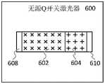
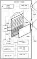
根据本公开的一方面,公开一种SWIR光学系统,所述SWIR系统包括一无源Q开关激光器(在本文中也被称为“P-QS激光器”),所述无源Q开关激光器包括:一增益介质,包括一增益介质结晶(GMC)材料,所述增益介质结晶材料是陶瓷掺钕的钇铝石榴石(Nd:YAG);一可饱和吸收体(SA),被刚性连接到所述增益介质,所述SA包括一陶瓷SA结晶材料,所述陶瓷SA结晶材料选自于由以下材料组成的多个掺杂陶瓷材料的一群组:V3+:YAG及多种掺二价钴结晶材料;及一光腔,所述增益介质和所述SA位于所述光腔中,所述光腔包括一高反射率镜及一输出耦合器。According to one aspect of the present disclosure, a SWIR optical system is disclosed, the SWIR system comprising a passive Q-switched laser (also referred to herein as a "P-QS laser"), the passive Q-switched laser comprising: a gain medium comprising a gain medium crystalline (GMC) material that is ceramic neodymium-doped yttrium aluminum garnet (Nd:YAG); a saturable absorber (SA) rigidly attached to the The gain medium, the SA includes a ceramic SA crystalline material selected from a group of a plurality of doped ceramic materials consisting of V3+ : YAG and a plurality of divalent cobalt doped materials crystalline material; and an optical cavity in which the gain medium and the SA are located, the optical cavity including a high reflectivity mirror and an output coupler.
此后在此说明书中以及为了简单起见,所述术语“可饱和吸收体(saturableabsorber)”经常被替换为缩写“SA”。Hereinafter in this specification and for simplicity, the term "saturable absorber" is often replaced by the abbreviation "SA".
根据本公开的一方面,公开一种SWIR光学系统,所述SWIR系统包括一P-QS激光器,所述P-QS激光器包括:一增益介质,包括一GMC材料,所述GMC材料是陶瓷Nd:YAG;一SA,被刚性连接到所述增益介质,所述SA包括一陶瓷SA结晶材料,所述陶瓷SA结晶材料选自于由以下材料组成的多个掺杂陶瓷材料的一群组:V3+:YAG及多种掺二价钴结晶材料;及一光腔,所述增益介质及所述SA位于所述光腔中,所述光腔包括一高反射率镜及一输出耦合器。According to one aspect of the present disclosure, a SWIR optical system is disclosed, the SWIR system comprising a P-QS laser, the P-QS laser comprising: a gain medium comprising a GMC material, the GMC material being ceramic Nd: YAG; an SA rigidly connected to the gain medium, the SA comprising a ceramic SA crystalline material selected from a group of doped ceramic materials consisting of: V3+ : YAG and various cobalt-doped crystalline materials; and an optical cavity in which the gain medium and the SA are located, the optical cavity including a high reflectivity mirror and an output coupler.
根据本公开的一方面,公开一种SWIR光学系统,其包括一P-QS激光器,所述P-QS激光器包括:一增益介质,所述增益介质包括一陶瓷GMC材料,所述陶瓷GMC材料是陶瓷掺钕稀土元素晶体;一个SA,被刚性连接到所述增益介质,所述SA包括一陶瓷SA结晶材料,所述陶瓷SA结晶材料选自于由以下材料组成的多个掺杂结晶材料组成的一群组:V3+:YAG及多种掺钴结晶材料;及一光腔,所述增益介质及所述SA位于所述光腔中,所述光腔包括一高反射率镜及一输出耦合器。According to one aspect of the present disclosure, there is disclosed a SWIR optical system comprising a P-QS laser, the P-QS laser comprising: a gain medium comprising a ceramic GMC material, the ceramic GMC material being a ceramic neodymium doped rare earth element crystal; an SA rigidly attached to the gain medium, the SA comprising a ceramic SA crystalline material selected from a plurality of doped crystalline materials consisting of A group of: V3+ : YAG and various cobalt-doped crystalline materials; and an optical cavity in which the gain medium and the SA are located, the optical cavity including a high reflectivity mirror and a output coupler.
根据本公开的一方面,公开一种用于制造一P-QS激光器的多个部件的方法,所述方法包括:将至少一种第一粉末塞入一第一模具中;在所述第一模具中压实所述至少一种第一粉末以产出一第一生坯;将不同于所述至少一种第一粉末的至少一种第二粉末塞入一第二模具中;在所述第二模具中压实所述至少一种第二粉末,从而产出一第二生坯;加热所述第一生坯以产出一第一结晶材料;加热所述第二生坯以产出一第二结晶材料;将所述第二结晶材料连接到所述第一结晶材料。在这样的一情况下,所述第一结晶材料及所述第二结晶材料中的一种结晶材料是一掺钕结晶材料,并且是用于所述P-QS激光器的一增益介质,并且其中所述第一结晶材料和第二结晶材料中的另一种结晶材料是用于所述P-QS激光器的一SA,并且选自于由以下材料组成的多个结晶材料的一群组:一掺钕结晶材料及一掺杂结晶材料,所述后者选自于由以下材料组成的多个掺杂结晶材料的群组:V3+:YAG及多种掺钴结晶材料。同样,在这样的一情况下,所述增益介质及所述SA中的至少一种是一陶瓷结晶材料(ceramic crystalline material)。According to one aspect of the present disclosure, a method for fabricating components of a P-QS laser is disclosed, the method comprising: inserting at least one first powder into a first mold; compacting the at least one first powder in a mold to produce a first green body; inserting at least one second powder different from the at least one first powder into a second mold; The at least one second powder is compacted in a second mold to produce a second green body; the first green body is heated to produce a first crystalline material; the second green body is heated to produce a second crystalline material; connecting the second crystalline material to the first crystalline material. In such a case, one crystalline material of the first crystalline material and the second crystalline material is a neodymium-doped crystalline material and is a gain medium for the P-QS laser, and wherein The other crystalline material of the first crystalline material and the second crystalline material is an SA for the P-QS laser, and is selected from a group of crystalline materials consisting of: a A neodymium-doped crystalline material and a doped crystalline material selected from the group of doped crystalline materials consisting of V3+ :YAG and a plurality of cobalt-doped crystalline materials. Also, in such a case, at least one of the gain medium and the SA is a ceramic crystalline material.
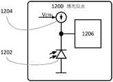
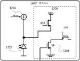
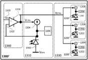
根据本公开的一方面,公开一种PDD,包括:一有源PS,包括一有源PD;一参考PS,包括一参考PD;一第一电压控制电流电路,由一电压控制电流源(voltage-controlledcurrent source)或一电压控制电流汇(voltage-controlled current sink)组成,所述第一电压控制电流电路被连接到所述有源PD;及一控制电压生成电路,被连接到所述有源电压控制电流电路及所述参考PS,并被用于将一控制电压提供给所述电压控制电流电路,所述控制电压具有一电压电平,所述电压电平响应于所述参考PD的暗电流,以减少所述有源PD的暗电流对所述有源PS的一输出的一影响。According to an aspect of the present disclosure, a PDD is disclosed, comprising: an active PS including an active PD; a reference PS including a reference PD; a first voltage-controlled current circuit, which is controlled by a voltage -controlled current source) or a voltage-controlled current sink, the first voltage-controlled current circuit is connected to the active PD; and a control voltage generating circuit is connected to the active PD A voltage-controlled current circuit and the reference PS are used to provide a control voltage to the voltage-controlled current circuit, the control voltage having a voltage level responsive to the darkening of the reference PD current to reduce an influence of the dark current of the active PD on an output of the active PS.
根据本公开的一方面,公开一种减少在一PDD中的暗电流的多个影响的方法,所述方法包括:当所述PDD在一第一温度操作时,基于所述PDD的至少一个参考PD的暗电流决定一第一控制电压;将所述第一控制电压提供给被连接到所述PDD的一有源PS的至少一个有源PD的一第一电压控制电流电路,从而致使所述第一电压控制电流电路在所述有源PS中施加一第一暗电流抵制电流;由所述有源PD生成一第一检测电流,以响应于冲击源于所述PDD的一视场中的一物体的所述有源PD的光以及由所述有源PD生成的暗电流;及由所述有源PS输出一第一检测信号,所述第一检测信号的幅度小于所述第一检测电流,以响应于所述第一检测电流及所述第一暗电流抵制电流,从而补偿暗电流对所述第一检测信号的影响;及当所述PDD在高于所述第一温度至少摄氏10度(℃)的一第二温度操作时,基于所述PDD的至少一个参考PD的暗电流决定一第二控制电压;将所述第二控制电压提供给所述第一电压控制电流电路,从而致使所述第一电压控制电流电路在所述有源PS中施加一第二暗电流抵制电流;由所述有源PD生成一第二检测电流,以响应于冲击源于所述物体的所述有源PD的光以及由所述有源PD生成的暗电流;及由所述有源PS输出一第二检测信号,所述第二检测信号的幅度小于所述第二检测电流,以响应于所述第二检测电流及所述第二暗电流抵制电流,从而补偿暗电流对所述第二检测信号的影响。在这样的一情况下,所述第二暗电流抵制电流的一幅度比所述第一暗电流抵制电流的一幅度更大至少两倍的一因数(a factor ofat least two)。According to an aspect of the present disclosure, a method of reducing the effects of dark current in a PDD is disclosed, the method comprising: when the PDD is operating at a first temperature, based on at least one reference of the PDD The dark current of the PD determines a first control voltage; providing the first control voltage to a first voltage-controlled current circuit of at least one active PD connected to an active PS of the PDD, thereby causing the A first voltage-controlled current circuit applies a first dark current rejection current in the active PS; a first detection current is generated by the active PD in response to impulses originating in a field of view of the PDD; The light of the active PD of an object and the dark current generated by the active PD; and the active PS outputs a first detection signal, the amplitude of the first detection signal is smaller than that of the first detection current to counteract the current in response to the first detection current and the first dark current, thereby compensating for the influence of the dark current on the first detection signal; and when the PDD is at least Celsius above the first temperature When operating at a second temperature of 10 degrees (°C), a second control voltage is determined based on the dark current of at least one reference PD of the PDD; the second control voltage is provided to the first voltage-controlled current circuit, thereby causing the first voltage-controlled current circuit to apply a second dark current resisting current in the active PS; a second detection current is generated by the active PD in response to shocks originating from the object. the light of the active PD and the dark current generated by the active PD; and outputting a second detection signal by the active PS, the amplitude of the second detection signal is smaller than the second detection current, in response to The second detection current and the second dark current are resisted against current, so as to compensate the influence of the dark current on the second detection signal. In such a case, a magnitude of the second dark current rejection current is greater than a magnitude of the first dark current rejection current by a factor of at least two.
根据本公开的一方面,公开一种用于测试一PDD的方法,所述方法包括:将一第一电压提供给一控制电压生成电路的一放大器的一第一输入,其中所述放大器的一第二输入被耦合到一参考PD及一第二电流电路,所述第二电流电路供应处于一水平的电流,所述电流被支配以响应于所述放大器的一输出电压,从而致使所述放大器生成用于所述PDD的一PS的一第一电流电路的一第一控制电压;读取所述PS的一第一输出信号,所述第一输出信号由所述PS生成,以响应于由所述第一电流电路所生成的电流及所述PS的一PD;将不同于所述第一电压的一第二电压提供给所述放大器的所述第一输入,从而致使所述放大器生成用于一第一电流电路的一第二控制电压;读取所述PS的一第二输出信号,所述第二输出信号由所述PS生成,以响应于由所述第一电流电路所生成的电流及所述PS的一PD;及基于所述第一输出信号及所述第二输出信号,决定所述PDD的一检测路径的一缺陷状态,所述检测路径包括所述PS及与所述PS相关联的读出电路。According to an aspect of the present disclosure, a method for testing a PDD is disclosed, the method comprising: providing a first voltage to a first input of an amplifier of a control voltage generation circuit, wherein a The second input is coupled to a reference PD and a second current circuit that supplies current at a level that is dominated in response to an output voltage of the amplifier causing the amplifier generating a first control voltage for a first current circuit of a PS of the PDD; reading a first output signal of the PS, the first output signal being generated by the PS in response to The current generated by the first current circuit and a PD of the PS; a second voltage different from the first voltage is provided to the first input of the amplifier, thereby causing the amplifier to generate a a second control voltage at a first current circuit; reading a second output signal of the PS, the second output signal being generated by the PS in response to a voltage generated by the first current circuit current and a PD of the PS; and determining a defect state of a detection path of the PDD based on the first output signal and the second output signal, the detection path including the PS and the PS associated readout circuitry.
根据本公开的一方面,公开一种用于生成多个图像的系统,所述系统包括:一处理器,所述处理器被配置为:从一PDA接收一物体的多个检测结果,所述物体包括在所有侧面上被多个低反射率表面环绕的一高反射率表面,所述多个检测结果包括在一第一帧曝光时间期间由所述PDA所检测的所述物体的第一帧信息,以及在一第二帧曝光时间期间由所述PDA所检测的所述物体的第二帧信息,所述第二帧曝光时间比所述第一帧曝光时间更长;基于所述第一帧曝光时间处理所述第一帧信息,以提供一第一图像,所述第一图像包括代表所述高反射率表面的一亮区域,所述亮区域被代表所述多个低反射率表面的一暗背景包围;及基于所述第二帧曝光时间处理所述第二帧信息,以提供一第二图像,所述第二图像包括没有一亮区域的一暗背景。According to one aspect of the present disclosure, a system for generating a plurality of images is disclosed, the system comprising: a processor configured to receive a plurality of detection results of an object from a PDA, the The object includes a high reflectivity surface surrounded on all sides by a plurality of low reflectivity surfaces, the plurality of detection results including a first frame of the object detected by the PDA during a first frame exposure time information, and a second frame of information for the object detected by the PDA during a second frame exposure time that is longer than the first frame exposure time; based on the first frame exposure time frame exposure time processing the first frame of information to provide a first image including a bright area representing the high reflectivity surface, the bright area being representative of the plurality of low reflectivity surfaces and processing the second frame information based on the second frame exposure time to provide a second image including a dark background without a bright area.
根据本公开的一方面,公开一种用于生成多个图像的系统,所述系统包括:一处理器,所述处理器被配置为:从一PDA接收一物体的多个检测结果,所述物体包括在所有侧面上被多个低反射率表面环绕的一高反射率表面,所述多个检测结果包括在一第一帧曝光时间期间由所述PDA所检测的所述物体的第一帧信息,以及在一第二帧曝光时间期间由所述PDA所检测的所述物体的第二帧信息,所述第二帧曝光时间比所述第一帧曝光时间更长;基于所述第一帧曝光时间处理所述第一帧信息,以提供一第一图像,所述第一图像包括代表所述高反射率表面的一亮区域,所述亮区域被代表所述多个低反射率表面的一暗背景包围;及基于所述第二帧曝光时间处理所述第二帧信息,以提供一第二图像,所述第二图像包括没有一亮区域的一暗背景。According to one aspect of the present disclosure, a system for generating a plurality of images is disclosed, the system comprising: a processor configured to receive a plurality of detection results of an object from a PDA, the The object includes a high reflectivity surface surrounded on all sides by a plurality of low reflectivity surfaces, the plurality of detection results including a first frame of the object detected by the PDA during a first frame exposure time information, and a second frame of information for the object detected by the PDA during a second frame exposure time that is longer than the first frame exposure time; based on the first frame exposure time frame exposure time processing the first frame of information to provide a first image including a bright area representing the high reflectivity surface, the bright area being representative of the plurality of low reflectivity surfaces and processing the second frame information based on the second frame exposure time to provide a second image including a dark background without a bright area.
根据本公开的一方面,公开一种基于一PDA的数据生成图像信息的方法,所述方法包括:从一PDA接收包括一高反射率区域的一低反射率目标的第一帧信息,所述第一帧信息指示在一第一帧曝光时间期间由所述PDA所检测的所述目标的多个不同部分的多个光强度;基于所述第一帧曝光时间处理所述第一帧信息,以提供一第一图像,所述第一图像包括被一暗背景环绕的一亮区域;从所述PDA接收包括所述高反射率区域的所述低反射率目标的第二帧信息,所述第二帧信息指示在一第二帧曝光时间期间由所述PDA所检测的所述目标的所述多个不同部分的多个光强度,所述第二帧曝光时间长于所述第一帧曝光时间;及基于所述第二帧曝光时间处理所述第二帧信息,以提供一第二图像,所述第二图像包括没有一亮区域的一暗背景。According to an aspect of the present disclosure, a method for generating image information based on data of a PDA is disclosed, the method comprising: receiving from a PDA first frame information of a low reflectivity target including a high reflectivity area, the method comprising: a first frame of information indicating a plurality of light intensities of different parts of the target detected by the PDA during a first frame of exposure time; processing the first frame of information based on the first frame of exposure time, to provide a first image including a bright area surrounded by a dark background; receiving from the PDA a second frame of information for the low reflectivity target including the high reflectivity area, the A second frame of information indicates a plurality of light intensities of the different portions of the target detected by the PDA during a second frame exposure time that is longer than the first frame exposure and processing the second frame information based on the second frame exposure time to provide a second image including a dark background without a bright area.
根据本公开的一方面,公开一种非暂时性计算机可读介质,用于基于一PDA的数据生成图像信息,所述非暂时性计算机可读介质包括被存储在其上的多个指令,所述多个指令在一处理器上被执行时,进行以下步骤:从一PDA接收包括一白色区域的一黑色目标的第一帧信息,所述第一帧信息指示在一第一帧曝光时间期间由所述PDA所检测的所述目标的多个不同部分的多个光强度;基于所述第一帧曝光时间处理所述第一帧信息,以提供一第一图像,所述第一图像包括被一暗背景环绕的一亮区域;从所述PDA接收包括所述白色区域的所述黑色目标的第二帧信息,所述第二帧信息指示在一第二帧曝光时间期间由所述PDA所检测的所述目标的所述多个不同部分的多个指示光强度,所述第二帧曝光时间比所述第一帧曝光时间更长;及基于所述第二帧曝光时间处理所述第二帧信息,以提供一第二图像,所述第二图像包括没有一亮区域的一暗背景。According to one aspect of the present disclosure, a non-transitory computer-readable medium is disclosed for generating image information based on data of a PDA, the non-transitory computer-readable medium including a plurality of instructions stored thereon, the When the plurality of instructions are executed on a processor, the following steps are performed: receiving from a PDA first frame information of a black target including a white area, the first frame information indicating a first frame exposure time period a plurality of light intensities of a plurality of different portions of the target detected by the PDA; processing the first frame of information based on the first frame exposure time to provide a first image, the first image comprising a bright area surrounded by a dark background; receiving from the PDA second frame information of the black target including the white area, the second frame information indicating a second frame of exposure time by the PDA detecting a plurality of indicated light intensities of the plurality of different portions of the target, the second frame exposure time is longer than the first frame exposure time; and processing the second frame exposure time based on the second frame exposure time The second frame of information to provide a second image including a dark background without a bright area.
根据本公开的一方面,公开一种具备动态PS可用性评估的EO系统,所述系统包括:一PDA,包括多个感光位点(PS),每个PS可操作以在多个不同帧输出多个检测信号,由所述相应PS为一帧输出的所述检测信号指示在一相应帧中冲击在所述相应PS上的光量;一可用性过滤模块,可操作以基于一第一帧曝光时间对于每个PS决定所述PS为不可用,并且稍后基于一第二帧曝光时间决定所述PS为可用,所述第二帧曝光时间比所述第一帧曝光时间更短;及一处理器,可操作以基于所述多个PS的多个帧检测水平以生成多个图像。所述处理器,被配置为:(i)在基于多个第一帧检测水平生成一第一图像时,排除由所述可用性过滤模块决定为不可用于所述第一图像的一被滤波的PS的一第一检测信号,以及(ii)当在捕获所述多个第一帧检测水平后基于由所述PDA捕获的多个第二帧检测水平生成一第二图像时,包括由所述可用性过滤模块决定为可用于所述第二图像的所述被滤波的PS的一第二检测信号。According to one aspect of the present disclosure, an EO system with dynamic PS availability assessment is disclosed, the system comprising: a PDA including a plurality of photosensitive sites (PS), each PS operable to output multiple a detection signal output for a frame by the corresponding PS indicating the amount of light impinging on the corresponding PS in a corresponding frame; an availability filter module operable to each PS determines that the PS is unavailable, and later determines the PS to be available based on a second frame exposure time that is shorter than the first frame exposure time; and a processor , operable to detect levels based on a plurality of frames of the plurality of PSs to generate a plurality of images. The processor is configured to: (i) when generating a first image based on a plurality of first frame detection levels, exclude a filtered image determined by the availability filtering module to be unavailable for the first image; a first detection signal of the PS, and (ii) when generating a second image based on the plurality of second frame detection levels captured by the PDA after capturing the plurality of first frame detection levels, including The usability filtering module determines a second detection signal of the filtered PS available for the second image.
根据本公开的一方面,公开一种基于一PDA的数据生成图像信息的方法,所述方法包括:接收第一帧信息,所述第一帧信息包括对于所述PDA的多个PS中的每个PS的一第一帧检测水平,所述第一帧检测水平指示在一第一帧曝光时间期间所述各个PS所检测的一光强度;基于所述第一帧曝光时间,从所述PDD的所述多个PS中识别:一第一可用PS群组,包括一第一个PS、一第二个PS及一第三个PS,以及一第一不可用PS群组,包括一第四个PS;不理会(disregarding)所述第一不可用PS群组的多个第一帧检测水平,基于所述第一可用PS群组的所述多个第一帧检测水平生成一第一图像;在接收所述第一帧信息后,决定一第二帧曝光时间,所述第二帧曝光时间比所述第一帧曝光时间更长;接收第二帧信息,所述第二帧信息包括用于所述PDA的所述多个PS中的每个PS的一第二帧检测水平,所述第二帧检测水平指示在一第二帧曝光时间期间由所述各个PS所检测的一光强度;基于所述第二帧曝光时间,从所述PDD的所述多个PS中识别:一第二可用PS群组,包括所述第一个PS,以及一第二不可用PS群组,包括所述第二个PS、所述第三个PS及所述第四个PS;(g)不理会所述第二不可用PS群组的多个第二帧检测水平,基于所述第二可用PS群组的所述多个第二帧检测水平生成一第二图像;在接收所述第二帧信息后,决定一第三帧曝光时间,所述第三帧曝光时间比所述第一帧曝光时间更长且比所述第二帧曝光时间更短;接收第三帧信息,所述第三帧信息包括对于所述PDA的所述多个PS中的每个PS的一第三帧检测水平,所述第三帧检测水平指示在一第三帧曝光时间期间由所述各个PS所检测的一光强度;基于所述第三帧曝光时间,从所述PDD的所述多个PS中识别:一第三可用PS群组,包括所述第一个PS及所述第二个PS,以及一第三不可用PS群组,包括所述第三个PS及所述第四个PS;及(k)不理会所述第三不可用PS群组的多个第三帧检测水平,基于所述第三可用PS群组的所述多个第三帧检测水平生成一第三图像。According to an aspect of the present disclosure, a method for generating image information based on data of a PDA is disclosed, the method comprising: receiving first frame information, where the first frame information includes information for each of a plurality of PSs of the PDA. a first frame detection level of each PS, the first frame detection level indicating a light intensity detected by the respective PS during a first frame exposure time; based on the first frame exposure time, from the PDD Identify among the plurality of PSs: a first available PS group, including a first PS, a second PS, and a third PS, and a first unavailable PS group, including a fourth PS PS; disregarding the multiple first frame detection levels of the first unavailable PS group, and generating a first image based on the multiple first frame detection levels of the first available PS group ; After receiving the first frame information, determine a second frame exposure time, the second frame exposure time is longer than the first frame exposure time; Receive second frame information, the second frame information includes A second frame detection level for each PS in the plurality of PSs of the PDA, the second frame detection level indicating a light detected by the respective PS during a second frame exposure time Intensity; based on the second frame exposure time, identifying from the plurality of PSs of the PDD: a second available PS group, including the first PS, and a second unavailable PS group, including the second PS, the third PS, and the fourth PS; (g) disregarding multiple second frame detection levels of the second unavailable PS group, based on the second PS A second image can be generated by using the plurality of second frame detection levels of the PS group; after receiving the second frame information, a third frame exposure time is determined, and the third frame exposure time is longer than the first frame exposure time. the frame exposure time is longer and shorter than the second frame exposure time; receiving third frame information, the third frame information including a third frame for each PS of the plurality of PSs of the PDA detection level, the third frame detection level indicating a light intensity detected by the respective PSs during a third frame exposure time; based on the third frame exposure time, from the plurality of PSs of the PDD Middle identification: a third available PS group, including the first PS and the second PS, and a third unavailable PS group, including the third PS and the fourth PS and (k) disregarding the plurality of third frame detection levels of the third unavailable PS group, generating a third image based on the plurality of third frame detection levels of the third available PS group.
根据本公开的一方面,公开一种非暂时性计算机可读介质,用于基于一光电检测器阵列(PDA)的数据生成图像信息,所述非暂时性计算机可读介质包括被存储在其上的多个指令,所述多个指令在一处理器上被执行时,进行以下步骤:接收第一帧信息,所述第一帧信息包括对于所述PDA的多个PS中的每个PS的一第一帧检测水平,所述第一帧检测水平指示在一第一帧曝光时间期间由所述各个PS所检测的一光强度;基于所述第一帧曝光时间,从所述PDD的所述多个PS中识别:一第一可用PS群组,包括一第一个PS、一第二个PS及一第三个PS,以及一第一不可用PS群组,包括一第四个PS;不理会所述第一不可用PS群组的多个第一帧检测水平,基于所述第一可用PS群组的所述第一帧检测水平生成一第一图像;在接收所述第一帧信息后,决定一第二帧曝光时间,所述第二帧曝光时间比所述第一帧曝光时间更长;接收第二帧信息,所述第二帧信息包括用于所述PDA的所述多个PS中的每个PS的一第二帧检测水平,所述第二帧检测水平指示在一第二帧曝光时间期间由所述各个PS所检测的一光强度;基于第二帧曝光时间,从所述PDD的所述多个PS中识别:一第二可用PS群组,包括所述第一个PS,以及一第二不可用PS群组,包括所述第二个PS、所述第三个PS及所述第四个PS;不理会所述第二不可用PS群组的多个第二帧检测水平,基于所述第二可用PS群组的所述多个第二帧检测水平生成一第二图像;在接收所述第二帧信息后,决定一第三帧曝光时间,所述第三帧曝光时间比所述第一帧曝光时间更长且比所述第二帧曝光时间更短;接收第三帧信息,所述第三帧信息包括用于所述PDA的所述多个PS中的每个PS的一第三帧检测水平,所述第三帧检测水平指示在一第三帧曝光时间期间由所述各个PS所检测的一光强度;基于所述第三帧曝光时间,从所述PDD的多个PS中识别:一第三可用PS群组,包括所述第一个PS及所述第二个PS,以及一第三不可用PS群组,包括所述第三个PS及所述第四个PS;及不理会所述第三不可用PS群组的多个第三帧检测水平,基于所述第三可用PS群组的所述多个第三帧检测水平生成一第三图像。According to one aspect of the present disclosure, a non-transitory computer-readable medium is disclosed for generating image information based on data of a photodetector array (PDA), the non-transitory computer-readable medium comprising stored thereon multiple instructions, when the multiple instructions are executed on a processor, the following steps are performed: receiving first frame information, the first frame information includes information for each PS in the multiple PSs of the PDA a first frame detection level indicating a light intensity detected by the respective PSs during a first frame exposure time; based on the first frame exposure time, from all of the PDD's Identify among the plurality of PSs: a first available PS group, including a first PS, a second PS, and a third PS, and a first unavailable PS group, including a fourth PS ; Ignore the multiple first frame detection levels of the first unavailable PS group, and generate a first image based on the first frame detection levels of the first available PS group; After the frame information, a second frame exposure time is determined, and the second frame exposure time is longer than the first frame exposure time; the second frame information is received, and the second frame information includes all the information used for the PDA. a second frame detection level of each PS in the plurality of PSs, the second frame detection level indicating a light intensity detected by the respective PS during a second frame exposure time; based on the second frame exposure time, identified from the plurality of PSs of the PDD: a second available PS group, including the first PS, and a second unavailable PS group, including the second PS, all the third PS and the fourth PS; regardless of the multiple second frame detection levels of the second unavailable PS group, based on the multiple second frames of the second available PS group The detection level generates a second image; after receiving the second frame information, a third frame exposure time is determined, and the third frame exposure time is longer than the first frame exposure time and longer than the second frame exposure time shorter exposure time; receiving third frame information including a third frame detection level for each PS in the plurality of PSs of the PDA, the third frame detection level indicating a light intensity detected by the respective PSs during a third frame exposure time; based on the third frame exposure time, identifying from the plurality of PSs of the PDD: a third available PS group including all the first PS and the second PS, and a third unavailable PS group including the third PS and the fourth PS; and disregarding the third unavailable PS group and generating a third image based on the plurality of third frame detection levels of the third available PS group.
附图简要说明Brief Description of Drawings
下面参考在此段落后被列出的附图以描述本文公开的实施例的非限制性示例。在一个以上的图中出现的相同结构、元件或部件可以在它们出现的所有图中用相同的数字被标记。所述附图及描述意在说明及阐明本文公开的实施例,并且不应被认为以任何方式进行限制。所有附图示出根据当前公开的主题的诸多示例的装置或流程图。在附图中:Non-limiting examples of the embodiments disclosed herein are described below with reference to the figures listed after this paragraph. The same structures, elements or components that appear in more than one figure may be labeled with the same numerals in all the figures in which they appear. The drawings and description are intended to illustrate and clarify the embodiments disclosed herein, and should not be considered limiting in any way. All of the figures illustrate apparatus or flow diagrams according to various examples of the presently disclosed subject matter. In the attached image:
图1A、图1B及图1C是以图解说明多个有源SWIR成像系统的多个示意性框图。1A, 1B, and 1C are various schematic block diagrams illustrating various active SWIR imaging systems.
图2是以图解说明在一SWIR成像系统中在多个积分时间的不同持续时间后的噪声功率的相对幅度的一示例性图形;2 is an exemplary graph illustrating the relative magnitude of noise power after different durations of multiple integration times in a SWIR imaging system;
图3A、图3B及图3C分别示出根据一些实施例的一有源SWIR成像系统的一操作方法的一流程图及多个示意图;3A, 3B, and 3C respectively illustrate a flowchart and schematic diagrams of a method of operation of an active SWIR imaging system according to some embodiments;
图4A、图4B及图4C分别示出一有源SWIR成像系统的一示例性操作方法的一流程图及多个示意图;4A, 4B, and 4C respectively illustrate a flowchart and schematic diagrams of an exemplary method of operation of an active SWIR imaging system;
图5是以图解说明用于一种在一EO系统的一FOV中生成多个物体的多个SWIR图像的方法的一流程图;5 is a flowchart illustrating a method for generating SWIR images of objects in a FOV of an EO system;
图6是示出一SWIR光学系统的一示例的一示意性功能框图。FIG. 6 is a schematic functional block diagram illustrating an example of a SWIR optical system.
图7A、图7B及图7C是以图解说明P-QS激光器的多个示例的多个示意性功能框图。7A, 7B, and 7C are various schematic functional block diagrams illustrating various examples of P-QS lasers.
图8及图9是以图解说明一SWIR光学系统的多个示意性功能图。8 and 9 are schematic functional diagrams illustrating a SWIR optical system.
图10是以图解说明一SWIR光学系统的一示例的一示意性功能框图。10 is a schematic functional block diagram illustrating an example of a SWIR optical system.
图11A、图11B及图11C分别示出以图解说明一种用于制造一P-QS激光器的多个部件的方法的一示例的一流程图以及用于执行所述方法的多个概念性时间轴。11A, 11B, and 11C respectively show a flowchart to illustrate an example of a method for fabricating components of a P-QS laser and conceptual times for performing the method axis.
图12A示意性地示出一PS包括一PD,所述PD由一电压控制电流源控制;FIG. 12A schematically shows that a PS includes a PD controlled by a voltage-controlled current source;
图12B示意性地示出一PS包括一PD,所述PD以一“3T”结构由一电压控制电流源控制;Figure 12B schematically shows a PS including a PD controlled by a voltage-controlled current source in a "3T" configuration;
图13A及图13B示出一PDD,所述PDD包括一PS及可操作以降低暗电流影响的电路。13A and 13B illustrate a PDD that includes a PS and circuitry operable to reduce the effects of dark current.
图13C示出一PDD,所述PDD包括多个PS及可操作以降低暗电流影响的电路;13C shows a PDD including a plurality of PSs and circuitry operable to reduce the effects of dark current;
图14示出PDD的示例性PD IV曲线及可能的工作电压;Figure 14 shows exemplary PD IV curves and possible operating voltages for PDDs;
图15示出一控制电压生成电路,所述控制电压生成电路被连接到多个参考感光位点;Figure 15 shows a control voltage generation circuit connected to a plurality of reference photosensitive sites;
图16A及图16B示出多个PDD,所述多个PDD包括多个PS的一阵列及基于多个PD的参考电路;Figures 16A and 16B illustrate a plurality of PDDs comprising an array of PSs and reference circuits based on the plurality of PDs;
图17及图18示出多个PDD,每个PDD包括一PS及可操作用于降低暗电流影响的电路;17 and 18 illustrate a plurality of PDDs, each PDD including a PS and circuitry operable to reduce the effects of dark current;
图19以图解说明一PDD,所述PDD包括光学器件、一处理器及多个附加构件;19 illustrates a PDD including optics, a processor, and additional components;
图20是以图解说明一种用于补偿在一光电检测器中的暗电流的方法的一流程图;20 is a flowchart illustrating a method for compensating for dark current in a photodetector;
图21是以图解说明一种用于补偿在一光电检测器中的暗电流的方法的一流程图;21 is a flowchart illustrating a method for compensating for dark current in a photodetector;
图22是以图解说明一种用于测试一光电检测器的方法的一流程图;22 is a flow chart illustrating a method for testing a photodetector;
图23以图解说明根据一些实施例的一EO系统;Figure 23 illustrates an EO system according to some embodiments;
图24以图解说明一种基于一PDA的数据生成图像信息的方法的一示例;24 illustrates an example of a method of generating image information based on data from a PDA;
图25及图26分别示出以图解说明一种用以在不同帧曝光时间对于PDA操作生成一模型的方法的一流程图及所述方法对于在不同帧曝光时间拍摄相同场景的不同帧执行所述方法的一图形表征;Figures 25 and 26 show a flow chart, respectively, to illustrate a method for generating a model for PDA operation at different frame exposure times and the method performs all steps for different frames of the same scene captured at different frame exposure times. a graphical representation of the method;
图27是以图解说明一种用以在不同操作条件基于多个PS的不同子集生成多个图像的方法的一示例的一流程图;27 is a flowchart illustrating an example of a method to generate multiple images based on different subsets of multiple PSs at different operating conditions;
图28A及28B以图解说明一EO系统及多个示例性目标物体;28A and 28B illustrate an EO system and exemplary target objects;
图29是以图解说明一种基于一PDA的数据生成图像信息的方法的一流程图。29 is a flow chart illustrating a method of generating image information based on data from a PDA.
将被理解的是,为了图例的简化及清楚起见,在附图中被示出的诸多元件未必按比例绘制。例如:为了清楚起见,一些元件的尺寸可能相对于其它元件被放大。此外,在被认为适当的情况下,诸多附图标记可以在诸多附图之间被重复以指示诸多对应或相似的元件。It will be appreciated that for simplicity and clarity of illustration, various elements shown in the figures have not necessarily been drawn to scale. For example, the dimensions of some elements may be exaggerated relative to other elements for clarity. Further, where considered appropriate, reference numerals may be repeated among the figures to indicate corresponding or analogous elements.
具体实施方式Detailed ways
在以下详细描述中,阐述许多具体细节以提供本公开的透彻理解。然而,本领域技术人员将理解的是,本公开可以在没有这些具体细节的情况下被实践。在其它情况下,公知方法、过程及构件未被详细描述,以免混淆本公开。In the following detailed description, numerous specific details are set forth in order to provide a thorough understanding of the present disclosure. However, it will be understood by those skilled in the art that the present disclosure may be practiced without these specific details. In other instances, well-known methods, procedures, and components have not been described in detail so as not to obscure the present disclosure.
在阐述的附图及描述中,相同的附图标记指示不同实施例或配置共有的那些构件。In the figures and descriptions set forth, like reference numerals refer to those components that are common to different embodiments or configurations.
除非另有特别说明,否则从以下讨论中可以明显看出,被理解的是,在整个说明书讨论中,使用诸如“处理(processing)”、“计算(calculating)”、“计算(computing)”、“决定(determining)”、“生成(generating)”、“设置(setting)”、“配置(configuring)”等术语、”选择(selecting)”、“定义(defining)”等包括将数据操纵及/或变换为其它数据的一计算机的动作及/或过程,所述数据被表示为物理量,譬如诸多电子量,及/或表示所述诸多物理物体的数据。Unless specifically stated otherwise, it will be apparent from the following discussion that it is understood that throughout the discussion of the specification, uses such as "processing", "calculating", "computing", Terms such as "determining", "generating", "setting", "configuring", "selecting", "defining", etc. include manipulating data and/or Or the action and/or process of a computer that is transformed into other data represented as physical quantities, such as electronic quantities, and/or data representing the physical objects.
所述术语“计算机(computer)”、“处理器(processor)”及“控制器(controller)”应被广义地解释为涵盖具备数据处理能力的任何种类的电子装置,通过非限制的示例包括:一个人计算机、一服务器、一计算系统、一通信装置、一处理器(譬如数字信号处理器(DSP)、一微控制器、一现场可编程门阵列(FPGA)、一专用集成电路等)、任何其它电子计算装置,或其任意组合。The terms "computer", "processor" and "controller" should be construed broadly to encompass any kind of electronic device capable of data processing including, by way of non-limiting example: a personal computer, a server, a computing system, a communication device, a processor (such as a digital signal processor (DSP), a microcontroller, a field programmable gate array (FPGA), an application specific integrated circuit, etc.), Any other electronic computing device, or any combination thereof.
根据本文的教导的操作可以由为了期望目的而被特别建构的一计算机或由为了期望目的而被特别配置的一通用计算机通过被存储在一计算机可读存储介质中的一计算机程序被执行。Operations in accordance with the teachings herein may be performed by a computer program stored in a computer-readable storage medium by a computer specially constructed for the desired purposes or by a general purpose computer specially configured for the desired purposes.
如本文中所使用的,所述短语“例如(for example)”、“诸如(such as)”、“比如(for instance)”及其词型变化描述当前公开的主题的诸多非限制性实施例。在说明书中对“一种情况(one case)”、“一些情况(some cases)”、“其它情况(other cases)”或其词型变化的引用意谓着结合实施例被描述的一特定特征、结构或特性被包括在当前公开的主题的至少一个实施例中。因此,所述短语“一种情况(one case)”、“一些情况(some cases)”、“其它情况(other cases)”或其词型变化的出现不一定意指相同的(多个)实施例。As used herein, the phrases "for example," "such as," "for instance," and inflections thereof describe many non-limiting embodiments of the presently disclosed subject matter . References in the specification to "one case", "some cases", "other cases" or conjugations thereof mean that a particular feature is described in connection with the embodiment , structure or characteristic are included in at least one embodiment of the presently disclosed subject matter. Thus, appearances of the phrases "one case," "some cases," "other cases," or inflections thereof do not necessarily mean the same implementation(s) example.
应当理解的是,为了清楚起见,在诸多单独的实施例的上下文中被描述的当前公开的主题的某些特征也可以在单个实施例中以组合被提供。相反地,为了简洁起见,在单个实施例的上下文中被描述的当前公开的主题的各种特征也可以单独地或以任何合适的子组合被提供。It should be appreciated that certain features of the presently disclosed subject matter that are, for clarity, described in the context of separate embodiments, may also be provided in combination in a single embodiment. Conversely, various features of the presently disclosed subject matter that are, for brevity, described in the context of a single embodiment, may also be provided separately or in any suitable subcombination.
在当前公开的主题的诸多实施例中,在附图中被以图解说明的一个或多个阶段或步骤可以用不同顺序被执行及/或一个或多个阶段群组可以同时被执行,反之亦然。所述诸多附图以图解说明根据当前公开的主题的一实施例的系统架构的一总体示意图。在诸多附图中的每个模块可以由进行本文所定义及解释的诸多功能的软件、硬件及/或固件的任何组合组成。在诸多附图中的所述诸多模块可以被集中在一个位置或被分散在一个以上的位置。In various embodiments of the presently disclosed subject matter, one or more phases or steps illustrated in the figures may be performed in a different order and/or one or more groups of phases may be performed concurrently, and vice versa Of course. The figures are used to illustrate a general schematic view of the system architecture according to an embodiment of the presently disclosed subject matter. Each module in the figures may be comprised of any combination of software, hardware and/or firmware that performs the functions defined and explained herein. The modules in the figures may be grouped in one location or dispersed in more than one location.
在说明书中对一方法的任何引用应被比照(mutatis mutandis)应用于能够执行所述方法的一系统,并且应该比照应用于存储诸多指令的一非暂时性计算机可读介质,所述指令一旦由一计算机执行,引起执行所述方法。Any reference in the specification to a method shall mutatis mutandis apply to a system capable of performing the method, and shall apply mutatis mutandis to a non-transitory computer readable medium storing instructions once created by A computer execution causes the method to be performed.
在说明书中对一系统的任何引用应被比照应用于能够由所述系统执行的一方法,并且应该比照应用于存储诸多指令的一非暂时性计算机可读介质,所述指令可由所述系统执行。Any reference in the specification to a system shall apply mutatis mutandis to a method capable of being performed by the system, and shall apply mutatis mutandis to a non-transitory computer readable medium storing instructions executable by the system .
在说明书中对一非暂时性计算机可读介质或类似术语的任何引用应被比照应用于能够执行被存储在所述非暂时性计算机可读介质中的所述诸多指令,并且应被比照应用于可由一计算机执行的方法,所述计算机读取被存储在所述非暂时性计算机可读介质中的所述诸多指令。Any reference in the specification to a non-transitory computer-readable medium or similar terms shall apply mutatis mutandis to the instructions capable of executing the instructions stored in the non-transitory computer-readable medium, and shall apply mutatis mutandis A method executable by a computer that reads the instructions stored in the non-transitory computer readable medium.
除非另有定义,否则本文中使用的所有技术及科学术语具有与本公开所属领域的普通技术人员通常所理解的相同含义。本文提供的材料、方法及示例仅是说明性的,并非意图被限制。Unless otherwise defined, all technical and scientific terms used herein have the same meaning as commonly understood by one of ordinary skill in the art to which this disclosure belongs. The materials, methods, and examples provided herein are illustrative only and not intended to be limiting.
本公开的方法及系统的实现涉及手动、自动或其一组合以进行或完成某些被选择的任务或步骤。而且,根据本公开的方法及系统的优选实施例的实际仪器及设备,可以通过硬件或通过在任何固件的任何操作系统上的软件或其一组合以实现几个被选择的步骤。例如:作为硬件,本公开的多个被选择的步骤可以被实现为一芯片或一电路。作为软件,本公开的多个被选择的步骤可以被实现为由一计算机使用任何合适的操作系统以执行的多个软件指令。在任何情况下,本公开的方法及系统的多个被选择的步骤可以被描述为由一数据处理器进行,诸如用于执行多个指令的一计算平台。Implementations of the methods and systems of the present disclosure involve manual, automatic, or a combination thereof to perform or complete certain selected tasks or steps. Furthermore, several selected steps may be implemented by hardware or by software on any operating system of any firmware, or a combination thereof, according to actual instrumentation and equipment of preferred embodiments of the method and system of the present disclosure. For example, as hardware, selected steps of the present disclosure may be implemented as a chip or a circuit. As software, selected steps of the present disclosure may be implemented as software instructions to be executed by a computer using any suitable operating system. In any event, selected steps of the methods and systems of the present disclosure may be described as being performed by a data processor, such as a computing platform for executing a plurality of instructions.
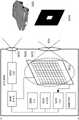
图1A、图1B及图1C是分别以图解说明根据当前公开的主题的多个示例的多个有源SWIR成像系统100、100’及100”的多个示意性框图。1A, 1B, and 1C are various schematic block diagrams, respectively, to illustrate a number of active
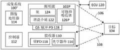
如本文中被使用的,一“有源(active)”成像系统可操作以检测从它的视场(FOV)到达所述系统的光,由包括多个PD的一成像接收器对它进行检测,并且处理所述多个检测信号以提供所述视场或其一部分的一个或多个图像。所述术语“图像(image)”意指由所述成像系统检测的一场景的数字表征,所述成像系统存储在所述图像中的每个元件(像素)的一颜色值,每个像素颜色代表从所述视场(譬如所述FOV的一0.02°乘0.02°的部分,具体取决于接收器光学器件)的不同部位到达所述成像系统的光。要被注意的是,可选地,所述成像系统还可被操作以生成在所述FOV中的诸多物体或光的其它表征(譬如一深度图、3D模型、多边形网格),但是所述术语“图像”意指没有深度数据的二维(2D)图像。As used herein, an "active" imaging system is operable to detect light reaching the system from its field of view (FOV), which is detected by an imaging receiver comprising a plurality of PDs , and processing the plurality of detection signals to provide one or more images of the field of view or a portion thereof. The term "image" means a digital representation of a scene detected by the imaging system that stores a color value for each element (pixel) in the image, each pixel color Represents light reaching the imaging system from different parts of the field of view (eg, a 0.02° by 0.02° portion of the FOV, depending on receiver optics). It is to be noted that, optionally, the imaging system may also be operable to generate other representations of objects or light in the FOV (eg a depth map, 3D model, polygon mesh), but the The term "image" means a two-dimensional (2D) image without depth data.
系统100包括一照明源(IS)102,所述照明源(IS)可操作以朝向一个或多个目标104发射在SWIR波段中的多个辐射脉冲,引起来自所述物体的被反射辐射在系统100的方向上被反射回去。在图1A中,出射照明(outgoing illumination)被标示为106,并且朝向系统100被反射的照明被标示为108。所述被发射的辐射的诸多部分也可能在其它方向上被反射、被偏转或被所述目标吸收。所述术语“目标(target)”意指所述成像传感器的所述FOV中的任何物体(object),诸如固体、液体、柔性及刚性物体。这样的物体的一些非限制性示例包括车辆、道路、人、动物、植物、建筑物、电子设备、云、微观样品、制造中的物品等。可以使用任何合适类型的照明源102,例如一个或多个激光器、一个或多个发光二极管(LED)、一个或多个冲击闪光灯、以上的任意组合等。如下面更详细地讨论的,照明源102可以可选地包括一个或多个有源激光器,或一个或多个P-QS激光器。The
系统100还包括至少一个成像接收器(或简称为“接收器(receiver)”)110,所述成像接收器110包括可操作用于检测所述被反射的SWIR辐射的多个锗(Ge)PD。接收器为多个锗PD中的每个生成一电信号,所述电信号表示在它的可检测光谱范围内冲击SWIR光量。所述量包括从目标反射的SWIR辐射脉冲光量,并且还可以包括:附加的SWIR光(譬如从太阳或从外部光源抵达)。
所述术语“锗PD(Ge PD)”涉及其中在所述锗内、在一锗合金内(譬如SiGe)内或在锗(或锗合金)与另一种材料(譬如硅,SiGe)之间的界面上发生光诱导的电子激发(后来可检测为光电流)的任何PD。具体地,所述术语“锗PD”既涉及纯锗PD,也适用于锗-硅PD。当包含锗及硅的锗PD被使用时,可以使用不同浓度的天竺葵。例如:锗PD中的锗的相对部分(无论是以硅合金化还是与其相邻)可以是在5%与99%的范围内。例如:在多个锗PD中锗的相对部分可以是在15%与40%之间。要被注意的是,除了硅之外的材料也可以是锗PD的一部分,例如铝、镍、硅化物或任何其它合适的材料。在本公开的一些实现方案中,所述多个锗PD可以是纯锗PD(包括大于99.0%的锗)。The term "germanium PD (Ge PD)" relates to where within the germanium, within a germanium alloy (eg SiGe) or between germanium (or germanium alloy) and another material (eg silicon, SiGe) Any PD in which photoinduced electronic excitation (later detectable as photocurrent) occurs at the interface. Specifically, the term "germanium PD" refers to both pure germanium PDs and germanium-silicon PDs. Different concentrations of geranium can be used when germanium PDs containing germanium and silicon are used. For example: the relative fraction of germanium in a germanium PD (whether alloyed with or adjacent to silicon) may be in the range of 5% and 99%. For example: the relative fraction of germanium in a plurality of germanium PDs may be between 15% and 40%. It is noted that materials other than silicon can also be part of the germanium PD, such as aluminum, nickel, suicide, or any other suitable material. In some implementations of the present disclosure, the plurality of germanium PDs may be pure germanium PDs (including greater than 99.0% germanium).
要被注意的是,所述接收器可以被实现为在单个芯片上被制造的一PDA。遍及本公开被讨论的任何所述PD阵列都可以被用作接收器110。所述锗PD可以用任何合适的布置被布置,诸如一矩形矩阵(锗PD的直行及直列)、蜂窝平铺(honeycomb tiling),及甚至是不规则构造。优选地,在所述接收器中的锗PD的数量允许生成高分辨率图像。例如:诸多PD的数量可以在1兆像素、10兆像素或更多的规模的数量级上。It is noted that the receiver can be implemented as a PDA fabricated on a single chip. Any of the PD arrays discussed throughout this disclosure may be used as receiver 110 . The germanium PDs can be arranged in any suitable arrangement, such as a rectangular matrix (straight rows and columns of germanium PDs), honeycomb tiling, and even irregular configurations. Preferably, the number of germanium PDs in the receiver allows high resolution images to be generated. For example, the number of PDs may be on the order of 1 megapixel, 10 megapixel or more.
在一些实施例中,接收器110具有以下规格:In some embodiments, the receiver 110 has the following specifications:
a.HFOV(水平视场)[m]:60a.HFOV (horizontal field of view) [m]: 60
b.WD(工作距离)[m]:150b.WD (working distance) [m]: 150
c.像素尺寸[um]:10c. Pixel size [um]: 10
d.分辨率(在目标上)[mm]:58d. Resolution (on target) [mm]: 58
e.像素#[H]:1,050e. Pixel #[H]: 1,050
f.像素#[V]:1112f. Pixel #[V]: 1112
g.长宽比:3:1g. Aspect ratio: 3:1
h.视角[rad]:0.4h. Angle of view [rad]: 0.4
i.目标的反射率[%]:10%i. Target reflectivity [%]: 10%
j.收集(假设目标反射率为100%并假设为朗伯反射率,被收集的光子与被发射的光子的比率):3e-9。j. Collection (ratio of collected photons to emitted photons assuming 100% target reflectivity and assuming Lambertian reflectivity): 3e-9 .
除了如上所述的冲击SWIR光以外,所述多个锗PD中的每个生成的所述电信号还代表:In addition to impinging SWIR light as described above, the electrical signal generated by each of the plurality of germanium PDs also represents:
a.读出噪声,是随机的,它的幅度与积分时间无关(或实质上无关)。这种噪声的示例包括奈奎斯特·约翰逊(Nyquist Johnson)噪声(也称为热噪声或kTC噪声)。除了统计分量之外,所述读出过程还可以将一DC分量引入所述信号中,但是所述术语“读出噪声(readout noise)”涉及由所述读出过程所引入的所述信号的所述随机分量。a. Readout noise, which is random and whose magnitude is independent (or substantially independent) of the integration time. Examples of such noise include Nyquist Johnson noise (also known as thermal noise or kTC noise). In addition to the statistical component, the readout process may also introduce a DC component into the signal, but the term "readout noise" refers to the variation of the signal introduced by the readout process the random component.
b.暗电流噪声,是随机的,并且在积分时间内会被累积(即,它取决于积分时间)。除了统计分量之外,暗电流还将一直流分量(其可以被消除或可以不被消除,譬如为如关于图12A至图22被讨论的)引入所述信号,但是所述术语“暗电流噪声(dark current noise)”属于由暗电流在所述积分时间内被累积的所述信号的所述随机分量。b. Dark current noise, which is random and accumulates over the integration time (ie, it depends on the integration time). In addition to statistical components, dark current introduces a DC component (which may or may not be eliminated, such as as discussed with respect to Figures 12A-22) into the signal, but the term "dark current noise" (dark current noise)" belongs to the random component of the signal accumulated over the integration time by the dark current.
一些锗PD,尤其是将锗与另一种材料(譬如诸如硅)结合在一起的某些PD,其特征在于一相对较高水平的暗电流。例如:多个锗PD的所述暗电流可能大于50μA/cm2(与所述PD的一表面积有关),甚至更大(譬如大于100μA/cm2、大于200μA/cm2或大于500μA/cm2)。取决于所述PD的表面积,这样多个水平的暗电流可以被转换为每锗PD为50皮安(pA)或更高(譬如每锗PD超过100pA、每锗PD超过200pA、每锗PD超过500pA,或每锗PD超过2nA)。要被注意的是,可以使用不同尺寸的多个PD,诸如大约10mm2、大约50mm2、大约100mm2、大约500mm2。要被注意的是,当所述多个锗PD经受不同水平的非零偏压(nonzero bias)时,所述多个锗PD可能生成不同幅度的暗电流(这在所述多个锗PD中的每个上引起例如大于50皮安的暗电流)。Some germanium PDs, especially some PDs that combine germanium with another material such as silicon for example, are characterized by a relatively high level of dark current. For example, the dark current of multiple germanium PDs may be greater than 50 μA/cm2 (related to a surface area of the PD), or even greater (eg, greater than 100 μA/cm2 , greater than 200 μA/cm2 , or greater than 500 μA/cm2 ) ). Depending on the surface area of the PD, such multiple levels of dark current can be converted to 50 picoamps (pA) or more per germanium PD (eg, over 100 pA per germanium PD, over 200 pA per germanium PD, over 500pA, or over 2nA per germanium PD). It is to be noted that multiple PDs of different sizes can be used, such as about 10mm2 , about 50mm2 , about 100mm2 , about 500mm2 . It is to be noted that when the germanium PDs are subjected to different levels of nonzero bias, the germanium PDs may generate dark currents of different magnitudes (this is the case in the germanium PDs) induces, for example, a dark current greater than 50 pA on each of the .
系统100还包括一控制器112及图像处理器114,所述控制器112控制接收器110(以及可选地还控制照明源(IS)102及/或其它构件)的操作。因此,控制器112被配置为在一相对短的积分时间内控制接收器110的激活,从而限制暗电流噪声的累积对信号质量的影响。例如:控制器112可以操作为在一积分时间内控制接收器110的激活,在所述积分时间内所述被累积的暗电流噪声不超过所述无关积分时间的读出噪声。
现在参考图2,图2是以图解说明根据本公开的主题的诸多示例的在多个积分时间的不同持续时间后的噪声功率的相对幅度的一示例性图形。对于一给定的激光脉冲能量,信噪比(SNR)主要由噪声水平决定,所述噪声水平包括所述暗电流噪声(所述暗光电流的噪声)及热噪声(也被称为kTC噪声)。如图2的示例性图形所示,取决于基于锗的接收器110的积分时间,所述暗电流噪声或所述热噪声在影响所述PD的所述电信号的所述SNR中占主导地位。由于控制器112在一相对短的时间内(在图2中被指定为“A”的范围内)限制所述锗光电检测器的激活时间,因此,没有太多的来自暗电流噪声的电子被收集,因此SNR被改善并且因此主要受热噪声影响。对于一更长的接收器积分时间,在影响所述接收器的SNR时,源于所述锗光电检测器的所述暗电流的所述噪声将超过所述热噪声,从而引起接收器性能下降。要被注意的是,图2的图形仅是说明性的,并且所述暗电流噪声随时间的累积通常随着时间的平方根而增加
回到系统100,要被注意的是,控制器112可以控制接收机110的激活,以用于更短的积分时间(譬如积分时间,在所述积分时间期间所述被累积的暗电流噪声不超过所述读出噪声的一半或所述读出噪声的四分之一)。要被注意的是,除非特别需要,否则将所述积分时间限制在非常低的水平会限制可以被检测的多个光感应信号的数量,并且会使有关热噪声的SNR变差。要被注意的是,适合于读取多个嘈杂信号的多个读出电路中的热噪声电平(需要收集相对较高的信号电平)会引入不可忽略的读出噪声,这可能会严重降低所述SNR。Returning to the
在一些实现方案中,控制器112可以应用稍长的积分时间(譬如积分时间,在所述积分时间期间所述被累积的暗电流噪声不超过所述读出噪声的两倍或所述读出噪声的×1.5)。In some implementations, the
本文公开的示例性实施例涉及用于使用包括基于锗的多个PD的多个接收机的高SNR有源SWIR成像的多个系统及多个方法。与砷化镓铟技术相比,锗接收器技术的主要优势是与CMOS工艺流程的兼容性,允许将所述接收器作为一CMOS产出线的一部分进行制造。例如:通过在一硅(Si)衬底上生长多个Ge外延层,诸如采用Si光子学,多个锗PD可以被集成到CMOS工艺流程中。因此,诸多锗PD也比等效的诸多砷化镓铟(InGaAs)PD更具成本效益。Exemplary embodiments disclosed herein relate to systems and methods for high SNR active SWIR imaging using multiple receivers including germanium-based PDs. The main advantage of germanium receiver technology over gallium indium arsenide technology is compatibility with CMOS process flows, allowing the receiver to be fabricated as part of a CMOS production line. For example, by growing multiple Ge epitaxial layers on a silicon (Si) substrate, such as using Si photonics, multiple germanium PDs can be integrated into a CMOS process flow. Therefore, many germanium PDs are also more cost-effective than equivalent many indium gallium arsenide (InGaAs) PDs.
为了利用诸多锗PD,在本文被公开的一示例性系统适于克服诸多锗二极管的相对较高的暗电流的限制,通常在约50uA/cm^2的范围内。通过使用具有短捕获时间及诸多高功率激光脉冲的一组合的有源成像,所述暗电流问题可以被克服。To utilize germanium PDs, an exemplary system disclosed herein is adapted to overcome the relatively high dark current limitations of germanium diodes, typically in the range of about 50 uA/cm^2. The dark current problem can be overcome by using active imaging with a short capture time and a combination of high power laser pulses.
与砷化镓铟(InGaAs)技术相比,诸多锗PD的使用-特别是但不限于使用CMOS工艺流程制造的诸多锗PD,对于非冷却SWIR成像而言,是一便宜得多的解决方案。与许多现有技术成像系统不同,有源成像系统100包括一脉冲照明源,所述脉冲照明源具备一短照明持续时间(譬如低于1μS,譬如1至1000μS)及高峰值功率。尽管存在此类脉冲光源的缺点(譬如照明不均匀,更复杂的读出电路可能引入更高水平的读出噪声)以及较短积分时间的缺点(譬如在单个采集周期无法捕获一大范围的多个距离)。在下面的描述中,几种方式被讨论,用于克服这些缺点,以提供诸多有效的成像系统。Compared to gallium indium arsenide (InGaAs) technology, the use of many germanium PDs, especially but not limited to many germanium PDs fabricated using CMOS process flow, is a much cheaper solution for uncooled SWIR imaging. Unlike many prior art imaging systems,
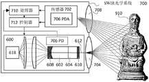
现在参考图1B及图1C,它们示意性地以图解说明根据一些实施例的编号为100’及100”的诸多其它SWIR成像系统。像系统100一样,系统100’包括一有源照明源102A及接收器110。在一些实施例中,成像系统100、100’及100”还包括控制器112及图像处理器114。在一些实施例中,接收器110的输出的处理可以由图像处理器114进行,并且附加地或替代地由一外部图像处理器(未被示出)进行。多个成像系统100’及100”可以是成像系统100的诸多变体。关于系统100被讨论的任何构件或功能可以在系统100’及100”中的任何一种中被实现,反之亦然。Reference is now made to FIGS. 1B and 1C, which schematically illustrate a number of other SWIR imaging systems numbered 100' and 100" in accordance with some embodiments. Like
控制器112是一计算装置(computing device)。在一些实施例中,控制器112的诸多功能在照明源102及接收器110内被提供,并且不需要控制器112作为一单独的构件。在一些实施例中,成像系统100’及100”的控制由控制器112、照明源102及接收器110共同作用而被进行。附加地或替代地,在一些实施例中,成像系统100’及100”的控制可以由一外部控制器诸如一车辆电子控制单元(ECU)120(其可能属于已被安装所述成像系统的一车辆)进行。The
照明源102被配置为在所述电磁光谱的红外(IR)区域中发射一光脉冲106。更具体地,光脉冲106在所述SWIR光谱带中,包括在大约1.3μm至3.0μm的一范围内的波长。
在一些实施例中,诸如在图1B中示出的,所述照明源(现在被标记为102A)是一有源Q开关激光器(或“有源Q型开关”激光器),其包括一增益介质(gain medium)122、一泵(pump)124、多个镜(未被示出)及一有源QS元件126A。在一些实施例中,QS元件126A是一调制器(modulator)。在由泵124对所述增益介质122进行电子式或光学式泵送(pumping)后,一光脉冲通过有源触发QS元件126A被释放。In some embodiments, such as shown in Figure IB, the illumination source (now labeled 102A) is an active Q-switched laser (or "active Q-switched" laser) that includes a gain medium (gain medium) 122, a pump 124, mirrors (not shown), and an
在一些实施例中,诸如在图1C中被示出的,照明源102P是一P-QS激光器,所述P-QS激光器包括增益介质122、泵124、多个镜(未示出)及一SA126P。在一“无源QS(passive QS)”光脉冲被释放后,SA 126P允许所述激光腔存储光能(来自由泵124泵送的增益介质122),直到在SA 126P中达到一饱和水平。为了检测所述无源QS脉冲的释放,一QS脉冲光电检测器128被耦合到照明源102P。在一些实施例中,QS脉冲光电检测器128是一锗PD。来自QS脉冲光电检测器128的所述信号被用来触发在接收器110中的接收过程,使得接收器110将在适于要被成像的目标104距离的一时间段后被激活。所述时间段被派生如以下参考图3B、图3C、图4B及图4C进一步描述的。In some embodiments, such as shown in FIG. 1C, the
在一些实施例中,来自照明源102的激光脉冲持续时间在从100ps到1微秒的范围内。在一些实施例中,激光脉冲能量在从10微焦耳到100毫焦耳的范围内。在一些实施例中,所述激光脉冲周期为100微秒的量级。在一些实施例中,所述激光脉冲周期在从1微秒到100毫秒的范围内。In some embodiments, the laser pulse duration from
增益介质122以一晶体的形式或替代地以一陶瓷形式被提供。可以用于增益介质122的多个材料的多个非限制性示例包括:Nd:YAG、Nd:YVO4、Nd:YLF、Nd:Glass、Nd:GdVO4、Nd:GGG、Nd:KGW、Nd:KYW、Nd:YALO、Nd:YAP、Nd:LSB、Nd:S-FAP、Nd:Cr:GSGG、Nd:Cr:YSGG、Nd:YSAG、Nd:Y2O3、Nd:Sc2O3、Er:Glass、Er:YAG,依此类推。在一些实施例中,所述增益介质的多个掺杂水平可以基于对一特定增益的需求被改变。多个SA 126P的多个非限制性示例包括:Co2+:MgAl2O4、Co2+:尖晶石(Spinel)、Co2+:硒化锌(ZnSe)与其它掺钴晶体、V3+:YAG、被掺杂的玻璃、量子点、半导体SA镜(SESAM)、Cr4+YAG SA,诸如此类。P-QS激光器102P可以被实现的诸多附加方式参照图6至图11被讨论,关于一激光器600被讨论的任何变体也可以比照适用照明源102P。Gain medium 122 is provided in the form of a crystal or alternatively in a ceramic form. Numerous non-limiting examples of various materials that may be used for gain medium 122 include: Nd:YAG, Nd:YVO4, Nd:YLF, Nd:Glass, Nd:GdVO4, Nd:GGG, Nd:KGW, Nd:KYW , Nd:YALO, Nd:YAP, Nd:LSB, Nd:S-FAP, Nd:Cr:GSGG, Nd:Cr:YSGG, Nd:YSAG, Nd:Y2O3, Nd:Sc2O3, Er:Glass, Er:YAG ,So on and so forth. In some embodiments, the multiple doping levels of the gain medium can be varied based on the requirements for a particular gain. Numerous non-limiting examples of
关于照明源102,要被注意的是,具备足够功率及足够短脉冲的脉冲激光比无脉冲照明更难获得且更昂贵,尤其是在基于太阳吸收的人眼安全SWIR辐射被需要时。With regard to the
接收器110可以包括:一个或多个锗PD 118及接收器光学器件116。在一些实施例中,接收器110包括多个锗PD 118的一2D阵列。接收器110被选择以使其对红外辐射敏感,所述红外辐射至少包括由照明源102发射的波长,从而致使得所述接收器可以从反射辐射108形成所述被照明的目标104的意象(imagery)。The receiver 110 may include: one or more germanium PDs 118 and receiver optics 116 . In some embodiments, receiver 110 includes a 2D array of germanium PDs 118 . The receiver 110 is selected to be sensitive to infrared radiation comprising at least the wavelengths emitted by the
接收器光学器件116可以包括:一个或多个光学元件,例如诸多镜或诸多透镜,其被布置成收集、集中及可选地过滤所述被反射的电磁辐射228,并将所述电磁辐射聚焦到接收器110的一焦平面上。The receiver optics 116 may include one or more optical elements, such as mirrors or lenses, arranged to collect, concentrate and optionally filter the reflected electromagnetic radiation 228 and focus the electromagnetic radiation to a focal plane of receiver 110.
接收器110响应于由代表所述照明场景的意象的一个或多个锗PD 118所检测的电磁辐射而生成多个电信号。由接收器110所检测的多个信号可以被传输到内部图像处理器114或一外部图像处理器(未被示出),以处理成所述目标104的一SWIR图像。在一些实施例中,接收器110被多次激活以创建“多个时间切片(time slices)”,每个时间片覆盖一特定距离范围。在一些实施例中,图像处理器114结合这些切片以创建具备更大视觉深度的单个图像,诸如由格鲁伯(Gruber)、托比亚斯(Tobias)等人提出的。“Gated2depth:来自门控图像的实时密集激光雷达(LIDAR)”,arXiv预印本arXiv:1902.04997(2019),在此全文引入作为参考。The receiver 110 generates a plurality of electrical signals in response to electromagnetic radiation detected by one or more germanium PDs 118 representing an image of the lighting scene. The signals detected by receiver 110 may be transmitted to
在汽车领域,由多个成像系统100’或100”生成的接收器110的视场(FOV)内的所述图像的目标104可以被处理,以提供各种驾驶员辅助及诸多安全功能,诸如:前向碰撞警告(FCW)、车道偏离警告(LDW)、交通标志识别(TSR)以及对相关实体诸如行人或迎面而来车辆的检测。所述被生成的图像也可以被显示给驾驶员,例如被投影在车辆挡风玻璃上的一平视显示器(HUD)上。附加地或替代地,多个成像系统100’或100”可以介接到一车辆ECU 120,以提供诸多图像或视频,以使得自动驾驶能够在低光照水平或恶劣的可见性条件下进行。In the automotive field, the
在诸多有源成像场景中,一光源譬如激光器与多个光接收器的一阵列被结合使用。由于所述锗PD在所述SWIR波段操作,因此在不超出人眼安全规定的情况下,高功率光脉冲是可行的。对于汽车场景中的实现方案,一典型的脉冲长度为~100纳秒(ns),尽管,在某些实施例中,也可以预期高达约1微秒的更长的脉冲持续时间。考虑到人眼的安全性,~300千瓦(KW)的一峰值脉冲功率是被允许的,但是当前的激光二极管实际上无法达到此水平。因此,在本系统中,所述高功率脉冲是由一QS激光器生成的。在一些实施例中,所述激光是一P-QS激光器,以进一步降低成本。在一些实施例中,所述激光器是有源QS。In many active imaging scenarios, a light source, such as a laser, is used in conjunction with an array of light receivers. Since the germanium PD operates in the SWIR band, high power optical pulses are feasible without exceeding eye safety regulations. For implementations in automotive scenarios, a typical pulse length is -100 nanoseconds (ns), although, in some embodiments, longer pulse durations of up to about 1 microsecond are also contemplated. Considering the safety of the human eye, a peak pulse power of ~300 kilowatts (KW) is permissible, but current laser diodes are practically incapable of reaching this level. Therefore, in the present system, the high power pulses are generated by a QS laser. In some embodiments, the laser is a P-QS laser to further reduce cost. In some embodiments, the laser is an active QS.
如本文被使用的,所述术语“目标(target)”意指任何的一被成像的实体、物体、区域或场景(an imaged entity,object,area,or scene)。在诸多汽车应用中的诸多目标的诸多非限制性示例包括诸多车辆、诸多行人、诸多物理障碍或其它物体。As used herein, the term "target" means any imaged entity, object, area, or scene. Non-limiting examples of targets in automotive applications include vehicles, pedestrians, physical obstacles, or other objects.
根据一些实施例,一种有源成像系统包括:一照明源,用于朝向一目标发射一辐射脉冲,从而引起从所述目标反射辐射,其中所述照明源包括一QS激光器;及一接收器,包括一个或多个锗PD,用于接收所述反射辐射。在一些实施例中,所述照明源在所述SWIR光谱带中操作。According to some embodiments, an active imaging system includes: an illumination source for emitting a pulse of radiation toward a target, causing reflection of radiation from the target, wherein the illumination source includes a QS laser; and a receiver , comprising one or more germanium PDs for receiving the reflected radiation. In some embodiments, the illumination source operates in the SWIR spectral band.
在一些实施例中,所述QS激光器是一有源QS激光器。在一些实施例中,所述QS激光器是一P-QS激光器。在一些实施例中,所述P-QS激光器包括一SA。在一些实施例中,所述SA被选自于由以下材料组成的群组:Co2+:MgAl2O4、Co2+:尖晶石、Co2+:ZnSe与其它掺钴晶体、V3+:YAG、掺杂的玻璃、量子点、半导体SA镜(SESAM)及Cr4+YAG SA。In some embodiments, the QS laser is an active QS laser. In some embodiments, the QS laser is a P-QS laser. In some embodiments, the P-QS laser includes an SA. In some embodiments, the SA is selected from the group consisting of: Co2+:MgAl2O4, Co2+:spinel, Co2+:ZnSe and other cobalt-doped crystals, V3+:YAG, doped glass, quantum point, semiconductor SA mirror (SESAM) and Cr4+YAG SA.
在一些实施例中,所述系统还包括一QS脉冲光电检测器,用于检测由所述P-QS激光器发射的一辐射脉冲。在一些实施例中,所述接收器被配置为在足以使所述辐射脉冲行进到一目标并返回到所述接收器的一时间被激活。在一些实施例中,所述接收器在一积分时间被激活,在所述积分时间内,所述锗PD的暗电流功率不超过所述锗PD的所述kTC噪声功率。In some embodiments, the system further includes a QS pulse photodetector for detecting a radiation pulse emitted by the P-QS laser. In some embodiments, the receiver is configured to be activated for a time sufficient for the radiation pulse to travel to a target and back to the receiver. In some embodiments, the receiver is activated for an integration time during which the dark current power of the germanium PD does not exceed the kTC noise power of the germanium PD.
在一些实施例中,所述接收器响应于由多个锗PD接收的所述反射辐射而生成多个电信号,其中所述多个电信号代表由所述辐射脉冲照射的所述目标的意象。在一些实施例中,所述多个电信号由一内部图像处理器或一外部图像处理器中的一个处理成所述目标的一图像。在一些实施例中,所述目标的所述图像被处理以提供前向碰撞警告、车道偏离警告、交通标志识别以及对行人或迎面而来车辆的检测中的一种或多种。In some embodiments, the receiver generates a plurality of electrical signals in response to the reflected radiation received by the plurality of germanium PDs, wherein the plurality of electrical signals represent an image of the target illuminated by the radiation pulses . In some embodiments, the plurality of electrical signals are processed into an image of the object by one of an internal image processor or an external image processor. In some embodiments, the image of the target is processed to provide one or more of forward collision warning, lane departure warning, traffic sign recognition, and detection of pedestrians or oncoming vehicles.
根据诸多另外的实施例,一种用于进行有源成像的方法包括步骤:通过一照明源释放一光脉冲,所述照明源包括一有源QS激光器;以及在足以使所述光脉冲行进到一目标并返回到所述QS激光器的时间后,在一有限的时间段内激活一接收器,所述接收器包括一个或多个锗PD,以接收从所述目标被反射的一反射光脉冲(reflected light pulse)。在一些实施例中,所述照明源在短波红外(SWIR)光谱带中操作。在一些实施例中,所述有限的时间段等于一积分时间,在所述积分时间期间,所述锗PD的暗电流功率不超过所述锗PD的一kTC噪声功率。According to various further embodiments, a method for active imaging includes the steps of: releasing a light pulse by an illumination source, the illumination source including an active QS laser; and traveling the light pulse at a sufficient time to travel to After a target and time back to the QS laser, activate a receiver for a limited period of time, the receiver comprising one or more germanium PDs, to receive a reflected light pulse reflected from the target (reflected light pulse). In some embodiments, the illumination source operates in the short wave infrared (SWIR) spectral band. In some embodiments, the limited period of time is equal to an integration time during which the dark current power of the germanium PD does not exceed a kTC noise power of the germanium PD.
在一些实施例中,所述接收器响应于由所述多个锗PD接收的所述反射光脉冲而生成所述多个电信号,其中所述多个电信号代表由所述光脉冲照射的所述目标的意象。在一些实施例中,所述多个电信号由一内部图像处理器或一外部图像处理器中的一个处理成所述目标的一图像。在一些实施例中,所述目标的所述图像被处理以提供前向碰撞警告、车道偏离警告、交通标志识别以及对行人或迎面而来车辆的检测中的一种或多种。In some embodiments, the receiver generates the plurality of electrical signals in response to the reflected light pulses received by the plurality of germanium PDs, wherein the plurality of electrical signals represent light pulses illuminated by the light pulses image of the target. In some embodiments, the plurality of electrical signals are processed into an image of the object by one of an internal image processor or an external image processor. In some embodiments, the image of the target is processed to provide one or more of forward collision warning, lane departure warning, traffic sign recognition, and detection of pedestrians or oncoming vehicles.
根据诸多另外的实施例,一种用于进行有源成像的方法包括步骤:泵送一P-QS激光器,所述P-QS激光器包括一SA,以在所述SA饱和时引起一光脉冲的释放;通过一QS脉冲光电检测器检测所述光脉冲的所述释放;基于所述被检测的光脉冲释放,在足以使所述光脉冲行进到一目标并返回到所述QS激光器的时间后,在一有限的时间段内激活一接收器,所述接收器包括一个或多个锗PD,以接收所述反射光脉冲。在一些实施例中,所述QS激光器在短波红外(SWIR)光谱带中操作。According to various further embodiments, a method for active imaging includes the step of pumping a P-QS laser, the P-QS laser including a SA, to induce a pulse of light when the SA is saturated release; detecting said release of said light pulse by a QS pulse photodetector; based on said detected light pulse release, after a time sufficient for said light pulse to travel to a target and back to said QS laser , activating a receiver comprising one or more germanium PDs for a limited period of time to receive the reflected light pulses. In some embodiments, the QS laser operates in the shortwave infrared (SWIR) spectral band.
在一些实施例中,所述SA被选自于Co2+:MgAl2O4、Co2+:尖晶石、Co2+:ZnSe、其它被掺钴晶体、V3+:YAG、被掺杂的玻璃、量子点、半导体SA镜(SESAM)及Cr4+YAG SA。在一些实施例中,所述有限的时间段等于一积分时间,在所述积分时间期间,所述锗PD的暗电流功率不超过所述锗PD的所述kTC噪声功率。In some embodiments, the SA is selected from Co2+:MgAl2O4, Co2+:spinel, Co2+:ZnSe, other cobalt-doped crystals, V3+:YAG, doped glass, quantum dots, semiconductor SA mirrors ( SESAM) and Cr4+YAG SA. In some embodiments, the limited period of time is equal to an integration time during which the dark current power of the germanium PD does not exceed the kTC noise power of the germanium PD.
在一些实施例中,所述接收器响应于由所述多个锗PD接收的所述反射光脉冲而生成多个电信号,其中所述多个电信号代表由所述光脉冲照射的所述目标的意象。在一些实施例中,所述多个电信号由一内部图像处理器或一外部图像处理器中的一个处理成所述目标的一图像。在一些实施例中,所述目标的所述图像被处理以提供前向碰撞警告、车道偏离警告、交通标志识别以及对行人或迎面而来车辆的检测中的一种或多种。In some embodiments, the receiver generates a plurality of electrical signals in response to the reflected light pulses received by the plurality of germanium PDs, wherein the plurality of electrical signals are representative of the light pulses illuminated by the light pulses image of the target. In some embodiments, the plurality of electrical signals are processed into an image of the object by one of an internal image processor or an external image processor. In some embodiments, the image of the target is processed to provide one or more of forward collision warning, lane departure warning, traffic sign recognition, and detection of pedestrians or oncoming vehicles.
示例性实施例涉及一种用于使用多个基于锗的PD的高SNR有源SWIR成像的系统及方法。在一些实施例中,所述成像系统是一门控成像系统(gated imaging system)。在一些实施例中,所述脉冲照明源是一有源或P-QS激光器。Exemplary embodiments relate to a system and method for high SNR active SWIR imaging using multiple germanium-based PDs. In some embodiments, the imaging system is a gated imaging system. In some embodiments, the pulsed illumination source is an active or P-QS laser.
现在参考图3A、图3B及图3C,分别示出根据一些实施例的一有源SWIR成像系统的一操作方法的一流程图及多个示意图。在图3A中被示出的过程300是基于如参照图1B所描述的系统100’。在步骤302中,照明源102A的泵124被激活以泵送增益介质122。在步骤304中,有源QS元件126A沿一目标104的方向释放一光脉冲,所述目标104位于一距离为D处。在步骤306中,在时间=T,所述光脉冲冲击目标104并生成朝向系统100’及接收器110返回的反射辐射。在步骤308中,在等待一时间=T2后,接收器110被激活以接收所述反射辐射。所述返回传播延迟T2由所述脉冲从照明源102A到目标104的所述飞行时间(flight time)加上从目标104被反射的所述光信号的飞行时间组成。因此,对于与照明源102A及接收器110相距一距离“D”处的一目标104而言,T2是已知的。接收器110的所述激活周期Δt是基于所需的景深(DoV)被决定。所述DoV由2DoV=c*Δt给出,其中c是光速。一100ns的典型Δt提供一15米的景深。在步骤310中,所述反射辐射以一Δt的时间段被接收器110接收。来自接收器110的所述被接收的数据由图像处理器114(或外部图像处理器)处理以生成一接收图像(received image)。过程300可以在每个帧中被重复N次,其中一帧被定义为从接收器110被传输到图像处理器114(或一外部图像处理器)的所述数据集。在一些实施例中,N是在1与10,000之间。Referring now to FIGS. 3A , 3B, and 3C, a flowchart and schematic diagrams, respectively, of a method of operation of an active SWIR imaging system according to some embodiments are shown. The
现在参考图4A、图4B及图4C分别示出根据一些实施例的一有源SWIR成像系统的一示例性操作方法的一流程图及多个示意图。在图4中被示出的一过程400是基于如参考图1C所描述的系统100”。在步骤402中,照明源102P的泵124被激活以泵送增益介质122并使SA126P饱和。在步骤404中,在达到一饱和水平后,SA 126P沿一目标430的方向释放一光脉冲,所述目标430位于一距离为D处。在步骤406中,QS脉冲光电检测器128检测所述被释放光脉冲。在步骤408中,在时间=T,所述光脉冲冲击目标430,并生成朝向系统100”及接收器110返回的反射辐射。在步骤410中,在等待由QS脉冲光电检测器128所检测的一被释放光脉冲后的一时间=T2后,接收器110被激活以接收所述反射辐射。所述返回传播延迟T2包括从照明源102P到目标430的脉冲的飞行时间加上从目标430被反射的光信号的飞行时间。因此,对于与照明源102P及接收器110相距一距离“D”处的一目标430而言,T2是已知的。所述Δt的激活周期是根据所需的景深(DoV)被决定。在步骤412中,接收器110以一Δt的时间段接收所述反射辐射。来自接收器110的所述被接收的数据由图像处理器114(或由外部图像处理器)处理以生成一接收图像。过程400可以在每个帧中被重复N次。在一些实施例中,N是在1与10,000之间。Referring now to FIGS. 4A , 4B, and 4C, a flowchart and various schematic diagrams, respectively, of an exemplary method of operation of an active SWIR imaging system according to some embodiments are shown. A
参照所有成像系统100、100’及100”,要被注意的是,那些成像系统中的任何一个都可以包括:读出电路,用以在所述积分时间后读出由每个锗PD收集的电荷的一累积,以提供所述相应PD的所述检测信号。这样,与LIDARs或其它深度传感器不同,所述读出过程可以在所述积分时间的震荡后被执行并且因此在所述信号从一大范围的多个距离不可逆地求和(irreversibly summed)后被执行。With reference to all of the
参照所有成像系统100、100’及100”,可选地,接收器110输出代表由多个锗PD中的每个在所述积分时间内累积的电荷的一检测信号组,其中所述检测信号组代表由至少一个SWIR辐射脉冲所照射的所述目标的意象。Referring to all of the
参照所有成像系统100、100’及100”,所述成像系统可以可选地至少一个衍射光学元件(DOE),所述衍射光学元件可操作以在朝向所述目标发射光前改善所述脉冲照明源的光的照明均匀性。如上所述,一高峰值功率脉冲光源102可能在所述FOV的不同部分上发出一不够均匀的照明分布。所述DOE(未被以图解说明)可以改善所述照明的均匀性以生成所述FOV的多个高质量图像。要被注意的是,在诸多激光雷达系统及其它深度传感器中通常不需要等效的照明均匀性,因此出于成本、系统复杂性、系统体积等原因,它们可能不包含诸多DOE元件。例如:在诸多LIDAR系统中,只要整个FOV接收到足够的照明度(高于允许以一最小所需距离检测目标的一阈值),在所述FOV中的某些区域是否比所述FOV的其它部分所接收的照明密度更多就无关紧要。所述系统100的DOE,如果被实施,则可以例如被用于减少诸多斑点效应。要被注意的是,诸多成像系统100、100’及100”还可以包括:用于将光从光源102引导到所述FOV的其它类型的光学器件,诸如诸多透镜、诸多镜、诸多棱镜、诸多波导等。With reference to all
参照所有成像系统100、100’及100”,控制器112可以可选地被操作以激活接收器110以顺序获取一系列门控图像,每个门控图像表示在一不同距离范围内的不同锗PD的检测信号,及一图像处理器可操作于将所述系列图像组合成单个二维图像。例如:一第一图像可以获取在0与50米(m)之间的来自所述成像传感器的光,一第二图像可以获取在50至100米之间的来自所述成像传感器的光,一第三图像可以获取在100至125米之间的来自所述成像传感器的光,并且图像处理器114可以组合多个2D图像为单个2D图像。这样,每个距离范围都以被累积的暗电流噪声被捕获,所述被累积的暗电流噪声仍小于由读出电路引入的所述读出噪声,以使用更多的光脉冲及更多的计算为代价。所述最终图像的每个像素的所述颜色值(譬如灰度值)可以根据所述多个门控图像中的各个像素的一功能(譬如所有值中的一最大值或一加权平均值)被决定。Referring to all
所有成像系统100、100’及100”,所述成像系统可以是一未冷却的基于锗的SWIR成像系统,可操作在超过50(米)m的一距离处以一20%的SWIR反射率(在相关光谱范围内)检测一1m x 1m的目标。All
参照所有成像系统100、100’及100”,脉冲照明源102可以是一QS激光器,所述QS激光器可操作以发射具有在10毫焦耳(millijoule)与100毫焦耳之间的脉冲能量的人眼安全的激光脉冲。虽然不是必须的,但是所述照明波长可以被选择以匹配一太阳吸收带(譬如所述照明波长可以在1.3微米(μm)与1.4μm之间。Referring to all
参照所有成像系统100、100’及100”,用于图像生成的每个锗PD的输出信号可以代表每个PD的单个标量(scalar)。参照所有成像系统100、100’及100”,每个PD可以输出一累积信号,所述累积信号代表一大范围的多个距离。例如:接收器110的一些、大多数或全部锗PD可以输出多个检测信号,所述多个检测信号代表从20m、40m及60m反射到相应PD的光中的每个。Referring to all
与许多已知技术系统相比,诸多成像系统100、100’及100”的另一个区别特征是,所述脉冲照明不被用于冻结物体在野外的快速运动(譬如与摄影闪光灯照明不同),并且同样被用于静态场景。与许多已知技术系统相比,诸多成像系统100、100’及100”的另一个区别特征是,与外部噪声相比,所述图像的所述门控并不是主要用以避免所述系统中的内部噪声,这对于某些已知技术(譬如阳光)而言是一麻烦事。Another distinguishing feature of
要被注意的是,以上关于诸多系统100、100’及100”被讨论的构件、特征、操作模式、系统架构及内部关系中的任何一个都可以在必要的情况下在以下被讨论的任何EO系统中被实现,诸如诸多系统700、1300、1300’、1600、1600’、1700、1800、1900、2300及3600。It is to be noted that any of the components, features, modes of operation, system architectures and internal relationships discussed above with respect to the
图5是以图解说明根据本公开主题的诸多示例的一种用以在一EO系统的一FOV中生成诸多物体的诸多SWIR图像的方法500的一流程图。参考关于先前附图阐述的诸多示例,方法500可以由诸多成像系统100、100’及100”中的任何一个执行。要被注意的是,方法500也可以由描述如下的任何有源成像系统(诸如诸多系统700、1300、1300’、1600、1600’、1700、1800、1900、2300及3600)实现。5 is a flowchart illustrating a
方法500从朝向所述FOV发射至少一个照明脉冲的一步骤(或“阶段”)510开始,从而引起SWIR辐射从至少一个目标反射。在下文中,“步骤(step)”及“阶段(stage)”可被互换使用。可选地,所述一个或多个脉冲可以是高峰值功率脉冲。例如:与单个脉冲相比,多个照明脉冲可能需要被使用,以实现一总体上更高的照明水平(an overall higher level ofillumination)。参考诸多附图的诸多示例,步骤510可以可选地由控制器112执行。
一步骤520包括由一成像接收器触发连续信号获取的启动,所述成像接收器包括多个锗PD(在以上关于接收器110被讨论的意义上),所述接收器110可操作以检测所述被反射的SWIR辐射。步骤520的连续信号获取意谓所述电荷被连续且不可逆地收集(即,不可能获悉在任何中间时间收集到什么水平的电荷),而且不是以小增量方式收集。步骤520的所述触发可以在步骤510前被执行(譬如:如果所述检测阵列需要一加速时间),与步骤510同时被执行,或者在步骤510结束后(譬如在与系统相距一非零距离处开始检测)被执行。参考附图的示例,步骤520可以可选地由控制器112执行。A step 520 includes triggering the initiation of continuous signal acquisition by an imaging receiver comprising a plurality of germanium PDs (in the sense discussed above with respect to receiver 110) operable to detect the the reflected SWIR radiation. Continuous signal acquisition of step 520 means that the charge is collected continuously and irreversibly (ie, it is impossible to know what level of charge is collected at any intermediate time), and not in small increments. The triggering of step 520 may be performed before step 510 (eg, if the detection array requires an acceleration time), concurrently with
步骤530在触发步骤520后开始,并且包括对于多个锗PD中的每个进行收集,以作为所述触发的一结果,至少由所述SWIR反射辐射冲击在所述相应的锗PD上引起的电荷、大于50μA/cm2的暗电流、有关积分时间的暗电流噪声及无关积分时间的读出噪声。参考附图的示例,步骤530可以可选地由接收器110执行。Step 530 begins after triggering step 520 and includes collecting for each of a plurality of germanium PDs as a result of said triggering at least caused by said SWIR reflected radiation impinging on said corresponding germanium PD Charge, dark current greater than 50 μA/cm2 , dark current noise related to integration time and readout noise independent of integration time. Referring to the example of the figures, step 530 may optionally be performed by the receiver 110 .
步骤540包括:当由于暗电流噪声而被收集的电荷量仍低于由于累积无关时间的读出噪声而被收集的电荷量时,触发停止所述电荷的收集。所述积分时间是步骤530到步骤540停止为止的持续时间。参考附图的示例,步骤540可以可选地由控制器112执行。Step 540 includes triggering to stop the collection of charges when the amount of charge collected due to dark current noise is still lower than the amount of charge collected due to accumulated time-independent readout noise. The integration time is the duration of step 530 until step 540 stops. Referring to the example of the figures, step 540 may optionally be performed by the
一步骤560在步骤540结束后被执行,并且步骤560包括基于由多个锗PD中的每个收集的电荷水平以生成所述FOV的一图像。如前述关于诸多成像系统100、100’及100”,在步骤560中被生成的所述图像是没有深度信息的一2D图像。参考附图的示例,步骤560可以可选地由成像处理器114执行。A
可选地,作为步骤540的一结果的停止收集可以是接着可选的步骤550,由读出电路读取与所述多个锗PD中的每个锗PD所收集的电荷量相关的一信号,放大所述读取的信号,并提供所述被放大的信号(可选地,在进一步处理后)到一图像处理器,所述图像处理器执行如步骤560的所述图像的所述生成。参照附图的示例,步骤550可以可选地由所述读出电路(未被图解说明如上,但是可以等效于如下讨论的任何读出电路,诸如一读出电路1610、2318及3630)执行。要被注意的是,步骤550是可选的,因为从所述多个锗PS中读出所述诸多检测结果的其它合适的方法可以被实现。Optionally, the cessation of collection as a result of step 540 may be followed by optional step 550 of reading, by a readout circuit, a signal related to the amount of charge collected by each germanium PD of the plurality of germanium PDs. , amplify the read signal, and provide the amplified signal (optionally, after further processing) to an image processor that performs the generation of the image as in
可选地,多个锗PD中的每个输出的信号是一标量,表示从20米被反射的光、从40米被反射的光及从60米被反射的光量。Optionally, the signal output by each of the plurality of germanium PDs is a scalar representing the amount of light reflected from 20 meters, light reflected from 40 meters, and light reflected from 60 meters.
可选地,步骤560的所述生成可以包括:基于对于所述多个锗PD中的每个所读取的一标量值以生成所述图像。可选地,步骤510的所述发射可以包括:通过使脉冲激光照明(通过一个或多个激光器)穿过至少一个衍射光学元件(DOE),并将所述被削弱的光发射到所述FOV,以增加脉冲激光照明的照明均匀性。可选地,所述暗电流大于每锗PD为50皮安(picoampere)。可选地,所述多个锗PD是多个硅锗PD(Si-Ge PDs),每个硅锗PD都包括硅及锗。可选地,所述发射通过至少一个有源QS激光器被进行。可选地,所述发射通过至少一个P-QS激光器被进行。可选地,所述收集是当所述接收器在高于30℃的一温度下操作时被执行,并且处理所述FOV的所述图像以检测在50米与150米之间的多个范围内的多个车辆及多个行人。可选地,所述发射包括以小于1米的一距离发射具有在10毫焦耳与100毫焦耳之间的脉冲能量的多个照明脉冲到一人的未被保护的眼睛中,而不损害眼睛。Optionally, the generating of
如前述关于诸多有源成像系统100、100’及100”,几个门控图像可以被组合为单个图像。可选地,方法500可以包括:重复多次发射、触发、收集及停止(emitting,triggering,collecting and ceasing)的顺序;触发在每个顺序的来自光发射的不同时间的所述采集。在每个顺序,方法500可以包括:从所述接收机读取一检测值,所述检测值用于对应大于2米(譬如2.1米、5米、10米、25米、50米、100米)的不同距离范围的所述多个锗PD中的每个锗PD。在这样的一情况下,在步骤560中的所述图像的所述生成包括基于以不同顺序从不同锗PD读取的所述多个检测值以生成单个二维图像。要被注意的是,由于仅有几个图像被拍摄,所以所述多个门控图像不是稀疏的(即,在全部或大多数门控图像中,存在许多像素的检测值)。还要被注意的是,所述多个门控图像可以具有重叠的距离范围。例如:一第一图像可以代表距离范围为0至60米,一第二图像可以代表距离范围为50至100米,一第三图像可以代表距离范围为90至120米。As previously described with respect to the many
图6至11C演示诸多SWIR电光(EO)系统及诸多P-QS激光器可以在这种系统中被使用,以及诸多用于这种激光器的操作及制造的方法。Figures 6 through 11C demonstrate that SWIR electro-optic (EO) systems and P-QS lasers can be used in such systems, as well as methods for the operation and manufacture of such lasers.
图10是以图解说明根据本公开主题的诸多示例的SWIR光学系统700的一示例的一示意性功能框图。系统700至少包括P-QS激光器600,但是也可以如图10所示包括诸多附加部件,诸如一传感器702,可操作以感测来自系统700的所述FOV的反射光,尤其是从诸多外部物体910被反射的激光器600的反射照明。10 is a schematic functional block diagram illustrating an example of a SWIR
参照其它示例,传感器702可以被实现为本公开中被讨论的成像接收器、PDA或诸多光电检测装置,诸如诸多构件110、1300、1300’、1600、1600’、1700、1800、1900、2302及3610。Referring to other examples, sensor 702 may be implemented as an imaging receiver, PDA, or photodetection devices discussed in this disclosure, such as
一处理器710,可操作以处理传感器702的所述诸多感测结果。所述处理的所述输出可以是所述FOV的一图像、所述FOV的一深度模型、所述FOV的一个或多个部分的光谱分析、在所述FOV中的诸多被识别物体的信息、在所述FOV上的光统计或任何其它类型的输出。参考诸多其它示例,处理器710可以被实现为在本公开中被讨论的诸多处理器中的任何一个,诸如诸多处理器114、1908、2304及3620。A processor 710 operable to process the plurality of sensing results of the sensor 702 . The output of the processing may be an image of the FOV, a depth model of the FOV, a spectral analysis of one or more portions of the FOV, information on identified objects in the FOV, Light statistics or any other type of output on the FOV. The processor 710 may be implemented as any of the processors discussed in this disclosure, such as the
一控制器712,可操作以控制激光器600及/或处理器710的活动。例如:控制器712可以包括:控制处理器710及/或激光器600的时机、同步及其它操作参数。参照诸多其它示例,控制器712可以被实现为在本公开中被讨论的诸多其它控制器中的任何一个,诸如控制器112、1338、2314及3640。A controller 712 operable to control the activity of the
可选地,系统700可以包括:对所述激光的波长敏感的一SWIR PDA 706。这样,SWIR光学系统可以用作一有源SWIR摄像机、SWIR飞行时间(ToF)传感器、SWIR光检测及测距(LIDAR)传感器等。所述ToF传感器可能对所述激光的波长敏感。可选地,所述PDA可以是对由激光器600发射的诸多SWIR频率敏感的一基于CMOS的PDA,诸如由以色列的特拉维夫的趣眼有限公司(TriEye LTD)设计及制造的一基于CMOS的PDA。Optionally,
可选地,系统700可以包括:一处理器710,用于处理来自所述SWIR PDA(或系统700的任何其它光敏传感器)的检测数据。例如:所述处理器可以处理所述检测信息,以提供系统700的一视场(FOV)的一SWIR图像,以检测在所述FOV中的诸多物体,诸如此类。可选地,所述SWIR光学系统可以包括:一飞行时间(ToF)SWIR传感器及一控制器,所述飞行时间(ToF)SWIR传感器对所述激光的所述波长敏感,所述控制器可操作以将所述ToF SWIR传感器及所述P-QS SWIR激光器的操作同步以检测所述SWIR光学系统的视野中的至少一个物体的一距离。可选地,系统700可以包括:控制器712,所述控制器712可操作以控制激光器600或系统的诸多其它构件诸如光电检测器阵列(譬如焦平面阵列,FPA)的一操作的一个或多个方面。例如:所述激光的一些参数可以由所述控制器控制,包括时机、持续时间、强度、聚焦(timing,duration,intensity,focusing),诸如此类。尽管不是必须的,但是所述控制器可以基于所述PDA的诸多检测结果(直接地,或者基于所述处理器的处理)以控制所述激光器的操作。可选地,所述控制器可以是可操作以控制所述激光泵或其它类型的光源以影响所述激光的诸多激活参数。可选地,所述控制器可以是可操作以动态地改变所述脉冲重复率。可选地,所述控制器可以是可操作以控制所述光整形光学器件的动态修改,例如:用于改善视场中的诸多特定区域中的一信噪比(SNR)。可选地,所述控制器可以是可操作以控制所述照明模块以动态地改变脉冲能量及/或持续时间(譬如以诸多其它P-QS激光器可能的相同方式,诸如改变泵送激光的聚焦等)。Optionally,
进一步并且可选地,系统700可以包括:温度控制(譬如无源温度控制、有源温度控制),用于总体上控制所述激光或者其一个或多个构件(譬如所述泵二极管)的一温度。这样的温度控制可以包括:例如一热电冷却器(TEC)、一风扇、一散热器、在泵二极管下的电阻加热器,依此类推。Further and alternatively,
进一步并且可选地,系统700可以包括:被用于漂白GM 602及SA 604中的至少一个的另一激光器。可选地,系统700可以包括:一内部光敏检测器(譬如一个或多个PD,像PDA706),所述内部光敏检测器可操作以测量由激光器600(譬如如上所述的PD 226)生成一脉冲的一时间。在这样的一情况下,控制器740可操作以基于从内部光敏检测器706获得的时机信息发出一触发信号到PDA 706(或其它类型的照相机或传感器702),所述PDA 706检测来自系统700的视场中的诸多物体的激光的光的反射。Further and optionally,
在上述光谱范围(1.3至1.5μm)内需要大量激光器的主要行业是用于光学数据存储的电子行业,这使得所述二极管激光器的成本降低至每装置、每瓦为数美元甚至更低。但是,这些激光器不适用于其它行业,例如汽车行业,这些行业要求激光具备相当高的峰值功率及光束亮度,并且将在恶劣的环境条件下被使用。A major industry requiring large numbers of lasers in the above-mentioned spectral range (1.3 to 1.5 μm) is the electronics industry for optical data storage, which brings the cost of such diode lasers down to a few dollars per device, per watt or even lower. However, these lasers are not suitable for other industries, such as the automotive industry, which require lasers with fairly high peak power and beam brightness, and will be used in harsh environmental conditions.
应当指出的是,关于被认为是所述SWIR光谱的一部分的波长范围,尚无科学共识。然而,出于本公开的目的,所述SWIR光谱包括电磁辐射,所述电磁辐射的波长大于可见光谱的波长,并且所述电磁辐射至少包括在1300与1500nm之间的光谱范围。It should be noted that there is no scientific consensus on the wavelength range considered to be part of the SWIR spectrum. However, for the purposes of this disclosure, the SWIR spectrum includes electromagnetic radiation having wavelengths greater than those of the visible spectrum, and including at least the spectral range between 1300 and 1500 nm.
尽管不限于这种用途,但是一个或多个P-QS激光器600可以被用作成像系统100、100’及100”中的任何一个的照明源102。激光器600可以被用在需要脉冲照明的SWIR范围内的任何其它EO系统中,例如诸多激光雷达、诸多光谱仪、诸多通信系统,诸如此类。要被注意的是,所述诸多被提出的激光器600及用于制造这种激光器的诸多方法允许以相对较低的产出成本进行大批量制造在所述SWIR光谱范围内操作的激光器。Although not limited to this use, one or more P-
P-QS激光器600至少包括一晶体增益介质(crystalline gain medium)602(在下文中增益介质也被称为“GM”)、一晶体SA 604及一光腔606,上述结晶材料在所述光腔606中被限制,以允许光在增益介质602中进行传播,以增强趋向生成一激光光束612(譬如在图8中示出)。所述光腔也被众所周知为所述术语“光学谐振器(optical resonator)”及“谐振腔(resonating cavity)”,并且所述光腔包括一高反射率镜608(也称为“高反射器(highreflector)”)及一输出耦合器610。以下被讨论的是几种不同类型的结晶材料的独特且新颖的组合,并且使用多种制造技术以制造激光器,从而允许大批量制造价格合理的所述SWIR光谱范围的诸多激光器。出于本公开内容的简洁的原因,在此不提供关于P-QS激光器的本领域中公知的一般细节,但是这些细节可以从各种各样的资源中容易地获得。如本领域中已知的,所述激光器的所述可饱和吸收体(saturable absorber)用作所述激光器的所述Q开关(Q-switch)。所述术语“结晶材料(crystalline material)”广泛地包括单晶形式或多晶形式的任何材料。The P-
所述被连接的晶体增益介质及晶体SA的尺寸可以取决于设计一特定P-QS激光器600的目的。在一非限制性示例中,所述SA及所述GM的一结合长度是在5与15毫米之间。在一非限制性示例中,所述SA及所述GM的所述结合长度是在2与40毫米之间。在一非限制性示例中,所述SA及所述GM的所述组合的一直径(譬如如果是一圆柱体,或被局限在一虚构的此类圆柱体中)是在2与5毫米之间。在一非限制性示例中,SA及GM的所述组合的一直径是在0.5与10毫米之间。The dimensions of the connected crystal gain medium and crystal SA may depend on the purpose for which a particular P-
P-QS激光器600包括一增益介质结晶材料(GMC),所述增益介质结晶材料被刚性连接到一SA结晶材料(SAC)。所述刚性耦合可以用本领域中已知的任何一种方式被实现,诸如使用粘合剂、扩散粘结、复合晶体粘结、生长一个在另一个的上部,诸如此类。然而,如下所述,以一陶瓷形式的刚性连接的结晶材料可以使用简单且廉价的方法被实现。要被注意的是,所述GMC及所述SAC材料可以彼此直接刚性连接,但是可以可选地经由一中间物体(譬如另一晶体)彼此刚性连接。在一些实施方案中,所述增益介质及所述SA两者可以在单片结晶材料上被实现,通过将不同掺杂剂(譬如下文关于SAC材料及GMC被讨论的那些)掺杂在单片结晶材料的不同部分,或通过共掺杂单片结晶材料,将两种掺杂剂(譬如共掺杂有N3+及V3+的一陶瓷YAG)掺杂相同体积的结晶材料。可选地,所述增益介质可以在一单晶饱和吸收基板(single crystal saturable absorbing substrate)上生长(譬如使用液相外延,LPE)。要被注意的是,在如下的公开中被广泛讨论的分离的GMC材料及SA结晶材料,掺杂有两种掺杂剂的单片陶瓷结晶材料也可以被比照使用于任何后列的实现方案中。P-
图7A、图7B及图7C是以图解说明根据当前公开的主题的P-QS激光器600的诸多示例的诸多示意性功能框图。在图7A中,所述两种掺杂剂被实现在所述普通结晶材料614的两个部分上(既充当GM又充当SA),而在图7B中,所述两种掺杂剂被实现在普通结晶材料614(在被图解说明的情况下-所述普通晶体的整体)的普通体积上被可互换地实现。可选地,所述GM及所述SA可以在被掺杂有钕及至少一种其它材料的单片结晶材料上被实现。可选地(譬如如图7C所示),输出耦合器610及高反射率镜608中的任何一者或两者可以被直接胶合到所述多种结晶材料(譬如所述GM或所述SA,或将两者结合的一晶体)中的一种。7A, 7B, and 7C are various schematic functional block diagrams illustrating examples of P-
SAC及GMC中的至少一种是一陶瓷结晶材料,所述陶瓷结晶材料是以一陶瓷形式(譬如一多晶形式)的相关结晶材料(譬如被掺杂的钇铝石榴石,YAG,被掺杂钒)。具有一种(尤其是两种)陶瓷形式的结晶材料允许更高数量及更低成本的生产。例如:代替在一缓慢且有限的过程中生长单独的单晶材料,通过粉末烧结(即,压实并可能加热一种粉末以形成一固体质量)、低温烧结、真空烧结,诸如此类,多晶材料可以被制造。诸多结晶材料(SAC或GMC)中的一种可以被烧结在另一种的上部,从而消除进行复杂且昂贵的工艺程序,诸如抛光、扩散粘结或表面活化粘结。可选地,所述GMC及SAC中的至少一个是多晶的。可选地,所述GMC及所述SAC都是多晶的。At least one of SAC and GMC is a ceramic crystalline material that is a related crystalline material (eg, doped yttrium aluminum garnet, YAG) in a ceramic form (eg, a polycrystalline form) doped with vanadium). Having a crystalline material in one (especially two) ceramic forms allows for higher quantity and lower cost production. For example: instead of growing individual single crystal materials in a slow and limited process, by powder sintering (ie, compacting and possibly heating a powder to form a solid mass), low temperature sintering, vacuum sintering, and the like, polycrystalline materials can be manufactured. One of the many crystalline materials (SAC or GMC) can be sintered on top of the other, eliminating the need to perform complex and expensive process procedures such as polishing, diffusion bonding or surface activated bonding. Optionally, at least one of the GMC and SAC is polycrystalline. Optionally, both the GMC and the SAC are polycrystalline.
提到所述GMC及所述SAC的诸多结晶材料的所述诸多组合可以被制成,这样的诸多组合可以包括:It is mentioned that the combinations of crystalline materials of the GMC and the SAC can be made, such combinations can include:
a.所述GMC是陶瓷掺钕的钇铝石榴石(Nd:YAG),并且所述SAC是(a)陶瓷掺三价钒的钇铝石榴石(V3+:YAG)或(b)一陶瓷掺钴结晶材料。可选地,所述陶瓷掺钴结晶材料可以是两价陶瓷掺钴结晶材料。在那些替代方案中,选自于上述群组的所述Nd:YAG及所述SAC两者均为陶瓷形式。一掺钴结晶材料是掺有钴的一结晶材料。诸多示例包括掺钴尖晶石(Co:钴或
b.所述GMC是陶瓷掺钕的钇铝石榴石(Nd:YAG),并且所述SAC是一非陶瓷SAC,选自于由以下材料组成的多个掺杂陶瓷材料的一群组:(a)掺三价钒的钇铝石榴石(V3+:YAG)及(b)掺钴结晶材料。可选地,所述掺钴结晶材料可以是掺二价钴结晶材料。在这样的一情况下,高反射率镜608及输出耦合器610被刚性连接到所述增益介质及所述SA,使得P-QS激光器600是一单片微芯片P-QS激光器。b. The GMC is a ceramic neodymium-doped yttrium aluminum garnet (Nd:YAG), and the SAC is a non-ceramic SAC selected from the group of doped ceramic materials consisting of: ( a) Vanadium-doped yttrium aluminum garnet (V3+ :YAG) and (b) cobalt-doped crystalline materials. Optionally, the cobalt-doped crystalline material may be a divalent cobalt-doped crystalline material. In such a case, the
c.所述GMC是陶瓷掺钕稀土元素结晶材料,并且所述SAC是一陶瓷结晶材料,选自于由以下组成的多个掺杂的结晶材料的一群组:(a)掺三价钒的钇铝石榴石(V3+:YAG)及(b)诸多掺钴结晶材料。可选地,所述钴掺杂结晶材料可以是二价钴掺杂结晶材料。尽管不是必须的,但是在此选项中,高反射率镜608及输出耦合器610可以可选地被刚性连接到所述增益介质及所述SA,使得P-QS激光器600是一单片微芯片P-QS激光器。c. The GMC is a ceramic neodymium doped rare earth element crystalline material, and the SAC is a ceramic crystalline material selected from the group of a plurality of doped crystalline materials consisting of: (a) trivalent vanadium doped of yttrium aluminum garnet (V3+ : YAG) and (b) many cobalt-doped crystalline materials. Optionally, the cobalt-doped crystalline material may be a divalent cobalt-doped crystalline material. Although not required, in this option, the
要被注意的是,在任何一种实现方案中,一种掺杂结晶材料可以掺杂有超过一种掺杂剂。例如:所述SAC可以掺杂有以上公开的主掺杂剂以及至少一种其它掺杂材料(譬如以显着更低的含量)。一种掺钕稀土元素结晶材料是一种结晶材料,所述结晶材料的晶胞(unit cell)包含一稀土元素(一明决定义的15种化学元素群组中的一种,包括15种镧系元素以及钪及钇),并且其掺杂有钕(譬如三重离子化钕)可替代在所述晶胞的一部分中的所述稀土元素。可以在本公开中被使用的掺钕稀土元素结晶材料的几个非限制性示例为:It is noted that, in either implementation, a doped crystalline material may be doped with more than one dopant. For example: the SAC may be doped with the primary dopant disclosed above and at least one other dopant material (eg, at significantly lower levels). A neodymium-doped rare earth element crystalline material is a crystalline material whose unit cell contains a rare earth element (one of a well-defined group of 15 chemical elements, including 15 lanthanum). and scandium and yttrium), and its doping with neodymium (eg triple ionized neodymium) may replace the rare earth elements in a portion of the unit cell. A few non-limiting examples of neodymium-doped rare earth element crystalline materials that may be used in the present disclosure are:
a.Nd:YAG(如上所述),掺钕钨酸钇钾(Nd:KYW)、掺钕氟化锂钇(Nd:YLF)、掺钕原钒酸钇(
b.掺钕原钒酸(
c.掺钕硼酸钪镧(Nd:LSB),其中的所述稀土元素为钪;c. Neodymium-doped scandium lanthanum borate (Nd:LSB), wherein the rare earth element is scandium;
d.其它掺钕稀土元素结晶材料可以被使用,其中的稀土元素可以是钇、钆、钪或任何其它稀土元素。d. Other neodymium-doped rare earth element crystalline materials may be used, wherein the rare earth element may be yttrium, gadolinium, scandium or any other rare earth element.
以下讨论应用于诸多GMC及诸多SAC的任何可选的组合。The following discussion applies to any optional combination of GMCs and SACs.
可选地,所述GMC被直接刚性连接到所述SAC。替代地,所述GMC及所述SAC可以被间接连接(譬如所述SAC及GMC中的每个经由一种或多种中间结晶材料的一群组及/或经由一种或多种其它对相关波长透明的固体材料被连接)。可选地,所述SAC及所述GMC中的一者或两者对相关波长是透明的。Optionally, the GMC is rigidly connected directly to the SAC. Alternatively, the GMC and the SAC may be indirectly connected (eg, each of the SAC and GMC is related via a group of one or more intermediate crystalline materials and/or via one or more other pairs wavelength-transparent solid materials are attached). Optionally, one or both of the SAC and the GMC are transparent to the relevant wavelength.
可选地,所述SAC可以是掺钴尖晶石(Co Co2+:MgAl2O4)。可选地,所述SAC可以是掺钴YAG(Co:YAG)。可选地,这可以使得钴及钕Nd能够共掺杂在相同YAG上。可选地,所述SAC可以是掺钴硒化锌(Co2+:ZnSe)。可选地,所述GMC可以是一陶瓷掺钴结晶材料。Optionally, the SAC may be cobalt-doped spinel (Co Co2+ :MgAl2O4). Alternatively, the SAC may be cobalt-doped YAG (Co:YAG). Optionally, this may enable co-doping of cobalt and neodymium Nd on the same YAG. Alternatively, the SAC may be cobalt-doped zinc selenide (Co2+ :ZnSe). Optionally, the GMC may be a ceramic cobalt-doped crystalline material.
可选地,所述SA的一初始透射率(
由所述激光发射的所述诸多波长取决于被使用在它的构造中的材料,尤其取决于所述GMC及所述SAC的材料及掺杂剂。诸多输出波长的一些示例包括在1,300nm及1,500nm范围内的诸多波长。一些更具体的示例包括1.32μm或约1.32μm(譬如1.32μm±3nm)、1.34μm或约1.34μm(譬如1.34μm±3nm)、1.44μm或约1.44μm(譬如1.44μm±3nm)。对这些光频率范围中的一者或多者敏感的一对应成像器可以被包括在SWIR光学系统700中(譬如如图10所示)。The wavelengths emitted by the laser depend on the materials used in its construction, especially the materials and dopants of the GMC and the SAC. Some examples of output wavelengths include wavelengths in the range of 1,300 nm and 1,500 nm. Some more specific examples include 1.32 μm or about 1.32 μm (eg, 1.32 μm ± 3 nm), 1.34 μm or about 1.34 μm (eg, 1.34 μm ± 3 nm), 1.44 μm or about 1.44 μm (eg, 1.44 μm ± 3 nm). A corresponding imager sensitive to one or more of these optical frequency ranges may be included in SWIR optical system 700 (eg, as shown in Figure 10).
图8及图9是以图解说明根据当前公开的主题的诸多示例的SWIR光学系统700的多个示意性功能图。如在这些图例中被示范的,激光器600除了如上讨论的那些构件之外,还可以包括:诸多附加的构件,诸如(但不限于):8 and 9 are various schematic functional diagrams illustrating a SWIR
a.一光源诸如一闪光灯616或一激光二极管618,所述激光二极管618用作所述激光器的一泵。参考前面的诸多示例,所述光源可以用作泵124。a. A light source such as a flash lamp 616 or a
b.聚焦光学器件620(譬如透镜),用于将光从所述光源(譬如618)聚焦到所述激光器600的光轴上。b. Focusing optics 620 (eg, a lens) for focusing light from the light source (eg, 618 ) onto the optical axis of the
c.一扩散器(diffuser)或其它光学器件622,用以在激光光束612离开光腔606后操纵激光光束612。c. A diffuser or
可选地,SWIR光学系统700可以包括:光学器件708,以将所述激光散布在一更宽的FOV上,以改善在所述FOV中的眼睛安全性问题。可选地,SWIR光学系统700可以包括:光学器件704,以收集来自所述FOV的反射激光并将它引导到所述传感器702上,例如:引导到光电检测器阵列(PDA)706上,参见图10。可选地,所述P-QS激光器600是一个二极管泵送的固态激光器(DPSSL)。Optionally,
可选地,P-QS激光器600包括至少一个二极管泵光源872及用于将所述二极管泵光源的光聚焦到所述光学谐振器(光腔)中的光学器件620。可选地,所述光源位于所述光轴上(作为一端泵)。可选地,所述光源可以被刚性地连接到高反射率镜608或SA 604,使得所述光源是一单片微芯片P-QS激光器的一部分。可选地,所述激光器的所述光源可以包括:一个或多个垂直腔表面发射激光器(VCSEL)阵列。可选地,P-QS激光器600包括至少一个VCSEL阵列及用于将所述VCSEL阵列的光聚焦到所述光学谐振器中的光学器件。由所述光源(譬如所述激光泵)发出的波长可能取决于所述激光中被使用的诸多结晶材料及/或诸多掺杂剂。可以由所述泵发射的一些示例性泵送波长包括:808nm或约808nm、869nm或约869nm、约九百多(nine hundred and some)nm。Optionally, the P-
所述激光的所述功率可能取决于它被设计的用途。例如:所述激光输出功率可以是在1W与5W之间。例如:所述激光输出功率可以是在5W与15W之间。例如:所述激光输出功率可以是在15W与50W之间。例如:所述激光输出功率可以是在50W与200W之间。例如:所述激光输出功率可以是高于200W。The power of the laser may depend on the use for which it is designed. For example, the laser output power may be between 1W and 5W. For example, the laser output power may be between 5W and 15W. For example, the laser output power may be between 15W and 50W. For example, the laser output power may be between 50W and 200W. For example: the laser output power may be higher than 200W.
QS激光器600是一脉冲激光器,并且可以具有不同的频率(重复率)、不同的脉冲能量,及不同的脉冲持续时间,这可以取决于它被设计的用途。例如:所述激光的一重复率可以是在10Hz与50Hz之间。例如:所述激光的一重复率可以是在50Hz与150Hz之间。例如:所述激光的一脉冲能量可以是在0.1mJ与1mJ之间。例如:所述激光的一脉冲能量可以是在1mJ与2mJ之间。例如:所述激光的一脉冲能量可以是在2mJ与5mJ之间。例如:所述激光的一脉冲能量可以高于5mJ。例如:所述激光的一脉冲持续时间可以是在10ns与100ns之间。例如:所述激光的一脉冲持续时间可以是在0.1μs与100μs之间。例如:所述激光的一脉冲持续时间可以是在100μs与1ms之间。所述激光的尺寸也可以改变,例如取决于它的部件的尺寸。例如:所述激光的尺寸可以是X乘X乘X,其中每个尺寸(

可选地,除了所述增益介质及所述SA之外,激光器600还可以包括:未掺杂YAG,用于防止热量累积在所述增益介质的一吸收区域中。所述未掺杂YAG可以可选地被成形为包围所述增益介质及所述SA的一圆柱体(譬如一同心圆柱体)。Optionally, in addition to the gain medium and the SA, the
图11A是以图解说明根据当前公开的主题的方法1100的一示例的一流程图。方法1100是一种用于制造用于一P-QS激光器的多个部件的方法,所述P-QS激光器例如但不限于上述P-QS激光器600。参考关于先前附图阐述的诸多示例,所述P-QS激光器可以是激光器600。要被注意的是,关于激光器600或关于其一构件被讨论的任何变体也可以对于在方法1100中被制造的所述P-QS激光器的诸多部件或关于其一对应的构件被实施,反之亦然。11A is a flow diagram illustrating an example of a
方法1100以将至少一种第一粉末塞入(inserting into)一第一模具中的步骤1102开始,所述步骤1102随后在方法1100中被处理以产出一第一结晶材料。所述第一结晶材料用作所述P-QS激光器的所述GM或所述SA。在一些实现方案中,所述激光器的所述增益介质首先被制造(譬如通过烧结的方式),然后所述SA被制造在所述先前制造的GM的顶部上(譬如通过烧结的方式)。在其它实现方案中,所述激光器的所述SA首先被制成,然后所述GM被制成在所述先前制造的SA的顶部上。在其它实现方案中,所述SA及所述GM被彼此独立地制成,并且被耦合以形成单个刚体。所述耦合可以作为加热、烧结或稍后的一部分被完成。
方法1100的步骤1104包括将至少一种第二粉末塞入一第二模具中,所述至少一种第二粉末与所述至少一种第一粉末不同。所述至少一种第二粉末稍后在方法1100中被处理,以产出一第二结晶材料。所述第二结晶材料用作所述P-QS激光器的所述GM或所述SA(以便所述SA及所述GM中的一者由所述第一结晶材料制成,另一功能性由所述第二结晶材料制成)。
所述第二模具可以与所述第一模具不同。替代地,所述第二模具可以与所述第一模具相同。在这样的一情况下,所述至少一种第二粉末可以被塞入,例如:在所述至少一种第一粉末的顶部上(或者如果已经制成,则在所述第一生坯的顶部上),在其旁边、在其周围,诸如此类。所述将至少一种第二粉末塞入所述至少一种第一粉末的相同模具(如果被实现)可以被执行在将所述至少一种第一粉末处理成一第一生坯前、在将所述至少一种第一粉末处理成所述后第一生坯,或在将所述至少一种第一粉末处理成所述第一生坯的过程中的某个时间。The second mold may be different from the first mold. Alternatively, the second mold may be the same as the first mold. In such a case, the at least one second powder may be inserted, for example, on top of the at least one first powder (or if already made, on top of the first green body) on top), beside it, around it, and so on. Said inserting of the at least one second powder into the same mold (if implemented) into the at least one first powder may be performed prior to processing the at least one first powder into a first green body, before processing the at least one first powder into a first green body. The at least one first powder is processed into the post first green body, or sometime during processing of the at least one first powder into the first green body.
所述第一粉末及/或所述第二粉末可包括被压碎的YAG(或任何其它前述材料,诸如尖晶石、

步骤1106在步骤1102后被执行,并且包括将在第一模具中的所述至少一种第一粉末压实以产出一第一生坯。步骤1104在步骤1108后被执行,其包括将在第二模具中的至少一种第二粉末压实,从而产出一第二生坯。如果在步骤1102及1104中将所述至少一种第一粉末及所述至少一种第二粉末塞入相同模具中,则可以在步骤1106及1108中同时进行所述诸多粉末的压实(譬如按压所述至少一种第二粉末,所述至少一种第二粉末转而压缩所述至少一种第一粉末紧靠所述模具),但这不是必须的。例如:步骤1104(以及因此也执行步骤1108)可以可选地在步骤1106的压缩后被执行。
步骤1110包括将所述第一生坯加热以产出(yield)一第一结晶材料。步骤1112包括将所述第二生坯以产出一第二结晶材料。在不同的实施例中,所述第一晶体的所述加热可以在步骤1106及1110中的每个以前、同时、部分同时或以后被执行。
可选地,在步骤1110处进行所述第一生坯的加热先于在步骤1108中(并且可能在步骤1104中)进行所述至少一种第二粉末的压实(并且还可能先于所述塞入)。所述第一生坯及所述第二生坯可以分别被加热(譬如在不同的时间、在不同的温度、对于不同的持续时间)。所述第一生坯及所述第二生坯可以一起被加热(譬如在相同烤箱中),或者在加热中彼此连接或不这样做。所述第一生坯及所述第二生坯可以经受不同的加热制度(heatingregimes),所述加热制度可以共享部分共加热,同时在加热制度的其它部分中被分别加热。例如:所述第一生坯及所述第二生坯中的一者或两个可以与另一生坯分开地加热,然后所述两个生坯可以一起被加热(譬如在耦合后,但不一定如此)。可选地,所述第一生坯的加热及所述第二生坯的加热包括在单个烤箱中同时加热所述第一生坯及所述第二生坯。要被注意的是,可选地,所述步骤1114的耦合是在单个烤箱中同时加热所述两个生坯的一结果。要被注意的是,可选地,所述步骤1114的耦合通过在物理上彼此连接后将两个生坯共烧结被完成。Optionally, heating of the first green body at
步骤1116包括将所述第二结晶材料耦合到所述第一结晶材料。所述耦合可以用本领域中已知的任何耦合方式被执行,其几个非限制性示例如上被讨论关于P-QS激光器600。要被注意的是,所述耦合可以具有几个子步骤,在不同的实施例中,其中一些子步骤可以用不同的方式与步骤1106、1108、1110及1112中的不同步骤交织(intertwine)。所述耦合引起包括所述GM及所述SA的单个刚性结晶体(rigid crystalline body)。Step 1116 includes coupling the second crystalline material to the first crystalline material. The coupling can be performed in any coupling manner known in the art, several non-limiting examples of which are discussed above with respect to the P-
应当指出的是,方法1100可以包括:多个附加步骤,所述多个附加步骤在诸多晶体的制造中(特别是在彼此粘结的多晶材料的陶瓷或非陶瓷多晶晶体化合物的制造中)被使用。少数非限制性示例包括粉末制备(powder preparation)、粘合剂烧尽(binder burn-out)、致密化(densification)、退火(annealing)、抛光(polishing)(如果需要,如下所述),诸如此类。It should be noted that
在方法1100中的所述P-QS激光器的所述GM(如上所述,其可以是所述第一结晶材料或所述第二结晶材料)是一种掺钕结晶材料。在方法1100中的所述P-QS激光器的所述SA(如上所述,其可以是所述第一结晶材料或所述第二结晶材料)选自于由以下材料组成的多个结晶材料的一群组:(a)一种掺钕结晶材料,及(b)一种掺杂结晶材料,所述掺杂结晶材料选自于由掺三价钒的钇铝石榴石(V3+:YAG)及掺钴结晶材料组成的多个掺杂结晶材料的一群组。所述GM及所述SA中的至少一者是一陶瓷结晶材料。可选地,所述GM及所述SA都是陶瓷结晶材料。可选地,所述GM及所述SA中的至少一者是一多晶材料。可选地,所述GM及所述SA两者均为多晶材料。The GM of the P-QS laser in method 1100 (which may be the first crystalline material or the second crystalline material, as described above) is a neodymium-doped crystalline material. The SA of the P-QS laser in method 1100 (which may be the first crystalline material or the second crystalline material, as described above) is selected from a plurality of crystalline materials consisting of A group: (a) a neodymium-doped crystalline material, and (b) a doped crystalline material selected from trivalent vanadium-doped yttrium aluminum garnet (V3+ :YAG ) ) and a group of a plurality of doped crystalline materials consisting of cobalt doped crystalline materials. At least one of the GM and the SA is a ceramic crystalline material. Optionally, both the GM and the SA are ceramic crystalline materials. Optionally, at least one of the GM and the SA is a polycrystalline material. Optionally, both the GM and the SA are polycrystalline materials.
尽管制造工艺程序的诸多附加步骤可以在方法1100的不同阶段之间被进行,但是在至少一些实现方案中,不需要在烧结过程中在所述第二材料粘结以前对所述第一材料进行抛光。Although many additional steps of the manufacturing process sequence may be performed between different stages of the
关于可以在方法1100中制造所述GMC及所述SAC的结晶材料的诸多组合,这样的诸多组合可以包括:With regard to the combinations of crystalline materials that the GMC and the SAC may be fabricated in in
1.所述GMC是陶瓷掺钕的钇铝石榴石(Nd:YAG),并且所述SAC是(a)陶瓷掺三价钒的钇铝石榴石(V3+:YAG),或(b)一陶瓷掺钴结晶材料。在此替代方案中,选自上述群组的Nd:YAG及SAC均为陶瓷形式。一掺钴结晶材料是掺杂有钴的一结晶材料。诸多示例包括掺钴尖晶石(Co:Spinel或
2.所述GMC是一陶瓷掺钕的钇铝石榴石(Nd:YAG),所述SAC是一非陶瓷SAC,选自于由以下材料组成的多个掺杂陶瓷材料的一群组:(a)掺三价钒的钇铝石榴石(V3+:YAG)及(b)多种掺钴结晶材料。在这样的一情况下,所述高反射率镜及所述输出耦合器被刚性连接到所述GM及所述SA,使得所述P-QS激光器是一单片微芯片P-QS激光器。2. The GMC is a ceramic neodymium-doped yttrium aluminum garnet (Nd:YAG) and the SAC is a non-ceramic SAC selected from a group of doped ceramic materials consisting of: ( a) Vanadium-doped yttrium aluminum garnet (V3+ : YAG) and (b) various cobalt-doped crystalline materials. In such a case, the high reflectivity mirror and the output coupler are rigidly connected to the GM and the SA, so that the P-QS laser is a monolithic microchip P-QS laser.
3.所述GMC是陶瓷掺钕稀土元素结晶材料,并且所述SAC是选自于由以下材料组成的多个掺杂结晶材料的一群组:(a)掺三价钒的钇铝石榴石(V3+:YAG)及(b)多种掺钴结晶材料。尽管不是必须的,但是在此选项中的所述高反射率镜及所述输出耦合器可以可选地被刚性连接到所述GM及所述SA,使得所述P-QS激光器是一单片微芯片P-QS激光器。3. The GMC is a ceramic neodymium doped rare earth element crystalline material and the SAC is selected from the group of a plurality of doped crystalline materials consisting of: (a) trivalent vanadium doped yttrium aluminum garnet (V3+ : YAG) and (b) various cobalt-doped crystalline materials. Although not required, the high reflectivity mirror and the output coupler in this option can optionally be rigidly connected to the GM and the SA, so that the P-QS laser is a monolithic Microchip P-QS laser.
整体上参照方法1100,要被注意的是,所述SAC及所述GMC中的一者或两者(以及可选的一种或多种中间连接的结晶材料,如果有)对相关波长(譬如SWIR辐射)是透明的。Referring generally to
图11B及图11C包括根据当前公开的主题的诸多示例的用于执行方法1100的几个概念性时间轴。为了简化附图,假设所述SA是至少一种第一粉末的所述处理的一结果,并且所述增益介质是至少一种第二粉末的所述处理的一结果。如上所述,所述作用可以互换。11B and 11C include several conceptual timelines for performing
图12A示意性地示出被编号为1200的一PS的一示例,包括由一电压控制电流源(VCCS)1204控制的一光电检测器(譬如PD)1202。要被注意的是,所述电压控制电流源1204可以可选地在PS 1200的外部(譬如如果单个VCCS1204提供电流到多个PS)。VCCS 1204是一从属电流源,递送与一控制电压(在图中被标示为VCTRL)成比例的一电流。在本公开中被公开的所述诸多PS及诸多PDD可以包括:任何合适类型的VCCS。PS 1200的其它(“附加的(additional)”)构件(未被示出)由一通用框1206集体地表示。当被用于感测时,PS 1200之类的诸多PS及光电检测器1202之类的诸多光电检测器在下文中也可以被称为“有源”或“非参考”的诸多PS/诸多光电检测器(与用于决定所述电流源的所述控制电压的输入的诸多PS及诸多光电检测器不同)。FIG. 12A schematically illustrates an example of a PS, designated 1200 , including a photodetector (eg, PD) 1202 controlled by a voltage-controlled current source (VCCS) 1204 . It is noted that the voltage controlled
图12B示意性地示出编号为1200’的一PS的另一示例,它是PS 1200的一示例。在PS1200’中,其它构件1206为一“3T”(三晶体管)结构的形式。任何其它合适的电路可以用作诸多附加构件1206。FIG. 12B schematically shows another example of a PS numbered 1200', which is an example of
电流源1204可被用于提供与PD 1202所生成的所述暗电流相同幅度但方向相反的一电流,从而消除所述暗电流(或至少减少它)。如果PD 1202的特点是高暗电流特性,这将特别有用。这样,从所述PD流到一电容(如上所述,可以由一个或多个电容器、由所述PS的寄生电容或其一组合提供)的所述电荷,以及所述暗电流引起的电荷可以被抵消。尤其是,由电流源1204提供幅度实质上等于所述暗电流的一电流意谓所述被提供的电流不会抵消由于被检测的光冲击在PD 1202上而由PD 1202生成的所述实际电信号。
图13A示出根据当前公开的主题的诸多示例的一PDD 1300。PDD 1300包括可将由电流源1204发出的所述电流与由PD 1202生成的暗电流可控制地匹配的电路,即使在所述被生成的暗电流不是恒定的(随时间变化)的情况下亦然。要被注意的是,由PD 1202生成的所述暗电流的水平可以取决于不同的参数,诸如操作温度及被供应给所述PD的所述偏压(其也可以不时改变)。13A illustrates a
通过PDD 1300减少在PS 1200内的暗电流的影响(而不是在信号处理的后期阶段,无论是模拟还是数字),使得能够利用一相对较小的电容,而不会使所述电容饱和或降低它对所述被收集的电荷作出回应的线性度。Reducing the effects of dark current within
PDD 1300包括一PS 1200及一参考PS 1310,所述PS 1200用于检测冲击的光,所述参考PS 1310的输出由附加电路(讨论如下)使用,用于减少或消除在PS 1200中的暗电流的影响。像PS 1200(及1200’)一样,参考PS 1310包括一PD 1302、一VCCS 1304及可选的其它电路(“其它构件(other components)”,被统称为1306)。在一些示例中,PDD 1300的参考PS1310可以与PDD 1300的PS 1200相同。可选地,PS 1310的任何一个或多个构件可以与PS1200的一相应构件相同。例如:PD 1302可以与PD 1202实质相同。例如:VCCS 1304可以与VCCS 1204相同。可选地,PS 1310的任何一个或多个构件可以不同于诸多PS 1200的那些构件(譬如PD、电流源、附加电路)。要被注意的是,PS 1200及PS 1310的实质相同的构件(譬如PD、电流源、附加电路)可以在不同的操作条件下被操作。例如:不同的偏压可以被供应给多个PD 1202及1302。例如:附加构件1206及1306的不同构件可以使用不同的参数被操作,或者选择性地连接/断开,即使当它们的结构实质相同时。为了简单及清楚起见,PS 1310的诸多构件以数字1302(用于所述PD)、1304(用于所述VCCS)及1306(用于所述附加电路)被编号,但不暗示此指示这些构件与构件1202、1204及1206不同。
在一些示例中,参考附加电路1306可以被省略或被断开,以便不影响所述暗电流的决定。PD 1202可以在以下任一条件下操作:反向偏压、正向偏压、零偏压,或选择性地在上述偏压中的任意两个或三个之间(譬如由一控制器诸如下面讨论的控制器1338控制)。PD1302可以在以下任一条件下操作:反向偏压、正向偏压、零偏压,或选择性地在上述偏压中的任意两个或三个之间(譬如由一控制器诸如下面讨论的控制器1338控制)。诸多PD 1202及1302可以在实质相同的偏压(譬如大约-5V、大约0V、大约+0.7V)下操作,这不是必须的(譬如当测试PDD 1300时,如下面更详细地讨论的)。可选地,PDD1300的单个PS有时可以操作为PS 1200(从PDD 1300的一视场(FOV)检测光),而有时操作为PS 1310(其检测信号输出被用于决定对于所述PDD的另一PS1200的一VCCS的一控制电压)。可选地,被用于检测冲击的光的“有源(active)”PS及参考PS的作用可以被交换。PDD 1300还包括一控制电压生成电路(control-voltage generating circuitry)1340,所述控制电压生成电路1340至少包括放大器1318及与PDD 1300的多个PS的多个电连接。放大器1318具有至少两个输入:第一输入1320及第二输入1322。放大器1318的第一输入1320被供应有一第一输入电压(VFI),所述第一输入电压可以由控制器(被实现在PDD 1300上、在一外部系统上或其组合)直接控制,或从所述系统中的其它电压被派生(其转而可以由所述控制器控制)。放大器1318的第二输入1322被连接到(参考PS 1310的)PD 1302的阴极。In some examples, the reference
在一第一使用例示例中,PD 1202被保持在一第一电压(也被称为“阳极电压(anode voltage)”,被标示为VA)与一第二电压(也被称为“阴极电压(cathode voltage)”,被标示为VC)之间的一工作偏压。所述阳极电压可以由所述控制器(被实现在PDD 1300上、在一外部系统上或其组合)直接控制,或从所述系统中的其它电压被派生(又可以由控制器控制)。阴极电压可以由控制器直接控制(在PDD 1300上,在外部系统上或其组合实现),或从系统中的其它电压被派生(其转而可以由所述控制器控制)。所述阳极电压VA及所述阴极电压VC中的每个在时间上可以保持恒定或不保持恒定。例如:所述阳极电压VA可以由一恒定源(譬如经由一焊盘,从一外部控制器)被提供。取决于所述实现方案,所述阴极电压VC可以是实质恒定的或随时间变化的。例如:当将一3T结构使用于PS 1200时,譬如由于诸多附加构件1206的操作及/或来自PD 1202的电流,使得VC随时间变化。VC可以可选地由诸多附加构件1206(而不是由所述参考电路)决定/控制/影响。In a first use case example, the
VCCS 1204被用于提供(馈送)一电流到PD 1202的所述阴极端,以抵消由PD 1202生成的暗电流。要被注意的是,在其它时间,VCCS 1204可以馈送其它电流,以实现其它目的(譬如用于校准或测试PDD 1300)。由VCCS 1204生成的所述电流的所述电平响应于放大器1318的一输出电压被控制。用于控制VCCS 1204的所述控制电压,被标示为VCTRL,可以与放大器1318的一输出电压相同(如图所示)。替代地,VCTRL可以从放大器1318的所述输出电压被派生(譬如由于在放大器1318的所述输出与VCCS 1204之间的电阻或阻抗)。
为了抵消(或至少减少)PD 1202的所述暗电流对PS 1200的所述输出信号的影响,PDD 1300可以使PD 1302经受与PD 1202所承受的实质相同的偏压。例如:当PD 1302与PD1202实质相同时,让PD 1302及PD 1202经受相同偏压可以被使用。对两个PD(1202及1302)供应相同偏压的一种方法是对PD 1302的所述阳极供应电压VA(其中被供应的电压被标示为VRPA,RPA代表“参考PD阳极(reference PD anode)”),并且对PD 1302的所述阴极供应电压VC(其中被施加的电压被标示为VRPC,RPC代表“参考PD阴极(reference PD cathode)”)。供应相同偏压的另一种方式是将VRPA=VA+ΔV供应给PD 1302的所述阳极,将VRPC=VC+ΔV供应给PD 1302的所述阴极。可选地,阳极电压VA、参考阳极电压VRPA或两者可以由一外部电源(譬如经由PDD 1300所连接的一印刷电路板(PCB))提供。To counteract (or at least reduce) the effect of the dark current of
如上所述,放大器1318的第一输入1320被供应有第一输入电压VFI。放大器1318的第二输入1322被连接到PD 1302的所述阴极。放大器1318的操作减少它的两个输入(1320及1322)之间的电压差,从而促使在第二输入1322上的电压趋向被供应给所述第一输入(VFI)的相同受控电压。现在参考图3B,其中PD 1302上的所述暗电流(在下文中被标示为DC参考)由一箭头1352表示(所述如图所示的电路与图3A的电路相同)。在PD 1202保持黑暗情况的那段时间期间,PD 1302上的电流等于PD 1202的暗电流。PDD 1300(或被连接到它或与它相邻的任何系统构件)都可能阻挡光线到PD 1302,因此它保持处于黑暗。所述阻挡可以通过物理屏障(譬如不透明屏障)、通过光学器件(譬如诸多转向透镜)、通过电子快门及诸如此类被进行。在下面的说明中,假设在PD 1302上的所有电流是由PD 1302生成的暗电流。替代地,如果PD 1302经受光(譬如在所述系统中的诸多低水平的已知杂散光),则一电流源可以被实现以偏移已知的光起源信号,或者所述第一输入电压VFI可以被修改以补偿(至少部分地)用于杂散照明。旨在使光远离PD 1302的所述屏障、光学器件或其它专用构件可以在所述晶圆级上实现(在制造PDD 1300的同一晶圆上),可以被连接到那个晶圆(譬如使用粘合剂),可以被刚性连接到其中安装有所述晶圆的一壳体,诸如此类。As described above, the
假设VFI是恒定的(或缓慢变化),则VCCS 1304的所述输出(由箭头1354表示)必须在幅度上与PD 1302的所述暗电流相等(DC参考),这意谓VCCS 1304为PD 1302的所述暗电流消耗提供电荷载体,从而允许所述电压保持在VFI。由于VCCS 1304的所述输出由响应于放大器1318的所述输出的VCTRL控制,所以放大器1318被操作以输出所需的输出,使得VCTRL将控制VCCS1304的输出,其在幅度上将与在PD 1302上的所述暗电流相同。AssumingVFI is constant (or slowly varying), the output of VCCS 1304 (represented by arrow 1354) must be equal in magnitude to the dark current of PD 1302 (DCreference ), which means that
如果PD 1202与PD 1302实质相同并且VCCS 1204与VCCS 1304实质相同,则放大器1318的所述输出还将致使VCCS 1204对PD 1202的所述阴极提供相同水平的电流(DC参考)。在这样的一情况下,为了使VCCS 1204的输出抵消由PD 1202生成的所述暗电流(在下文中被标示为DC有源PD),要求PD 1202及PD 1302两者将生成一相似水平的暗电流。为了使两个PD(1202及1302)经受相同偏压(这将引起两个PD生成实质相同水平的暗电流,因为两个PD都维持在实质相同的条件譬如温度),被提供到放大器1318的第一输入的所述电压响应于PD1202的所述阳极电压及所述阴极电压以及PD1302的所述阳极电压被决定。例如:如果VA等于VRPA,则等于VC的VFI可以被提供到第一输入1320。要被注意的是,VC可以随时间改变,并且不一定由一控制器决定(譬如VC可以被决定为诸多附加构件1206的结果)。如果PD 1202与PD 1302不同及/或如果VCCS 1204与VCCS 1304不同,则放大器1318的所述输出可以通过匹配在放大器1318与VCCS 1204之间的诸多电气构件(未被示出)被修改,以提供相关的控制电压到VCCS 1204(譬如如果已知PD 1202上的暗电流与PD 1302上的暗电流线性相关,则放大器1318的所述输出可以根据线性相关被修改)。供应相同偏压的另一种方法是将VRPA=VA+ΔV供应给PD 1302的所述阳极,并且将VRPC=VC+ΔV供应给PD1302的所述阴极。If
图13C示出根据当前公开的主题的诸多示例的一光电检测装置1300’包括多个PS1200。PDD 1300’包括PDD 1300的所有构件,以及诸多附加PS1200。PDD 1300’的不同PS彼此实质相同(譬如全部是一个二维PDA的一部分),因此不同PS 1200的所述诸多PD 1302彼此生成相似的暗电流。因此,相同控制电压VCTRL被供应给PDD 1300’的不同PS 1200的所有VCCS 1204,致使这些VCCS 1204抵消(或至少减少)由各个PD 1202生成的所述暗电流的影响。以上关于PDD 1300讨论的任何选项都可以被比照应用于PDD 1300’。FIG. 13C shows a
在某些情况下(譬如如果VC不是恒定的及/或未知的),可以提供一第一输入电压VFI(譬如通过一控制器),所述第一输入电压VFI被选择以在PD 1302上引起与PD 1202类似的暗电流。In some cases (such as if VC is not constant and/or unknown), a first input voltage VFI may be provided (such as by a controller), the first input voltage VFI selected to be at PD Similar dark current as
现在参考图14,其示出根据当前公开的主题的诸多示例的一示例性PD I-V曲线1400。为了便于说明,曲线1400代表PD 1302及PD 1202两者的I-V曲线,出于本说明的目的,它们被假定为实质相同,并且经受相同的阳极电压(即,对于本说明而言,VA=VRPA)。I-V曲线1400在电压1402与1404之间相对平坦,这意谓被供应给所述相关的PD的1402与1404之间的不同偏压将产出相似水平的暗电流。如果VC在一阴极电压范围内变化,给定一已知VA,则意谓在PD 1202上的所述偏压被限制在电压1402与1404之间,然后供应一VRPC会致使在PD1302上的所述偏压也位于电压1402与1404之间,将致使VCCS 1204输出足够类似于DC有源PD的一电流,即使PD 1202及PD 1302经受不同的偏压。在这样的一情况下,VRPC可以在所述阴极电压范围内(如等效电压1414所示),也可以在其外部(但仍将PD 1302上的偏压保持在1402与1404之间),如等效电压1412所示范的。对其它配置的修改,诸如如上讨论的那些,可以被比照实现。要被注意的是,由于其它原因,不同的偏压也可以被供应给不同的PD 1202及1302。例如:不同的偏压可以被供应作为所述PDA的测试或校准的一部分。Referring now to FIG. 14, an exemplary
在现实生活中,单个PDD的不同PS的不同PD(或其他构件)被制成非确切相同,并且这些PS的操作也非彼此确切相同。在一PD阵列中,诸多PD可能彼此有些不同,并且暗电流可能有所不同(譬如由于制造差异,温度略有差异等)。In real life, the different PDs (or other components) of the different PSs of a single PDD are not made exactly the same, and these PSs do not operate exactly the same as each other. In an array of PDs, the PDs may be somewhat different from each other, and the dark current may be different (eg, due to manufacturing differences, slight differences in temperature, etc.).
图15示出根据本发明的诸多示例的一控制电压生成电路1340,所述控制电压生成电路1340被连接到多个参考感光位点1310(统称为1500)。图15的电路(也被称为参考电路1500)可被用于决定对于多个PDD 1300、1300’的对应一个或多个PS 1310的一个或多个VCCS 1204及在本公开中被讨论的任何PDD变化的一控制电压(被标示为VCTRL)。特别地,参考电路1500可以被用于基于从在一定程度上有所不同(譬如由于制造不准确、操作条件有所不同等引起的一结果)的多个参考PS 1310收集的数据以决定一控制电压,用于抵消(或限制)一PDD的一个或多个PS 1200中的暗电流的影响。如前所述,诸多PD的暗电流即使相似,也可能彼此不同。要被注意的是,在某些PD技术中,意图相同的诸多PD可能以诸多暗电流为特色,这些暗电流相差x1.5、x2、x4甚至更多的一因数。在本文被讨论的所述平均机制甚至允许补偿这样的显着差异(譬如在制造方面)。在放大器1318被连接到多个参考PS1310以平均几个PS 1310的诸多水平的暗电流的情况下,将这样的诸多PS 1310保持在黑暗中,譬如使用如上讨论的任何机制。被供应给各种PS 1310的不同VCCS 1304的所述诸多电压被短路,使得所有VCCS 1304接收实质相同控制电压。所述不同参考PD 1302的所述诸多阴极电压被短路到不同的网络。这样,尽管在不同的参考PS 1310中的电流彼此略有不同(由于参考诸多PS 1310彼此稍有不同),但是被供应给各个PDD的一个或多个PS 1200(其也可以彼此间且与参考PS 1310略有不同)的所述平均控制电压是足够精确的,以一足够均匀的方式抵消暗电流对不同PS 1200的影响。可选地,单个放大器1318的所述输出电压被供应给所有PS 1200及所有参考PS 1310。可选地,用于所述PDD的所述诸多被选择的PD具有一平坦的I-V响应(如上所述,譬如关于图14),使得关于参考电路1500被讨论的所述平均控制电压抵消在不同PS1200中的所述暗电流到一非常好的程度。在图16A及图16B中提供诸多PDD的诸多非限制性示例,其包括多个参考PS 1310,其平均输出信号被用于修改多个有源PS1200的所述多个输出信号(例如以减少输出信号的暗电流的影响)。不同的配置、几何形状及数值比率可以在单个PDD的所述多个参考PS 1310与所述多个有源PS 1200之间被实现。例如:在包括以多个行及多个列被布置的多个PS的一矩形光检测阵列中,一整个行的诸多PS(譬如1,000个PS)或几行或列的诸多PS可以被用作多个参考PS 1310(并且可选地被保持在黑暗中),而所述阵列的其余部分接收基于对那些参考PS行的输出进行平均的所述控制信号。这种生成控制电流的方法通过消除所述平均暗电流,仅留下PS对PS(PS-to-PS)的变化,从而大幅降低暗电流的影响。15 illustrates a control
图16A及图16B示出根据本公开的主题的诸多示例的多个光电检测装置,所述多个光电检测装置包括多个PS的一阵列及基于多个PD的参考电路。PDD 1600(图16A所示)及PDD1600’(图16B所示,是PDD 1600的一种变体)包括PDD 1300的所有构件,以及多个附加PS1200及PS 1310。可选地,PDD1600(以及分别为PDD 1600’)的不同PS彼此实质相同。上面关于多个PDD1300及1300’以及关于电路1500被讨论的任何选项可以被比照应用于PDD1600及1600’。16A and 16B illustrate multiple photodetection devices including an array of multiple PSs and multiple PD based reference circuits, according to examples of the presently disclosed subject matter. PDD 1600 (shown in FIG. 16A ) and PDD 1600' (shown in FIG. 16B , which is a variant of PDD 1600 ) include all components of
图16A示出一光电检测器装置1600,所述光电检测器装置1600包括一感光区域1602(其在光电检测器装置1600的操作中暴露于外部光)、一区域1604,及控制电压生成电路1340,所述感光区域1602具备多个(阵列)PS 1200,所述区域1604具备被保持在黑暗中(至少在参考电流测量中,可选地在所有时间)的多个参考PS 1310,所述控制电压生成电路1340还包括控制器1338。控制器1338可以控制放大器1318的操作、被供应给放大器1318的电压及/或多个参考PS 1310的操作。可选地,控制器1338还可以控制多个PS 1200及/或PDD1600的其他构件的诸多操作。控制器1338可以控制多个有源PS1200及多个参考PS 1310两者在相同的操作条件(譬如偏压、曝光时间、管理读出制度)下操作。要被注意的是,控制器1338的任何功能可以由一外部控制器(譬如在被安装所述PDD的一EO系统的另一个处理器上被实现,或由诸如被安装所述PDD的一自动驾驶汽车的一控制器的一辅助系统)实现。可选地,控制器1338可以被实现为一个或多个处理器,所述一个或多个处理器与PDD 1600的其它构件(譬如多个PS 1200及1310、放大器1318)被制造在同一晶圆上。可选地,控制器1338可以被实现为一个或多个处理器,所述一个或多个处理器位于被连接到这样的一晶圆的一PCB上。其它合适的控制器也可以被实现为控制器1338。FIG. 16A shows a
图16B示出根据当前公开的主题的诸多示例的一光电检测器装置1600’。光电检测器装置1600’类似于装置1600,但是具备诸多构件以一不同的几何形状被布置并且未示出诸多不同PS的内部细节。还被图解说明的是读出电路1610,所述读出电路1610被用于从多个PS 1200读取所述多个检测信号并提供它们以用于进一步处理(譬如以减少噪声、用于图像处理),用于存储或用于任何其它用途。例如:读出电路1610可以顺序地暂时排列不同PS1200的所述读出值(可能在所述PDD的一个或多个处理器的一些处理后,未被示出),在提供它们用于进一步处理、存储或任何其他动作前。可选地,读出电路1610可以被实现为一个或多个单元,所述一个或多个单元与PDD 1600的其它构件(譬如多个PS 1200及1310、放大器1318)被制造在同一晶圆上。可选地,读出电路1610可以被实现为连接到这种晶圆的PCB上的一个或多个单元。其它合适的读出电路也可以被实现为读出电路1610。要被注意的是,诸如读出电路1610之类的一读出电路可以在本公开中被讨论的任何光电检测装置中被实现(譬如多个PDD 1300、1700、1800及1900)。在所述信号的一可选的数字化以前,对于模拟信号处理的诸多示例可以在所述PDD中被执行(譬如通过读出电路1610或相应PDD的一个或多个处理器),包括:修改增益(放大)、偏移及合并(结合来自两个或更多PS的多个输出信号)。所述读出数据的数字化可以在所述PDD上或其外部被实现。16B illustrates a photodetector device 1600' according to various examples of the presently disclosed subject matter. Photodetector device 1600' is similar to
可选地,PDD 1600(或本公开中被公开的任何其他PDD)可以包括:一采样电路,所述采样电路用于采样放大器1318的所述输出电压及/或所述控制电压VCTRL(如果不同),并且用以在至少一指定的最短时间段保持所述电压电平。这样的采样电路可以位于放大器1318的输出与至少一个VCCS 1204中的一者或多者之间的任何位置(譬如在位置1620处)。任何合适的采样电路可以被使用;例如:在某些情况下,示范性电路可以包括:多个“采样且保持(sample and hold)”开关。可选地,采样电路可以仅在某些时间被使用,而在其他时间执行所述控制电压的直接实时读出。例如:当在所述系统中的诸多暗电流的诸多幅度缓慢变化,当仅在部分时间使PS 1310被遮光时,使用一采样电路可能是有用的。Optionally, PDD 1600 (or any other PDD disclosed in this disclosure) may include a sampling circuit for sampling the output voltage of
图17及图18示出根据当前公开的主题的诸多示例的更多的光电检测装置。在如上所述的光电检测装置(譬如1300、1300’、1600、1600’)中,一电压控制电流源被用于所述多个有源PS 1200及所述多个参考PS 1310。一电流源是可以在所述被公开的PDD中被使用的一电压控制电流电路的一个示例。可以被使用的另一种类型的电压控制电流电路是电压控制电流汇(voltage-controlled current-sink),其吸收的电流在幅度上由供应给它的控制电压控制。例如:一电流吸收器可以被使用,其中所述多个PD(1202、1302)上的所述偏压在方向上与以上示范的所述偏压相反。更一般地,每当一电压控制电流源(1204、1304)被讨论如上时,此构件可以由一电压控制电流汇(分别被标示为1704及1714)替换。要被注意的是,使用一电流吸收器代替一电流源可能需要在所述相应的PDD的其他部分中使用不同类型的构件或电路。例如:与多个VCCS 1204及1304一起被使用的一放大器1318在功率、尺寸等方面不同于与多个电压控制电流汇1704及1714一起被使用的放大器1718。为了区分包括多个电压控制电流汇而不是多个VCCS的多个PS,多个标号1200’及1310’对应于如上讨论的多个PS 1200及1300。17 and 18 illustrate further photodetection devices according to many examples of the presently disclosed subject matter. In the photodetection devices described above (eg 1300, 1300', 1600, 1600'), a voltage controlled current source is used for the plurality of
在图17中,一PDD 1700包括多个电压控制电流电路,所述多个电压控制电流电路为多个电压控制电流汇(在PS 1200’及PS 1310’两者中),并且一合适的放大器1718被使用以代替放大器1318。如上讨论的有关诸多电流源的所有变体同样适用于诸多电流吸收器。In FIG. 17, a
在图18中,一PDD 1800包括两种类型的电压控制电流电路,电压控制电流源1204及1314以及电压控制电流汇1704及1714,以及匹配的放大器1318及1718。这可以允许例如以正向或反向偏压来操作PDD 1800的所述多个PD。至少一个开关(或其他选择机制)可以被使用以选择哪个参考电路被激活/停用,所述一个基于多个VCCS或所述一个基于多个电压控制电流汇的参考电路。这样的选择机制可以被实现为例如防止两个反馈调节器彼此“对抗(against)”工作(譬如如果在PD上以接近零的偏压工作)。如上关于任何先前讨论的多个PDD(譬如1300、1300’、1600、1600’)讨论的任何选项、解释或变化可以比照应用于多个PDD1700及1800。特别地,多个PDD 1700及1800可以包括:多个PS 1200’及/或多个参考PS1310’,类似于如上的讨论(譬如关于图15、16A及16B)。In FIG. 18, a
要被注意的是,在以上讨论的多个任何光电检测装置中,一个或多个所述PS(譬如一光电检测阵列的PS)可以可选地可控制以选择性地作为一参考PS 1310(譬如有时)或作为一常规PS 1200(譬如其他时间)。这样的PS可能包括以两种角色进行操作所需的电路。例如:如果在不同类型的电光系统中使用相同的PDD,则可以使用它。例如:一个系统可能需要在1,000与4,000个参考PS 1310之间进行精度的平均,而另一系统可能需要一较低的精度,这可以通过在1与1200个参考PS 1310之间进行平均被实现。在另一个示例中,如上所述,当整个PDA被变暗并被存储在一采样保持电路中时,基于一些(甚至全部)PS的控制电压的平均可以被执行,并且所有PS可以被使用在一个或多个后续帧中使用所述被决定的控制电压对FOV数据进行检测。It is to be noted that in any of the photodetection devices discussed above, one or more of the PSs (such as the PSs of a photodetection array) may optionally be controllable to selectively act as a reference PS 1310 ( such as sometimes) or as a regular PS 1200 (eg other times). Such a PS may include the circuitry required to operate in both roles. For example: it can be used if the same PDD is used in different types of electro-optical systems. For example: one system may require averaging between 1,000 and 4,000 reference PS 1310s, while another system may require a lower accuracy, which can be achieved by averaging between 1 and 1200 reference PS 1310s . In another example, as described above, when the entire PDA is dimmed and stored in a sample-and-hold circuit, averaging of control voltages based on some (or even all) PSs can be performed, and all PSs can be used in The determined control voltage is used to detect FOV data in one or more subsequent frames.
要被注意的是,在如上讨论中,为了简单起见,假设各个PDA上所有PD的所述阳极侧被连接到一已知(并且可能是受控的)电压,及所述多个检测信号以及多个VCCS的连接,并且多个附加电路被实施在所述阴极侧。要被注意的是,可选地,所述多个PD 1202及1302可以比照以相反的方式被连接(其中所述读出位于所述阳极侧,依此类推)。It is to be noted that in the above discussion, for simplicity, it is assumed that the anode side of all PDs on each PDA is connected to a known (and possibly controlled) voltage, and the plurality of detection signals and Multiple VCCS connections, and multiple additional circuits are implemented on the cathode side. It is noted that, alternatively, the plurality of
参考如上讨论的所有PDD(譬如1300、1600、1700、1800),要被注意的是,所述多个PS、所述读出电路、所述参考电路及其它上述构件(以及可能需要的任何附加构件)可以被实现在单个晶圆上或在一个以上晶圆上、一个或多个PCB上或被连接到所述多个PS的另一种合适类型的电路上,诸如此类。With reference to all of the PDDs discussed above (eg 1300, 1600, 1700, 1800), it is to be noted that the plurality of PSs, the readout circuit, the reference circuit and other aforementioned components (and any additional that may be required) components) may be implemented on a single wafer or on more than one wafer, on one or more PCBs, or on another suitable type of circuit connected to the plurality of PSs, and so on.
图19以图解说明根据当前公开的主题的诸多示例的一PDD 1900。PDD1900可以实现来自如上所述的一个或多个PDD的特征的任意组合,并且进一步包括多个附加构件。例如:PDD 1900可以包括:以下任何一个或多个构件:19 illustrates a PDD 1900 according to various examples of the presently disclosed subject matter. PDD 1900 may implement any combination of features from one or more of the PDDs described above, and further include a number of additional components. For example: PDD 1900 may include: any one or more of the following components:
a.至少一个光源1902,可操作以将光发射到PDD 1900的所述FOV上。光源1902的一些光从所述FOV中的物体被反射,并被光敏区域1602中的多个PS 1200捕获(其在光电检测器装置1900的操作过程中暴露于外部光),并被用于生成一图像或所述多个物体的其它模型。任何合适类型的光源(譬如脉冲的、连续的、调制的LED、激光器)可以被使用。可选地,光源1902的操作可以由一控制器(譬如控制器1338)控制。a. At least one light source 1902 operable to emit light onto the FOV of the PDD 1900. Some of the light of light source 1902 is reflected from objects in the FOV and captured by the plurality of
b.一物理屏障1904用于将所述检测器阵列的区域1604保持在黑暗中。物理屏障1904可以是所述检测器阵列的一部分或在其外部。物理屏障1904可以是固定的或可移动的(譬如一移动的快门)。要被注意的是,其他类型的变暗机制也可以被使用。可选地,物理屏障1904(或其它变暗机制)可在不同时间使所述检测阵列的不同部分变暗。可选地,屏障1904的操作,如果可改变,可以由一控制器(譬如控制器1338)控制。b. A
c.被忽略的感光位点1906。要被注意的是,并非所述PDA的所有PS都必须被用于检测(多个PS 1200)或用作参考(多个PS 1310)。例如:一些PS可能位于未完全变暗且未完全点亮的一区域中,因此在所述图像的生成(或响应于多个PS 1200的所述多个检测信号而被生成的其它类型的输出)中被忽略。可选地,PDD 1900可以在不同时间忽略不同的PS。c. Ignored
d.至少一个处理器1908,用于处理多个PS 1200输出的所述多个检测信号。这样的处理可以包括:例如信号处理、图像处理、光谱分析等。可选地,处理器1908的诸多处理结果可以被用于修改控制器1338(或另一个控制器)的操作。可选地,控制器1338及处理器1908可以被实现为单个处理单元。可选地,处理器1908的处理结果可以被提供给以下的任何一个或多个:一有形内存模块1910,用于诸多外部系统(譬如一远程服务器或被安装PDD 1900的一车辆的一车辆计算机),譬如经由一通信模块1912、用于显示图像或其他类型的结果(譬如图形,光谱仪的文本结果)的一显示器1914、另一种类型的输出接口(譬如一扬声器,未被示出),依此类推。要被注意的是,可选地,来自多个PS 1310的多个信号也可以由处理器1908处理,例如以评估PDD 1900的一条件(譬如可操作性、温度)。d. At least one processor 1908 for processing the plurality of detection signals output by the plurality of
e.一内存模块(memory module)1910,用于存储由所述多个有源PS或由读出电路1610(譬如如果不同)输出的多个检测信号中的至少一个,以及由处理器1908通过处理所述多个检测信号而生成的检测信息。e. a memory module 1910 for storing at least one of the plurality of detection signals output by the plurality of active PSs or by the readout circuit 1610 (eg, if different), and passed by the processor 1908 Detection information generated by processing the plurality of detection signals.
f.电源1916(譬如电池、交流电(AC)力适配器、直流电(DC)力适配器)。所述电源可以对所述多个PS、所述放大器或所述PDD的任何其它构件提供电力。f. Power source 1916 (eg, battery, alternating current (AC) power adapter, direct current (DC) power adapter). The power supply may provide power to the plurality of PSs, the amplifiers, or any other components of the PDD.
g.一硬壳(hard casing)1918(或任何其它类型的结构支撑)。g. A hard casing 1918 (or any other type of structural support).
h.光学器件1920,用于将光源1902的光(如果被实现)引导到所述FOV及/或用于将来自所述FOV的光引导到所述多个有源PS 1200。这样的光学器件可以包括:例如诸多透镜、诸多镜(固定的或可移动的)、诸多棱镜、诸多滤光片,诸如此类。h.
如上所述,如上所述的多个PDD可被用于匹配所述控制电压,所述控制电压决定由所述至少一个第一电压控制电流电路(VCCC)1204提供的所述电流水平,以负责所述PDD的操作条件的差异,所述差异改变由所述至少一个PD 1202生成的暗电流的所述多个水平的变化。例如:对于包括多个PS 1200及多个PS 1320的一PDD:当所述PDD在一第一温度下操作时,控制电压生成电路1340响应于所述多个参考PD 1302的暗电流,向所述电压控制电流电路提供一控制电压,用以在一第一温度下提供处于一第一水平的一电流,以减少所述有源PD 1202的诸多暗电流对多个有源PS 1200的输出的影响;以及当所述PDD在一第二温度(高于所述第一温度)下操作时,控制电压生成电路1340响应于所述多个参考PD 1302的暗电流,向所述电压控制电流电路提供一控制电压,用于提供处于一第二电平的一电流,以减少所述多个有源PD 1202的暗电流对多个有源PS 1200的输出的影响,使得所述第二电平在幅度上大于所述第一电平。As noted above, a plurality of PDDs as described above may be used to match the control voltage that determines the current level provided by the at least one first voltage controlled current circuit (VCCC) 1204 to be responsible for Differences in operating conditions of the PDDs that alter changes in the plurality of levels of dark current generated by the at least one
图20是根据本公开的主题的诸多示例的用于补偿在一光电检测器中的暗电流的方法2000的一流程图。方法2000在一PDD中被执行,所述PDD至少包括:(a)多个有源PS,每个有源PS包括至少一个有源PD;(b)至少一个参考PS,包括一参考PD;(c)至少一个第一VCCC,被连接到一个或多个有源PD;(d)至少一个参考VCCC,被连接到一个或多个参考PD;及(e)一控制电压生成电路,被连接到所述有源VCCC及所述参考VCCC。例如:方法2000可以被执行在多个PDD 1300’、1600、1600’、1700及1800(后两个在多个实现方案中包括多个有源PS)中的任何一个中。要被注意的是,方法2000可以包括:执行以上关于各种前述PDD的任何构件被讨论的任何动作或功能。20 is a flowchart of a
方法2000至少包括多个阶段(多个阶段)2010及1020。阶段2010包括:基于所述至少一个参考PD中的暗电流的一水平,生成一控制电压,当所述控制电压被提供给所述至少一个参考VCCC时,致使所述至少一个参考VCCC生成一电流,所述电流减少所述参考PD的暗电流对所述参考PS的一输出的一影响。阶段2020包括向所述至少一个第一VCCC提供所述控制电压,从而致使所述至少一个第一VCCC生成一电流,所述电流减少所述多个有源PD的暗电流对所述多个有源PS的多个输出的一影响。VCCC代表“电压控制电流电路(VoltageControlled Current Circuit)”,并且它可被实现为一电压控制电流源(voltage-controlled current source)或一电压控制电流汇(voltage-controlled currentsink)。The
可选地,阶段2010使用一放大器被实现,所述放大器为所述控制电压生成电路的一部分。在这样的一情况下,阶段2010包括当所述放大器的一第二输入被电连接在所述参考PD与所述参考电压控制电流电路之间时,供应一第一输入电压到所述放大器的一第一输入。所述放大器可被用于连续减少在所述参考电压控制电路的一输出与所述第一输入电压之间的一差异,从而生成所述控制电压。可选地,所述(多个)第一VCCC及所述(多个)参考VCCC两者被连接到所述放大器的一输出。Optionally, stage 2010 is implemented using an amplifier that is part of the control voltage generating circuit. In such a case, stage 2010 includes supplying a first input voltage to the amplifier's input when a second input of the amplifier is electrically connected between the reference PD and the reference voltage control current circuit a first input. The amplifier may be used to continuously reduce a difference between an output of the reference voltage control circuit and the first input voltage to generate the control voltage. Optionally, both the first VCCC(s) and the reference VCCC(s) are connected to an output of the amplifier.
在所述PDD包括生成不同水平的暗电流的多个不同参考PD的情况下,阶段2010可以包括:基于所述多个参考PD的不同暗电流的平均以生成单个控制电压。Where the PDD includes multiple different reference PDs that generate different levels of dark current, stage 2010 may include generating a single control voltage based on an average of the different dark currents of the multiple reference PDs.
方法2000可以包括:防止来自所述PDD的一视野的光到达所述多个参考PD(譬如使用一物理屏障或转向光学器件)。
方法2000可以包括:在降低所述暗电流的诸多影响后采样所述多个有源PS的多个输出,并且基于所述多个被采样的输出以生成一图像。
图21是示出根据本公开的主题的诸多示例的用于补偿一光电检测装置中的暗电流的方法1020的一流程图。方法1020具有两个阶段,所述两个阶段在不同温度制度中被执行;当所述PDD在一第一温度(T1)操作时,一第一阶段群组(1110至1116)被执行,并且当所述PDD在高于所述第一温度的一第二温度(T2)操作时,一第二阶段群组(1120至1126)被执行。所述第一温度及所述第二温度在不同的实现方案中或在方法1200的不同实例中的程度可以不同。例如:所述温度差可以为至少5℃;至少10℃;至少20℃;至少40℃;至少100℃,依此类推。尤其是,方法1020在甚至更小的诸多温度差(譬如小于1℃)可能是有效的。要被注意的是,所述第一温度及所述第二温度中的每个可以被实现为一温度范围(譬如跨越0.1℃;1℃;5℃或更高)。在所述第二温度范围内的任何温度高于所述第一温度范围内的任何温度(譬如根据前面提到的所述多个范围)。方法2000可以可选地在以上讨论的任何PDD中被执行(1300、1600等)。要被注意的是,方法1020可以包括:关于各种前述PDD的任何构件执行以上讨论的任何动作或功能,并且方法1020的所述PDD可以包括:以上关于前述多个PDD中的任何一者或多者被讨论的所述多个构件中的一者或多者的任何组合。21 is a flowchart illustrating a method 1020 for compensating for dark current in a photodetection device, according to examples of the presently disclosed subject matter. Method 1020 has two stages that are performed at different temperature regimes; a first group of stages (1110-1116) is performed when the PDD is operating at afirst temperature (T1), And when the PDD is operating at asecond temperature (T2) higher than the first temperature, a second group of stages (1120-1126) is performed. The degree of the first temperature and the second temperature may vary in different implementations or in different instances of
参考当所述PDD在所述第一温度(其可以是一第一温度范围)操作时被执行的多个阶段:阶段2110包括基于所述PDD的至少一个参考PD的暗电流决定一第一控制电压。阶段2112包括提供所述第一控制电压到一第一VCCC,所述第一VCCC被耦合到所述PDD的一有源PS的至少一个有源PD,从而致使所述第一VCCC在所述有源PS中施加一第一暗电流抵制电流(impose afirst dark-current countering current)。步骤2114包括由所述有源PD生成一第一检测电流,以响应于:(a)冲击源于所述PDD的一视场中的一物体的所述有源PD的光,以及(b)由所述有源PD生成的暗电流。阶段2116包括响应于第一检测电流及第一暗电流抵制电流,由所述有源PS输出一第一检测信号,所述第一检测信号在幅度上小于所述第一检测电流,从而补偿暗电流对所述第一检测信号的影响。方法1020还可包括可选阶段2118,基于来自所述PDD的多个PS(以及可选地为全部)的多个第一检测信号以生成所述PDD的一FOV的至少一个第一图像。当所述PDD处于所述第一温度或在一随后的阶段时,阶段2118可以被执行。Reference to multiple stages that are performed when the PDD is operating at the first temperature (which may be a first temperature range): Stage 2110 includes determining a first control based on the dark current of at least one reference PD of the PDD Voltage. Stage 2112 includes providing the first control voltage to a first VCCC that is coupled to at least one active PD of an active PS of the PDD, thereby causing the first VCCC to be in the active PDD. A first dark-current countering current is imposed in the source PS. Step 2114 includes generating a first detection current by the active PD in response to: (a) light impinging on the active PD originating from an object in a field of view of the PDD, and (b) Dark current generated by the active PD. Stage 2116 includes outputting a first detection signal from the active PS in response to the first detection current and the first dark current rejection current, the first detection signal being smaller in magnitude than the first detection current, thereby compensating for the dark current. The influence of the current on the first detection signal. The method 1020 may also include an optional stage 2118 of generating at least one first image of a FOV of the PDD based on a plurality of first detection signals from a plurality of PSs (and optionally all) of the PDD. Stage 2118 may be performed when the PDD is at the first temperature or at a subsequent stage.
参考当所述PDD在所述第二温度(其可以是一第二温度范围)中操作时被执行的多个阶段:阶段2120包括基于所述PDD的至少一个参考PD的暗电流以决定一第二控制电压。步骤2122包括将所述第二控制电压提供给所述第一VCCC,从而致使所述第一VCCC在所述有源PS中施加一第二暗电流抵制电流;阶段2124包括由所述有源PD生成一第二检测电流,以响应于:(a)源于所述物体的所述有源PD的光冲击,以及(b)由所述有源PD生成的暗电流。阶段2126包括响应于所述第二检测电流及所述第二暗电流抵制电流,由所述有源PS输出幅度小于所述第二检测电流的一第二检测信号,从而补偿暗电流对所述第二检测信号的影响。所述第二暗电流抵制电流的一幅度大于所述第一暗电流抵制电流的一幅度,并且可能通过大于一个的任何比率。例如:所述比率可以是以至少两倍或显着更高(譬如以一个、两个、三个(或更多)幅度的数量级)的一因数。方法1020还可包括可选阶段2128,基于来自所述PDD的多个PS(以及可选地为全部)的多个第二检测信号以生成所述PDD的一FOV的至少一个第二图像。当所述PDD处于所述第二温度或在随后的阶段时,阶段2128可以被执行。Reference to multiple stages that are performed when the PDD is operating at the second temperature (which may be a second temperature range): Stage 2120 includes determining a first PD based on the dark current of at least one reference PD of the PDD 2. Control voltage. Step 2122 includes providing the second control voltage to the first VCCC, thereby causing the first VCCC to apply a second dark current rejection current in the active PS; stage 2124 includes supplying the active PD with A second detection current is generated in response to: (a) a light impulse originating from the active PD of the object, and (b) a dark current generated by the active PD. Stage 2126 includes, in response to the second detection current and the second dark current resisting current, outputting a second detection signal with an amplitude smaller than the second detection current from the active PS, thereby compensating for the effect of dark current on the The influence of the second detection signal. An amplitude of the second dark current rejection current is greater than an amplitude of the first dark current rejection current, and possibly by any ratio greater than one. For example: the ratio may be a factor of at least twice or significantly higher (eg, on the order of one, two, three (or more) magnitudes). The method 1020 may also include an optional stage 2128 of generating at least one second image of a FOV of the PDD based on a plurality of second detection signals from a plurality of PSs (and optionally all) of the PDD. Stage 2128 may be performed when the PDD is at the second temperature or at a subsequent stage.
可选地,在所述第一暗电流抵制电流被生成的一第一时间(t1)中从所述物体冲击在所述有源PD上的一第一水平的辐射(L1)实质上等于在所述第二暗电流抵制电流被生成的一第二时间(t2)中从所述物体冲击在所述有源PD上的一第二水平的辐射(L2),其中所述第二检测信号的一幅度实质上等于所述第一检测信号的一幅度。应被注意的是,可选地,根据本公开的所述PDD可以被用于检测多个信号电平,所述多个信号电平显着低于它的PD处于某些操作温度(譬如以一个、两个或更多数量级的幅度)所生成的所述多个电平的暗电流。因此,方法1020可被用以在两个不同的温度发出多个相似水平的多个输出信号,其中所述多个暗电流比所述多个检测信号大两个或多个数量级,并且彼此之间显着不同(譬如以一因数×2、×10)Optionally, a first level of radiation (L1 ) impinging on the active PD from the object during a first time (t1 ) that the first dark current rejection current is generated is substantially is equal to a second level of radiation (L2 ) impinging on the active PD from the object during a second time (t2 ) that the second dark current resisting current is generated, wherein the first An amplitude of the two detection signals is substantially equal to an amplitude of the first detection signal. It should be noted that, optionally, the PDD according to the present disclosure may be used to detect multiple signal levels that are significantly lower than its PD at certain operating temperatures (such as at the multiple levels of dark current generated by one, two or more orders of magnitude in magnitude). Thus, method 1020 can be used to emit a plurality of output signals of similar levels at two different temperatures, wherein the plurality of dark currents are two or more orders of magnitude greater than the plurality of detection signals, and relative to each other are significantly different (e.g. by a factor ×2, ×10)
可选地,所述第一控制电压的所述决定及所述第二控制电压的所述决定由一控制电压生成电路执行,所述控制电压生成电路包括至少一个放大器,所述放大器具有一输入,所述输入被电连接在所述参考PD与一参考电压控制电流电路之间,所述参考电压控制电流电路被耦合到所述参考PD。Optionally, the determination of the first control voltage and the determination of the second control voltage are performed by a control voltage generating circuit including at least one amplifier having an input , the input is electrically connected between the reference PD and a reference voltage controlled current circuit coupled to the reference PD.
可选地,方法1020还可以包括:将一第一输入电压供应给所述放大器的另一输入,所述第一输入电压的电平被决定为与在所述有源PD上的一偏压相对应。可选地,方法1020可以包括:供应所述第一输入电压,使得在所述参考PD上的一偏压与在所述有源PD上的一偏压实质相同。可选地,方法1020可以包括:当所述多个有源PD具有多个不同的暗电流时,基于所述PDD的多个参考PD的不同暗电流以决定所述第一控制电压及所述第二控制电压,其中所述第一控制电压的所述提供包括将相同的第一控制电压提供给多个第一电压控制电流电路,每个第一电压控制电流电路被耦合到具有不同暗电流的所述PDD的多个有源PD中的至少一个有源PD,其中所述第二控制电压的所述提供包括将相同的第二控制电压提供给所述多个第一电压控制电流电路。Optionally, method 1020 may further comprise: supplying a first input voltage to another input of the amplifier, the level of the first input voltage being determined to be related to a bias voltage on the active PD Corresponding. Optionally, method 1020 may include supplying the first input voltage such that a bias voltage on the reference PD is substantially the same as a bias voltage on the active PD. Optionally, the method 1020 may include: when the multiple active PDs have multiple different dark currents, determining the first control voltage and the said first control voltage based on different dark currents of multiple reference PDs of the PDDs a second control voltage, wherein the providing of the first control voltage includes providing the same first control voltage to a plurality of first voltage-controlled current circuits, each first voltage-controlled current circuit being coupled to have a different dark current At least one active PD of the plurality of active PDs of the PDD, wherein the providing of the second control voltage includes providing the same second control voltage to the plurality of first voltage-controlled current circuits.
可选地,多个不同有源PD同时生成多个不同水平的暗电流,并且多个不同参考PD同时生成多个不同水平的暗电流,并且所述控制电压生成电路基于所述第二PD的多个不同暗电流的平均向不同有源PD提供一相同控制电压。可选地,方法1020可以包括:使用专用光学器件将来自所述视场的光引导到所述PDD的多个有源PS;以及防止来自所述视场的光到达所述PDD的多个参考PD。Optionally, multiple different active PDs generate multiple different levels of dark current at the same time, and multiple different reference PDs generate multiple different levels of dark current at the same time, and the control voltage generation circuit is based on the second PD. The average of multiple different dark currents provides a same control voltage to different active PDs. Optionally, method 1020 may include: using dedicated optics to direct light from the field of view to a plurality of active PSs of the PDD; and preventing light from the field of view from reaching a plurality of references of the PDD PD.
图22是示出根据本公开的主题的诸多示例的用于测试一光电检测装置的方法2200的一流程图。例如:所述测试可以通过任何前述的PDD被执行。即是,如上描述的可被用于减少暗电流的所述影响的相同电路及架构可以被用于附加用途,以实时测试多个不同PS的多个检测路径。可选地,所述测试可以在所述PDD处于操作模式(即不处于测试模式)当时被完成。在一些实现方案中,一些PS可以在被暴露于来自所述FOV的环境光当时被测试,甚至当相同PDD的多个其它PS捕获所述FOV的一实际图像时(具备或不具备对于暗电流的补偿)。尽管如此,要被注意的是,方法2200也可以可选地在多个其它类型的PDD中被实现。还要被注意的是,方法2200还可以可选地使用与上述关于前述多个PDD被讨论的多个电路或多个架构相似的多个电路或多个架构被实现,但是当所述多个PD非特征在于高暗电流并且降低暗电流不被需要或被执行时。方法2200被描述为被应用于单个PS,但是它可以被应用于一PDD的一些或全部PS。22 is a flow diagram illustrating a
方法2200的阶段2210包括:向一控制电压生成电路的一放大器的一第一输入提供一第一电压,其中所述放大器的所述第二输入被连接到一参考PD及一第二电流电路,所述第二电流电路供应电流,所述电流以一水平被支配以响应于所述放大器的一输出电压;从而致使所述放大器生成用于所述PDD的一PS的一第一电流电路的一第一控制电压。参考关于先前附图阐述的诸多示例,所述放大器可以是放大器1318或放大器1718,并且所述PS可以是PS 1310或PS 1310’。如下讨论可以提供多个第一电压给所述第一输入的多个示例。Stage 2210 of
方法2200的阶段2220包括读取由所述PS生成的所述PS的一第一输出信号,以响应于由所述第一电流电路生成的电流及由所述PS的一PD生成的电流。Stage 2220 of
方法2200的阶段2230包括向所述放大器的所述第一输入提供与所述第一输入不同的一第二电压,从而致使所述放大器生成用于所述第一电流电路的一第二控制电压。这样的多个第二电压的诸多示例可以被讨论如下。Stage 2230 of
方法2200的阶段2240包括读取由所述PS生成的所述PS的一第二输出信号,以响应于由所述第一电流电路生成的电流及由所述PS的一PD生成的电流。Stage 2240 of
方法2200的阶段2250包括基于所述第一输出信号及所述第二输出信号,决定所述PDD的一检测路径的一缺陷状态,所述检测路径包括所述PS及与所述PS相关联的读出电路。在使用第一电压及第二电压的多个不同组合当时可以检测哪种类型的缺陷的诸多示例被讨论如下。Stage 2250 of
一第一示例包括使用所述第一电压及所述第二电压中的至少一个电压以尝试使所述PS饱和(譬如通过所述VCCS向PS的所述电容提供一非常高的电流,而与所述实际检测电平无关)。未能使所述PS饱和(譬如接收一检测信号,所述检测信号不是白色的,可能是全黑的或半色调的),指示所述相关PS或它的读出路径中的其它构件(譬如PS放大器、采样器、模数转换器)存在一问题。在这样的一情况下,所述第一电压(例如)致使所述放大器生成一控制电压,所述控制电压致使所述第一电流电路使所述PS饱和。在这样的一情况下,在阶段2250处,所述缺陷状态的所述决定可以包括:决定PS正在发生故障的所述检测路径,以响应于决定所述第一输出信号未饱和。在这样的一情况下,所述第二电压可以是不引起所述PS饱和的电压(譬如它致使所述VCCS不发出电流,仅补偿所述暗电流,以防止电流被所述电容收集)。测试一PS检测路径是否可以饱和可以被实时实现。A first example includes using at least one of the first voltage and the second voltage to attempt to saturate the PS (eg, supply a very high current to the capacitance of the PS through the VCCS, while The actual detection level is irrelevant). Failure to saturate the PS (such as receiving a detection signal that is not white, but may be full black or halftone), is indicative of the associated PS or other components in its readout path (such as There is a problem with PS amplifiers, samplers, analog-to-digital converters). In such a case, the first voltage, for example, causes the amplifier to generate a control voltage that causes the first current circuit to saturate the PS. In such a case, at stage 2250, the determining of the defect state may include determining that the detection path of the PS is failing, in response to determining that the first output signal is not saturated. In such a case, the second voltage may be a voltage that does not cause the PS to saturate (eg, it causes the VCCS to not source current, only compensating for the dark current to prevent current from being collected by the capacitor). Testing whether a PS detection path can saturate can be implemented in real time.
当尝试使一个或多个PS饱和以测试所述PDD时,方法2200可包括:在所述PDD的一第一检测帧期间在所述PS被暴露于环境光当时读取所述第一输出信号,其中在先前决定所述检测路径是可操作后,所述故障状态的所述决定被执行,以响应于在早于所述第一帧的一第二检测帧读取一饱和的输出信号。例如:在所述PDD的一正在进行的操作中(譬如在捕获一视频当时),如果饱和尝试失败,则它在相同操作中的前一时间成功后,一PS可以被决定为有缺陷或不可用。所述测试可以在不是所述视频一部分的一测试帧(testing frame)被执行,或者对于饱和输出被忽略的单个PS执行(譬如与这些PS相应的所述像素颜色可以从对其进行测试的帧的多个相邻像素完成),将这些PS视为不可用于此帧的跨度(span))。When attempting to saturate one or more PSs to test the PDD,
一第二示例包括使用所述第一电压及所述第二电压中的至少一个电压以尝试消耗所述PS(譬如通过所述VCCS向所述PS的所述电容提供一非常高的反向电流(oppositecurrent),而与所述实际检测电平无关)。未能消耗所述PS(譬如接收一检测信号,所述检测信号不是黑色的,可能是全白或半色调)表示相关PS或其读取路径中的其它构件存在一问题。在这样的一情况下,所述第二电压(例如)致使所述放大器生成一第二控制电压,所述第二控制电压致使所述第一电流电路消耗由于冲击在所述PS上的视场光而引起的一检测信号。在这样的一情况下,在阶段2250处,所述缺陷状态的所述决定可以包括:决定所述检测路径正在发生故障,以响应于决定所述第二输出信号没被消耗。在这样的一情况下,所述第一电压可以是不会引起所述PS饱和的电压(譬如其会致使所述VCCS不发出电流,仅补偿所述暗电流,从而使所述电容饱和)。测试一PS检测路径是否可以被消耗(譬如无需使各个PS变暗)可以被实时实现。A second example includes using at least one of the first voltage and the second voltage to attempt to drain the PS (eg, through the VCCS to provide a very high reverse current to the capacitance of the PS) (opposite current), regardless of the actual detection level). Failure to consume the PS (eg, to receive a detection signal that is not black, possibly full white or halftone) indicates a problem with the associated PS or other components in the read path. In such a case, the second voltage, for example, causes the amplifier to generate a second control voltage that causes the first current circuit to consume the field of view due to impingement on the PS A detection signal caused by light. In such a case, at stage 2250, the determining of the defect state may include determining that the detection path is failing in response to determining that the second output signal is not being consumed. In such a case, the first voltage may be a voltage that will not cause the PS to saturate (eg, it will cause the VCCS to not emit current and only compensate for the dark current, thereby saturating the capacitor). Testing whether a PS detection path can be consumed (eg, without dimming individual PSs) can be implemented in real-time.
当试图消耗一个或多个PS以测试所述PDD时,方法2200可包括在所述PDD的一第三检测帧中在所述PS被暴露于环境光当时读取所述第二输出信号,其中在先前决定所述检测路径是可操作后,所述故障状态的所述决定被执行,以响应于在早于所述第三帧的一第四检测帧读取一被消耗的输出信号。When attempting to consume one or more PSs to test the PDD,
使用方法2200通过使用供应多个控制电压以测试一PS的又一示例包括供应两个以上的电压。例如:可以在不同的时间(譬如在不同的帧)提供三个或更多个不同的电压给放大器的第一输入。在这样的一情况下,阶段2250可以包括:基于所述第一输出信号、所述第二输出信号及与被供应给所述放大器的所述第一输入的所述第三或更多电压相应的至少一个其它输出信号,决定所述PDD的所述检测路径的所述缺陷状态。例如:在不同的时间(譬如单调地,其中每个电压大于一先前的电压),三个、四个或更多个不同的电压可以被供应给所述放大器的所述第一输入,并且对应于不同电压的相同PS的所述多个输出信号可以被测试以对应于所述多个被供应的电压(譬如所述多个输出信号在幅度上也是单调地增加)。Yet another example of using
使用方法2200以测试所述PDD的一部分(甚至全部)的一示例包括从所述PDD的多个PS中的每个PS读取至少两个输出信号,以响应于被提供给所述相应PS的所述放大器的至少两个不同电压,基于与所述相应的第一检测路径相关联的至少一个PS输出的至少两个输出信号,对于至少一个第一检测路径决定一操作状态,并基于与所述相应的第二检测路径相关联的至少一个其他PS输出的所述至少两个输出信号,对于至少一个第二检测路径决定一故障状态。An example of using
可选地,当所述PDD被遮蔽以免受环境光影响时,及/或当使用(譬如一已知幅度的、专用照明的,诸如此类)指定的照明时,方法2200可以与多个指定的测试目标(譬如黑色目标、白色目标)结合执行,但并非必须如此。Optionally,
可选地,阶段2250可以被替换为决定所述检测路径的一操作状态。例如:这可被用于将所述PDD的多个不同PS校准到所述相同水平。例如:当所述PDD变暗并且没有一专用目标或专用照明时,相同的电压可以被供应给不同PS的VCCS。不同PS的不同输出信号可以被相互比较(在被供应给所述放大器的所述第一输入的一个或多个不同电压下)。基于所述比较,多个校正值可以被分配给不同的PS检测路径,这样它们将为相似的照明水平提供一相似的输出信号(由不同PS的所述多个VCCS所包含的电流模拟)。例如:可以决定应将PS A的输出乘以1.1,以将一校准后的输出信号输出到PS B。例如:可以决定应将一增量信号ΔS添加到PS C的输出,以将一校准后的输出信号输出到PS D。非线性校正还可以被实现。Optionally, stage 2250 may be replaced by determining an operational state of the detection path. For example: this can be used to calibrate multiple different PSs of the PDD to the same level. For example: when the PDD is dimmed and does not have a dedicated target or dedicated lighting, the same voltage can be supplied to the VCCS of different PSs. The different output signals of the different PSs can be compared with each other (at one or more different voltages supplied to the first input of the amplifier). Based on the comparison, multiple correction values can be assigned to different PS detection paths so that they will provide a similar output signal (simulated by the currents contained in the multiple VCCSs of the different PSs) for similar illumination levels. For example, it may be decided that the output of PS A should be multiplied by 1.1 to output a calibrated output signal to PS B. For example, it may be decided that an incremental signal ΔS should be added to the output of PS C to output a calibrated output signal to PS D. Nonlinear correction can also be implemented.
图23以图解说明根据当前公开的主题的诸多示例的一EO系统2300。EO系统2300包括至少一个PDA 2302及至少一个处理器2304,所述至少一个处理器2304可操作以处理来自所述PDA的多个PS 2306的多个检测信号。EO系统2300可以是使用PDA进行检测的任何类型的EO系统,例如照相机、光谱仪、LIDAR,诸如此类。FIG. 23 illustrates an
所述至少一个处理器2304可操作并配置用于处理由至少一个PDA 2302的多个PS2306输出的多个检测信号。这样的处理可以包括:例如信号处理、图像处理、光谱分析等。可选地,处理器2304的处理结果可以被提供给以下任何一个或多个:一有形内存模块(tangible memory module)2308(用于存储或以后检索),用于外部系统(譬如一远程服务器或安装EO系统2300的一车辆的一车辆计算机)譬如经由一通信模块2310、用于显示一图像或其它类型的结果(譬如图形、光谱仪的文本结果)的一显示器2312,另一种类型的输出接口(譬如一扬声器,未被示出),诸如此类。The at least one processor 2304 is operable and configured to process a plurality of detection signals output by the plurality of
EO系统2300可以包括:一控制器2314,所述控制器2314控制EO系统2300(譬如PDA2302及一可选光源2316)的多个操作参数。特别地,控制器2314可以被配置为设置(或否则改变)由EO系统2300用于捕获不同帧的所述多个帧曝光时间。可选地,处理器2304对多个光检测信号的多个处理结果可以被用于修改控制器2314的操作。可选地,控制器2314及处理器2304可以被实现为单个处理单元。The
EO系统2300可以包括:至少一个光源2316,可操作以将光发射到EO系统2300的所述视场(FOV)上。光源2316的一些光从所述FOV中的物体被反射并且被PS 2306(至少那些在EO系统2300的多个帧曝光时间期间位于被暴露于外部光的一感光区域中的PS)捕获。检测在所述FOV中来自多个物体的光(无论是光源的光的反射、其它光源的反射,或是辐射光)被用于生成所述多个物体的一图像或其它模型(譬如一个三维深度图)。任何合适类型的光源可以被使用(譬如脉冲的、连续的、调制的、LED、激光)。可选地,光源2316的操作可以由一控制器(譬如控制器2314)控制。The
EO系统2300可以包括:一读出电路2318,用于从多个不同的PS 2306读出多个电检测信号。可选地,读出电路2318可以在将所述多个电检测信号提供给处理器2304前对它们进行处理。这样的预处理可以包括:例如:放大、采样、加权、降噪、校正、数字化、设上限、电平调整、暗电流补偿(amplification,sampling,weighting,denoising,correcting,digitalization,capping,level-adjustments,dark current compensation),诸如此类。
此外,EO系统2300可以包括:多个附加构件,诸如(但不限于)以下一个或多个可选的构件:Additionally, the
a.内存模块2308,用于存储由所述多个PS 2306或由读出电路2318(譬如如果不同)输出的多个检测信号中的至少一个,以及由处理器2304通过处理所述多个检测信号而被生成的检测信息。a. a memory module 2308 for storing at least one of the plurality of detection signals output by the plurality of
b.一电源2320,诸如一电池、一AC电力适配器、DC电力适配器,诸如此类。电源2320可以向所述PDA、读出电路2318或EO系统2300的任何其它构件提供电力。b. A power source 2320, such as a battery, an AC power adapter, a DC power adapter, or the like. Power supply 2320 may provide power to the PDA,
c.一硬壳2322(或任何其它类型的结构支撑)。c. A hard shell 2322 (or any other type of structural support).
d.光学器件2324,用于将光源2316的光(如果被实现)引导到所述FOV及/或用于将来自所述FOV的光引导到PDA 2300。这样的光学器件可以包括:例如:诸多透镜、诸多镜(固定的或可移动的)、诸多棱镜、诸多滤光片,诸如此类。d.
可选地,PDA 2302的特征可能在于相对较高的暗电流(譬如由于它的PD的类型及特性所致的一结果)。由于所述高水平的暗电流,收集检测电荷的所述各个PS 2306的所述多个电容可能会被所述暗电流变成饱和(部分或全部),几乎没有或没有动态范围用于检测环境光(从FOV)。即使读出电路系统2318或处理器2304(或系统2300的任何其它构件)从所述检测信号减去多个暗电流电平(譬如对所述检测数据进行归一化),也缺乏用于检测的动态范围,这意谓所述各个PS 2306的所得检测信号过于饱和,不足以用于有意义地检测多个环境光水平。由于来自各个PS 2306的所述PD的暗电流在所述帧曝光时间(FET)的整个持续时间内被累积在所述电容中(无论是所述多个PS的其它构件的实际电容器还是寄生电容或剩余电容),因此具备不同电容的多个不同的PS 2306在多个不同的FET可能被呈现为不可用。Alternatively,
图24以图解说明根据当前公开的主题的用于基于一PDA的数据生成图像信息的方法2400的一示例。参考关于先前附图阐述的诸多示例,方法2400可以由EO系统2300(譬如由处理器2304、控制器2314等)执行。在这样的一情况下,方法2400的所述PDA可以可选地是PDA 2302。在方法2400中被讨论的其它相关构件可以是EO系统2300的所述多个相应构件。方法2400包括改变一帧FET(FET),在此中,所述PDA从它的PD收集诸多电荷。这种被收集的电荷可能是由于对冲击在所述多个PD上的光的光电响应以及在所述检测系统内的多个固有源,诸如由于所述PD的暗电流引起的。冲击的光可能会从譬如被安装所述PDA的一摄像机或其它EO系统的一视场(FOV)到达。所述FET可以通过控制闪光照明持续时间,诸如此类,以电子式、机械式或其任意组合被控制。FIG. 24 illustrates an example of a
要被注意的是,所述FET可以是一整体FET,其是多个不同的持续时间的一总和,在此中,所述PDA收集由于所述PDA的多个PS中的光电活动引起的电荷。在不同的多个不同的持续时间内收集的电荷被相加以提供单个输出信号的情况下,一整体FET被使用。这样的整体FET可以例如与脉冲照明一起被使用,或者与有源照明一起被使用,在所述有源照明中,所述收集在短时间内被搁置(譬如以避免被所述FOV中的一亮反射所饱和)。要被注意的是,可选地,在一些帧中,单个FET可以被使用,而在其他帧中,整个FET可以被使用。It is to be noted that the FET can be an integral FET, which is a sum of multiple different durations, where the PDA collects the charge due to the photoelectric activity in the PSs of the PDA . A monolithic FET is used where charges collected at different multiples of different durations are added to provide a single output signal. Such integral FETs can be used, for example, with pulsed lighting, or with active lighting in which the collection is put on hold for a short period of time (eg to avoid being hit by one of the FOVs, for example). saturated with bright reflections). It is to be noted that, alternatively, in some frames a single FET can be used, while in other frames the entire FET can be used.
方法2400的阶段2402包括接收第一帧信息。对于一PDA的多个PS中的每个PS,所述第一帧信息包括一第一帧检测水平,所述第一帧检测水平指示在一第一FET中由所述各个PS检测的光的一强度。所述第一帧信息的所述接收可以包括:从所述PDA的所有所述PS接收多个读出信号,但这不是必须的。例如:某些PS可能有缺陷,无法提供一信号。例如:可以为所述帧定义一感兴趣区域(ROI),指示数据仅从所述帧的一部分被收集,依此类推。
所述帧信息可以用任何格式被提供,诸如用于每个PS的一检测水平(或多个水平)(譬如介于0与1024之间,三个RGB值,每个介于0与255之间,诸如此类),标量,矢量或任何其它格式。可选地,所述帧信息(对于所述第一帧或诸多稍后的帧)可以可选地以间接方式指示多个检测信号(譬如关于一给定PS的所述检测水平的信息可以相对于一相邻PS的水平或者相对于一先前帧中的相同PS的水平被给出)。所述帧信息还可以包括:附加信息(譬如顺序号、时间戳、操作条件),其中的一些可以在方法2400的后续步骤中被使用。所述第一帧信息(以及在方法2400的稍后阶段中被接收的用于诸多稍后帧的帧信息)可以直接从所述PDA被接收,或者从一个或多个中间单元(诸如一中间处理器、存储器单元、数据聚合器,诸如此类)被接收。所述第一帧信息(以及在方法2400的稍后阶段中被接收的用于稍后帧的帧信息)可以包括:由各个PS获取的所述原始数据,但是还可以包括:预处理的数据(譬如在加权、去噪、校正、数字化、设上限、水平调整,诸如此类)。The frame information may be provided in any format, such as a detection level (or levels) for each PS (eg between 0 and 1024, three RGB values, each between 0 and 255) , etc.), scalar, vector, or any other format. Optionally, the frame information (for the first frame or a number of later frames) may optionally indicate a plurality of detection signals in an indirect manner (eg information about the detection level for a given PS may be relative is given at the level of a neighboring PS or relative to the level of the same PS in a previous frame). The frame information may also include additional information (eg, sequence numbers, timestamps, operating conditions), some of which may be used in subsequent steps of
阶段2404包括基于所述第一FET识别所述PDD的所述多个PS中的至少两种类型的PS:
a.用于所述第一帧的一可用PS群组(被称为“第一可用PS群组(first group ofusable PSs)”),至少包括所述PDA的所述多个PS中的一第一个PS、一第二个PS及一第三个PS。a. an available PS group (referred to as the "first group of usable PSs") for the first frame, comprising at least a first one of the plurality of PSs of the PDA A PS, a second PS, and a third PS.
b.用于所述第一帧的一不可用PS群组(被称为“第一不可用PS群组(first groupof unusable PSs)”),至少包括所述PDA的多个PS中的一第四个PS。b. An unusable PS group (referred to as "first group of unusable PSs") for the first frame, including at least a first one of the plurality of PSs of the PDA Four PS.
阶段2404的所述识别可以用不同的方式被实现,并且可以可选地包括(显式地或隐式地)识别所述多个PS中的每个属于上述至少两个组中的一者。可选地,所述PDA的每个PS(或其一预先决定的子组的每个PS,诸如ROI的所有PS)可以被分配给相对于所述第一帧的两个复数中的一者,所述第一可用PS群组或所述第一不可用PS群组。然而,这不一定是必须的,并且某些PS可能未被分配用于某些帧,或者可能被分配给其它多个(譬如多个PS的可用性基于所述相应的所述第一帧的所述FET以外的诸多参数,诸如基于被收集的数据被决定)。可选地,阶段2404的所述识别可以包括:决定哪些PS符合所述第一复数个PS中的一个,并自动将所述PDA的其余PS(或它的一预定子组,例如ROI)视为属于所述两者中的其它复数个PS。The identifying of
应被注意的是,阶段2404(以及阶段2412及2402)的所述识别不必反映所述各个PS的一实际可用性状态(在某些实现方案中,也确实反映这些实际可用性状态)。例如:被包括在所述第一不可用PS群组中的一PS实际上可以在所述第一帧的所述多个条件下被使用,而被包括在所述第一可用PS群组中的另一PS实际上可以在所述第一帧的所述多个情况下不被使用。阶段2404的所述识别是对所述PDA的多个PS的所述可用性的一估计或评估(estimation or assessment),而不是对各个PS的一测试。还要被注意的是,多个PS的可用性还可以基于其他因素在阶段2404中被估计。例如:所述缺陷PS的一预先存在的列表可被用于将此类PS排除在被认为可用之外。It should be noted that the identification of stage 2404 (and stages 2412 and 2402) does not necessarily reflect an actual availability status of the respective PSs (and in some implementations, does reflect these actual availability statuses). For example: a PS included in the first unavailable PS group may actually be used under the conditions of the first frame, while being included in the first available PS group The other PS may actually not be used in the multiple cases of the first frame. The identification of
阶段2404(以及阶段2412及2420)的所述识别可以包括:基于复合FET包括所述PDD的多个采样PS对光敏感的持续时间的一总和,并且不包括所述PDD的多个采样PS对光不敏感的多个持续时间之间的多个中间时间,识别所述多个不可用PS群组中的至少一者(及/或所述多个可用PS群组中的至少一者)。The identification of stage 2404 (as well as
(在多个阶段2404、2412及/或2420中)的多个可用及不可用PS群组的所述识别可以部分地基于温度的一评估。可选地,方法2400可以包括:处理一个或多个帧(特别是多个先前帧或所述当前帧)用于决定一温度评估(譬如通过评估在一暗帧中或在多个未映像成所述FOV的变暗的PS中的暗电流水平)。然后,方法2400可以包括:使用所述温度评估以识别用于一稍后帧的一可用PS群组及一不可用PS群组,这影响相应图像的生成。所述温度评估可被用于评估所述暗电流在所述相关FET的所述持续时间内饱和将多么快速使一给定PS的所述动态范围饱和。可选地,所述温度评估可以被用于利用所述PS的一可用性模型的一参数(譬如在方法2500中被生成的一者)。The identification of available and unavailable PS groups (in
相对于阶段2402的执行时机,阶段2404的执行时机可以改变。例如:阶段2404可以可选地在执行阶段2402之前、同时、部分同时或之后被执行。参考附图的示例,阶段2404可以可选地由处理器2304及/或控制器2314执行。用于执行阶段2404的所述识别的诸多方法的诸多示例被讨论关于方法1100。The timing of execution of
步骤2406包括:不理会所述第一不可用PS群组的所述多个第一帧检测水平,基于所述第一可用PS群组的所述多个第一帧检测水平,以生成一第一图像。所述第一图像的所述生成可以使用任何合适的方法被实现,并且可以可选地基于附加信息(譬如从一有源照明单元被接收的数据,如果被使用,来自诸多附加传感器诸如诸多湿度传感器的数据)。参考关于先前附图阐述的诸多示例,要被注意的是,阶段2406可以可选地由处理器2304实现。要被注意的是,所述生成可以包括:处理所述多个信号的多个不同阶段(譬如加权、降噪、校正、数字化、设上限、电平调整,诸如此类)。
对于所述第一不可用PS群组,要被注意的是,由于在所述第一图像的所述生成中被忽略那些PS的检测数据,因此多个替换值可以用任何合适的方式(如果需要)被计算。这样的多个替换值可以被计算,例如:基于多个相邻PS的多个第一帧检测水平、基于多个较早帧的多个较早检测水平、基于相同PS(譬如如果在一前一帧中可用)或一个或多个相邻PS(譬如基于所述场景的运动学分析)。例如:可以使用一维纳滤波器(Wiener filter)、局部均值算法(local mean algorithms)、非局部均值算法(non-local means algorithms),诸如此类。参照基于所述PDA数据的多个图像的所述生成,可选地,所述生成的任何一个或多个这样的图像(譬如所述第一图像、所述第二图像及所述第三图像)可以包括:计算用于至少一个像素的一替换值,所述至少一个像素与一PS相关联,所述PS基于被识别为可用于相应图像的至少一个其它相邻PS的检测水平而被识别为不可用于相应图像。在使用非二进制可用性评估的情况下(并且阶段2404、2412及/或2420的所述识别包括将至少一个PS识别为属于一第三组部分可用性PS),每个这样的PS的检测信号被部分识别为可用,可以将其与多个相邻PS的多个检测信号及/或多个相同PS的多个其他读数在其可用(或部分可用)的其他时间进行组合或平均。For the first unavailable PS group, it is to be noted that since the detection data for those PSs are ignored in the generation of the first image, the plurality of replacement values can be in any suitable manner (if required) to be calculated. Such multiple replacement values can be calculated, for example: multiple first frame detection levels based on multiple adjacent PSs, multiple earlier detection levels based on multiple earlier frames, based on the same PS (such as if a previous available in a frame) or one or more neighboring PSs (eg based on kinematic analysis of the scene). For example: a Wiener filter, local mean algorithms, non-local means algorithms, and the like can be used. With reference to said generation of a plurality of images based on said PDA data, optionally, said generated any one or more of such images (eg said first image, said second image and said third image ) may include calculating a replacement value for at least one pixel associated with a PS identified based on the detection level of at least one other neighboring PS identified as available for the corresponding image is not available for the corresponding image. Where a non-binary availability assessment is used (and the identifying of
可选地,所述第一图像的所述生成(以及稍后的所述第二图像及所述第三图像的生成)还可以包括:不理会被决定为缺陷的、不起作用的或由于任何其它原因不可用的多个PS的多个输出,或者被决定为具有一缺陷的、不起作用的或不可用的检测路径。用于检测多个PS及/或多个相关的检测路径的缺陷的附加方法的一示例被讨论关于方法2200,其可以与方法2400结合。方法2200的所述输出可被用于生成阶段2406、2414及2422。在这样的一情况下,方法2200可以被周期性地执行并提供用于生成所述多个图像的多个输出,或者可以根据方法2400被特定触发以用于多个图像的所述生成。Optionally, the generation of the first image (and later the generation of the second image and the third image) may further include disregarding what is determined to be defective, non-functional or due to Multiple outputs from multiple PSs that are not available for any other reason, or are determined to have a defective, non-functional or unavailable detection path. An example of an additional method for detecting defects of multiple PSs and/or multiple associated detection paths is discussed with respect to
可选地,所述第一图像(以及所述第二图像及所述第三图像,稍后)的所述生成可以包括:当一PS被决定为可用时,基于被测量的所述PS的一检测水平,计算与所述PS相关联的至少一个像素的一替换值,所述PS被识别为不可用于所述相应的图像。此类信息可以与多个相邻PS的信息一起被使用,也可以与其独立使用。使用来自其它时间的一PS的多个检测水平可能包括:例如:考虑来自多个先前帧(譬如用于多个静止场景)的多个检测水平、使用来自被用于生成一复合图像的一系列图像采集的另一快照的检测信息,诸如一高动态范围图像(HDRI)或一多波长复合图像(其中几个镜头使用不同的光谱滤镜被拍摄,然后被组合为单个图像)。Optionally, the generating of the first image (and the second image and the third image, later) may include: when a PS is determined to be available, based on the measured PS A detection level calculates a replacement value for at least one pixel associated with the PS identified as unavailable for the corresponding image. Such information may be used in conjunction with the information of multiple neighboring PSs, or independently of it. Using multiple detection levels from a PS at other times may include, for example: considering multiple detection levels from multiple previous frames (eg, for multiple still scenes), using multiple detection levels from a series used to generate a composite image Detection information for another snapshot of the image acquisition, such as a high dynamic range image (HDRI) or a multi-wavelength composite image (where several shots are taken with different spectral filters and then combined into a single image).
要被注意的是,在所述第一图像中(以及在基于所述PDA的检测数据所生成的任何其它帧中),单个像素可以基于来自单个PS或来自多个PS的一组合的所述检测数据;同样地,来自单个PS的所述信息可被用于决定在所述图像上的一个或多个像素的像素颜色。例如:Θ乘Φ度(degrees)的一视场可以被以多个X乘Y的PS覆盖,并且可以被转换为在所述图像中的N乘N个像素。这些M×N个像素中的一者的一像素值可以被计算为用于一个或多个PS的


在阶段2406后,所述第一图像然后可以被提供给一外部系统(譬如一屏幕监视器、一存储单元、一通信系统、一图像处理计算机)。所述第一图像然后可以使用所述一个或多个图像处理算法被处理。在阶段2406后,所述第一图像然后可以按照期望以其它方式被处理。After
对于由光电检测器传感器捕获的许多帧,无论是否为多个连续的帧,阶段2402至2406都可以被重复进行数次(reiterated several times)。要被注意的是,在一些实现方案中,譬如如果高动态范围(HDR)成像技术被实现,则所述第一图像可以基于几个帧的多个检测水平被生成。在其它实现方案中,所述第一图像通过单个帧的多个第一帧检测水平被生成。阶段2402及2406的多个实例可以跟随阶段2404的单个实例(譬如如果对于几个帧使用相同的FET)。
阶段2408在接收所述第一帧信息后被执行,并且包括:决定一第二FET,所述第二FET比所述第一FET更长。所述第二FET的所述决定包括决定多个相关PD的所述暴露的一持续时间(譬如以毫秒、其诸多部分或其诸多倍数为单位)。阶段2408还可以包括:决定多个附加的时机参数(additional timing parameters)(譬如所述曝光的一开始时间),但这不是必须的。相对于所述第一FET更长的所述第二FET可以出于任何原因被选择。这样的一原因可以包括:例如:以下的任何一者或多者:在所述FOV中的总体光强度、在所述FOV的多个部分中的光强度、采用包围曝光(bracketing)技术、采用高动态范围摄影技术、光圈变化,诸如此类。所述第二FET可以比所述第一FET更长任何比率,无论是相对较低的值(譬如×1.1倍、×1.5倍),是超过几倍的值(譬如×2、×5)还是更高的值(譬如×20、×100、×5,000)。参考附图的诸多示例,阶段2408可以可选地由控制器2314及/或处理器2304执行。可选地,一外部系统可以通过EO系统2300(譬如被安装EO系统2300的一车辆的一控制系统)以决定所述第一FET或影响所述FET的设置。
要被注意的是,可选地,阶段2408及阶段2416中的至少一个可以通过与这样的一外部实体一起做决定一新FET(分别为所述第二FET及/或所述第三FET)而被替换。这样的一外部实体可以是例如一外部控制器、一外部处理器、一外部系统。要被注意的是,可选地,阶段2408及阶段2416中的至少一个可以通过从一外部实体接收一新FET(分别为所述第二FET及/或所述第三FET)的指示而被替换。所述FET的所述指示可以是显式的(譬如以毫秒为单位的持续时间)或隐式的(譬如与所述FET相应的光圈开口及/或曝光值(EV)的变化的指示、闪光持续时间的指示)。要被注意的是,可选地,阶段2408及阶段2416中的至少一个可以通过从一外部实体接收对预期暗电流(或至少一部分暗电流被传输到所述PS的所述电容,譬如如果诸多暗电流缓解策略被实现)。It is to be noted that, optionally, at least one of
阶段2410包括接收第二帧信息。所述第二帧信息包括对于所述PDA的所述多个PS中的每个PS的一第二帧检测水平,所述第二帧检测水平指示在所述第二FET中由相对应PS检测的光的一强度。要被注意的是,所述第二帧(在此中用于所述第二帧信息的所述检测数据被收集)可以直接跟随在所述第一帧后,但这不是必须的。在所述第一帧与所述第二帧之间的一个或多个中间帧(如果有任何的)中的任何一个的多个FET可以等于所述第一FET、所述第二FET或任何其它FET(更长的或更短的)。参考附图的示例,阶段2410可以可选地由处理器2304执行(譬如经由读出电路2318)。
阶段2412包括基于所述第二FET从所述PDD的多个PS中识别所述PDA的至少两种类型的PS:
a.用于所述第二帧的一可用PS群组(被称为“第二可用PS群组(secondgroup ofusable PSs)”)包括所述第一个PS。a. An available PS group for the second frame (referred to as the "second group of usable PSs") includes the first PS.
b.用于所述第二帧的一不可用PS群组(被称为“一第二不可用PS群组(asecondgroup of unusable PSs)”)包括所述第二个PS、所述第三个PS及所述第四个PS。b. An unusable PS group for the second frame (referred to as "a second group of unusable PSs") includes the second PS, the third PS and the fourth PS.
即是,由于所述第二帧的所述FET较长,在阶段2404中被识别为属于所述第一可用PS群组的所述第二个PS及所述第三个PS(即,前述用于所述第一帧的一可用PS群组)在阶段2412中被识别为属于所述第二不可用PS群组(即,前述用于所述第二帧的一不可用PS群组)。阶段2412的所述识别可以用不同的方式被实现,诸如以上关于阶段2404被讨论的那些中的任何一者或多者。出于各种原因,被认为可用于较短FET的多个PS可能在阶段2412中被认为对于较长的FET是不可用的。例如:如果这种PS具有的电荷存储能力(譬如电容)低于所述PDA中的多个PS的平均电荷存储能力,则可以认为这些PS的电荷存储能力在更长的积分时间对于所述检测信号及所述累积暗电流均不足。如果所述暗电流水平被维持(譬如所述PD上的温度及偏压不变),则由于它无法维持足够的动态范围而在所述第一FET中无法呈现的任何PS也将被识别为不可用于所述较长的第二FET。That is, since the FET of the second frame is longer, the second PS and the third PS identified as belonging to the first available PS group in stage 2404 (ie, the aforementioned an available PS group for the first frame) is identified in
阶段2412在阶段2408后被执行(因为它基于阶段2408的所述多个输出)。相对于阶段2410的执行时机,阶段2412的执行时机可以改变。例如:阶段2412可以可选地在执行阶段2410之前、同时、部分同时或之后被执行。参考附图的示例,阶段2412可以可选地由处理器2304执行。用于执行阶段2412的所述识别的诸多方法的诸多示例被讨论关于方法2500。
阶段2414包括:不理会所述第二不可用PS群组的多个第二帧检测水平,基于所述第二可用PS群组的所述多个第二帧检测水平生成一第二图像。重要的是,阶段2414包括生成所述第二图像,同时忽略至少两个PS的所述多个输出(多个检测水平),至少两个PS的多个输出被用于生成所述第一图像。基于所述第一帧的所述FET,这些至少两个PS被识别为可用,并且被识别为可用于生成所述第一图像(即,至少所述第二个PS及所述第三个PS)。所述第二图像的所述生成可以使用任何合适的方法被实现,包括上面关于所述第一图像的所述生成被讨论的任何方法、技术及变体。关于所述第二不可用PS群组,要被注意的是,由于在所述第二图像的所述生成中忽略那些PS的检测数据,因此多个替换值可以用任何合适的方式(如果被需要)被计算。在阶段2414后,所述第二图像然后可以被提供给一外部系统(譬如一屏幕监视器、一存储单元、一通信系统、一图像处理计算机),然后可以使用一个或多个图像处理算法进行处理,或者可以然后根据需要进行其他处理。
对于由光电检测器传感器捕获的许多的帧,无论是否为多个连续的帧,阶段2410至2414可以被重复执行多次。要被注意的是,在一些实现方案中,例如:如果高动态范围(HDR)成像技术被实现,则所述第二图像可以基于几个帧的多个检测水平被生成。在其他实现方案中,所述第二图像是通过单个帧的多个第二帧检测水平被生成。阶段2410及2414的多个实例可以跟随阶段2412的单个实例(譬如如果对于几个帧使用相同的第二FET)。
步骤2416在接收到所述第二帧信息后被执行,并且包括:决定一第三FET,所述第三FET比所述第一FET更长并且比所述第二FET更短。所述第三FET的所述决定包括:决定对于所述多个相关PD的所述暴露的一持续时间(譬如以毫秒、其诸多部分或诸多倍数为单位)。阶段2416还可以包括:决定多个附加时机参数(譬如所述曝光的一开始时间),但这不是必须的。所述第三FET可以出于任何原因被选择,例如以上关于阶段2408中的所述第二FET的所述决定被讨论的原因。所述第三FET可以比第一FET更长任何比率,无论是相对较低的值(譬如×1.1倍、×1.5倍)、超过几倍的值(譬如×2、×5),或是任何更高的值(譬如×20、×100、×5,000)。所述第三FET可以比所述第二FET更短任何比率,无论是相对较低的值(譬如×1.1倍、×1.5倍),超过几倍(譬如×2、×5),或是任何更高的值(例如×20、×100、×5,000)。参考附图的示例,阶段2416可以可选地由控制器2314及/或处理器2304执行。可选地,一外部系统可以决定所述第一FET或通过EO系统2300影响所述FET的所述设置。
方法2400的阶段2420包括接收第三帧信息。所述第三帧信息包括对于所述PDA的多个PS中的每个PS的一第三帧检测水平,所述第三帧检测水平指示在所述第三FET中由相对应PS检测的光的一强度。要被注意的是,所述第三帧(在此中用于所述第三帧信息的所述检测数据被收集)可以直接跟随所述第二帧,但这不是必须的。在所述第二帧与所述第三帧之间的一个或多个中间帧(如果有任何的)中的任何一个的多个FET可以等于所述第二FET、所述第三FET或任何其他FET(更长的或更短的)。参考附图的示例,阶段2420可以可选地由处理器2304执行(譬如经由读出电路2318)。
步骤2420包括基于所述第三FET从所述PDD的多个PS中识别所述PDA的至少两种类型的PS:
a.用于所述第三帧的一可用PS群组(被称为“第三可用PS群组(thirdgroup ofusable PSs)”)包括所述第一个PS及所述第二个PS。a. An available PS group (referred to as "third group of usable PSs") for the third frame includes the first PS and the second PS.
b.用于所述第三帧的一不可用PS群组(被称为“一第三不可用PS群组(athirdgroup of unusable PSs)”)包括所述第三个PS及所述第四个PS。b. An unusable PS group for the third frame (referred to as "a third group of unusable PSs") includes the third PS and the fourth PS.
即是,由于所述第三帧相对于所述第一帧的所述FET更长,所述第二个PS在阶段2404中被识别为属于所述第一可用PS群组(即,前述用于所述第一帧的一可用PS群组)在阶段2420被识别为属于所述第三不可用PS群组(即,前述用于所述第三帧的一不可用PS群组)。由于所述第三帧相对于所述第二帧的所述FET更长,所述第三个PS在阶段2412中被识别为属于所述第二不可用PS群组(即,前述用于所述第二帧的一不可用PS群组)在阶段2420中被识别为属于所述第三可用PS群组(即,前述用于所述第三帧的一可用PS群组)。That is, since the third frame is longer relative to the FET of the first frame, the second PS is identified in
阶段2420的所述识别可以用不同的方式被实现,诸如以上关于阶段2404被讨论的那些中的任何一者或多者。出于各种原因,譬如:如以上关于阶段2412被讨论的,被认为可用于较短的FET的多个PS可能在阶段2420中被认为对于较长的FET是不可用的。出于各种原因,被认为不可用于较长的FET的多个PS可能在阶段2420中被认为对于所述较短的FET是可用的。例如:如果这样的多个PS具有的电荷存储能力(譬如电容)大于所述第二不可用PS群组中的一些PS的电荷存储能力,则那些不同的PS的电荷存储能力可以被认为在比所述第二FET的一更短的积分时间内对于所述检测信号及所述被累积的暗电流是足够的。The identification of
阶段2420在阶段2416后被执行(因为它基于阶段2416的所述多个输出)。相对于阶段2416的执行时机,阶段2420的执行时机可以改变。例如:阶段2420可以可选地在执行阶段2416之前、同时、部分同时或之后被执行。参考附图的示例,阶段2420可以可选地由处理器2304及/或控制器2314执行。用于执行阶段2420的识别的诸多方法的诸多示例被讨论关于方法1100。
阶段2422包括:不理会所述第三不可用PS群组的多个第三帧检测水平,基于所述第三可用PS群组的所述多个第三帧检测水平以生成一第三图像。重要的是,阶段2422包括生成所述第三图像,同时忽略至少一个PS的所述多个输出(检测水平),所述至少一个PS的多个输出被用于所述第一图像的所述生成(譬如所述第二个PS),同时利用至少一个PS的所述多个输出,所述至少一个PS的多个输出在所述第二图像的所述生成(譬如所述第三个PS)。所述第三图像的所述生成可以使用任何合适的方法被实现,包括以上关于所述第一图像的所述生成被讨论的任何方法、技术及变体。关于所述第三不可用PS群组,要被注意的是,由于这些PS的检测数据在所述第三图像的所述生成被忽略,因此多个替换值可以用任何合适的方式(如果被需要)被计算。在阶段2422之后,所述第三图像可以被提供给一外部系统(譬如一屏幕监视器、一存储单元、一通信系统、一图像处理计算机)。在阶段2422后,所述第三图像可以使用一个或多个图像处理算法被处理。在阶段2422后,所述第三图像然后可以按期望以其它方式被处理。
可选地,在方法2400中的一个或多个图像(譬如所述第一图像、所述第二图像、所述第三图像)的生成可以基于评估对于所述相应的图像的至少一个PS的暗电流累积的一先前阶段,譬如至少基于所述相应的FET、在所述捕获光信号或接近光信号中的电测量,诸如此类。例如:这种测量可以包括:在被保持在黑暗中的一参考PS上测量暗电流(或另一指示性测量)。所述相应图像的所述生成可以包括:从一个或多个PS的所述检测信号减去与所述PS的所述暗电流评估有关的一幅度,以给出所述PDA的所述FOV的一更准确的表征。可选地,此阶段的补偿暗电流累积仅对于所述相应图像的多个可用PS执行。Optionally, the generation of one or more images (eg, the first image, the second image, the third image) in
在以相对较高的暗电流为特征的一PDA中(譬如由于它的多个PD的类型及特性的一结果),其中检测电荷被收集的所述各个PS的所述电容可能因暗电流而变成饱和(部分或全部),几乎没有动态范围用于检测环境光(从所述系统的一视野到达)。即使当从所述多个检测信号减去多个暗电流水平的装置被实现(譬如以对所述检测数据进行归一化)时,缺少用于检测的动态范围也意谓所得信号完全饱和,或者不足以有意义地检测多个环境光水平。由于来自所述PD的暗电流在所述FET被累积在所述电容(无论所述多个PS的实际电容器或其他构件的寄生电容或残余电容)中,因此所述方法使用所述FET以决定所述PS可用于所述相应的FET,在为整个FET收集所述暗电流(或其至少相关部分)的所述电荷后,在所述电容中会留有足够的动态范围。用于一帧的一不可用PS群组的所述识别可以包括:在给定所述相应的帧的所述FET的情况下,识别多个PS,所述多个PS的动态范围低于一可接受阈值(或否则被预期无法通过一动态范围充分性标准)。同样地,对于一帧的一可用PS群组的所述识别可以包括:在给定所述对应的帧的所述FET的情况下,识别多个PS,所述多个PS的动态范围高于一可接受阈值(或者否则被预期满足一动态范围充足性标准)。前述的两个可接受阈值可以是相同阈值或不同阈值(例如:如果多个PS的动态范围在那些阈值之间被不同地对待,譬如被识别为属于所述相关的帧的一部分可用PS组)。In a PDA characterized by relatively high dark currents (eg, as a result of the types and characteristics of its PDs), the capacitance of the individual PSs where the detection charge is collected may be affected by dark currents Becomes saturated (partially or fully) with little dynamic range for detecting ambient light (arriving from a field of view of the system). Even when means for subtracting a plurality of dark current levels from the plurality of detection signals are implemented (eg to normalize the detection data), the lack of dynamic range for detection means that the resulting signal is fully saturated, Or not enough to meaningfully detect multiple ambient light levels. Since dark current from the PD is accumulated in the capacitance at the FET (regardless of the actual capacitors of the PSs or parasitic or residual capacitance of other components), the method uses the FET to determine The PS can be used for the corresponding FET, after collecting the charge of the dark current (or at least a relevant part thereof) for the entire FET, leaving sufficient dynamic range in the capacitance. The identifying of an unavailable PS group for a frame may include, given the FET of the corresponding frame, identifying a plurality of PSs having a dynamic range below a Acceptable threshold (or otherwise expected to fail a dynamic range adequacy criterion). Likewise, the identifying of an available group of PSs for a frame may include, given the FETs of the corresponding frame, identifying a plurality of PSs having a dynamic range higher than An acceptable threshold (or otherwise expected to meet a dynamic range adequacy criterion). The aforementioned two acceptable thresholds may be the same threshold or different thresholds (e.g. if the dynamic range of multiple PSs is treated differently between those thresholds, such as being identified as being part of the relevant frame set of available PSs) .
总体上参考方法2400,要被注意的是,对于多个附加FET(譬如一第四FET,诸如此类),多个阶段2416、2418、2420及2422的多个附加实例可以被重复。这样的时间可以更长、更短或等于任何先前使用的FET。还要被注意的是,可选地,所述第一FET、所述第二FET及所述第三FET是多个连续的FET(即在所述第一FET与所述第三FET之间所述PDA不使用其他FET)。替代地,其它FET可以在第一FET及第三FET之间被使用。Referring generally to
要被注意的是,即使所述曝光值(EV)保持相同,多个不同的可用PS群组及不可用PS也可以在方法2400中对于不同的FET被决定。例如:考虑一种情况,其中所述第一FET以一因数q被扩展,以提供所述第二FET,但所述f数以一因数q被增加,使得由PDA接收的总照明度是实质相同。在这样的一情况下,即使所述EV保持恒定,所述第二不可用PS群组将包括除在所述第一不可用PS群组中被包括的那些PS之外的其他PS,因为所述暗电流累积以一因数p增长。It is noted that even though the exposure value (EV) remains the same, multiple different groups of available PSs and unavailable PSs may be determined in
一种非暂时性计算机可读介质被提供,用于基于一PDA的数据生成图像信息,所述非暂时性计算机可读介质包括被存储在其上的多个指令,当所述多个指令在一处理器上被执行时,进行以下步骤:接收第一帧信息,所述第一帧信息包括对于所述PDA的多个PS中的每个PS的一第一帧检测水平,所述第一帧检测水平指示在一第一FET中由所述各个PS所检测的一光强度;基于所述第一FET,从所述PDD的所述多个PS中识别:一第一可用PS群组,包括一第一个PS、一第二个PS及一第三个PS,以及一第一不可用PS群组,包括一第四个PS;不理会所述第一不可用PS群组的多个第一帧检测水平,基于所述第一可用PS群组的所述第一帧检测水平生成一第一图像;在接收所述第一帧信息后,决定一第二FET,所述FET比所述第一FET更长;接收第二帧信息,所述第二帧信息包括用于所述PDA的所述多个PS中的每个PS的一第二帧检测水平,所述第二帧检测水平指示在一第二FET中由所述各个PS所检测的一光强度;基于第二FET,从所述PDD的所述多个PS中识别:一第二可用PS群组,包括所述第一个PS,以及一第二不可用PS群组,包括所述第二个PS、所述第三个PS及所述第四个PS;不理会所述第二不可用PS群组的多个第二帧检测水平,基于所述第二可用PS群组的所述多个第二帧检测水平生成一第二图像;在接收所述第二帧信息后,决定一第三FET,所述第三FET比所述第一FET更长且比所述第二FET更短;接收第三帧信息,所述第三帧信息包括用于所述PDA的所述多个PS中的每个PS的一第三帧检测水平,所述第三帧检测水平指示在一第三FET中由所述各个PS所检测的一光强度;基于所述第三FET,从所述PDD的多个PS中识别:一第三可用PS群组,包括所述第一个PS及所述第二个PS,以及一第三不可用PS群组,包括所述第三个PS及所述第四个PS;及不理会所述第三不可用PS群组的多个第三帧检测水平,基于所述第三可用PS群组的所述多个第三帧检测水平生成一第三图像。A non-transitory computer-readable medium is provided for generating image information based on data of a PDA, the non-transitory computer-readable medium including a plurality of instructions stored thereon, when the plurality of instructions are in When executed on a processor, the following steps are performed: receiving first frame information, the first frame information including a first frame detection level for each PS in a plurality of PSs of the PDA, the first frame a frame detection level indicating a light intensity detected by the respective PSs in a first FET; identifying from the plurality of PSs of the PDD based on the first FET: a first available PS group, Including a first PS, a second PS and a third PS, and a first unavailable PS group, including a fourth PS; disregarding the plurality of first unavailable PS groups The first frame detection level generates a first image based on the first frame detection level of the first available PS group; after receiving the first frame information, a second FET is determined, and the FET is higher than the first frame detection level. the first FET is longer; receiving second frame information comprising a second frame detection level for each PS in the plurality of PSs of the PDA, the second frame detection level indicates a light intensity detected by the respective PS in a second FET; based on the second FET, identifying from the plurality of PSs of the PDD: a second available PS group including the first One PS, and a second unavailable PS group, including the second PS, the third PS, and the fourth PS; disregarding the plurality of the second unavailable PS group A second frame detection level, generating a second image based on the plurality of second frame detection levels of the second available PS group; after receiving the second frame information, a third FET is determined, the first Three FETs are longer than the first FET and shorter than the second FET; receiving a third frame of information including a a third frame detection level indicating a light intensity detected by the respective PSs in a third FET; identifying from the plurality of PSs of the PDD based on the third FET : a third available PS group including the first PS and the second PS, and a third unavailable PS group including the third PS and the fourth PS; and A third image is generated based on the plurality of third frame detection levels of the third unavailable PS group, regardless of the plurality of third frame detection levels of the third unavailable PS group.
上一段段的所述非暂时性计算机可读介质可以包括:被存储在其上的多个附加指令,当所述多个指令在一处理器上被执行时,执行以上相对于方法2400被讨论的任何其它步骤或变体。The non-transitory computer-readable medium of the preceding paragraph may include a plurality of additional instructions stored thereon that, when executed on a processor, perform the execution discussed above with respect to
图25是示出根据当前公开的主题的诸多示例的用以在不同的FET中生成用于PDA操作的模型的方法2500的一流程图。识别所述多个PS中的哪个PS属于提供有一给定FET的一可用PS群组(以及诸多可能的附加参数,诸如温度、在多个PD上的偏压、多个PS的电容等)可以在不同的FET基于所述多个PS中的每个PS的所述行为的一模型。这样的建模可以是方法2400的一部分,或者可以在它之前单独执行。对于多个PDA(譬如PDA 1602)的多个PS中的每个PS,并且可能对于所述光电检测器阵列的所有PS,执行方法2500的多个阶段2502、2504及2506。25 is a flowchart illustrating a
步骤2502包括:决定多个不同的FET中的每个FET的所述相应PS的可用性。所述可用性的所述决定可以用不同的方式被执行。例如:所述PS的一检测信号可以与一期望值(譬如如果照明水平是已知的,可能是完全暗的,或者是一已知较高照明水平)进行比较、与在其它多个PS中的一平均值进行比较、与在其它多个PS中的多个检测水平(譬如如果所有PS都在成像一个色均匀目标)进行比较、与在其它多个FET中的多个检测结果(譬如决定在持续时间T例如200纳秒处的所述检测水平是否大约是在T/2处的所述检测水平的两倍例如330纳秒)进行比较,诸如此类。所述被决定的可用性可以是一个二进制值(譬如可用或不可用)、一个非二进制值(譬如一标量评估可用性水平或指示其可用性)、一组值(譬如一向量)或任何其他合适的格式。可选地,对于多个PS中的所有PS使用相同的多个帧FET,但这不是必须的。例如:在一个非二进制可用性评估中,介于完全不可用与完全可用之间的一中间值可能指示的是,在其他可用时间(或部分可用)的时间,所述相应PS的所述检测信号应与多个相邻PS的多个检测信号及/或与相同的多个PS的其他读数结合或平均。
方法2500可以包括:测量所述相应PS的电荷累积容量及/或饱和参数的一可选阶段2504。所述电荷容量可以用任何合适的方式被测量,譬如使用来自所述PD、来自所述PS中其他电源(譬如电流源)、来自所述PDA中的其他电源或来自一外部电源(譬如在制造光电检测器的制造工厂中的校准机)。阶段2504可以被省略,例如:在差异是在不同的PS之间的电容为可忽略或被简单地忽略的情况下。
阶段2506包括为相应PS创建一可用性预测模型(usability prediction model),所述可用性预测模型提供在不同的FET操作时所述PS的可用性的估计,这些不同FET未被包括在阶段2502中被主动决定所述可用性的所述多个FET中。所述多个不同的FET可以被包括在阶段2502的所述多个FET的相同持续时间跨度中,从它更长或从它更短。所述被创建的可用性预测模型可以提供不同类型的可用性指示,诸如:一个二进制值(譬如可用或不可用)、一非二进制值(譬如一标量评估可用性或其指示性)、一组值(譬如一向量)或任何其他合适的格式。由所述模型指示的所述可用性类型可以是在阶段2502中被决定的相同类型的可用性或其差异。例如:阶段2502可以包括:评估在不同的FET中被收集的所述暗电流,而阶段2504可以包括:决定一时间阈值,所述时间阈值指示此PS被认为是可用的最大允许FET。可选地,所述可用性模型可以考虑各个PS的电荷累积容量。
任何合适的方式可以被使用以创建所述可用性预测模型。例如:对于不同的FET,可以对于所述PD测量或评估不同的暗电流,然后进行一回归分析以决定可以评估其它多个FET中的所述暗电流的一函数(多项式,指数等)。Any suitable approach can be used to create the availability prediction model. For example, a different dark current can be measured or estimated for the PD for different FETs, and then a regression analysis is performed to determine a function (polynomial, exponential, etc.) that can evaluate the dark current in other FETs.
可选阶段2508包括:对于PDA的至少一部分,至少包括所述先前阶段的所述多个PS,进行编译一可用性模型。例如:阶段2508可以包括:生成一个或多个矩阵或其它类型的映射,所述映射在它的多个单元中对于所述各个PS存储多个模型参数。例如:如果阶段2506包括对于每个PS(p,s)创建一暗电流线性回归函数,所述暗电流线性回归函数由


阶段2506(或阶段2508,如果被实现)后续可以是可选阶段2510,所述可选阶段2510包括基于阶段2506(或阶段2508,如果被实现)的所述多个结果决定不是用于阶段2502的所述多个FET中的一FET的所述多个PS的可用性。例如:阶段2510可以包括:对于所述光电检测器阵列的多个不同PS创建不可用PS的一掩模(譬如一矩阵)。Stage 2506 (or
完整地参考方法2500,阶段2502可以包括:决定在四个不同FET(譬如33ns、330ns、600ns及2000ns)的所述PDA的每个PS的暗电流。阶段2504可以包括:决定对于每个PS的一饱和度值,并且阶段2506可以包括:对于每个PS的随时间的暗电流累积创建一多项式回归(polynomial regression)。在此示例中的阶段2508可以包括:生成一矩阵,在每个单元中存储所述FET,其中所述PS的所述暗电流(根据回归分析)将使所述PS饱和。阶段2510可以包括:接收一新FET,并通过生成一个二进制矩阵,所述二进制矩阵存储用于每个不可用PS(其中所述FET高于所述存储值)的一第一值(譬如“0”)及用于每个可用PS(其中所述FET低于所述存储值)的一第二值(譬如“1”),以决定所述矩阵的每个单元是低于还是高于所述存储值。Referring fully to
方法2500的任何阶段都可以在所述PDA的制造过程中(譬如在工厂校准中)、所述系统的操作过程中(譬如在将包括所述PDA的一EO系统安装在它被指定的位置,诸如一车辆、监视系统等之后),或在这些时间之间或之后的任何其它合适的时间进行。可以在不同的时间执行不同的阶段。Any stage of
完整地参考方法2400,要被注意的是,可以比照在不同的阶段以不同的操作条件(譬如当不同的经受不同的温度时,当向多个PD供应多个不同的偏压时)被扩展以测量暗电流对多个不同FET中的多个不同PS的影响。Referring to
可选地,作为方法2400的一部分的所述决定一FET(譬如所述第二FET、所述第三FET)可以包括:最大化所述对应FET,同时将用于所述相应帧的不可用PS的一数量保持在一预定阈值以下。例如:为了最大程度地收集多个信号,方法2400可以包括:设置接近一阈值的一FET,所述阈值与一预定数量的不可用PS相关(譬如要求至少99%的所述PDA的多个PS为可用,允许多达1%的所述多个PS为不可用)。要被注意的是,在某些情况下,所述最大化可能不会产出所述确切最大持续时间,但一持续时间接近它(譬如在数学上的最大持续时间的320%以上或325%以上)。例如:可以选择多个离散的预定义时间跨度中的所述最大帧持续时间。Optionally, the determining a FET (eg, the second FET, the third FET) as part of the
例如:作为方法2400的一部分的一决定一FET可以包括:决定一FET,所述FET比其他多个可能的FET长,从而致使比一先前FET更多的多个PS,从而使得与这样的其他可能的FET相比,一更高数量的多个PS被认为不可用,但改善在其余多个PS中的图像质量。这可能会很有用,例如:在相对黑暗的条件下。要被注意的是,可选地,所述FET的所述决定(譬如通过尝试使它最大化)可以考虑是在多个不同FET中被认为不可用的多个PS的所述空间分布。例如:知道在所述PDA的某些区域中,一累积的多个PS具备高百分比的所述PS,其将在某个FET之上被认为不可用,这可能会致使决定低于所述阈值的一FET,尤其是如果这是所述FOV的一重要部分(譬如在所述FOV的一中心,或在一先前帧中被识别出行人或车辆的位置)。For example, determining a FET as part of
方法2400可以包括:基于在多个不同FET被检测的两个或更多个帧的多个检测水平以创建单个图像,其中多个不同的不可用PS群组被用于不同的FET。例如:可以使用三个FET:×1、×10及×100。可以基于一个或多个PS的所述多个检测水平(譬如在其中所述PS为可用、未饱和且检测一不可忽略的信号的FET)或多个相邻PS的多个检测水平(譬如如果不提供任何可用的检测信号,即使在所述相应PS被决定为可用的情况下,诸如因为在这样的一情况下所述信号可忽略不计),以决定对于所述图像的每个像素决定的颜色。方法2400可以包括:决定用于组合对单个图像的不同曝光的多个FET(譬如使用高动态范围成像技术,HDR)。此类FET的所述决定可以基于多个不同FET中的不同PS可用性的建模,例如在方法2500中被生成的所述模型。方法2400还可包括:决定在两个或更多个不同的检测实例中捕获单个图像(其中在每个实例中分别读取所述多个检测信号,然后将其相加),每个检测实例提供足够的可用PS。例如:代替使用2毫秒的FET进行一场景的单次捕获,方法2400可以包括:决定捕获所述场景两次(譬如两个1ms的FET、1.5ms及0.5ms的FET),使得每次曝光中的可用PS的数量将超过一预定阈值。
可选地,方法2400可以包括:基于不同FET中的不同PS的一可用性模型(譬如在方法2500中被生成的)以及由所述PDA捕获的至少一个先前帧的饱和数据,以决定至少一个FET。所述饱和数据包括关于在至少一个先前帧的至少一个FET中饱和的多个PS的信息(譬如多个PS的数量、哪个PS、所述PDA的哪些部分)及/或关于在至少前一帧的至少一个FET中几乎饱和的多个PS的信息。所述饱和度数据可能与紧接在前的帧(或几帧)有关,因此它指示一幕帘成像场景(curtain imaged scene)的饱和行为(saturation behavior)。Optionally,
方法2400可以进一步包括:对在多个不同FET的所述PDA的多个PS的可用性进行建模(譬如通过实现方法2500或任何其它合适的建模方法)。提供在多个不同FET的所述PDA的多个PS的一可用性模型(或是方法2400的一部分,或不是方法2400的一部分),方法2400可以包括:(a)基于所述建模的结果决定所述第二FET及所述第三FET中的至少一个FET;及/或(b)基于所述建模的结果,识别所述多不可用PS群组中的至少一者。
可选地,在决定任何一个或多个FET时,方法2400可包括:决定一FET,所述FET在由于所述FOV场景的黑暗引起的扩展所述FET与所述FET的减少之间进行平衡,以限制呈现不可用的PS数量,所述数量随着更长的FET而升高(譬如基于方法2500的模型)。例如:当在相同温度下且偏压在所述PD上时(使得每个FET中的暗电流保持恒定),阶段2408可包括:决定一更长的FET,因为所述场景变得更暗(以大量不可用的PS为代价),以及阶段2416可以包括:决定一较短的FET,因为所述场景再次变亮(从而减少不可用PS的数量)。这在较暗的图像中尤为重要,在较暗的图像中,由暗电流累积(这是由温度及工作条件而不是照明水平造成)引起的多个PS的可用性限制所述FET的延长,这将被进行,如果暗电流累积不会显着限制各个PS的所述动态范围。在另一示例中,在所述场景照明保持恒定的一时间跨度内,阶段2408可以包括:决定因温度下降而被启用的一更长的FET(从而降低暗电流,并降低每个FET上不可用PS的百分比),而阶段2416可能包括:决定一较短的FET,因为所述PDA的温度再次上升。Optionally, in determining any one or more FETs,
图26是根据本公开的主题的诸多示例的对于在不同FET中的相同场景拍摄的三个帧的方法2400的执行的一图形表征。所述示例场景包括四个同心矩形,每个矩形比周围的矩形更暗。图26的不同图对应于方法2400的一阶段,并用带一撇号的一等效参考数字进行编号。例如:图2406’匹配阶段2406的一执行,依此类推。较低的九个图中的每个矩形代表单个PS,或直接映射到此类PS的一像素(在较低的三个图中)。在所有图中,所述多个PS相对于所述PDD的位置保持不变。26 is a graphical representation of execution of a
如在许多类型的PDA中常见的那样,从其接收帧信息的所述PDA可能包括不良的、有缺陷或其他行为异常的诸多PS(也被称为不良的、有缺陷或其他行为异常的像素)。所述术语“行为异常的PS(Misbehaving PS)”在广义上与偏离它的预期响应的一PS有关,包括但不限于:卡住的、死机的、发热的、点燃的、温暖的、有缺陷的及闪烁的PS(stuck,dead,hot,lit,warm,defective,and flashing PSs)。行为异常的诸多PS可能是单个PS或多个PS的群集。可能引起一PS行为异常的诸多缺陷的诸多非限制性示例包括:PS凸点键连接性、解决多路复用器中的故障、渐晕、某些PS的严重灵敏度不足、非线性、信号线性差、满阱低、平均方差线性差、过多的噪声及高暗电流(PS bump bond connectivity,addressing faults inthe multiplexer,vignetting,severe sensitivity deficiency of some PSs,non-linearity,poor signal linearity,low full well,poor mean-variance linearity,excessive noise and high dark current)。在方法2400中被识别为一不可用PS的一个或多个PS可能是一永久性故障PS,或者是基于与FET不相关的条件(譬如由于高温)而行为异常的PS。可以将此类PS识别为无法用于方法2400的所有FET(譬如PS 8012.5)。但是,要被注意的是,由于功能有限及足够长的FET(譬如PS 8012.4),某些功能性PS(并非“行为异常(misbehaving)”)可能被认为在方法2400的所有FET中都不可用。可选地,方法2400可以包括:基于除了FET之外的其它参数(譬如温度、诸多电参数、环境光水平)以决定所述PDA的一个或多个PS的可用性。要被注意的是,在这样的一情况下,由于其它考虑因素(譬如温度),由于FET的理由而呈现不可用的一PS通常不能被认为是可用的,由于它的电容的限制。As is common in many types of PDAs, the PDA from which the frame information is received may include bad, defective, or otherwise misbehaving PSs (also known as bad, defective, or otherwise misbehaving pixels) ). The term "misbehaving PS" is broadly related to a PS that deviates from its expected response, including but not limited to: stuck, frozen, hot, lit, warm, defective and flashing PSs (stuck, dead, hot, lit, warm, defective, and flashing PSs). The many PSs that behave abnormally may be a single PS or a cluster of multiple PSs. Numerous non-limiting examples of defects that can cause a PS to behave erratically include: PS bump key connectivity, resolving faults in multiplexers, vignetting, severe lack of sensitivity for some PSs, non-linearity, signal linearity Poor, low full well, poor mean variance linearity, excessive noise and high dark current (PS bump bond connectivity, addressing faults in the multiplexer, vignetting, severe sensitivity deficiency of some PSs, non-linearity, poor signal linearity, low full well , poor mean-variance linearity, excessive noise and high dark current). One or more of the PSs identified as an unavailable PS in
在所示的示例中:In the example shown:
a.可能在所有条件下,PS 8012.5没有输出信号,无论在所有三个
b.可能在所有条件下,PS 8012.4输出饱和信号,无论在所有三个
c.PS 8012.3在最短的


d.PS 8012.2在多个较短的

要被注意的是,也可能发生其它类型的缺陷及错误的输出。举例来说,此类错误可能包括:输出一高度非线性的信号响应、始终输出太强的一信号、始终输出太周的一信号、输出随机或半随机的输出(outputting a highly non-linear signal response,consistently outputting too strong a signal,consistently outputting too weeka signal,outputting random or semi-random output),诸如此类。同样,许多PS(诸如第一个PS 8012.1)可被用于检测中被使用的所有FET。It is to be noted that other types of defects and erroneous output may also occur. Such errors may include, for example: outputting a highly non-linear signal response, consistently outputting a signal that is too strong, always outputting a signal that is too periodic, outputting a highly non-linear signal response, consistent outputting too strong a signal, consistent outputting too weeka signal, outputting random or semi-random output), and so on. Also, many PSs (such as the first PS 8012.1) can be used for all FETs used in detection.
回到图23,要被注意的是,可选地,系统2300可以是具有动态PS可用性评估能力的一EO系统。即是,EO系统2300可以能够基于FET及可能的其它操作参数以交替地分配诸多不同PS为可用或不可用,并且仅当在捕获时被决定各个PS为可用时利用多个PS的多个检测信号(譬如根据一可用性模型)。Returning to Figure 23, it is noted that, alternatively,
在这样的一情况下,EO系统2300包括:In such a case, the
a.PDA 2302,其包括多个PS 2306,每个PS 2306可操作以在不同帧输出多个检测信号。所述相应PS 2306对一帧输出的所述检测信号指示在一相应帧中冲击在所述相应PS上的光量(并且可能还指示所述相应PS的所述PD的暗电流)。a.
b.一可用性过滤模块(譬如被实现为处理器2304的一部分,或其单独实现)。所述可用性过滤模块可操作以基于一第一FET对于每个PS 2306以决定所述PS是不可用(其在不同的PS 2306之间可能是不同的),并且稍后基于比所述第一FET更短的一第二FET以决定相同的PS 2306是可用的。即是,在某一点为不可用的诸多PS 2306(并且其输出在生成一个或多个图像时被忽略)可能稍后会再次变得可用(譬如如果所述FET变短),并且这些PS 2306的所述诸多输出可能是有用于再次生成诸多后续图像。b. An availability filtering module (eg, implemented as part of processor 2304, or implemented separately). The availability filter module is operable to determine whether the PS is unavailable based on a first FET for each PS 2306 (which may vary between different PSs 2306), and later based on a comparison of the first FET A second FET with a shorter FET to determine the
c.处理器2304可操作以基于所述多个PS 2306的多个帧检测水平以生成多个图像。在处理器2304的其它配置中,它被配置为:(a)在基于多个第一帧检测水平生成一第一图像时,排除一被滤波PS的一第一检测信号,所述被滤波PS的第一检测信号由所述可用性过滤模块决定为不可用于所述第一图像,以及(b)当在捕获所述多个第一帧检测水平后基于由所述PDA捕获的多个第二帧检测水平生成一第二图像时,包括由所述可用性过滤模块决定为可用于所述第二图像的所述被滤波的PS的一第二检测信号。c. The processor 2304 is operable to detect levels based on the plurality of frames of the plurality of
可选地,控制器2314可以基于所述EO系统的所述视野中的多个物体的不同照明水平,对于不同的帧决定不同的FET。Optionally, the
可选地,控制器2314可以被配置为通过使多个FET最大化同时将各个帧的不可用PS的数量保持低于一预定阈值以决定用于所述EO系统的多个FET(譬如如关于方法2400被讨论的)。Optionally, the
可选地,EO系统2300可以包括:至少一个遮蔽PD,其被遮蔽(譬如通过一物理屏障或使用偏转光学器件)免受环境照明;以及专用电路,其可操作以基于所述至少一个遮蔽PD的信号电平输出指示暗电流的水平的电参数。处理器2304可以被配置为基于所述电参数、基于相应FET,以及基于所述PDA的所述多个检测信号,以生成多个图像,从而对于不同帧中的暗电流累积的不同程度进行补偿。Optionally, the
可选地,处理器2304可被用于基于当所述PS被识别为可用时所测量的所述被滤波PS的一检测水平以计算与所述被滤波PS相关联的所述第一图像的至少一个像素的一替换值。可选地,处理器2304可以被配置为:基于多个相邻PS的检测水平,当各个PS的检测信号被排除在多个图像的所述生成之外时,计算对于多个PS的多个替换值。可选地,处理器2304可以基于多个邻近PS的一第一帧检测水平被操作以与所述被滤波PS相关联的所述第一图像的至少一个像素计算一替换值。Optionally, processor 2304 may be used to calculate a detection level of the first image associated with the filtered PS based on a detection level of the filtered PS measured when the PS is identified as available. A replacement value for at least one pixel. Optionally, the processor 2304 may be configured to: based on the detection levels of the plurality of adjacent PSs, when the detection signals of the respective PSs are excluded from the generation of the plurality of images, calculate a plurality of Replacement value. Optionally, the processor 2304 may be operable to calculate a replacement value for at least one pixel of the first image associated with the filtered PS based on a first frame detection level of a plurality of adjacent PSs.
可选地,处理器2304(或可用性过滤器模块,如果不是处理器的一部分)可以被操作以基于一FET决定对于多个PS的一可用性程度,所述程度包括所述PDD的采样多个PS对光敏感的持续时间的一总和,并且不包括在采样多个PS对光不敏感的多个持续时间之间的多个中间时间。Optionally, the processor 2304 (or availability filter module, if not part of the processor) may be operable to determine, based on a FET, a degree of availability for a plurality of PSs, the degree including the sampled PSs of the PDD A sum of light-sensitive durations, and excluding intermediate times between sampled light-insensitive durations of multiple PSs.
可选地,处理器2304可以利用根据方法2500被生成的一可用性模型以决定何时包括及何时排除在不同FET被捕获的不同PS的多个检测信号。可选地,EO系统2300可以操作以执行方法2500。可选地,EO系统2300可以被配置为与一外部系统(譬如在EO系统2300的制造中被使用的一工厂校准机)一起参与方法2500的执行。Optionally, the processor 2304 may utilize an availability model generated according to the
图27是示出根据当前公开的主题的方法3500的一示例的一流程图。方法3500被用于基于在不同操作条件下的多个PS的不同子集生成多个图像。参考关于先前附图阐述的诸多示例,方法3500可以由处理器1604执行,其中方法3500的所述PDA可以可选地是PDA1602。方法3500至少包括多个阶段3510、3520、3530及3540,其对于由一光电检测器阵列捕获的不同帧作为一顺序重复进行。可以对于一流中的每个帧完整地执行所述顺序,但是不必如此,如下面更详细地讨论的。27 is a flow diagram illustrating an example of a
所述顺序开始于阶段3510,所述阶段从所述PDA接收帧信息,所述帧信息指示由所述PDA的多个PS提供的用于所述帧的多个检测信号。所述帧信息可以包括:每个PS的检测水平(或多个水平)(譬如在0与1024之间,三个RGB值,每个在0与255之间,诸如此类),或任何其它格式。所述帧信息可以间接方式指示多个检测信号(譬如可以相对于一相邻PS的所述电平或相对于一先前帧中的相同PS的所述电平以给出与一给定PS的所述检测电平有关的信息。所述帧信息还可以包括:附加信息(譬如顺序号、时间戳、操作条件),其中一些可以在方法3500的后续步骤中使用。从所述PDA接收的帧信息的可能包括:不良的、有缺陷的或其它行为异常的PS。The sequence begins at stage 3510, which receives frame information from the PDA indicating a plurality of detection signals for the frame provided by PSs of the PDA. The frame information may include the detection level (or levels) for each PS (eg, between 0 and 1024, three RGB values, each between 0 and 255, etc.), or any other format. The frame information may indicate a plurality of detection signals in an indirect manner (eg may be relative to the level of a neighboring PS or relative to the level of the same PS in a previous frame to give a correlation with a given PS. The relevant information of the detection level. The frame information can also include: additional information (such as sequence number, time stamp, operating condition), some of which can be used in the subsequent steps of
阶段3520包括在所述帧持续时间期间接收操作状况数据,所述操作状况数据指示所述PDA的多个操作状况。所述多个操作条件可以从不同类型的实体被接收,诸如以下实体中的任何一个或多个:所述PDA、所述PDA的一控制器、执行方法3500的所述至少一个处理器、一个或多个传感器、执行方法3500的至少一个处理器的一个或多个控制器,诸如此类。在阶段3520中可以提及的多个操作条件的多个非限制性示例包括所述PDA的FET(譬如电子或机械快门、闪光照明持续时间,诸如此类),所述PDA或所连接的电路的放大增益、被供应给所述PDA的多个PD的偏压、环境光水平、专用照明水平、下游图像处理器的图像处理模式、被应用于所述光的过滤(譬如光谱过滤、偏振),诸如此类。Stage 3520 includes receiving operational condition data during the frame duration, the operational condition data indicating a plurality of operational conditions of the PDA. The plurality of operating conditions may be received from different types of entities, such as any one or more of the following entities: the PDA, a controller of the PDA, the at least one processor performing the
阶段3530包括基于所述操作状况数据决定一缺陷PS群组,其包括所述多个PS中的至少一个并且排除多个其它PS。当在阶段3520的不同对应实例中基于对于这些帧被接收的不同操作条件数据为不同帧执行阶段3530时,对于操作条件彼此不同的不同帧选择不同缺陷PS群组。然而,可以为具有不同操作条件的两个帧选择同一组缺陷像素(譬如当操作条件的差异相对较小时)。Stage 3530 includes determining, based on the operating condition data, a group of defective PSs that includes at least one of the plurality of PSs and excludes a plurality of other PSs. When stage 3530 is performed for different frames in different corresponding instances of stage 3520 based on different operating condition data received for those frames, different groups of defective PSs are selected for different frames whose operating conditions differ from each other. However, the same set of defective pixels may be selected for two frames with different operating conditions (eg, when the difference in operating conditions is relatively small).
要被注意的是,所述决定是基于所述操作条件数据,而不是基于对所述多个PS本身的评估,因此,被包括在不同组的各种PS的缺陷性是对它们条件的一估计,而不是对他们实际可操作性条件的一陈述。因此,在阶段3530中被包括在所述缺陷PS群组中的一PS在操作条件数据中指示的所述多个操作条件下不一定是有缺陷的或不可操作的。阶段3530的决定旨在尽可能准确地匹配所述PDA的实际实际状态。It is to be noted that the decision is based on the operating condition data and not on the evaluation of the plurality of PSs themselves, thus the deficiencies of the various PSs included in the different groups are a function of their conditions estimates, rather than a statement of their actual operability conditions. Accordingly, a PS included in the defective PS group in stage 3530 is not necessarily defective or inoperable under the plurality of operating conditions indicated in the operating condition data. The decision at stage 3530 aims to match the actual actual state of the PDA as accurately as possible.
步骤3540包括处理所述帧信息以提供表示所述帧的一图像。所述处理基于所述光电检测器的多个PS的多个检测信号,但不包括在所述缺陷PS群组中的多个PS。即是,来自所述PDA的所述多个PS的所述多个检测信号被用于生成代表所述视野(或其它场景、或光到达所述PDA的一个或多个物体)的一图像,但避免所有源于多个PS的所有检测信号,其被包括在所述缺陷PS群组(如前所述,它是基于被捕获的所述相关帧信息中的操作条件数据动态被决定的)。阶段3540可以可选地包括计算多个替换值以补偿多个被忽略的检测信号。这样的计算可以包括:例如:基于多个相邻PS的多个检测信号以决定一缺陷PS的一替换值。这样的计算可以包括:例如:基于所述图像的多个相邻像素的所述多个值以决定所述图像的一像素的一替换值。以上关于方法2400中的图像生成被讨论的任何技术也可以被用于阶段3540中的图像生成。Step 3540 includes processing the frame information to provide an image representing the frame. The processing is based on a plurality of detection signals of a plurality of PSs of the photodetector excluding the plurality of PSs in the group of defective PSs. That is, the plurality of detection signals from the plurality of PSs of the PDA are used to generate an image representing the field of view (or other scene, or one or more objects where light reaches the PDA), But avoid all detection signals originating from multiple PSs, which are included in the group of defective PSs (which are dynamically determined based on the operating condition data captured in the relevant frame information, as described earlier) . Stage 3540 may optionally include computing a plurality of replacement values to compensate for a plurality of ignored detection signals. Such calculations may include, for example, determining a replacement value for a defective PS based on multiple detection signals of multiple adjacent PSs. Such calculations may include, for example, determining a replacement value for a pixel of the image based on the values of adjacent pixels of the image. Any of the techniques discussed above with respect to image generation in
对于两个帧(一第一帧及一第二帧)执行所述方法的一示例可以包括:例如:An example of performing the method for two frames (a first frame and a second frame) may include, for example:
a.从所述PDA接收指示由多个PS提供的并且与一第一帧持续时间有关的多个第一检测信号的第一帧信息,所述多个PS至少包括一第一个PS、一第二个PS及一第三个PS。一帧持续时间(frame duration)是由所述PDA汇总的光到单个图像或一视频的一帧的时间。不同的帧持续时间可以是互斥的,但是在一些实施例中可以可选地被部分重叠。a. receiving from the PDA first frame information indicative of a plurality of first detection signals provided by a plurality of PSs and related to a first frame duration, the plurality of PSs including at least a first PS, a A second PS and a third PS. A frame duration is the time from light aggregated by the PDA to one frame of a single image or video. The different frame durations may be mutually exclusive, but may optionally be partially overlapped in some embodiments.
b.接收第一操作条件数据,所述第一操作条件数据指示在所述第一帧持续时间期间的所述PDA的操作条件。b. Receive first operating condition data indicating the operating condition of the PDA during the first frame duration.
c.至少基于所述第一操作条件数据以决定一第一缺陷PS群组,包括所述第三个PS,但不包括所述第一个PS及所述第二个PS。所述决定可以包括:直接决定所述第一缺陷PS群组,或者决定其它数据,这些数据暗示哪些像素被认为是有缺陷的(譬如决定无缺陷像素的一补集,为每个像素分配一缺陷水平,然后设置一阈值或其它决定标准)。c. Determine a first defective PS group based on at least the first operating condition data, including the third PS, but excluding the first PS and the second PS. The determination may include determining the first defective PS group directly, or determining other data that implies which pixels are considered defective (such as determining a complement of non-defective pixels, assigning each pixel a defect level and then set a threshold or other decision criteria).
d.基于所述第一缺陷PS群组以处理所述第一帧信息以提供一第一图像,使得所述处理至少基于所述第一个PS及所述第二个PS的所述多个第一检测信号(可选地,在先前的预处理后,诸如数字化、设上限、电平调整等),并忽略与所述第三个PS的多个检测信号有关的信息。d. processing the first frame information to provide a first image based on the first defective PS group such that the processing is based on at least the plurality of the first PS and the second PS The first detection signal (optionally after previous preprocessing, such as digitization, capping, level adjustment, etc.), and ignoring information related to the plurality of detection signals of the third PS.
e.从所述PDA接收第二帧信息,所述第二帧信息指示由多个检测PS提供的多个第二检测信号。所述第二帧信息与所述第一帧持续时间以外的一第二帧持续时间有关。e. Receive second frame information from the PDA, the second frame information indicating a plurality of second detection signals provided by a plurality of detection PSs. The second frame information is related to a second frame duration other than the first frame duration.
f.接收第二操作条件数据,所述第二操作条件数据指示在所述第二帧持续时间期间的所述PDA的多个操作条件,所述第二操作条件数据与所述第一操作条件数据不同。要被注意的是,可以从与接收所述第一操作条件数据相同的源接收所述第二操作条件数据,但这不是必须的。f. Receive second operating condition data indicating a plurality of operating conditions of the PDA during the second frame duration, the second operating condition data and the first operating condition Data is different. It is noted that the second operating condition data may be received from the same source as the first operating condition data, but this is not required.
g.基于所述多个第二操作条件,决定一第二缺陷PS群组的数据,包括所述第二个PS及所述第三个PS,但不包括所述第一个PS。所述决定可以包括:直接决定所述第二缺陷PS群组,或者决定其它数据,这些数据暗示哪些像素被认为是有缺陷的(譬如决定无缺陷像素的一补集,为每个像素分配一缺陷水平,然后设置一阈值或其它决定标准)。g. Based on the plurality of second operating conditions, determine the data of a second defective PS group, including the second PS and the third PS, but excluding the first PS. The determination may include directly determining the second group of defective PSs, or determining other data suggesting which pixels are considered defective (eg determining a complement of non-defective pixels, assigning each pixel a defect level and then set a threshold or other decision criteria).
h.基于所述第二缺陷PS群组对所述第二帧信息进行处理以提供一第二图像,使得所述第二图像信息的所述处理至少基于所述第一个PS的所述多个第二检测信号,并且忽略与所述第二个PS及所述第三个PS的多个检测信号有关的信息。h. Process the second frame information based on the second group of defective PSs to provide a second image such that the processing of the second image information is based on at least the plurality of the first PSs a second detection signal, and ignore the information related to the plurality of detection signals of the second PS and the third PS.
图28A以图解说明根据当前公开的主题的诸多示例的系统3600以及多个示例性目标物体3902及3904。EO系统3600至少包括处理器3620,所述处理器可操作以处理来自至少一个PDA(可能是同一系统的一部分,但不一定如此)的多个检测信号,以生成表示系统3600的一视场中的多个物体的多个图像。系统3600可以由一系统2300实现,并且使用类似的附图标记(譬如在这样的一情况下,PDA 3610可以是PDA 2302,控制器3640可以是控制器2314,依此类推),但这不是必须的。为了简洁起见,并非重复以上关于系统2300所提供的所有描述,并且要被注意的是,系统2300的一个或多个构件的任何组合可以比照在系统3600中被实现,反之亦然。系统3600可以是进一步包括PDA 3610及光学器件的一处理系统(譬如一计算机、一图形处理单元)或一EO系统。在后一种情况下,系统3600可以是使用PDA进行检测的任何类型的EO系统,诸如一照相机、一光谱仪、一LIDAR,诸如此类。可选地,系统2600可以包括:一个或多个照明源3650(譬如多个激光器、多个LED),用于照明在所述FOV中的多个物体(譬如至少为所述第一FET及所述第二FET照明所述物体)。可选地,系统3600可包括控制器3640,所述控制器3640可基于所述EO系统的所述视野中的多个物体的不同照明水平以决定对于不同帧的不同FET。可选地,那些不同的FET可以包括:所述第一FET及/或所述第二FET。28A to illustrate a system 3600 and a number of
在图28A中示出两个示例性目标:具备一高反射牌板的一深色汽车3902(具有低反射率的车身面板),以及在它上面的具备一白色补丁的一黑色矩形面板3904。要被注意的是,系统3600不必限于生成具备多个高反射率补丁的多个低反射率物体的多个图像。然而,系统3600生成这种目标的多个图像的方式是有趣的。Two exemplary targets are shown in FIG. 28A: a dark colored car 3902 (body panel with low reflectivity) with a highly reflective plate, and a black
处理器3620被配置为从一PDA(譬如PDA 3610,如果被实现)接收一物体的多个检测结果,所述物体包括在所有侧面上被多个低反射率表面环绕的一高反射率表面(以多个目标3902及3904为例)。多种检测结果包括:(a)在一第一FET中由所述PDA所检测所述物体的第一帧信息,以及(b)在比所述第一FET更长的一第二FET中由所述PDA所检测的所述物体的第二帧信息。所述第一帧信息及所述第二帧信息指示由所述PDA的不同PS输出的多个检测信号,所述多个检测信号转而指示由所述PDA所检测的所述目标的不同部分的多个光强度。一些PS检测来自所述多个物体的低反射率部分的光,而至少另一PS检测来自所述高反射率表面的光。
基于不同的FET,处理器3620以不同的方式处理所述第一帧信息及所述第二帧信息。图28B以图解说明根据当前公开的主题的诸多示例的多个目标3902及3904的示例性第一图像及所述第二图像。当处理所述第一帧信息时,处理器3620基于所述第一FET以处理所述第一帧信息。它生成一第一图像,所述第一图像包括代表所述高反射率表面的一亮区域,其被代表所述低反射率表面的一暗背景包围。这在图28B中被以图解说明作为多个第一图像3912及3914(对应于图28A的多个物体3902及3904)。当处理器3620基于所述第二FET处理比所述第一FET更长的所述第二帧信息时。Tt生成一第二图像,所述第二图像包括没有一亮区域的一暗背景。这在图28B被以图解说明作为多个第二图像3922及3924(对应于图28A的多个物体3902及3904)。Based on different FETs, the
即是,即使更多的高反射表面的光到达所述第二帧的所述光电检测器的各个PS,所述图像输出不会更亮也不饱和,而是更暗。处理器3620可以通过使用相邻PS的信息以决定代表所述第二图像中的所述高反射率表面的所述多个像素的较暗的颜色(其具有多个较低强度的信号,由于它们捕获所述物体的较低反射率的表面),因为它决定来自多个相关PS的所述多个信号在那个较长的第二FET中不可用。可选地,处理器3620可以被配置为当基于所述第二FET(以及可选地还基于各个PS的可用性建模,譬如如关于方法2500被讨论的)生成所述第二图像时,丢弃与高反射率表面相应的被检测的多个光信号,以及被配置为对于所述第二图像的至少一个对应像素计算一暗色,以响应于从多个相邻PS被捕获的所述多个物体的多个相邻低反射率表面被检测的多个光强度。可选地,由处理器3620决定丢弃所述相应PS的信息不是基于所述检测信号电平,而是基于所述相应PS对暗电流(譬如有限的电容)的敏感性。可选地,当处理所述第二帧信息时,处理器3620可以基于所述第二FET,例如类似于方法2400的所述多个识别阶段,将检测来自所述高反射率表面的光的至少一个PS识别为不可用于所述第二帧。That is, even if more light from the highly reflective surface reaches each PS of the photodetector of the second frame, the image output will not be brighter or saturated, but darker. The
要被注意的是,所述高反射率表面可以小于所述低反射率表面,并且可以在所有侧面上都被所述低反射率表面包围,但这不是必须的。所述高反射率表面的尺寸(譬如角度尺寸)可以对应于单个PS、小于一个PS,但是也可以对应于几个PS。在所述高反射率水平与所述低反射率水平之间的差异可以变化。例如:所述低反射率表面的反射率可以是在0%与15%之间,而所述高反射率表面的反射率可以是在80%与100%之间。在另一个示例中,所述低反射率表面可以具有在50%与55%之间的反射率,而所述高反射率表面可以是在65%与70%之间的反射率。例如:所述高反射率表面的所述最小反射率可以是所述低反射率表面的所述最大反射率的×2、×3、×5、×10或×100。可选地,所述高反射率表面在所述多个PS可以检测的所述光谱范围内具有大于95%的反射率(譬如白色表面),而所述低反射率表面在所述多个PS可以检测的所述光谱范围内具有小于5%的反射率(譬如黑色表面)。要被注意的是,如上所述,一FET可以对应于一片段化的时间跨度(譬如对应于几个照明脉冲)或单个连续的时间跨度。It is noted that the high reflectivity surface may be smaller than the low reflectivity surface and may be surrounded by the low reflectivity surface on all sides, but this is not required. The dimensions (eg angular dimensions) of the high reflectivity surface may correspond to a single PS, less than one PS, but may also correspond to several PSs. The difference between the high reflectivity level and the low reflectivity level can vary. For example, the reflectivity of the low reflectivity surface may be between 0% and 15%, while the reflectivity of the high reflectivity surface may be between 80% and 100%. In another example, the low reflectivity surface may have a reflectivity between 50% and 55%, while the high reflectivity surface may be between 65% and 70% reflectivity. For example: the minimum reflectivity of the high reflectivity surface may be ×2, ×3, ×5, ×10 or ×100 of the maximum reflectivity of the low reflectivity surface. Optionally, the high reflectivity surface has a reflectivity greater than 95% in the spectral range that the plurality of PSs can detect (eg, a white surface), and the low reflectivity surface has a reflectivity greater than 95% in the plurality of PSs. A reflectance of less than 5% in the spectral range that can be detected (eg, a black surface). It is noted that, as described above, a FET can correspond to a fragmented time span (eg, to several illumination pulses) or a single continuous time span.
要被注意的是,可选地,在所述第一FET中及在所述第二FET中从所述高反射率表面到达相关PS的多个光信号水平的量可以是相似的。这可以通过过滤进来的光,相应地改变检测光学器件3670的f数实现(譬如将FET以一因数q增加,而将f数以一因数q增加)。可选地,在捕获所述第一帧信息中的所述PDA的一第一曝光值(EV)与在捕获所述第二帧信息中的所述PDA的所述第二EV相差小于1%。可选地,FET的差异是在所述第一帧与第二帧之间的操作条件之间的唯一主要差异。It is to be noted that, optionally, the amount of multiple optical signal levels reaching the relevant PS from the high reflectivity surface may be similar in the first FET and in the second FET. This can be accomplished by filtering the incoming light and changing the f-number of the
如上讨论评估所述PDA的温度以将所述可用性模型校准到不同水平的暗电流。可选地,处理器3620可以进一步被配置为:(a)处理从所述物体反射的检测信号,以在捕获所述第一帧信息中决定所述光电检测阵列的一第一温度评估,以及在捕获所述第一帧信息中决定所述光电检测阵列的一第二温度评估,以及(b)基于所述第二FET及所述第二温度评估,决定丢弃与所述高反射率表面相应的多个检测结果。The temperature of the PDA was evaluated as discussed above to calibrate the usability model to different levels of dark current. Optionally,
图29是示出根据本公开的主题的诸多示例的用于基于一PDA的数据生成图像信息的方法3700的一流程图。参考关于先前附图阐述的示例,要被注意的是,方法3700可以可选地由系统3600执行。上面关于系统3600被讨论的任何变体可以比照应用于方法3700。特别地,方法3700(及其至少多个阶段3710、3720、3730及3740)可以由处理器3620执行。29 is a flowchart illustrating a
阶段3710包括从所述PDA接收包括一白色区域的一黑色目标的第一帧信息,所述第一帧信息指示由所述PDA在一第一FET中所检测的所述目标的不同部分的光强度。要被注意的是,所述白色区域可以由一亮区域(或其它高反射区域)被替换。例如:任何反射率高于50%的区域可以被代替使用。要被注意的是,所述黑色目标可以由一暗区域(或其它稍微反射的区域)被替换。例如:反射率低于10%的任何目标可以被代替使用。Stage 3710 includes receiving from the PDA a first frame of information for a black target including a white area, the first frame information indicating different portions of light of the target detected by the PDA in a first FET strength. It is noted that the white area may be replaced by a bright area (or other highly reflective area). For example: any area with a reflectivity higher than 50% can be used instead. It is noted that the black target may be replaced by a dark area (or other slightly reflective area). For example: any target with a reflectivity of less than 10% can be used instead.
阶段3720包括基于所述第一FET以处理所述第一帧信息以提供一第一图像,所述第一图像包括被一暗背景环绕的一亮区域。可选地,可以使用以上关于方法2400的阶段2406、2414及2422中的任何一个讨论的图像生成过程中的任何一个以实现阶段3720。Stage 3720 includes processing the first frame information based on the first FET to provide a first image including a bright area surrounded by a dark background. Optionally, any of the image generation processes discussed above with respect to any of
阶段3730包括从PDA接收包括白色区域的黑色目标的第二帧信息,所述第二帧信息是在比所述第一FET更长的一第二FET中由所述PDA所检测的所述目标的不同部分的指示多个光强度。Stage 3730 includes receiving a second frame of information from the PDA for a black target including a white area, the second frame of information being the target detected by the PDA in a second FET that is longer than the first FET The different parts of the indicate multiple light intensities.
步骤3740包括基于所述第二FET处理所述第二帧信息,以提供一第二图像,所述第二图像包括没有一亮区域的一暗背景。可选地,阶段3740可以使用以上相对于方法2400的步骤2406、2414及2422中的任何一个讨论的图像生成过程中的任何一个以及识别多个可用及不可用PS群组的先前阶段被实现。Step 3740 includes processing the second frame information based on the second FET to provide a second image including a dark background without a bright area. Optionally, stage 3740 may be implemented using any of the image generation processes discussed above with respect to any of
关于方法3700的执行顺序,阶段3720在阶段3710后执行,阶段3740在阶段3730后执行。除此之外,可以使用任何合适的阶段顺序。方法3700还可以可选地包括经由一PDA捕获所述第一帧信息及/或所述第二帧信息。Regarding the order of execution of
可选地,在接收所述第一帧信息后,所述第二FET可以在接收所述第二帧信息前被决定,所述第二FET比所述第一FET更长。可选地,所述第二帧信息的所述处理可以包括:基于所述第二FET,丢弃被检测的所述白色区域的光强度信息;决定所述第二图像的至少一个对应像素的一暗色,以响应于所述第二帧信息所检测的多个相邻区域的多个光强度。可选地,所述第二帧信息的所述处理可以包括:基于所述第二FET,识别至少一个PS,所述至少一个PS检测来自所述白色区域的光为不可用于所述第二帧。可选地,在捕获所述第一帧信息中的所述PDA的一第一曝光值(EV)可以与在捕所述获第二帧信息中的所述PDA的一第二EV相差小于1%。Optionally, after receiving the first frame information, the second FET may be determined before receiving the second frame information, and the second FET is longer than the first FET. Optionally, the processing of the second frame information may include: discarding the detected light intensity information of the white area based on the second FET; determining a value of at least one corresponding pixel of the second image. A dark color for a plurality of light intensities of a plurality of adjacent regions detected in response to the second frame information. Optionally, the processing of the second frame information may include: based on the second FET, identifying at least one PS that detects that light from the white area is unavailable for the second FET frame. Optionally, a first exposure value (EV) of the PDA in capturing the first frame of information may differ from a second EV of the PDA in capturing the second frame of information by less than 1. %.
可选地,在所述第一帧曝光时间期间,与所述低反射率数据相关联的所述PS上的暗电流累积为所述PS留下一可用动态范围,而在所述第二帧曝光时间期间,那个PS上的暗电流累积为PS留下一不足动态范围。在这样的一情况下,不能将与所述高反射率区域相应PS用于所述第二图像中的图像生成,并且可以计算替换色值以替换所述丢失的检测水平。Optionally, during the first frame exposure time, dark current accumulation on the PS associated with the low reflectivity data leaves a usable dynamic range for the PS, and during the second frame During the exposure time, the accumulation of dark current on that PS leaves the PS with an insufficient dynamic range. In such a case, PS corresponding to the high reflectivity area cannot be used for image generation in the second image, and replacement color values may be calculated to replace the missing detection level.
一种非暂时性计算机可读介质被提供,用于基于一PDA的数据(包括存储在其上的多个指令)生成图像信息,所述图像信息在一处理器上执行时,将执行以下步骤:(a)从一PDA接收一黑色目标的第一帧信息,所述黑色目标包括一白色区域,所述第一帧信息指示在一第一FET中由所述PDA所检测的所述目标的不同部分的光强度;(b)基于所述第一FET处理所述第一帧信息,以提供一第一图像,所述第一图像包括被一暗背景环绕的一亮区域;(c)从所述PDA接收所述黑色目标的第二帧信息,所述黑色目标包括所述白色区域,所述第二帧信息指示在比所述第一FET更长的一第二FET中由所述PDA所检测的所述目标的不同部分的光强度;(d)基于所述第二FET处理所述第二帧信息,以提供一第二图像,所述第二图像包括没有一亮区域的一暗背景。A non-transitory computer readable medium is provided for generating image information based on data (including a plurality of instructions stored thereon) of a PDA that, when executed on a processor, will perform the following steps : (a) receive from a PDA the first frame information of a black target, the black target includes a white area, and the first frame information indicates that the target detected by the PDA in a first FET light intensity of different parts; (b) processing the first frame of information based on the first FET to provide a first image including a bright area surrounded by a dark background; (c) from The PDA receives a second frame of information for the black target, the black target includes the white area, the second frame information indicates that the PDA is sent by the PDA in a second FET longer than the first FET detected light intensities of different parts of the target; (d) processing the second frame of information based on the second FET to provide a second image including a dark area without a bright area background.
前段的所述非暂时性计算机可读介质可以包括:被存储在其上的其它指令,所述多个指令在一处理器上被执行时,进行以上关于方法3700所讨论的任何其它步骤或变体。The non-transitory computer-readable medium of the preceding paragraph may include other instructions stored thereon that, when executed on a processor, perform any of the other steps or changes discussed above with respect to
在上面的公开中,描述多个系统、方法及计算机代码产品,以及利用它们以光电捕获及生成高质量图像的方式。特别地,在高PD暗电流的存在下,这样的系统、方法及计算机代码产品可以被利用以生成多个高质量的SWIR图像(或其它SWIR感测数据)。这样的诸多PD可以是诸多锗PD,但是并非在所有情况下都是如此。如上讨论以协同方式使用这样的系统、方法及计算机程序产品的一些方式,并且许多其它方式是可能的,并且被认为是本公开的创新主题的一部分。如上讨论的任何系统都可以合并如上讨论的任何一个或多个其它系统中的任何一个或多个构件,以实现更高质量的结果,以更有效或更具成本效益的方式,或出于任何其它原因而获得相似的结果。同样,以上讨论的任何方法都可以合并以上讨论的任何一种或多种其它方法的任何一个或多个阶段,以实现更高质量的结果,以更有效或更具成本效益的方式实现相似的结果,或用于任何其它原因。In the above disclosure, various systems, methods, and computer code products are described, as well as ways of using them to optically capture and generate high quality images. In particular, such systems, methods and computer code products can be utilized to generate multiple high quality SWIR images (or other SWIR sensing data) in the presence of high PD dark currents. Such PDs can be germanium PDs, but this is not the case in all cases. Some ways of using such systems, methods and computer program products in a synergistic manner are discussed above, and many other ways are possible and considered part of the inventive subject matter of the present disclosure. Any of the systems discussed above may incorporate any one or more components of any one or more of the other systems discussed above to achieve higher quality results, in a more efficient or cost-effective manner, or for any Similar results were obtained for other reasons. Likewise, any of the methods discussed above may incorporate any one or more stages of any one or more of the other methods discussed above to achieve higher quality results, to achieve similar results in a more efficient or cost-effective manner result, or for any other reason.
在下面的段落中,提供这种组合的一些非限制性示例,以证明某些可能的协同作用。In the following paragraphs, some non-limiting examples of such combinations are provided to demonstrate some possible synergies.
例如:所述积分时间足够短以克服暗电流噪声的过度影响的成像系统100、100’及100”可以实现多个PDD,诸如多个PDD 1300、1300’、1600、1600’、1700、1800被包括在接收器110中以减少所述暗噪声的非时变(直流,DC)部分。这样,所述多个PS的所述电容不会被未累积在检测信号中的暗电流的非时变部分压垮,并且所述暗电流的所述噪声不会使所述检测信号蒙上阴影。在多个成像系统100、100’及100”中的任何一个中实现多个PDD 1300、1300’、1600、1600’、1700、1800中的任何一个可以被用于将所述帧曝光时间延长到一明显的程度(因为所述暗电流的所述DC部分不会被累积在所述电容中),同时仍会检测有意义的信号。For example,
例如:所述积分时间被设置得足够短以克服暗电流噪声的过度影响的成像系统100、100’及100”可以实现方法2400、2500及3500中的任何一者或多者,以决定在那个帧曝光时间可用的多个PS,并且可能减少所述帧曝光时间(其对应于所述积分时间),以进一步决定一足够数量的PS是可用的。同样,在一给定FET的所述读出噪声与所述预期累积暗电流噪声电平之间的所述预期比率以及在这样的一PS中的不同PS的所述预期可用性可以被所述控制器使用,以设置在所述被检测的信号的质量、可用像素的数量与所述光源(譬如激光器600)所需的所述照明水平之间的一平衡。当适用时,在不同FET的所述可用性模型还可被用于决定范围由成像系统100、100’及100”所生成的所述多个门控图像的所述距离。将多个PDD 1300、1300’、1600、1600’、1700、1800中的任何一个进一步并入作为这种成像系统的所述传感器将增加前段中讨论的益处。For example,
例如:方法2400、2500及3500中的任何一种或多种可以由系统1900(或由包括多个PDD 1300、1300’、1600、1600’、1700、1800中的任何一个的任何EO系统)实现。如关于系统1900(或所提及的任何PDD)被讨论的所述暗电流累积的所述诸多影响的减少允许利用诸多更长的FET。实现任何一种方法都可以用以促进更长的FET,因为决定哪些PS是在一相对较长的FET中暂时不可用,能使系统1900(或具备被提及的所述多个PDD中的一个的另一EO系统)忽略这些PS,并可选地将它们的检测输出以多个相邻PS的数据进行替换。For example: any one or more of
前述方法的某些阶段也可以在运行在一计算机系统上的一计算机程序中被实现,所述计算机程序至少包括诸多代码部分,所述诸多代码部分用以在诸如一计算机系统的一可编程装置上运行或启用一可编程装置时进行相关方法的诸多步骤,以进行根据本公开的一装置或系统的诸多功能。这样的方法也可以在运行在一计算机系统上的一计算机程序中被实现,所述计算机程序至少包括诸多代码部分,所述诸多代码部分使一计算机执行根据本公开的一方法的所述诸多步骤。Certain stages of the aforementioned methods may also be implemented in a computer program running on a computer system, the computer program comprising at least code portions for use in a programmable device such as a computer system The steps of related methods are performed when a programmable device is run or enabled on the computer to perform the functions of a device or system according to the present disclosure. Such a method may also be implemented in a computer program running on a computer system, the computer program comprising at least code portions that cause a computer to perform the steps of a method according to the present disclosure .
一计算机程序是诸多指令的一列表,诸如一特定的应用程序及/或一操作系统。所述计算机程序可以例如包括以下一项或多项:一子例程、一函数、一过程、一方法、一实现方案、一可执行应用程序、一小应用程序、一小服务程序、一源代码、一代码、一共享库/动态加载库及/或被设计用以在一计算机系统上执行的其它指令顺序。A computer program is a list of instructions, such as a specific application program and/or an operating system. The computer program may, for example, include one or more of the following: a subroutine, a function, a procedure, a method, an implementation, an executable application, an applet, a servlet, a source code, a code, a shared library/dynamically loaded library, and/or other sequence of instructions designed for execution on a computer system.
所述计算机程序可以被内部存储在一非暂时性计算机可读介质上。所有或一些计算机程序可以在计算机可读介质上被提供,所述计算机可读介质永久地、可移除地或远程地耦合到一信息处理系统。所述计算机可读介质可以包括例如但不限于以下任意数量:磁存储介质,包括磁盘及磁带存储介质;光学存储介质,诸如光盘介质(譬如CD ROM、CD R等)及数字视频磁盘存储介质;非易失性存储介质,包括基于半导体的存储单元,诸如闪存、EEPROM、EPROM、ROM;铁磁数字存储器;MRAM;易失性存储介质,包括诸多寄存器、诸多缓冲器或诸多高速缓存、主存储器、RAM等。The computer program may be internally stored on a non-transitory computer readable medium. All or some of the computer program may be provided on a computer-readable medium that is permanently, removably or remotely coupled to an information handling system. The computer-readable media may include, for example, but not limited to, any of the following: magnetic storage media, including magnetic disk and tape storage media; optical storage media, such as optical disk media (eg, CD ROM, CD R, etc.) and digital video disk storage media; Non-volatile storage media including semiconductor-based storage units such as flash memory, EEPROM, EPROM, ROM; ferromagnetic digital memory; MRAM; volatile storage media including registers, buffers or caches, main memory , RAM, etc.
一计算机进程通常包括一执行(运行)程序或一程序的一部分、诸多当前程序值及状态信息,以及由所述操作系统所使用以管理所述进程的执行。一操作系统(OS)是管理一计算机的诸多资源共享并为诸多程序员提供被用于访问这些资源的一接口的软件。一操作系统处理系统数据及用户输入,并通过分配及管理任务及内部系统资源作为对所述系统的诸多用户及诸多程序的一服务进行响应。A computer process typically includes an executing (running) program or portion of a program, current program values and state information, and is used by the operating system to manage the execution of the process. An operating system (OS) is software that manages the sharing of resources of a computer and provides programmers with an interface used to access these resources. An operating system processes system data and user input, and responds by assigning and managing tasks and internal system resources as a service to the users and programs of the system.
所述计算机系统可以例如包括至少一个处理单元、相关联的存储器及多个输入/输出(I/O)装置。当执行所述计算机程序时,所述计算机系统根据所述计算机程序处理信息,并经由诸多I/O装置生成结果输出信息。The computer system may, for example, include at least one processing unit, associated memory, and a plurality of input/output (I/O) devices. When executing the computer program, the computer system processes information according to the computer program and generates resultant output information via a number of I/O devices.
在本文被讨论的所述诸多连接可以是适合于例如经由诸多中间装置从各个节点、单元或装置传输信号或向各个节点、单元或装置传输信号的任何类型的连接。因此,除非另有暗示或说明,否则所述诸多连接可以例如是直接连接或间接连接。所述诸多连接可以参考单个连接、多个连接、单向连接或双向连接被图解说明或描述。然而,不同的实施例可以改变所述诸多连接的实现方案。例如:可以使用单独的单向连接而不是双向连接,反之亦然。而且,可以用单个连接替换多个连接,所述单个连接串行地或以一时间复用(timemultiplexed)的方式传输多个信号。同样,承载多个信号的诸多单个连接可以被分离为承载这些信号的子集的各种不同的连接。因此,存在许多用于传输信号的选项。The connections discussed herein may be any type of connection suitable for transmitting signals from or to various nodes, units or devices, eg via intermediary devices. Thus, unless otherwise implied or stated, the connections may be, for example, direct connections or indirect connections. The connections may be illustrated or described with reference to a single connection, multiple connections, unidirectional connections, or bidirectional connections. However, different embodiments may vary the implementation of the many connections. For example: a separate unidirectional connection can be used instead of a bidirectional connection and vice versa. Also, multiple connections may be replaced with a single connection that transmits multiple signals serially or in a timemultiplexed manner. Likewise, individual connections carrying multiple signals may be separated into various connections carrying subsets of those signals. Therefore, there are many options for transmitting the signal.
可选地,所述以图解说明的诸多示例可以被实现为位于单个集成电路上或在同一装置内的电路。替代地,所述诸多示例可以被实现为以合适的方式彼此互连的任何数量的分离的集成电路或分离的装置。可选地,所述诸多方法的适当部分可以被实现为物理电路的软或代码表现形式或可转换为物理电路的逻辑表现形式,诸如以任何适当类型的一硬件描述语言。Alternatively, the illustrated examples may be implemented as circuits on a single integrated circuit or within the same device. Alternatively, the examples may be implemented as any number of separate integrated circuits or separate devices interconnected with each other in a suitable manner. Alternatively, suitable portions of the methods may be implemented in soft or code representations of physical circuits or in logical representations convertible to physical circuits, such as in a hardware description language of any suitable type.
其它修改、变化及替代也是可能的。因此,说明书及附图应被认为是说明性的而不是限制性的。尽管在本文已经以图解说明及描述本公开的某些特征,但是本领域普通技术人员现在将闪现许多修改、替换、改变及等同物。因此,要被理解的是,所附权利要求书旨在涵盖落入本公开的真实精神内的所有此类修改及改变。将被理解的是,上述实施例仅作为示例被引用,并且其各种特征以及这些特征的组合可以被改变及修改。尽管各种实施例已经被示出及描述,但是应当理解的是,无意通过这样的公开以限制本公开,而是旨在覆盖落入本公开的范围内的所有修改及替代构造,如在所附权利要求中所定义。Other modifications, changes and substitutions are also possible. Accordingly, the specification and drawings are to be regarded in an illustrative rather than a restrictive sense. While certain features of the disclosure have been illustrated and described herein, many modifications, substitutions, changes, and equivalents will now occur to those of ordinary skill in the art. Therefore, it is to be understood that the appended claims are intended to cover all such modifications and changes as fall within the true spirit of this disclosure. It will be understood that the above-described embodiments are cited as examples only and that various features thereof and combinations of these features may be changed and modified. While various embodiments have been shown and described, it should be understood that this disclosure is not intended to limit the disclosure, but is intended to cover all modifications and alternative constructions falling within the scope of the disclosure, as described in the as defined in the appended claims.
在本申请的权利要求书或说明书中,除非另有说明,否则形容词,诸如“实质上(substantially)”及“大约(about)”修饰一个实施例的一个或多个特征的一条件或关系特性,被理解为意指所述条件或特性被定义为对于一被预期的应用的所述实施例的操作的可接受的公差范围内。应被理解的是,在权利要求书或说明书中提及“一(a)”或“一(an)”元件的情况下,这种引用不应被解释为仅存在所述元件中的一者。In the claims or description of this application, unless stated otherwise, adjectives such as "substantially" and "about" modify a conditional or relational property of one or more features of an embodiment , is understood to mean that the conditions or characteristics are defined as within acceptable tolerances for the operation of the embodiment for an intended application. It will be understood that, where a claim or specification refers to "a (a)" or "an (an)" element, such reference should not be construed as presenting only one of the elements .
本公开的受让人及/或以色列特拉维夫市的趣眼有限公司(TriEye LTD.)发布的所有专利申请、白皮书及其它可公开获得的数据,通过引用整体并入本文。在本文被提及的参考文献没有被承认是现有技术。All patent applications, white papers, and other publicly available data issued by the assignee of the present disclosure and/or by TriEye LTD., Tel Aviv, Israel, are hereby incorporated by reference in their entirety. The references mentioned herein are not admitted to be prior art.
Claims (27)
Applications Claiming Priority (10)
| Application Number | Priority Date | Filing Date | Title |
|---|---|---|---|
| US16/662,665US10978600B1 (en) | 2019-10-24 | 2019-10-24 | Systems and methods for active SWIR imaging using germanium receivers |
| US16/662,665 | 2019-10-24 | ||
| US202063075426P | 2020-09-08 | 2020-09-08 | |
| US63/075,426 | 2020-09-08 | ||
| US202063093945P | 2020-10-20 | 2020-10-20 | |
| US63/093,945 | 2020-10-20 | ||
| US202063094913P | 2020-10-22 | 2020-10-22 | |
| US63/094,913 | 2020-10-22 | ||
| CN202080005868.4ACN113056682B (en) | 2019-10-24 | 2020-10-24 | Photonic system and method |
| PCT/IB2020/060011WO2021079355A1 (en) | 2019-10-24 | 2020-10-24 | Photonics systems and methods |
Related Parent Applications (1)
| Application Number | Title | Priority Date | Filing Date |
|---|---|---|---|
| CN202080005868.4ADivisionCN113056682B (en) | 2019-10-24 | 2020-10-24 | Photonic system and method |
Publications (1)
| Publication Number | Publication Date |
|---|---|
| CN114706097Atrue CN114706097A (en) | 2022-07-05 |
Family
ID=73695076
Family Applications (7)
| Application Number | Title | Priority Date | Filing Date |
|---|---|---|---|
| CN202210349796.6AActiveCN114690199B (en) | 2019-10-24 | 2020-10-24 | Photoelectric detection device, testing method thereof and method for reducing the influence of dark current |
| CN202210368312.2AActiveCN114679531B (en) | 2019-10-24 | 2020-10-24 | System for generating images, method for generating image information, and computer-readable media |
| CN202210349790.9APendingCN114706097A (en) | 2019-10-24 | 2020-10-24 | Passive Q-switched laser, method of making its components, and electro-optical system |
| CN202210349808.5AActiveCN114721005B (en) | 2019-10-24 | 2020-10-24 | Electro-optical system, method for generating image information, and computer-readable medium |
| CN202210349715.2APendingCN114720991A (en) | 2019-10-24 | 2020-10-24 | Active short-wave infrared imaging system and method for generating short-wave infrared images |
| CN202080005868.4AActiveCN113056682B (en) | 2019-10-24 | 2020-10-24 | Photonic system and method |
| CN202210349771.6APendingCN114706096A (en) | 2019-10-24 | 2020-10-24 | Shortwave Infrared Optical System |
Family Applications Before (2)
| Application Number | Title | Priority Date | Filing Date |
|---|---|---|---|
| CN202210349796.6AActiveCN114690199B (en) | 2019-10-24 | 2020-10-24 | Photoelectric detection device, testing method thereof and method for reducing the influence of dark current |
| CN202210368312.2AActiveCN114679531B (en) | 2019-10-24 | 2020-10-24 | System for generating images, method for generating image information, and computer-readable media |
Family Applications After (4)
| Application Number | Title | Priority Date | Filing Date |
|---|---|---|---|
| CN202210349808.5AActiveCN114721005B (en) | 2019-10-24 | 2020-10-24 | Electro-optical system, method for generating image information, and computer-readable medium |
| CN202210349715.2APendingCN114720991A (en) | 2019-10-24 | 2020-10-24 | Active short-wave infrared imaging system and method for generating short-wave infrared images |
| CN202080005868.4AActiveCN113056682B (en) | 2019-10-24 | 2020-10-24 | Photonic system and method |
| CN202210349771.6APendingCN114706096A (en) | 2019-10-24 | 2020-10-24 | Shortwave Infrared Optical System |
Country Status (5)
| Country | Link |
|---|---|
| EP (3) | EP4243404A3 (en) |
| KR (9) | KR102669105B1 (en) |
| CN (7) | CN114690199B (en) |
| ES (1) | ES2924090T3 (en) |
| WO (1) | WO2021079355A1 (en) |
Families Citing this family (5)
| Publication number | Priority date | Publication date | Assignee | Title |
|---|---|---|---|---|
| CN114595740B (en)* | 2022-01-13 | 2024-09-13 | 南京航空航天大学 | Ultra-high speed ray image identification method based on photoelectric detector |
| WO2023144726A1 (en)* | 2022-01-26 | 2023-08-03 | Trieye Ltd. | Master oscillator power amplifier laser systems and methods |
| KR102811007B1 (en)* | 2022-05-25 | 2025-05-20 | 트라이아이 엘티디. | Systems and methods for utilizing SWIR detection in vacuum cleaners |
| CN115582834B (en)* | 2022-10-11 | 2024-06-04 | 重庆大学 | Robot energy consumption model construction method and parallel bidirectional dynamic energy consumption optimization method |
| CN119357873B (en)* | 2024-12-23 | 2025-04-18 | 青岛袁策集团有限公司 | Intelligent industrial pepper growth environment abnormality monitoring method and system |
Citations (10)
| Publication number | Priority date | Publication date | Assignee | Title |
|---|---|---|---|---|
| JP2003258350A (en)* | 2002-02-27 | 2003-09-12 | Nec Corp | Composite laser rod, method of manufacturing the same, and laser device using the same |
| CN1705545A (en)* | 2002-10-16 | 2005-12-07 | 日本碍子株式会社 | Method of manufacturing ceramic green body |
| CN101166597A (en)* | 2005-06-27 | 2008-04-23 | Tdy工业公司 | Composite article with coolant channels and tool manufacturing method |
| CN101320880A (en)* | 2007-04-03 | 2008-12-10 | 株式会社拓普康 | Q-switched micro-laser device and method of use |
| US20080317072A1 (en)* | 2006-04-27 | 2008-12-25 | Spectralus Corporation | Compact solid-state laser |
| CN101786166A (en)* | 2010-02-01 | 2010-07-28 | 四川大学 | Method for in-situ preparation of Fe-Cu-based composite material in electric field based on powder metallurgy |
| WO2014156544A1 (en)* | 2013-03-26 | 2014-10-02 | 大学共同利用機関法人自然科学研究機構 | Onboard ignition device combining semiconductor laser light source and solid-state laser device |
| CN104272537A (en)* | 2012-05-09 | 2015-01-07 | 三菱电机株式会社 | Passive Q-switch element and passive Q-switch laser device |
| CN104810719A (en)* | 2015-05-22 | 2015-07-29 | 厦门大学 | IG (Ince-Gaussian) mode controllable neodymium-doped yttrium vanadate and chromium-doped yttrium aluminium garnet composite microchip laser |
| CN105142825A (en)* | 2012-09-27 | 2015-12-09 | 阿洛梅特公司 | Methods of forming a metallic or ceramic article having a novel composition of functionally graded material and articles containing the same |
Family Cites Families (52)
| Publication number | Priority date | Publication date | Assignee | Title |
|---|---|---|---|---|
| US4757268A (en)* | 1985-05-22 | 1988-07-12 | Hughes Aircraft Company | Energy scalable laser amplifier |
| US6630669B1 (en)* | 2000-03-28 | 2003-10-07 | Cf Technologies, Inc. | Correlated modulation imaging (CMI) |
| US7436038B2 (en)* | 2002-02-05 | 2008-10-14 | E-Phocus, Inc | Visible/near infrared image sensor array |
| ITTO20020173A1 (en)* | 2002-02-28 | 2003-08-28 | Bright Solutions Soluzioni Las | PUMPING METHOD OF A LASER CAVITY AND RELATIVE LASER SYSTEM. |
| JP4235729B2 (en)* | 2003-02-03 | 2009-03-11 | 国立大学法人静岡大学 | Distance image sensor |
| US7414653B2 (en)* | 2003-12-19 | 2008-08-19 | Micron Technology, Inc. | Dark reduction via feedback control of photodiode bias |
| KR100723207B1 (en)* | 2005-08-01 | 2007-05-29 | 삼성전기주식회사 | CMOS image sensor with dark current compensation |
| US8081837B2 (en)* | 2006-02-07 | 2011-12-20 | Intel Corporation | Image sensor array leakage and dark current compensation |
| CN101455074A (en)* | 2006-05-24 | 2009-06-10 | 汤姆森特许公司 | Circuit and method for reading out and resetting pixels of image sensor |
| JP5169144B2 (en)* | 2007-10-29 | 2013-03-27 | ソニー株式会社 | Imaging device |
| FR2927196B1 (en)* | 2008-02-01 | 2010-02-12 | Commissariat Energie Atomique | PIXEL FOR 3D ACTIVE IMAGING. |
| DE102008018718B4 (en)* | 2008-04-14 | 2010-02-25 | Fraunhofer-Gesellschaft zur Förderung der angewandten Forschung e.V. | Optical distance meter and method for optical distance measurement |
| JP5670456B2 (en)* | 2009-08-25 | 2015-02-18 | アイピーリンク・リミテッド | Reduce noise in color images |
| CA2772394C (en)* | 2009-08-31 | 2018-02-06 | Intevac, Inc. | Low energy portable low-light camera with wavelength cutoff |
| EP2469301A1 (en)* | 2010-12-23 | 2012-06-27 | André Borowski | Methods and devices for generating a representation of a 3D scene at very high speed |
| IL212289A (en)* | 2011-04-13 | 2016-08-31 | Semi-Conductor Devices - An Elbit Systems - Rafael Partnership | Circuit and method for reading image signals |
| CN102208745A (en)* | 2011-04-28 | 2011-10-05 | 山东大学 | Miniaturized passive Q-switching eye-safe Raman laser |
| JP5557956B2 (en)* | 2011-05-20 | 2014-07-23 | 大学共同利用機関法人自然科学研究機構 | Passive Q-switched solid-state laser device |
| US20170161557A9 (en)* | 2011-07-13 | 2017-06-08 | Sionyx, Inc. | Biometric Imaging Devices and Associated Methods |
| CN102522690A (en)* | 2011-12-31 | 2012-06-27 | 厦门大学 | Intracavity Sum-Frequency CW UV Laser Based on Nd3+-doped Gain Medium |
| US9723233B2 (en)* | 2012-04-18 | 2017-08-01 | Brightway Vision Ltd. | Controllable gated sensor |
| US9143673B2 (en)* | 2012-09-19 | 2015-09-22 | Google Inc. | Imaging device with a plurality of pixel arrays |
| CN102888655B (en)* | 2012-10-16 | 2015-04-08 | 四川大学 | Middle-infrared laser gain medium codoped bivalent chromium and cobalt ion II-VI crystal |
| CN103368050A (en)* | 2013-07-05 | 2013-10-23 | 中国人民解放军国防科学技术大学 | Optical pumping device for weakly adsorbing gain medium |
| TWI487882B (en)* | 2013-09-06 | 2015-06-11 | Pixart Imaging Inc | Sensing device with dark current compensation and control method thereof |
| FR3019388B1 (en)* | 2014-03-27 | 2017-06-16 | Cilas | UNSTABLE LASER CAVITY WITH PASSIVE TRIGGER WITH SATURABLE ABSORPTION GRADIENT ABSORBENT |
| DE102014211071A1 (en)* | 2014-06-11 | 2015-12-17 | Robert Bosch Gmbh | Vehicle lidar system |
| KR102192256B1 (en)* | 2014-07-28 | 2020-12-17 | 현대모비스 주식회사 | Intergrated sensor system of the vehicles |
| CN104252622A (en)* | 2014-10-15 | 2014-12-31 | 倪蔚民 | Mobile terminal front-mounting and iris identification integration photoelectric imaging system and method |
| CN107110648A (en)* | 2014-11-06 | 2017-08-29 | 金泰克斯公司 | The system and method detected for visual range |
| EP3298388A1 (en)* | 2015-05-20 | 2018-03-28 | Quantum-si Incorporated | Pulsed laser and bioanalytic system |
| JP6852085B2 (en)* | 2015-11-30 | 2021-03-31 | ルミナー テクノロジーズ インコーポレイテッド | Photodetection and ranging systems with distributed lasers and multiple sensor heads, and pulsed lasers for photodetection and ranging systems |
| JP2017152776A (en)* | 2016-02-22 | 2017-08-31 | 技術研究組合光電子融合基盤技術研究所 | Light receiving circuit |
| WO2017171595A1 (en)* | 2016-03-30 | 2017-10-05 | Saab Ab | Q-switched laser with stabilized output energy |
| CN107340058A (en)* | 2016-04-28 | 2017-11-10 | 中芯国际集成电路制造(上海)有限公司 | Optical detection circuit and electronic equipment |
| CN106148187A (en)* | 2016-07-20 | 2016-11-23 | 国家纳米科学中心 | For expressing unicellular sorting and the micro-fluidic chip of polygenic locus detection of EGFR |
| JP2018037921A (en)* | 2016-09-01 | 2018-03-08 | ルネサスエレクトロニクス株式会社 | Image sensor |
| WO2018055513A2 (en)* | 2016-09-20 | 2018-03-29 | Innoviz Technologies Ltd. | Methods circuits devices assemblies systems and functionally associated machine executable code for light detection and ranging based scanning |
| EP4194887A1 (en)* | 2016-09-20 | 2023-06-14 | Innoviz Technologies Ltd. | Lidar systems and methods |
| CN106454079B (en)* | 2016-09-28 | 2020-03-27 | 北京旷视科技有限公司 | Image processing method and device and camera |
| CN106525233B (en)* | 2016-09-29 | 2018-05-25 | 天津大学 | Eliminate the photosensitive detection circuit that dark current influences |
| EP3301477A1 (en)* | 2016-10-03 | 2018-04-04 | Xenomatix NV | System for determining a distance to an object |
| US10311276B2 (en)* | 2017-02-22 | 2019-06-04 | Synaptics Incorporated | Under display optical fingerprint sensor arrangement for mitigating moiré effects |
| KR20180097966A (en)* | 2017-02-24 | 2018-09-03 | 삼성전자주식회사 | Image processing method for autonomous driving and apparatus thereof |
| US9810775B1 (en)* | 2017-03-16 | 2017-11-07 | Luminar Technologies, Inc. | Q-switched laser for LIDAR system |
| CN108981910B (en)* | 2017-06-05 | 2021-01-19 | 京东方科技集团股份有限公司 | Photoelectric detection circuit and photoelectric detector |
| CN108037511A (en)* | 2017-12-29 | 2018-05-15 | 北醒(北京)光子科技有限公司 | One kind suppresses background noise system and laser radar |
| WO2019138301A1 (en)* | 2018-01-09 | 2019-07-18 | Trieye Ltd. | Germanium based focal plane array for the short infrared spectral regime |
| EP3707755B1 (en)* | 2018-02-12 | 2024-04-03 | TriEye Ltd. | Germanium on insulator for cmos imagers in the short wave infrared |
| US11367990B2 (en)* | 2018-08-29 | 2022-06-21 | Luminar, Llc | Lidar system operating at 1200-1400 NM |
| CN209344512U (en)* | 2018-12-29 | 2019-09-03 | 南京钻石激光科技有限公司 | A kind of intracavitary parametric oscillation frequency converted laser of compact broad tuning |
| US11137283B2 (en)* | 2019-05-03 | 2021-10-05 | Intel Corporation | Photonic apparatus with bias control to provide substantially constant responsivity of a photodetector |
- 2020
- 2020-10-24ESES20817478Tpatent/ES2924090T3/enactiveActive
- 2020-10-24KRKR1020237001948Apatent/KR102669105B1/enactiveActive
- 2020-10-24CNCN202210349796.6Apatent/CN114690199B/enactiveActive
- 2020-10-24CNCN202210368312.2Apatent/CN114679531B/enactiveActive
- 2020-10-24KRKR1020227023056Apatent/KR102492173B1/enactiveActive
- 2020-10-24EPEP23185908.3Apatent/EP4243404A3/enactivePending
- 2020-10-24CNCN202210349790.9Apatent/CN114706097A/enactivePending
- 2020-10-24CNCN202210349808.5Apatent/CN114721005B/enactiveActive
- 2020-10-24KRKR1020247016595Apatent/KR102721757B1/enactiveActive
- 2020-10-24KRKR1020247016584Apatent/KR102721754B1/enactiveActive
- 2020-10-24EPEP20817478.9Apatent/EP3891525B1/enactiveActive
- 2020-10-24KRKR1020247016592Apatent/KR102721756B1/enactiveActive
- 2020-10-24KRKR1020247016582Apatent/KR102721750B1/enactiveActive
- 2020-10-24WOPCT/IB2020/060011patent/WO2021079355A1/ennot_activeCeased
- 2020-10-24CNCN202210349715.2Apatent/CN114720991A/enactivePending
- 2020-10-24CNCN202080005868.4Apatent/CN113056682B/enactiveActive
- 2020-10-24EPEP22165332.2Apatent/EP4044586A1/enactivePending
- 2020-10-24KRKR1020247034604Apatent/KR102768814B1/enactiveActive
- 2020-10-24KRKR1020217010169Apatent/KR102419639B1/enactiveActive
- 2020-10-24CNCN202210349771.6Apatent/CN114706096A/enactivePending
- 2021
- 2021-10-19KRKR1020247016197Apatent/KR102713850B1/enactiveActive
Patent Citations (11)
| Publication number | Priority date | Publication date | Assignee | Title |
|---|---|---|---|---|
| JP2003258350A (en)* | 2002-02-27 | 2003-09-12 | Nec Corp | Composite laser rod, method of manufacturing the same, and laser device using the same |
| US20030214986A1 (en)* | 2002-02-27 | 2003-11-20 | Nec Corporation, Konoshima Chemical Company, Ltd. | Composite laser rod, fabricating method thereof, and laser device therewith |
| CN1705545A (en)* | 2002-10-16 | 2005-12-07 | 日本碍子株式会社 | Method of manufacturing ceramic green body |
| CN101166597A (en)* | 2005-06-27 | 2008-04-23 | Tdy工业公司 | Composite article with coolant channels and tool manufacturing method |
| US20080317072A1 (en)* | 2006-04-27 | 2008-12-25 | Spectralus Corporation | Compact solid-state laser |
| CN101320880A (en)* | 2007-04-03 | 2008-12-10 | 株式会社拓普康 | Q-switched micro-laser device and method of use |
| CN101786166A (en)* | 2010-02-01 | 2010-07-28 | 四川大学 | Method for in-situ preparation of Fe-Cu-based composite material in electric field based on powder metallurgy |
| CN104272537A (en)* | 2012-05-09 | 2015-01-07 | 三菱电机株式会社 | Passive Q-switch element and passive Q-switch laser device |
| CN105142825A (en)* | 2012-09-27 | 2015-12-09 | 阿洛梅特公司 | Methods of forming a metallic or ceramic article having a novel composition of functionally graded material and articles containing the same |
| WO2014156544A1 (en)* | 2013-03-26 | 2014-10-02 | 大学共同利用機関法人自然科学研究機構 | Onboard ignition device combining semiconductor laser light source and solid-state laser device |
| CN104810719A (en)* | 2015-05-22 | 2015-07-29 | 厦门大学 | IG (Ince-Gaussian) mode controllable neodymium-doped yttrium vanadate and chromium-doped yttrium aluminium garnet composite microchip laser |
Also Published As
Similar Documents
| Publication | Publication Date | Title |
|---|---|---|
| US11665447B2 (en) | Systems and methods for compensating for dark current in a photodetecting device | |
| CN113056682B (en) | Photonic system and method | |
| US11810990B2 (en) | Electro-optical systems, methods and computer program products for image generation | |
| US11811194B2 (en) | Passive Q-switched lasers and methods for operation and manufacture thereof | |
| US11606515B2 (en) | Methods and systems for active SWIR imaging using germanium receivers | |
| TWI795903B (en) | Photonics systems and methods | |
| CN116745638B (en) | Systems, methods and computer program products for generating depth images based on short-wave infrared detection information | |
| TWI805152B (en) | Method, electrooptical system, and non-transitory computer-readable medium for image generation | |
| US20250007239A1 (en) | Passive q-switched lasers and methods for operation and manufacture thereof |
Legal Events
| Date | Code | Title | Description |
|---|---|---|---|
| PB01 | Publication | ||
| PB01 | Publication | ||
| SE01 | Entry into force of request for substantive examination | ||
| SE01 | Entry into force of request for substantive examination |