CN114698401A - Light emitting diode substrate, manufacturing method thereof and display device - Google Patents
Light emitting diode substrate, manufacturing method thereof and display deviceDownload PDFInfo
- Publication number
- CN114698401A CN114698401ACN202080002595.8ACN202080002595ACN114698401ACN 114698401 ACN114698401 ACN 114698401ACN 202080002595 ACN202080002595 ACN 202080002595ACN 114698401 ACN114698401 ACN 114698401A
- Authority
- CN
- China
- Prior art keywords
- substrate
- light
- emitting diode
- layer
- structures
- Prior art date
- Legal status (The legal status is an assumption and is not a legal conclusion. Google has not performed a legal analysis and makes no representation as to the accuracy of the status listed.)
- Granted
Links
Images


Classifications
- H—ELECTRICITY
- H01—ELECTRIC ELEMENTS
- H01L—SEMICONDUCTOR DEVICES NOT COVERED BY CLASS H10
- H01L21/00—Processes or apparatus adapted for the manufacture or treatment of semiconductor or solid state devices or of parts thereof
- H01L21/67—Apparatus specially adapted for handling semiconductor or electric solid state devices during manufacture or treatment thereof; Apparatus specially adapted for handling wafers during manufacture or treatment of semiconductor or electric solid state devices or components ; Apparatus not specifically provided for elsewhere
- H01L21/683—Apparatus specially adapted for handling semiconductor or electric solid state devices during manufacture or treatment thereof; Apparatus specially adapted for handling wafers during manufacture or treatment of semiconductor or electric solid state devices or components ; Apparatus not specifically provided for elsewhere for supporting or gripping
- H01L21/6835—Apparatus specially adapted for handling semiconductor or electric solid state devices during manufacture or treatment thereof; Apparatus specially adapted for handling wafers during manufacture or treatment of semiconductor or electric solid state devices or components ; Apparatus not specifically provided for elsewhere for supporting or gripping using temporarily an auxiliary support
- H—ELECTRICITY
- H01—ELECTRIC ELEMENTS
- H01L—SEMICONDUCTOR DEVICES NOT COVERED BY CLASS H10
- H01L25/00—Assemblies consisting of a plurality of semiconductor or other solid state devices
- H01L25/03—Assemblies consisting of a plurality of semiconductor or other solid state devices all the devices being of a type provided for in a single subclass of subclasses H10B, H10D, H10F, H10H, H10K or H10N, e.g. assemblies of rectifier diodes
- H01L25/04—Assemblies consisting of a plurality of semiconductor or other solid state devices all the devices being of a type provided for in a single subclass of subclasses H10B, H10D, H10F, H10H, H10K or H10N, e.g. assemblies of rectifier diodes the devices not having separate containers
- H01L25/075—Assemblies consisting of a plurality of semiconductor or other solid state devices all the devices being of a type provided for in a single subclass of subclasses H10B, H10D, H10F, H10H, H10K or H10N, e.g. assemblies of rectifier diodes the devices not having separate containers the devices being of a type provided for in group H10H20/00
- H01L25/0753—Assemblies consisting of a plurality of semiconductor or other solid state devices all the devices being of a type provided for in a single subclass of subclasses H10B, H10D, H10F, H10H, H10K or H10N, e.g. assemblies of rectifier diodes the devices not having separate containers the devices being of a type provided for in group H10H20/00 the devices being arranged next to each other
- H—ELECTRICITY
- H10—SEMICONDUCTOR DEVICES; ELECTRIC SOLID-STATE DEVICES NOT OTHERWISE PROVIDED FOR
- H10H—INORGANIC LIGHT-EMITTING SEMICONDUCTOR DEVICES HAVING POTENTIAL BARRIERS
- H10H20/00—Individual inorganic light-emitting semiconductor devices having potential barriers, e.g. light-emitting diodes [LED]
- H10H20/01—Manufacture or treatment
- H—ELECTRICITY
- H10—SEMICONDUCTOR DEVICES; ELECTRIC SOLID-STATE DEVICES NOT OTHERWISE PROVIDED FOR
- H10H—INORGANIC LIGHT-EMITTING SEMICONDUCTOR DEVICES HAVING POTENTIAL BARRIERS
- H10H20/00—Individual inorganic light-emitting semiconductor devices having potential barriers, e.g. light-emitting diodes [LED]
- H10H20/80—Constructional details
- H10H20/85—Packages
- H10H20/857—Interconnections, e.g. lead-frames, bond wires or solder balls
- H—ELECTRICITY
- H01—ELECTRIC ELEMENTS
- H01L—SEMICONDUCTOR DEVICES NOT COVERED BY CLASS H10
- H01L2221/00—Processes or apparatus adapted for the manufacture or treatment of semiconductor or solid state devices or of parts thereof covered by H01L21/00
- H01L2221/67—Apparatus for handling semiconductor or electric solid state devices during manufacture or treatment thereof; Apparatus for handling wafers during manufacture or treatment of semiconductor or electric solid state devices or components; Apparatus not specifically provided for elsewhere
- H01L2221/683—Apparatus for handling semiconductor or electric solid state devices during manufacture or treatment thereof; Apparatus for handling wafers during manufacture or treatment of semiconductor or electric solid state devices or components; Apparatus not specifically provided for elsewhere for supporting or gripping
- H01L2221/68304—Apparatus for handling semiconductor or electric solid state devices during manufacture or treatment thereof; Apparatus for handling wafers during manufacture or treatment of semiconductor or electric solid state devices or components; Apparatus not specifically provided for elsewhere for supporting or gripping using temporarily an auxiliary support
- H01L2221/68318—Auxiliary support including means facilitating the separation of a device or wafer from the auxiliary support
- H01L2221/68322—Auxiliary support including means facilitating the selective separation of some of a plurality of devices from the auxiliary support
- H—ELECTRICITY
- H01—ELECTRIC ELEMENTS
- H01L—SEMICONDUCTOR DEVICES NOT COVERED BY CLASS H10
- H01L2221/00—Processes or apparatus adapted for the manufacture or treatment of semiconductor or solid state devices or of parts thereof covered by H01L21/00
- H01L2221/67—Apparatus for handling semiconductor or electric solid state devices during manufacture or treatment thereof; Apparatus for handling wafers during manufacture or treatment of semiconductor or electric solid state devices or components; Apparatus not specifically provided for elsewhere
- H01L2221/683—Apparatus for handling semiconductor or electric solid state devices during manufacture or treatment thereof; Apparatus for handling wafers during manufacture or treatment of semiconductor or electric solid state devices or components; Apparatus not specifically provided for elsewhere for supporting or gripping
- H01L2221/68304—Apparatus for handling semiconductor or electric solid state devices during manufacture or treatment thereof; Apparatus for handling wafers during manufacture or treatment of semiconductor or electric solid state devices or components; Apparatus not specifically provided for elsewhere for supporting or gripping using temporarily an auxiliary support
- H01L2221/68354—Apparatus for handling semiconductor or electric solid state devices during manufacture or treatment thereof; Apparatus for handling wafers during manufacture or treatment of semiconductor or electric solid state devices or components; Apparatus not specifically provided for elsewhere for supporting or gripping using temporarily an auxiliary support used to support diced chips prior to mounting
- H—ELECTRICITY
- H01—ELECTRIC ELEMENTS
- H01L—SEMICONDUCTOR DEVICES NOT COVERED BY CLASS H10
- H01L2221/00—Processes or apparatus adapted for the manufacture or treatment of semiconductor or solid state devices or of parts thereof covered by H01L21/00
- H01L2221/67—Apparatus for handling semiconductor or electric solid state devices during manufacture or treatment thereof; Apparatus for handling wafers during manufacture or treatment of semiconductor or electric solid state devices or components; Apparatus not specifically provided for elsewhere
- H01L2221/683—Apparatus for handling semiconductor or electric solid state devices during manufacture or treatment thereof; Apparatus for handling wafers during manufacture or treatment of semiconductor or electric solid state devices or components; Apparatus not specifically provided for elsewhere for supporting or gripping
- H01L2221/68304—Apparatus for handling semiconductor or electric solid state devices during manufacture or treatment thereof; Apparatus for handling wafers during manufacture or treatment of semiconductor or electric solid state devices or components; Apparatus not specifically provided for elsewhere for supporting or gripping using temporarily an auxiliary support
- H01L2221/68363—Apparatus for handling semiconductor or electric solid state devices during manufacture or treatment thereof; Apparatus for handling wafers during manufacture or treatment of semiconductor or electric solid state devices or components; Apparatus not specifically provided for elsewhere for supporting or gripping using temporarily an auxiliary support used in a transfer process involving transfer directly from an origin substrate to a target substrate without use of an intermediate handle substrate
- H—ELECTRICITY
- H01—ELECTRIC ELEMENTS
- H01L—SEMICONDUCTOR DEVICES NOT COVERED BY CLASS H10
- H01L2221/00—Processes or apparatus adapted for the manufacture or treatment of semiconductor or solid state devices or of parts thereof covered by H01L21/00
- H01L2221/67—Apparatus for handling semiconductor or electric solid state devices during manufacture or treatment thereof; Apparatus for handling wafers during manufacture or treatment of semiconductor or electric solid state devices or components; Apparatus not specifically provided for elsewhere
- H01L2221/683—Apparatus for handling semiconductor or electric solid state devices during manufacture or treatment thereof; Apparatus for handling wafers during manufacture or treatment of semiconductor or electric solid state devices or components; Apparatus not specifically provided for elsewhere for supporting or gripping
- H01L2221/68304—Apparatus for handling semiconductor or electric solid state devices during manufacture or treatment thereof; Apparatus for handling wafers during manufacture or treatment of semiconductor or electric solid state devices or components; Apparatus not specifically provided for elsewhere for supporting or gripping using temporarily an auxiliary support
- H01L2221/68368—Apparatus for handling semiconductor or electric solid state devices during manufacture or treatment thereof; Apparatus for handling wafers during manufacture or treatment of semiconductor or electric solid state devices or components; Apparatus not specifically provided for elsewhere for supporting or gripping using temporarily an auxiliary support used in a transfer process involving at least two transfer steps, i.e. including an intermediate handle substrate
- H—ELECTRICITY
- H01—ELECTRIC ELEMENTS
- H01L—SEMICONDUCTOR DEVICES NOT COVERED BY CLASS H10
- H01L2221/00—Processes or apparatus adapted for the manufacture or treatment of semiconductor or solid state devices or of parts thereof covered by H01L21/00
- H01L2221/67—Apparatus for handling semiconductor or electric solid state devices during manufacture or treatment thereof; Apparatus for handling wafers during manufacture or treatment of semiconductor or electric solid state devices or components; Apparatus not specifically provided for elsewhere
- H01L2221/683—Apparatus for handling semiconductor or electric solid state devices during manufacture or treatment thereof; Apparatus for handling wafers during manufacture or treatment of semiconductor or electric solid state devices or components; Apparatus not specifically provided for elsewhere for supporting or gripping
- H01L2221/68304—Apparatus for handling semiconductor or electric solid state devices during manufacture or treatment thereof; Apparatus for handling wafers during manufacture or treatment of semiconductor or electric solid state devices or components; Apparatus not specifically provided for elsewhere for supporting or gripping using temporarily an auxiliary support
- H01L2221/68381—Details of chemical or physical process used for separating the auxiliary support from a device or wafer
- H01L2221/68386—Separation by peeling
- H—ELECTRICITY
- H01—ELECTRIC ELEMENTS
- H01L—SEMICONDUCTOR DEVICES NOT COVERED BY CLASS H10
- H01L25/00—Assemblies consisting of a plurality of semiconductor or other solid state devices
- H01L25/16—Assemblies consisting of a plurality of semiconductor or other solid state devices the devices being of types provided for in two or more different subclasses of H10B, H10D, H10F, H10H, H10K or H10N, e.g. forming hybrid circuits
- H01L25/167—Assemblies consisting of a plurality of semiconductor or other solid state devices the devices being of types provided for in two or more different subclasses of H10B, H10D, H10F, H10H, H10K or H10N, e.g. forming hybrid circuits comprising optoelectronic devices, e.g. LED, photodiodes
- H—ELECTRICITY
- H10—SEMICONDUCTOR DEVICES; ELECTRIC SOLID-STATE DEVICES NOT OTHERWISE PROVIDED FOR
- H10H—INORGANIC LIGHT-EMITTING SEMICONDUCTOR DEVICES HAVING POTENTIAL BARRIERS
- H10H20/00—Individual inorganic light-emitting semiconductor devices having potential barriers, e.g. light-emitting diodes [LED]
- H10H20/01—Manufacture or treatment
- H10H20/036—Manufacture or treatment of packages
- H10H20/0364—Manufacture or treatment of packages of interconnections
Landscapes
- Engineering & Computer Science (AREA)
- Power Engineering (AREA)
- Microelectronics & Electronic Packaging (AREA)
- Physics & Mathematics (AREA)
- Condensed Matter Physics & Semiconductors (AREA)
- General Physics & Mathematics (AREA)
- Computer Hardware Design (AREA)
- Manufacturing & Machinery (AREA)
- Led Device Packages (AREA)
- Led Devices (AREA)
Abstract
Translated fromChinese
Description
Translated fromChinesePCT国内申请,说明书已公开。PCT domestic application, the description has been published.
Claims (60)
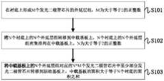
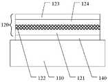
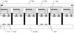
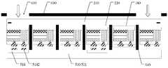
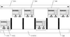
- A manufacturing method of a light-emitting diode substrate comprises the following steps:forming an epitaxial layer group of M light-emitting diode chips on the substrate;transferring N epitaxial layer groups on N substrates onto an intermediate substrate, wherein the N epitaxial layer groups on the N substrates are densely arranged on the intermediate substrate; andtransferring at least part of the light emitting diode chips in the N x M light emitting diode chips corresponding to the N epitaxial layer groups on the intermediate load substrate to a driving substrate,the area of the middle carrying base plate is larger than or equal to the sum of the areas of the N substrates, M is a positive integer larger than or equal to 2, and N is a positive integer larger than or equal to 2.
- The method of claim 1, wherein a distance between two adjacent epitaxial layer groups is substantially equal to a distance between two adjacent light emitting diode chips on the interposer substrate.
- The method of manufacturing a light-emitting diode substrate according to claim 1, wherein the shape of the interposer substrate is substantially the same as the shape of the driving substrate, and the area of the interposer substrate is substantially the same as the area of the driving substrate.
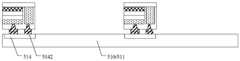
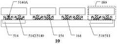
- The method of claim 1, wherein the driving substrate comprises a substrate base and a plurality of driving circuits disposed on the substrate base, each driving circuit comprises a pad and is configured to drive the light emitting diode chip electrically connected to the pad to emit light, the method further comprising:and binding the light emitting diode chip transferred onto the driving substrate with the corresponding gasket of the driving circuit by adopting a binding process.
- The method of manufacturing a light emitting diode substrate according to claim 4, wherein the bonding the light emitting diode chips transferred onto the driving substrate and the corresponding pads of the driving circuit using a bonding process comprises:and carrying out thermal reflow on the driving substrate so as to bond the light-emitting diode chip and the gasket together.
- The method of claim 4, wherein the driving substrate further comprises a plurality of conductive bumps on a side of the pads away from the substrate, and an orthogonal projection of each of the pads on the substrate overlaps an orthogonal projection of at least one of the conductive bumps on the substrate, the method further comprising:before at least part of the N x M light-emitting diode chips corresponding to the N epitaxial layer groups on the intermediate load substrate are transferred to the driving substrate, coating an organic insulating glue material on the driving substrate;the bonding the light emitting diode chip transferred onto the driving substrate and the corresponding pad of the driving circuit by using a bonding process includes:and carrying out thermal reflux on the driving substrate, and evaporating the solvent in the organic insulating glue material to bond the light-emitting diode chip and the gasket together.
- The method of claim 1, wherein transferring the N groups of epitaxial layers on the N substrates to the interposer substrate comprises:forming a first glue layer on the intermediate substrate; andand transferring N epitaxial layer groups on N substrates to one side of the first glue layer, which is far away from the intermediate load base plate.
- The method of claim 7, wherein the forming the first glue layer on the interposer substrate comprises:coating a first glue material layer on the middle loading substrate; andpatterning the first adhesive layer to form a plurality of through holes in the first adhesive layer through the first adhesive layer,the first adhesive layer including the plurality of through holes is the first adhesive layer, and the size of the orthographic projection of each through hole on the interposer substrate is smaller than the size of the orthographic projection of the light-emitting diode chip on the interposer substrate.
- The method for manufacturing the light-emitting diode substrate according to claim 7, wherein the material of the first adhesive layer comprises ultraviolet light-reduced adhesive or laser dissociation adhesive.
- The method of claim 7, wherein transferring N groups of the epitaxial layers on N of the substrates to the interposer substrate further comprises:before a first glue layer is formed on the intermediate substrate, a plurality of light shielding structures are formed on the intermediate substrate, and the orthographic projection of each light shielding structure on the intermediate substrate is positioned between the orthographic projections of two adjacent light emitting diode chips on the intermediate substrate.
- The method of fabricating a light-emitting diode submount of any of claims 1-10, wherein, after forming a group of epitaxial layers of M light-emitting diode chips on the substrate, the method of fabricating further comprises:forming M electrode structures on one side of the epitaxial layer group away from the substrate; andand dividing the epitaxial layer group and the M electrode structures to form M light-emitting diode chips.
- The method of claim 11, wherein the dividing the epitaxial layer group and the M electrode structures to form the M light emitting diode chips comprises:and dividing the epitaxial layer group and the M electrode structures by adopting an etching process to form M light-emitting diode chips.
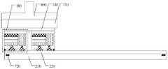
- The method of claim 11, wherein transferring N groups of the epitaxial layers on N of the substrates onto the interposer substrate comprises:transferring the substrate on which the M light emitting diode chips are formed onto a transfer substrate;peeling the substrate from the transfer substrate; andtransferring the N x M light emitting diode chips on the N transfer substrates to the intermediate substrate,wherein the area of the transfer substrate is substantially equal to the area of the substrate.
- The method of fabricating a light-emitting diode submount of claim 13, wherein transferring the substrate on which the M light-emitting diode chips are formed onto the transfer submount comprises:coating a second glue layer on the transfer substrate; andand transferring the substrate on which the M light-emitting diode chips are formed to the side, away from the transfer substrate, of the second glue layer.
- The method of claim 14, wherein the second adhesive layer is made of a material including uv-curable adhesive or laser-curable adhesive, and after transferring the N × M led chips on the N transfer substrates onto the interposer substrate, the transfer substrate is irradiated with light to reduce the viscosity of the second adhesive layer, so as to remove the transfer substrate.
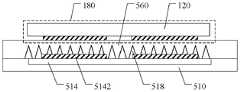
- The method of fabricating the light-emitting diode substrate as claimed in any one of claims 13 to 15, wherein the interposer substrate includes a plurality of first support structures, each of the first support structures has a dimension in a direction perpendicular to the interposer substrate that is greater than a dimension of the light-emitting diode chip in the direction perpendicular to the interposer substrate, and the transferring of the N by M light-emitting diode chips on the N transfer substrates onto the interposer substrate includes:and sequentially aligning the N transfer substrates with the intermediate load substrate, so that the plurality of first support structures are positioned between two adjacent light-emitting diode chips on the transfer substrates.
- The method for manufacturing the light-emitting diode substrate according to claim 16, wherein each of the first support structures is a columnar structure, and an orthographic projection shape of each of the first support structures on the interposer substrate includes one of a rectangle, a T-shape, and a circle.
- The method of claim 16, wherein each of the first supporting structures is a pillar-shaped structure, and orthographic projections of the first supporting structures on the interposer substrate are connected to form a grid.
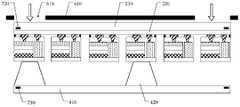
- The method of claim 16, wherein transferring at least some of the N x M led chips associated with the N epitaxial layer groups on the interposer substrate onto the driving substrate comprises:aligning the intermediate substrate with the driving substrate so that the first support structures are located between the intermediate substrate and the driving substrate;aligning a first mask plate with the middle loading substrate, wherein the first mask plate comprises a plurality of openings, and the plurality of openings correspond to the plurality of light emitting diode chips to be transferred; andand irradiating light rays to the intermediate load substrate through the first mask plate so as to transfer a plurality of to-be-transferred light emitting diode chips to the driving substrate.
- The method of claim 19, wherein the first mask comprises a light absorbing material, and the light absorbing material has a light absorption rate of greater than 60%.
- The method for manufacturing the light-emitting diode substrate according to claim 19, wherein the first mask comprises:a first transparent substrate; anda first light absorption pattern layer on the first transparent substrate and including the plurality of openings,the first light absorption pattern layer is made of the light absorption material, and the light absorption rate of the light absorption material is larger than 60%.
- The method of manufacturing a light emitting diode substrate according to claim 21, wherein the first mask further comprises:a first magnetic attraction structure positioned between the first transparent substrate and the first light absorption pattern layer,the orthographic projection of the first magnetic attraction structure on the first transparent substrate and the orthographic projection of the plurality of openings on the first transparent substrate are arranged at intervals.
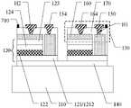
- The method of claim 19, wherein the driving substrate includes a plurality of first receiving structures, and aligning the interposer substrate with the driving substrate includes: inserting the plurality of first supporting structures on the intermediate load substrate into the plurality of first receiving structures on the driving substrate, wherein the plurality of first supporting structures and the plurality of first receiving structures are arranged in a one-to-one correspondence manner, and the size of each first receiving structure perpendicular to the driving substrate is smaller than the size of the light emitting diode chip perpendicular to the driving substrate.
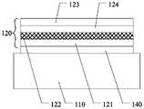
- The method of any one of claims 11-23, wherein forming the epitaxial layer group of M light emitting diode chips on the substrate comprises:forming a first conductive type semiconductor layer on the substrate;forming a light-emitting layer on one side of the first conductivity type semiconductor layer far away from the substrate; andand forming a second conductive type semiconductor layer on one side of the light emitting layer far away from the first conductive type semiconductor layer.
- The method of claim 24, wherein forming M of the electrode structures on a side of the epitaxial layer group away from the substrate comprises:patterning the epitaxial group layer to expose a portion of the first conductive type semiconductor layer to form M exposed portions;forming M first electrodes on the sides of the M exposed parts far away from the substrate;forming M second electrodes on one side of the second conductivity type semiconductor layer far away from the substrate;forming a passivation layer on one side, far away from the substrate, of the M first electrodes and the M second electrodes;patterning the passivation layer to form a first via corresponding to the first electrode and a second via corresponding to the second electrode in the passivation layer;forming a first electrode pad and a second electrode pad on one side of the passivation layer away from the substrate, wherein the first electrode pad is connected with the first electrode through the first via hole, and the second electrode pad is connected with the second electrode through the second via hole,wherein each of the conductive structures includes a first electrode, a first electrode pad, a second electrode, and a second electrode pad.
- The method of claim 25, wherein forming the epitaxial layer group of M light emitting diode chips on the substrate further comprises:an electron blocking layer is formed between the light emitting layer and the second conductive type semiconductor layer.
- The method of manufacturing a light-emitting diode substrate according to claim 25, wherein before the first conductivity-type semiconductor layer is formed on the substrate, the method further comprises:carrying out high-temperature treatment on the substrate, and cleaning the surface of the substrate; anda buffer layer is formed on the substrate.
- The method for manufacturing a light-emitting diode substrate according to claim 25, wherein the first conductivity type semiconductor layer is an n-type semiconductor layer, and the second conductivity type semiconductor layer is a p-type semiconductor layer.
- The method of manufacturing a light-emitting diode substrate according to claim 27, wherein the first conductivity type semiconductor layer is n-type gallium nitride, the second conductivity type semiconductor layer is p-type gallium nitride, and the buffer layer is aluminum nitride.
- The method of claim 11, wherein transferring at least some of the N x M led chips associated with the N epitaxial layer groups on the interposer substrate onto the driving substrate comprises:providing a selection substrate, wherein the selection substrate comprises a plurality of selection structures;aligning the selection substrate with the intermediate load substrate, and contacting the plurality of selection structures with the plurality of light emitting diode chips to be transferred;aligning a second mask plate with the intermediate-load substrate, wherein the second mask plate comprises a plurality of openings, and the plurality of openings correspond to the plurality of selecting structures;irradiating light rays to the intermediate load substrate through the second mask plate so as to transfer a plurality of light emitting diode chips to be transferred to a plurality of selecting structures on the selecting substrate;aligning the selected substrate with the driving substrate;bonding the plurality of light emitting diode chips to be transferred on the plurality of selection structures on the selection substrate with the driving substrate; andremoving a plurality of the selection structures.
- The method of claim 30, wherein the second mask comprises a light absorbing material, and the light absorbing material has a light absorption rate of greater than 60%.
- The method for manufacturing the light-emitting diode substrate according to claim 31, wherein the second mask comprises:a second transparent substrate; anda second light absorption pattern layer on the second transparent substrate and including the plurality of openings,the second light absorption pattern layer is made of the light absorption material, and the light absorption rate of the light absorption material is larger than 60%.
- The method of claim 32, wherein the second mask further comprises:a second magnetic structure between the second transparent substrate and the second light absorption pattern layer,the orthographic projection of the second magnetic attraction structure on the second transparent substrate and the orthographic projection of the plurality of openings on the second transparent substrate are arranged at intervals.
- The method of claim 30, wherein each of the selected structures comprises a support portion and a pyrolytic portion located on the support portion away from the interposer substrate.
- The method of claim 34, wherein aligning the pick substrate with the interposer substrate, the contacting the pick structures with the plurality of led chips to be transferred comprises:aligning the selected substrate with the intermediate carrying substrate in a vacuum environment;and applying pressure to the selection substrate to enable the pyrolysis part in the selection structure to be adhered to the corresponding light emitting diode chip.
- The method of claim 35, wherein the step of irradiating the intermediate substrate with light through the second mask to transfer the plurality of led chips to be transferred to the plurality of selected structures on the selected substrate comprises:and after the second mask plate irradiates light to the intermediate load substrate, introducing inert gas between the selected substrate and the intermediate load substrate.
- The method of claim 34, wherein removing the plurality of selected structures comprises:heating in a vacuum environment to melt the pyrolysis section to remove the plurality of selected structures.
- The method of claim 30, wherein the material of each of the selected structures includes an ultraviolet reduced glue or a laser dissociated glue, and removing the plurality of selected structures includes:and irradiating light rays to the selected substrate to remove the plurality of selected structures.
- The method of claim 30, wherein each of the selected structures comprises an elastomeric material.
- The method of claim 30, wherein a cross-section of each of the selected structures taken perpendicular to a plane of the selected substrate has a shape that includes a trapezoid.
- The method of fabricating a light-emitting diode substrate as claimed in any one of claims 13 to 15, wherein the driving substrate includes a plurality of second support structures, each of which has a dimension in a direction perpendicular to the driving substrate larger than a dimension of the light-emitting diode chip in the direction perpendicular to the driving substrate.
- The method of claim 41, wherein transferring at least some of the N by M of the LED chips associated with the N epitaxial layers on the interposer substrate to the driving substrate comprises:aligning the intermediate substrate with the driving substrate, and inserting the second support structures between two adjacent light emitting diode chips on the intermediate substrate;aligning a third mask plate with the middle loading substrate, wherein the third mask plate comprises a plurality of openings, and the plurality of openings correspond to the plurality of light emitting diode chips to be transferred; andand irradiating light rays to the intermediate load substrate through the third mask plate so as to transfer a plurality of light-emitting diode chips to be transferred to the driving substrate.
- The method of any one of claims 1-10, wherein transferring N groups of the epitaxial layers on N of the substrates onto the interposer substrate comprises:sequentially transferring N epitaxial layer groups on N substrates to the intermediate load base plate;forming M electrode structures on one sides of the N epitaxial layer groups, which are far away from the intermediate load substrate;and dividing the N epitaxial layer groups on the intermediate substrate to form M light-emitting diode chips together with the M electrode structures.
- The method of claim 43, wherein the dividing the N epitaxial layers on the interposer substrate to form M LED chips together with the M electrode structure groups comprises:and dividing the N epitaxial layer groups on the mid-load substrate by adopting an etching process so as to form M light-emitting diode chips together with the M electrode structure groups.
- The method of claim 44, wherein forming the epitaxial layer group of M light-emitting diode chips on the substrate comprises:forming a first conductive type semiconductor layer on the substrate;forming a light-emitting layer on one side of the first conductivity type semiconductor layer far away from the substrate; andand forming a second conductive type semiconductor layer on one side of the light emitting layer far away from the first conductive type semiconductor layer.
- The method of manufacturing a light-emitting diode substrate according to claim 45, wherein before the first conductivity-type semiconductor layer is formed on the substrate, the method further comprises:carrying out high-temperature treatment on the substrate, and cleaning the surface of the substrate; anda buffer layer is formed on the substrate.
- The method for manufacturing a light-emitting diode substrate according to claim 45, wherein the first conductivity type semiconductor layer is an n-type semiconductor layer, and the second conductivity type semiconductor layer is a p-type semiconductor layer.
- The method of manufacturing a light-emitting diode substrate according to claim 46, wherein the first conductivity type semiconductor layer is n-type gallium nitride, the second conductivity type semiconductor layer is p-type gallium nitride, and the buffer layer is aluminum nitride.
- The method of claim 45, wherein each of the electrode structures includes a first electrode and J second electrodes, and wherein forming M of the electrode structures on the side of the epitaxial layer group away from the substrate comprises:patterning the epitaxial group layer to expose a portion of the first conductive type semiconductor layer to form M exposed portions, and dividing the second conductive type semiconductor layer into M × J second conductive type semiconductor tiles;forming M second electrodes on the side, away from the intermediate carrier substrate, of the M second conductive type semiconductor blocks;forming a passivation layer on one side of the M X J second electrodes far away from the intermediate load substrate;patterning the passivation layer to form M first vias corresponding to the M exposed portions and M × J second vias corresponding to the M × J second electrodes in the passivation layer;forming M first electrodes on one sides of the M exposed parts far away from the substrate through M first through holes; andforming a first electrode pad and a second electrode pad on one side of the passivation layer far away from the intermediate load substrate, wherein the first electrode pad is connected with the first electrode through the first via hole, the second electrode pad is connected with the second electrode through the second via hole,wherein J is a positive integer of 2 or more.
- The method of claim 46, wherein forming the epitaxial layer group of M light-emitting diode chips on the substrate further comprises:an electron blocking layer is formed between the light emitting layer and the second conductive type semiconductor layer.
- The method of fabricating the light-emitting diode submount of any of claims 1-10, wherein forming the group of epitaxial layers of the M light-emitting diode chips on the substrate comprises:forming the epitaxial layer groups of the M light-emitting diode chips on the circular substrate; andcutting the substrate in a circular shape into the substrate in a square shape or a hexagonal shape along the edge of the epitaxial layer group,wherein the shape of the orthographic projection of the epitaxial layer group on the substrate is square.
- The method of claim 51, wherein transferring N groups of the epitaxial layers on N of the substrates onto the interposer substrate comprises:and densely arranging N epitaxial layer groups on N square or hexagonal substrates on the intermediate load base plate.
- The method of fabricating the light-emitting diode submount of any of claims 1-10, wherein forming the group of epitaxial layers of the M light-emitting diode chips on the substrate comprises:cutting the substrate in a circular shape into the substrate in a square shape or a hexagonal shape;stitching together N square or hexagonal said substrates to form a combination of N said substrates;forming said epitaxial layers of M x N said light emitting diode chips on a combination of N said substrates.
- The method of claim 53, wherein transferring N groups of the epitaxial layers on N of the substrates onto the interposer substrate comprises:the epitaxial layers of M x N of the LED chips formed on the combination of N of the substrates are transferred onto the interposer substrate.
- The method of claim 4, wherein each of the pads comprises at least two sub-pads, each of the sub-pads comprising a recess configured to receive an electrode pad of a corresponding one of the LED chips.
- A light emitting diode substrate manufactured by the manufacturing method according to any one of claims 1 to 3.
- The light-emitting diode submount of claim 56, wherein the drive submount comprises a plurality of receiving structures, each of the first receiving structures having a dimension perpendicular to the drive submount that is smaller than a dimension of the light-emitting diode chip perpendicular to the drive submount.
- The light emitting diode substrate of claim 56, further comprising:and the size of each supporting structure in the direction perpendicular to the driving substrate is larger than that of each light-emitting diode chip in the direction perpendicular to the driving substrate.
- The light-emitting diode submount of claim 56, wherein the drive submount comprises a substrate submount and a plurality of drive circuits on the substrate submount, each of the drive circuits comprising a pad and being configured to drive the light-emitting diode chips electrically connected to the pad to emit light, each of the pads comprising at least two sub-pads, each of the sub-pads comprising a recess configured to receive an electrode pad of a corresponding one of the light-emitting diode chips.
- A display device comprising the light emitting diode substrate of any one of claims 56-59.
Applications Claiming Priority (1)
| Application Number | Priority Date | Filing Date | Title |
|---|---|---|---|
| PCT/CN2020/125490WO2022088093A1 (en) | 2020-10-30 | 2020-10-30 | Light emitting diode substrate and manufacturing method therefor, and display apparatus |
Publications (2)
| Publication Number | Publication Date |
|---|---|
| CN114698401Atrue CN114698401A (en) | 2022-07-01 |
| CN114698401B CN114698401B (en) | 2025-03-21 |
Family
ID=81381598
Family Applications (1)
| Application Number | Title | Priority Date | Filing Date |
|---|---|---|---|
| CN202080002595.8AActiveCN114698401B (en) | 2020-10-30 | 2020-10-30 | Light-emitting diode substrate and manufacturing method thereof, and display device |
Country Status (5)
| Country | Link |
|---|---|
| US (2) | US12249529B2 (en) |
| EP (1) | EP4174963A4 (en) |
| CN (1) | CN114698401B (en) |
| TW (2) | TWI813030B (en) |
| WO (1) | WO2022088093A1 (en) |
Families Citing this family (14)
| Publication number | Priority date | Publication date | Assignee | Title |
|---|---|---|---|---|
| KR20230099234A (en)* | 2021-12-27 | 2023-07-04 | 삼성전자주식회사 | printed circuit board and Semiconductor package comprising the same |
| CN115810702A (en)* | 2022-04-01 | 2023-03-17 | 友达光电股份有限公司 | Light-emitting element panel |
| CN117317073A (en)* | 2022-06-23 | 2023-12-29 | 成都辰显光电有限公司 | Transfer device and preparation method thereof |
| CN115241113A (en)* | 2022-06-24 | 2022-10-25 | 佛山市国星光电股份有限公司 | A chip transfer device |
| CN115255678B (en)* | 2022-09-22 | 2022-12-09 | 苏州芯海半导体科技有限公司 | Semiconductor wafer double-film cutting equipment |
| CN115312637B (en)* | 2022-10-11 | 2022-12-16 | 罗化芯显示科技开发(江苏)有限公司 | A kind of Micro-LED display device and its manufacturing method |
| CN115903306B (en)* | 2022-11-14 | 2024-12-06 | 上海芯元基半导体科技有限公司 | A method for preparing a backlight module, a chip module, and a backlight module |
| WO2024124540A1 (en) | 2022-12-16 | 2024-06-20 | 厦门市芯颖显示科技有限公司 | Transfer carrier plate, transfer assembly, and micro-device transfer method |
| CN118511267A (en) | 2022-12-16 | 2024-08-16 | 厦门市芯颖显示科技有限公司 | Transfer plate, transfer assembly and micro device transfer method |
| KR20240105655A (en)* | 2022-12-28 | 2024-07-08 | 엘지디스플레이 주식회사 | Display apparatus and manufacturing method of display apparatus |
| WO2024197607A1 (en)* | 2023-03-28 | 2024-10-03 | 京东方科技集团股份有限公司 | Display substrate, display panel and manufacturing method |
| CN116154057B (en)* | 2023-03-30 | 2024-08-02 | 惠科股份有限公司 | Transfer method, display panel and transient substrate |
| CN118073483B (en)* | 2024-01-19 | 2024-11-29 | 惠科股份有限公司 | Transfer method, transfer module and display panel |
| CN119108482B (en)* | 2024-08-30 | 2025-05-13 | 惠科股份有限公司 | Display panel, display device, and method for manufacturing display panel |
Citations (4)
| Publication number | Priority date | Publication date | Assignee | Title |
|---|---|---|---|---|
| US20100259164A1 (en)* | 2009-04-10 | 2010-10-14 | Sony Corporation | Manufacturing method of display device and display device |
| US20190043843A1 (en)* | 2017-08-01 | 2019-02-07 | Innolux Corporation | Methods for manufacturing a display device |
| US20190044023A1 (en)* | 2017-08-01 | 2019-02-07 | Innolux Corporation | Methods for manufacturing semiconductor device |
| US20190393069A1 (en)* | 2018-06-22 | 2019-12-26 | Veeco Instruments Inc. | Micro-LED Transfer Methods Using Light-Based Debonding |
Family Cites Families (24)
| Publication number | Priority date | Publication date | Assignee | Title |
|---|---|---|---|---|
| TWI557831B (en) | 2015-05-15 | 2016-11-11 | 友達光電股份有限公司 | Micro component transfer method |
| KR20180022683A (en) | 2015-07-23 | 2018-03-06 | 서울반도체 주식회사 | Display device and manufacturing method thereof |
| US9640108B2 (en)* | 2015-08-25 | 2017-05-02 | X-Celeprint Limited | Bit-plane pulse width modulated digital display system |
| WO2017037475A1 (en) | 2015-09-02 | 2017-03-09 | Oculus Vr, Llc | Assembly of semiconductor devices |
| US10068888B2 (en) | 2015-12-21 | 2018-09-04 | Hong Kong Beida Jade Bird Display Limited | Making semiconductor devices with alignment bonding and substrate removal |
| WO2018087704A2 (en) | 2016-11-11 | 2018-05-17 | QMAT, Inc. | Micro-light emitting diode (led) fabrication by layer transfer |
| TWI756384B (en) | 2017-03-16 | 2022-03-01 | 美商康寧公司 | Method and process for mass transfer of micro-leds |
| CN107017319A (en) | 2017-05-23 | 2017-08-04 | 深圳市华星光电技术有限公司 | The preparation method of colored micro- LED array substrate |
| KR102514755B1 (en) | 2017-07-10 | 2023-03-29 | 삼성전자주식회사 | Micro led display and mamufacturing method thereof |
| TW201911457A (en) | 2017-07-26 | 2019-03-16 | 優顯科技股份有限公司 | Method for batch shifting micro-semiconductor structures |
| CN107946415B (en) | 2017-11-15 | 2019-06-25 | 上海天马微电子有限公司 | Display panel and manufacturing method thereof |
| US10989376B2 (en) | 2017-11-28 | 2021-04-27 | Facebook Technologies, Llc | Assembling of strip of micro light emitting diodes onto backplane |
| CN108538878A (en) | 2018-07-11 | 2018-09-14 | 大连德豪光电科技有限公司 | Micro- light emitting diode base plate and preparation method thereof, display device |
| CN110021237B (en) | 2018-09-17 | 2020-11-24 | 东莞市中晶半导体科技有限公司 | A method of transferring MICRO LED chips from wafer to panel |
| CN109473532B (en) | 2018-11-20 | 2020-11-06 | 合肥京东方光电科技有限公司 | Manufacturing method of Micro LED display substrate |
| CN111244008A (en) | 2018-11-29 | 2020-06-05 | 昆山工研院新型平板显示技术中心有限公司 | Micro-component transfer device and transfer method thereof |
| CN111033737B (en)* | 2019-03-25 | 2024-02-06 | 湖北三安光电有限公司 | Microluminescent component, microluminescent diode and microluminescent diode transfer method |
| CN110010729A (en)* | 2019-03-28 | 2019-07-12 | 王晓靁 | RGB full-color InGaN-based LED and preparation method thereof |
| CN112018143A (en) | 2019-05-28 | 2020-12-01 | 云谷(固安)科技有限公司 | Micro light-emitting diode display substrate, display panel, manufacturing method thereof, and display device |
| CN110690243B (en) | 2019-10-15 | 2022-06-17 | 京东方科技集团股份有限公司 | A display panel and a method for producing the same |
| CN111244004A (en) | 2020-01-19 | 2020-06-05 | 南京中电熊猫平板显示科技有限公司 | Transfer method and transfer substrate of micro light-emitting diode |
| CN111128813B (en) | 2020-01-20 | 2022-10-28 | 福州大学 | Mu LED mass transfer method |
| CN111261658B (en) | 2020-02-10 | 2023-02-28 | Tcl华星光电技术有限公司 | Micro light-emitting diode display panel and transfer printing method of micro light-emitting diode |
| CN111564393B (en)* | 2020-05-21 | 2022-10-18 | 厦门乾照半导体科技有限公司 | A kind of transfer method of LED chip |
- 2020
- 2020-10-30EPEP20959255.9Apatent/EP4174963A4/enactivePending
- 2020-10-30USUS17/427,628patent/US12249529B2/enactiveActive
- 2020-10-30CNCN202080002595.8Apatent/CN114698401B/enactiveActive
- 2020-10-30WOPCT/CN2020/125490patent/WO2022088093A1/ennot_activeCeased
- 2021
- 2021-09-30TWTW110136419Apatent/TWI813030B/enactive
- 2021-09-30TWTW112127532Apatent/TW202411975A/enunknown
- 2025
- 2025-02-03USUS19/043,901patent/US20250183089A1/enactivePending
Patent Citations (4)
| Publication number | Priority date | Publication date | Assignee | Title |
|---|---|---|---|---|
| US20100259164A1 (en)* | 2009-04-10 | 2010-10-14 | Sony Corporation | Manufacturing method of display device and display device |
| US20190043843A1 (en)* | 2017-08-01 | 2019-02-07 | Innolux Corporation | Methods for manufacturing a display device |
| US20190044023A1 (en)* | 2017-08-01 | 2019-02-07 | Innolux Corporation | Methods for manufacturing semiconductor device |
| US20190393069A1 (en)* | 2018-06-22 | 2019-12-26 | Veeco Instruments Inc. | Micro-LED Transfer Methods Using Light-Based Debonding |
Also Published As
| Publication number | Publication date |
|---|---|
| US12249529B2 (en) | 2025-03-11 |
| US20250183089A1 (en) | 2025-06-05 |
| TW202217783A (en) | 2022-05-01 |
| US20220352000A1 (en) | 2022-11-03 |
| TWI813030B (en) | 2023-08-21 |
| WO2022088093A1 (en) | 2022-05-05 |
| EP4174963A1 (en) | 2023-05-03 |
| TW202411975A (en) | 2024-03-16 |
| CN114698401B (en) | 2025-03-21 |
| EP4174963A4 (en) | 2023-08-23 |
Similar Documents
| Publication | Publication Date | Title |
|---|---|---|
| CN114698401A (en) | Light emitting diode substrate, manufacturing method thereof and display device | |
| TWI745206B (en) | Light emitting unit and display apparatus | |
| KR102514503B1 (en) | Display device manufacturing method | |
| TWI630731B (en) | White light emitting diode component | |
| US20120142124A1 (en) | Method of applying phosphor to semiconductor light-emitting device | |
| US20130114255A1 (en) | Broad-area lighting systems | |
| US20210135042A1 (en) | Method for transferring micro light-emitting diodes and transferring device | |
| CN1947222A (en) | Flip Chip Light Emitting Diode Device Without Submount | |
| CN110034224A (en) | A kind of transfer method based on bar shaped Micro-LED | |
| JP2020068313A (en) | Light emitting element and manufacturing method of display device | |
| CN115000278A (en) | Light emitting device package with reflective side cladding layer | |
| JP7212061B2 (en) | LED backplane with flat bonding surface and manufacturing method thereof | |
| WO2012118303A9 (en) | Light-emitting diode chip | |
| WO2019109888A1 (en) | Method for cutting semiconductor package module and semiconductor package unit | |
| TWI467808B (en) | Light-emitting diode element, manufacturing method thereof and light-emitting device | |
| CN113471339B (en) | Mass transfer method of Micro-LED chips | |
| KR20180023881A (en) | Sheet lighting and manufacturing method of the same | |
| JP4631232B2 (en) | Circuit element bonding method and electric circuit device manufacturing method | |
| TWI777435B (en) | Micro led carrier board | |
| CN111628053B (en) | Miniature LED carrier plate | |
| CN105164825B (en) | Method for manufacturing opto-electronic device | |
| TWI830256B (en) | Transfer method of led chip | |
| JP2021072390A (en) | Method for manufacturing light emitting device | |
| KR100857763B1 (en) | Board Bonding Device | |
| KR20180014473A (en) | Sheet lighting and manufacturing method of the same |
Legal Events
| Date | Code | Title | Description |
|---|---|---|---|
| PB01 | Publication | ||
| PB01 | Publication | ||
| SE01 | Entry into force of request for substantive examination | ||
| SE01 | Entry into force of request for substantive examination | ||
| GR01 | Patent grant | ||
| GR01 | Patent grant |