CN114695559A - Thin film transistor, method of manufacturing thin film transistor, and display device including thin film transistor - Google Patents
Thin film transistor, method of manufacturing thin film transistor, and display device including thin film transistorDownload PDFInfo
- Publication number
- CN114695559A CN114695559ACN202111622115.0ACN202111622115ACN114695559ACN 114695559 ACN114695559 ACN 114695559ACN 202111622115 ACN202111622115 ACN 202111622115ACN 114695559 ACN114695559 ACN 114695559A
- Authority
- CN
- China
- Prior art keywords
- gate electrode
- active layer
- thin film
- film transistor
- layer
- Prior art date
- Legal status (The legal status is an assumption and is not a legal conclusion. Google has not performed a legal analysis and makes no representation as to the accuracy of the status listed.)
- Pending
Links
Images


Classifications
- H—ELECTRICITY
- H01—ELECTRIC ELEMENTS
- H01L—SEMICONDUCTOR DEVICES NOT COVERED BY CLASS H10
- H01L21/00—Processes or apparatus adapted for the manufacture or treatment of semiconductor or solid state devices or of parts thereof
- H01L21/02—Manufacture or treatment of semiconductor devices or of parts thereof
- H01L21/04—Manufacture or treatment of semiconductor devices or of parts thereof the devices having potential barriers, e.g. a PN junction, depletion layer or carrier concentration layer
- H01L21/34—Manufacture or treatment of semiconductor devices or of parts thereof the devices having potential barriers, e.g. a PN junction, depletion layer or carrier concentration layer the devices having semiconductor bodies not provided for in groups H01L21/18, H10D48/04 and H10D48/07, with or without impurities, e.g. doping materials
- H—ELECTRICITY
- H10—SEMICONDUCTOR DEVICES; ELECTRIC SOLID-STATE DEVICES NOT OTHERWISE PROVIDED FOR
- H10D—INORGANIC ELECTRIC SEMICONDUCTOR DEVICES
- H10D30/00—Field-effect transistors [FET]
- H10D30/60—Insulated-gate field-effect transistors [IGFET]
- H10D30/67—Thin-film transistors [TFT]
- H10D30/6729—Thin-film transistors [TFT] characterised by the electrodes
- H10D30/673—Thin-film transistors [TFT] characterised by the electrodes characterised by the shapes, relative sizes or dispositions of the gate electrodes
- H10D30/6733—Multi-gate TFTs
- H10D30/6734—Multi-gate TFTs having gate electrodes arranged on both top and bottom sides of the channel, e.g. dual-gate TFTs
- H—ELECTRICITY
- H10—SEMICONDUCTOR DEVICES; ELECTRIC SOLID-STATE DEVICES NOT OTHERWISE PROVIDED FOR
- H10D—INORGANIC ELECTRIC SEMICONDUCTOR DEVICES
- H10D30/00—Field-effect transistors [FET]
- H10D30/60—Insulated-gate field-effect transistors [IGFET]
- H10D30/67—Thin-film transistors [TFT]
- H10D30/674—Thin-film transistors [TFT] characterised by the active materials
- H10D30/6755—Oxide semiconductors, e.g. zinc oxide, copper aluminium oxide or cadmium stannate
- H—ELECTRICITY
- H10—SEMICONDUCTOR DEVICES; ELECTRIC SOLID-STATE DEVICES NOT OTHERWISE PROVIDED FOR
- H10D—INORGANIC ELECTRIC SEMICONDUCTOR DEVICES
- H10D30/00—Field-effect transistors [FET]
- H10D30/60—Insulated-gate field-effect transistors [IGFET]
- H10D30/67—Thin-film transistors [TFT]
- H10D30/6757—Thin-film transistors [TFT] characterised by the structure of the channel, e.g. transverse or longitudinal shape or doping profile
- H—ELECTRICITY
- H10—SEMICONDUCTOR DEVICES; ELECTRIC SOLID-STATE DEVICES NOT OTHERWISE PROVIDED FOR
- H10D—INORGANIC ELECTRIC SEMICONDUCTOR DEVICES
- H10D86/00—Integrated devices formed in or on insulating or conducting substrates, e.g. formed in silicon-on-insulator [SOI] substrates or on stainless steel or glass substrates
- H10D86/40—Integrated devices formed in or on insulating or conducting substrates, e.g. formed in silicon-on-insulator [SOI] substrates or on stainless steel or glass substrates characterised by multiple TFTs
- H10D86/421—Integrated devices formed in or on insulating or conducting substrates, e.g. formed in silicon-on-insulator [SOI] substrates or on stainless steel or glass substrates characterised by multiple TFTs having a particular composition, shape or crystalline structure of the active layer
- H10D86/423—Integrated devices formed in or on insulating or conducting substrates, e.g. formed in silicon-on-insulator [SOI] substrates or on stainless steel or glass substrates characterised by multiple TFTs having a particular composition, shape or crystalline structure of the active layer comprising semiconductor materials not belonging to the Group IV, e.g. InGaZnO
- H—ELECTRICITY
- H10—SEMICONDUCTOR DEVICES; ELECTRIC SOLID-STATE DEVICES NOT OTHERWISE PROVIDED FOR
- H10D—INORGANIC ELECTRIC SEMICONDUCTOR DEVICES
- H10D86/00—Integrated devices formed in or on insulating or conducting substrates, e.g. formed in silicon-on-insulator [SOI] substrates or on stainless steel or glass substrates
- H10D86/40—Integrated devices formed in or on insulating or conducting substrates, e.g. formed in silicon-on-insulator [SOI] substrates or on stainless steel or glass substrates characterised by multiple TFTs
- H10D86/421—Integrated devices formed in or on insulating or conducting substrates, e.g. formed in silicon-on-insulator [SOI] substrates or on stainless steel or glass substrates characterised by multiple TFTs having a particular composition, shape or crystalline structure of the active layer
- H10D86/425—Integrated devices formed in or on insulating or conducting substrates, e.g. formed in silicon-on-insulator [SOI] substrates or on stainless steel or glass substrates characterised by multiple TFTs having a particular composition, shape or crystalline structure of the active layer having different crystal properties in different TFTs or within an individual TFT
- H—ELECTRICITY
- H10—SEMICONDUCTOR DEVICES; ELECTRIC SOLID-STATE DEVICES NOT OTHERWISE PROVIDED FOR
- H10D—INORGANIC ELECTRIC SEMICONDUCTOR DEVICES
- H10D86/00—Integrated devices formed in or on insulating or conducting substrates, e.g. formed in silicon-on-insulator [SOI] substrates or on stainless steel or glass substrates
- H10D86/40—Integrated devices formed in or on insulating or conducting substrates, e.g. formed in silicon-on-insulator [SOI] substrates or on stainless steel or glass substrates characterised by multiple TFTs
- H10D86/60—Integrated devices formed in or on insulating or conducting substrates, e.g. formed in silicon-on-insulator [SOI] substrates or on stainless steel or glass substrates characterised by multiple TFTs wherein the TFTs are in active matrices
- H—ELECTRICITY
- H10—SEMICONDUCTOR DEVICES; ELECTRIC SOLID-STATE DEVICES NOT OTHERWISE PROVIDED FOR
- H10D—INORGANIC ELECTRIC SEMICONDUCTOR DEVICES
- H10D99/00—Subject matter not provided for in other groups of this subclass
- H—ELECTRICITY
- H10—SEMICONDUCTOR DEVICES; ELECTRIC SOLID-STATE DEVICES NOT OTHERWISE PROVIDED FOR
- H10D—INORGANIC ELECTRIC SEMICONDUCTOR DEVICES
- H10D30/00—Field-effect transistors [FET]
- H10D30/60—Insulated-gate field-effect transistors [IGFET]
- H10D30/67—Thin-film transistors [TFT]
- H10D30/6729—Thin-film transistors [TFT] characterised by the electrodes
- H10D30/6737—Thin-film transistors [TFT] characterised by the electrodes characterised by the electrode materials
- H10D30/6739—Conductor-insulator-semiconductor electrodes
Landscapes
- Engineering & Computer Science (AREA)
- Physics & Mathematics (AREA)
- Condensed Matter Physics & Semiconductors (AREA)
- General Physics & Mathematics (AREA)
- Manufacturing & Machinery (AREA)
- Computer Hardware Design (AREA)
- Microelectronics & Electronic Packaging (AREA)
- Power Engineering (AREA)
- Thin Film Transistor (AREA)
Abstract
Description
Translated fromChinese相关申请的交叉引用CROSS-REFERENCE TO RELATED APPLICATIONS
本申请要求2020年12月29日提交的韩国专利申请No.10-2020-0186700和2021年12月9日提交的韩国专利申请No.10-2021-0175278的权益,上述专利申请通过引用在此被并入,如同其完整地在本文中被阐述一样。This application claims the benefit of Korean Patent Application No. 10-2020-0186700 filed on December 29, 2020 and Korean Patent Application No. 10-2021-0175278 filed on December 9, 2021, which are incorporated herein by reference is incorporated as if fully set forth herein.
技术领域technical field
本公开涉及薄膜晶体管、制造薄膜晶体管的方法和包括薄膜晶体管的显示装置。The present disclosure relates to thin film transistors, methods of manufacturing the thin film transistors, and display devices including the thin film transistors.
背景技术Background technique
由于可以在玻璃基板或塑料基板上制造薄膜晶体管,薄膜晶体管已被广泛地用作诸如液晶显示装置或有机发光装置的显示装置的开关元件或驱动元件。Since thin film transistors can be fabricated on glass substrates or plastic substrates, thin film transistors have been widely used as switching elements or driving elements of display devices such as liquid crystal display devices or organic light emitting devices.
薄膜晶体管可基于构成有源层的材料被分类为其中非晶硅被用作有源层的非晶硅薄膜晶体管、其中多晶硅被用作有源层的多晶硅薄膜晶体管,以及其中氧化物半导体被用作有源层的氧化物半导体薄膜晶体管。Thin film transistors can be classified into amorphous silicon thin film transistors in which amorphous silicon is used as the active layer, polycrystalline silicon thin film transistors in which polycrystalline silicon is used as the active layer, and polycrystalline silicon thin film transistors in which oxide semiconductors are used based on the material constituting the active layer. An oxide semiconductor thin film transistor as the active layer.
由于非晶硅可以在短时间内沉积以形成有源层,非晶硅薄膜晶体管(a-Si TFT)具有制造过程时间短且生产成本低的优点。另一方面,非晶硅薄膜晶体管的缺点在于,其被限制用于有源矩阵有机发光二极管(AMOLED),因为由于低迁移率而导致电流驱动能力不佳且存在阈值电压的变化。Since amorphous silicon can be deposited in a short time to form an active layer, an amorphous silicon thin film transistor (a-Si TFT) has the advantages of short manufacturing process time and low production cost. On the other hand, amorphous silicon thin film transistors have the disadvantage that they are limited to active matrix organic light emitting diodes (AMOLEDs) due to poor current drive capability and threshold voltage variations due to low mobility.
多晶硅薄膜晶体管(poly-Si TFT)通过沉积非晶硅并使沉积的非晶硅晶化而制成。多晶硅薄膜晶体管的优点在于,电子迁移率高、稳定性优异、可实现薄型化和高分辨率以及功率效率(功效)高。多晶硅薄膜晶体管的一个示例为低温多晶硅(LTPS)薄膜晶体管。然而,由于制造多晶硅薄膜晶体管的过程需要使非晶硅晶化的步骤,归因于过程步骤的数量增加并且需要在高温下晶化,制造成本增加。因此,难以将多晶硅薄膜晶体管应用于大型(大尺寸)显示装置。此外,由于多晶特性,难以确保多晶硅薄膜晶体管的均匀性。Polycrystalline silicon thin film transistors (poly-Si TFTs) are fabricated by depositing amorphous silicon and crystallizing the deposited amorphous silicon. The advantages of polycrystalline silicon thin film transistors are high electron mobility, excellent stability, thinning and high resolution, and high power efficiency (efficiency). An example of a polysilicon thin film transistor is a low temperature polysilicon (LTPS) thin film transistor. However, since the process of manufacturing a polycrystalline silicon thin film transistor requires a step of crystallizing amorphous silicon, the manufacturing cost increases due to an increase in the number of process steps and the need to crystallize at a high temperature. Therefore, it is difficult to apply polysilicon thin film transistors to large-scale (large-size) display devices. In addition, due to polycrystalline characteristics, it is difficult to ensure uniformity of polycrystalline silicon thin film transistors.
具有高迁移率且根据氧含量具有大的电阻变化的氧化物半导体薄膜晶体管(TFT)具有可易于获得期望的特性的优点。此外,由于在制造氧化物半导体薄膜晶体管的过程期间构成有源层的氧化物可在相对低的温度下生长,氧化物半导体薄膜晶体管的制造成本降低。考虑到氧化物的特性,由于氧化物半导体是透明的,因此有利于实现透明显示器。然而,与多晶硅薄膜晶体管相比,氧化物半导体薄膜晶体管具有稳定性和电子迁移率劣化的问题。An oxide semiconductor thin film transistor (TFT) having high mobility and large resistance change according to oxygen content has an advantage that desired characteristics can be easily obtained. In addition, since the oxide constituting the active layer can be grown at a relatively low temperature during the process of manufacturing the oxide semiconductor thin film transistor, the manufacturing cost of the oxide semiconductor thin film transistor is reduced. Considering the properties of oxides, since oxide semiconductors are transparent, it is advantageous to realize a transparent display. However, oxide semiconductor thin film transistors have problems of deterioration in stability and electron mobility compared to polysilicon thin film transistors.
当氧化物半导体薄膜晶体管(TFT)长时间在接通(ON)状态下被驱动时,阈值电压趋向于持续地变化。由于TFT的驱动特征的这种变化,装置的寿命可能缩短,图像质量可能降低,且可能需要昂贵的补偿技术和附加电路。因此,需要改善氧化物半导体薄膜晶体管的驱动稳定性。When an oxide semiconductor thin film transistor (TFT) is driven in an ON state for a long time, the threshold voltage tends to change continuously. Due to such changes in the driving characteristics of the TFTs, the lifetime of the device may be shortened, the image quality may be degraded, and expensive compensation techniques and additional circuitry may be required. Therefore, there is a need to improve the driving stability of oxide semiconductor thin film transistors.
发明内容SUMMARY OF THE INVENTION
考虑到上述问题给出了本公开,并且本公开的目的在于提供一种薄膜晶体管,其具有顶栅结构和底栅结构的特性,以最小化阈值电压的变化量(或变化率)。The present disclosure has been made in view of the above-mentioned problems, and an object of the present disclosure is to provide a thin film transistor having characteristics of a top gate structure and a bottom gate structure to minimize the amount of change (or rate of change) in threshold voltage.
本公开的另一目的在于提供一种薄膜晶体管,其由于在一个沟道部分中存在经受顶栅影响的部分和经受底栅影响的部分而具有改善的驱动稳定性。Another object of the present disclosure is to provide a thin film transistor having improved driving stability due to the presence of a portion subjected to the influence of the top gate and a portion subjected to the influence of the bottom gate in one channel portion.
本公开的又一目的在于提供一种薄膜晶体管,其由于使阈值电压沿正(+)方向移动的部分和使阈值电压沿负(-)方向移动的部分在一个沟道部分中彼此串联连接而具有改善的驱动稳定性。Still another object of the present disclosure is to provide a thin film transistor which is connected in series with each other in one channel portion since a portion that moves the threshold voltage in the positive (+) direction and a portion that moves the threshold voltage in the negative (-) direction are connected to each other in series. Has improved drive stability.
本公开的再一目的在于提供一种薄膜晶体管,其包含具有过量氧区域和过量氢区域的沟道部分。Still another object of the present disclosure is to provide a thin film transistor including a channel portion having an excess oxygen region and an excess hydrogen region.
本公开的再一目的在于提供一种薄膜晶体管,其可通过在过量氧区域中由电子陷阱引起阈值电压沿正(+)方向移动并通过在过量氢区域中由空穴陷阱引起阈值电压沿负(-)方向移动来最小化阈值电压的变化。Still another object of the present disclosure is to provide a thin film transistor that can shift a threshold voltage in a positive (+) direction by being caused by electron traps in an excess oxygen region and in a negative (+) direction by causing a threshold voltage by hole traps in an excess hydrogen region (-) direction to minimize changes in threshold voltage.
本发明的再一目的在于提供一种制造所述薄膜晶体管的方法。Still another object of the present invention is to provide a method of manufacturing the thin film transistor.
本发明的再一目的在于提供一种包括所述薄膜晶体管的显示装置。Another object of the present invention is to provide a display device including the thin film transistor.
除了上述本公开的目的之外,本领域技术人员将从本公开的以下描述中清楚地理解本公开的附加目的和特征。In addition to the objects of the present disclosure described above, additional objects and features of the present disclosure will be apparent to those skilled in the art from the following description of the present disclosure.
根据本公开的一个方面,上述和其他目的可以通过提供一种薄膜晶体管来实现,所述薄膜晶体管包括第一栅电极;与第一栅电极隔开的有源层,其包含沟道部分;以及第二栅电极,与有源层隔开且基于(换句话说,相对于)有源层设置在第一栅电极的相反侧。第一栅电极的至少一部分与第二栅电极不重叠,并且第二栅电极的至少一部分与第一栅电极不重叠。沟道部分与第一栅电极和第二栅电极中的至少一个重叠,沟道部分的一部分仅与第一栅电极和第二栅电极中的一个重叠,且沟道部分的另一部分仅与第一栅电极和第二栅电极中的另一个重叠。有源层包含第一有源层(所述第一有源层包含氧化物半导体材料)和设置在第一有源层上的第二有源层,所述第二有源层包含氧化物半导体材料,并且第一有源层和第二有源层中的任意一个具有比第一有源层和第二有源层中的另一个更高的氢浓度和更低的氧浓度。According to one aspect of the present disclosure, the above and other objects can be achieved by providing a thin film transistor including a first gate electrode; an active layer spaced apart from the first gate electrode and including a channel portion; and The second gate electrode is spaced apart from the active layer and is disposed on the opposite side of the first gate electrode based on (in other words, opposite to) the active layer. At least a portion of the first gate electrode does not overlap the second gate electrode, and at least a portion of the second gate electrode does not overlap the first gate electrode. The channel portion overlaps with at least one of the first gate electrode and the second gate electrode, a portion of the channel portion overlaps only with one of the first gate electrode and the second gate electrode, and the other portion of the channel portion overlaps only with the first gate electrode and the second gate electrode. One of the gate electrodes and the other of the second gate electrodes overlap. The active layer includes a first active layer (the first active layer includes an oxide semiconductor material) and a second active layer disposed on the first active layer, the second active layer includes an oxide semiconductor material, and any one of the first active layer and the second active layer has a higher hydrogen concentration and a lower oxygen concentration than the other of the first active layer and the second active layer.
沟道部分可以包含与第一栅电极重叠且与第二栅电极不重叠的第一沟道区域,以及与第二栅电极重叠且与第一栅电极不重叠的第二沟道区域。The channel portion may include a first channel region overlapping the first gate electrode and not overlapping the second gate electrode, and a second channel region overlapping the second gate electrode and not overlapping the first gate electrode.
第一沟道区域定位于沟道部分的一端,并且第二沟道区域定位于沟道部分的另一端。The first channel region is positioned at one end of the channel portion, and the second channel region is positioned at the other end of the channel portion.
有源层包含彼此分离并分别与沟道部分连接的第一连接部分和第二连接部分。The active layer includes a first connection part and a second connection part separated from each other and connected to the channel part, respectively.
第一连接部分与第一沟道区域接触,并且第二连接部分与第二沟道区域接触。The first connection portion is in contact with the first channel region, and the second connection portion is in contact with the second channel region.
第一连接部分可以不与第二栅电极重叠,并且第二连接部分可以不与第一栅电极重叠。The first connection portion may not overlap the second gate electrode, and the second connection portion may not overlap the first gate electrode.
第一连接部分的至少一部分可以与第一栅电极重叠。At least a portion of the first connection portion may overlap the first gate electrode.
第一栅电极的一部分和第二栅电极的一部分可以彼此重叠。A portion of the first gate electrode and a portion of the second gate electrode may overlap each other.
沟道部分的一部分可以与第一栅电极和第二栅电极两者均重叠。A portion of the channel portion may overlap with both the first gate electrode and the second gate electrode.
薄膜晶体管可进一步包括设置在第一栅电极与有源层之间的供氢层。The thin film transistor may further include a hydrogen supply layer disposed between the first gate electrode and the active layer.
薄膜晶体管可进一步包括设置在有源层与第二栅电极之间的供氧层。The thin film transistor may further include an oxygen supply layer disposed between the active layer and the second gate electrode.
第一有源层和第二有源层可以具有相同的金属成分。The first active layer and the second active layer may have the same metal composition.
第一有源层可以具有比第二有源层更高的氢浓度,并且第二有源层可以具有比第一有源层更高的氧浓度。The first active layer may have a higher hydrogen concentration than the second active layer, and the second active layer may have a higher oxygen concentration than the first active layer.
薄膜晶体管可以进一步包括有源层上的供氢层。The thin film transistor may further include a hydrogen donating layer on the active layer.
第一有源层可以具有比第二有源层更高的氧浓度,并且第二有源层可以具有比第一有源层更高的氢浓度。The first active layer may have a higher oxygen concentration than the second active layer, and the second active layer may have a higher hydrogen concentration than the first active layer.
第一有源层可以具有与第一栅电极重叠的第一区域,并且第一区域可以具有比第一有源层的其他区域的氢浓度更高的氢浓度。The first active layer may have a first region overlapping the first gate electrode, and the first region may have a higher hydrogen concentration than other regions of the first active layer.
第二有源层可以具有与第二栅电极重叠的第二区域,并且第二区域可以具有比第二有源层的其他区域的氧浓度更高的氧浓度。The second active layer may have a second region overlapping the second gate electrode, and the second region may have a higher oxygen concentration than other regions of the second active layer.
根据本公开的另一方面,可以通过提供包括上述薄膜晶体管的显示装置来实现上述和其他目的。According to another aspect of the present disclosure, the above and other objects can be achieved by providing a display device including the above thin film transistor.
根据本公开的另一方面,可以通过提供一种制造薄膜晶体管的方法来实现上述和其他目的,所述方法包括:在基板上形成第一栅电极,在第一栅电极上形成第一栅绝缘层,在第一栅绝缘层上形成有源层,以及在有源层上形成第二栅电极,其中,第一栅电极的至少一部分与第二栅电极不重叠并且第二栅电极的至少一部分与第一栅电极不重叠,有源层具有沟道部分,并且沟道部分与第一栅电极和第二栅电极中的至少一个重叠,有源层包含第一有源层和第一有源层上的第二有源层,并且第一有源层和第二有源层中的任意一个具有比第一有源层和第二有源层中的另一个更高的氢浓度和更低的氧浓度。According to another aspect of the present disclosure, the above and other objects can be achieved by providing a method of fabricating a thin film transistor, the method comprising: forming a first gate electrode on a substrate, and forming a first gate insulation on the first gate electrode layer, forming an active layer on the first gate insulating layer, and forming a second gate electrode on the active layer, wherein at least a portion of the first gate electrode does not overlap with the second gate electrode and at least a portion of the second gate electrode not overlapping with the first gate electrode, the active layer has a channel portion, and the channel portion overlaps with at least one of the first gate electrode and the second gate electrode, the active layer includes the first active layer and the first active layer a second active layer on the layer, and any one of the first active layer and the second active layer has a higher hydrogen concentration and a lower hydrogen concentration than the other of the first active layer and the second active layer oxygen concentration.
根据所述制造薄膜晶体管的方法,第一栅电极和第二栅电极可以被形成为使得第一栅电极的一部分和第二栅电极的一部分彼此重叠。According to the method of manufacturing the thin film transistor, the first gate electrode and the second gate electrode may be formed such that a portion of the first gate electrode and a portion of the second gate electrode overlap each other.
所述制造薄膜晶体管的方法可以进一步包括在第一栅电极上形成第一栅绝缘层之前在第一栅电极上形成供氢层。The method of manufacturing a thin film transistor may further include forming a hydrogen supply layer on the first gate electrode before forming the first gate insulating layer on the first gate electrode.
所述制造薄膜晶体管的方法可以进一步包括在有源层上形成第二栅电极之前对有源层的表面进行氧处理。The method of manufacturing a thin film transistor may further include performing oxygen treatment on the surface of the active layer before forming the second gate electrode on the active layer.
所述氧处理可以包括用N2O气体处理有源层的表面。The oxygen treatment may include treating the surface of the active layer with N2 O gas.
在有源层上形成第二栅电极可以包括在有源层上形成第二栅电极图案。Forming the second gate electrode on the active layer may include forming a second gate electrode pattern on the active layer.
所述制造薄膜晶体管的方法可以进一步包括通过使用第二栅电极图案作为掩模对有源层进行导电化处理(使有源层导电化)。The method of manufacturing a thin film transistor may further include conducting a conductive treatment on the active layer by using the second gate electrode pattern as a mask (conducting the active layer).
附图说明Description of drawings
从以下结合附图的详细描述中,将更清楚地理解本公开的上述和其他目的、特征和其他优点,其中:The above and other objects, features and other advantages of the present disclosure will be more clearly understood from the following detailed description taken in conjunction with the accompanying drawings, wherein:
图1是图示出根据本公开的一个实施例的薄膜晶体管的横截面视图;1 is a cross-sectional view illustrating a thin film transistor according to one embodiment of the present disclosure;
图2是图示出图1所示的薄膜晶体管的沟道部分的局部横截面视图;FIG. 2 is a partial cross-sectional view illustrating a channel portion of the thin film transistor shown in FIG. 1;
图3是图示出根据本公开的另一实施例的薄膜晶体管的横截面视图;3 is a cross-sectional view illustrating a thin film transistor according to another embodiment of the present disclosure;
图4A和4B是图示出根据本公开的又一实施例的薄膜晶体管的横截面视图;4A and 4B are cross-sectional views illustrating a thin film transistor according to yet another embodiment of the present disclosure;
图5A和5B分别是图示出根据本公开的再一实施例的薄膜晶体管的横截面视图;5A and 5B are respectively cross-sectional views illustrating a thin film transistor according to still another embodiment of the present disclosure;
图6是图示出根据本公开的再一实施例的薄膜晶体管的横截面视图;6 is a cross-sectional view illustrating a thin film transistor according to still another embodiment of the present disclosure;
图7和8是图示出根据比较示例的薄膜晶体管的横截面视图;7 and 8 are cross-sectional views illustrating thin film transistors according to comparative examples;
图9是图示出阈值电压的变化的曲线图;9 is a graph illustrating a change in threshold voltage;
图10A、10B和10C是图示出阈值电压随时间的变化的曲线图;Figures 10A, 10B, and 10C are graphs illustrating changes in threshold voltage over time;
图11A至11M是图示出制造根据本公开的一个实施例的薄膜晶体管的方法的过程视图;11A to 11M are process views illustrating a method of manufacturing a thin film transistor according to one embodiment of the present disclosure;
图12是图示出根据本公开的一个实施例的显示装置的示意性视图;FIG. 12 is a schematic view illustrating a display device according to an embodiment of the present disclosure;
图13是图示出图12的任一像素的电路(视)图;Figure 13 is a circuit (view) diagram illustrating any of the pixels of Figure 12;
图14是图示出根据本公开的另一实施例的显示装置的任一像素的电路图;14 is a circuit diagram illustrating any pixel of a display device according to another embodiment of the present disclosure;
图15是图示出根据本公开的又一实施例的显示装置的任一像素的电路图;15 is a circuit diagram illustrating any pixel of a display device according to yet another embodiment of the present disclosure;
图16是图示出根据本公开的再一实施例的显示装置的任一像素的电路图。FIG. 16 is a circuit diagram illustrating any pixel of a display device according to still another embodiment of the present disclosure.
具体实施方式Detailed ways
将通过以下参考附图描述的实施例来阐明本公开的优点和特征及其实现方法。然而,本公开可以以不同形式来体现(或实现),并且不应被解释为限于本文中所阐述的实施例。相反,提供这些实施例以便本公开将是彻底和完整的,并且将本公开的范围充分传达给本领域技术人员。此外,本公开仅由权利要求的范围限定。The advantages and features of the present disclosure and methods for achieving the same will be clarified by the embodiments described below with reference to the accompanying drawings. However, the present disclosure may be embodied (or implemented) in different forms and should not be construed as limited to the embodiments set forth herein. Rather, these embodiments are provided so that this disclosure will be thorough and complete, and will fully convey the scope of the disclosure to those skilled in the art. Furthermore, the present disclosure is to be limited only by the scope of the claims.
在用于描述本公开的实施例的附图中公开的形状、大小(尺寸)、比率、角度、数量只不过为示例,并因此,本公开不限于图示的细节。在整个说明书中,相同(类似)的附图标记指代相同(类似)的元件。在以下描述中,当相关已知功能或配置的详细描述被确定为不必要地模糊本公开的要点时,将省略该详细描述。The shapes, sizes (dimensions), ratios, angles, numbers disclosed in the drawings for describing the embodiments of the present disclosure are merely examples, and thus, the present disclosure is not limited to the illustrated details. Throughout the specification, identical (similar) reference numbers refer to identical (similar) elements. In the following description, when a detailed description of a related known function or configuration is determined to unnecessarily obscure the gist of the present disclosure, the detailed description will be omitted.
在使用本说明书中描述的“包括”、“具有”和“包含”的情况下,除非使用“仅~”,否则可以添加另一部分。除非另有说明,否则单数形式的术语可以包括复数形式。In the case of using "including", "having" and "comprising" described in this specification, unless "only -" is used, another part may be added. Terms in the singular may include the plural unless stated otherwise.
在解释元件时,尽管没有明确的描述,该元件被解释为包含误差范围。When explaining an element, even though not explicitly described, the element is interpreted as containing a range of error.
在描述位置关系时,例如,当位置关系被描述为“~之上”、“~上方”、“~下方”和“~近旁”时,除非使用“仅”或“直接”,否则两个其他部分之间可以布置一个或多个部分。When describing a positional relationship, for example, when the positional relationship is described as "~above", "~above", "~below" and "~near", unless "only" or "directly" is used, two other One or more sections may be arranged between sections.
本文中可以使用诸如“…下方”、“…下面”、“下”、“…上方”和“上”的空间相对术语,以容易地描述图中所示的一个或多个元件与另一个或多个元件的关系。应当理解,除了图中所描绘的取向之外,这些术语旨在涵盖装置的不同取向。例如,如果图中所示的装置颠倒,则被描述为布置在另一装置“下方”或“下面”的装置可以布置在另一装置“上方”。因此,示例性术语“…下方或下面”可以包括“…下方或下面”和“…上方”的取向。同样,示例性术语“…上方”或“…上”可以包括“…上方”和“…下方或下面”的取向。Spatially relative terms such as "below," "below," "below," "above," and "over" may be used herein to readily describe one or more elements shown in the figures with respect to another or Relationship of multiple components. It should be understood that these terms are intended to encompass different orientations of the device in addition to the orientation depicted in the figures. For example, if the device in the figures is turned over, devices described as being positioned "below" or "beneath" another device would then be positioned "above" the other device. Thus, the exemplary term "below or below" can include an orientation of "below or below" and "above". Likewise, the exemplary terms "above" or "on" can include an orientation of "above" and "below or below."
在描述时间关系时,例如,当时间顺序被描述为“在…之后”、“继…之后”、“紧接在…之后”和“在…之前”时,除非使用“仅”或“直接”,否则可以包括不连续的情况。When describing a temporal relationship, for example, when the chronological sequence is described as "after", "following", "immediately after" and "before", unless "only" or "directly" is used , otherwise it can include discontinuous cases.
应当理解,尽管本文中可以使用术语“第一”、“第二”等来描述各种元件,这些元件不应受到这些术语的限制。这些术语仅用于将一个元件与另一元件进行区分。例如,在不脱离本公开的范围的情况下,第一元件可以被称为第二元件,并且类似地,第二元件可以被称为第一元件。It will be understood that, although the terms "first," "second," etc. may be used herein to describe various elements, these elements should not be limited by these terms. These terms are only used to distinguish one element from another. For example, a first element could be termed a second element, and, similarly, a second element could be termed a first element, without departing from the scope of the present disclosure.
术语“至少一个”应当理解为包含相关联所列项中的一个或多个的任何和所有组合。例如,“第一项、第二项和第三项中的至少一个”的含义表示从第一项、第二项和第三项中的两个或更多个以及第一项、第二项或第三项中选出或提出的所有项的组合。The term "at least one" should be understood to include any and all combinations of one or more of the associated listed items. For example, the meaning of "at least one of the first, second and third items" means from two or more of the first, second and third items as well as the first and second items or a combination of all items selected or proposed in the third item.
如本领域技术人员可以充分理解的那样,本公开的各种实施例的特征可以部分或整体地彼此接合(耦合)或组合,并且可以以各种方式彼此互操作并且在技术上驱动。本公开的实施例可以彼此独立地实施,也可以以相互依存的关系一起实施。As can be fully appreciated by those skilled in the art, the features of the various embodiments of the present disclosure may be joined (coupled) or combined with each other, in part or in whole, and may be interoperable and technically driven with each other in various ways. Embodiments of the present disclosure may be implemented independently of each other or together in an interdependent relationship.
在附图中,相同或类似的元件用相同的附图标记来表示,即使它们在不同的附图中描绘。在整个附图中,将尽可能使用相同的参考标号来指代相同或相似的部分。In the drawings, the same or similar elements are denoted by the same reference numerals even though they are depicted in different drawings. Wherever possible, the same reference numbers will be used throughout the drawings to refer to the same or like parts.
在本公开的实施例中,为了便于描述,将源电极和漏电极相互区分开来。然而,源电极和漏电极可以互换使用。源电极可以是漏电极,而且漏电极可以是源电极。此外,本公开的任一实施例中的源电极可以是本公开的另一实施例中的漏电极,并且本公开的任一实施例中的漏电极可以是本公开的另一实施例中的源电极。In the embodiments of the present disclosure, for convenience of description, the source electrode and the drain electrode are distinguished from each other. However, the source electrode and the drain electrode may be used interchangeably. The source electrode may be a drain electrode, and the drain electrode may be a source electrode. In addition, the source electrode in any embodiment of the present disclosure may be the drain electrode in another embodiment of the present disclosure, and the drain electrode in any embodiment of the present disclosure may be the drain electrode in another embodiment of the present disclosure source electrode.
在本公开的一些实施例中,为了便于描述,将源区与源电极区分开来,以及将漏区与漏电极区分开来。然而,本公开的实施例不限于这种结构。例如,源区可以是源电极,而且漏区可以是漏电极。此外,源区可以是漏电极,而且漏区可以是源电极。In some embodiments of the present disclosure, for convenience of description, a source region is distinguished from a source electrode, and a drain region is distinguished from a drain electrode. However, embodiments of the present disclosure are not limited to this structure. For example, the source region may be the source electrode, and the drain region may be the drain electrode. Also, the source region may be the drain electrode, and the drain region may be the source electrode.
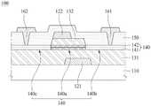
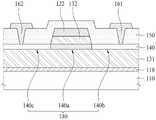
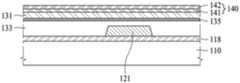
图1是图示出根据本公开的一个实施例的薄膜晶体管100的横截面视图。FIG. 1 is a cross-sectional view illustrating a
根据本公开的一个实施例的薄膜晶体管100包含(或包括)第一栅电极121、有源层140和第二栅电极122。The
有源层140被设置成与第一栅电极121(间)隔开。有源层140的至少一部分与第一栅电极121重叠。The
第二栅电极122与有源层140(间)隔开,并且基于有源层140与第一栅电极121相反地设置。换句话说,第二栅电极122基于有源层140设置在第一栅电极121的相反侧。即,第一栅电极121设置在有源层140的一侧,而第二栅电极122设置在有源层140的另一侧。The
有源层140包含沟道部分140a。沟道部分140a与第一栅电极121和第二栅电极122中的至少一个重叠。而且,第一栅电极121可以比第二栅电极122更宽,与第二栅电极122相比,第一栅电极121可以与沟道部分140a的更多部分重叠。The
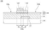
图2是图示出图1所示的薄膜晶体管100的沟道部分140a的局部横截面视图。FIG. 2 is a partial cross-sectional view illustrating the
将参考图1和2更详细地描述根据本公开的一个实施例的薄膜晶体管100。The
参考图1和2,第一栅电极121设置在基板110上。Referring to FIGS. 1 and 2 , the
玻璃或塑料可用作基板110的材料。具有柔性特性的透明塑料(例如,聚酰亚胺)可以用作塑料。当使用聚酰亚胺作为基板110的材料时,考虑到在基板110上执行高温沉积过程,可以使用在高温下可耐受的耐热聚酰亚胺。Glass or plastic may be used as the material of the
第一栅电极121可以包含诸如铝(Al)或铝合金的铝基金属、诸如银(Ag)或银合金的银基金属、诸如铜(Cu)或铜合金的铜基金属、诸如钼(Mo)或钼合金的钼基金属、铬(Cr)、钽(Ta)、钕(Nd)或钛(Ti)中的至少一种。第一栅电极121可以具有多层结构,该多层结构包含具有彼此不同的各自物理特性的至少两个导电层。The
第一栅绝缘层131设置在第一栅电极121上。第一栅绝缘层131可以具有绝缘特性,并且可以包含氧化硅、氮化硅或金属基氧化物中的至少一种。根据本公开的一个实施例,第一栅绝缘层131可以包含氮化硅。氮化硅包含与氧化硅和金属基氧化物相比相对更高浓度的氢。The first
第一栅绝缘层131可以具有单层结构,或者可以具有多层结构。The first
有源层140设置在第一栅绝缘层131上。The
根据本公开的一个实施例,有源层140包含氧化物半导体材料。有源层140可以由氧化物半导体层制成。According to one embodiment of the present disclosure, the
有源层140例如可以包含IZO(InZnO)基、IGO(InGaO)基、ITO(InSnO)基、IGZO(InGaZnO)基、IGZTO(InGaZnSnO)基、ITZO(InSnZnO)基、IGTO(InGaSnO)基、GO(GaO)基、GZTO(GaZnSnO)基和GZO(GaZnO)基氧化物半导体材料中的至少一种。然而,本公开的一个实施例不限于此示例,并且有源层140可以由本领域已知的其他氧化物半导体材料制成。The
有源层140包含沟道部分140a、分别设置在沟道部分140a的两侧的第一连接部分140b和第二连接部分140c。第一连接部分140b和第二连接部分140c彼此隔开并分别与沟道部分140a连接。The
第二栅绝缘层132设置在有源层140上。第二栅绝缘层132可以具有绝缘特性,并且可以包含氧化硅、氮化硅或金属基氧化物中的至少一种。第二栅绝缘层132可以具有单层结构,或者可以具有多层结构。The second
根据本公开的一个实施例,第二栅绝缘层132可以包含氧化硅。氧化硅可以包含与氮化硅相比相对更高浓度的氧。According to an embodiment of the present disclosure, the second
第二栅绝缘层132可以被图案化,或者可以不被图案化。图案化的第二栅绝缘层132可以至少覆盖有源层140的沟道部分140a,但是本公开的一个实施例不限于此。第二栅绝缘层132可以覆盖有源层140的整个上表面。The second
第二栅电极122设置在第二栅绝缘层132上。The
第二栅电极122可以由与第一栅电极121的材料相同的材料制成,或者可以由另一种材料制成。第二栅电极122基于有源层140设置在第一栅电极121的相反侧。例如,有源层140位于第一栅电极121与第二栅电极122之间。The
根据本公开的一个实施例,第一栅电极121的至少一部分与第二栅电极122不重叠,并且第二栅电极122的至少一部分与第一栅电极121不重叠。第一栅电极121的一部分和第二栅电极122的一部分可以彼此重叠。例如,第一栅电极121、沟道部分140a和第二栅电极122可以以交错型配置竖直(垂直)地层叠,其中第一栅电极121可以主要与沟道部分140a的大约一半重叠,第二栅电极122可以主要与与沟道部分140a的另一半重叠。According to an embodiment of the present disclosure, at least a portion of the
参考图1,层间介电层150设置在第二栅电极122上。层间介电层150可以由绝缘材料制成。Referring to FIG. 1 , an
源电极161和漏电极162设置在层间介电层150上。源电极161和漏电极162彼此隔开并与有源层140连接。The
参考图1,源电极161通过在层间介电层150中形成的接触孔与第一连接部分140b连接,漏电极162通过在层间介电层150中形成的另一接触孔与第二连接部分140c连接。与源电极161连接的第一连接部分140b可以被称为源极连接部分,与漏电极162连接的第二连接部分140c可以被称为漏极连接部分。Referring to FIG. 1 , the
根据本公开的一个实施例,第一连接部分140b和第二连接部分140c可以通过有源层140的选择性导电化而形成。例如,有源层140可以通过使用掺杂剂掺杂而被选择性地导电化,由此可以形成第一连接部分140b和第二连接部分140c。According to an embodiment of the present disclosure, the
对于掺杂,可以使用硼(B)离子、磷(P)离子或氟(F)离子中的至少一种。For doping, at least one of boron (B) ions, phosphorus (P) ions, or fluorine (F) ions may be used.
根据本公开的一个实施例,第一连接部分140b可以是漏极连接部分,第二连接部分140c可以是源极连接部分。另外,第一连接部分140b和第二连接部分140c中的任意一个可以是源电极,而第一连接部分140b和第二连接部分140c中的另一个可以是漏电极。According to an embodiment of the present disclosure, the
第一连接部分140b和第二连接部分140c可以用作线路。The
在下文中,将参考图2更详细地描述有源层140的沟道部分140a。Hereinafter, the
根据本公开的一个实施例,沟道部分140a与第一栅电极121和第二栅电极122中的至少一个重叠。当沟道部分140a的所有区域与第一栅电极121和第二栅电极122中的至少一个重叠时,可以确保沟道部分140a的连续性,例如,从沟道部分140a的一端、例如图2中所示的沟道部分140a的左侧到沟道部分140a的另一端、例如图2中所示的沟道部分140a的右侧(例如,沟道部分140a的所有部分可以与所述第一栅电极121或所述第二栅电极122中的至少一个重叠,从而允许沟道的全覆盖)。According to an embodiment of the present disclosure, the
参考图1和2,第一栅电极121的至少一部分与第二栅电极122不重叠,并且第二栅电极122的至少一部分与第一栅电极121不重叠。1 and 2 , at least a portion of the
由于第一栅电极121和第二栅电极122的配置(排布),沟道部分140a的一部分仅与第一栅电极121和第二栅电极122中的一个重叠,而沟道部分140a的另一部分仅与第一栅电极121和第二栅电极122中的另一个重叠。而且,沟道部分140a可以包含与第一栅电极121和第二栅电极122两者均重叠的中间部分。Due to the configuration (arrangement) of the
更详细地,参考图2,根据本公开的一个实施例的有源层140的沟道部分140a包含与第一栅电极121重叠但不与第二栅电极122重叠的第一沟道区域a1,以及与第二栅电极122重叠但不与第一栅极电极121重叠的第二沟道区域a2。In more detail, referring to FIG. 2 , the
结果是,沟道部分140a的第一沟道区域a1由第一栅电极121驱动,而沟道部分140a的第二沟道区域a2由第二栅电极122驱动。沟道部分140a的第一沟道区域a1是经受第一栅电极121影响的区域,而沟道部分140a的第二沟道区域a2经受第二栅电极122的影响。As a result, the first channel region a1 of the
参考图2,第一沟道区域a1定位于沟道部分140a的一端,并且第二沟道区域a2定位于沟道部分140a的另一端。根据本公开的一个实施例,如图2所示,第一连接部分140b可以与第一沟道区域a1接触,并且第二连接部分140c可以与第二沟道区域a2接触。2, the first channel region a1 is positioned at one end of the
参考图1和2,第一连接部分140b与第二栅电极122不重叠,并且第二连接部分140c与第一栅电极121不重叠。根据本公开的一个实施例,第一连接部分140b的至少一部分可以与第一栅电极121重叠。为了使第一栅电极121能够充分覆盖第一沟道区域a1,第一栅电极121可以具有比第一沟道区域a1更大的面积。结果是,第一连接部分140b的一部分可以与第一栅电极121重叠。尽管第一连接部分140b的一部分与第一栅电极121重叠,但是第一连接部分140b被导电化,因此不用作沟道。因此,即使存在第一连接部分140b与第一栅电极121重叠的区域,薄膜晶体管100的驱动也不受重叠区域的影响。Referring to FIGS. 1 and 2 , the
另一方面,根据本公开的一个实施例,第一连接部分140b可以不与第二栅电极122重叠。第二栅电极122是在有源层140的选择性导电化过程期间用作掩模的图案的一部分。因此,第二栅电极122可以不与第一连接部分140b和第二连接部分140c重叠。On the other hand, according to an embodiment of the present disclosure, the
根据本公开的一个实施例,第一栅电极121的一部分和第二栅电极122的一部分可以彼此重叠。因此,沟道部分140a的一部分可以与第一栅电极121和第二栅电极122两者均重叠。According to an embodiment of the present disclosure, a portion of the
根据本公开的一个实施例,沟道部分140a可以包含与第一栅电极121和第二栅电极122两者均重叠的第三沟道区域a3。第三沟道区域a3是经受第一栅电极121和第二栅电极122两者影响的区域。According to one embodiment of the present disclosure, the
为了确保沟道部分140a的连续性,沟道部分140a需要与第一栅电极121和第二栅电极122中的至少一个重叠,并且考虑到第一栅电极121和第二栅电极122的制造过程中的过程误差,第一栅电极121和第二栅电极122可以被设计成彼此部分地重叠。根据本公开的一个实施例,第三沟道区域a3的长度可以设计得尽可能小。In order to ensure the continuity of the
当第三沟道区域a3存在于沟道部分140a中时,可以确保沟道部分140a从沟道部分140a的一端到沟道部分140a的另一端的连续性。When the third channel region a3 exists in the
根据本公开的一个实施例,有源层140包含第一有源层141和第一有源层141上的第二有源层142。参考图1和2,第一有源层141设置在第一栅绝缘层131上,第二有源层142设置在第一有源层141上。第一有源层141和第二有源层142分别为氧化物半导体材料层。构成第一有源层141和第二有源层142的氧化物半导体材料可以包含金属和氧。根据本公开的一个实施例,第一有源层141和第二有源层142可以具有相同的金属成分(组分)。根据本公开的一个实施例,第一有源层141和第二有源层142具有相同的金属成分,并且可以通过氧和氢中的至少一种的含量差异来彼此区分。According to an embodiment of the present disclosure, the
根据本公开的一个实施例,第一有源层141和第二有源层142中的任意一个具有比第一有源层141和第二有源层142中的另一个更高的氢浓度和更低的氧浓度。According to one embodiment of the present disclosure, any one of the first
例如,第一有源层141可具有高于第二有源层142的氢浓度的氢浓度,且可具有低于第二有源层142的氧浓度的氧浓度。第二有源层142可具有低于第一有源层141的氢浓度的氢浓度,且可具有高于第一有源层141的氧浓度的氧浓度。For example, the first
根据本公开的一个实施例,与第二有源层142相比,第一有源层141包含过量的氢(H)。第一有源层141可以是具有比用作薄膜晶体管的沟道的传统氧化物半导体材料层更高的氢浓度的过量氢层。According to an embodiment of the present disclosure, the first
当第一有源层141包含过量氢时,由于氢(H)的电离效应而发生空穴陷阱效应,由此薄膜晶体管100的阈值电压可沿负(-)方向移动。因此,阈值电压Vth可沿负(-)方向偏移(移位)。When the first
根据本公开的一个实施例,与第一有源层141相比,第二有源层142包含过量的氧(O)。第二有源层142可以是具有比用作薄膜晶体管的沟道的传统氧化物半导体材料更高的氧浓度的过量氧层。According to an embodiment of the present disclosure, the second active layer 142 contains an excess of oxygen (O) compared to the first
当第二有源层142包含过量氧时,会发生电子陷阱效应,由此薄膜晶体管100的阈值电压可沿正(+)方向移动。因此,阈值电压Vth可沿正(+)方向偏移。When the second active layer 142 contains excess oxygen, an electron trap effect occurs, whereby the threshold voltage of the
根据本公开的一个实施例的薄膜晶体管100可同时具有由于含有过量氢的层而导致的阈值电压Vth的负(-)偏移效应和由于含有过量氧的层而导致的阈值电压Vth的正(+)偏移效应,因而即使随着时间的推移(流逝)也可以抑制薄膜晶体管100的阈值电压Vth的变化。The
在本公开的一个实施例中,氧化物半导体材料层具有“过量氧”的情况意味着氧比率高于构成氧化物半导体的金属和氧以化学计量方式形成稳定化学键时的氧比率。In one embodiment of the present disclosure, the case where the oxide semiconductor material layer has "excess oxygen" means that the oxygen ratio is higher than when the metal and oxygen constituting the oxide semiconductor form a stable chemical bond stoichiometrically.
将通过示例的方式来描述In、Ga和Zn以1:1:1的比率包含在IGZO(InGaZnO)基氧化物半导体中的情况。The case where In, Ga, and Zn are contained in an IGZO (InGaZnO)-based oxide semiconductor at a ratio of 1:1:1 will be described by way of example.
铟(In)可以以In2O3的状态与氧结合。镓(Ga)可以以Ga2O3的状态与氧结合。另外,锌(Zn)可以以ZnO的状态与氧结合。因此,当In、Ga和Zn的化学计量比为1:1:1时,与其对应的氧的化学计量比为1.5:1.5:1。结果是,当In、Ga和Zn以1:1:1的比率使用时,氧的化学计量比变为4。在这种情况下,In、Ga、Zn和O的化学计量比为1:1:1:4(In:Ga:Zn:O=1:1:1:4),而氧的化学计量比可以为4。因此,氧化物半导体材料层具有“过量氧”的情况意味着当In、Ga和Zn的化学计量比为1:1:1时,氧的化学计量比超过4。这可由以下方程式1表示。Indium (In) may be combined with oxygen in the state of In2 O3 . Gallium (Ga) may be combined with oxygen in the state of Ga2 O3 . In addition, zinc (Zn) may be combined with oxygen in the state of ZnO. Therefore, when the stoichiometric ratio of In, Ga, and Zn is 1:1:1, the stoichiometric ratio of their corresponding oxygen is 1.5:1.5:1. As a result, when In, Ga and Zn are used in a ratio of 1:1:1, the stoichiometric ratio of oxygen becomes 4. In this case, the stoichiometric ratio of In, Ga, Zn, and O is 1:1:1:4 (In:Ga:Zn:O=1:1:1:4), while the stoichiometric ratio of oxygen can be is 4. Therefore, the case where the oxide semiconductor material layer has "excessive oxygen" means that the stoichiometric ratio of oxygen exceeds 4 when the stoichiometric ratio of In, Ga, and Zn is 1:1:1. This can be represented by
[方程式1][Equation 1]
InGaZnO4+x(其中,x>0)InGaZnO4+x (where x>0)
一般地,过量的氢可被描述为乏氧部分。例如,在其中In、Ga和Zn的化学计量比为1:1:1的氧化物半导体层中,当氧的化学计量含量小于4时,可以将其描述为乏氧状态。例如,可以通过方程式2来描述乏氧状态。In general, excess hydrogen can be described as an oxygen-deficient fraction. For example, in an oxide semiconductor layer in which the stoichiometric ratio of In, Ga, and Zn is 1:1:1, when the stoichiometric content of oxygen is less than 4, it can be described as an oxygen-deficient state. For example, the hypoxic state can be described by Equation 2.
[方程式2][Equation 2]
InGaZnO4-y(其中,y>0)InGaZnO4-y (wherein, y>0)
一般地,氧化物半导体层中因氧的缺乏而产生的间隙可以由氢(H)填充。氧化物半导体材料层具有“过量氢”的情况意味着氧化物半导体含有比稳定的乏氧状态更多的氢。根据本公开的一个实施例,当氢含量是乏氧的至少两倍时,氧化物半导体层可以被称为氢过量状态。更详细地,在方程式2中,当氢的化学计量含量为2y或更高时,氧化物半导体层可以被称为氢过量状态。In general, gaps in the oxide semiconductor layer due to lack of oxygen may be filled with hydrogen (H). The fact that the oxide semiconductor material layer has "excess hydrogen" means that the oxide semiconductor contains more hydrogen than a stable oxygen-deficient state. According to an embodiment of the present disclosure, when the hydrogen content is at least twice that of the oxygen-deficient state, the oxide semiconductor layer may be referred to as a hydrogen excess state. In more detail, in Equation 2, when the stoichiometric content of hydrogen is 2y or more, the oxide semiconductor layer may be referred to as a hydrogen excess state.
参考图2,沟道部分140a的第一沟道区域a1由第一栅电极121驱动,并且第一沟道区域a1中的第一有源层141被设置成比第二有源层142更靠近第一栅电极121。因此,沟道部分140a的第一沟道区域a1的驱动主要经受(或受到)第一有源层141的影响。结果是,当第一有源层141具有比第二有源层142更高的氢浓度和更低的氧浓度时,第一沟道区域a1可用于能够使薄膜晶体管100的阈值电压沿负(-)方向移动。2, the first channel region a1 of the
沟道部分140a的第二沟道区域a2由第二栅电极122驱动,并且第二沟道区域a2中的第二有源层142被设置成比第一有源层141更靠近第二栅电极122。因此,沟道部分140a的第二沟道区域a2的驱动主要经受(或受到)第二有源层142的影响。结果是,当第二有源层142具有比第一有源层141更高的氧浓度和更低的氢浓度时,第二沟道区域a2可用于能够使薄膜晶体管100的阈值电压沿正(+)方向移动。The second channel region a2 of the
如上所述,根据本公开的一个实施例的薄膜晶体管100的沟道部分140a包含用于使阈值电压沿负(-)方向偏移的第一沟道区域a1和用于使阈值电压Vth沿正(+)方向偏移的第二沟道区域a2。因此,在根据本公开的一个实施例的薄膜晶体管100中,阈值电压Vth沿负(-)方向的偏移效应和阈值电压Vth沿正(+)方向的偏移效应被抵消,由此可以抑制阈值电压Vth的变化。因此,根据本公开的一个实施例的薄膜晶体管100可以在阈值电压Vth没有大的变化的情况下被稳定地驱动。特别地,即使在薄膜晶体管长时间在接通状态下被驱动的情况下,薄膜晶体管也可以阈值电压没有变化的情况下被稳定地驱动。例如,由于这种独特的设计,即使在所述装置已经被长时间使用之后,所实施的本发明也可以有效地将阈值电压Vth设定(或定置)为特定值并将其保持在那里。As described above, the
然而,本公开的一个实施例不限于上述示例,并且第一有源层141可以具有比第二有源层142更低的氢浓度和更高的氧浓度,而第二有源层142可以具有比第一有源层141更高的氢浓度和更低的氧浓度(参考图4B和5B)。However, one embodiment of the present disclosure is not limited to the above examples, and the first
参考图2,沟道部分140a的第一沟道区域a1由第一栅电极121驱动,并且包含在第一沟道区域a1中的第一有源层141被设置成比第二有源层142更靠近第一栅电极121。因此,沟道部分140a的第一沟道区域a1的驱动主要经受第一有源层141的影响。结果是,当第一有源层141具有比第二有源层142更低的氢浓度和更高的氧浓度时,第一沟道区域a1可用于能够使薄膜晶体管301或401的阈值电压沿正(+)方向移动。Referring to FIG. 2, the first channel region a1 of the
沟道部分140a的第二沟道区域a2由第二栅电极122驱动,并且包含在第二沟道区域a2中的第二有源层142被设置成比第一有源层141更靠近第二栅电极122。因此,沟道部分140a的第二沟道区域a2主要经受第二有源层142的影响。结果是,当第二有源层142具有比第一有源层141更高的氢浓度和更低的氧浓度时,第二沟道区域a2可用于能够使薄膜晶体管301或401的阈值电压沿负(-)方向移动。The second channel region a2 of the
如上所述,根据本公开的一个实施例的薄膜晶体管301或401的沟道部分140a包含用于使阈值电压Vth沿正(+)方向偏移的第一沟道区域a1和用于使阈值电压Vth沿负(-)方向偏移的第二沟道区域a2(参考图4B和5B)。因此,在根据本公开的一个实施例的薄膜晶体管301或401中,阈值电压Vth沿正(+)方向的偏移效应和阈值电压Vth沿负(-)方向的偏移效应被抵消,由此可以抑制阈值电压Vth的变化。因此,根据本公开的一个实施例的薄膜晶体管301或401可以在阈值电压Vth没有大的变化的情况下被稳定地驱动。As described above, the
如上所述,根据本公开的一个实施例,第一有源层141可以具有比第二有源层142更高的氢浓度和更低的氧浓度,以及第一有源层141可以具有比第二有源层142更低的氢浓度和更高的氧浓度。由于第一有源层141和第二有源层142的氢浓度与氧浓度之间的差异以及第一栅电极121和第二栅电极122的配置特性,根据本公开的一个实施例的薄膜晶体管100可以在阈值电压Vth没有变化的情况下具有优异的稳定性。As described above, according to one embodiment of the present disclosure, the first
可以以各种方式调整第一有源层141和第二有源层142的氢浓度和氧浓度。The hydrogen and oxygen concentrations of the first
例如,可以适当地选择在第一有源层141和第二有源层142的制造过程中使用的材料,以便可以调整第一有源层141和第二有源层142的氢浓度和氧浓度。For example, the materials used in the manufacturing process of the first
根据本公开的一个实施例,第一有源层141和第二有源层142可以通过金属有机化学气相沉积(MOCVD)方法形成。此时,可以通过调整在MOCVD方法中使用的氢气(H2)或臭氧(O3)的含量来调整第一有源层141和第二有源层142的氢浓度和氧浓度。According to an embodiment of the present disclosure, the first
可以通过在第一有源层141或第二有源层142附近设置供氢层或通过利用氧处理(例如,利用N2O气体)对第一有源层141或第二有源层142进行处理来调整第一有源层141和第二有源层142的氢浓度和氧浓度。The first
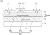
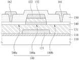
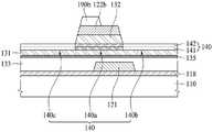
图3是图示出根据本公开的另一实施例的薄膜晶体管200的横截面视图。在下文中,为了避免冗余,将省略对已描述元件的描述。FIG. 3 is a cross-sectional view illustrating a
参考图3,第二栅绝缘层132可以覆盖有源层140的整个上表面。在图3中,有源层140的朝向第二栅电极122的表面被称为上表面。根据本公开的另一实施例,第二栅绝缘层132可以不被图案化。Referring to FIG. 3 , the second
参考图3,可以在第二栅绝缘层132中形成接触孔。Referring to FIG. 3 , a contact hole may be formed in the second
根据本公开的另一实施例,源电极161可以通过在层间介电层150和第二栅绝缘层132中形成的接触孔与有源层140的第一连接部分140b连接。漏电极162可以通过在层间介电层150和第二栅绝缘层132中形成的另一接触孔与有源层140的第二连接部分140c连接。According to another embodiment of the present disclosure, the
图4A是图示出根据本公开的又一实施例的薄膜晶体管300的横截面视图。根据本公开的另一实施例的薄膜晶体管300包含设置在第一栅电极121与有源层140之间的供氢层135。FIG. 4A is a cross-sectional view illustrating a
参考图4A,缓冲层118可以设置在基板110上。缓冲层118可以包含氧化硅和氮化硅中的至少一种。缓冲层118可以保护有源层140,并且可以具有平坦(平面)化特性,以使基板110的上部平坦化。Referring to FIG. 4A , the
第一栅电极121设置在缓冲层118上,并且第一钝化层133设置在第一栅电极121上。第一钝化层133可以起到绝缘和保护第一栅电极121的作用。第一钝化层133可由与第一栅绝缘层131的材料相同的材料制成。The
供氢层135设置在第一钝化层133上。供氢层135向有源层140供应氢。结果是,可以形成含有比第二有源层142更高的浓度的氢的第一有源层141。第一有源层141含有浓度高于氧化物半导体层的典型氢浓度的氢。根据本公开的另一实施例的第一有源层141是含有过量氢的过量氢层。The
供氢层135例如可由氮化硅(SiNx)形成。用作供氢层135的氮化硅(SiNx)层可以包含高浓度的氢。The
第一栅绝缘层131设置在供氢层135上。第一栅绝缘层131可以具有绝缘特性,并且可以包含氧化硅、氮化硅和金属基氧化物中的至少一种。第一栅绝缘层131可由与第一钝化层133的材料相同的材料形成。第一栅绝缘层131和第一钝化层133可以统称为第一栅绝缘层或下栅绝缘层。The first
有源层140设置在第一栅绝缘层131上,并且第二栅绝缘层132设置在有源层140上。The
第二栅电极122设置在第二栅绝缘层132上,并且层间介电层150设置在第二栅电极122上。源电极161和漏电极162设置在层间介电层150上。The
然而,本公开的又一实施例并不限于图4A中所示的构造(或配置)。根据本公开的又一实施例,供氢层135可以设置在有源层140上方。例如,供氢层135可以设置在第二栅绝缘层132中,或者可以设置在层间介电层150中。However, yet another embodiment of the present disclosure is not limited to the configuration (or configuration) shown in FIG. 4A . According to yet another embodiment of the present disclosure, the
图4B是图示出根据本公开的又一实施例的薄膜晶体管301的横截面视图。参考图4B,供氢层135可以设置在第二栅绝缘层132上。如图4B中所描绘,当供氢层135设置在有源层140上方时,第二有源层142可以包含过量的氢。FIG. 4B is a cross-sectional view illustrating a
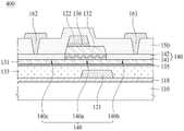
图5A是图示出根据本公开的再一实施例的薄膜晶体管的横截面视图。与图4A的薄膜晶体管300相比,图5A的薄膜晶体管400进一步包含供氧层136。5A is a cross-sectional view illustrating a thin film transistor according to still another embodiment of the present disclosure. Compared with the
详细地,根据本公开的又一实施例的薄膜晶体管400包含设置在有源层140与第二栅电极122之间的供氧层136。供氧层136向有源层140供应氧。结果是,可以形成含有浓度高于第一有源层141的浓度的氧的第二有源层142。第二有源层142可以包含浓度高于典型氧化物半导体层的氧浓度的氧。根据本公开的又一实施例的第二有源层142是含有过量氧的过量氧层。In detail, the
图5B是图示出根据本公开的再一实施例的薄膜晶体管的横截面视图。图5B的薄膜晶体管401包含供氢层135和供氧层136。FIG. 5B is a cross-sectional view illustrating a thin film transistor according to still another embodiment of the present disclosure. The
参考图5B,供氧层136可以设置在第一钝化层133上。供氧层136可以向有源层140的下部供应氧。结果是,第一有源层141可以具有比第二有源层142更高的氧浓度。Referring to FIG. 5B , an
第一栅绝缘层131设置在供氧层136上,并且有源层140设置在第一栅绝缘层131上。第二栅绝缘层132设置在有源层140上,并且第二栅电极122设置在第二栅绝缘层132上。The first
参考图5B,供氢层135可以设置在第二栅绝缘层132中。供氢层135可以向有源层140的上部供应氢。结果是,第二有源层142可以具有比第一有源层141更高的氢浓度。第二栅绝缘层132可基于供氢层135被分为下层132a和上层132b。例如,供氢层135可以设置在第二栅绝缘层132的下层132a和上层132b之间。Referring to FIG. 5B , the
在根据本公开的再一实施例的图5B所示的薄膜晶体管401中,第一有源层141可以具有比第二有源层142更高的氧浓度,以及第二有源层142可以具有比第一有源层141更高的氢浓度。In the
图6是图示出根据本公开的再一实施例的薄膜晶体管500的横截面视图。FIG. 6 is a cross-sectional view illustrating a
参考图6,供氢层135设置在第一栅电极121上。供氢层135向有源层140的预定区域供应氢。结果是,定位于第一有源层141的供氢层135上方的第一区域141a1可以具有比第一有源层141的其他区域更高的氢浓度。Referring to FIG. 6 , the
更详细地,第一有源层141具有与第一栅电极121重叠的第一区域141a1,其中第一区域141a1具有比第一有源层141的其他区域更高的氢浓度。In more detail, the first
参考图6,第二有源层142可以具有第二区域142a2。第二有源层142的第二区域142a2与第二栅电极122重叠。第二区域142a2可以具有高于第二有源层142的其他区域的氧浓度的氧浓度。Referring to FIG. 6 , the second active layer 142 may have a second region 142a2. The second region 142a2 of the second active layer 142 overlaps with the
例如,根据本公开的再一实施例,可以选择性地对第二有源层142进行氧处理,以在第二有源层142中形成第二区域142a2。For example, according to still another embodiment of the present disclosure, the second active layer 142 may be selectively subjected to oxygen treatment to form the second region 142a2 in the second active layer 142.
参考图6,根据本公开的再一实施例的薄膜晶体管500具有设置在第二栅绝缘层132与第二栅电极122之间的供氧层136。供氧层136可以向第二有源层142供应氧,以在第二有源层142中形成第二区域142a2。例如,氧和氢可以集中于薄膜晶体管的沟道部分140a的相反角部/侧。Referring to FIG. 6 , a
图7和8是图示出根据比较示例的薄膜晶体管的横截面视图。在下文中,图7所示的薄膜晶体管将被称为比较示例1,图8所示的薄膜晶体管将被称为比较示例2。7 and 8 are cross-sectional views illustrating thin film transistors according to comparative examples. Hereinafter, the thin film transistor shown in FIG. 7 will be referred to as Comparative Example 1, and the thin film transistor shown in FIG. 8 will be referred to as Comparative Example 2.
如图7所示,根据比较示例1的薄膜晶体管不包含第一栅电极121,而仅包含第二栅电极122。图7所示的薄膜晶体管也被称为顶栅结构的薄膜晶体管。As shown in FIG. 7 , the thin film transistor according to Comparative Example 1 does not include the
图7所示的薄膜晶体管的沟道部分140a仅与一个栅电极重叠。因此,图7所示的薄膜晶体管不包含其中沟道部分140a的一部分仅与第一栅电极121和第二栅电极122中的一个重叠而沟道部分140a的另一部分仅与第一栅电极121和第二栅电极122中的另一个重叠的构造。The
根据图8所示的比较示例2的薄膜晶体管包含第一栅电极121和第二栅电极122两者。图8所示的薄膜晶体管也被称为双栅结构的薄膜晶体管。The thin film transistor according to Comparative Example 2 shown in FIG. 8 includes both the
在图8所示的薄膜晶体管中,沟道部分140a的整个区域与第一栅电极121和第二栅电极122重叠。因此,图8所示的薄膜晶体管不包含其中沟道部分140a的一部分仅与第一栅电极121和第二栅电极122中的一个重叠而沟道部分140a的另一部分仅与第一栅电极121和第二栅电极122中的另一个重叠的构造。In the thin film transistor shown in FIG. 8 , the entire region of the
具有图7或8所示构造的薄膜晶体管具有阈值电压Vth的变化,其大于根据本公开的实施例的薄膜晶体管100、200、300、301、400、401和500中的每一个的变化。The thin film transistor having the configuration shown in FIG. 7 or 8 has a variation in threshold voltage Vth greater than that of each of the
图9是图示出阈值电压Vth的变化的曲线图。FIG. 9 is a graph illustrating changes in the threshold voltage Vth.
在图9所示曲线图的中心处的曲线中,阈值电压Vth接近于0V。另一方面,在图9所示曲线图的左侧的曲线中,阈值电压沿负(-)电压方向偏移。如在图9中的曲线图的左侧的曲线中所示,当阈值电压沿负(-)电压方向偏移时,阈值电压Vth沿负(-)方向偏移。In the curve at the center of the graph shown in FIG. 9, the threshold voltage Vth is close to 0V. On the other hand, in the graph on the left side of the graph shown in FIG. 9 , the threshold voltage is shifted in the negative (-) voltage direction. As shown in the graph on the left side of the graph in FIG. 9 , when the threshold voltage is shifted in the negative (-) voltage direction, the threshold voltage Vth is shifted in the negative (-) direction.
在图9所示曲线图的右侧的曲线中,阈值电压沿正(+)电压方向偏移。如在图9中的曲线图的右侧的曲线中所示,当阈值电压沿正(+)电压方向偏移时,阈值电压Vth沿正(+)方向偏移。In the graph on the right side of the graph shown in FIG. 9, the threshold voltage is shifted in the positive (+) voltage direction. As shown in the graph on the right side of the graph in FIG. 9 , when the threshold voltage is shifted in the positive (+) voltage direction, the threshold voltage Vth is shifted in the positive (+) direction.
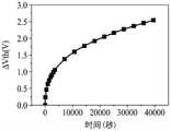
图10A、10B和10C是图示出阈值电压随时间的变化的曲线图。详细地,图10A、10B和10C表示正偏压温度应力(PBTS)测试的结果。10A, 10B and 10C are graphs illustrating changes in threshold voltage with time. In detail, FIGS. 10A , 10B and 10C represent the results of a positive bias temperature stress (PBTS) test.
PBTS是指施加正(+)偏置电压和恒定温度条件下的应力。当PBTS增加时,氧化物半导体层120或薄膜晶体管100中的应力增加,由此阈值电压的变化量ΔVth(或变化率)可能增加。PBTS refers to stress under conditions of application of a positive (+) bias voltage and constant temperature. When the PBTS is increased, the stress in the oxide semiconductor layer 120 or the
在图10A中,在将PBTS施加于根据图7所示的比较示例1的薄膜晶体管的状态下,测量阈值电压Vth随时间的变化量ΔVth。参考图10A,应注意的是,当将PBTS施加于图7所示的薄膜晶体管(比较示例1)时,阈值电压Vth的变化量随着时间的推移而不断增加。在图7所示的薄膜晶体管(比较示例1)中,应注意的是,当施加PBTS时,阈值电压Vth不断增加,而不会收敛于某个特定(具体)值,并且在40,000秒之后,阈值电压的变化量ΔVth为0.254V左右。In FIG. 10A , in a state where the PBTS is applied to the thin film transistor according to Comparative Example 1 shown in FIG. 7 , the amount of change ΔVth of the threshold voltage Vth with time is measured. Referring to FIG. 10A , it should be noted that when PBTS is applied to the thin film transistor shown in FIG. 7 (Comparative Example 1), the amount of change in threshold voltage Vth increases with time. In the thin film transistor shown in FIG. 7 (Comparative Example 1), it should be noted that when PBTS is applied, the threshold voltage Vth keeps increasing without converging to a certain (specific) value, and after 40,000 seconds, The change amount ΔVth of the threshold voltage is about 0.254V.
在图10B中,在将PBTS施加于根据图8所示的比较示例2的薄膜晶体管的状态下,测量阈值电压Vth随时间的变化量ΔVth。参考图10B,应注意的是,当将PBTS施加于图8所示的薄膜晶体管(比较示例2)时,阈值电压Vth的变化量随着时间的推移而不断增加。在图8所示的薄膜晶体管(比较示例2)中,应注意的是,当施加PBTS时,阈值电压Vth不断增加,而不会收敛于某个特定(具体)值,并且在40,000秒之后,阈值电压的变化量ΔVth为2.54V左右。In FIG. 10B , in a state where the PBTS is applied to the thin film transistor according to Comparative Example 2 shown in FIG. 8 , the amount of change ΔVth of the threshold voltage Vth with time is measured. Referring to FIG. 10B , it should be noted that when PBTS is applied to the thin film transistor shown in FIG. 8 (Comparative Example 2), the amount of change in threshold voltage Vth increases with time. In the thin film transistor shown in FIG. 8 (Comparative Example 2), it should be noted that when PBTS is applied, the threshold voltage Vth keeps increasing without converging to a certain (specific) value, and after 40,000 seconds, The change amount ΔVth of the threshold voltage is about 2.54V.
根据图8所示的比较示例2的薄膜晶体管由于其双栅结构而可以具有优异的开电流特性,但具有阈值电压Vth的变化量ΔVth随着时间的推移而增加的问题。The thin film transistor according to Comparative Example 2 shown in FIG. 8 can have excellent on-current characteristics due to its double gate structure, but has a problem that the variation amount ΔVth of the threshold voltage Vth increases with time.
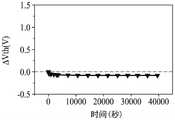
图10C是图示出根据图4A所示的本公开的另一实施例的薄膜晶体管300的阈值电压的曲线图。参考图10C,应注意的是,即使将PBTS施加于根据本公开的另一实施例的薄膜晶体管300,阈值电压Vth也几乎没有变化。因此,与图7和图8的示例构造相比,所实施的本发明的特定类型的交错、双栅构造提供了随时间稳定得多的阈值电压。FIG. 10C is a graph illustrating the threshold voltage of the
在下文中,将参考图11A-11M来描述制造根据本公开的另一实施例的薄膜晶体管300的方法。Hereinafter, a method of manufacturing a
图11A-11M是图示出制造根据本公开的另一实施例的薄膜晶体管300的方法的过程视图。11A-11M are process views illustrating a method of manufacturing a
参考图11A,在基板110上形成缓冲层118,以及在缓冲层118上形成第一栅电极121。Referring to FIG. 11A , a
参考图11B,在第一栅电极121上形成第一钝化层133,在第一钝化层133上形成供氢层135,以及在供氢层135上形成第一栅绝缘层131。11B , a
第一钝化层133可由绝缘材料制成。供氢层135是用于向随后将描述的有源层140供应氢的层。供氢层135例如可由氮化硅(SiNx)形成。施加于供氢层135的氮化硅(SiNx)层可以包含高浓度的氢。第一栅绝缘层131具有绝缘特性。The
参考图11C,在第一栅绝缘层131上形成有源层140。有源层140包含氧化物半导体材料。有源层140可以是氧化物半导体层。有源层140例如可以包含IZO(InZnO)基、IGO(InGaO)基、ITO(InSnO)基、IGZO(InGaZnO)基、IGZTO(InGaZnSnO)基、ITZO(InSnZnO)基、IGTO(InGaSnO)基、GO(GaO)基、GZTO(GaZnSnO)基和GZO(GaZnO)基氧化物半导体材料中的至少一种。Referring to FIG. 11C , an
参考图11D,对有源层140的表面进行氧处理。图11D所示的氧处理可以包含利用N2O气体处理有源层140的表面。Referring to FIG. 11D , oxygen treatment is performed on the surface of the
通过供氢层135将氢供应到有源层140,并且通过氧处理将氧(O)供应到有源层140的表面,由此可以形成第一有源层141和第二有源层142。The first
结果是,如图11E所示,形成包含第一有源层141和第二有源层142的有源层140。第一有源层141可以具有比第二有源层142更高的氢浓度和更低的氧浓度。此外,第二有源层142可以具有比第一有源层141更低的氢浓度和更高的氧浓度。As a result, as shown in FIG. 11E , the
然而,本公开的另一实施例不限于上述示例,并且第一有源层141可以具有比第二有源层142更低的氢浓度和更高的氧浓度,而第二有源层142可以具有比第一有源层141更高的氢浓度和更低的氧浓度。However, another embodiment of the present disclosure is not limited to the above examples, and the first
例如,第一有源层141和第二有源层142可以通过金属有机化学气相沉积(MOCVD)方法形成。此时,可以通过调整在MOCVD方法中使用的氢气(H2)或臭氧(O3)的含量来调整第一有源层141和第二有源层142的氢浓度和氧浓度。通过增加在形成第一有源层141时使用的臭氧(O3)的量和增加在形成第二有源层142时使用的氢的量,第一有源层141可以具有比第二有源层142更低的氢浓度和更高的氧浓度。For example, the first
参考图11F,在有源层140上形成第二栅绝缘层132,以及在第二栅绝缘层132上形成第二栅电极材料层122a。第二栅电极材料层122a可以包含诸如铝(Al)或铝合金的铝基金属、诸如银(Ag)或银合金的银基金属、诸如铜(Cu)或铜合金的铜基金属、诸如钼(Mo)或钼合金的钼基金属、铬(Cr)、钽(Ta)、钕(Nd)和钛(Ti)中的至少一种。第二栅电极材料层122a可以具有多层结构,该多层结构包含具有彼此不同的各自物理特性的至少两个导电层。Referring to FIG. 11F , a second
参考图11G,在第二栅电极材料层122a上形成第一光刻胶(光致抗蚀剂)图案190a。第一光刻胶图案190a可以通过光刻胶的曝光和显影形成。Referring to FIG. 11G, a first photoresist (photoresist)
参考图11H,使用第一光刻胶图案190a作为掩模来蚀刻第二栅电极材料层122a。结果是,形成第二栅电极图案122b。Referring to FIG. 11H, the second gate
参考图11I,可以通过使用第二栅电极图案122b作为掩模进行蚀刻来图案化第二栅绝缘层132。此时,第一光刻胶图案190a的一部分被移除,以形成第二光刻胶图案190b。Referring to FIG. 11I, the second
然而,本公开的另一实施例不限于上述示例,并且第二栅绝缘层132可以不被图案化。However, another embodiment of the present disclosure is not limited to the above examples, and the second
参考图11J,有源层140被选择性地导电化(处理)。例如,可以在有源层140上选择性地掺杂掺杂剂。图11J示例性地图示出了通过掺杂使有源层140选择性地导电化的过程。Referring to FIG. 11J, the
参考图11J,可以通过使用第二栅电极图案122b作为掩模进行掺杂来使有源层140选择性地导电化。不受第二栅电极图案122b保护的有源层140的区域被选择性地导电化。Referring to FIG. 11J, the
掺杂剂可以包含硼(B)、磷(P)和氟(F)中的至少一种。掺杂剂可以以离子态掺杂。根据本公开的一个实施例,导电化可以通过离子注入进行离子掺杂而进行。The dopant may contain at least one of boron (B), phosphorus (P), and fluorine (F). The dopant can be doped in an ionic state. According to one embodiment of the present disclosure, the conduction may be performed by ion doping by ion implantation.
参考图11K,作为使用第二栅电极图案122b作为掩模对有源层140进行选择性导电化处理的结果,形成第一连接部分140b和第二连接部分140c。参考图11K,第二连接部分140c的至少一部分可以与第一栅电极121重叠。为了使第一栅电极121充分覆盖如图2中所示的第一沟道区域a1,第一栅电极121可以具有比第一沟道区域a1更大的面积。结果是,第一连接部分140b的一部分可以与第一栅电极121重叠。尽管第一连接部分140b的一部分与第一栅电极121重叠,但是第一连接部分140b已被导电化,因此不用作沟道。因此,即使存在第一连接部分140b与第一栅电极121重叠的区域,薄膜晶体管300的驱动也不受重叠区域的影响。Referring to FIG. 11K, as a result of the selective conduction process of the
根据本公开的一个实施例,有源层140的沟道部分140a未被导电化。第二栅电极图案122b用作在导电化过程期间保护沟道部分140a的掩模。According to an embodiment of the present disclosure, the
参考图11L,通过使用第二光刻胶图案190b作为掩模进行蚀刻来蚀刻第二栅电极图案122b,由此形成第二栅电极122。在形成第二栅电极122之后,移除第二光刻胶图案190b。Referring to FIG. 11L, the second
根据本公开的另一实施例,第一栅电极121的至少一部分与第二栅电极122不重叠,并且第二栅电极122的至少一部分被形成为不与第一栅电极121重叠。第一栅电极121可以与第二栅电极122的一部分重叠。According to another embodiment of the present disclosure, at least a portion of the
沟道部分140a被形成为与第一栅电极121和第二栅电极122中的至少一个重叠。The
另外,第一栅电极121的至少一部分被形成为不与第二栅电极122重叠,并且第二栅电极122的至少一部分被形成为不与第一栅电极121重叠。In addition, at least a portion of the
根据本公开的另一实施例,沟道部分140a被设计为使得其一部分仅与第一栅电极121和第二栅电极122中的一个重叠,而其另一部分仅与第一栅电极121和第二栅电极122中的另一个重叠。According to another embodiment of the present disclosure, the
参考图11M,在第二栅电极122上形成层间介电层150,并且在层间介电层150上设置源电极161和漏电极162。源电极161和漏电极162彼此隔开并与有源层140连接。Referring to FIG. 11M , an
参考图11M,在形成源电极161和漏电极162之前,可以在层间介电层150中形成接触孔。源电极161通过在层间介电层150中形成的接触孔与第一连接部分140b连接,漏电极162通过在层间介电层150中形成的另一接触孔与第二连接部分140c连接。Referring to FIG. 11M , before forming the
根据本公开的实施例的薄膜晶体管100、200、300、301、400、401和500可以有效(有用)地应用于显示装置。特别地,根据本公开的实施例的薄膜晶体管100、200、300、301、400、401和500可以有效地应用于长时间在接通状态下驱动的户外显示装置或使用微型LED的显示装置。The
图12是图示出根据本公开的另一实施例的显示装置600的示意性视图。FIG. 12 is a schematic view illustrating a
如图12所示,根据本公开的另一实施例的显示装置600包含显示面板310、栅极驱动器320、数据驱动器330和控制器340。As shown in FIG. 12 , a
显示面板310包含栅极线GL、数据线DL、设置在栅极线GL与数据线DL之间的交叉区域中的像素P。像素P包含显示元件710和用于驱动显示元件710的像素驱动电路PDC。通过驱动像素P在显示面板310上显示图像。The
控制器340控制栅极驱动器320和数据驱动器330。The
控制器340通过使用从外部系统(未示出)提供的同步信号和时钟信号来输出用于控制栅极驱动器320的栅极控制信号GCS和用于控制数据驱动器330的数据控制信号DCS。此外,控制器340对从外部系统输入的输入图像数据进行采样,重新排列采样的数据,并将重新排列的数字图像数据RGB提供给数据驱动器330。The
栅极控制信号GCS包含栅极起始脉冲GSP、栅极移位时钟GSC、栅极输出使能信号GOE、起始信号Vst和栅极时钟GCLK。此外,在栅极控制信号GCS中可以包含用于控制移位寄存器350的控制信号。The gate control signal GCS includes a gate start pulse GSP, a gate shift clock GSC, a gate output enable signal GOE, a start signal Vst, and a gate clock GCLK. In addition, a control signal for controlling the
数据控制信号DCS包含源极起始脉冲SSP、源极移位时钟信号SSC、源极输出使能信号SOE和极性控制信号POL。The data control signal DCS includes a source start pulse SSP, a source shift clock signal SSC, a source output enable signal SOE and a polarity control signal POL.
数据驱动器330向显示面板310的数据线DL提供数据电压。详细地,数据驱动器330将从控制器340输入的图像数据RGB转换成模拟数据电压,并且每个第一水平周期(其中栅极脉冲被提供给栅极线GL)向数据线DL提供一个水平线的数据电压。The
栅极驱动器320可以包含移位寄存器350。The
移位寄存器350通过使用从控制器340传输的起始信号和栅极时钟在一帧内将栅极脉冲按顺序提供给栅极线GL。在这种情况下,一帧意味着通过显示面板310输出一个图像的时间段。栅极脉冲具有导通电压,其可以使设置在像素P中的开关元件(薄膜晶体管)导通。The
此外,移位寄存器350在其中不提供栅极脉冲的一帧的另外时段内向栅极线GL提供能够使开关元件关断的栅极关断信号。在下文中,栅极脉冲和栅极关断信号将统称为扫描信号SS或Scan。In addition, the
根据本公开的一个实施例,栅极驱动器320可以封装在基板310上。这样,其中栅极驱动器320直接封装在基板310上的结构将被称为面板内栅极(GIP)结构。栅极驱动器320可以包含图1和3-6中所示的薄膜晶体管100、200、300、301、400、401和500中的至少一个。According to one embodiment of the present disclosure, the
图13是图示出图12的任一像素的电路图。FIG. 13 is a circuit diagram illustrating any one of the pixels of FIG. 12 .
图13的电路图是包含有机发光二极管(OLED)作为显示元件710的显示装置600的像素P的等效电路图。像素P包含显示元件710和用于驱动显示元件710的像素驱动电路PDC。The circuit diagram of FIG. 13 is an equivalent circuit diagram of the pixel P of the
图13的像素驱动电路PDC包含作为开关晶体管的第一薄膜晶体管TR1和作为驱动晶体管的第二薄膜晶体管TR2。图1和3-6所示的薄膜晶体管100、200、300、301、400、401和500中的每一个均可以用作第一薄膜晶体管TR1或第二薄膜晶体管TR2。The pixel driving circuit PDC of FIG. 13 includes a first thin film transistor TR1 as a switching transistor and a second thin film transistor TR2 as a driving transistor. Each of the
第一薄膜晶体管TR1连接到栅极线GL和数据线DL,并且由通过栅极线GL提供的扫描信号SS来导通或关断。The first thin film transistor TR1 is connected to the gate line GL and the data line DL, and is turned on or off by the scan signal SS supplied through the gate line GL.
数据线DL向像素驱动电路PDC提供数据电压Vdata,并且第一薄膜晶体管TR1控制数据电压Vdata的施加。The data line DL supplies the data voltage Vdata to the pixel driving circuit PDC, and the first thin film transistor TR1 controls the application of the data voltage Vdata.
驱动功率线PL向显示元件710提供驱动电压Vdd,并且第二薄膜晶体管TR2控制驱动电压Vdd。驱动电压Vdd是用于驱动作为显示元件710的有机发光二极管(OLED)的像素驱动电压。The driving power line PL supplies the driving voltage Vdd to the
当通过从栅极驱动器320通过栅极线GL施加的扫描信号SS使第一薄膜晶体管TR1导通时,将通过数据线DL向与显示元件710连接的第二薄膜晶体管TR2的栅电极提供数据电压Vdata。数据电压Vdata在形成于第二薄膜晶体管TR2的栅电极和源电极之间的第一电容器C1中充电。第一电容器C1为存储电容器Cst。When the first thin film transistor TR1 is turned on by the scan signal SS applied from the
根据数据电压Vdata来控制通过第二薄膜晶体管TR2供应到作为显示元件710的有机发光二极管(OLED)的电流量,由此可以控制从显示元件710发射的光的灰度。The amount of current supplied to the organic light emitting diode (OLED) as the
图14是图示出根据本公开的再一个实施例的显示装置700的像素P的电路图。FIG. 14 is a circuit diagram illustrating a pixel P of a
图14所示的显示装置700的像素P包含作为显示元件710的有机发光二极管(OLED)和用于驱动显示元件710的像素驱动电路PDC。显示元件710与像素驱动电路PDC连接。The pixel P of the
在像素P中,设置用于向像素驱动电路PDC提供信号的信号线DL、GL、PL、RL和SCL。In the pixel P, signal lines DL, GL, PL, RL, and SCL for supplying signals to the pixel drive circuit PDC are provided.
数据电压Vdata被提供给数据线DL,扫描信号SS被提供给栅极线GL,用于驱动像素的驱动电压Vdd被提供给驱动电源线PL,参考电压Vref被提供给参考线RL,并且感测控制信号SCS被提供给感测控制线SCL。The data voltage Vdata is supplied to the data line DL, the scan signal SS is supplied to the gate line GL, the driving voltage Vdd for driving the pixels is supplied to the driving power supply line PL, the reference voltage Vref is supplied to the reference line RL, and the sensing The control signal SCS is supplied to the sense control line SCL.
参考图14,假定第n个像素P的栅极线为“GLn”,与第n个像素P相邻的第(n-1)个像素P的栅极线为“GLn-1”,并且第(n-1)个像素P的栅极线“GLn-1”用作第n个像素P的感测控制线SCL。Referring to FIG. 14 , it is assumed that the gate line of thenth pixel P is "GLn", and the gate line of the (n-1)th pixel P adjacent to the nth pixel P is "GLn-1 ", And the gate line "GLn-1 " of the (n-1)th pixel P is used as the sensing control line SCL of the nth pixel P.
像素驱动电路PDC例如包含与栅极线GL和数据线DL连接的第一薄膜晶体管TR1(开关晶体管),用于根据通过第一薄膜晶体管TR1传输的数据电压Vdata控制输出到显示元件710的电流量的第二薄膜晶体管TR2(驱动晶体管),以及用于感测第二薄膜晶体管TR2的特性的第三薄膜晶体管TR3(参考晶体管)。The pixel driving circuit PDC includes, for example, a first thin film transistor TR1 (switching transistor) connected to the gate line GL and the data line DL for controlling the amount of current output to the
第一电容器C1设置在第二薄膜晶体管TR2的栅电极与显示元件710之间。第一电容器C1被称为存储电容器Cst。The first capacitor C1 is provided between the gate electrode of the second thin film transistor TR2 and the
通过提供给栅极线GL的扫描信号SS使第一薄膜晶体管TR1导通,以将提供给数据线DL的数据电压Vdata传输到第二薄膜晶体管TR2的栅电极G2。The first thin film transistor TR1 is turned on by the scan signal SS supplied to the gate line GL to transfer the data voltage Vdata supplied to the data line DL to the gate electrode G2 of the second thin film transistor TR2.
第三薄膜晶体管TR3连接到第二薄膜晶体管TR2与显示元件710之间的第一节点n1和参考线RL,并因此通过感测控制信号SCS来导通或关断,并且在感测周期内感测作为驱动晶体管的第二薄膜晶体管TR2的特性。The third thin film transistor TR3 is connected to the first node n1 and the reference line RL between the second thin film transistor TR2 and the
与第二薄膜晶体管TR2的栅极连接的第二节点n2与第一薄膜晶体管TR1连接。第一电容器C1形成于第二节点n2与第一节点n1之间。The second node n2 connected to the gate of the second thin film transistor TR2 is connected to the first thin film transistor TR1. The first capacitor C1 is formed between the second node n2 and the first node n1.
当第一薄膜晶体管TR1导通时,通过数据线DL提供的数据电压Vdata被提供给第二薄膜晶体管TR2的栅电极。数据电压Vdata在形成于第二薄膜晶体管TR2的栅电极和源电极之间的第一电容器C1中充电。When the first thin film transistor TR1 is turned on, the data voltage Vdata supplied through the data line DL is supplied to the gate electrode of the second thin film transistor TR2. The data voltage Vdata is charged in the first capacitor C1 formed between the gate electrode and the source electrode of the second thin film transistor TR2.
当第二薄膜晶体管TR2导通时,根据用于驱动像素的驱动电压Vdd将电流通过第二薄膜晶体管TR2供应到显示元件710,由此从显示元件710输出光。When the second thin film transistor TR2 is turned on, current is supplied to the
图14的第一薄膜晶体管TR1、第二薄膜晶体管TR2和第三薄膜晶体管TR3中的至少一个可以具有与如图1和3-6所示的薄膜晶体管100、200、300、301、400、401和500中的任一个相同的结构。At least one of the first thin film transistor TR1 , the second thin film transistor TR2 and the third thin film transistor TR3 of FIG. 14 may have the same
图15是图示出根据本公开的再一实施例的显示装置800的任一像素P的电路图。FIG. 15 is a circuit diagram illustrating any pixel P of a
图15所示的显示装置800的像素P包含作为显示元件710的有机发光二极管(OLED)和用于驱动显示元件710的像素驱动电路PDC。显示元件710与像素驱动电路PDC连接。The pixel P of the
像素驱动电路PDC包含薄膜晶体管TR1、TR2、TR3和TR4。The pixel driving circuit PDC includes thin film transistors TR1, TR2, TR3 and TR4.
在像素P中,用于向像素驱动电路PDC提供驱动信号的信号线DL、EL、GL、PL、SCL和RL被设置。In the pixel P, signal lines DL, EL, GL, PL, SCL, and RL for supplying driving signals to the pixel driving circuit PDC are provided.
与图14的像素P相比,图15的像素P进一步包含发射控制线EL。发射控制信号EM被提供给发射控制线EL。Compared with the pixel P of FIG. 14 , the pixel P of FIG. 15 further includes an emission control line EL. The emission control signal EM is supplied to the emission control line EL.
此外,与图14的像素驱动电路PDC相比,图15的像素驱动电路PDC进一步包含第四薄膜晶体管TR4,其是用于控制第二薄膜晶体管TR2的发光定时的发射控制晶体管。In addition, compared with the pixel driving circuit PDC of FIG. 14 , the pixel driving circuit PDC of FIG. 15 further includes a fourth thin film transistor TR4 , which is an emission control transistor for controlling the light emission timing of the second thin film transistor TR2 .
参考图15,假定第n个像素P的栅极线为“GLn”,与第n个像素P相邻的第(n-1)个像素P的栅极线为“GLn-1”,并且第(n-1)个像素P的栅极线“GLn-1”用作第n个像素P的感测控制线SCL。Referring to FIG. 15 , it is assumed that the gate line of thenth pixel P is "GLn", and the gate line of the (n-1)th pixel P adjacent to the nth pixel P is "GLn-1 ", And the gate line "GLn-1 " of the (n-1)th pixel P is used as the sensing control line SCL of the nth pixel P.
第一电容器C1定位于第二薄膜晶体管TR2的栅电极与显示元件710之间。第二电容器C2定位于向其提供驱动电压Vdd的第四薄膜晶体管TR4的其中一个端子与显示元件710的一个电极之间。The first capacitor C1 is positioned between the gate electrode of the second thin film transistor TR2 and the
通过提供给栅极线GL的扫描信号SS使第一薄膜晶体管TR1导通,以将提供给数据线DL的数据电压Vdata传输到第二薄膜晶体管TR2的栅电极。The first thin film transistor TR1 is turned on by the scan signal SS supplied to the gate line GL to transfer the data voltage Vdata supplied to the data line DL to the gate electrode of the second thin film transistor TR2.
第三薄膜晶体管TR3连接到参考线RL,并因此通过感测控制信号SCS来导通或关断,并且在感测周期内感测作为驱动晶体管的第二薄膜晶体管TR2的特性。The third thin film transistor TR3 is connected to the reference line RL, and thus is turned on or off by the sensing control signal SCS, and senses the characteristics of the second thin film transistor TR2 as the driving transistor during the sensing period.
第四薄膜晶体管TR4根据发射控制信号EM将驱动电压Vdd传送到第二薄膜晶体管TR2,或者屏蔽驱动电压Vdd。当第四薄膜晶体管导通时,电流被供应到第二薄膜晶体管TR2,由此从显示元件710输出光。The fourth thin film transistor TR4 transfers the driving voltage Vdd to the second thin film transistor TR2 according to the emission control signal EM, or shields the driving voltage Vdd. When the fourth thin film transistor is turned on, current is supplied to the second thin film transistor TR2 , thereby outputting light from the
图15的第一薄膜晶体管TR1、第二薄膜晶体管TR2、第三薄膜晶体管TR3和第四薄膜晶体管TR4中的至少一个可以具有与如图1和3-6所示的薄膜晶体管100、200、300、301、400、401和500中的任一个相同的结构。At least one of the first thin film transistor TR1 , the second thin film transistor TR2 , the third thin film transistor TR3 and the fourth thin film transistor TR4 of FIG. 15 may have the same
除了上述结构之外,可以以各种结构形成根据本公开的再一实施例的像素驱动电路PDC。像素驱动电路PDC例如可以包含五个或更多个薄膜晶体管。In addition to the above-described structure, the pixel driving circuit PDC according to still another embodiment of the present disclosure may be formed in various structures. The pixel driving circuit PDC may include, for example, five or more thin film transistors.
图16是图示出根据本公开的再一实施例的显示装置900的像素P的电路图。FIG. 16 is a circuit diagram illustrating a pixel P of a
图16的显示装置900是液晶显示装置。The
图16所示的显示装置900的像素P包含像素驱动电路PDC和与像素驱动电路PDC连接的液晶电容器Clc。液晶电容器Clc对应于显示元件。The pixel P of the
像素驱动电路PDC包含与栅极线GL和数据线DL连接的薄膜晶体管TR,以及连接在薄膜晶体管TR与公共电极372之间的存储电容器Cst。液晶电容器Clc与存储电容器Cst并联连接在连接到薄膜晶体管TR的像素电极371与公共电极372之间。The pixel driving circuit PDC includes a thin film transistor TR connected to the gate line GL and the data line DL, and a storage capacitor Cst connected between the thin film transistor TR and the
液晶电容器Clc对通过薄膜晶体管TR提供给像素电极的数据信号和提供给公共电极372的公共电压Vcom之间的差分电压进行充电,并通过根据充电电压驱动液晶来控制透光量。存储电容器Cst稳定地维持在液晶电容器Clc中充电的电压。The liquid crystal capacitor Clc charges the differential voltage between the data signal supplied to the pixel electrode through the thin film transistor TR and the common voltage Vcom supplied to the
本公开的再一实施例的显示装置900可以包含图1和3-6所示的薄膜晶体管100、200、300、301、400、401和500中的至少一个。The
根据本公开,可以获得以下有利效果。According to the present disclosure, the following advantageous effects can be obtained.
由于根据本公开的一个实施例的薄膜晶体管在一个沟道部分中分别包含经受顶栅影响的部分和经受底栅影响的部分,因此阈值电压的变化量(或变化率)小,由此可以获得驱动稳定性。Since the thin film transistor according to one embodiment of the present disclosure includes a portion subjected to the influence of the top gate and a portion subjected to the influence of the bottom gate, respectively, in one channel portion, the amount of change (or the rate of change) of the threshold voltage is small, whereby it is possible to obtain Drive stability.
根据本公开的一个实施例的薄膜晶体管包含沟道部分,该沟道部分包含过量氧区域和过量氢区域。在过量氧区域中由电子陷阱引起阈值电压沿正(+)方向移动,而在过量氢区域中由空穴陷阱引起阈值电压沿负(-)方向移动。在根据本公开的一个实施例的薄膜晶体管中,用于使阈值电压沿正(+)方向移动的过量氧区域和用于使阈值电压沿负(-)方向移动的过量氢区域彼此串联连接,由此降低薄膜晶体管的阈值电压的变化量,并且改善驱动稳定性。特别地,即使在薄膜晶体管长时间在接通状态下被驱动的情况下,根据本公开的一个实施例的薄膜晶体管也可以在阈值电压没有变化的情况下稳定地操作。A thin film transistor according to an embodiment of the present disclosure includes a channel portion including an excess oxygen region and an excess hydrogen region. The threshold voltage is shifted in the positive (+) direction by electron traps in the excess oxygen region, and the threshold voltage is shifted in the negative (-) direction by hole traps in the excess hydrogen region. In the thin film transistor according to one embodiment of the present disclosure, the excess oxygen region for moving the threshold voltage in the positive (+) direction and the excess hydrogen region for moving the threshold voltage in the negative (-) direction are connected to each other in series, Thereby, the variation amount of the threshold voltage of the thin film transistor is reduced, and the driving stability is improved. In particular, even in the case where the thin film transistor is driven in an on state for a long time, the thin film transistor according to one embodiment of the present disclosure can operate stably without a change in threshold voltage.
根据本公开的一个实施例的薄膜晶体管可以设置在各种电子器件中,并且当使用根据本公开的一个实施例的薄膜晶体管时,可以改善电子器件的驱动稳定性。根据本公开的一个实施例的薄膜晶体管可以有效地应用于显示装置,并且特别地,可以应用于长时间在接通状态下驱动的户外显示装置和使用微型LED的显示装置。The thin film transistor according to one embodiment of the present disclosure may be provided in various electronic devices, and when the thin film transistor according to one embodiment of the present disclosure is used, driving stability of the electronic device may be improved. The thin film transistor according to one embodiment of the present disclosure can be effectively applied to a display device, and in particular, can be applied to an outdoor display device driven in an on state for a long time and a display device using a micro LED.
对本领域技术人员而言将显而易见的是,上述本公开不受上述实施例和附图的限制,并且在不脱离本公开的精神或范围的情况下,可以在本公开中进行各种替换、修改和变型。因此,本公开的范围由所附权利要求限定,并且其意指从权利要求的含义、范围和等效概念衍生出的所有变型或修改均落入本公开的范围内。It will be apparent to those skilled in the art that the above-described present disclosure is not limited by the above-described embodiments and accompanying drawings, and various substitutions and modifications can be made in the present disclosure without departing from the spirit or scope of the present disclosure. and variants. Therefore, the scope of the present disclosure is defined by the appended claims, and it is intended that all variations or modifications derived from the meaning, scope, and equivalent concept of the claims fall within the scope of the present disclosure.
Claims (25)
Applications Claiming Priority (4)
| Application Number | Priority Date | Filing Date | Title |
|---|---|---|---|
| KR20200186700 | 2020-12-29 | ||
| KR10-2020-0186700 | 2020-12-29 | ||
| KR1020210175278AKR102801157B1 (en) | 2020-12-29 | 2021-12-09 | Thin film transistor, method for manufacturing the thin film transistor and display device comprising the thin film transistor |
| KR10-2021-0175278 | 2021-12-09 |
Publications (1)
| Publication Number | Publication Date |
|---|---|
| CN114695559Atrue CN114695559A (en) | 2022-07-01 |
Family
ID=80111796
Family Applications (1)
| Application Number | Title | Priority Date | Filing Date |
|---|---|---|---|
| CN202111622115.0APendingCN114695559A (en) | 2020-12-29 | 2021-12-28 | Thin film transistor, method of manufacturing thin film transistor, and display device including thin film transistor |
Country Status (4)
| Country | Link |
|---|---|
| US (1) | US12142691B2 (en) |
| CN (1) | CN114695559A (en) |
| DE (1) | DE102021006449B4 (en) |
| GB (1) | GB2604025B (en) |
Families Citing this family (2)
| Publication number | Priority date | Publication date | Assignee | Title |
|---|---|---|---|---|
| CN110034178B (en)* | 2019-04-19 | 2022-12-06 | 京东方科技集团股份有限公司 | Thin film transistor and its preparation method, array substrate and display device |
| KR20220091240A (en)* | 2020-12-23 | 2022-06-30 | 엘지디스플레이 주식회사 | Thin film transistor and display apparatus comprising the same |
Citations (4)
| Publication number | Priority date | Publication date | Assignee | Title |
|---|---|---|---|---|
| US20150062475A1 (en)* | 2013-09-05 | 2015-03-05 | Samsung Electronics Co., Ltd. | Thin film transistor and method of driving same |
| US20150349132A1 (en)* | 2014-05-30 | 2015-12-03 | Semiconductor Energy Laboratory Co., Ltd. | Semiconductor device, module, and electronic device |
| KR20190029121A (en)* | 2017-09-12 | 2019-03-20 | 엘지디스플레이 주식회사 | Thin film transistor and organic light emitting display device comprising the same |
| CN110730984A (en)* | 2017-06-08 | 2020-01-24 | 夏普株式会社 | Active matrix substrate and display device |
Family Cites Families (8)
| Publication number | Priority date | Publication date | Assignee | Title |
|---|---|---|---|---|
| KR101496148B1 (en) | 2008-05-15 | 2015-02-27 | 삼성전자주식회사 | Semiconductor device and manufacturing method thereof |
| KR101022141B1 (en)* | 2009-10-27 | 2011-03-17 | 삼성모바일디스플레이주식회사 | An organic light emitting display device comprising a thin film transistor, a method of manufacturing the same, and a thin film transistor |
| KR101523358B1 (en) | 2009-12-04 | 2015-05-27 | 가부시키가이샤 한도오따이 에네루기 켄큐쇼 | Display device |
| KR101680768B1 (en)* | 2010-12-10 | 2016-11-29 | 삼성전자주식회사 | Transistor and electronic device including the same |
| TWI691088B (en) | 2014-11-21 | 2020-04-11 | 日商半導體能源研究所股份有限公司 | Semiconductor device |
| US9818880B2 (en)* | 2015-02-12 | 2017-11-14 | Semiconductor Energy Laboratory Co., Ltd. | Semiconductor device and display device including the semiconductor device |
| KR102443127B1 (en) | 2017-12-20 | 2022-09-13 | 엘지디스플레이 주식회사 | Driving thin film transistor and organic light emitting display device including same |
| CN112838098B (en)* | 2020-12-30 | 2025-04-18 | 厦门天马微电子有限公司 | Display panel and display device |
- 2021
- 2021-12-23GBGB2118958.4Apatent/GB2604025B/enactiveActive
- 2021-12-28CNCN202111622115.0Apatent/CN114695559A/enactivePending
- 2021-12-28USUS17/563,887patent/US12142691B2/enactiveActive
- 2021-12-28DEDE102021006449.6Apatent/DE102021006449B4/enactiveActive
Patent Citations (4)
| Publication number | Priority date | Publication date | Assignee | Title |
|---|---|---|---|---|
| US20150062475A1 (en)* | 2013-09-05 | 2015-03-05 | Samsung Electronics Co., Ltd. | Thin film transistor and method of driving same |
| US20150349132A1 (en)* | 2014-05-30 | 2015-12-03 | Semiconductor Energy Laboratory Co., Ltd. | Semiconductor device, module, and electronic device |
| CN110730984A (en)* | 2017-06-08 | 2020-01-24 | 夏普株式会社 | Active matrix substrate and display device |
| KR20190029121A (en)* | 2017-09-12 | 2019-03-20 | 엘지디스플레이 주식회사 | Thin film transistor and organic light emitting display device comprising the same |
Also Published As
| Publication number | Publication date |
|---|---|
| GB2604025A (en) | 2022-08-24 |
| US12142691B2 (en) | 2024-11-12 |
| DE102021006449A1 (en) | 2022-06-30 |
| DE102021006449B4 (en) | 2025-02-20 |
| US20220209019A1 (en) | 2022-06-30 |
| GB2604025B (en) | 2023-06-21 |
| GB202118958D0 (en) | 2022-02-09 |
Similar Documents
| Publication | Publication Date | Title |
|---|---|---|
| US11574843B2 (en) | Thin film transistor and display apparatus comprising the same | |
| US20220115542A1 (en) | Thin film transistor, method for manufacturing the thin film transistor and display device comprising the thin film transistor | |
| KR20230067042A (en) | Thin film transistor and display apparatus comprising the same | |
| CN114695559A (en) | Thin film transistor, method of manufacturing thin film transistor, and display device including thin film transistor | |
| US11901461B2 (en) | Thin film transistor comprising oxide semiconductor layer and silicon semiconductor layer and display apparatus comprising the same | |
| TW202312504A (en) | Thin film transistor, fabricating method thereof and display device comprising the same | |
| KR102864045B1 (en) | Thin film transistor, thin film transistor substrate and display apparatus | |
| CN115810670A (en) | Thin film transistor, manufacturing method thereof, and display device including same | |
| CN116072734A (en) | Thin film transistor and display device including the same | |
| CN115966613A (en) | Thin film transistor, method of manufacturing the same, and display device including the same | |
| KR102801157B1 (en) | Thin film transistor, method for manufacturing the thin film transistor and display device comprising the thin film transistor | |
| KR20220091240A (en) | Thin film transistor and display apparatus comprising the same | |
| CN114664947B (en) | Thin film transistor and display device including the same | |
| TWI884900B (en) | Thin film transistor and display apparatus comprising the same | |
| US20240215314A1 (en) | Thin film transistor substrate and method of manufacturing the same and display apparatus comprising the same | |
| TWI888317B (en) | Thin film transistor and display apparatus comprising the same | |
| US12396218B2 (en) | Thin film transistor, fabrication method thereof, and display apparatus comprising the same | |
| KR20240096061A (en) | Thin film transistor, manufacturing method thereof and display apparatus comprising the same | |
| TW202512534A (en) | Thin film transistor and display apparatus comprising the same | |
| TW202324767A (en) | Thin film transistor and display device comprising the same | |
| KR20230034834A (en) | Thin film transistor, fabrication method therof, and display apparatus comprising the same | |
| JP2025023836A (en) | Thin film transistor substrate and display device including the same | |
| CN115692509A (en) | Thin film transistor, manufacturing method thereof, and display device including thin film transistor | |
| KR20230164452A (en) | Thin film transistor substrate, method for manufacturing thereof, and display apparatus comprising the thin film transistor substrate | |
| CN115763567A (en) | Thin film transistor array, method of manufacturing the same, and display device including the same |
Legal Events
| Date | Code | Title | Description |
|---|---|---|---|
| PB01 | Publication | ||
| PB01 | Publication | ||
| SE01 | Entry into force of request for substantive examination | ||
| SE01 | Entry into force of request for substantive examination |