CN114695059A - Apparatus and method for processing substrates - Google Patents
Apparatus and method for processing substratesDownload PDFInfo
- Publication number
- CN114695059A CN114695059ACN202111647647.XACN202111647647ACN114695059ACN 114695059 ACN114695059 ACN 114695059ACN 202111647647 ACN202111647647 ACN 202111647647ACN 114695059 ACN114695059 ACN 114695059A
- Authority
- CN
- China
- Prior art keywords
- substrate
- gas
- reaction space
- substrate processing
- processing apparatus
- Prior art date
- Legal status (The legal status is an assumption and is not a legal conclusion. Google has not performed a legal analysis and makes no representation as to the accuracy of the status listed.)
- Granted
Links
Images


Classifications
- H—ELECTRICITY
- H01—ELECTRIC ELEMENTS
- H01J—ELECTRIC DISCHARGE TUBES OR DISCHARGE LAMPS
- H01J37/00—Discharge tubes with provision for introducing objects or material to be exposed to the discharge, e.g. for the purpose of examination or processing thereof
- H01J37/32—Gas-filled discharge tubes
- H01J37/32431—Constructional details of the reactor
- H01J37/3244—Gas supply means
- H—ELECTRICITY
- H01—ELECTRIC ELEMENTS
- H01L—SEMICONDUCTOR DEVICES NOT COVERED BY CLASS H10
- H01L21/00—Processes or apparatus adapted for the manufacture or treatment of semiconductor or solid state devices or of parts thereof
- H01L21/02—Manufacture or treatment of semiconductor devices or of parts thereof
- H01L21/04—Manufacture or treatment of semiconductor devices or of parts thereof the devices having potential barriers, e.g. a PN junction, depletion layer or carrier concentration layer
- H01L21/18—Manufacture or treatment of semiconductor devices or of parts thereof the devices having potential barriers, e.g. a PN junction, depletion layer or carrier concentration layer the devices having semiconductor bodies comprising elements of Group IV of the Periodic Table or AIIIBV compounds with or without impurities, e.g. doping materials
- H01L21/30—Treatment of semiconductor bodies using processes or apparatus not provided for in groups H01L21/20 - H01L21/26
- H01L21/302—Treatment of semiconductor bodies using processes or apparatus not provided for in groups H01L21/20 - H01L21/26 to change their surface-physical characteristics or shape, e.g. etching, polishing, cutting
- H01L21/306—Chemical or electrical treatment, e.g. electrolytic etching
- H01L21/3065—Plasma etching; Reactive-ion etching
- H—ELECTRICITY
- H01—ELECTRIC ELEMENTS
- H01J—ELECTRIC DISCHARGE TUBES OR DISCHARGE LAMPS
- H01J37/00—Discharge tubes with provision for introducing objects or material to be exposed to the discharge, e.g. for the purpose of examination or processing thereof
- H01J37/32—Gas-filled discharge tubes
- H01J37/32431—Constructional details of the reactor
- H01J37/3244—Gas supply means
- H01J37/32449—Gas control, e.g. control of the gas flow
- H—ELECTRICITY
- H01—ELECTRIC ELEMENTS
- H01J—ELECTRIC DISCHARGE TUBES OR DISCHARGE LAMPS
- H01J37/00—Discharge tubes with provision for introducing objects or material to be exposed to the discharge, e.g. for the purpose of examination or processing thereof
- H01J37/32—Gas-filled discharge tubes
- H01J37/32009—Arrangements for generation of plasma specially adapted for examination or treatment of objects, e.g. plasma sources
- H01J37/32192—Microwave generated discharge
- H—ELECTRICITY
- H01—ELECTRIC ELEMENTS
- H01J—ELECTRIC DISCHARGE TUBES OR DISCHARGE LAMPS
- H01J37/00—Discharge tubes with provision for introducing objects or material to be exposed to the discharge, e.g. for the purpose of examination or processing thereof
- H01J37/32—Gas-filled discharge tubes
- H01J37/32431—Constructional details of the reactor
- H01J37/32458—Vessel
- H01J37/32477—Vessel characterised by the means for protecting vessels or internal parts, e.g. coatings
- H—ELECTRICITY
- H01—ELECTRIC ELEMENTS
- H01J—ELECTRIC DISCHARGE TUBES OR DISCHARGE LAMPS
- H01J37/00—Discharge tubes with provision for introducing objects or material to be exposed to the discharge, e.g. for the purpose of examination or processing thereof
- H01J37/32—Gas-filled discharge tubes
- H01J37/32431—Constructional details of the reactor
- H01J37/32715—Workpiece holder
- H01J37/32724—Temperature
- H—ELECTRICITY
- H01—ELECTRIC ELEMENTS
- H01J—ELECTRIC DISCHARGE TUBES OR DISCHARGE LAMPS
- H01J37/00—Discharge tubes with provision for introducing objects or material to be exposed to the discharge, e.g. for the purpose of examination or processing thereof
- H01J37/32—Gas-filled discharge tubes
- H01J37/32431—Constructional details of the reactor
- H01J37/32798—Further details of plasma apparatus not provided for in groups H01J37/3244 - H01J37/32788; special provisions for cleaning or maintenance of the apparatus
- H01J37/32816—Pressure
- H01J37/32834—Exhausting
- H—ELECTRICITY
- H01—ELECTRIC ELEMENTS
- H01J—ELECTRIC DISCHARGE TUBES OR DISCHARGE LAMPS
- H01J37/00—Discharge tubes with provision for introducing objects or material to be exposed to the discharge, e.g. for the purpose of examination or processing thereof
- H01J37/32—Gas-filled discharge tubes
- H01J37/32431—Constructional details of the reactor
- H01J37/32798—Further details of plasma apparatus not provided for in groups H01J37/3244 - H01J37/32788; special provisions for cleaning or maintenance of the apparatus
- H01J37/32853—Hygiene
- H—ELECTRICITY
- H01—ELECTRIC ELEMENTS
- H01L—SEMICONDUCTOR DEVICES NOT COVERED BY CLASS H10
- H01L21/00—Processes or apparatus adapted for the manufacture or treatment of semiconductor or solid state devices or of parts thereof
- H01L21/02—Manufacture or treatment of semiconductor devices or of parts thereof
- H01L21/02041—Cleaning
- H01L21/02057—Cleaning during device manufacture
- H—ELECTRICITY
- H01—ELECTRIC ELEMENTS
- H01L—SEMICONDUCTOR DEVICES NOT COVERED BY CLASS H10
- H01L21/00—Processes or apparatus adapted for the manufacture or treatment of semiconductor or solid state devices or of parts thereof
- H01L21/67—Apparatus specially adapted for handling semiconductor or electric solid state devices during manufacture or treatment thereof; Apparatus specially adapted for handling wafers during manufacture or treatment of semiconductor or electric solid state devices or components ; Apparatus not specifically provided for elsewhere
- H01L21/67005—Apparatus not specifically provided for elsewhere
- H01L21/67011—Apparatus for manufacture or treatment
- H01L21/67017—Apparatus for fluid treatment
- H01L21/67028—Apparatus for fluid treatment for cleaning followed by drying, rinsing, stripping, blasting or the like
- H—ELECTRICITY
- H01—ELECTRIC ELEMENTS
- H01L—SEMICONDUCTOR DEVICES NOT COVERED BY CLASS H10
- H01L21/00—Processes or apparatus adapted for the manufacture or treatment of semiconductor or solid state devices or of parts thereof
- H01L21/67—Apparatus specially adapted for handling semiconductor or electric solid state devices during manufacture or treatment thereof; Apparatus specially adapted for handling wafers during manufacture or treatment of semiconductor or electric solid state devices or components ; Apparatus not specifically provided for elsewhere
- H01L21/67005—Apparatus not specifically provided for elsewhere
- H01L21/67011—Apparatus for manufacture or treatment
- H01L21/67017—Apparatus for fluid treatment
- H01L21/67063—Apparatus for fluid treatment for etching
- H01L21/67069—Apparatus for fluid treatment for etching for drying etching
- H—ELECTRICITY
- H01—ELECTRIC ELEMENTS
- H01L—SEMICONDUCTOR DEVICES NOT COVERED BY CLASS H10
- H01L21/00—Processes or apparatus adapted for the manufacture or treatment of semiconductor or solid state devices or of parts thereof
- H01L21/67—Apparatus specially adapted for handling semiconductor or electric solid state devices during manufacture or treatment thereof; Apparatus specially adapted for handling wafers during manufacture or treatment of semiconductor or electric solid state devices or components ; Apparatus not specifically provided for elsewhere
- H01L21/67005—Apparatus not specifically provided for elsewhere
- H01L21/67011—Apparatus for manufacture or treatment
- H01L21/67098—Apparatus for thermal treatment
- H01L21/67103—Apparatus for thermal treatment mainly by conduction
Landscapes
- Engineering & Computer Science (AREA)
- Physics & Mathematics (AREA)
- Plasma & Fusion (AREA)
- Chemical & Material Sciences (AREA)
- Analytical Chemistry (AREA)
- Computer Hardware Design (AREA)
- General Physics & Mathematics (AREA)
- Manufacturing & Machinery (AREA)
- Condensed Matter Physics & Semiconductors (AREA)
- Microelectronics & Electronic Packaging (AREA)
- Power Engineering (AREA)
- Health & Medical Sciences (AREA)
- Epidemiology (AREA)
- Public Health (AREA)
- Drying Of Semiconductors (AREA)
- Chemical Vapour Deposition (AREA)
Abstract
Description
Translated fromChinese相关申请的交叉引用CROSS-REFERENCE TO RELATED APPLICATIONS
本申请要求于2020年12月30日提交韩国专利局的、申请号为10-2020-0188108的韩国专利申请的优先权和权益,其全部内容通过引用结合在本申请中。This application claims priority to and the benefit of Korean Patent Application No. 10-2020-0188108, filed with the Korean Patent Office on December 30, 2020, the entire contents of which are incorporated herein by reference.
技术领域technical field
本文描述的本发明构思的实施方式涉及一种基板处理装置和基板处理方法。Embodiments of the inventive concept described herein relate to a substrate processing apparatus and a substrate processing method.
背景技术Background technique
随着半导体设备变得高度集成,也减小了有源区的尺寸。因此,也减小了形成在有源区中的MOS晶体管的沟道长度。当MOS晶体管的沟道长度减小时,由于短沟道效应,晶体管的操作性能下降。因此,已经进行了各种研究以在减小形成在基板上的设备的尺寸的情况下,使设备性能最大化。As semiconductor devices become highly integrated, the size of the active region is also reduced. Therefore, the channel length of the MOS transistor formed in the active region is also reduced. When the channel length of the MOS transistor is reduced, the operation performance of the transistor is degraded due to the short channel effect. Therefore, various studies have been conducted to maximize device performance while reducing the size of devices formed on substrates.
其中,代表性的实例是具有翅(fin)结构的翅状FET设备。这样的翅状FET设备可以通过刻蚀诸如晶圆的基板(包括硅(Si))而形成。在此情况下,刻蚀工艺期间产生的基板表面的粗糙度可能会造成晶体管性能的劣化。因此,通常,通过将基团(radical)施用到基板表面的退火处理来改进基板表面的损伤和粗糙度。作为修复这种损伤的方法,已经提出了使用氢等离子体的退火方法。已知该方法是通过将氢气注入到工艺腔室中并形成等离子体、使得沟道表面上的硅原子可以通过氢基团而移动来修复该损伤。然而,事实上为了将此施用至等离子体处理装置,需要解决诸如粒子产生的一些问题。Among them, a representative example is a fin-shaped FET device having a fin structure. Such fin FET devices can be formed by etching a substrate, such as a wafer, including silicon (Si). In this case, the roughness of the substrate surface generated during the etching process may cause degradation of transistor performance. Therefore, in general, the damage and roughness of the substrate surface are improved by an annealing treatment that applies radicals to the substrate surface. As a method of repairing such damage, an annealing method using hydrogen plasma has been proposed. This method is known to repair this damage by injecting hydrogen gas into the process chamber and forming a plasma such that silicon atoms on the channel surface can move through the hydrogen radicals. In fact, however, in order to apply this to a plasma processing apparatus, some problems such as particle generation need to be addressed.
发明内容SUMMARY OF THE INVENTION
本发明构思的实施方案提供了一种用于有效处理基板的基板处理装置和基板处理方法。Embodiments of the present inventive concept provide a substrate processing apparatus and a substrate processing method for efficiently processing a substrate.
本发明构思的实施方案提供了一种基板处理装置和基板处理方法,能够在基板上有效执行表面处理。Embodiments of the present inventive concept provide a substrate processing apparatus and a substrate processing method capable of efficiently performing surface processing on a substrate.
本发明构思的实施方案提供了一种基板处理装置和基板处理方法,能够保护设置在装置中的绝缘组件并减少基板的粒子污染。Embodiments of the present inventive concept provide a substrate processing apparatus and a substrate processing method capable of protecting insulating components provided in the apparatus and reducing particle contamination of a substrate.
本发明构思的实施方案提供了一种基板处理装置和基板处理方法,能够通过保护设置在装置中的绝缘组件、减少基板的粒子污染并减少整体工艺时间而增加每单位时间的生产量。Embodiments of the present inventive concept provide a substrate processing apparatus and a substrate processing method capable of increasing throughput per unit time by protecting insulating components disposed in the apparatus, reducing particle contamination of substrates, and reducing overall process time.
本发明构思的实施方案提供了一种基板处理装置和基板处理方法,能够有效去除残留在基板上的杂质。Embodiments of the present inventive concept provide a substrate processing apparatus and a substrate processing method capable of effectively removing impurities remaining on a substrate.
本发明构思的实施方案提供了一种基板处理装置和基板处理方法,能够有效改善基板表面损伤和基板表面粗糙度。Embodiments of the present inventive concept provide a substrate processing apparatus and a substrate processing method capable of effectively improving substrate surface damage and substrate surface roughness.
发明构思效果不限于以上描述的效果,并且本领域的技术人员可以从本说明书和附图中清楚的理解未提及的效果。The effects of the inventive concept are not limited to the effects described above, and those skilled in the art can clearly understand the unmentioned effects from the present specification and the accompanying drawings.
本发明构思的实施方案提供了一种基板处理装置。该基板处理装置包括工艺腔室,该工艺腔室具有反应空间,一个或多个绝缘构件暴露于该反应空间;基板支承构件,该基板支承构件在反应空间中支承基板;气体供应构件,该气体供应构件选择性地将钝化气体和工艺气体供应至反应空间;等离子体源,该等离子体源将气体激发成等离子体;以及控制器,其中,该控制器控制气体供应构件和等离子体源,并且在将待处理的基板带入反应空间中并通过支承构件支承后,控制器控制气体供应构件和等离子体源执行:同时或依序将钝化气体和工艺气体供应至反应空间的第一步骤,以及在停止供应钝化气体但供应工艺气体的情况下在反应空间中产生等离子体的第二步骤。Embodiments of the inventive concept provide a substrate processing apparatus. The substrate processing apparatus includes a process chamber having a reaction space to which one or more insulating members are exposed; a substrate support member supporting a substrate in the reaction space; a gas supply member, the gas a supply member selectively supplies passivation gas and process gas to the reaction space; a plasma source that excites the gas into plasma; and a controller, wherein the controller controls the gas supply member and the plasma source, And after the substrate to be processed is brought into the reaction space and supported by the support member, the controller controls the gas supply member and the plasma source to perform: the first step of simultaneously or sequentially supplying passivation gas and process gas to the reaction space , and a second step of generating plasma in the reaction space with the supply of passivation gas stopped but the supply of process gas.
在实施方案中,包括锗的杂质粘附至待处理的基板,并且基板包括Si基板。In an embodiment, impurities including germanium are adhered to the substrate to be processed, and the substrate includes a Si substrate.
在实施方案中,绝缘构件包括石英、Al2O3、AlN、Y2O3或它们的组合。In embodiments, the insulating member includes quartz, Al2 O3 , AlN, Y2 O3 , or a combination thereof.
在实施方案中,钝化气体包括氮系气体(nitrogen-based gas)。In embodiments, the passivation gas includes a nitrogen-based gas.
在实施方案中,工艺气体包括氢气。In embodiments, the process gas includes hydrogen.
在实施方案中,从钝化气体激发的等离子体包括氮基团。In embodiments, the plasma excited from the passivation gas includes nitrogen groups.
在实施方案中,从工艺气体激发的等离子体包括氢基团。In embodiments, the plasma excited from the process gas includes hydrogen radicals.
在实施方案中,在工艺腔室处形成有至少一个排放孔,并且该至少一个排放孔连接至排放反应空间的排放管线,并且控制器控制连接至排放管线的减压构件,使得反应空间的压力达到50mTorr至1Torr,并将钝化气体控制为以10sccm至1000sccm供应10秒至60秒。In an embodiment, at least one vent hole is formed at the process chamber, and the at least one vent hole is connected to a vent line that vents the reaction space, and the controller controls the pressure reducing member connected to the vent line such that the pressure of the reaction space is 50 mTorr to 1 Torr is reached, and the passivation gas is controlled to be supplied at 10 sccm to 1000 sccm for 10 seconds to 60 seconds.
在实施方案中,控制器控制气体供应构件,使得工艺气体以10sccm至1000sccm来供应,并供应钝化气体。In an embodiment, the controller controls the gas supply means so that the process gas is supplied at 10 seem to 1000 seem, and the passivation gas is supplied.
在实施方案中,控制器控制基板支承构件,使得在第二步骤期间将基板的温度调节至第一温度,并且随后将基板的温度调节至与该第一温度不同的第二温度。In an embodiment, the controller controls the substrate support member such that during the second step the temperature of the substrate is adjusted to a first temperature, and subsequently the temperature of the substrate is adjusted to a second temperature different from the first temperature.
本发明构思的实施方案提供了一种用于处理基板的表面的基板处理方法,该基板具有粘附到基板上的杂质,该杂质包括锗。基板处理方法包括,在将待处理的基板带入到反应空间中,至少一个绝缘构件暴露于该反应空间之后:同时或依序将钝化气体和工艺气体供应至反应空间的第一步骤,以及在停止供应钝化气体但供应等离子体源的情况下在反应空间中产生等离子体的第二步骤。Embodiments of the present inventive concepts provide a substrate processing method for processing a surface of a substrate having impurities including germanium adhered to the substrate. The substrate processing method includes, after bringing a substrate to be processed into a reaction space, at least one insulating member being exposed to the reaction space: a first step of simultaneously or sequentially supplying a passivation gas and a process gas to the reaction space, and A second step of generating plasma in the reaction space with the supply of the passivation gas stopped but the supply of the plasma source.
在实施方案中,待处理的基板包括硅(Si)基板。In embodiments, the substrate to be processed comprises a silicon (Si) substrate.
在实施方案中,绝缘构件包括石英、Al2O3、AlN、Y2O3或它们的组合。In embodiments, the insulating member includes quartz, Al2 O3 , AlN, Y2 O3 , or a combination thereof.
在实施方案中,钝化气体包括氮系气体。In embodiments, the passivation gas includes a nitrogen-based gas.
在实施方案中,工艺气体包括氢气。In embodiments, the process gas includes hydrogen.
在实施方案中,从钝化气体激发的等离子体包括氮基团。In embodiments, the plasma excited from the passivation gas includes nitrogen groups.
在实施方案中,从工艺气体激发的等离子体包括氢基团。In embodiments, the plasma excited from the process gas includes hydrogen radicals.
在实施方案中,在控制的气氛中,反应空间的压力变为50mTorr至1Torr,并且钝化气体以10sccm至1000sccm供应10秒至60秒。In an embodiment, in a controlled atmosphere, the pressure of the reaction space is changed to 50 mTorr to 1 Torr, and the passivation gas is supplied at 10 seem to 1000 seem for 10 to 60 seconds.
在实施方案中,工艺气体以10sccm至1000sccm来供应,并且供应钝化气体。In an embodiment, the process gas is supplied at 10 seem to 1000 seem, and the passivation gas is supplied.
发明构思的实施方案提供了一种基板处理装置。该基板处理装置包括工艺腔室,该工艺腔室具有反应空间,至少一个绝缘构件暴露于该反应空间,该至少一个绝缘构件包括石英、Al2O3、AlN、Y2O3或它们的组合;基板支承构件,该基板支承构件在反应空间中支承基板;气体供应构件,该气体供应构件选择性地将包括氮系气体的钝化气体和包括氢气的工艺气体供应至反应空间;等离子体源,该等离子体源将气体激发成等离子体;以及控制器,其中,控制器控制气体供应构件和等离子体源,并且在待处理的基板被带入到反应空间中并通过支承构件支承后,待处理的基板包括硅(Si)基板并具有粘附到该基板上的杂质,该杂质包括锗,该控制器控制气体供应构件和等离子体源执行:同时或依序将钝化气体和工艺气体供应至反应空间的第一步骤,以及在停止供应钝化气体但供应工艺气体的情况下在反应空间中产生等离子体的第二步骤。Embodiments of the inventive concept provide a substrate processing apparatus. The substrate processing apparatus includes a process chamber having a reaction space to which at least one insulating member is exposed, the at least one insulating member including quartz, Al2 O3 , AlN, Y2 O3 , or a combination thereof a substrate support member that supports a substrate in a reaction space; a gas supply member that selectively supplies a passivation gas including a nitrogen-based gas and a process gas including hydrogen gas to the reaction space; a plasma source , the plasma source excites the gas into plasma; and a controller, wherein the controller controls the gas supply member and the plasma source, and after the substrate to be processed is brought into the reaction space and supported by the support member, to be The processed substrate includes a silicon (Si) substrate and has impurities including germanium adhered to the substrate, the controller controls the gas supply means and the plasma source to perform: simultaneously or sequentially supplying passivation gas and process gas A first step to the reaction space, and a second step of generating a plasma in the reaction space with the supply of passivation gas stopped but the supply of process gas.
根据本发明构思的实施方案,可以有效处理基板。According to the embodiments of the present inventive concept, the substrate can be efficiently processed.
根据本发明构思的实施方案,可以在基板上有效地执行表面处理。According to the embodiments of the present inventive concept, the surface treatment can be efficiently performed on the substrate.
根据本发明构思的实施方案,能够保护设置在设备中的绝缘组件并减少基板的粒子污染。According to the embodiments of the present inventive concept, it is possible to protect the insulating components provided in the apparatus and reduce particle contamination of the substrate.
根据本发明构思的实施方案,在缩短整体工艺时间的情况下,可以通过保护设置在设备中的绝缘组件并减少基板的粒子污染来增加每单位时间的生产量。According to embodiments of the present inventive concept, while shortening the overall process time, it is possible to increase the throughput per unit time by protecting insulating components provided in the apparatus and reducing particle contamination of the substrate.
根据本发明构思的实施方案,可以有效去除残留在基板上的杂质。According to embodiments of the present inventive concept, impurities remaining on the substrate may be effectively removed.
根据本发明构思的实施方案,可以有效改善表面损伤和表面粗糙度。According to embodiments of the present inventive concept, surface damage and surface roughness may be effectively improved.
本发明的效果不限于以上描述的效果,并且应当理解的是,本发明的效果包括从本发明的详细描述和权利要求中描述的本发明的配置中推断出的全部效果。The effects of the present invention are not limited to the effects described above, and it should be understood that the effects of the present invention include all effects inferred from the detailed description of the present invention and the configuration of the present invention described in the claims.
附图说明Description of drawings
参考以下附图,以上和其他目的和特征将从以下说明中变得显而易见,其中,除非另有规定,否则贯穿各附图相同的附图标记指代相同的部分,并且附图中:The above and other objects and features will become apparent from the following description with reference to the following drawings, wherein, unless otherwise specified, like reference numerals refer to like parts throughout the drawings, and in which:
图1为示出了根据本发明构思的实施方案的基板处理装置的视图。FIG. 1 is a view illustrating a substrate processing apparatus according to an embodiment of the present inventive concept.
图2为示出了根据本发明构思的实施方案的基板处理方法的流程图。FIG. 2 is a flowchart illustrating a substrate processing method according to an embodiment of the present inventive concept.
图3为示出了根据本发明构思实施方案执行图2的步骤S20的基板处理装置状态的视图。FIG. 3 is a view illustrating a state of the substrate processing apparatus performing step S20 of FIG. 2 according to an embodiment of the present inventive concept.
图4为示出了根据本发明构思实施方案执行图2的步骤S40和S50的基板处理装置状态的视图。FIG. 4 is a view illustrating a state of the substrate processing apparatus performing steps S40 and S50 of FIG. 2 according to an embodiment of the present inventive concept.
图5为示意性显示了由通过图2的步骤S50的氮钝化而改变绝缘组件的表面的视图。FIG. 5 is a view schematically showing that the surface of the insulating member is changed by the nitrogen passivation through step S50 of FIG. 2 .
图6为示出了在执行图2的步骤S50的工艺的第一处理步骤中基板状态的视图。FIG. 6 is a view showing the state of the substrate in the first processing step of performing the process of step S50 of FIG. 2 .
图7为显示了在执行图6的第一处理步骤之后基板状态的视图。FIG. 7 is a view showing the state of the substrate after the first processing step of FIG. 6 is performed.
图8为示出了在执行图2的步骤S50的工艺的第二处理步骤中基板状态的视图。FIG. 8 is a view showing the state of the substrate in the second processing step of performing the process of step S50 of FIG. 2 .
图9为示出了在执行图2的步骤S50之后基板状态的视图。FIG. 9 is a view showing the state of the substrate after step S50 of FIG. 2 is performed.
图10为示出了根据本发明构思的另一实施方案同时执行图2的步骤S20和S40的基板处理装置状态的视图。FIG. 10 is a view illustrating a state of a substrate processing apparatus in which steps S20 and S40 of FIG. 2 are simultaneously performed according to another embodiment of the present inventive concept.
图11为示出了根据本发明构思的另一思实施方式执行图2的步骤S40和S50的基板处理装置状态的视图。FIG. 11 is a view illustrating a state of a substrate processing apparatus performing steps S40 and S50 of FIG. 2 according to another embodiment of the present inventive concept.
具体实施方式Detailed ways
本发明构思可以各种修改并具有各种形式,并且其具体实施方案将在附图中示出并进行详细描述。然而,根据本发明构思的构思的实施方案并不旨在限制具体公开的形式,并且应当理解的是,本发明构思包括包含在本发明构思的精神和技术范围中的全部变体、等同物和替代物。在本发明构思的描述中,在相关的已知技术的详细描述可能使得本发明构思的要素不清楚时,可以省略相关的已知技术的详细描述。The inventive concept is capable of various modifications and forms, and specific embodiments thereof will be illustrated in the accompanying drawings and described in detail. However, the embodiments according to the inventive concept are not intended to limit the specific disclosed form, and it should be understood that the inventive concept includes all modifications, equivalents, and substitution. In the description of the inventive concept, the detailed description of the related known art may be omitted when it may make the elements of the inventive concept unclear.
本文所使用的术语仅出于描述特定实施方案的目的,且并不旨在限制本发明构思。如本文所使用的,除非上下文另有明确指示,否则单数形式“一”、“一个”和“该”旨在也包括复数形式。还将理解的是,在本说明书中使用时,术语“包括(comprises)”和/或“包括(comprising)”表示存在所陈述的特征、整数、步骤、操作、元件和/或组件,但并不排除存在或添加一种或多种其他特征、整数、步骤、操作、元件、组件和/或它们的组。如本文所使用的,术语“和/或”包括一种或多种相关的列出项目的任何及全部组合。并且,术语“示例性”旨在涉及实施例或示例。The terminology used herein is for the purpose of describing particular embodiments only and is not intended to limit the inventive concept. As used herein, the singular forms "a," "an," and "the" are intended to include the plural forms as well, unless the context clearly dictates otherwise. It will also be understood that, as used in this specification, the terms "comprises" and/or "comprising" mean that the stated features, integers, steps, operations, elements and/or components are present, but not The presence or addition of one or more other features, integers, steps, operations, elements, components and/or groups thereof is not excluded. As used herein, the term "and/or" includes any and all combinations of one or more of the associated listed items. Also, the term "exemplary" is intended to refer to an embodiment or example.
将理解的是,尽管术语“第一”、“第二”、“第三”等可以在本文中用于描述各种元件、组件、区域、层和/或段,但这些元件、组件、区域、层和/或段不应当受这些术语限制。这些术语仅用于将一个元件、组件、区域、层或段与另一元件、组件、区域、层或段进行区分。因此,在不脱离本发明构思的教导的情况下,以下所讨论的第一元件、第一组件、第一区域、第一层或第一段可以被称作第二元件、第二组件、第二区域、第二层或第二区段。It will be understood that, although the terms "first," "second," "third," etc. may be used herein to describe various elements, components, regions, layers and/or sections, these elements, components, regions , layers and/or segments should not be limited by these terms. These terms are only used to distinguish one element, component, region, layer or section from another element, component, region, layer or section. Thus, a first element, component, region, layer or section discussed below could be termed a second element, component, region, or section without departing from the teachings of the present inventive concept. Two regions, second layers or second sections.
下文中,将参照图1至图9来详细描述本发明构思的实施方案。Hereinafter, embodiments of the present inventive concept will be described in detail with reference to FIGS. 1 to 9 .
图1为示出了根据本发明构思的实施方案的基板处理装置的视图。FIG. 1 is a view illustrating a substrate processing apparatus according to an embodiment of the present inventive concept.
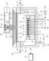
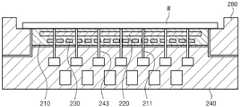
参考图1,基板处理装置在基板W上执行等离子体工艺。基板处理装置包括工艺腔室100、基板支承构件200、气体供应构件300、微波施用单元400和控制器500。Referring to FIG. 1 , a substrate processing apparatus performs a plasma process on a substrate W. As shown in FIG. The substrate processing apparatus includes a
工艺腔室100可以具有反应空间101。反应空间101可以为在其中处理基板的空间。开口(未示出)可以形成在工艺腔室100的侧壁上。开口设置成通路,基板W可以通过该通路进入或退出工艺腔室100。开口由门(未示出)打开或关闭。排放孔102形成在工艺腔室100的底表面上。排放孔102连接至排放管线121。排放管线121可以连接至减压构件123。减压构件123可以为泵。工艺期间产生的反应副产物和残余在工艺腔室100内部的气体可以通过排放管线121排出到外部。The
此外,反应空间101的压力可以通过由减压构件123经由排放管线121提供的减压而维持在设定压力。反应空间101的压力可以维持在接近于真空的压力。也就是说,工艺腔室100可以为真空腔室,在该真空腔室中、在处理基板W期间,反应空间101的压力维持在接近于真空的压力。例如,后面将描述的控制器500可以控制减压构件123使得反应空间101的压力变为10mTorr与4Torr之间的压力(例如10mTorr以上,且4Torr以下)。Furthermore, the pressure of the
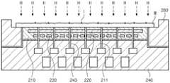
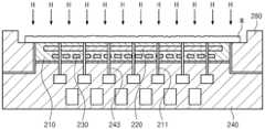
基板支承构件200位于工艺腔室100内部。基板支承构件200支承基板W。基板支承构件200可以包括静电卡盘ESC,该静电卡盘210使用静电力吸附基板W。The substrate support member 200 is located inside the
描述了根据实施方案的基板支承构件200包括静电卡盘ESC。基板支承构件200包括介电板210、底部电极220、加热器230、支承板240、绝缘板270和聚焦环280。The substrate support member 200 according to the embodiment is described to include an electrostatic chuck ESC. The substrate support member 200 includes a
介电板210位于基板支承构件200的顶端处。介电板210设置成盘状的介电质。基板W设置在介电板210的顶表面上。介电板210的顶表面的半径小于基板W的半径。因此,基板W的边缘区域可以位于介电板210的外部。第一供应流体通道211形成在介电板210处。第一供应流体通道211设置为从介电板210的顶表面到介电板210的底表面。多个第一供应流体通道211形成为彼此间隔开来,并且设置成为通路,传热介质通过该通路供应至基板W的底表面。The
底部电极220和加热器230埋入到介电板210内。底部电极220位于加热器230的上方。底部电极220电连接至底部电源221。底部电源221包括直流电源。底部电源开关222安装在底部电极220和底部电源221之间。底部电极220可以通过底部电源开关222的打开/关闭而电连接至底部电源221。当底部电源开关222打开时,直流电流施用到底部电极220。电力通过施用到底部电极220的电流而作用到底部电极220和基板W之间,且基板W通过该电力而吸附至介电板210。The
加热器230可以为将基板W的温度调节至设定温度的温度控制构件。此外,基板W通过由加热器230产生的热量而维持在设定温度。加热器230包括具有螺旋形状的线圈。加热器230可以以均匀的间隔而埋入在介电板210中。加热器230可以通过接收来自加热器电源231功率而进行加热。此外,加热器电源开关232可以安装在加热器230和加热器电源231之间。加热器230可以通过打开/关闭加热器电源开关232而电连接至加热器电源231。此外,加热器230的温度可以根据由加热器电源231施加到加热器的功率量级而改变。例如,加热器230的温度还可以与施用到加热器230的功率量级成比例地增加。此外,加热器230可以连接至加热器传感器(未示出),该加热器传感器感应加热器230的温度。加热器传感器可以实时感应加热器230的温度,并将检测到的加热器230的实时温度传输至后面将描述的控制器500。控制器500可以基于由加热器传感器感应到的加热器230的温度而改变传输至加热器230的功率量级。The
支承板240位于介电板210下方。介电板210的底表面和支承板240的顶表面可以通过胶粘剂236粘附。支承板240可以设置成铝材。支承板240的顶表面可以为阶梯式的,使得中心区域定位成高于边缘区域。支承板240的顶表面的中心区域具有对应于介电板210的底表面的面积,并粘附至介电板210的底表面。第一循环流体通道241、第二循环流体通道242和第二供应流体通道243形成在支承板240处。The
第一循环流体通道241设置成传热介质通过其循环的通路。第一循环流体通道241可以在支承板240中形成为螺旋形状。可替代地,第一循环流体通道241可以设置成使得具有不同半径的环形流体通道具有相同的中心。第一循环流体通道241中的每个可以彼此连通。第一循环流体通道241形成在相同高度处。The first circulating
第二循环流体通道242设置成冷却流体通过其循环的通路。第二循环流体通道242可以在支承板240内形成为螺旋形状。可替代地,第二循环流体通道242可以设置成使得具有不同半径的环形流体通道具有相同的中心。第二循环流体通道242中的每个可以彼此连通。第二循环流体通道242的截面积大于第一循环流体通道241的截面积。第二循环流体通道242形成在相同高度处。第二循环流体通道242可以位于第一循环流体通道241的下方。The second circulating
第二供应流体通道243从第一循环流体通道241向上延伸并可以设置到支承板240的顶表面。第二供应流体通道243在数量上可以设置成对应于第一供应流体通道211,并连接第一循环流体通道241和第一供应流体通道211。The second
第一循环流体通道241通过传热介质供应管线251连接至传热介质存储单元252。传热介质存储在传热介质存储单元252中。传热介质包括惰性气体。根据实施方案,传热介质包括氦(He)气。氦气通过供应管线251供应到第一循环流体通道241,并可以依序通过第二供应流体通道243和第一供应流体通道211供应到基板W的底表面。氦气用作介质,从等离子体传递至基板W的热量通过该介质传送至基板支承构件200。包含在等离子体中的离子粒子被基板支承构件200中形成的电力吸引,并移动到基板支承构件200,并在移动时与基板W碰撞以执行刻蚀工艺。在离子粒子与基板W碰撞时在基板W处产生热量。从基板W产生的热量通过供应到基板W的底表面和介电板210的顶表面之间空间的氦气而传送至基板支承构件200。因此,基板W可以维持在设定温度。The first circulating
第二循环流体通道242通过冷却流体供应管线261而连接至冷却流体存储单元262。冷却流体存储在冷却流体存储单元262中。冷却器263可以设置在冷却流体存储单元262内。冷却器263可以将冷却流体冷却至预设温度。可替代地,冷却器263可以安装在冷却流体供应管线261上。通过冷却流体供应管线261供应至第二循环流体通道242的冷却流体沿着第二循环流体通道242循环以冷却支承板240。支承板240的冷却将介电板210和基板W一同冷却以将基板W维持在预设温度。The second circulating
绝缘板270设置在支承板240下方。绝缘板270在尺寸上设置成对应于支承板240的尺寸。绝缘板270位于支承板240和腔室100的底表面之间。绝缘板270由绝缘材料制成,并将支承板240与腔室100电绝缘。The insulating
聚焦环280设置在基板支承构件200的边缘区域中。聚焦环280具有环形形状并沿着介电板210的圆周设置。聚焦环280的顶表面可以为阶梯式的,使得外部280a高于内部280b。聚焦环280的顶表面的内部280b位于与介电板210的顶表面相同的高度处。聚焦环280的顶表面的内部280b支承位于介电板210外部的基板W的边缘区域。聚焦环280的外部280a设置成围绕基板W的边缘区域。聚焦环280扩大了电场形成区域,使得基板W位于形成等离子体的区域的中心处。因此,等离子体在基板W的整个区域上方均匀地形成,使得基板W的每个区域可以被均匀地刻蚀。The
气体供应构件300将气体供应至工艺腔室100的反应空间101。气体供应构件300可以通过形成在工艺腔室100的侧壁中的第一气体供应孔105和第二气体供应孔108将气体供应到工艺腔室100中。通过气体供应构件300供应至反应空间101的气体包括工艺气体和钝化气体。工艺气体可以包括选自以下的至少一种气体:氢气、惰性气体或它们的组合。惰性气体的示例可以包括氦气(He)、氖气(Ne)、氩气(Ar)、氪气(Kr)、氙气(Xe)和氡气(Rn)等。钝化气体可以包括选自以下的至少一种气体:氮系气体、惰性气体或它们的组合。例如,氮系气体可以包括选自以下的至少一种气体:N2、氨气(NH3)、联氨(NH4)或它们的组合。惰性气体的示例可以包括氦气(He)、氖气(Ne)、氩气(Ar)、氪气(Kr)、氙气(Xe)和氡气(Rn)等。The
第一气体供应孔105连接至第一气体供应管线310。第一气体供应管线310连接至工艺气体供应源(未示出)。打开/关闭构件311安装在第一气体供应管线310处,并且可以根据该打开/关闭构件311的打开/关闭操作来控制是否将工艺气体供应至反应空间101。第二气体供应孔108连接至第二气体供应管线320。第二气体供应管线320连接至钝化气体供应源(未示出)。打开/关闭构件321安装在第二气体供应管线320处,并且可以根据该打开/关闭构件321的打开/关闭操作来控制是否将钝化气体供应至反应空间101。The first
微波施用单元400设置成为等离子体源的示例,该等离子体源将能量施用至工艺腔室100的反应空间101,以将反应空间101中的气体激发成为等离子体。微波施用单元400可以通过激发工艺气体和/或钝化气体而产生等离子体。The
从工艺气体激发的等离子体包括氢基团。可以将氢基团施用至基板W以去除附接至基板W的杂质,或改善关于基板W的表面的粗糙度。从钝化气体激发的等离子体钝化绝缘组件的表面。绝缘组件可以例如为设置成反应空间101的顶棚(ceiling)的圆顶构件490、侧壁衬里(未示出)、排放隔板(未示出)等。这些组件的至少一个可以例如由诸如石英、Al2O3、AlN、Y2O3的材料制成。The plasma excited from the process gas includes hydrogen radicals. Hydrogen groups may be applied to the substrate W to remove impurities attached to the substrate W or to improve roughness with respect to the surface of the substrate W. The plasma excited from the passivation gas passivates the surface of the insulating component. The insulating components may be, for example,
微波施用单元400包括微波电源410、波导420、微波天线430、介电板470、冷却板480和圆顶构件490。The
微波电源410产生微波。波导420连接至微波电源410,并提供从微波电源410产生的微波通过其进行传送的通路。The
微波天线430位于波导420的前端内部。微波天线430将通过波导420传送的微波施用至工艺腔室100的内部。例如,微波天线430可以接收由微波电源410施用的功率并将微波施用至反应空间101。在实施方案中,微波可以具有频率为2.45GHz的预设功率。施用至微波电源410的功率可以在从约1000W至约3500W的范围内。The
微波天线430包括天线板431、天线杆433、外部导体434、微波适配器436、连接器441、冷却板443和天线高度调节单元445。The
天线板431设置成薄盘,并且形成有多个槽孔432。槽孔432提供微波通过其穿过槽孔432的通路。槽孔432可以设置成各种形状。槽孔432可以设置成诸如“×”、“+”或“-”等的形状。槽孔432可以布置成限定多个环形状。环可以具有相同的中心并具有不同尺寸的半径。The
天线杆433设置成圆柱形杆。天线杆433以其纵向方向在上/下的方式进行设置。天线杆433位于天线板431的上方,天线杆的底端部插入并固定至天线板431的中心。天线杆433将微波传播至天线板431。The
外部导体434位于波导420的前端下方。连接至波导420的内部空间的空间在上/下方向上形成在外部导体434内。天线杆433的部分区域位于外部导体434内。The
微波适配器436位于波导420的前端部内。微波适配器436具有圆锥形状,在该圆锥形状中顶端具有比底端更大的半径。具有敞开的底表面的容纳空间形成在微波适配器436的底端处。
连接器441位于容纳空间处。连接器441设置成环形状。连接器441的外面的半径对应于容纳空间的内面。连接器441的外面通过与容纳空间的内面接触而固定定位。连接器441可以由导电材料形成。天线杆433的顶端位于容纳空间内并适配到连接器441的内部区域中。天线杆433的顶端按压适配到连接器441中,并且通过该连接器441电连接至微波适配器436。The
冷却板443耦接至微波适配器436的顶端。冷却板443可以设置成为具有比微波适配器436的顶端部更大的半径的板。冷却板443可以由具有比微波适配器436更好的热导率的材料制成。冷却板443可以由铜(Cu)或铝(Al)制成。冷却板433促进微波适配器436的冷却,进而防止微波适配器436的热形变。The
天线高度调节单元445连接微波适配器436和天线杆433。此外,天线高度调节单元445移动天线杆433从而改变天线板431相对于微波适配器436的相对高度。天线高度调节单元445包括螺栓。螺栓445从微波适配器436的顶部到微波适配器436底部沿上/下方向插入到微波适配器436中,并且底端位于容纳空间中。螺栓445插入到微波适配器436的中心区域。螺栓445的底端插入到天线杆433的顶端。在天线杆433的顶端部的预设深度处形成有螺纹槽,螺栓445的底端插入并紧固到该螺纹槽中。天线杆433根据螺栓445的旋转而在上/下方向上移动。例如,当螺栓445顺时针旋转时,天线杆433可以升高,并且当螺栓445逆时针旋转时,天线杆433可以下降。天线板431可以与天线杆433的移动在上/下方向上一同移动。The antenna
介电板470位于天线板431上方。介电板470设置成介电材料,诸如氧化铝或石英。从微波天线430在上/下方向上传播的微波在介电板470的径向上传播。传播至介电板470的微波被压缩并共振。共振微波被传输到天线板431的槽孔432。The
冷却板480设置在介电板470上方。冷却板480冷却介电板470。冷却板480可以由铝材形成。冷却板480可以通过使冷却流体流过形成在其中的冷却流体通道(未示出)来冷却介电板470。冷却方法包括水冷法和气冷法。The
圆顶构件490设置在天线板431下方。圆顶构件490设置成介电材料,诸如氧化铝或石英。穿过天线板431的槽孔432的微波通过圆顶构件490辐射到工艺腔室100中。通过发射的微波的电场而供应到工艺腔室100中的工艺气体在等离子体状态下被激发成。圆顶构件490的顶表面可以与天线板431的底表面间隔开预设间隔。The
天线高度调节单元445可以在上/下方向上移动天线杆433从而改变天线板431相对于微波适配器436的相对高度。天线高度调节单元445可以在上/下方向上移动天线杆433,以适当间隔保持天线板431和圆顶构件490。The antenna
控制器500可以控制基板处理装置。控制器500可以控制基板处理装置的减压构件123、基板支承构件200、气体供应构件300和微波施用单元400的至少一种,以执行以下描述的基板处理方法。此外,控制器500可以设置有:工艺控制器,该工艺控制器由控制基板处理装置的微处理器(计算机)制成;键盘,操作员在键盘中操作指令输入操作等以管理基板处理装置;用户界面,该用户界面由可视化并展示基板处理装置的操作的显示器或其他物体制成;控制程序,用于在工艺控制器的控制下在基板处理装置中执行处理;程序,用于根据各种数据和处理条件在每个组件中执行处理;以及存储单元,该存储单元存储处理配方(recipe)。此外,用户界面和存储单元可以连接至工艺控制器。处理配方可以存储在存储单元的存储介质中,该存储介质可以为硬盘、可移动磁盘(诸如CD-ROM、DVD),或半导体存储器(诸如闪存)。The
控制器500可以通过调节由加热器电源231传送至加热器230的功率量级而将基板W的温度维持在设定温度。例如,控制器500可以识别由加热器传感器实时检测的加热器230的温度。此外,可以将基板W的温度根据加热器230的温度而改变的参数输入到控制器500中,加热器230的温度是预先执行的实验数据。控制器500可以控制工艺气体和钝化气体的供应。控制器500可以控制减压构件123以调节反应空间101的压力。The
图2为示出了根据本发明构思的实施方案的基板处理方法的流程图。参考图2,根据本发明构思的实施方案的基板处理方法依序执行步骤S10、S20、S30、S40和S50。根据本发明构思的另一实施方式,步骤S10和S20可以依序执行,且步骤S30、S40和S50可以在步骤S20之后同时执行。可替代地,根据本发明构思的另一实施方式,在步骤S10之后,可以同时或依序执行步骤S20和步骤S40,并在步骤S30之后执行步骤S50。根据本发明构思的实施方案的基板处理方法同时执行钝化步骤和等离子体退火步骤。因此,能够缩短等离子体退火前执行钝化所需的时间,从而缩短工艺进程时间。FIG. 2 is a flowchart illustrating a substrate processing method according to an embodiment of the present inventive concept. Referring to FIG. 2 , the substrate processing method according to an embodiment of the present inventive concept sequentially performs steps S10 , S20 , S30 , S40 and S50 . According to another embodiment of the present inventive concept, steps S10 and S20 may be performed sequentially, and steps S30, S40 and S50 may be performed simultaneously after step S20. Alternatively, according to another embodiment of the present inventive concept, after step S10, step S20 and step S40 may be performed simultaneously or sequentially, and step S50 may be performed after step S30. The substrate processing method according to an embodiment of the present inventive concept simultaneously performs the passivation step and the plasma annealing step. Therefore, the time required to perform passivation before plasma annealing can be shortened, thereby shortening the process time.
带入反应空间中的基板W可以由包括硅(Si)的材料制成。The substrate W brought into the reaction space may be made of a material including silicon (Si).
根据本发明构思的实施方式的基板处理方法,将基板W引入到反应空间101中(步骤S10)。作为钝化气体的示例,将氮系气体供应至反应空间101,在该反应空间101内已经设置有基板(步骤S20)。可以在50mTorr至1Torr的压力气氛中以10sccm至1000sccm的流速供应氮系气体10秒至60秒。当氮系气体充分供应到反应空间101时,停止氮系气体的供应(S30)。According to the substrate processing method of the embodiment of the present inventive concept, the substrate W is introduced into the reaction space 101 (step S10 ). As an example of the passivation gas, a nitrogen-based gas is supplied to the
将工艺气体供应至反应空间101,在该反应空间101内已经设置有基板W(步骤S40)。例如,工艺气体为氢气、惰性气体或它们的组合。在氮系气体保留在反应空间101中的状态下引入工艺气体。将工艺气体引入到反应空间101中,并在氮系气体保留在反应空间101中的情况下将反应空间101中的气体激发成等离子体(步骤S50)。在实施方案中,将微波电源410控制为打开状态,并因此将反应空间101中的工艺气体和氮系气体激发成等离子体状态。The process gas is supplied to the
根据步骤S10至S50,在已经将基板W引入到反应空间的状态下将氮系气体供应至反应空间之后,在供应工艺气体但停止供应氮系气体的情况下执行等离子体生成步骤,从而在等离子体生成步骤中、可以同时执行使用保留的氮基的钝化以及氢等离子体退火。According to steps S10 to S50, after the nitrogen-based gas is supplied to the reaction space in a state where the substrate W has been introduced into the reaction space, the plasma generation step is performed with the supply of the process gas but the supply of the nitrogen-based gas is stopped, so that the plasma In the bulk generation step, passivation using the remaining nitrogen groups and hydrogen plasma annealing may be performed simultaneously.
图3为示出了根据本发明构思实施方案执行图2的步骤S20的基板处理装置状态的视图。除了图2以外进一步参考图3,将描述在执行步骤S20的状态下的基板处理装置。参考图3,打开第二气体供应管线320的打开/关闭构件321以将氮系气体引入到反应空间101中。在此情况下,微波电源410控制在关闭状态。FIG. 3 is a view illustrating a state of the substrate processing apparatus performing step S20 of FIG. 2 according to an embodiment of the present inventive concept. With further reference to FIG. 3 in addition to FIG. 2 , the substrate processing apparatus in a state where step S20 is performed will be described. Referring to FIG. 3 , the opening/closing
图4为示出了根据本发明构思实施方案执行图2的步骤S40和S50的基板处理装置状态的视图。除了图2以外进一步参考图4,将描述在执行步骤S40和S50的状态下的基板处理装置。参考图4,打开第一气体供应管线310的打开/关闭构件311以将工艺气体引入到反应空间101中。根据工艺气体的引入,工艺气体在基板W周围流动,并且氮系气体保留在基板W外周之外的区域中。在此情况下,微波电源410控制为打开。由于微波电源410控制为打开,因此引入的工艺气体和保留的氮系气体被激发成等离子体状态。FIG. 4 is a view illustrating a state of the substrate processing apparatus performing steps S40 and S50 of FIG. 2 according to an embodiment of the present inventive concept. With further reference to FIG. 4 in addition to FIG. 2 , the substrate processing apparatus in a state where steps S40 and S50 are performed will be described. Referring to FIG. 4 , the opening/closing
图5为示意性显示了由通过图2的步骤S50的氮钝化而改变绝缘组件的表面的视图。尽管图5示出了材料为石英(SiO2)的情况,但是本领域的技术人员将理解的是,同样可以应用其他绝缘材料(例如Al2O3、AlN、Y2O3)。FIG. 5 is a view schematically showing that the surface of the insulating member is changed by nitrogen passivation through step S50 of FIG. 2 . Although FIG. 5 shows the case where the material is quartz (SiO2 ), those skilled in the art will understand that other insulating materials (eg, Al2 O3 , AlN, Y2 O3 ) can be applied as well.
参考图5,可以看出,石英部件表面的一部分转化为氧氮化硅(SiON)。也就是说,SiON并未作为新层而沉积在先前的石英表面上,而是先前的石英表面通过钝化转化为具有预设厚度的SiON。本文中,氮(N)可以来源于用于钝化的氮系气体,且其他元素(即硅(Si)和氧(O))可以来源于石英。Referring to Figure 5, it can be seen that a portion of the surface of the quartz component is converted to silicon oxynitride (SiON). That is, SiON is not deposited as a new layer on the previous quartz surface, but the previous quartz surface is converted to SiON with a preset thickness by passivation. Herein, nitrogen (N) may be derived from a nitrogen-based gas for passivation, and other elements, ie, silicon (Si) and oxygen (O), may be derived from quartz.
图6为示出了在执行图2的步骤S50的工艺中第一处理步骤中基板状态的视图。图7为示出了在执行图2的步骤S50的工艺中第二处理步骤中基板状态的视图。第一处理步骤和第二处理步骤为在基板上执行氢等离子体退火(HPA)的步骤的实施例。FIG. 6 is a view showing the state of the substrate in the first processing step in the process of performing step S50 of FIG. 2 . FIG. 7 is a view showing the state of the substrate in the second processing step in the process of performing step S50 of FIG. 2 . The first processing step and the second processing step are examples of steps of performing hydrogen plasma annealing (HPA) on the substrate.
参考图6,第一处理步骤可以为去除残留在基板W上的杂质I的步骤。在第一处理步骤中待去除的杂质I可以是在刻蚀基板时产生的刻蚀副产物和刻蚀工艺之后残留的残余膜(未刻蚀的一部分膜)。例如,附接至基板W的杂质I可以为包含锗(Ge)的化合物。例如,杂质I可以包括SiGe或GeO。Referring to FIG. 6 , the first processing step may be a step of removing impurities I remaining on the substrate W. As shown in FIG. The impurity I to be removed in the first processing step may be etching by-products generated when the substrate is etched and a residual film (a part of the film that is not etched) remaining after the etching process. For example, the impurity I attached to the substrate W may be a compound including germanium (Ge). For example, the impurity I may include SiGe or GeO.
在第一处理步骤中,控制器500可以控制基板支承构件200将基板W的温度维持在第一温度。第一温度可以在50与300摄氏度之间(例如大于等于50摄氏度,且小于等于300摄氏度)。更具体地,第一温度可以在160摄氏度与200摄氏度之间。此外,当从工艺气体激发的氢基团传送至基板W的表面时,基板W的温度可以维持在第一温度以去除残留在基板W上的杂质I。硅(Si)和锗(Ge)与氢基团反应且变为挥发性物质,并且它们可以从基板W的表面去除。In the first processing step, the
如图7所示,当完成第一处理步骤S10的执行时,可以从基板W去除附接至基板W的杂质I。As shown in FIG. 7 , when the execution of the first processing step S10 is completed, the impurities I attached to the substrate W may be removed from the substrate W. As shown in FIG.
图8为示出了在执行图2的步骤S50的工艺中第二处理步骤中基板状态的视图。参考图8,第二处理步骤可以为改善基板W的表面粗糙度的步骤。如上所述,基板W可以由包括硅(Si)的材料制成。FIG. 8 is a view showing the state of the substrate in the second processing step in the process of performing step S50 of FIG. 2 . Referring to FIG. 8 , the second processing step may be a step of improving the surface roughness of the substrate W. As shown in FIG. As described above, the substrate W may be made of a material including silicon (Si).
在第二处理步骤中,控制器500可以控制基板支承构件200将基板W的温度维持在与上述第一温度不同的第二温度。第二温度可以高于第一温度。第二温度可以为400℃与700℃之间的温度(例如400℃以上,且700℃以下)。此外,当从工艺气体激发的氢基团传送至基板W的表面时,基板W的温度从第一温度变化至第二温度,并维持在第二温度,从而改善基板W的粗糙度。In the second processing step, the
如图9所示,当完成第二处理步骤的执行时,可以改善基板W的表面粗糙度。As shown in FIG. 9 , when the execution of the second processing step is completed, the surface roughness of the substrate W can be improved.
在执行第一处理步骤之后执行第二处理步骤。由于在已经从基板W去除杂质的状态下执行第二处理步骤,因此可以最小化半导体设备性能劣化的问题。The second processing step is performed after performing the first processing step. Since the second processing step is performed in a state where impurities have been removed from the substrate W, the problem of performance degradation of the semiconductor device can be minimized.
第一温度和第二温度可以根据硅(Si)和锗(Ge)变为挥发性物质(SiH4和GeH4)的主要温度范围进行分类。当硅(Si)和锗(Ge)与氢基团反应变为挥发性物质时,它们可以从基板W的表面去除。The first temperature and the second temperature can be classified according to the main temperature range in which silicon (Si) and germanium (Ge) become volatile substances (SiH4 and GeH4 ). When silicon (Si) and germanium (Ge) react with hydrogen groups to become volatile substances, they may be removed from the surface of the substrate W.
锗(Ge)被氢基团去除的温度范围可以是50摄氏度至300摄氏度。在实施方案中,通过氢基团的锗(Ge)去除效率最高的温度为约180摄氏度。在第一处理步骤中,优选基板W的温度不超过300摄氏度。这是因为当温度超过300摄氏度时,可能会去除基板的硅。在硅(Si)基板的情况下,通过氢基团去除硅的温度范围为约300℃至400℃,并因此当第一处理步骤S10中基板W的温度超过300℃时,不仅包括锗(Ge)的杂质可以被去除,硅也可能被去除,而损伤基板W。The temperature at which germanium (Ge) is removed by hydrogen groups may range from 50 degrees Celsius to 300 degrees Celsius. In embodiments, the temperature at which germanium (Ge) removal by hydrogen groups is most efficient is about 180 degrees Celsius. In the first processing step, it is preferable that the temperature of the substrate W does not exceed 300 degrees Celsius. This is because the silicon of the substrate may be removed when the temperature exceeds 300 degrees Celsius. In the case of a silicon (Si) substrate, the temperature for removing silicon by hydrogen groups ranges from about 300°C to 400°C, and thus when the temperature of the substrate W in the first processing step S10 exceeds 300°C, not only germanium (Ge ) impurities may be removed, and silicon may also be removed, thereby damaging the substrate W.
在第二处理步骤中,如上所述优选基板W的温度维持在400摄氏度至700摄氏度。在硅(Si)的情况下,在氢基团气氛中当基板W的温度维持在约400℃至700℃时,硅(Si)具有表面扩散作用,从而改善基板W的表面粗糙度。在第二处理步骤中,优选基板W的温度超过400℃。在在基板W中包括硅(Si)的情况下,由氢基团去除硅的温度范围为约300℃至400℃,并且在第二步骤中当基板W的温度下降到低于400℃时,可能无法改善基板W的表面粗糙度,但可能会发生对基板W自身的损伤。In the second processing step, the temperature of the substrate W is preferably maintained at 400 degrees Celsius to 700 degrees Celsius as described above. In the case of silicon (Si), when the temperature of the substrate W is maintained at about 400°C to 700°C in a hydrogen group atmosphere, the silicon (Si) has a surface diffusion effect, thereby improving the surface roughness of the substrate W. In the second processing step, it is preferable that the temperature of the substrate W exceeds 400°C. In the case where silicon (Si) is included in the substrate W, the temperature at which silicon is removed by hydrogen groups ranges from about 300°C to 400°C, and when the temperature of the substrate W drops below 400°C in the second step, The surface roughness of the substrate W may not be improved, but damage to the substrate W itself may occur.
图10为示出了根据本发明构思另一实施方式同时执行图2的步骤S20和S40的基板处理装置状态的视图。图11为示出了根据本发明构另一思实施方式执行图2的步骤S40和S50的基板处理装置状态的视图。除了图2以外将依序参照图10和图11来描述根据本发明构思的另一实施方式的基板处理方法。FIG. 10 is a view illustrating a state of a substrate processing apparatus in which steps S20 and S40 of FIG. 2 are simultaneously performed according to another embodiment of the present inventive concept. FIG. 11 is a view illustrating a state of a substrate processing apparatus performing steps S40 and S50 of FIG. 2 according to another embodiment of the present invention. A substrate processing method according to another embodiment of the present inventive concept will be described with reference to FIGS. 10 and 11 in sequence in addition to FIG. 2 .
参考图10,在根据本发明构思的步骤S20引入氮系气体中,可以一同供应步骤S40的工艺气体。即使一同执行步骤S20和S40,也要在执行步骤S50之前执行步骤S30。Referring to FIG. 10 , in the nitrogen-based gas introduced in step S20 according to the present inventive concept, the process gas of step S40 may be supplied together. Even if steps S20 and S40 are performed together, step S30 is performed before step S50 is performed.
根据本发明构思的基板处理方法的另一实施方式,将基板W引入到反应空间101中(步骤S10)。在将基板W带入反应空间101之后,氮系气体作为钝化气体的示例被供应至反应空间101(步骤S20)。可以在50mTorr至1Torr的压力气氛下以10sccm至1000sccm的流速供应氮系气体10秒至60秒。在供应氮系气体的情况下,将工艺气体供应至反应空间101(步骤S40)。可以在50mTorr至1Torr的压力气氛下以10sccm至1000sccm的流速供应工艺气体10秒至60秒。According to another embodiment of the substrate processing method of the present inventive concept, the substrate W is introduced into the reaction space 101 (step S10). After the substrate W is brought into the
参考图11,当氮系气体充分供应到反应空间101时,停止氮系气体的供应(S30)。将工艺气体引入到反应空间101中,并在氮系气体保留在反应空间101中的情况下将反应空间101中的气体激发成等离子体(步骤S50)。在实施方案中,在反应空间101中,将微波电源410控制为打开状态,并因此将反应空间101中的工艺气体和氮系气体激发成等离子体状态。Referring to FIG. 11, when the nitrogen-based gas is sufficiently supplied to the
根据步骤S10至S50,在已经将基板引入到反应空间的状态下将氮系气体供应至反应空间之后,在供应工艺气体但停止供应氮系气体的情况下执行等离子体生成步骤,从而可以在等离子体生成步骤中同时执行使用保留的氮系气体的钝化以及氢等离子体退火。According to steps S10 to S50, after the nitrogen-based gas is supplied to the reaction space in a state where the substrate has been introduced into the reaction space, the plasma generation step is performed with the process gas supplied but the supply of the nitrogen-based gas is stopped, so that the plasma Passivation using the remaining nitrogen-based gas and hydrogen plasma annealing are simultaneously performed in the bulk generation step.
当在基板W上执行氢等离子体退火时,在基板W的表面具有SiON钝化层的组件可以转化为SiO2。换句话说,当在对表面上具有SiON钝化层的组件上执行氢等离子体退火(hydrogen plasma annealing,HPA)时,SiON可以转化为预钝化状态,即SiO2。根据本发明构思的实施方案,在供应氮系气体之后,引入工艺气体,并从其中激发等离子体。因此,在使用保留在反应空间101中的氮气对绝缘组件进行氮钝化的同时执行氢等离子体退火工艺。因此,缩短了整个工艺时间,并且可以在维持绝缘作用件的氮钝化表面的同时执行氢等离子体退火工艺。When hydrogen plasma annealing is performed on the substrate W, the component having the SiON passivation layer on the surface of the substrate W may be converted into SiO2 . In other words, when hydrogen plasma annealing (HPA) is performed on a component having a passivation layer of SiON on the surface, SiON can be converted into a pre-passivated state, ie, SiO2 . According to an embodiment of the present inventive concept, after the nitrogen-based gas is supplied, a process gas is introduced, and plasma is excited therefrom. Therefore, the hydrogen plasma annealing process is performed while the insulating components are nitrogen passivated using the nitrogen gas remaining in the
然而,当通过消耗SiON层中的大部分氮而将SiON转化为SiO2时,SiO2中的氧可能会与氢基团反应并分离成OH*形式。这意味着对石英组件的损坏,因为这导致了SiO2中的氧损失。然而,根据本发明构思的实施方案,通过与氢等离子体退火工艺同时执行钝化、在缩短整体工艺时间的情况下,可以防止对石英组件的损坏。例如,根据本发明构思的实施方案,与现有技术相比,每设备小时单位(unit per equipment hour,UPEH)可提高1.5倍。However, when SiON is converted to SiO by consuming most of the nitrogen in theSiON layer, the oxygen in SiO may react withhydrogen groups and separate into OH* forms. This means damage to the quartz components as this leads to loss of oxygen in theSiO2 . However, according to an embodiment of the present inventive concept, by performing passivation simultaneously with the hydrogen plasma annealing process, damage to the quartz component may be prevented while reducing the overall process time. For example, according to an embodiment of the present inventive concept, the unit per equipment hour (UPEH) may be improved by a factor of 1.5 compared to the prior art.
如上所述,可以将在其上完成氢等离子体退火处理的基板W从反应空间101中载出。例如可以通过诸如机械臂的装置将基板W载出。As described above, the substrate W on which the hydrogen plasma annealing treatment is completed can be carried out from the
在将基板W取出后,将待处理的基板带入到反应空间101中,并可以执行步骤S20至S50。同时,在根据需要和实验结果对一个基板执行步骤S10至S50之后,可以对接下来待处理的n个基板的一些仅执行步骤S50。可以将n块适当地调节至在钝化的绝缘构件的表面失去钝化效果之前的时间点。After the substrate W is taken out, the substrate to be processed is brought into the
在上述实施例中,通过微波生成包括氢基团的等离子体,但本发明构思不限于此,并且可以等同地或类似地施用上述实施方案,只要具有用于控制基板W的温度的温度控制构件和用于从工艺气体生成等离子体的等离子体源即可。In the above-described embodiments, plasma including hydrogen groups is generated by microwaves, but the present inventive concept is not limited thereto, and the above-described embodiments may be equally or similarly applied as long as there is a temperature control member for controlling the temperature of the substrate W and a plasma source for generating plasma from the process gas.
发明构思效果不限于以上提及的效果,并且本发明构思所属领域的技术人员可以从本说明书和附图中清楚的理解未提及的效果。The effects of the inventive concept are not limited to the above-mentioned effects, and those skilled in the art to which the inventive concept pertains can clearly understand the unmentioned effects from the present specification and the accompanying drawings.
到目前为止尽管已经说明并描述了本发明构思的优选实施方案,但本发明构思不限于以上描述的特定实施方案,并且值得注意的是,在不脱离权利要求中请求保护的本发明构思的要素的情况下,从属于本发明构思领域的普通技术人员可以不同的执行本发明构思,并且修改不应与发明构思的技术精神或前景分开解释。While preferred embodiments of the inventive concept have been illustrated and described thus far, the inventive concept is not limited to the particular embodiments described above, and it is worth noting that there is no departure from the elements of the inventive concept claimed in the claims. In this case, those of ordinary skill in the field of the inventive concept may perform the inventive concept differently, and the modifications should not be interpreted separately from the technical spirit or prospect of the inventive concept.
Claims (20)
Translated fromChineseApplications Claiming Priority (2)
| Application Number | Priority Date | Filing Date | Title |
|---|---|---|---|
| KR1020200188108AKR102614922B1 (en) | 2020-12-30 | 2020-12-30 | Apparatus and method for treating substrate |
| KR10-2020-0188108 | 2020-12-30 |
Publications (2)
| Publication Number | Publication Date |
|---|---|
| CN114695059Atrue CN114695059A (en) | 2022-07-01 |
| CN114695059B CN114695059B (en) | 2025-10-14 |
Family
ID=
Citations (5)
| Publication number | Priority date | Publication date | Assignee | Title |
|---|---|---|---|---|
| US20060046355A1 (en)* | 2004-08-24 | 2006-03-02 | Parekh Kunal R | Methods of forming semiconductor constructions |
| CN103426818A (en)* | 2013-08-05 | 2013-12-04 | 上海华力微电子有限公司 | Method for repairing plasma damage in metal interconnection layer process |
| US20170162369A1 (en)* | 2015-12-04 | 2017-06-08 | Samsung Electronics Co., Ltd. | Method for preparing hydrogen plasma annealing treatment, method for performing hydrogen plasma annealing treatment, and apparatus therefor |
| CN108630513A (en)* | 2017-03-23 | 2018-10-09 | 株式会社日立高新技术 | Plasma processing apparatus and method of plasma processing |
| US20190326115A1 (en)* | 2014-09-15 | 2019-10-24 | Applied Materials, Inc. | Pre-clean of silicon germanium for pre-metal contact at source and drain and pre-high k at channel |
Patent Citations (6)
| Publication number | Priority date | Publication date | Assignee | Title |
|---|---|---|---|---|
| US20060046355A1 (en)* | 2004-08-24 | 2006-03-02 | Parekh Kunal R | Methods of forming semiconductor constructions |
| CN103426818A (en)* | 2013-08-05 | 2013-12-04 | 上海华力微电子有限公司 | Method for repairing plasma damage in metal interconnection layer process |
| US20190326115A1 (en)* | 2014-09-15 | 2019-10-24 | Applied Materials, Inc. | Pre-clean of silicon germanium for pre-metal contact at source and drain and pre-high k at channel |
| US20170162369A1 (en)* | 2015-12-04 | 2017-06-08 | Samsung Electronics Co., Ltd. | Method for preparing hydrogen plasma annealing treatment, method for performing hydrogen plasma annealing treatment, and apparatus therefor |
| CN108630513A (en)* | 2017-03-23 | 2018-10-09 | 株式会社日立高新技术 | Plasma processing apparatus and method of plasma processing |
| TWI672742B (en)* | 2017-03-23 | 2019-09-21 | 日商日立全球先端科技股份有限公司 | The plasma processing apparatus and plasma processing method |
Also Published As
| Publication number | Publication date |
|---|---|
| KR20220097679A (en) | 2022-07-08 |
| KR102614922B1 (en) | 2023-12-20 |
| US20220208515A1 (en) | 2022-06-30 |
Similar Documents
| Publication | Publication Date | Title |
|---|---|---|
| US10998204B2 (en) | Method of processing substrate and substrate processing apparatus | |
| KR102143272B1 (en) | Substrate processing apparatus, substrate loading mechanism, and substrate processing method | |
| US20150235860A1 (en) | Etching method and plasma processing apparatus | |
| KR102569911B1 (en) | Focus ring and substrate processing apparatus | |
| TWI587389B (en) | Substrate processing method | |
| CN110735181A (en) | Method and apparatus for pre-cleaning substrate surface prior to epitaxial growth | |
| JPH0831449B2 (en) | Material Removal Equipment Using Confined Plasma Etching | |
| JP2020021958A (en) | Substrate processing apparatus and substrate mounting table | |
| JP2022532775A (en) | Methods and equipment to minimize damage on the back side of the board | |
| JP2019169635A (en) | Cleaning method and processing unit | |
| CN101950721A (en) | Surface treatment method | |
| CN114695059B (en) | Apparatus and method for processing a substrate | |
| CN114695059A (en) | Apparatus and method for processing substrates | |
| US12444576B2 (en) | Apparatus and method for treating substrate | |
| KR102653253B1 (en) | Substrate processing method and substrate processing apparatus | |
| JP3193575B2 (en) | Microwave plasma processing equipment | |
| KR102688353B1 (en) | Apparatus and method for treating substrate | |
| KR102674205B1 (en) | Apparatus and method for treating substrate | |
| TWI837617B (en) | Apparatus and method of treating substrate | |
| JP7593962B2 (en) | SUBSTRATE PROCESSING APPARATUS AND SUBSTRATE PROCESSING METHOD | |
| US20230298860A1 (en) | Apparatus And Method Of Treating Substrate | |
| US20240203697A1 (en) | Apparatus for processing substrate and method of processing substrate | |
| CN116844933A (en) | Apparatus and method for processing substrate | |
| JP7160291B2 (en) | Etching method and etching apparatus | |
| US20230207290A1 (en) | Method of treating substrate |
Legal Events
| Date | Code | Title | Description |
|---|---|---|---|
| PB01 | Publication | ||
| PB01 | Publication | ||
| SE01 | Entry into force of request for substantive examination | ||
| SE01 | Entry into force of request for substantive examination | ||
| GR01 | Patent grant |