CN114695040A - Scanning transmission imaging device in scanning electron microscope - Google Patents
Scanning transmission imaging device in scanning electron microscopeDownload PDFInfo
- Publication number
- CN114695040A CN114695040ACN202210329055.1ACN202210329055ACN114695040ACN 114695040 ACN114695040 ACN 114695040ACN 202210329055 ACN202210329055 ACN 202210329055ACN 114695040 ACN114695040 ACN 114695040A
- Authority
- CN
- China
- Prior art keywords
- sample
- groove
- fixing
- scanning
- electron microscope
- Prior art date
- Legal status (The legal status is an assumption and is not a legal conclusion. Google has not performed a legal analysis and makes no representation as to the accuracy of the status listed.)
- Granted
Links
- 230000005540biological transmissionEffects0.000titleclaimsabstractdescription73
- 238000003384imaging methodMethods0.000titleclaimsabstractdescription39
- 239000000523sampleSubstances0.000claimsabstractdescription189
- 238000003825pressingMethods0.000claimsdescription12
- 239000000463materialSubstances0.000claimsdescription5
- 229910000838Al alloyInorganic materials0.000claimsdescription3
- 238000010894electron beam technologyMethods0.000abstractdescription11
- 238000004458analytical methodMethods0.000abstractdescription5
- 238000004626scanning electron microscopyMethods0.000description12
- 238000001514detection methodMethods0.000description6
- 238000000034methodMethods0.000description6
- 229920000620organic polymerPolymers0.000description3
- 239000007779soft materialSubstances0.000description3
- 238000010586diagramMethods0.000description2
- 238000001493electron microscopyMethods0.000description2
- 239000000203mixtureSubstances0.000description2
- 230000008569processEffects0.000description2
- 238000001350scanning transmission electron microscopyMethods0.000description2
- 230000009286beneficial effectEffects0.000description1
- 238000005516engineering processMethods0.000description1
- 230000006872improvementEffects0.000description1
- 238000009413insulationMethods0.000description1
- 238000012986modificationMethods0.000description1
- 230000004048modificationEffects0.000description1
Images


Classifications
- H—ELECTRICITY
- H01—ELECTRIC ELEMENTS
- H01J—ELECTRIC DISCHARGE TUBES OR DISCHARGE LAMPS
- H01J37/00—Discharge tubes with provision for introducing objects or material to be exposed to the discharge, e.g. for the purpose of examination or processing thereof
- H01J37/26—Electron or ion microscopes; Electron or ion diffraction tubes
- H01J37/28—Electron or ion microscopes; Electron or ion diffraction tubes with scanning beams
- H—ELECTRICITY
- H01—ELECTRIC ELEMENTS
- H01J—ELECTRIC DISCHARGE TUBES OR DISCHARGE LAMPS
- H01J37/00—Discharge tubes with provision for introducing objects or material to be exposed to the discharge, e.g. for the purpose of examination or processing thereof
- H01J37/02—Details
- H01J37/20—Means for supporting or positioning the object or the material; Means for adjusting diaphragms or lenses associated with the support
Landscapes
- Chemical & Material Sciences (AREA)
- Analytical Chemistry (AREA)
- Analysing Materials By The Use Of Radiation (AREA)
Abstract
Description
Translated fromChinese技术领域technical field
本发明公开了一种扫描电镜中的扫描透射成像装置,属于扫描透射电子显微技术领域。The invention discloses a scanning transmission imaging device in a scanning electron microscope, which belongs to the technical field of scanning transmission electron microscopy.
背景技术Background technique
扫描透射电子显微术是利用磁透镜将电子束聚焦到薄样品表面进行扫描,通过收集透射电子信号获取样品内部微观结构信息的一种成像技术,使用该技术制造的扫描透射电子显微镜(Scanning Transmission Electron Microscopy,STEM)已成为表征物质微观结构不可或缺的仪器。STEM是基于高分辨成像需求发展起来的一种电子显微技术,为了得到较高的分辨率,其加速电压一般为200~300kV。由于电子束能量较高,因此不适合观察耐电子束辐照性差的样品。Scanning transmission electron microscopy is an imaging technique that uses a magnetic lens to focus an electron beam on the surface of a thin sample, and obtains information on the internal microstructure of the sample by collecting transmission electron signals. Electron Microscopy, STEM) has become an indispensable instrument for characterizing the microstructure of matter. STEM is an electron microscopy technique developed based on the demand for high-resolution imaging. In order to obtain higher resolution, the accelerating voltage is generally 200-300 kV. Due to the high electron beam energy, it is not suitable for observing samples with poor electron beam resistance.
扫描电子显微镜(Scanning Electron Microscopy,SEM)的加速电压较低,一般不超过30kV,若在SEM中安装STEM装置,可显著减少电子束对样品的损伤,特别适合于有机高分子、生物等软材料样品的透射分析。STEM与SEM的不同之处是STEM使用薄样品,并在样品下方安装一个探测器,当电子束扫描样品某个位置时,探测器将同步接收信号并转换成电流强度显示在电脑屏幕上,样品上的每一点与所产生的像点一一对应。近些年,随着SEM的性能提升及场发射SEM的普及,在SEM上拓展STEM功能的需求也越来越迫切。The accelerating voltage of Scanning Electron Microscopy (SEM) is low, generally not more than 30kV. If a STEM device is installed in the SEM, the damage to the sample by the electron beam can be significantly reduced, and it is especially suitable for soft materials such as organic polymers and biology. Transmission analysis of samples. The difference between STEM and SEM is that STEM uses a thin sample, and a detector is installed under the sample. When the electron beam scans a certain position of the sample, the detector will receive the signal synchronously and convert it into current intensity and display it on the computer screen. Each point on the image corresponds to the generated image point one-to-one. In recent years, with the improvement of SEM performance and the popularization of field emission SEM, the need to expand STEM functions on SEM has become more and more urgent.
在扫描电镜上实现STEM功能的方法通常为将单独制作的STEM附件安装于扫描电镜中。STEM附件包括薄样品支架及样品下方用于接收扫描透射信号的探测器,其价格较为昂贵,约为10~30万人名币,致使扫描电镜升级扫描透射成像功能的成本较高,不利于大范围推广应用。The way to implement STEM functionality on a SEM is usually to mount a separately fabricated STEM accessory in the SEM. STEM accessories include a thin sample holder and a detector under the sample for receiving scanning transmission signals. The price is relatively expensive, about 100,000 to 300,000 yuan, resulting in a high cost of upgrading the scanning transmission imaging function of the scanning electron microscope, which is not conducive to large-scale Promote the application.
发明内容SUMMARY OF THE INVENTION
本申请的目的在于,提供一种扫描电镜中的扫描透射成像装置,以解决现有技术中将单独制作的STEM附件安装在扫描电镜中导致的扫描电镜升级改造成本高的技术问题。The purpose of this application is to provide a scanning transmission imaging device in a scanning electron microscope, so as to solve the technical problem of the high cost of upgrading the scanning electron microscope caused by installing a separately produced STEM accessory in the scanning electron microscope in the prior art.
本发明提供了一种扫描电镜中的扫描透射成像装置,包括样品台、固定座、支撑框和背散射电子探头;The invention provides a scanning transmission imaging device in a scanning electron microscope, comprising a sample stage, a fixing seat, a supporting frame and a backscattered electron probe;
所述样品台设置于所述支撑框顶端,用于固定待观察样品;The sample stage is arranged on the top of the support frame and is used for fixing the sample to be observed;
所述背散射电子探头设置于所述固定座上,用于接收穿过待观察样品的透射散射电子;The backscattered electron probe is arranged on the fixed seat and is used for receiving the transmission scattered electrons passing through the sample to be observed;
所述固定座设置于所述支撑框内,并与所述支撑框连接,用于调节所述背散射电子探头距所述样品台的距离。The fixing seat is arranged in the support frame and connected with the support frame, and is used for adjusting the distance between the backscattered electron probe and the sample stage.
优选地,所述支撑框包括框体、样品台凹槽、滑轨槽和第一固定螺丝;Preferably, the support frame includes a frame body, a sample stage groove, a slide rail groove and a first fixing screw;
所述样品台凹槽开设于所述框体的顶端,所述样品台凹槽内设置有透射通孔,所述样品台设置于所述样品台凹槽内;The sample stage groove is opened at the top of the frame body, a transmission through hole is arranged in the sample stage groove, and the sample stage is arranged in the sample stage groove;
所述滑轨槽设置于所述框体的相对两侧;The slide rail grooves are arranged on opposite sides of the frame body;
所述第一固定螺丝穿过所述滑轨槽与所述固定座连接,用于将所述固定座固定在所述框体上。The first fixing screw is connected to the fixing seat through the sliding rail groove, and is used for fixing the fixing seat on the frame body.
优选地,所述支撑框还包括弹性压片,所述弹性压片设置于所述框体的顶端;Preferably, the support frame further comprises an elastic pressing sheet, and the elastic pressing sheet is arranged on the top end of the frame body;
所述弹性压片的一端与所述框体的顶端固定连接,另一端设置于所述样品台上,用于将所述样品台固定于所述样品台凹槽内;One end of the elastic pressing sheet is fixedly connected with the top end of the frame body, and the other end is arranged on the sample stage for fixing the sample stage in the groove of the sample stage;
所述框体的底端开设有与扫描电镜的样品台底座连接的连接孔。The bottom end of the frame body is provided with a connecting hole for connecting with the base of the sample stage of the scanning electron microscope.
优选地,所述样品台包括支撑片和盖片;Preferably, the sample stage includes a support sheet and a cover sheet;
所述支撑片的第一表面上开设有样品凹槽,所述样品凹槽用于承载所述待观察样品;A sample groove is opened on the first surface of the support sheet, and the sample groove is used to carry the sample to be observed;
所述盖片固定于所述支撑片上,所述盖片的第一表面与所述待观察样品相接,用于将所述待观察样品固定于所述样品凹槽内。The cover sheet is fixed on the support sheet, and the first surface of the cover sheet is in contact with the sample to be observed, and is used for fixing the sample to be observed in the sample groove.
优选地,所述支撑片的第二表面上开设有第一漏斗形凹槽,所述第一漏斗形凹槽与所述样品凹槽相接,且所述第一漏斗形凹槽在所述支撑片的第二表面上的直径大于所述第一漏斗形凹槽与所述样品凹槽相接处的直径。Preferably, a first funnel-shaped groove is formed on the second surface of the support sheet, the first funnel-shaped groove is connected with the sample groove, and the first funnel-shaped groove is located in the The diameter on the second surface of the support sheet is larger than the diameter where the first funnel-shaped groove meets the sample groove.
优选地,所述盖片的第二表面上开设有第二漏斗形凹槽,所述第二漏斗形凹槽在所述盖片的第二表面上的直径大于所述第二漏斗形凹槽在所述盖片的第一表面上的直径。Preferably, a second funnel-shaped groove is formed on the second surface of the cover sheet, and the diameter of the second funnel-shaped groove on the second surface of the cover sheet is larger than that of the second funnel-shaped groove The diameter on the first surface of the cover sheet.
优选地,所述固定座上开设有固定凹槽,所述固定凹槽用于固定所述背散射电子探头;Preferably, a fixing groove is formed on the fixing base, and the fixing groove is used for fixing the backscattered electron probe;
所述固定凹槽相对两侧的凸台上开设有第一螺纹孔;The bosses on opposite sides of the fixing groove are provided with first threaded holes;
所述第一固定螺丝依次穿过所述滑轨槽与所述第一螺纹孔,将所述固定座固定在所述框体上。The first fixing screw passes through the slide rail groove and the first threaded hole in sequence to fix the fixing seat on the frame body.
优选地,所述固定凹槽上开设有透射孔,所述背散射电子探头的内孔与所述透射孔相匹配。Preferably, the fixing groove is provided with a transmission hole, and the inner hole of the backscattered electron probe matches the transmission hole.
优选地,所述固定凹槽相对两侧的凸台上还开设有第二螺纹孔;Preferably, the bosses on opposite sides of the fixing groove are further provided with second threaded holes;
第二固定螺丝穿过所述第二螺纹孔,与所述固定凹槽内的背散射电子探头相接,用于固定所述背散射电子探头。The second fixing screw passes through the second threaded hole and is connected with the backscattered electron probe in the fixing groove, and is used for fixing the backscattered electron probe.
优选地,所述固定座的材质为塑料;Preferably, the material of the fixing seat is plastic;
所述样品台和所述支撑框的材质为铝合金。The material of the sample stage and the support frame is aluminum alloy.
本发明的扫描电镜中的扫描透射成像装置,相较于现有技术,具有如下有益效果:Compared with the prior art, the scanning transmission imaging device in the scanning electron microscope of the present invention has the following beneficial effects:
本发明的扫描电镜中的扫描透射成像装置,使用扫描电镜自带的背散射电子探头做透射散射电子信号探测器,不需要单独购买STEM附件,可大幅降低扫描电镜升级扫描透射成像功能的成本。本发明的扫描电镜中的扫描透射成像装置可显著减少电子束对待观察样品的损伤,特别适合于有机高分子、生物等软材料样品的透射分析。The scanning transmission imaging device in the scanning electron microscope of the present invention uses the backscattered electron probe provided with the scanning electron microscope as the transmission scattering electron signal detector, and does not need to purchase STEM accessories separately, which can greatly reduce the cost of upgrading the scanning transmission imaging function of the scanning electron microscope. The scanning transmission imaging device in the scanning electron microscope of the present invention can significantly reduce the damage of the sample to be observed by the electron beam, and is especially suitable for the transmission analysis of soft material samples such as organic polymers and biology.
本发明的背散射电子探头的固定座可以在支撑框内上下滑动,通过调整背散射电子探头距样品台的距离,可以改变透射散射电子接收角的大小,进而实现高角环形暗场像(High-AngleAnnular Dark-Field Imaging,HAADF)和低角环形暗场像(Low-AngleAnnular Dark-Field Imaging,LAADF)的采集,使得所得图像能更加准确反映出待观察样品的结构与成分信息。The fixed seat of the backscattered electron probe of the present invention can slide up and down in the support frame, and by adjusting the distance between the backscattered electron probe and the sample stage, the size of the transmission scattering electron receiving angle can be changed, thereby realizing a high-angle annular dark field image (High- The acquisition of Angle Annular Dark-Field Imaging (HAADF) and Low-Angle Annular Dark-Field Imaging (LAADF) enables the obtained images to more accurately reflect the structure and composition information of the sample to be observed.
本发明的样品台可以灵活拆装,样品可以在电镜外部更换好后再固定到支撑框上,可大幅缩短更换样品的时间。The sample stage of the present invention can be flexibly disassembled and assembled, the sample can be replaced outside the electron microscope and then fixed on the support frame, which can greatly shorten the time for replacing the sample.
本发明样品台上下面均为漏斗形凹槽,不会遮挡透射电子信号和二次电子信号,因此可以同时采集待观察样品的扫描透射像和二次电子像。The top and bottom of the sample stage of the present invention are all funnel-shaped grooves, which will not block the transmission electron signal and the secondary electron signal, so the scanning transmission image and the secondary electron image of the sample to be observed can be collected simultaneously.
本发明背散射电子探头为环形结构,其内孔的直径略大于样品直径,散射角较小的透射散射电子可以穿过内孔,散射角较大的透射散射电子则会被环形探头收集,形成环形暗场像(AnnularDark-Field Imaging,ADF)。由于散射角较小的透射散射电子不会直接照射在背散射电子探头的信号探测面上,因此可以避免信号的过饱和问题。The backscattered electron probe of the present invention has a ring-shaped structure, the diameter of the inner hole is slightly larger than the diameter of the sample, the transmission scattered electrons with a smaller scattering angle can pass through the inner hole, and the transmission scattered electrons with a larger scattering angle are collected by the ring-shaped probe. Annular Dark-Field Imaging (ADF). Since the transmitted scattered electrons with smaller scattering angles do not directly irradiate the signal detection surface of the backscattered electron probe, the problem of signal oversaturation can be avoided.
附图说明Description of drawings
图1为本发明实施例中扫描电镜中的扫描透射成像装置的一种角度的立体图;1 is a perspective view of an angle of a scanning transmission imaging device in a scanning electron microscope in an embodiment of the present invention;
图2为本发明实施例中扫描电镜中的扫描透射成像装置的另一种角度的立体图;2 is a perspective view of another angle of the scanning transmission imaging device in the scanning electron microscope in the embodiment of the present invention;
图3为本发明实施例中扫描电镜中的扫描透射成像装置的半剖图;3 is a half-section view of a scanning transmission imaging device in a scanning electron microscope according to an embodiment of the present invention;
图4为本发明实施例中支撑框的主视图;Fig. 4 is the front view of the support frame in the embodiment of the present invention;
图5为图4中的A-A剖面示意图;Fig. 5 is the A-A cross-sectional schematic diagram in Fig. 4;
图6为本发明实施例中支撑框的右视图;Fig. 6 is the right side view of the support frame in the embodiment of the present invention;
图7为本发明实施例中支撑片的主视图;7 is a front view of a support sheet in an embodiment of the present invention;
图8为本发明实施例中支撑片的俯视图;8 is a top view of a support sheet in an embodiment of the present invention;
图9为本发明实施例中盖片的主视图;9 is a front view of a cover sheet in an embodiment of the present invention;
图10为本发明实施例中盖片的俯视图;10 is a top view of a cover sheet in an embodiment of the present invention;
图11为本发明实施例中固定座的结构示意图;11 is a schematic structural diagram of a fixing seat in an embodiment of the present invention;
图12为图11中的B-B剖面示意图。FIG. 12 is a schematic cross-sectional view along line B-B in FIG. 11 .
部件和附图标记列表:List of parts and reference numbers:
1为样品台;11为支撑片;111为样品凹槽;112为第一漏斗形凹槽;12为盖片;121为第二漏斗形凹槽;2为固定座;21为固定凹槽;22为第一螺纹孔;23为透射孔;24为第二螺纹孔;25为凸台;3为支撑框;31为框体;32为样品台凹槽;33为滑轨槽;34为第一固定螺丝;35为弹性压片;36为连接孔;37为透射通孔。1 is a sample stage; 11 is a support piece; 111 is a sample groove; 112 is a first funnel-shaped groove; 12 is a cover sheet; 121 is a second funnel-shaped groove; 2 is a fixed seat; 21 is a fixed groove; 22 is the first threaded hole; 23 is the transmission hole; 24 is the second threaded hole; 25 is the boss; 3 is the support frame; 31 is the frame body; A fixing screw; 35 is an elastic pressing piece; 36 is a connecting hole; 37 is a transmission through hole.
具体实施方式Detailed ways
以下描述中,为了说明而不是为了限定,提出了诸如特定系统结构、技术之类的具体细节,以便透彻理解本发明实施例。然而,本领域的技术人员应当清楚,在没有这些具体细节的其它实施例中也可以实现本发明。在其它情况中,省略对众所周知的系统、装置、电路以及方法的详细说明,以免不必要的细节妨碍本发明的描述。In the following description, for the purpose of illustration rather than limitation, specific details such as specific system structures and technologies are set forth in order to provide a thorough understanding of the embodiments of the present invention. However, it will be apparent to those skilled in the art that the present invention may be practiced in other embodiments without these specific details. In other instances, detailed descriptions of well-known systems, devices, circuits, and methods are omitted so as not to obscure the description of the present invention with unnecessary detail.
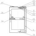
如图1至图3所示,本发明实施例的扫描电镜中的扫描透射成像装置包括样品台1、固定座2、支撑框3和背散射电子探头(图中未示出)。As shown in FIGS. 1 to 3 , the scanning transmission imaging device in the scanning electron microscope according to the embodiment of the present invention includes a
其中样品台1设置于支撑框3顶端,用于固定待观察样品;The
背散射电子探头设置于固定座2上,用于接收穿过待观察样品的透射散射电子;The backscattered electron probe is arranged on the
固定座2设置于支撑框3内,并与支撑框3连接,用于调节背散射电子探头距样品台1的距离。The fixing
本发明实施例中,待观察样品为薄样品,通常为Φ3mm薄样品;固定座2与支撑框3的连接方式可为滑动连接、卡接等连接方式。In the embodiment of the present invention, the sample to be observed is a thin sample, usually a thin sample of Φ3mm; the connection mode of the fixing
本发明的扫描电镜中的扫描透射成像装置,使用扫描电镜自带的背散射电子探头做透射散射电子信号探测器,不需要单独购买STEM附件,可大幅降低扫描电镜升级扫描透射成像功能的成本。同时,本发明的扫描电镜中的扫描透射成像装置可显著减少电子束对待观察样品的损伤,特别适合于有机高分子、生物等软材料样品的透射分析。The scanning transmission imaging device in the scanning electron microscope of the present invention uses the backscattered electron probe provided with the scanning electron microscope as the transmission scattering electron signal detector, and does not need to purchase STEM accessories separately, which can greatly reduce the cost of upgrading the scanning transmission imaging function of the scanning electron microscope. At the same time, the scanning transmission imaging device in the scanning electron microscope of the present invention can significantly reduce the damage of the sample to be observed by the electron beam, and is especially suitable for transmission analysis of soft material samples such as organic polymers and biology.
本发明的背散射电子探头的固定座2与支撑框3连接,可根据需要调节背散射电子探头距样品台1的距离,从而改变透射散射电子接收角的大小,进而实现高角环形暗场像(High-AngleAnnular Dark-Field Imaging,HAADF)和低角环形暗场像(Low-AngleAnnular Dark-Field Imaging,LAADF)的采集,使得所得图像能更加准确反映出待观察样品的结构与成分信息。The fixing
进一步地,本发明的支撑框3的结构如图4至图6所示,包括框体31、样品台凹槽32、滑轨槽33和第一固定螺丝34。Further, the structure of the
其中样品台凹槽32开设于框体31的顶端,样品台凹槽32内设置有透射通孔37,待观察样品设置于样品台凹槽32内;The
滑轨槽33设置于框体31的相对两侧;The
第一固定螺丝34穿过滑轨槽33与固定座2连接,用于将固定座2固定在框体31上。The first fixing
为保证待观察样品在测试过程中不会移动,本发明实施例的支撑框3还包括弹性压片35,弹性压片35设置于框体31的顶端;In order to ensure that the sample to be observed will not move during the test process, the
弹性压片35的一端与框体31的顶端固定连接,另一端设置于样品台1上,用于将样品台1固定于样品台凹槽32内。本发明实施例中,弹性压片35一端与框体31使用螺丝固定连接。One end of the elastic
为保证样品台1的导电性和稳定性,本发明实施例还在框体31的底端开设有与扫描电镜的样品台底座连接的连接孔36。In order to ensure the conductivity and stability of the
为便于灵活拆装样品台1,本发明实施例将样品台1设置为包括支撑片11和盖片12的结构,如图7至图10所示。In order to facilitate the flexible disassembly and assembly of the
其中支撑片11的第一表面上开设有样品凹槽111,样品凹槽111用于承载待观察样品;The first surface of the
盖片12固定于支撑片11上,盖片12的第一表面与待观察样品相接,用于将待观察样品固定于样品凹槽111内。本发明实施例中,盖片12的第一表面为平面。The
该种结构的样品台1,可实现在电镜外部更换样品,更换后再将样品台1固定到支撑框3上,可大幅缩短更换样品的时间。The
为达到同时采集待观察样品的扫描透射像和二次电子像的目的,本发明实施例在支撑片11的第二表面上开设有第一漏斗形凹槽112,第一漏斗形凹槽112与样品凹槽111相接,且第一漏斗形凹槽112在支撑片11的第二表面上的直径大于第一漏斗形凹槽112与样品凹槽111相接处的直径。In order to achieve the purpose of simultaneously collecting the scanning transmission image and the secondary electron image of the sample to be observed, a first funnel-shaped
本发明实施例还在盖片12的第二表面上开设有第二漏斗形凹槽121,第二漏斗形凹槽121在盖片12的第二表面上的直径大于第二漏斗形凹槽121在盖片12的第一表面上的直径。In the embodiment of the present invention, a second funnel-shaped
本发明样品台1上下面均为漏斗形凹槽,不会遮挡透射电子信号和二次电子信号,故可以达到同时采集待观察样品的扫描透射像和二次电子像的目的。The upper and lower surfaces of the
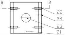
本发明实施例中,固定座2的结构如图11和图12所示,固定座2上开设有固定凹槽21,固定凹槽21用于固定背散射电子探头;In the embodiment of the present invention, the structure of the fixing
固定凹槽21相对两侧的凸台25上开设有第一螺纹孔22;The
第一固定螺丝34依次穿过滑轨槽33与第一螺纹孔22,将固定座2固定在框体31上。The first fixing
其中固定凹槽21上开设有透射孔23,背散射电子探头的内孔与透射孔23相匹配,具体为背散射电子探头的内孔与透射孔23大小相同、位置对应。The fixing
本发明实施例中,使用扫描电镜自带的背散射电子探头做透射散射电子信号探测器,背散射电子探头为环形,内孔的直径略大于样品直径(Φ3mm),散射角较小的透射电子可以穿过内孔,散射角较大的透射电子则会被环形探头收集,形成环形暗场像(AnnularDark-Field Imaging,ADF)。由于散射角较小的透射电子不会直接照射在信号探测面上,因此可以避免信号的过饱和问题。In the embodiment of the present invention, the backscattered electron probe that comes with the scanning electron microscope is used as the transmission scattering electron signal detector. The backscattered electron probe is annular, the diameter of the inner hole is slightly larger than the diameter of the sample (Φ3mm), and the transmission electrons with a smaller scattering angle are used. It can pass through the inner hole, and the transmitted electrons with larger scattering angle are collected by the annular probe to form an annular dark-field image (Annular Dark-Field Imaging, ADF). Since the transmitted electrons with smaller scattering angles do not directly irradiate the signal detection surface, the problem of signal supersaturation can be avoided.
为进一步固定背散射电子探头,本发明实施例在固定凹槽21相对两侧的凸台25上还开设有第二螺纹孔24;In order to further fix the backscattered electron probe, in the embodiment of the present invention, second threaded
第二固定螺丝穿过第二螺纹孔24,与固定凹槽21内的背散射电子探头相接,用于固定背散射电子探头。The second fixing screw passes through the second threaded
本发明实施例的固定座2采用绝缘性较好的塑料制作,使背散射电子探头与支撑框绝缘,避免背散射电子探头反馈碰触信号、造成扫描电镜样品台底座锁轴及不能正常操作电镜的问题。The fixing
本发明实施例的样品台1和支撑框3的材质为铝合金,具有质轻、高强、导电性好、价格低等优点,使得利用其制备的扫描电镜中的扫描透射成像装置,具有质量轻、导电性好、对扫描电镜样品台底座压迫小、使用寿命长、成本低等优点。The material of the
本发明通过固定座和支撑框的结合使用,可实现调节背散射电子探头距样品台的距离的目的,进一步实现使用扫描电镜自带的背散射电子探头接收透射散射电子信号的功能。本发明可显著减少电子束对待观察样品的损伤,适合于耐电子束辐照性较差样品的透射分析。The invention can realize the purpose of adjusting the distance between the backscattered electron probe and the sample stage through the combined use of the fixed seat and the support frame, and further realize the function of using the backscattered electron probe provided with the scanning electron microscope to receive the transmission scattered electron signal. The invention can significantly reduce the damage of the sample to be observed by the electron beam, and is suitable for the transmission analysis of the sample with poor resistance to electron beam irradiation.
本发明以FEI Quanta 650FEG扫描电镜为例,说明本发明装置的使用方法:The present invention takes FEI Quanta 650FEG scanning electron microscope as an example to illustrate the use method of the device of the present invention:
(1)打开扫描电镜样品室,取下样品台固定盘,将支撑框3放在样品台底座上,使支撑框3底端的连接孔36与样品台底座上的螺纹孔对齐,并用螺丝穿过连接孔36将支撑框3固定在扫描电镜样品台底座上。(1) Open the SEM sample chamber, remove the sample stage fixing plate, place the
(2)将扫描电镜背散射电子探头放在固定座2的固定凹槽21内,使背散射电子探头的信号探测面朝外、中心孔与固定座2的透射孔23对齐,并用固定座2两侧凸台25内的第二固定螺丝将其固定。(2) Put the scanning electron microscope backscattered electron probe in the fixing
(3)将装配好探头的固定座2放在支撑框3内,使背散射电子探头信号探测面朝上、固定座2的第一螺纹孔22与支撑框3的滑轨槽33对齐,并用第一固定螺丝34穿过支撑框3的滑轨槽33与固定座2内的第一螺纹孔22,从而将固定座2与支撑框3连接在一起。(3) Put the fixed
(4)测量背散射电子探头的信号探测面与支撑框3的透射通孔37的距离,用支撑框3的滑轨槽33内的第一固定螺丝34将固定座2固定于支撑框3上,本实施例中背散射电子探头的信号探测面与透射通孔37的距离为12mm。(4) Measure the distance between the signal detection surface of the backscattered electron probe and the transmission through
(5)将待观察样品放在支撑片11的样品凹槽111内,用盖片12的第一表面将其压住,并用螺丝穿过盖片12的通孔拧入支撑片11的螺纹孔内,将待观察样品夹持在支撑片11和盖片12之间。本实施例中的待观察样品为Φ3mm薄样品。(5) Put the sample to be observed in the
(6)将组装好的样品台1放在支撑框3顶端的样品台凹槽32内,用支撑框3顶端的弹性压片35将样品台1固定在样品台凹槽32内。(6) Place the assembled
(7)关闭扫描电镜样品室,对样品室抽真空后即可进行观察,观察过程中可以同时展现扫描透射环形暗场(STEM-ADF)像和二次电子(SE)像,其中STEM-ADF像仅通过选择扫描电镜操作界面中的BSED探头即可实现成像。(7) Close the SEM sample chamber, and the sample chamber can be observed after evacuating the sample chamber. During the observation process, the scanning transmission annular dark field (STEM-ADF) image and the secondary electron (SE) image can be displayed at the same time. The STEM-ADF image Imaging can be achieved simply by selecting the BSED probe in the SEM operator interface.
(8)测试完成后,给扫描电镜样品室放气,打开样品室即可更换样品或取下扫描透射成像装置。(8) After the test is completed, vent the sample chamber of the scanning electron microscope, and open the sample chamber to replace the sample or remove the scanning transmission imaging device.
以上所述,仅是本申请的几个实施例,并非对本申请做任何形式的限制,虽然本申请以较佳实施例揭示如上,然而并非用以限制本申请,任何熟悉本专业的技术人员,在不脱离本申请技术方案的范围内,利用上述揭示的技术内容做出些许的变动或修饰均等同于等效实施案例,均属于技术方案范围内。The above are only a few embodiments of the present application, and are not intended to limit the present application in any form. Although the present application is disclosed as above with preferred embodiments, it is not intended to limit the present application. Without departing from the scope of the technical solution of the present application, any changes or modifications made by using the technical content disclosed above are equivalent to equivalent implementation cases and fall within the scope of the technical solution.
Claims (10)
Translated fromChinesePriority Applications (1)
| Application Number | Priority Date | Filing Date | Title |
|---|---|---|---|
| CN202210329055.1ACN114695040B (en) | 2022-03-31 | 2022-03-31 | A scanning transmission imaging device in a scanning electron microscope |
Applications Claiming Priority (1)
| Application Number | Priority Date | Filing Date | Title |
|---|---|---|---|
| CN202210329055.1ACN114695040B (en) | 2022-03-31 | 2022-03-31 | A scanning transmission imaging device in a scanning electron microscope |
Publications (2)
| Publication Number | Publication Date |
|---|---|
| CN114695040Atrue CN114695040A (en) | 2022-07-01 |
| CN114695040B CN114695040B (en) | 2025-03-25 |
Family
ID=82141300
Family Applications (1)
| Application Number | Title | Priority Date | Filing Date |
|---|---|---|---|
| CN202210329055.1AActiveCN114695040B (en) | 2022-03-31 | 2022-03-31 | A scanning transmission imaging device in a scanning electron microscope |
Country Status (1)
| Country | Link |
|---|---|
| CN (1) | CN114695040B (en) |
Cited By (1)
| Publication number | Priority date | Publication date | Assignee | Title |
|---|---|---|---|---|
| CN115763200A (en)* | 2022-12-09 | 2023-03-07 | 内蒙古工业大学 | Multi-station scanning transmission bright field image imaging device |
Citations (5)
| Publication number | Priority date | Publication date | Assignee | Title |
|---|---|---|---|---|
| EP2075821A2 (en)* | 2007-12-26 | 2009-07-01 | Jeol Ltd. | Sample holder, method for observation and inspection, and apparatus for observation and inspection |
| CN203479832U (en)* | 2013-06-17 | 2014-03-12 | 北京师范大学 | Scanning-transmission-image observing apparatus used for scanning electron microscope |
| CN107437488A (en)* | 2017-07-24 | 2017-12-05 | 武汉华星光电技术有限公司 | A kind of focused ion beam microscope board |
| KR20200082299A (en)* | 2018-12-28 | 2020-07-08 | 참엔지니어링(주) | Apparatus and method for observing specimen |
| CN213364632U (en)* | 2020-06-16 | 2021-06-04 | 北京师范大学 | Sample holder for observing backscattered electron image by scanning electron microscope |
- 2022
- 2022-03-31CNCN202210329055.1Apatent/CN114695040B/enactiveActive
Patent Citations (6)
| Publication number | Priority date | Publication date | Assignee | Title |
|---|---|---|---|---|
| EP2075821A2 (en)* | 2007-12-26 | 2009-07-01 | Jeol Ltd. | Sample holder, method for observation and inspection, and apparatus for observation and inspection |
| US20090166536A1 (en)* | 2007-12-26 | 2009-07-02 | Jeol Ltd. | Sample Holder, Method for Observation and Inspection, and Apparatus for Observation and Inspection |
| CN203479832U (en)* | 2013-06-17 | 2014-03-12 | 北京师范大学 | Scanning-transmission-image observing apparatus used for scanning electron microscope |
| CN107437488A (en)* | 2017-07-24 | 2017-12-05 | 武汉华星光电技术有限公司 | A kind of focused ion beam microscope board |
| KR20200082299A (en)* | 2018-12-28 | 2020-07-08 | 참엔지니어링(주) | Apparatus and method for observing specimen |
| CN213364632U (en)* | 2020-06-16 | 2021-06-04 | 北京师范大学 | Sample holder for observing backscattered electron image by scanning electron microscope |
Cited By (2)
| Publication number | Priority date | Publication date | Assignee | Title |
|---|---|---|---|---|
| CN115763200A (en)* | 2022-12-09 | 2023-03-07 | 内蒙古工业大学 | Multi-station scanning transmission bright field image imaging device |
| CN115763200B (en)* | 2022-12-09 | 2023-11-07 | 内蒙古工业大学 | A multi-station scanning transmission bright field imaging device |
Also Published As
| Publication number | Publication date |
|---|---|
| CN114695040B (en) | 2025-03-25 |
Similar Documents
| Publication | Publication Date | Title |
|---|---|---|
| US7582885B2 (en) | Charged particle beam apparatus | |
| JP4923716B2 (en) | Sample analysis apparatus and sample analysis method | |
| US20080006771A1 (en) | Electron beam apparatus to collect side-view and/or plane-view image with in-lens sectional detector | |
| CN110987995B (en) | Universal sample holder for scanning electron microscope and in-situ mechanical test and three-dimensional atomic probe equipment | |
| WO1995004367A1 (en) | Improved environmental scanning electron microscope | |
| WO2010016504A1 (en) | Inspection device | |
| CN114695040A (en) | Scanning transmission imaging device in scanning electron microscope | |
| CN113325021B (en) | An in-situ testing method and a sample stage capable of carrying micro-nanoscale samples | |
| KR101398456B1 (en) | Specimen holder for observing top section of specimen and method for controlling thereof | |
| JP2015056395A (en) | Sample holder used for cross-sectional observation of sample and control method thereof | |
| CN103700562A (en) | Height adjustment type scanning electron microscope sampler holder | |
| JP5450357B2 (en) | Scanning electron microscope | |
| CN202421509U (en) | Cold cathode auxiliary power spectrum system | |
| CN116092906B (en) | In-situ characterization universal sample stage and method for focused ion beam and nano ion probe | |
| US2277024A (en) | Electronic microscope | |
| CN112461880B (en) | Method for positioning and detecting surface conductive type passage of glass sealing structure | |
| CN201455590U (en) | Filament welding fixture of scanning electronic microscope | |
| JP2014044967A (en) | Scanning electron microscope and sample holder | |
| CN221811770U (en) | A scanning electron microscope imaging system | |
| CN205140924U (en) | Quick positioner of scanning electron microscope sample microdomain | |
| CN210923481U (en) | Microscope temperature control fine adjustment objective table | |
| US20020064886A1 (en) | Apparatus and method for sampling | |
| CN114578097A (en) | High-vacuum low-temperature atomic force microscope optical path system below 4.2K | |
| CN217387075U (en) | Imaging device for scanning transmission bright field image in scanning electron microscope | |
| CN221667840U (en) | Sample stage for observing electron beam induced current of section sample |
Legal Events
| Date | Code | Title | Description |
|---|---|---|---|
| PB01 | Publication | ||
| PB01 | Publication | ||
| SE01 | Entry into force of request for substantive examination | ||
| SE01 | Entry into force of request for substantive examination | ||
| GR01 | Patent grant | ||
| GR01 | Patent grant |