CN114692073A - Data processing method and circuit based on convolution operation - Google Patents
Data processing method and circuit based on convolution operationDownload PDFInfo
- Publication number
- CN114692073A CN114692073ACN202210375356.8ACN202210375356ACN114692073ACN 114692073 ACN114692073 ACN 114692073ACN 202210375356 ACN202210375356 ACN 202210375356ACN 114692073 ACN114692073 ACN 114692073A
- Authority
- CN
- China
- Prior art keywords
- convolution
- input data
- coordinate
- size
- data
- Prior art date
- Legal status (The legal status is an assumption and is not a legal conclusion. Google has not performed a legal analysis and makes no representation as to the accuracy of the status listed.)
- Pending
Links
Images


Classifications
- G—PHYSICS
- G06—COMPUTING OR CALCULATING; COUNTING
- G06F—ELECTRIC DIGITAL DATA PROCESSING
- G06F17/00—Digital computing or data processing equipment or methods, specially adapted for specific functions
- G06F17/10—Complex mathematical operations
- G06F17/15—Correlation function computation including computation of convolution operations
- G06F17/153—Multidimensional correlation or convolution
- G—PHYSICS
- G06—COMPUTING OR CALCULATING; COUNTING
- G06F—ELECTRIC DIGITAL DATA PROCESSING
- G06F5/00—Methods or arrangements for data conversion without changing the order or content of the data handled
- G06F5/06—Methods or arrangements for data conversion without changing the order or content of the data handled for changing the speed of data flow, i.e. speed regularising or timing, e.g. delay lines, FIFO buffers; over- or underrun control therefor
- G06F5/065—Partitioned buffers, e.g. allowing multiple independent queues, bidirectional FIFO's
Landscapes
- Engineering & Computer Science (AREA)
- Physics & Mathematics (AREA)
- Theoretical Computer Science (AREA)
- General Physics & Mathematics (AREA)
- General Engineering & Computer Science (AREA)
- Computational Mathematics (AREA)
- Mathematical Analysis (AREA)
- Mathematical Optimization (AREA)
- Pure & Applied Mathematics (AREA)
- Data Mining & Analysis (AREA)
- Mathematical Physics (AREA)
- Algebra (AREA)
- Software Systems (AREA)
- Databases & Information Systems (AREA)
- Computing Systems (AREA)
- Image Processing (AREA)
Abstract
Description
Translated fromChinese技术领域technical field
本发明涉及一种数据处理机制,且特别是有关于一种基于卷积运算的 数据处理方法及电路。The present invention relates to a data processing mechanism, and in particular, to a data processing method and circuit based on convolution operations.
背景技术Background technique
神经网络是人工智能(Artificial Intelligence,AI)中的一个重要主 题,并是通过仿真人类脑细胞的运作来进行决策。值得注意的是,人类脑细 胞中存在着许多神经元(Neuron),且这些神经元会通过突触(Synapse)来互相 连结。各神经元可经由突触接收讯号,且这讯号经转化后的输出会再传导到 另一个神经元。各神经元的转化能力不同,且人类通过前述讯号传递与转化 的运作,可形成思考与确定的能力。神经网络即是根据前述运作方式来得到 对应能力。Neural networks are an important topic in artificial intelligence (AI), and make decisions by simulating the operation of human brain cells. It is worth noting that there are many neurons (Neurons) in human brain cells, and these neurons are connected to each other through synapses (Synapse). Each neuron receives a signal through a synapse, and the transformed output of this signal is transmitted to another neuron. The transformation ability of each neuron is different, and through the operation of the aforementioned signal transmission and transformation, human beings can form the ability to think and determine. The neural network obtains the corresponding ability according to the aforementioned operation method.
在神经网络的运作中,输入向量与对应突触的权重进行卷积运算,从而 撷取特征。值得注意的是,输入值及权重值的数量可能很多,但现有架构针 对大数量的资料通常会遭遇到较高功耗、较常等待时间及较多空间用量等问 题。In the operation of the neural network, the input vector is convolved with the weight of the corresponding synapse to extract features. It is worth noting that the number of input values and weight values may be large, but existing architectures usually suffer from higher power consumption, higher latency, and higher space usage for large amounts of data.
发明内容SUMMARY OF THE INVENTION
本发明实施例是针对一种基于卷积运算的数据处理方法及电路,可提供 还有效率的数据配置。Embodiments of the present invention are directed to a data processing method and circuit based on convolution operation, which can provide efficient data configuration.
根据本发明的实施例,基于卷积运算的数据处理方法包括(但不仅限于) 下列步骤:提供总和缓存器。根据总和缓存器的大小读取数个卷积核(kernel) 中的卷积核组。卷积核组中的那些卷积核的数量相同于总和缓存器的大小。 将输入数据与第一卷积核组的卷积运算结果通过先入先出(First Input First Output,FIFO)暂存在总和缓存器。According to an embodiment of the present invention, the data processing method based on the convolution operation includes (but is not limited to) the following steps: providing a sum buffer. The convolution kernel groups in several convolution kernels (kernels) are read according to the size of the sum buffer. The number of those kernels in the kernel group is the same as the sum buffer size. The result of the convolution operation between the input data and the first convolution kernel group is temporarily stored in the summation buffer through a first-in, first-out (First Input First Output, FIFO).
根据本发明的实施例,基于卷积运算的数据处理电路包括(但不仅限于) 一个或更多个存储器及处理器。存储器用以存储程序代码。处理器耦接存储 器。处理器经配置用以加载且执行程序代码以执行下列步骤:提供总和缓存 器。根据总和缓存器的大小读取数个卷积核中的卷积核组。卷积核组中的那 些卷积核的数量相同于总和缓存器的大小。将输入数据与第一卷积核组的卷 积运算结果通过先入先出暂存在总和缓存器。According to an embodiment of the present invention, a data processing circuit based on a convolution operation includes (but is not limited to) one or more memories and a processor. The memory is used to store program codes. The processor is coupled to the memory. The processor is configured to load and execute program code to perform the steps of: providing a summation register. Read the convolution kernel group in several convolution kernels according to the size of the sum buffer. The number of those kernels in the kernel group is the same as the sum buffer size. The result of the convolution operation between the input data and the first convolution kernel group is temporarily stored in the sum register through first-in, first-out.
基于上述,根据本发明实施例的基于卷积运算的数据处理方法及电路, 可分批形成且处理多组卷积核组,从而有效地利用存储器空间,并可提升运 算效率。Based on the above, according to the data processing method and circuit based on convolution operation according to the embodiment of the present invention, multiple groups of convolution kernel groups can be formed and processed in batches, so as to effectively utilize the memory space and improve the operation efficiency.
附图说明Description of drawings
包含附图以便进一步理解本发明,且附图并入本说明书中并构成本说 明书的一部分。附图说明本发明的实施例,并与描述一起用于解释本发明 的原理。The accompanying drawings are included to provide a further understanding of the present invention, and are incorporated in and constitute a part of this specification. The drawings illustrate embodiments of the invention and together with the description serve to explain the principles of the invention.
图1是根据本发明一实施例的数据处理电路的组件方块图;1 is a block diagram of components of a data processing circuit according to an embodiment of the present invention;
图2是根据本发明一实施例的数据处理方法-存储配置的流程图;2 is a flowchart of a data processing method-storage configuration according to an embodiment of the present invention;
图3是根据本发明一实施例的输入资料的示意图;3 is a schematic diagram of input data according to an embodiment of the present invention;
图4是根据本发明一实施例的多存储器的存储空间的示意图;4 is a schematic diagram of a storage space of a multi-memory according to an embodiment of the present invention;
图5A是根据本发明一实施例的多存储器的存储配置的示意图;5A is a schematic diagram of a storage configuration of multiple memories according to an embodiment of the present invention;
图5B是根据本发明一实施例的多存储器的存储配置的示意图;5B is a schematic diagram of a storage configuration of multiple memories according to an embodiment of the present invention;
图5C是根据本发明一实施例的多存储器的存储配置的示意图;5C is a schematic diagram of a storage configuration of multiple memories according to an embodiment of the present invention;
图6是根据本发明一实施例的数据处理方法-填充扩展的流程图;6 is a flowchart of a data processing method-filling extension according to an embodiment of the present invention;
图7A是根据本发明一实施例的输入资料的示意图;7A is a schematic diagram of input data according to an embodiment of the present invention;
图7B是根据本发明一实施例的经填充的输入数据的示意图;7B is a schematic diagram of padded input data according to an embodiment of the invention;
图8是根据本发明一实施例的共享存储器的示意图;8 is a schematic diagram of a shared memory according to an embodiment of the present invention;
图9是根据本发明一实施例的数据处理方法-运算配置的流程图;9 is a flowchart of a data processing method-operation configuration according to an embodiment of the present invention;
图10是根据本发明一实施例的卷积运算的示意图;10 is a schematic diagram of a convolution operation according to an embodiment of the present invention;
图11是根据本发明一实施例的卷积运算的示意图;11 is a schematic diagram of a convolution operation according to an embodiment of the present invention;
图12是根据本发明一实施例的卷积运算的示意图;12 is a schematic diagram of a convolution operation according to an embodiment of the present invention;
图13是根据本发明一实施例的并行运算的示意图;13 is a schematic diagram of parallel operations according to an embodiment of the present invention;
图14是根据本发明一实施例的资料重复的示意图;14 is a schematic diagram of data duplication according to an embodiment of the present invention;
图15是根据本发明一实施例的资料重复的示意图;15 is a schematic diagram of data duplication according to an embodiment of the present invention;
图16是根据本发明一实施例的整体数据处理的流程图。FIG. 16 is a flowchart of overall data processing according to an embodiment of the present invention.
附图标号说明Explanation of reference numerals
100:数据处理电路;100: data processing circuit;
110、M1~M8:存储器;110. M1~M8: memory;
150:处理器;150: processor;
151:处理组件;151: processing components;
S210~S230、S610~S650、S910~S950、S1610~S1660:步骤;S210~S230, S610~S650, S910~S950, S1610~S1660: steps;
x:宽;x: width;
y:高;y: high;
z:通道数;z: number of channels;
D1、Pixel、Pixel1~:Pixelj输入数据;D1, Pixel, Pixel1~: Pixelj input data;
W:宽度;W:width;
x0~x6、y0~y6:坐标;x0~x6, y0~y6: coordinates;
n:正整数;n: positive integer;
CMD:指令;cmd:command;
Arb:仲裁器;Arb: Arbiter;
Bk0~Bkm-1:存储器库;Bk0 ~ Bkm-1 : memory bank;
DATA:资料;DATA: data;
rch0~rch3:所欲读取数据;rch0~rch3: the data you want to read;
wch0~wch3:所欲写入资料;wch0~wch3: the data you want to write;
rch0_rdata~rch3_rdata:所读取的数据;rch0_rdata~rch3_rdata: the data read;
WT、K1~K128:卷积核;WT, K1~K128: convolution kernel;
ch1~ch128:通道;ch1~ch128: channel;
OT:输出缓存器;OT: output buffer;
SB:总和缓存器。SB: Sum Buffer.
具体实施方式Detailed ways
现将详细地参考本发明的示范性实施例,示范性实施例的实例说明于附 图中。只要有可能,相同组件符号在图式和描述中用来表示相同或相似部分。Reference will now be made in detail to the exemplary embodiments of the present invention, examples of which are illustrated in the accompanying drawings. Wherever possible, the same reference numerals are used in the drawings and description to refer to the same or similar parts.
图1是根据本发明一实施例的数据处理电路100的组件方块图。请参照 图1,数据处理电路100包括(但不仅限于)一个或更多个存储器110及处理 器150。FIG. 1 is a block diagram of components of a
存储器110可以是静态或动态随机存取存储器(Random Access Memory, RAM)、只读存储器(Read-Only Memory,ROM)、快闪存储器(Flash Memory)、 寄存器(Register)、组合逻辑电路(Combinational Circuit)或上述组件的组 合。在一实施例中,存储器110用于乘积累加运算(Multiply Accumulate, MAC)或卷积运算所用的输入数据、卷积核(kernel)、权重、激励(activation) 运算、池化(pooling)运算及/或其他神经网络运算所用的数值。在其他实施 例中,应用者可根据实际需求而确定存储器110所存储数据的类型。在一实 施例中,存储器110用以存储程序代码、软件模块、组态配置、数据或档案, 并待后续实施例详述。The
处理器150耦接存储器110。处理器150可以是由多任务器、加法器、 乘法器、编码器、译码器、或各类型逻辑闸中的一者或更多者所组成的电路, 并可以是中央处理单元(Central Processing Unit,CPU)、图形处理单元 (Graphic Processing unit,GPU),或是其他可程序化的一般用途或特殊用 途的微处理器(Microprocessor)、数字信号处理器(Digital Signal Processor,DSP)、可程序化控制器、现场可程序化逻辑门阵列(FieldProgrammable Gate Array,FPGA)、特殊应用集成电路(Application-SpecificIntegrated Circuit,ASIC)、神经网络加速器或其他类似组件或上述组件的 组合。在一实施例中,处理器150经配置用以执行数据处理电路100的所有 或部份作业,且可加载并执行存储器110所存储的各软件模块、程序代码、 档案及数据。在一些实施例中,处理器150的运作可通过软件实现。The
在一实施例中,处理器150包括一个或更多个处理组件(Processing Element,PE)151。这些处理组件151经组态执行相同或不同指令规定的操作。 例如,卷积运算、矩阵运算或其他运算。In one embodiment, the
下文中,将搭配数据处理电路100中的各项组件或电路说明本发明实施 例所述的方法。本方法的各个流程可依照实施情形而调整,且并不仅限于此。Hereinafter, the method according to the embodiment of the present invention will be described in conjunction with various components or circuits in the
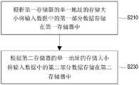
图2是根据本发明一实施例的数据处理方法-存储配置的流程图。请参照 图2,处理器150根据数个存储器110中的第一存储器的单一地址(下文称这 存储器110的某一个地址为第一地址)的存储空间大小将输入数据中的第一 部分数据存储在存储器110中。具体而言,每次待处理的输入数据的大小不 一定相同。举例而言,图3是根据本发明一实施例的输入资料D1的示意图。 请参照图3,输入数据D1的大小/尺寸为宽x*高y*通道数z。即,输入数据 D1包括x*y*z个元素。若以坐标系为例,则输入数据D1中在通道数z为零 的那些元素的坐标可标示为:FIG. 2 is a flowchart of a data processing method-storage configuration according to an embodiment of the present invention. Referring to FIG. 2 , the
表(1)Table 1)
须说明的是,表(1)所示的宽x及高y的数值仅作为范例说明,且通道数 z可能是8、16、32或其他数值。此外,输入数据可能是用于后续卷积运算 或其他运算所用的感测值、影像、检测数据、特征图(feature map)、卷积核 (kernel)、或权重,并可视应用者的实际需求而自行变更其内容。It should be noted that the values of width x and height y shown in Table (1) are only for illustration, and the number of channels z may be 8, 16, 32 or other values. In addition, the input data may be sensed values, images, detection data, feature maps, convolution kernels, or weights used for subsequent convolution operations or other operations, depending on the actual situation of the user. Change its content as required.
值得注意的是,数据存储在存储器110的位置可能会影响后续存取数据 的效率及空间使用率。在本发明实施例中,这第一部分数据的大小不大于第 一地址的存储空间大小。换句而言,处理器150将输入数据根据单一地址所 提供的存储空间大小来拆分出多个部分数据,并将输入数据中的部分数据存 储在存储器110中。这处部分数据代表输入数据中的部分或全部。It is worth noting that the location where data is stored in
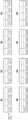
在一实施例中,处理器150比较输入数据的通道数量与第一地址的存储 空间大小。各存储器110包括一个或更多个存储器地址(例如,前述第一地 址),且各存储器地址提供一定的存储空间大小供数据存储。举例而言,图4 是根据本发明一实施例的多存储器的存储空间的示意图。请参照图4,假设 数据处理电路100包括存储器M1~M8,且各存储器M1~M8的单一地址的宽度 W(即,存储空间)为32字节(byte)。In one embodiment, the
图5A是根据本发明一实施例的多存储器的存储配置的示意图。请参照图 4及图5A,假设输入数据的大小为7×7×8,则处理器150比较通道数(即, 8)及第一地址的宽度(即,32),并得出比较结果为宽度为四倍的通道数。5A is a schematic diagram of a storage configuration of multiple memories according to an embodiment of the present invention. Referring to FIG. 4 and FIG. 5A , assuming that the size of the input data is 7×7×8, the
图5B是根据本发明一实施例的多存储器的存储配置的示意图。请参照图 4及图5B,假设输入数据的大小为7×7×16,则处理器150比较通道数(即, 16)及第一地址的宽度(即,32),并得出比较结果为宽度为两倍的通道数。5B is a schematic diagram of a storage configuration of multiple memories according to an embodiment of the present invention. Referring to FIG. 4 and FIG. 5B , assuming that the size of the input data is 7×7×16, the
图5C是根据本发明一实施例的多存储器的存储配置的示意图。请参照图 4及图5C,假设输入数据的大小为7×7×64,则处理器150比较通道数(即, 64)及第一地址的宽度(即,32),并得出比较结果为通道数为两倍的宽度。5C is a schematic diagram of a storage configuration of multiple memories according to an embodiment of the present invention. Referring to FIG. 4 and FIG. 5C , assuming that the size of the input data is 7×7×64, the
处理器150可根据通道数量与第一地址的存储空间大小的比较结果确定 第一部分数据所包括的输入数据的元素的元素数量。在一实施例中,若处理 器150确定比较结果为通道数量未大于第一地址的存储空间大小,则进一步 确定通道数量与元素数量的乘积未大于第一地址的存储空间大小。The
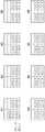
以图5A为例,单一地址的宽度为四倍的通道数。因此,元素数量可以是 4、3、2或1。以4个元素为例,存储器M1的地址n(正整数)存储输入数据 中的通道1~8且坐标为(x0,y0)(以表(1)的坐标系为例)、(x1,y0)、(x2,y0) 及(x3,y0)的元素。以图5B为例,宽度为两倍的通道数。因此,元素数量可 以是2或1。以2个元素为例,地址n存储输入数据中的通道1~8且坐标为 (x1,y0)及(x1,y0)的元素。由此可知,第一地址存储输入数据中的相同坐标 的多个通道的元素,且本发明实施例是以单一元素的所有通道优先分配。Taking FIG. 5A as an example, the width of a single address is four times the number of channels. Therefore, the number of elements can be 4, 3, 2 or 1. Taking 4 elements as an example, the address n (positive integer) of the memory
在另一实施例中,若处理器150确定比较结果为通道数量大于第一地址 的存储空间大小,则进一步确定第一部分数据所包括的元素数量为一。由于 单一地址的存储空间大小不足以存储单一元素的所有通道,因此处理器150 可拆分通道。In another embodiment, if the
以图5C为例,单一地址的通道数为两倍的宽度。因此,元素数量是1, 且处理器150将64个通道拆分成第1~32通道及第33~64通道。地址n存储 输入数据中的通道1~32且坐标为(x0,y0)的元素。Taking FIG. 5C as an example, the number of channels of a single address is twice as wide. Therefore, the number of elements is 1, and the
请参照图2,处理器150根据那些存储器110中的第二存储器的单一地 址(下文称这存储器110的某一个地址为第二地址)的存储大小将输入数据中 的第二部分数据存储在第二存储器中(步骤S230)。具体而言,这第二部分数 据的大小不大于第二地址的存储空间大小。值得注意的是,第一地址所存储 的第一部分数据在任一通道的输入数据的二维坐标中的坐标与第二地址所存 储的第二部分数据的坐标不同。即,处理器150继续处理输入数据中尚未被 存储的其他数据。同理地,在一实施例中,处理器150比较输入数据的通道 数量与第二地址的存储空间大小,并根据通道数量与第二地址的存储空间大 小的比较结果确定第二部分数据所包括的输入数据的元素的元素数量。Referring to FIG. 2 , the
在一实施例中,若处理器150确定比较结果为通道数量未大于第二地址 的存储空间大小,则进一步确定通道数量与元素数量的乘积未大于第二地址 的存储空间大小。以图5A及4个元素为例,存储器M2的地址n存储输入数 据中的通道1~8且坐标为(x4,y0)、(x5,y0)、(x6,y0)及(x7,y0)的元素(因坐 标(x0,y0)、(x1,y0)、(x2,y0)及(x3,y0)已存储在存储器M1,故依照顺序分 配)。以图5B且2个元素为例,存储器M2的地址n存储输入数据中的通道 1~8且坐标为(x2,y0)及(x3,y0)的元素。In one embodiment, if the
在另一实施例中,若处理器150确定比较结果为通道数量大于第二地址 的存储空间大小,则进一步确定第二部分数据所包括的元素数量为一。以图 5C为例且元素数量是1,存储器M2的地址n存储输入数据中的通道1~32且 坐标为(x1,y0)的元素。此外,依此类推,处理器150可分配其他部分数据至 其他存储器M3~M8。In another embodiment, if the
在一实施例中,处理器150可根据第一存储器的第三地址(不同于第一地 址)的存储空间大小将输入数据中的第三部分数据存储在第一存储器的第三 地址中。这第三部分数据的大小不大于第三地址的存储空间大小。此外,第 三地址所存储的第三部分数据在任一通道的输入数据的二维坐标中的坐标与 第一地址所存储的第一部分数据的坐标可能相同或不同。In one embodiment, the
以图5C为例,存储器M1的地址n存储坐标为(x0,y0)的元素,存储器 M1的地址n+1存储坐标为(x1,y1)的元素,且存储器M1的地址n+7存储坐标 为(x0,y0)的元素。在一些实施例中,第三部分数据所包括的通道可能不同第 一部分数据所包括的通道。以图5C为例,存储器M1的地址n存储坐标为 (x1,y1)且通道1~32的元素,且地址n+7存储坐标为(x1,y1)且通道33~64的 元素。Taking FIG. 5C as an example, the address n of the memory M1 stores the element whose coordinates are (x0, y0), the address n+1 of the memory M1 stores the element whose coordinates are (x1, y1), and the address n+7 of the memory M1 stores the coordinates. is the element of (x0,y0). In some embodiments, the channels included in the third portion of data may be different from the channels included in the first portion of data. Taking FIG. 5C as an example, address n of memory M1 stores elements whose coordinates are (x1, y1) and
藉此,本发明实施例可充分地运用存储器110中的存储空间。In this way, the embodiment of the present invention can fully utilize the storage space in the
图6是根据本发明一实施例的数据处理方法-填充扩展的流程图。请参照 图6,处理器150根据填充(padding)模式扩展输入数据,以产生扩展的输入 数据(步骤S610)。具体而言,在一些应用情境中(例如,数据经卷积运算、 或保持边界信息的需求),需要扩展输入数据的大小,并可通过填充数据来达 成需求。填充模式可以是反射镜像(reflect mirror)模式或对称镜像 (symmetric mirror)模式。FIG. 6 is a flowchart of a data processing method - padding extension according to an embodiment of the present invention. Referring to FIG. 6, the
举例而言,输入数据如表(2)所示:For example, the input data is shown in Table (2):
表(2)Table 2)
若经反射镜像模式填充,则可得出:If filled with reflection mirror mode, it can be obtained:
表(3)table 3)
若经对称镜像模式填充,则可得出:If filled with symmetrical mirror mode, it can be obtained:
表(4)Table 4)
处理器150对扩展的输入数据中的多个元素提供二维坐标系的坐标(步 骤S630)。具体而言,以输入数据在单一通道下的宽与高而言,这些元素可 形成一个矩阵。若为这矩阵的各元素提供一个坐标,则可采用二维坐标系。 二维坐标系的横向轴对应于输入数据的宽,且坐标系的纵向轴对应于输入数 据的高。此外,轴上的任一整数值对应到输入数据的一个或更多个元素。The
在一实施例中,处理器150可设定未扩展的输入数据的坐标在第一维度(即,横向轴)介于0至w且在第二维度(即,纵向轴)介于0至h。w为未扩展 的输入数据的宽,且h为未扩展的输入数据的高。此外,处理器150可设定 扩展的输入资料中的不属于未扩展的输入数据的坐标在第一维度小于零或大 于w且在第二维度小于零或大于h。In one embodiment, the
举例而言,图7A是根据本发明一实施例的输入资料的示意图。请参照图 7A,宽为3且高为6的输入数据的坐标(x,y)中x为0~3且y为0~6。图7B 是根据本发明一实施例的经填充的输入数据(即,扩展的输入数据)的示意图。 请参照图7B,假设处理器150对输入数据的上面、下面、左边及右边向外各 填充两个元素,扩展的输入数据的坐标(x,y)中x为-2~5且y为-2~8。由此 可知,被填充的元素的坐标在x或y坐标小于零、x坐标大于w或y坐标大于h。值得注意的是,负值需要有符号数来表示,但有符号数不利于存储或 呼叫。For example, FIG. 7A is a schematic diagram of input data according to an embodiment of the present invention. Referring to FIG. 7A , in the coordinates (x, y) of the input data whose width is 3 and height is 6, x is 0-3 and y is 0-6. 7B is a schematic diagram of padded input data (ie, expanded input data) according to an embodiment of the present invention. Referring to FIG. 7B , it is assumed that the
请参照图6,处理器150根据位置信息读取扩展的输入数据中的那些元 素(步骤S650)。具体而言,位置信息包括未扩展的输入数据的大小及扩展的 输入数据中的那些元素的坐标。例如,位置信息为(w,h,c,x,y),其中w为输 入数据的宽,h为输入数据的高,c为输入数据的通道,x为某一元素在二维 坐标系中的横向轴的坐标,且y为这元素在二维坐标系中的纵向轴的坐标。 输入数据被存储在存储器110中。若欲读取输入数据中的特定元素,则处理 器150可根据这位置信息存取这元素。Referring to FIG. 6, the
与采用有符号数的坐标不同处,若位置信息中的某一个元素的坐标在这 二维坐标系中位于未扩展的输入资料以外,则处理器150根据填充模式转换 位置信息中的坐标。值得注意的是,位置信息中的坐标皆映像至未扩展的输 入数据的坐标。也就是说,位置信息中代表元素位置的坐标皆可对应至正值。Unlike coordinates using signed numbers, if the coordinates of an element in the position information lie outside the unexpanded input data in the two-dimensional coordinate system, the
以表(3)及表(4)为例,经填充的元素的数值皆相同于未扩展的输入数据 中的某一个元素的数值。因此,经填充的元素的坐标可由未扩展的输入数据 中具有相同数值的元素的坐标代替。Taking Table (3) and Table (4) as examples, the value of the filled elements is the same as the value of a certain element in the unextended input data. Therefore, the coordinates of the filled elements can be replaced by the coordinates of the elements with the same value in the unexpanded input data.
在一实施例中,假设未扩展的输入数据的宽为w且高为h,则处理器150 可确定位置信息所对应的某一元素的坐标在第一维度是否小于零或大于w, 并/或确定位置信息所对应的这元素的坐标在第二维度是否小于零或大于h。 若这坐标在第一维度小于零或大于w或在第二维度小于零或大于h,则处理 器150确定这元素是属于扩展的输入数据。相反而言,这坐标在第一维度未 小于零或未大于w或在第二维度未小于零或未大于h,则处理器150确定这 元素是属于未扩展的输入数据。In one embodiment, assuming that the width of the unextended input data is w and the height is h, the
针对坐标转换,在一实施例中,填充模式为反射镜像模式。若处理器150 确定位置信息所对应的某一元素的坐标在第一维度小于零,则进一步将这元 素在第一维度的第一坐标转变成第一坐标的绝对值。以数学式表示为:For coordinate transformation, in one embodiment, the filling mode is a reflective mirror mode. If the
若x<0,则ABS(x)…(1)If x<0, then ABS(x)...(1)
其中ABS()代表绝对值。where ABS() represents the absolute value.
若处理器150确定这位置信息所对应的这元素的坐标在第一维度大于w, 则进一步将这元素的第一坐标转变成第一坐标与两倍w的差值(或是w减去w 与第一坐标的差值取绝对值所得的值)。以数学式表示为:If the
若x>w,则(w-ABS(w-x))…(2)If x>w, then (w-ABS(w-x))...(2)
若处理器150确定这位置信息所对应的这元素的坐标在第二维度小于 零,则进一步将这元素在第二维度的第二坐标转变成第二坐标的绝对值。以 数学式表示为:If the
若y<0,则ABS(y)…(3)If y<0, then ABS(y)...(3)
若处理器150确定这位置信息所对应的这元素的坐标在第二维度大于h, 则进一步将这元素的第二坐标转变成第二坐标与两倍h的差值(或是h减去h 与第二坐标的差值取绝对值所得的值)。以数学式表示为:If the
若y>h,則(h-ABS(h-y))…(4)If y>h, then (h-ABS(h-y))...(4)
在另一实施例中,填充模式为对称镜像模式。若处理器150确定位置信 息所对应的某一元素的坐标在第一维度小于零,则进一步将这元素在第一维 度的第一坐标转变成第一坐标加一的绝对值。以数学式表示为:In another embodiment, the fill pattern is a symmetrical mirror pattern. If the
若x<0,则ABS(x+1)…(5)If x<0, then ABS(x+1)...(5)
若处理器150确定这位置信息所对应的这元素的坐标在第一维度大于w, 则进一步将这元素的第一坐标转变成第一坐标加一与两倍w的差值(或是w减 去第一坐标、w与1的差值取绝对值所得的值)。以数学式表示为:If the
若x>w,则(w-ABS(x-w-1))…(6)If x>w, then (w-ABS(x-w-1))...(6)
若处理器150确定这位置信息所对应的这元素的坐标在第二维度小于 零,则进一步将这元素在第二维度的第二坐标转变成第二坐标加一的绝对值。 以数学式表示为:If the
若y<0,则ABS(y+1)…(7)If y<0, then ABS(y+1)...(7)
若处理器150确定这位置信息所对应的这元素的坐标在第二维度大于h, 则进一步将这元素的第二坐标转变成第二坐标加一与两倍h的差值(或是h减 去第二坐标、h与1的差值取绝对值所得的值)。以数学式表示为:If the
若y>h,则(h-ABS(y-h-1))…(8)If y>h, then (h-ABS(y-h-1))...(8)
由此可知,处理器150可根据填充模式确定位置信息所指示的元素的数 值为未扩展的输入数据中一者。藉此,只要未扩展的输入数据的大小及填充 模式的类型,即可存取扩展的输入数据的元素。It can be seen from this that the
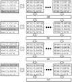
在一实施例中,为了有效率地存取存储器110所存储的数据,本发明实 施例还提出了分享存储器的架构。图8是根据本发明一实施例的共享存储器 的示意图。请参照图8,处理器150可将一个或更多个存储器110组合成一 个存储器库(bank)(例如,存储器库Bk0~Bkm-1(m为正整数)。各存储器库 Bk0~Bkm-1设有仲裁器(arbiter)Arb。In one embodiment, in order to efficiently access the data stored in the
在一实施例中,仲裁器Arb用以确定指令CMD所指示的存储位置。以图 8为例,假设图中所示8个指令CMD分别是用于读取数据(例如,前述输入数 据或卷积核/权重)的一个或更多个元素(例如,所欲读取数据rch0~rch3)以 及写入数据的一个或更多个元素(例如,所欲写入数据wch0~wch3)。在一实 施例中,指令CMD可包括指示元素的坐标的位置信息。例如,表(1)所示的二 维坐标系或结合通道的三维坐标系的坐标。在一实施例中,指令CMD可还包 括输入数据的大小。例如,输入数据的宽、高及/或通道。在一实施例中,指 令CMD可还包括填充模式。In one embodiment, the arbiter Arb is used to determine the storage location indicated by the command CMD. Taking FIG. 8 as an example, it is assumed that the 8 instructions CMD shown in the figure are respectively used to read one or more elements of data (for example, the aforementioned input data or convolution kernel/weight) (for example, the data to be read). rch0 to rch3) and one or more elements of the write data (for example, the data to be written wch0 to wch3). In one embodiment, the instruction CMD may include position information indicating the coordinates of the element. For example, the coordinates of the two-dimensional coordinate system shown in Table (1) or the three-dimensional coordinate system of the combined channel. In one embodiment, the instruction CMD may also include the size of the input data. For example, the width, height and/or channel of the input data. In one embodiment, the instruction CMD may further include a padding mode.
在一实施例中,各仲裁器Arb根据指令CMD的位置信息确定所指示元素 是否在所属的存储器库Bk0~Bkm-1内。若所指示的元素在所属的存储器库 Bk0~Bkm-1内,则这仲裁器Arb对所属的存储器库Bk0、Bk1、…或Bkm-1发出读取 或写入指令,以读取或写入这元素。若所指示的元素不在所属的存储器库 Bk0~Bkm-1内,则这仲裁器Arb忽略这指令CMD或禁能/不发出这元素的读取/ 写入指令。In one embodiment, each arbiter Arb determines whether the indicated element is in the memory bank Bk0 ˜Bkm-1 to which it belongs according to the position information of the instruction CMD. If the indicated element is in the memory bank Bk0 to Bkm-1 to which it belongs, the arbiter Arb issues a read or write command to the memory bank Bk0 , Bk1 , . . . or Bkm-1 to which it belongs, to Read or write this element. If the indicated element is not in the memory bank Bk0 ˜Bkm-1 to which it belongs, the arbiter Arb ignores the command CMD or disables/does not issue the read/write command for this element.
以图8为例,受仲裁器Arb确定读取输入数据的一个或更多个元素 rch0~rch3的指令CMD,即可读取出这些元素rch0~rch3的数据DATA(例如, 所读取的数据rch0_rdata~rch3_rdata)。Taking FIG. 8 as an example, the arbiter Arb determines the command CMD to read one or more elements rch0 to rch3 of the input data, and then the data DATA of these elements rch0 to rch3 (for example, the read data can be read out) rch0_rdata~rch3_rdata).
在一实施例中,各仲裁器Arb根据指令CMD的位置信息排序指令CMD。 仲裁器Arb所收到的两个或更多个指令CMD可能都存取相同元素。而仲裁器 Arb可排序这些指令CMD。In one embodiment, each arbiter Arb sorts the command CMD according to the position information of the command CMD. Two or more instructions CMD received by the arbiter Arb may both access the same element. And the arbiter Arb can order these instructions CMD.
在一实施例中,指令CMD及数据DATA根据先入先出(FIFO)机制输入或输 出指令CMD或数据DATA。先入先出缓存器可将第一个进入其内的指令CMD或 数据DATA第一个被移出,第二个进入其内的指令CMD或数据DATA第二个被 移出,其余顺序依次类推。藉此,可提供数据存取的效率。In one embodiment, the command CMD and the data DATA input or output the command CMD or the data DATA according to a first-in-first-out (FIFO) mechanism. The first-in, first-out register can move out the first command CMD or data DATA that entered into it first, and the second command CMD or data DATA entered into it to be moved out second, and so on. Thereby, the efficiency of data access can be improved.
图9是根据本发明一实施例的数据处理方法-运算配置的流程图。请参照 图9,处理器150提供总和缓存器(步骤S910)。具体而言,处理器150或处 理组件151可能经组态有特定大小的运算量。例如,单次运算量为3×3×32。 须说明的是,这运算量可能因规格或应用需求而不同,且本发明实施例不加 以限制。此外,总和缓存器是用于存储处理器150或处理组件151运算后所 输出的数据。然而,总和缓存器的大小可根据应用者的需求而变更,本发明 实施例不加以限制。FIG. 9 is a flowchart of a data processing method-operation configuration according to an embodiment of the present invention. Referring to FIG. 9, the
值得注意的是,所需运算的数据量可能超过运算量。例如,图10是根据 本发明一实施例的卷积运算的示意图。请参照图10,输入数据Pixel的大小 为3×3×128,卷积核WT的大小为3×3×128,且总共有128个卷积核 K1~K128。图中所示1~9代表输入数据Pixel中的一个通道的第1~9元素,或 是卷积核WT中的一个通道的第1~9元素。此外,图中所示ch1~32(即,ch1~ch32) 代表第1~第32通道,ch33~64(即,ch33~ch64)代表第33~第64通道,其余 依此类推。假设进行3×3×32的卷积运算(例如,输出缓存器OT仅提供3× 3×32的输出量),则无法单次完成所有3×3×128的输入数据Pixel与128 个卷积核K1~K128的卷积运算。因此,可通过分批运算来实现大量数据运算。It is worth noting that the amount of data required for the operation may exceed the amount of operation. For example, FIG. 10 is a schematic diagram of a convolution operation according to an embodiment of the present invention. Referring to Figure 10, the size of the input data Pixel is 3×3×128, the size of the convolution kernel WT is 3×3×128, and there are a total of 128 convolution kernels K1~K128. 1 to 9 shown in the figure represent the 1st to 9th elements of a channel in the input data Pixel, or the 1st to 9th elements of a channel in the convolution kernel WT. In addition, ch1 to 32 (ie, ch1 to ch32) shown in the figure represent the 1st to 32nd channels, ch33 to 64 (ie, ch33 to ch64) represent the 33rd to 64th channels, and so on. Assuming a 3×3×32 convolution operation (for example, the output buffer OT only provides 3×3×32 output), it is impossible to complete all 3×3×128 input data Pixel and 128 convolutions at one time Convolution operation of kernel K1~K128. Therefore, a large amount of data operation can be realized by batch operation.
处理器150根据总和缓存器的大小读取多个卷积核中的第一卷积核组 (步骤S930)。具体而言,这第一卷积核组中的那些卷积核的数量相同于总和 缓存器的大小。以图10为例,若卷积运算为3×3×32且总和缓存器的大小 为64,则第一卷积核组可包括卷积核K1~K64的通道ch1~ch32。The
处理器150将输入数据与第一卷积核组的第一卷积运算结果通过先入先 出(First Input First Output,FIFO)暂存在总和缓存器(步骤S950)。具体 而言,处理器150可执行第i通道(i为正整数)的3×3卷积运算并将运算结 果存储在总和缓存器,接着执行第i+1通道的3×3卷积运算并将运算结果存 储在总和缓存器,其余依此类推。The
举例而言,图11是根据本发明一实施例的卷积运算的示意图。请参照图 11,第一卷积核组为卷积核K1~K64的通道ch1~ch32。处理器150对第1通 道的输入数据Pixel与卷积核K1~K64分别执行3×3的卷积运算,并分别输 出运算结果至总和缓存器SB。接着,处理器150对第2通道的输入数据Pixel 与卷积核K1~K64分别执行3×3的卷积运算,并分别输出运算结果至总和缓 存器SB。其余通道的运算依此类推,且于此不再赘述。For example, FIG. 11 is a schematic diagram of a convolution operation according to an embodiment of the present invention. Referring to Figure 11, the first convolution kernel group is the channels ch1 to ch32 of the convolution kernels K1 to K64. The
在一实施例中,输入数据报括第四部分数据及第五部分数据,第四部分 数据与该第五部分数据的所属通道不同。第一卷积核组包括第一部份核心及 第二部份核心,且第一部分核心与第二部分核心的所属通道不同。此外,第 一卷积运算结果仅是基于第一部分数据及第一部份核心。In one embodiment, the input data includes a fourth part of data and a fifth part of data, and the channel to which the fourth part of data and the fifth part of data belong is different. The first convolution kernel group includes a first part of the kernel and a second part of the kernel, and the first part of the kernel and the second part of the kernel belong to different channels. In addition, the result of the first convolution operation is only based on the first part of the data and the first part of the kernel.
以图11为例,第四部份数据为输入数据Pixel的通道ch1~ch32,且第 五部分数据为输入数据Pixel的通道ch33~ch64。第一部分核心为卷积核 K1~K64的通道ch1~ch32,且第二部分核心为卷积核K1~K64的通道ch33~ch64。 而第一卷积运算结果是输入数据Pixel的通道ch1~ch32与卷积核K1~K64的 通道ch1~ch32的运算结果。Taking FIG. 11 as an example, the fourth part of the data is the channels ch1-ch32 of the input data Pixel, and the fifth part of the data is the channels ch33-ch64 of the input data Pixel. The first part of the core is the channels ch1 to ch32 of the convolution kernels K1 to K64, and the second part of the core is the channels ch33 to ch64 of the convolution kernels K1 to K64. The first convolution operation result is the operation result of the channels ch1 to ch32 of the input data Pixel and the channels ch1 to ch32 of the convolution kernels K1 to K64.
接着,处理器150根据总和缓存器的大小读取第一卷积核组合中的第二 部份核心。以图11为例,处理器150自存储器110读取卷积核K1~K64的通 道ch33~ch64。Next, the
此外,处理器150自总和缓存器读取第一卷积运算结果以图11为例,处 理器150自总和缓存器SB读取输入数据Pixel的通道ch1~ch32与卷积核 K1~K64的通道ch1~ch32的运算结果。In addition, the
处理器150将第二部份数据与第二部份核心的第二卷积运算结果与来自 总和缓存器的第一卷积运算结果的总和通过先入先出暂存在总和缓存器。以 图11为例,处理器150将输入数据Pixel的通道ch1~ch32与卷积核K1~K64 的通道ch1~ch32的运算结果与输入数据Pixel的通道ch33~ch64与卷积核 K1~K64的通道ch33~ch64的运算结果加总,并将加总的总和依照通道顺序且 先入先出地存储在总和缓存器SB。The
接着,处理器150执行输入数据Pixel的通道ch65~ch96与卷积核K1~K64 的通道ch65~ch96的卷积运算并存储运算结果在总和缓存器,依此类推直到 输入数据Pixel的所有通道ch1~ch128皆已运算。Next, the
另一方面,处理器150根据总和缓存器的大小读取那些卷积核中的第二 卷积核组。由于总和缓存器的大小小于所有卷积核的数量,因此需要对多个 卷积核组分批运算。相似地,这第二卷积核组中的那些卷积核的数量相同于 总和缓存器的大小,且第二卷积核组中的那些卷积核不同于第一卷积核组中 的那些卷积核。On the other hand, the
举例而言,图12是根据本发明一实施例的卷积运算的示意图。请参照图 11及图12,与图11的卷积核K1~K64不同处在于,第二卷积核组包括卷积核 K65~K128。For example, FIG. 12 is a schematic diagram of a convolution operation according to an embodiment of the present invention. 11 and FIG. 12, the difference from the convolution kernels K1 to K64 in FIG. 11 is that the second convolution kernel group includes convolution kernels K65 to K128.
处理器150将输入数据与第二卷积核组的第三卷积运算结果通过先入先 出暂存在总和缓存器。以图12为例,处理器150先针对卷积核K65~K128的 通道ch1~ch32进行卷积运算并存储运算结果在总和缓存器。接着,处理器 150针对卷积核K65~K128的通道ch33~ch64进行卷积运算。其余运算依此类 推,于这不再赘述。The
须说明的是,本发明实施例的分批运算可提供还弹性的运算架构。在一 实施例中,可提供并行运算。以图11及图12为例,两图所示的实施例都是 针对相同的输入数据Pixel。此时,处理器150可提供另一个或更多个总和 缓存器。相似地,处理器150可根据另一个或其他总和缓存器的大小读取第 一卷积核组,并将将输入数据与第一卷积核组的第四卷积运算结果通过先入 先出暂存在另一个或其他总和缓存器。针对相同输入数据,处理器150可复 制输入数据或输出相同的输入数据给不同卷积运算使用。It should be noted that the batch computing in the embodiment of the present invention can provide a flexible computing structure. In one embodiment, parallel operations may be provided. Taking Fig. 11 and Fig. 12 as an example, the embodiments shown in the two figures are for the same input data Pixel. At this point,
举例而言,图13是根据本发明一实施例的并行运算的示意图。请参照图 13,多个相同的输入数据Pixel1~Pixelj(j为正整数)可分别且并行地与相同 的卷积核K1~K128运算。其中,输入数据Pixel1与卷积核K1~K64的通道 ch1~ch32运算,输入数据Pixelj与卷积核K1~K64的通道ch1~ch32运算, 其余依此类推。For example, FIG. 13 is a schematic diagram of parallel operations according to an embodiment of the present invention. Referring to Fig. 13, a plurality of identical input data Pixel1-Pixelj (j is a positive integer) can be operated separately and in parallel with the same convolution kernels K1-K128. Among them, the input data Pixel1 is operated with the channels ch1-ch32 of the convolution kernels K1-K64, the input data Pixelj is operated with the channels ch1-ch32 of the convolution kernels K1-K64, and so on.
在一实施例中,处理器150提供两个或更多个处理组件151。处理器150 可对这些处理组件151提供读取的第一卷积核组。也就是说,某一个卷积运 算结果是通过某一个处理组件151确定,且另一个卷积运算结果是通过另一 个处理组件151确定。以图13为例,假设j为2,某一个处理组件151对输 入数据Pixel1与卷积核K1~K64的通道ch1~ch32进行卷积运算,(同时)另一 个处理组件151对输入数据Pixelj与卷积核K1~K64的通道ch1~ch32进行卷 积运算。In one embodiment, the
藉此,多个输入数据可与相同卷积核并行运算,具有(部分先入先出深度) 时间来加载输入数据,各输入数据可分配给一个处理组件151,且可视需求 方便地延展至还多处理组件151。In this way, multiple input data can be operated in parallel with the same convolution kernel, and there is a (partial FIFO depth) time to load the input data.
值得注意的是,本发明还可根据卷积核的大小提供不同的运算分配机制。 其中,图9所示为分批运算的实施例。在一实施例中,处理器150可确定某 一个或更多个卷积核的大小是否小于卷积运算的运算量。以图11为例,卷积 运算是3×3×32的运算量。各卷积核K1~K128的大小为3×3×128。因此, 各卷积核K1~K128的大小未小于卷积运算的运算量。It is worth noting that the present invention can also provide different operation distribution mechanisms according to the size of the convolution kernel. Among them, FIG. 9 shows an embodiment of batch operation. In one embodiment, the
又例如,图14是根据本发明一实施例的资料重复的示意图。请参照图 14,卷积运算仍是3×3×32的运算量,且输入数据Pixel的大小为3×3×8。 各卷积核K1~K64的大小为3×3×8。因此,各卷积核K1~K64的大小小于卷 积运算的运算量。再例如,图15是根据本发明一实施例的资料重复的示意图。 请参照图15,卷积运算仍是3×3×32的运算量,且输入数据Pixel的大小 为3×3×16。各卷积核K1~K64的大小为3×3×16。因此,各卷积核K1~K64 的大小小于卷积运算的运算量。For another example, FIG. 14 is a schematic diagram of data duplication according to an embodiment of the present invention. Referring to Fig. 14, the convolution operation is still an operation amount of 3×3×32, and the size of the input data Pixel is 3×3×8. The size of each convolution kernel K1 to K64 is 3×3×8. Therefore, the size of each of the convolution kernels K1 to K64 is smaller than the computation amount of the convolution operation. For another example, FIG. 15 is a schematic diagram of data duplication according to an embodiment of the present invention. Referring to Fig. 15 , the convolution operation still has an operation amount of 3×3×32, and the size of the input data Pixel is 3×3×16. The size of each convolution kernel K1 to K64 is 3×3×16. Therefore, the size of each of the convolution kernels K1 to K64 is smaller than the computation amount of the convolution operation.
若卷积核的大小未小于卷积运算的运算量,则处理器150可根据前述实 施例(如图9~图13)分批运算。若处理器150确定卷积核的大小小于卷积运算 的运算量,则可重复提供输入数据供那些卷积核进行卷积运算。其中,输入 数据的重复数量相同于倍数。这倍数是将运算量作为被除数且各卷积核的大 小作为除数所得的商数。If the size of the convolution kernel is not smaller than the computation amount of the convolution operation, the
以图14为例,运算量为各卷积核K1~K64的大小的4倍。即,倍数为4。 这时,处理器150可同时将四笔相同的输入数据Pixel分别与卷积核K1~K4 运算并输出运算结果,或将四笔相同的输入数据Pixel分别与卷积核K61~K64 运算并输出运算结果,其余依此类推。Taking FIG. 14 as an example, the computation amount is 4 times the size of each of the convolution kernels K1 to K64. That is, the multiple is 4. At this time, the
以图15为例,运算量为各卷积核K1~K64的大小的2倍。即,倍数为2。 这时,处理器150可同时将四笔相同的输入数据Pixel分别与卷积核K1~K2 运算并输出运算结果,或将四笔相同的输入数据Pixel分别与卷积核K63~K62 运算并输出运算结果,其余依此类推。Taking FIG. 15 as an example, the computation amount is twice the size of each of the convolution kernels K1 to K64. That is, the multiple is 2. At this time, the
图16是根据本发明一实施例的整体数据处理的流程图。请参照图16, 在一实施例中,处理器150可读取讯框(frame)设定(步骤S1610)。例如,设 定为(w,h,c,p),其中w为输入数据的宽,h为输入数据的高,c为输入数据 的通道,p为填充模式。根据填充模式,处理器150可使用有符号讯框(步骤 S1620)。例如,处理器150确定设定有特定填充模式。处理器150可形成未 扩展的输入数据(步骤S1630),并扩展输入数据(步骤S1640)。如图7A扩展 成图7B的资料。处理器150可使用位置信息读取存储在存储器110或图8的 存储器库Bk0~Bkm-1中的部分数据(步骤S1650),并可推送所读取的数据至特定 处理组件151进行乘加运算或卷积运算(步骤S1660)。须说明的是,步骤 S1610~S1660的详细运作可分别参酌图2~图15的说明,于此不再赘述。FIG. 16 is a flowchart of overall data processing according to an embodiment of the present invention. Referring to FIG. 16, in one embodiment, the
综上所述,在本发明实施例的基于卷积运算的数据处理方法及电路中, 提供分享存储器架构,提供分批或重复数据的卷积运算,提供数据存储到多 存储器的分配机制,并提供有符号的填充机制。藉此,可提供弹性且有效率 的卷积运算机制及架构。To sum up, in the data processing method and circuit based on convolution operation according to the embodiments of the present invention, a shared memory architecture is provided, a convolution operation of batched or repeated data is provided, an allocation mechanism for data storage to multiple memories is provided, and Provides a signed padding mechanism. In this way, a flexible and efficient convolution operation mechanism and architecture can be provided.
最后应说明的是:以上各实施例仅用以说明本发明的技术方案,而非对 其限制;尽管参照前述各实施例对本发明进行了详细的说明,本领域的普通 技术人员应当理解:其依然可以对前述各实施例所记载的技术方案进行修改, 或者对其中部分或者全部技术特征进行等同替换;而这些修改或者替换,并 不使相应技术方案的本质脱离本发明各实施例技术方案的范围。Finally, it should be noted that the above embodiments are only used to illustrate the technical solutions of the present invention, but not to limit them; although the present invention has been described in detail with reference to the foregoing embodiments, those of ordinary skill in the art should understand that: The technical solutions described in the foregoing embodiments can still be modified, or some or all of the technical features thereof can be equivalently replaced; and these modifications or replacements do not make the essence of the corresponding technical solutions deviate from the technical solutions of the embodiments of the present invention. scope.
Claims (36)
Applications Claiming Priority (10)
| Application Number | Priority Date | Filing Date | Title |
|---|---|---|---|
| US202163190252P | 2021-05-19 | 2021-05-19 | |
| US63/190,252 | 2021-05-19 | ||
| US202163224845P | 2021-07-22 | 2021-07-22 | |
| US63/224,845 | 2021-07-22 | ||
| TW111107980ATW202247049A (en) | 2021-05-19 | 2022-03-04 | Data processing method and circuit based on convolution computation |
| TW111107982ATW202247046A (en) | 2021-05-19 | 2022-03-04 | Data processing method and circuit based on convolution computation |
| TW111107981 | 2022-03-04 | ||
| TW111107981ATWI799169B (en) | 2021-05-19 | 2022-03-04 | Data processing method and circuit based on convolution computation |
| TW111107982 | 2022-03-04 | ||
| TW111107980 | 2022-03-04 |
Publications (1)
| Publication Number | Publication Date |
|---|---|
| CN114692073Atrue CN114692073A (en) | 2022-07-01 |
Family
ID=82142449
Family Applications (1)
| Application Number | Title | Priority Date | Filing Date |
|---|---|---|---|
| CN202210375356.8APendingCN114692073A (en) | 2021-05-19 | 2022-04-11 | Data processing method and circuit based on convolution operation |
Country Status (1)
| Country | Link |
|---|---|
| CN (1) | CN114692073A (en) |
Cited By (1)
| Publication number | Priority date | Publication date | Assignee | Title |
|---|---|---|---|---|
| WO2024150895A1 (en)* | 2023-01-10 | 2024-07-18 | 삼성전자주식회사 | Electronic device and method for controlling same |
Citations (7)
| Publication number | Priority date | Publication date | Assignee | Title |
|---|---|---|---|---|
| CN109416756A (en)* | 2018-01-15 | 2019-03-01 | 深圳鲲云信息科技有限公司 | Convolver and its applied artificial intelligence processing device |
| CN109740732A (en)* | 2018-12-27 | 2019-05-10 | 深圳云天励飞技术有限公司 | Neural network processor, convolutional neural network data multiplexing method and related equipment |
| CN110737473A (en)* | 2019-09-24 | 2020-01-31 | 北京小米移动软件有限公司 | Data processing method and device, terminal and storage medium |
| CN111882029A (en)* | 2020-06-22 | 2020-11-03 | 华控清交信息科技(北京)有限公司 | A data processing method and device |
| US20210097647A1 (en)* | 2018-09-13 | 2021-04-01 | Shanghai Cambrico Information Technology Co., Ltd. | Information processing method and terminal device |
| CN112712457A (en)* | 2021-01-14 | 2021-04-27 | 清华大学 | Data processing method and artificial intelligence processor |
| CN112734024A (en)* | 2020-04-17 | 2021-04-30 | 神亚科技股份有限公司 | Processing apparatus for performing convolutional neural network operations and method of operation thereof |
- 2022
- 2022-04-11CNCN202210375356.8Apatent/CN114692073A/enactivePending
Patent Citations (7)
| Publication number | Priority date | Publication date | Assignee | Title |
|---|---|---|---|---|
| CN109416756A (en)* | 2018-01-15 | 2019-03-01 | 深圳鲲云信息科技有限公司 | Convolver and its applied artificial intelligence processing device |
| US20210097647A1 (en)* | 2018-09-13 | 2021-04-01 | Shanghai Cambrico Information Technology Co., Ltd. | Information processing method and terminal device |
| CN109740732A (en)* | 2018-12-27 | 2019-05-10 | 深圳云天励飞技术有限公司 | Neural network processor, convolutional neural network data multiplexing method and related equipment |
| CN110737473A (en)* | 2019-09-24 | 2020-01-31 | 北京小米移动软件有限公司 | Data processing method and device, terminal and storage medium |
| CN112734024A (en)* | 2020-04-17 | 2021-04-30 | 神亚科技股份有限公司 | Processing apparatus for performing convolutional neural network operations and method of operation thereof |
| CN111882029A (en)* | 2020-06-22 | 2020-11-03 | 华控清交信息科技(北京)有限公司 | A data processing method and device |
| CN112712457A (en)* | 2021-01-14 | 2021-04-27 | 清华大学 | Data processing method and artificial intelligence processor |
Cited By (1)
| Publication number | Priority date | Publication date | Assignee | Title |
|---|---|---|---|---|
| WO2024150895A1 (en)* | 2023-01-10 | 2024-07-18 | 삼성전자주식회사 | Electronic device and method for controlling same |
Similar Documents
| Publication | Publication Date | Title |
|---|---|---|
| CN109919311B (en) | Method for generating instruction sequence, method and device for executing neural network operation | |
| EP3835942B1 (en) | Systems and methods for loading weights into a tensor processing block | |
| US12190113B2 (en) | Method and tensor traversal engine for strided memory access during execution of neural networks | |
| US20210158155A1 (en) | Average power estimation using graph neural networks | |
| WO2022037257A1 (en) | Convolution calculation engine, artificial intelligence chip, and data processing method | |
| CN110717583B (en) | Convolution circuit, processor, chip, board card and electronic equipment | |
| KR20160038741A (en) | System having low power computation architecture | |
| US10810281B2 (en) | Outer product multipler system and method | |
| US20230289398A1 (en) | Efficient Matrix Multiply and Add with a Group of Warps | |
| US20220374495A1 (en) | Data processing method and circuit based on convolution computation | |
| US20210056446A1 (en) | Inference accelerator using logarithmic-based arithmetic | |
| CN114692073A (en) | Data processing method and circuit based on convolution operation | |
| CN119917166A (en) | Processor, chip product, computer equipment and tensor processing method | |
| JP7427001B2 (en) | Tiling algorithm for matrix math instruction set | |
| CN114936349A (en) | Data processing device and method, processor, chip and computer equipment | |
| US12293162B2 (en) | Semiconductor device, data generation methods used for the same, and method of controlling the same | |
| CN115345287A (en) | Method for calculating macro arrangement in memory, computer readable medium and electronic device | |
| CN114267391A (en) | Machine learning hardware accelerator | |
| TWI799169B (en) | Data processing method and circuit based on convolution computation | |
| TW202247049A (en) | Data processing method and circuit based on convolution computation | |
| CN112036370A (en) | Face feature comparison method, system, equipment and computer storage medium | |
| CN117540137A (en) | Symmetrical matrix reading calculation method and equipment applied to parallel system | |
| US20220374494A1 (en) | Data processing method and circuit based on convolution computation | |
| US20220374493A1 (en) | Data processing method and circuit based on convolution computation | |
| CN116360730A (en) | Construction method, device, computer equipment and storage medium of multiplier |
Legal Events
| Date | Code | Title | Description |
|---|---|---|---|
| PB01 | Publication | ||
| PB01 | Publication | ||
| SE01 | Entry into force of request for substantive examination | ||
| SE01 | Entry into force of request for substantive examination | ||
| WD01 | Invention patent application deemed withdrawn after publication | Application publication date:20220701 | |
| WD01 | Invention patent application deemed withdrawn after publication |