CN114685555A - Two dimension (PEA)2PbX4Nanosheet, preparation method and application of nanosheet in ultraviolet light detector - Google Patents
Two dimension (PEA)2PbX4Nanosheet, preparation method and application of nanosheet in ultraviolet light detectorDownload PDFInfo
- Publication number
- CN114685555A CN114685555ACN202210211541.3ACN202210211541ACN114685555ACN 114685555 ACN114685555 ACN 114685555ACN 202210211541 ACN202210211541 ACN 202210211541ACN 114685555 ACN114685555 ACN 114685555A
- Authority
- CN
- China
- Prior art keywords
- pea
- pbx
- dimensional
- preparation
- nanosheet
- Prior art date
- Legal status (The legal status is an assumption and is not a legal conclusion. Google has not performed a legal analysis and makes no representation as to the accuracy of the status listed.)
- Granted
Links
- 239000002135nanosheetSubstances0.000titleclaimsabstractdescription51
- 238000002360preparation methodMethods0.000titleclaimsabstractdescription16
- YXFVVABEGXRONW-UHFFFAOYSA-NTolueneChemical compoundCC1=CC=CC=C1YXFVVABEGXRONW-UHFFFAOYSA-N0.000claimsabstractdescription42
- ZMXDDKWLCZADIW-UHFFFAOYSA-NN,N-DimethylformamideChemical compoundCN(C)C=OZMXDDKWLCZADIW-UHFFFAOYSA-N0.000claimsabstractdescription23
- 238000000034methodMethods0.000claimsabstractdescription21
- 239000002243precursorSubstances0.000claimsabstractdescription21
- VYPSYNLAJGMNEJ-UHFFFAOYSA-NSilicium dioxideChemical compoundO=[Si]=OVYPSYNLAJGMNEJ-UHFFFAOYSA-N0.000claimsabstractdescription16
- 229910052710siliconInorganic materials0.000claimsabstractdescription12
- 239000010703siliconSubstances0.000claimsabstractdescription12
- XUIMIQQOPSSXEZ-UHFFFAOYSA-NSiliconChemical compound[Si]XUIMIQQOPSSXEZ-UHFFFAOYSA-N0.000claimsabstractdescription11
- 239000012296anti-solventSubstances0.000claimsabstractdescription11
- 239000006185dispersionSubstances0.000claimsabstractdescription11
- 238000003756stirringMethods0.000claimsabstractdescription11
- 235000012239silicon dioxideNutrition0.000claimsabstractdescription8
- 239000000377silicon dioxideSubstances0.000claimsabstractdescription8
- 238000001556precipitationMethods0.000claimsabstractdescription6
- 238000010438heat treatmentMethods0.000claimsabstractdescription3
- 239000007788liquidSubstances0.000claimsabstractdescription3
- 238000002156mixingMethods0.000claimsabstractdescription3
- 238000001914filtrationMethods0.000claimsabstract2
- 238000007790scrapingMethods0.000claimsabstract2
- 239000000463materialSubstances0.000claimsdescription23
- 239000000758substrateSubstances0.000claimsdescription16
- 238000010521absorption reactionMethods0.000claimsdescription15
- LFQSCWFLJHTTHZ-UHFFFAOYSA-NEthanolChemical compoundCCOLFQSCWFLJHTTHZ-UHFFFAOYSA-N0.000claimsdescription12
- CSCPPACGZOOCGX-UHFFFAOYSA-NAcetoneChemical compoundCC(C)=OCSCPPACGZOOCGX-UHFFFAOYSA-N0.000claimsdescription6
- 238000004140cleaningMethods0.000claimsdescription3
- 238000004519manufacturing processMethods0.000claimsdescription3
- 238000001704evaporationMethods0.000claimsdescription2
- 239000002064nanoplateletSubstances0.000claims2
- 238000000861blow dryingMethods0.000claims1
- 230000008020evaporationEffects0.000claims1
- 230000007547defectEffects0.000abstractdescription2
- 238000001035dryingMethods0.000abstractdescription2
- 239000010408filmSubstances0.000description13
- 238000000151depositionMethods0.000description9
- 239000004065semiconductorSubstances0.000description9
- 230000008021depositionEffects0.000description8
- 239000013078crystalSubstances0.000description6
- 238000001514detection methodMethods0.000description6
- 230000005684electric fieldEffects0.000description6
- 238000000825ultraviolet detectionMethods0.000description6
- 230000031700light absorptionEffects0.000description5
- 239000002105nanoparticleSubstances0.000description5
- 239000010409thin filmSubstances0.000description5
- 230000005693optoelectronicsEffects0.000description4
- YMWUJEATGCHHMB-UHFFFAOYSA-NDichloromethaneChemical compoundClCClYMWUJEATGCHHMB-UHFFFAOYSA-N0.000description3
- 239000000203mixtureSubstances0.000description3
- 230000003287optical effectEffects0.000description3
- HEDRZPFGACZZDS-UHFFFAOYSA-NChloroformChemical compoundClC(Cl)ClHEDRZPFGACZZDS-UHFFFAOYSA-N0.000description2
- ATHHXGZTWNVVOU-UHFFFAOYSA-NN-methylformamideChemical compoundCNC=OATHHXGZTWNVVOU-UHFFFAOYSA-N0.000description2
- 239000011358absorbing materialSubstances0.000description2
- MVPPADPHJFYWMZ-UHFFFAOYSA-NchlorobenzeneChemical compoundClC1=CC=CC=C1MVPPADPHJFYWMZ-UHFFFAOYSA-N0.000description2
- 229910052681coesiteInorganic materials0.000description2
- 230000001276controlling effectEffects0.000description2
- 229910052906cristobaliteInorganic materials0.000description2
- 238000013461designMethods0.000description2
- 238000009792diffusion processMethods0.000description2
- 238000009826distributionMethods0.000description2
- 230000000694effectsEffects0.000description2
- 230000007613environmental effectEffects0.000description2
- 238000005424photoluminescenceMethods0.000description2
- 230000035945sensitivityEffects0.000description2
- 239000002904solventSubstances0.000description2
- 229910052682stishoviteInorganic materials0.000description2
- 229910052905tridymiteInorganic materials0.000description2
- 229910002704AlGaNInorganic materials0.000description1
- 238000013459approachMethods0.000description1
- 230000009286beneficial effectEffects0.000description1
- 239000000969carrierSubstances0.000description1
- 239000003153chemical reaction reagentSubstances0.000description1
- 230000000052comparative effectEffects0.000description1
- 238000010276constructionMethods0.000description1
- 239000008358core componentSubstances0.000description1
- 230000007423decreaseEffects0.000description1
- 238000005137deposition processMethods0.000description1
- 238000010586diagramMethods0.000description1
- 230000026058directional locomotionEffects0.000description1
- 238000004090dissolutionMethods0.000description1
- 238000001548drop coatingMethods0.000description1
- 238000003411electrode reactionMethods0.000description1
- 238000004070electrodepositionMethods0.000description1
- 238000005516engineering processMethods0.000description1
- KJPCVKMPOJVFRW-UHFFFAOYSA-Nethanol;propan-2-oneChemical compoundCCO.CCO.CC(C)=OKJPCVKMPOJVFRW-UHFFFAOYSA-N0.000description1
- 238000002474experimental methodMethods0.000description1
- 238000000605extractionMethods0.000description1
- 125000000524functional groupChemical group0.000description1
- PCHJSUWPFVWCPO-UHFFFAOYSA-NgoldChemical compound[Au]PCHJSUWPFVWCPO-UHFFFAOYSA-N0.000description1
- 239000010931goldSubstances0.000description1
- 229910052737goldInorganic materials0.000description1
- 229910052736halogenInorganic materials0.000description1
- 150000002367halogensChemical class0.000description1
- 230000004298light responseEffects0.000description1
- 239000007791liquid phaseSubstances0.000description1
- 239000002086nanomaterialSubstances0.000description1
- 238000005457optimizationMethods0.000description1
- 150000002892organic cationsChemical class0.000description1
- 239000002245particleSubstances0.000description1
- 125000001997phenyl groupChemical group[H]C1=C([H])C([H])=C(*)C([H])=C1[H]0.000description1
- 238000012545processingMethods0.000description1
- 230000005855radiationEffects0.000description1
- 230000001105regulatory effectEffects0.000description1
- 238000012827research and developmentMethods0.000description1
- 238000005185salting outMethods0.000description1
- 238000001878scanning electron micrographMethods0.000description1
- 238000010129solution processingMethods0.000description1
- 230000003595spectral effectEffects0.000description1
- 238000001228spectrumMethods0.000description1
- 238000004528spin coatingMethods0.000description1
- 239000000126substanceSubstances0.000description1
- 230000002194synthesizing effectEffects0.000description1
- 238000002371ultraviolet--visible spectrumMethods0.000description1
- 238000007738vacuum evaporationMethods0.000description1
Images


Classifications
- C—CHEMISTRY; METALLURGY
- C07—ORGANIC CHEMISTRY
- C07F—ACYCLIC, CARBOCYCLIC OR HETEROCYCLIC COMPOUNDS CONTAINING ELEMENTS OTHER THAN CARBON, HYDROGEN, HALOGEN, OXYGEN, NITROGEN, SULFUR, SELENIUM OR TELLURIUM
- C07F7/00—Compounds containing elements of Groups 4 or 14 of the Periodic Table
- C07F7/003—Compounds containing elements of Groups 4 or 14 of the Periodic Table without C-Metal linkages
- C—CHEMISTRY; METALLURGY
- C07—ORGANIC CHEMISTRY
- C07C—ACYCLIC OR CARBOCYCLIC COMPOUNDS
- C07C209/00—Preparation of compounds containing amino groups bound to a carbon skeleton
- H—ELECTRICITY
- H10—SEMICONDUCTOR DEVICES; ELECTRIC SOLID-STATE DEVICES NOT OTHERWISE PROVIDED FOR
- H10K—ORGANIC ELECTRIC SOLID-STATE DEVICES
- H10K30/00—Organic devices sensitive to infrared radiation, light, electromagnetic radiation of shorter wavelength or corpuscular radiation
- H10K30/30—Organic devices sensitive to infrared radiation, light, electromagnetic radiation of shorter wavelength or corpuscular radiation comprising bulk heterojunctions, e.g. interpenetrating networks of donor and acceptor material domains
Landscapes
- Chemical & Material Sciences (AREA)
- Organic Chemistry (AREA)
- Physics & Mathematics (AREA)
- Electromagnetism (AREA)
- Light Receiving Elements (AREA)
Abstract
Description
Translated fromChinese技术领域technical field
本发明属于光电探测器技术领域,具体涉及一种二维(PEA)2PbX4纳米片的制备方法及其在紫外光探测器中的应用。The invention belongs to the technical field of photodetectors, and in particular relates to a preparation method of a two-dimensional (PEA)2 PbX4 nanosheet and its application in an ultraviolet light detector.
背景技术Background technique
光电探测器是一类可捕获入射光,并将光信号转变为电信号的一类器件。按照光谱响应的范围,可将其分为紫外光电探测器、可见光光电探测器及近红外光电探测器。为了满足人们的需求,高性能、高稳定性、高可靠性的紫外探测器,尤其是能在极端和恶劣条件下工作的探测器的研发显得尤为重要。紫外光电探测器作为紫外探测系统的核心部件,其性能指标对紫外探测系统的可靠性和准确性有着至关重要的影响。现有紫外探测器主要基于GaN/AlGaN等掺杂型无机半导体材料,囿于有限的材料可选范围和低效的器件结构,现有器件的探测灵敏度较低,且体积和重量较大,很难满足各民用和军用领域不断发展的应用需求,迫切需要探索具有简单生长方法和优良的UV响应性能的新型半导体材料。钙钛矿材料是近年来脱颖而出的新型半导体光电材料,得益于独特的电学及光学特性,例如极高的量子效率、卓越的材料可塑性、优异的液相工艺兼容性、灵活的界面可调性等独特优势,钙钛矿已成为包括下一代光探测器在内的各类光电器件的杰出候选材料。其中,有机-无机杂化钙钛矿由于光吸收系数高及载流子迁移率大,吸收波长覆盖从紫外到近红外波段等优点,在光电子器件领域得到研究者们的广泛关注。这类杂化材料相比于全无机钙钛矿,由于在结构中引入了有机分子,因而具有更好的环境稳定性和更具优异的载流子传输性能。而在光电探测应用领域,禁带宽度决定了半导体对光的吸收,宽禁带半导体材料禁带宽度大,而且只对紫外光敏感,对红外与可见光不响应,有机-无机钙钛矿的禁带宽度为3.1eV,对应的截止波长约为400nm,这使得有机-无机杂化钙钛矿材料在紫外探测领域有非常大的前景,是制作紫外探测器件的理想材料。Photodetectors are a class of devices that capture incident light and convert optical signals into electrical signals. According to the range of spectral response, it can be divided into ultraviolet photodetectors, visible light photodetectors and near-infrared photodetectors. In order to meet people's needs, the research and development of high-performance, high-stability, and high-reliability UV detectors, especially detectors that can work under extreme and harsh conditions, is particularly important. The UV photodetector is the core component of the UV detection system, and its performance index has a crucial impact on the reliability and accuracy of the UV detection system. Existing UV detectors are mainly based on doped inorganic semiconductor materials such as GaN/AlGaN. Due to the limited range of material options and inefficient device structures, the detection sensitivity of existing devices is low, and the volume and weight are large. It is difficult to meet the constantly developing application needs of various civil and military fields, and it is urgent to explore new semiconductor materials with simple growth methods and excellent UV response properties. Perovskite materials are new semiconductor optoelectronic materials that stand out in recent years, benefiting from unique electrical and optical properties, such as extremely high quantum efficiency, excellent material plasticity, excellent liquid-phase process compatibility, flexible interface tunability Due to its unique advantages, perovskites have become outstanding candidates for various optoelectronic devices including next-generation photodetectors. Among them, organic-inorganic hybrid perovskites have attracted extensive attention of researchers in the field of optoelectronic devices due to their high optical absorption coefficient, high carrier mobility, and absorption wavelengths ranging from ultraviolet to near-infrared. Compared with all-inorganic perovskites, such hybrid materials have better environmental stability and better carrier transport properties due to the introduction of organic molecules into the structure. In the field of photodetection applications, the band gap determines the absorption of light by the semiconductor. Wide band gap semiconductor materials have a large band gap, and are only sensitive to ultraviolet light, not responsive to infrared and visible light, and organic-inorganic perovskites are prohibited. The band width is 3.1 eV, and the corresponding cutoff wavelength is about 400 nm, which makes the organic-inorganic hybrid perovskite material very promising in the field of UV detection, and is an ideal material for making UV detection devices.
将钙钛矿材料应用到紫外光电探测的构筑过程中,常常通过溶液加工的方法,生长单晶或多晶。在二维有机-无机杂化钙钛矿体系中,有机大分子官能团苯环的引入阻碍了载体的有效提取和运输,严重阻碍载流子扩散造成的。仍然需要尝试通过不断改进方法和结构来改善紫外探测器的光电性能。Zhang等人和Ge等人都通过合成(PEA)2PbBr4单晶,制备了光电导型的紫外光电探测器,Zhang研究制备的探测器表现出了极低的暗电流和探测率以及出色的环境和辐射稳定性。但是现所研究的宽禁带钙钛矿半导体材料对于制备条件十分敏感,通过目前许多文献报道的常用的溶液便捷制造工艺制备出来的薄膜容易出现不连续的现象,重复性差,另一方面,材料受空气影响较大,在环境下极不稳定,受湿度影响也很大,一周前后探测器的性能就会在空气中快速退化。这些因素都进而导致基于不同种类的钙钛矿探测器的性能大不相同。针对这些问题,我们将从材料的制备工艺角度出发,为实现高性能紫外探测器打下基础。并致力于研究提高基于钙钛矿的探测器的稳定性,系统优化器件稳定性。开发出新型的深紫外吸收半导体材料,研究出具有高响应性高性能的紫外探测器件。When applying perovskite materials to the construction of UV photodetectors, single crystals or polycrystals are often grown by solution processing. In the two-dimensional organic-inorganic hybrid perovskite system, the introduction of the organic macromolecular functional group benzene ring hinders the efficient extraction and transport of carriers, which is caused by the serious impediment of carrier diffusion. There is still a need to try to improve the optoelectronic properties of UV detectors by continuously improving methods and structures. Zhang et al. and Ge et al. prepared photoconductive UV photodetectors by synthesizing (PEA)2 PbBr4 single crystals. The detectors prepared by Zhang showed extremely low dark current and detection rate and excellent Environmental and Radiation Stability. However, the wide-bandgap perovskite semiconductor materials currently studied are very sensitive to the preparation conditions. The films prepared by the common solution fabrication process reported in many literatures are prone to discontinuity and poor repeatability. On the other hand, the material It is greatly affected by the air, is extremely unstable in the environment, and is also greatly affected by humidity. The performance of the detector will degrade rapidly in the air before and after a week. These factors all in turn lead to very different performances of different kinds of perovskite-based detectors. In response to these problems, we will lay the foundation for the realization of high-performance UV detectors from the perspective of material preparation technology. He is also committed to improving the stability of perovskite-based detectors and systematically optimizing device stability. A new type of deep ultraviolet absorbing semiconductor material was developed, and a high-response and high-performance ultraviolet detection device was developed.
发明内容SUMMARY OF THE INVENTION
针对上述现有技术中存在的技术问题,本发明的目的在于设计提供一种二维(PEA)2PbX4纳米片、制备方法及其在紫外光探测器中的应用。本发明提供的钙钛矿纳米片薄膜在紫外波段具有一个半高宽小于50nm的窄带吸收,而在可见光和近红外区域几乎没有吸收,由此可获得具有紫外光响应的紫外光探测器。In view of the above technical problems in the prior art, the purpose of the present invention is to design and provide a two-dimensional (PEA)2 PbX4 nanosheet, a preparation method and its application in an ultraviolet light detector. The perovskite nanosheet film provided by the invention has a narrow-band absorption with a full width at half maximum of less than 50 nm in the ultraviolet wavelength band, but almost no absorption in the visible light and near-infrared regions, thereby obtaining an ultraviolet light detector with ultraviolet light response.
为了实现上述目的,本发明采用以下技术方案:In order to achieve the above object, the present invention adopts the following technical solutions:
一种二维(PEA)2PbX4纳米片的制备方法,其特征在于包括以下步骤:A method for preparing two-dimensional (PEA)2 PbX4 nanosheets, characterized by comprising the following steps:
(1)称取PEAX和PbX2混合,溶解于N,N-二甲基甲酰胺中,在搅拌条件下加热,再过滤,得到前驱体溶液;(1) Weigh PEAX and PbX2 and mix, dissolve in N,N-dimethylformamide, heat under stirring conditions, and filter again to obtain a precursor solution;
(2)控制温度,在强烈搅拌的条件下滴加上述步骤(1)得到的前驱体溶液至甲苯中,通过反溶剂沉淀法获得分散在甲苯中的PEA2PbX4NPs纳米片,作为分散液;(2) Control the temperature, drop the precursor solution obtained in the above step (1) into toluene under strong stirring conditions, and obtain PEA2 PbX4 NPs nanosheets dispersed in toluene by anti-solvent precipitation method as a dispersion liquid ;
(3)取两块硅片衬底,分别依次采用乙醇、丙酮、乙醇清洗,再用紫外光处理,吹干,用刀刮开一端表面上的二氧化硅作为电极并连接导电线,其余部分浸没于上述步骤(2)获得的分散液中,施加电压,获得二维的(PEA)2PbX4纳米片。(3) Take two silicon wafer substrates, wash them with ethanol, acetone, and ethanol in sequence, then treat with ultraviolet light, blow dry, scrape off the silicon dioxide on one end surface with a knife as electrodes and connect conductive wires, and the rest of the Immerse in the dispersion obtained in the above step (2) and apply a voltage to obtain two-dimensional (PEA)2 PbX4 nanosheets.
所述的一种二维(PEA)2PbX4纳米片的制备方法,其特征在于所述步骤(1)中PEAX和PbX2的加入量摩尔比为2:1,所述N,N-二甲基甲酰胺的体积mL与PEAX和PbX2的之和摩尔量mmol的比值为3:5,所述X为Cl-、Br-、I-中的至少一种。The method for preparing a two-dimensional (PEA)2 PbX4 nanosheet is characterized in that in the step (1), the molar ratio of the added amount of PEAX and PbX2 is 2:1, and the N,N-di The ratio of the volume mL of methylformamide to the sum molar amount mmol of PEAX and PbX2 is 3:5, and the X is at least one of Cl− , Br− , and I− .
所述的一种二维(PEA)2PbX4纳米片的制备方法,其特征在于所述步骤(2)中控制温度为常温,搅拌的强度为1000-2000rpm。The method for preparing two-dimensional (PEA)2 PbX4 nanosheets is characterized in that in the step (2), the temperature is controlled to be normal temperature, and the stirring intensity is 1000-2000 rpm.
所述的一种二维(PEA)2PbX4纳米片的制备方法,其特征在于所述步骤(2)中前驱体溶液与甲苯的体积比为2-4:1000-3000。The method for preparing two-dimensional (PEA)2 PbX4 nanosheets is characterized in that the volume ratio of the precursor solution to toluene in the step (2) is 2-4:1000-3000.
所述的一种二维(PEA)2PbX4纳米片的制备方法,其特征在于所述步骤(3)中紫外光处理的时间为10-30min。The method for preparing two-dimensional (PEA)2 PbX4 nanosheets is characterized in that the time of ultraviolet light treatment in the step (3) is 10-30 min.
所述的一种二维(PEA)2PbX4纳米片的制备方法,其特征在于所述步骤(3)中施加电压的强度为50-70V,施加电压的时间为5-20min。The method for preparing two-dimensional (PEA)2 PbX4 nanosheets is characterized in that in the step (3), the intensity of the applied voltage is 50-70V, and the time of applying the voltage is 5-20min.
一种二维(PEA)2PbX4纳米片,其特征在于所述二维(PEA)2PbX4纳米片具有一个明亮,半高宽小于50nm的窄带吸收,在可见光和近红外区域无吸收,在紫外波段360-410nm有吸收。A two-dimensional (PEA)2 PbX4 nanosheet, characterized in that the two-dimensional (PEA)2 PbX4 nanosheet has a bright, narrow-band absorption with a width at half maximum less than 50 nm, no absorption in the visible light and near-infrared regions, Absorbs at 360-410nm in the ultraviolet band.
所述的一种二维(PEA)2PbX4纳米片,其特征在于所述二维(PEA)2PbBr4纳米片是通过任一所述的制备方法得到的。The two-dimensional (PEA)2 PbX4 nanosheet is characterized in that the two-dimensional (PEA)2 PbBr4 nanosheet is obtained by any one of the preparation methods.
所述的二维(PEA)2PbX4纳米片在作为吸光层材料和在光电导器件中的应用。The two-dimensional (PEA)2 PbX4 nanosheets are used as light-absorbing layer materials and in photoconductive devices.
一种紫外光探测器,其特征在于包括电极,所述电极为将如权利要求7或8所述的二维(PEA)2PbX4纳米片在真空条件下蒸镀后得到的。An ultraviolet light detector is characterized by comprising electrodes, and the electrodes are obtained by evaporating the two-dimensional (PEA)2 PbX4 nanosheets according to
本发明是基于以下原理实现的:The present invention is realized based on the following principles:
本发明首先合成超薄(PEA)2PbX4纳米片(NPs)作为吸光层,纳米片在反溶剂中快速形成。通过改变溶剂,超薄二维钙钛矿纳米结构的横向尺寸可以调整。然后再采用电场沉积(EFD)方法制备用于高性能光电探测应用的致密光滑的单晶NP基薄膜。溶液中带电的纳米粒子,在电场中发生相互作用会产生定向移动,粒子逐渐靠近待沉积薄膜的基材表面,逐步堆积成为薄膜。此外,待沉积薄膜的基材与其上的薄膜不与形成沉积电场的电路形成闭合回路,所以避免了由电极反应对沉积过程和薄膜的影响。本发明以表面镀有二氧化硅的硅衬底作为沉积薄膜的基材,因Si具有导电性,SiO2不具导电性,所以我们取一段刮去SiO2的硅片当作电极,其余部分作为沉积薄膜的基材,浸入已经制备好的二维钙钛矿溶液中,通过改变施加电压的大小和时间,来调节纳米片在基材上的分布和厚度。因此,在正的电极上形成了二维(PEA)2PbX4纳米粒子膜,这意味着(PEA)2PbX4纳米粒子带负电。The present invention firstly synthesizes ultrathin (PEA)2 PbX4 nanosheets (NPs) as a light absorption layer, and the nanosheets are rapidly formed in an antisolvent. By changing the solvent, the lateral dimensions of ultrathin 2D perovskite nanostructures can be tuned. Then, electric field deposition (EFD) method was used to prepare dense and smooth single-crystal NP-based thin films for high-performance photodetection applications. The charged nanoparticles in the solution interact in the electric field to produce directional movement, and the particles gradually approach the surface of the substrate to be deposited, and gradually accumulate into a thin film. In addition, the substrate on which the film is to be deposited and the film thereon do not form a closed loop with the circuit forming the deposition electric field, so the influence of the electrode reaction on the deposition process and the film is avoided. In the present invention, a silicon substrate coated with silicon dioxide is used as the base material for depositing the film. Since Si has conductivity andSiO2 does not, we take a section of silicon wafer withSiO2 scraped off as the electrode, and the rest as the electrode. The substrate on which the film is deposited is immersed in the prepared two-dimensional perovskite solution, and the distribution and thickness of the nanosheets on the substrate are adjusted by changing the magnitude and time of the applied voltage. Therefore, a two-dimensional (PEA)2 PbX4 nanoparticle film is formed on the positive electrode, which means that the (PEA)2 PbX4 nanoparticles are negatively charged.
以此制备的吸光层材料为基础,探索和优化柔性器件的制备工艺,研究器件结构、尺寸以及电路走线设计对柔性紫外光探测灵敏度、响应度等性能指标的影响。将测试器件在不同温度、湿度环境下的探测性能,系统优化器件稳定性。Based on the prepared light-absorbing layer material, the fabrication process of flexible devices was explored and optimized, and the effects of device structure, size and circuit trace design on the performance indicators such as the sensitivity and responsivity of flexible UV light detection were studied. The detection performance of the device under different temperature and humidity environments will be tested, and the device stability will be systematically optimized.
与现有技术相比,本发明具有以下有益效果:Compared with the prior art, the present invention has the following beneficial effects:
(1)相比于块体单晶钙钛矿,片状的钙钛矿-二维(PEA)2PbX4纳米片薄膜既具有较低的缺陷态密度,同时还具有天然形成的结构边界,能够在纳米尺度实现对入射光的调控。(1) Compared with the bulk single-crystal perovskite, the sheet-like perovskite-two-dimensional (PEA)2 PbX4 nanosheet films have both a lower density of defect states and naturally formed structural boundaries, The control of incident light can be achieved at the nanoscale.
(2)制备出的纳米片具有优异的吸收和光致发光特性,并通过改变无机物的卤族元素(X=Cl-、Br-、I-),按照有机阳离子PEAX:PbX2=2:1的比例,能得到在紫外波段360-410nm的一系列的紫外吸收材料和基于紫外光探测效应的光探测器。(2) The prepared nanosheets have excellent absorption and photoluminescence properties, and by changing the halogen elements (X=Cl- , Br- , I- ) of inorganic substances, according to the organic cation PEAX:PbX2 =2:1 A series of ultraviolet absorbing materials and photodetectors based on the ultraviolet light detection effect can be obtained in the ultraviolet wavelength range of 360-410 nm.
(3)本发明开发出的一系列深紫外有光电响应的二维有机-无机杂化钙钛矿吸收材料,在紫外光吸收系数、迁移率、响应速度、辐照稳定性等方面进行了全面和系统的优化,基于这些二维(PEA)2PbX4纳米片的光探测器具有很好的波长选择性,可以实现其探测范围在紫外波段内可调,在特定的波长范围内具有高响应,实现较低的暗电流特性。(3) A series of deep ultraviolet two-dimensional organic-inorganic hybrid perovskite absorbing materials with photoelectric response developed by the present invention have been comprehensively tested in terms of ultraviolet light absorption coefficient, mobility, response speed, irradiation stability, etc. And the optimization of the system, the photodetectors based on these two-dimensional (PEA)2 PbX4 nanosheets have good wavelength selectivity, which can realize the tunable detection range in the ultraviolet band and high response in a specific wavelength range. , to achieve lower dark current characteristics.
禁带宽度决定了半导体对光的吸收,宽禁带半导体材料禁带宽度大,而且只对紫外光敏感,对红外与可见光不响应。本发明二维(PEA)2PbX4纳米片材料的禁带宽度大,十分适用于紫外探测领域。而其作为有机-无机钙钛矿,具有高的载流子迁移率,长的载流子扩散距离以及高的光吸收率等优点。本发明利用多种溶液工艺进行组装,无需高真空的环境,且溶液工艺具有操作简易、成本低的特性。The forbidden band width determines the absorption of light by the semiconductor. The wide band gap semiconductor material has a large forbidden band width, and is only sensitive to ultraviolet light, and does not respond to infrared and visible light. The two-dimensional (PEA)2 PbX4 nanosheet material of the invention has a large forbidden band width and is very suitable for the field of ultraviolet detection. As an organic-inorganic perovskite, it has the advantages of high carrier mobility, long carrier diffusion distance, and high light absorption rate. The present invention utilizes various solution processes for assembly without requiring a high vacuum environment, and the solution process has the characteristics of simple operation and low cost.
附图说明Description of drawings
图1为电场沉积制备钙钛矿纳米片薄膜示意图;Figure 1 is a schematic diagram of the preparation of perovskite nanosheet films by electric field deposition;
图2为基于PEA2PbBr4材料的光电导器件在405nm激光下的光电流与暗电流曲线;Figure 2 shows the photocurrent and dark current curves of a photoconductive device based on PEA2 PbBr4 material under 405nm laser light;
图3为按照不同比例前驱体制备的二维有机-无机杂化钙钛矿的UV吸收曲线;Fig. 3 is the UV absorption curve of two-dimensional organic-inorganic hybrid perovskite prepared according to different proportions of precursors;
图4为二维PEA2PbBr4的单片SEM图谱;Figure 4 is a single-chip SEM image of two-dimensional PEA2 PbBr4 ;
图5为二维PEA2PbBr4的SEM图谱;Fig. 5 is the SEM pattern of two-dimensional PEA2 PbBr4 ;
其中,1-电源,2-导电线,3-硅片,4-基材,5-沉积膜,6-钙钛矿纳米片分散液。Among them, 1-power supply, 2-conductive wire, 3-silicon wafer, 4-substrate, 5-deposited film, 6-perovskite nanosheet dispersion.
具体实施方式Detailed ways
以下将结合附图和实施例对本发明作进一步说明。The present invention will be further described below with reference to the accompanying drawings and embodiments.
实施例1:Example 1:
本发明通过电场沉积的方式制备单晶NP基薄膜,取代传统的旋涂或滴涂等方式,具体步骤如下:The present invention prepares the single-crystal NP-based thin film by electric field deposition, instead of the traditional spin coating or drop coating, and the specific steps are as follows:
1)PEA2PbBr4前驱体溶液的准备1) Preparation of PEA2 PbBr4 precursor solution
将PEABr0.4mmol,PbBr20.2mmol混合后,溶解于5mLN,N-二甲基甲酰胺(DMF)中,60℃搅拌下加热后(加热目的是为了有利于前驱体的充分溶解),得到无色透明的前驱体溶液后用0.22微米的滤器过滤。After mixing 0.4 mmol of PEABr and 0.2 mmol of PbBr2 , dissolved in 5 mL of N,N-dimethylformamide (DMF), and heated at 60°C with stirring (the purpose of heating is to facilitate the full dissolution of the precursor) to obtain no The transparent precursor solution was filtered with a 0.22 micron filter.
2)选择合适的反溶剂2) Choose the right anti-solvent
反溶剂在强度为1500rpm条件下强烈搅拌,滴加先前制备好的前驱体溶液,由于前驱体在反溶剂中的溶解度迅速降低,滴加的瞬间便能形成钙钛矿的纳米片。The anti-solvent is vigorously stirred at 1500 rpm, and the previously prepared precursor solution is added dropwise. Since the solubility of the precursor in the anti-solvent decreases rapidly, perovskite nanosheets can be formed at the moment of dropping.
所获得的纳米片有超薄的性状,并显示出明亮,较窄的光谱和可调的光致发光。在制备钙钛矿薄膜的研究中,有机试剂是常用反溶剂的首选。例如,甲苯,氯苯,二氯甲烷,三氯甲烷等。通过对比实验,并考虑到成本等因素,我们最终采用甲苯作为反溶剂的首选。通过反溶剂沉淀法,获得PEA2PbBr4NPs,为下一步电致沉积做准备。The obtained nanosheets are ultrathin and display bright, narrow spectrum and tunable photoluminescence. In the study of preparing perovskite thin films, organic reagents are the first choice for commonly used anti-solvents. For example, toluene, chlorobenzene, dichloromethane, chloroform, etc. Through comparative experiments and considering factors such as cost, we finally adopted toluene as the first choice for anti-solvent. Through anti-solvent precipitation, PEA2 PbBr4 NPs were obtained to prepare for the next step of electro-deposition.
3)(PEA)2PbBr4的析出3) Precipitation of (PEA)2 PbBr4
通过反溶剂结晶法,我们获得了分散在甲苯中的2D PEA2PbBr4纳米片,通过控制前驱体溶液滴加的量,可以调控纳米片分散在甲苯中的浓度,为了沉积时纳米片能更好的沉积在衬底上,注意不能使用太高的浓度。Through anti-solvent crystallization method, we obtained 2D PEA2 PbBr4 nanosheets dispersed in toluene. By controlling the amount of precursor solution dropwise, the concentration of nanosheets dispersed in toluene can be regulated. Good deposition on the substrate, be careful not to use too high a concentration.
4)电场沉积得到单晶NP基薄膜4) Electric field deposition to obtain single crystal NP-based thin films
此处分以下几个步骤:Here are the following steps:
步骤一:硅片衬底的清洗Step 1: Cleaning of the silicon wafer substrate
根据溶剂乙醇—丙酮—乙醇的顺序,对表面氧化的硅片进行一个处理后,再用UV光清洗机处理20min。According to the sequence of solvent ethanol - acetone - ethanol, the surface oxidized silicon wafer is treated for 20 minutes with UV light cleaning machine.
步骤二:衬底的处理与沉积装置Step 2: Substrate Processing and Deposition Apparatus
将清洗过的衬底吹干后,取一段硅片,用硅片刀刮开表面的二氧化硅,露出来的硅作为待沉积薄膜的衬底的电极,其余部分作为待沉积薄膜的衬底浸于分散液中,我们将导电线接到两端的电极上,通过施加电压,改变施加电压的大小和时间,来调节纳米片在基材上的分布和厚度。因此,在正的电极上形成了二维(PEA)2PbBr4纳米粒子膜,这意味着(PEA)2PbBr4纳米粒子带负电。沉积装置见图1。After drying the cleaned substrate, take a section of silicon wafer, scrape off the silicon dioxide on the surface with a silicon wafer knife, the exposed silicon is used as the electrode of the substrate to be deposited, and the rest is used as the substrate of the film to be deposited. After being immersed in the dispersion, we connect the conductive wires to the electrodes at both ends, and adjust the distribution and thickness of the nanosheets on the substrate by applying a voltage and changing the magnitude and time of the applied voltage. Therefore, a two-dimensional (PEA)2 PbBr4 nanoparticle film is formed on the positive electrode, which means that the (PEA)2 PbBr4 nanoparticles are negatively charged. The deposition apparatus is shown in Figure 1.
5)真空蒸镀电极5) Vacuum evaporation electrode
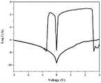
在真空条件下,蒸镀40-50nm的金,作为光电导器件的电极。如图2为PEA2PbBr4材料的光电导器件在405nm下的光电流与暗电流曲线。Under vacuum conditions, 40-50 nm gold was evaporated to serve as the electrode of the photoconductive device. Figure 2 shows the photocurrent and dark current curves of the photoconductive device of PEA2 PbBr4 material at 405 nm.
实施例2:Example 2:
本发明通过控制不同比例的前驱体,得到不同二维PEA2PbX4纳米片的紫外吸收曲线,具体步骤如下-The present invention obtains the ultraviolet absorption curves of different two-dimensional PEA2 PbX4 nanosheets by controlling different proportions of precursors, and the specific steps are as follows:
(1)称取PEABr与PbBr2以摩尔比为2:1混合,溶解于N,N-二甲基甲酰胺中,N,N-二甲基甲酰胺的体积mL与PEABr和PbBr2的之和摩尔量mmol的比值为3:5,在搅拌条件下加热,再过滤,得到(PEA)2PbBr4的前驱体溶液;取PEACl 0.4mmol,PbCl20.2mmol,摩尔比为2:1混合。以相同的步骤,得到(PEA)2PbCl4的前驱体溶液;取PEABr 0.2mmol,PEACl,0.2mmolPbCl2(1) Weigh and mix PEABr and PbBr2 with a molar ratio of 2:1, dissolve in N,N-dimethylformamide, the volume mL of N,N-dimethylformamide and the ratio of PEABr and PbBr2 The ratio to the molar amount of mmol is 3:5, heated under stirring conditions, and filtered again to obtain a precursor solution of (PEA)2 PbBr4 ; take PEACl 0.4 mmol, PbCl2 0.2 mmol, and mix at a molar ratio of 2:1. With the same steps, the precursor solution of (PEA)2 PbCl4 was obtained; take PEABr 0.2mmol, PEACl, 0.2mmolPbCl2
0.2mmol,摩尔比为1:1:1混合。以相同的步骤,得到(PEA)2PbCl3Br的前驱体溶液。0.2 mmol, the molar ratio is 1:1:1 mixed. Following the same procedure, a precursor solution of (PEA)2 PbCl3 Br was obtained.
(2)控制温度为室温,在1000-2000rpm强烈搅拌的条件下滴加上述步骤(1)得到的前驱体溶液至甲苯中,前驱体溶液与甲苯的体积比为2-4:1000-3000,通过反溶剂沉淀法获得分散在甲苯中的PEA2PbX4NPs纳米片,作为分散液;分散液做紫外-可见光吸收光谱测试,如图3,纳米片具有一个明亮,半高宽小于50nm的窄带吸收,(PEA)2PbCl4、(PEA)2PbCl3Br和(PEA)2PbBr4在可见光和近红外区域无吸收,在紫外波段340nm、355nm、405nm有强吸收。(2) the control temperature is room temperature, and the precursor solution obtained in the above step (1) is added dropwise to toluene under the condition of intense stirring at 1000-2000rpm, and the volume ratio of the precursor solution to toluene is 2-4:1000-3000, The PEA2 PbX4 NPs nanosheets dispersed in toluene were obtained by anti-solvent precipitation as a dispersion; the dispersion was tested by UV-Vis absorption spectrum, as shown in Figure 3, the nanosheets have a bright narrow band with a half width less than 50nm Absorption, (PEA)2 PbCl4 , (PEA)2 PbCl3 Br and (PEA)2 PbBr4 have no absorption in the visible and near-infrared regions, but have strong absorption in the ultraviolet bands at 340 nm, 355 nm, and 405 nm.
(3)取两块硅片衬底,分别依次采用乙醇、丙酮、乙醇清洗,再用紫外光处理10-30min,吹干,用刀刮开一端表面上的二氧化硅作为电极并连接导电线,其余部分浸没于上述步骤(2)获得的分散液中,施加电压60V,5min,获得二维的PEA2PbBr4纳米片。如图4为二维PEA2PbBr4的单片SEM图谱,如图5为二维PEA2PbBr4的SEM图谱。(3) Take two silicon wafer substrates, wash them with ethanol, acetone, and ethanol in turn, then treat them with ultraviolet light for 10-30min, blow dry, scrape off the silicon dioxide on one end surface with a knife as electrodes and connect conductive wires , and the remaining part was immersed in the dispersion obtained in the above step (2), and a voltage of 60 V was applied for 5 min to obtain two-dimensional PEA2 PbBr4 nanosheets. FIG. 4 is the single-sheet SEM pattern of the two-dimensional PEA2 PbBr4 , and FIG. 5 is the SEM pattern of the two-dimensional PEA2 PbBr4 .
Claims (10)
Priority Applications (2)
| Application Number | Priority Date | Filing Date | Title |
|---|---|---|---|
| CN202210211541.3ACN114685555B (en) | 2022-03-04 | 2022-03-04 | Two-dimensional (PEA) 2 PbX 4 Nanosheets, preparation method and application of nanosheets in ultraviolet light detector |
| PCT/CN2022/142908WO2023165243A1 (en) | 2022-03-04 | 2022-12-28 | Two-dimensional (pea)2pbx4 nanosheet, preparation method therefor, and use thereof in ultraviolet detector |
Applications Claiming Priority (1)
| Application Number | Priority Date | Filing Date | Title |
|---|---|---|---|
| CN202210211541.3ACN114685555B (en) | 2022-03-04 | 2022-03-04 | Two-dimensional (PEA) 2 PbX 4 Nanosheets, preparation method and application of nanosheets in ultraviolet light detector |
Publications (2)
| Publication Number | Publication Date |
|---|---|
| CN114685555Atrue CN114685555A (en) | 2022-07-01 |
| CN114685555B CN114685555B (en) | 2024-01-05 |
Family
ID=82136563
Family Applications (1)
| Application Number | Title | Priority Date | Filing Date |
|---|---|---|---|
| CN202210211541.3AActiveCN114685555B (en) | 2022-03-04 | 2022-03-04 | Two-dimensional (PEA) 2 PbX 4 Nanosheets, preparation method and application of nanosheets in ultraviolet light detector |
Country Status (2)
| Country | Link |
|---|---|
| CN (1) | CN114685555B (en) |
| WO (1) | WO2023165243A1 (en) |
Cited By (1)
| Publication number | Priority date | Publication date | Assignee | Title |
|---|---|---|---|---|
| WO2023165243A1 (en)* | 2022-03-04 | 2023-09-07 | 中国科学院深圳先进技术研究院 | Two-dimensional (pea)2pbx4 nanosheet, preparation method therefor, and use thereof in ultraviolet detector |
Family Cites Families (5)
| Publication number | Priority date | Publication date | Assignee | Title |
|---|---|---|---|---|
| WO2020049499A1 (en)* | 2018-09-06 | 2020-03-12 | King Abdullah University Of Science And Technology | Method for making inorganic perovskite nanocrystals film and applications |
| CN111192960B (en)* | 2018-11-14 | 2022-12-02 | 苏州大学 | A kind of ultraviolet-visible light dual-band photodetection device and its preparation method |
| CN110931642A (en)* | 2019-11-29 | 2020-03-27 | 南昌大学 | Ultraviolet light detector of two-dimensional perovskite single crystal and preparation method thereof |
| CN113257932B (en)* | 2021-05-12 | 2022-11-22 | 常熟理工学院 | High-performance photoelectric detector and preparation method thereof |
| CN114685555B (en)* | 2022-03-04 | 2024-01-05 | 中国科学院深圳先进技术研究院 | Two-dimensional (PEA) 2 PbX 4 Nanosheets, preparation method and application of nanosheets in ultraviolet light detector |
- 2022
- 2022-03-04CNCN202210211541.3Apatent/CN114685555B/enactiveActive
- 2022-12-28WOPCT/CN2022/142908patent/WO2023165243A1/ennot_activeCeased
Non-Patent Citations (1)
| Title |
|---|
| SHUANG YANG ET AL.: "Ultrathin Two-Dimensional Organic-Inorganic Hybrid Perovskite Nanosheets with Bright, Tunable Photoluminescence and High Stability", ANGEW. CHEM. INT. ED., vol. 56, pages 4252 - 4255* |
Cited By (1)
| Publication number | Priority date | Publication date | Assignee | Title |
|---|---|---|---|---|
| WO2023165243A1 (en)* | 2022-03-04 | 2023-09-07 | 中国科学院深圳先进技术研究院 | Two-dimensional (pea)2pbx4 nanosheet, preparation method therefor, and use thereof in ultraviolet detector |
Also Published As
| Publication number | Publication date |
|---|---|
| CN114685555B (en) | 2024-01-05 |
| WO2023165243A1 (en) | 2023-09-07 |
Similar Documents
| Publication | Publication Date | Title |
|---|---|---|
| CN109638091B (en) | Construction method and regulation and control strategy of high-performance hybrid photoelectric detector | |
| Yanhong et al. | A study of quantum confinement properties of photogenerated charges in ZnO nanoparticles by surface photovoltage spectroscopy | |
| Zhu et al. | Direct conversion of perovskite thin films into nanowires with kinetic control for flexible optoelectronic devices | |
| Zhu et al. | Antisolvent‐induced fastly grown all‐inorganic perovskite CsPbCl3 microcrystal films for high‐sensitive UV photodetectors | |
| CN109817812B (en) | Large particle perovskite single crystal/polymer composite thick film, photodetector and preparation method | |
| Khayatian et al. | Diameter-controlled synthesis of ZnO nanorods on Fe-doped ZnO seed layer and enhanced photodetection performance | |
| CN105609588B (en) | Au nanoparticle enhanced high-performance inorganic perovskite CsPbX3 nanocrystalline visible light detector | |
| CN105633189A (en) | Liquid-phase synthesized ultrathin inorganic perovskite CsPbBr3 nanosheet visible light detector | |
| CN113150785B (en) | A kind of CdSe quantum dot, its preparation method and photoconductive diode | |
| CN111525036B (en) | Self-driven perovskite photoelectric detector and preparation method thereof | |
| Raj et al. | Development of a highly sensitive UV sensor using Al, Ga, and In-doped NiO thin films via nebulizer spray pyrolysis method for photodetector applications | |
| CN111864080A (en) | A two-dimensional organic-inorganic hybrid perovskite crystal photodetector and preparation method thereof | |
| Khalef et al. | Photo detector fabrication based ZnO nanostructure on silicon substrate | |
| CN114685555B (en) | Two-dimensional (PEA) 2 PbX 4 Nanosheets, preparation method and application of nanosheets in ultraviolet light detector | |
| CN104638034B (en) | A kind of flexible thin-film solar cell | |
| Darman et al. | Pinhole-free 2D Ruddlesden–Popper perovskite layer with close packed large crystalline grains, suitable for optoelectronic applications | |
| CN106449978A (en) | Preparation method of visible blind ultraviolet detector based on CH3NH3PbCl3 film | |
| CN107123699B (en) | A kind of near infrared photodetector of driving certainly and preparation method thereof based on copper potassium sulfate quasi-one dimensional nanostructure | |
| CN114316947A (en) | Large-size lead sulfide quantum dot, quantum dot ink, printed solar cell and preparation method | |
| Shan et al. | Oil–water interfacial self-assembly of PS/ZnS nanospheres and photoconducting property of corresponding nanofilm | |
| CN116577382A (en) | A gas sensor based on light excitation, its preparation method and application | |
| CN103048043B (en) | Based on light or the gas detector of inorganic semiconductor monocrystalline network structure | |
| Peng et al. | UV–Vis photodetector based on ionic liquid-modified perovskite–ZnO composite | |
| CN112909109B (en) | A Self-Powered Nanoscale Ultraviolet Detector Based on Laterally Bridged Pn Junction | |
| CN114597317A (en) | UV-Vis light detector based on β-Ga2O3/Au/MAPbBr3 sandwich structure and preparation method |
Legal Events
| Date | Code | Title | Description |
|---|---|---|---|
| PB01 | Publication | ||
| PB01 | Publication | ||
| SE01 | Entry into force of request for substantive examination | ||
| SE01 | Entry into force of request for substantive examination | ||
| GR01 | Patent grant | ||
| GR01 | Patent grant |