CN114678334A - A narrow border display panel and display device - Google Patents
A narrow border display panel and display deviceDownload PDFInfo
- Publication number
- CN114678334A CN114678334ACN202210308675.7ACN202210308675ACN114678334ACN 114678334 ACN114678334 ACN 114678334ACN 202210308675 ACN202210308675 ACN 202210308675ACN 114678334 ACN114678334 ACN 114678334A
- Authority
- CN
- China
- Prior art keywords
- display area
- layer
- adhesive layer
- heat dissipation
- display
- Prior art date
- Legal status (The legal status is an assumption and is not a legal conclusion. Google has not performed a legal analysis and makes no representation as to the accuracy of the status listed.)
- Granted
Links
Images


Classifications
- H—ELECTRICITY
- H01—ELECTRIC ELEMENTS
- H01L—SEMICONDUCTOR DEVICES NOT COVERED BY CLASS H10
- H01L23/00—Details of semiconductor or other solid state devices
- H01L23/34—Arrangements for cooling, heating, ventilating or temperature compensation ; Temperature sensing arrangements
- H01L23/36—Selection of materials, or shaping, to facilitate cooling or heating, e.g. heatsinks
- H01L23/367—Cooling facilitated by shape of device
- G—PHYSICS
- G09—EDUCATION; CRYPTOGRAPHY; DISPLAY; ADVERTISING; SEALS
- G09F—DISPLAYING; ADVERTISING; SIGNS; LABELS OR NAME-PLATES; SEALS
- G09F9/00—Indicating arrangements for variable information in which the information is built-up on a support by selection or combination of individual elements
- G09F9/30—Indicating arrangements for variable information in which the information is built-up on a support by selection or combination of individual elements in which the desired character or characters are formed by combining individual elements
- G09F9/301—Indicating arrangements for variable information in which the information is built-up on a support by selection or combination of individual elements in which the desired character or characters are formed by combining individual elements flexible foldable or roll-able electronic displays, e.g. thin LCD, OLED
- H—ELECTRICITY
- H01—ELECTRIC ELEMENTS
- H01L—SEMICONDUCTOR DEVICES NOT COVERED BY CLASS H10
- H01L23/00—Details of semiconductor or other solid state devices
- H01L23/34—Arrangements for cooling, heating, ventilating or temperature compensation ; Temperature sensing arrangements
- H01L23/36—Selection of materials, or shaping, to facilitate cooling or heating, e.g. heatsinks
- H01L23/373—Cooling facilitated by selection of materials for the device or materials for thermal expansion adaptation, e.g. carbon
- H01L23/3735—Laminates or multilayers, e.g. direct bond copper ceramic substrates
- H—ELECTRICITY
- H01—ELECTRIC ELEMENTS
- H01L—SEMICONDUCTOR DEVICES NOT COVERED BY CLASS H10
- H01L23/00—Details of semiconductor or other solid state devices
- H01L23/34—Arrangements for cooling, heating, ventilating or temperature compensation ; Temperature sensing arrangements
- H01L23/36—Selection of materials, or shaping, to facilitate cooling or heating, e.g. heatsinks
- H01L23/373—Cooling facilitated by selection of materials for the device or materials for thermal expansion adaptation, e.g. carbon
- H01L23/3736—Metallic materials
- H—ELECTRICITY
- H01—ELECTRIC ELEMENTS
- H01L—SEMICONDUCTOR DEVICES NOT COVERED BY CLASS H10
- H01L23/00—Details of semiconductor or other solid state devices
- H01L23/34—Arrangements for cooling, heating, ventilating or temperature compensation ; Temperature sensing arrangements
- H01L23/36—Selection of materials, or shaping, to facilitate cooling or heating, e.g. heatsinks
- H01L23/373—Cooling facilitated by selection of materials for the device or materials for thermal expansion adaptation, e.g. carbon
- H01L23/3738—Semiconductor materials
- H—ELECTRICITY
- H01—ELECTRIC ELEMENTS
- H01L—SEMICONDUCTOR DEVICES NOT COVERED BY CLASS H10
- H01L25/00—Assemblies consisting of a plurality of semiconductor or other solid state devices
- H01L25/18—Assemblies consisting of a plurality of semiconductor or other solid state devices the devices being of the types provided for in two or more different main groups of the same subclass of H10B, H10D, H10F, H10H, H10K or H10N
Landscapes
- Engineering & Computer Science (AREA)
- Chemical & Material Sciences (AREA)
- Materials Engineering (AREA)
- Physics & Mathematics (AREA)
- General Physics & Mathematics (AREA)
- Microelectronics & Electronic Packaging (AREA)
- Condensed Matter Physics & Semiconductors (AREA)
- Computer Hardware Design (AREA)
- Power Engineering (AREA)
- Ceramic Engineering (AREA)
- Theoretical Computer Science (AREA)
- Devices For Indicating Variable Information By Combining Individual Elements (AREA)
Abstract
Translated fromChinese
Description
Translated fromChinese技术领域technical field
本公开涉及显示领域,特别涉及一种窄边框显示面板及显示设备。The present disclosure relates to the field of display, and in particular, to a narrow-frame display panel and a display device.
背景技术Background technique
随着手机等电子产品的全屏显示以及大屏显示效果越来越受到用户青睐,显示模组的窄边框设计显得尤为重要。在现有技术方案中,实现下边框减窄的重要方法之一为减小弯折半径。然而,现有的叠层结构已经缩减到极致,但仍然较厚,无法与窄边框弯折半径匹配,无法实现窄边框效果。As the full-screen display and large-screen display effects of electronic products such as mobile phones are increasingly favored by users, the narrow frame design of display modules is particularly important. In the prior art solution, one of the important methods for realizing the narrowing of the lower frame is to reduce the bending radius. However, the existing laminated structure has been reduced to the extreme, but is still thick, cannot match the bending radius of the narrow frame, and cannot achieve the narrow frame effect.
发明内容SUMMARY OF THE INVENTION
有鉴于此,本公开实施例提出了一种窄边框显示面板及显示设备,用以解决现有技术的如下问题:现有的叠层结构已经缩减到极致,但仍然较厚,无法与窄边框弯折半径匹配,无法实现窄边框效果。In view of this, embodiments of the present disclosure propose a narrow-bezel display panel and a display device to solve the following problems in the prior art: the existing laminated structure has been reduced to the extreme, but is still thick and cannot be compared with the narrow bezel. The bending radius is matched, and the narrow border effect cannot be achieved.
一方面,本公开实施例提出了一种窄边框显示面板,至少包括:散热膜层、显示层、第一胶层、第二胶层;所述显示层包括显示区、弯折区、非显示区,所述显示区和所述非显示区通过所述弯折区连接,所述显示区和所述非显示区相互平行,所述非显示区的尺寸小于所述显示区的尺寸;所述散热膜层设置在所述显示区和所述非显示区之间,所述显示区通过第一胶层与所述散热膜层连接,所述非显示区通过第二胶层与所述散热膜层连接;所述散热膜层在所述非显示区到所述显示区的正投影范围内具有镂空结构,所述镂空结构内嵌入有部分所述第二胶层。On the one hand, an embodiment of the present disclosure provides a narrow-frame display panel, which at least includes: a heat dissipation film layer, a display layer, a first adhesive layer, and a second adhesive layer; the display layer includes a display area, a bending area, a non-display area The display area and the non-display area are connected by the bending area, the display area and the non-display area are parallel to each other, and the size of the non-display area is smaller than that of the display area; the The heat dissipation film layer is arranged between the display area and the non-display area, the display area is connected to the heat dissipation film layer through a first adhesive layer, and the non-display area is connected to the heat dissipation film through a second adhesive layer Layer connection; the heat dissipation film layer has a hollow structure in the orthographic projection range from the non-display area to the display area, and a part of the second adhesive layer is embedded in the hollow structure.
在一些实施例中,所述散热膜层为金属膜层。In some embodiments, the heat dissipation film layer is a metal film layer.
在一些实施例中,所述散热膜层包括:缓冲层和金属膜层,所述缓冲层与所述第一胶层连接,所述金属膜层与所述第二胶层连接,所述镂空结构设置在所述金属膜层上。In some embodiments, the heat dissipation film layer includes: a buffer layer and a metal film layer, the buffer layer is connected to the first adhesive layer, the metal film layer is connected to the second adhesive layer, and the hollow A structure is provided on the metal film layer.
在一些实施例中,所述第二胶层与所述散热膜层的连接面上设置有导热材料,或者,所述第二胶层的材料中掺杂有导热材料。In some embodiments, a thermally conductive material is provided on the connecting surface of the second adhesive layer and the heat dissipation film layer, or the material of the second adhesive layer is doped with a thermally conductive material.
在一些实施例中,所述导热材料至少包括以下之一:石墨、石墨烯。In some embodiments, the thermally conductive material includes at least one of the following: graphite and graphene.
在一些实施例中,所述镂空结构的图案至少包括以下之一:长方形、正方形、圆形、三角形。In some embodiments, the pattern of the hollow structure includes at least one of the following: rectangle, square, circle, and triangle.
在一些实施例中,所述第一胶层与所述显示区的连接面上具有网格状结构。In some embodiments, the connection surface between the first adhesive layer and the display area has a grid-like structure.
在一些实施例中,所述第一胶层的材料与第二胶层的材料不同。In some embodiments, the material of the first adhesive layer is different from the material of the second adhesive layer.
在一些实施例中,还包括:驱动芯片,设置在所述非显示区上,通过所述非显示区与所述散热膜层连接。In some embodiments, it further includes: a driving chip, disposed on the non-display area, and connected to the heat dissipation film layer through the non-display area.
另一方面,本公开实施例提出了一种显示设备,至少包括:本公开任一实施例所述的窄边框显示面板。On the other hand, an embodiment of the present disclosure provides a display device, which at least includes: the narrow-frame display panel described in any embodiment of the present disclosure.
本公开实施例在散热膜层上设置了镂空结构,镂空结构仅位于非显示区到显示区的正投影范围内,镂空结构的所在区域的面积较小,仅与非显示区对应,不会影响散热膜层的原有散热性能,但镂空结构的镂空部分可以渗入涂覆的第二胶层,当第二胶层涂覆的厚度不变时,部分第二胶层内嵌至镂空结构中,导致第二胶层在散热膜层上的厚度变薄,但嵌入镂空结构中的部分第二胶层仍然具有粘结力,在不影响第二胶层粘结力的同时减薄了显示区与非显示区之间的厚度,进而使得弯折半径变小。本公开实施例通过调整镂空结构的镂空量多少来调整第二胶层在散热膜层上的厚度,使得弯折半径可以与窄边框弯折半径匹配,实现窄边框效果。In the embodiment of the present disclosure, a hollow structure is arranged on the heat dissipation film layer. The hollow structure is only located in the orthographic projection range from the non-display area to the display area. The area where the hollow structure is located is small and only corresponds to the non-display area and will not affect the The original heat dissipation performance of the heat dissipation film layer, but the hollow part of the hollow structure can penetrate into the coated second adhesive layer. When the coating thickness of the second adhesive layer remains unchanged, part of the second adhesive layer is embedded in the hollow structure. As a result, the thickness of the second adhesive layer on the heat dissipation film layer becomes thinner, but part of the second adhesive layer embedded in the hollow structure still has adhesive force, which reduces the thickness of the display area and the The thickness between the non-display areas makes the bending radius smaller. In the embodiment of the present disclosure, the thickness of the second adhesive layer on the heat dissipation film layer is adjusted by adjusting the amount of the hollow structure, so that the bending radius can match the bending radius of the narrow frame, thereby realizing the narrow frame effect.
附图说明Description of drawings
为了更清楚地说明本公开实施例或现有技术中的技术方案,下面将对实施例或现有技术描述中所需要使用的附图作简单地介绍,显而易见地,下面描述中的附图仅仅是本公开中记载的一些实施例,对于本领域普通技术人员来讲,在不付出创造性劳动性的前提下,还可以根据这些附图获得其他的附图。In order to more clearly illustrate the embodiments of the present disclosure or the technical solutions in the prior art, the following briefly introduces the accompanying drawings that need to be used in the description of the embodiments or the prior art. Obviously, the drawings in the following description are only These are some embodiments described in the present disclosure. For those of ordinary skill in the art, other drawings can also be obtained according to these drawings without any creative effort.
图1为现有技术提供的显示模组弯折半径的示意图;1 is a schematic diagram of a bending radius of a display module provided by the prior art;
图2为本公开第一实施例提供的窄边框显示面板的剖面结构示意图;FIG. 2 is a schematic cross-sectional structure diagram of a narrow-frame display panel according to a first embodiment of the present disclosure;
图3为本公开第二实施例提供的窄边框显示面板的剖面结构示意图;FIG. 3 is a schematic cross-sectional structure diagram of a narrow-frame display panel according to a second embodiment of the present disclosure;
图4为本公开第三实施例提供的窄边框显示面板的剖面结构示意图;4 is a schematic cross-sectional structural diagram of a narrow-frame display panel provided by a third embodiment of the present disclosure;
图5为本公开第三实施例提供的窄边框显示面板的叠层结构示意图;5 is a schematic diagram of a stacked structure of a narrow-frame display panel according to a third embodiment of the present disclosure;
图6为本公开第三实施例提供的窄边框显示面板导热金属层的正视图;6 is a front view of a thermally conductive metal layer of a narrow-frame display panel provided by a third embodiment of the present disclosure;
图7为本公开第三实施例提供的窄边框显示面板部分结构的模切工艺流程图。FIG. 7 is a flow chart of a die-cutting process for a partial structure of a narrow-frame display panel according to a third embodiment of the present disclosure.
附图标记:Reference number:
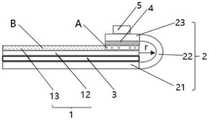
1-散热膜层,2-显示层,3-第一胶层,4-第二胶层,5-驱动芯片,11-镂空结构,12-缓冲层,13-金属膜层,21-显示区,22-弯折区,23-非显示区。1- heat dissipation film layer, 2- display layer, 3- first adhesive layer, 4- second adhesive layer, 5- driver chip, 11- hollow structure, 12- buffer layer, 13- metal film layer, 21- display area , 22-bending area, 23-non-display area.
具体实施方式Detailed ways
为了使得本公开实施例的目的、技术方案和优点更加清楚,下面将结合本公开实施例的附图,对本公开实施例的技术方案进行清楚、完整地描述。显然,所描述的实施例是本公开的一部分实施例,而不是全部的实施例。基于所描述的本公开的实施例,本领域普通技术人员在无需创造性劳动的前提下所获得的所有其他实施例,都属于本公开保护的范围。In order to make the purposes, technical solutions and advantages of the embodiments of the present disclosure more clear, the technical solutions of the embodiments of the present disclosure will be clearly and completely described below with reference to the accompanying drawings of the embodiments of the present disclosure. Obviously, the described embodiments are some, but not all, embodiments of the present disclosure. Based on the described embodiments of the present disclosure, all other embodiments obtained by those of ordinary skill in the art without creative efforts fall within the protection scope of the present disclosure.
除非另外定义,本公开使用的技术术语或者科学术语应当为本公开所属领域内具有一般技能的人士所理解的通常意义。本公开中使用的“第一”、“第二”以及类似的词语并不表示任何顺序、数量或者重要性,而只是用来区分不同的组成部分。“包括”或者“包含”等类似的词语意指出现该词前面的元件或者物件涵盖出现在该词后面列举的元件或者物件及其等同,而不排除其他元件或者物件。“连接”或者“相连”等类似的词语并非限定于物理的或者机械的连接,而是可以包括电性的连接,不管是直接的还是间接的。“上”、“下”、“左”、“右”等仅用于表示相对位置关系,当被描述对象的绝对位置改变后,则该相对位置关系也可能相应地改变。Unless otherwise defined, technical or scientific terms used in this disclosure shall have the ordinary meaning as understood by one of ordinary skill in the art to which this disclosure belongs. As used in this disclosure, "first," "second," and similar terms do not denote any order, quantity, or importance, but are merely used to distinguish the various components. "Comprises" or "comprising" and similar words mean that the elements or things appearing before the word encompass the elements or things recited after the word and their equivalents, but do not exclude other elements or things. Words like "connected" or "connected" are not limited to physical or mechanical connections, but may include electrical connections, whether direct or indirect. "Up", "Down", "Left", "Right", etc. are only used to represent the relative positional relationship, and when the absolute position of the described object changes, the relative positional relationship may also change accordingly.
为了保持本公开实施例的以下说明清楚且简明,本公开省略了已知功能和已知部件的详细说明。In order to keep the following description of the embodiments of the present disclosure clear and concise, the present disclosure omits detailed descriptions of well-known functions and well-known components.
图1中的弯折半径(r)是通过弯折区连接的显示区和非显示区之间的叠层厚度确定的,将图1中的弯折半径减到越小越好,然而,现有的叠层结构已经缩减到极致,几微米的厚度都无法缩减,无法与窄边框弯折半径匹配,进而无法实现窄边框效果。因此,如何在不影响现有性能基础上,实现弯折区域叠层的厚度减小是本公开实施例主要解决的问题。The bending radius (r) in Figure 1 is determined by the thickness of the stack between the display area and the non-display area connected by the bending area, and the smaller the bending radius in Figure 1, the better, however, now Some laminated structures have been reduced to the extreme, and the thickness of several microns cannot be reduced, which cannot match the bending radius of the narrow frame, so that the narrow frame effect cannot be achieved. Therefore, how to reduce the thickness of the stack in the bending region without affecting the existing performance is the main problem to be solved by the embodiments of the present disclosure.
实施例一Example 1
本公开第一实施例提供了一种窄边框显示面板,其剖面结构示意如图2所示,至少包括:The first embodiment of the present disclosure provides a narrow-frame display panel, the schematic cross-sectional structure of which is shown in FIG. 2 , and includes at least:
散热膜层1、显示层2、第一胶层3、第二胶层4;Heat
显示层2包括显示区21、弯折区22、非显示区23,显示区和非显示区通过弯折区连接,显示区和非显示区相互平行,非显示区的尺寸小于显示区的尺寸;The
散热膜层1设置在显示区21和非显示区23之间,显示区21通过第一胶层3与散热膜层1连接,非显示区23通过第二胶层4与散热膜层1连接;散热膜层1在非显示区23到显示区21的正投影范围内具有镂空结构11,镂空结构11内嵌入有部分第二胶层4。The heat
上述剖面图仅为一个剖面,在正视方向,散热膜层的尺寸与显示区的尺寸相同。在正视方向上,上述镂空结构的图案可以为长方形、正方形、圆形、三角形等各种图案,本公开实施例不进行限定。对于加工上述镂空结构的图案的工艺,其可以采用模切工艺、蚀刻工艺、激光切割工艺等任何可以实现的工艺,此处也不进行限定。The above cross-sectional view is only a cross-section, and in the front view, the size of the heat dissipation film layer is the same as that of the display area. In the front view direction, the pattern of the hollow structure can be various patterns such as rectangle, square, circle, triangle, etc., which is not limited in the embodiment of the present disclosure. For the process of processing the pattern of the hollow structure, any achievable process such as die cutting process, etching process, laser cutting process, etc. may be used, which is not limited here.
在优选实施例中,由于第一胶层和第二胶层所粘结的材料不同,所以第一胶层的材料可以与第二胶层的材料不同,例如,第二胶层可以为丙烯酸类型的胶,而第一胶层可以为剥离力更大一些的亚克力类型的胶。In a preferred embodiment, since the materials to which the first adhesive layer and the second adhesive layer are bonded are different, the material of the first adhesive layer may be different from that of the second adhesive layer, for example, the second adhesive layer may be of acrylic type adhesive, and the first adhesive layer can be an acrylic adhesive with a stronger peeling force.
由于第一胶层和第二胶层所粘结的材料不同,第一胶层的一面是与显示区粘结的,因此,为了保护显示区,让第一胶层更好的贴附在显示区,优选在第一胶层与显示区的连接面上设置网格状结构。Because the materials to which the first adhesive layer and the second adhesive layer are bonded are different, one side of the first adhesive layer is bonded to the display area. Therefore, in order to protect the display area, the first adhesive layer can be better attached to the display area. Preferably, a grid-like structure is arranged on the connecting surface of the first adhesive layer and the display area.
本公开实施例在散热膜层上设置了镂空结构,镂空结构仅位于非显示区到显示区的正投影范围内,镂空结构的所在区域的面积较小,仅与非显示区对应,不会影响散热膜层的原有散热性能,但镂空结构的镂空部分可以渗入涂覆的第二胶层,当第二胶层涂覆的厚度不变时,部分第二胶层内嵌至镂空结构中,导致第二胶层在散热膜层上的厚度变薄,但嵌入镂空结构中的部分第二胶层仍然具有粘结力,在不影响第二胶层粘结力的同时减薄了显示区与非显示区之间的厚度,进而使得弯折半径变小。例如,涂覆第二胶层的厚度为50um,现有技术中将第二胶层压接后的厚度为40um,但采用本公开实施例后,在压接时部分第二胶层渗入到镂空结构中,在第二胶层成为固态后,第二胶层在散热膜层上的厚度变为30um,相对于现有技术而言,大大减薄了第二胶层的厚度。In the embodiment of the present disclosure, a hollow structure is arranged on the heat dissipation film layer. The hollow structure is only located in the orthographic projection range from the non-display area to the display area. The area where the hollow structure is located is small and only corresponds to the non-display area and will not affect the The original heat dissipation performance of the heat dissipation film layer, but the hollow part of the hollow structure can penetrate into the coated second adhesive layer. When the coating thickness of the second adhesive layer remains unchanged, part of the second adhesive layer is embedded in the hollow structure. As a result, the thickness of the second adhesive layer on the heat dissipation film layer becomes thinner, but part of the second adhesive layer embedded in the hollow structure still has adhesive force, which reduces the thickness of the display area and the The thickness between the non-display areas makes the bending radius smaller. For example, the thickness of the second adhesive layer is 50um. In the prior art, the thickness of the second adhesive layer after lamination is 40um. However, after using the embodiment of the present disclosure, part of the second adhesive layer penetrates into the hollow during crimping. In the structure, after the second adhesive layer becomes solid, the thickness of the second adhesive layer on the heat dissipation film layer becomes 30um, which greatly reduces the thickness of the second adhesive layer compared to the prior art.
本公开实施例通过调整镂空结构的镂空量多少来调整第二胶层在散热膜层上的厚度,使得弯折半径可以与窄边框弯折半径匹配,实现窄边框效果。In the embodiment of the present disclosure, the thickness of the second adhesive layer on the heat dissipation film layer is adjusted by adjusting the amount of the hollow structure, so that the bending radius can match the bending radius of the narrow frame, thereby realizing the narrow frame effect.
实施例二
本公开第二实施例提供了一种窄边框显示面板,其剖面结构示意如图3所示,至少包括:A second embodiment of the present disclosure provides a narrow-frame display panel, the schematic cross-sectional structure of which is shown in FIG. 3 , and includes at least:
散热膜层1、显示层2、第一胶层3、第二胶层4;Heat
显示层2包括显示区21、弯折区22、非显示区23,显示区和非显示区通过弯折区连接,显示区和非显示区相互平行,非显示区的尺寸小于显示区的尺寸;The
散热膜层1设置在显示区21和非显示区23之间,显示区21通过第一胶层3与散热膜层1连接,非显示区23通过第二胶层4与散热膜层1连接;散热膜层1在非显示区23到显示区21的正投影范围内具有镂空结构11,镂空结构11内嵌入有部分第二胶层4;The heat
其中,散热膜层1包括:缓冲层12和金属膜层13,缓冲层与第一胶层连接,金属膜层与第二胶层连接,镂空结构设置在金属膜层上。The heat
本公开实施例的散热膜层为包括缓冲层和技术膜层两层的一个结构,缓冲层优选可以设置为泡棉。具体实现时,设置上述缓冲层仅为一种优选实施方式,缓冲层可以减少金属膜层的热量对显示区带来的高温风险,当然,散热膜层也可以仅包括金属膜层,但其在具体实现时,可能会对显示区的像素构成一定风险,因此,优选设置缓冲层。The heat dissipation film layer in the embodiment of the present disclosure is a structure including a buffer layer and a technical film layer, and the buffer layer can preferably be configured as foam. In specific implementation, the provision of the above buffer layer is only a preferred embodiment. The buffer layer can reduce the risk of high temperature caused by the heat of the metal film layer to the display area. Of course, the heat dissipation film layer can also only include the metal film layer, but its During specific implementation, certain risks may be posed to the pixels in the display area, therefore, a buffer layer is preferably provided.
上述剖面图仅为一个剖面,在正视方向,散热膜层的尺寸与显示区的尺寸相同。在正视方向上,上述镂空结构的图案可以为长方形、正方形、圆形、三角形等各种图案,本公开实施例不进行限定。对于加工上述镂空结构的图案的工艺,其可以采用模切工艺、蚀刻工艺、激光切割工艺等任何可以实现的工艺,此处也不进行限定。The above cross-sectional view is only a cross-section, and in the front view, the size of the heat dissipation film layer is the same as that of the display area. In the front view direction, the pattern of the hollow structure can be various patterns such as rectangle, square, circle, triangle, etc., which is not limited in the embodiment of the present disclosure. For the process of processing the pattern of the hollow structure, any achievable process such as die cutting process, etching process, laser cutting process, etc. may be used, which is not limited here.
在优选实施例中,由于第一胶层和第二胶层所粘结的材料不同,所以第一胶层的材料可以与第二胶层的材料不同,例如,第二胶层可以为丙烯酸类型的胶,而第一胶层可以为剥离力更大一些的亚克力类型的胶。In a preferred embodiment, since the materials to which the first adhesive layer and the second adhesive layer are bonded are different, the material of the first adhesive layer may be different from that of the second adhesive layer, for example, the second adhesive layer may be of acrylic type adhesive, and the first adhesive layer can be an acrylic adhesive with a stronger peeling force.
由于第一胶层和第二胶层所粘结的材料不同,第一胶层的一面是与显示区粘结的,因此,为了保护显示区,让第一胶层更好的贴附在显示区,优选在第一胶层与显示区的连接面上设置网格状结构。Because the materials to which the first adhesive layer and the second adhesive layer are bonded are different, one side of the first adhesive layer is bonded to the display area. Therefore, in order to protect the display area, the first adhesive layer can be better attached to the display area. Preferably, a grid-like structure is arranged on the connecting surface of the first adhesive layer and the display area.
本公开实施例在散热膜层上设置了镂空结构,镂空结构仅位于非显示区到显示区的正投影范围内,镂空结构的所在区域的面积较小,仅与非显示区对应,不会影响散热膜层的原有散热性能,但镂空结构的镂空部分可以渗入涂覆的第二胶层,当第二胶层涂覆的厚度不变时,部分第二胶层内嵌至镂空结构中,导致第二胶层在散热膜层上的厚度变薄,但嵌入镂空结构中的部分第二胶层仍然具有粘结力,在不影响第二胶层粘结力的同时减薄了显示区与非显示区之间的厚度,进而使得弯折半径变小。例如,涂覆第二胶层的厚度为50um,现有技术中将第二胶层压接后的厚度为45um,但采用本公开实施例后,在压接时部分第二胶层渗入到镂空结构中,在第二胶层成为固态后,第二胶层在散热膜层上的厚度变为30um,相对于现有技术而言,大大减薄了第二胶层的厚度。In the embodiment of the present disclosure, a hollow structure is arranged on the heat dissipation film layer. The hollow structure is only located in the orthographic projection range from the non-display area to the display area. The area where the hollow structure is located is small and only corresponds to the non-display area and will not affect the The original heat dissipation performance of the heat dissipation film layer, but the hollow part of the hollow structure can penetrate into the coated second adhesive layer. When the coating thickness of the second adhesive layer remains unchanged, part of the second adhesive layer is embedded in the hollow structure. As a result, the thickness of the second adhesive layer on the heat dissipation film layer becomes thinner, but part of the second adhesive layer embedded in the hollow structure still has adhesive force, which reduces the thickness of the display area and the The thickness between the non-display areas makes the bending radius smaller. For example, the thickness of the second adhesive layer is 50um. In the prior art, the thickness of the second adhesive layer after lamination is 45um. However, after using the embodiment of the present disclosure, part of the second adhesive layer penetrates into the hollow during crimping. In the structure, after the second adhesive layer becomes solid, the thickness of the second adhesive layer on the heat dissipation film layer becomes 30um, which greatly reduces the thickness of the second adhesive layer compared to the prior art.
本公开实施例通过调整镂空结构的镂空量多少来调整第二胶层在散热膜层上的厚度,使得弯折半径可以与窄边框弯折半径匹配,实现窄边框效果。In the embodiment of the present disclosure, the thickness of the second adhesive layer on the heat dissipation film layer is adjusted by adjusting the amount of the hollow structure, so that the bending radius can match the bending radius of the narrow frame, thereby realizing the narrow frame effect.
实施例三
本公开第三实施例提供了一种窄边框显示面板,其剖面结构示意如图4所示,至少包括:A third embodiment of the present disclosure provides a narrow-frame display panel, the schematic cross-sectional structure of which is shown in FIG. 4 , and includes at least:
散热膜层1、显示层2、第一胶层3、第二胶层4、驱动芯片5;Heat
显示层2包括显示区21、弯折区22、非显示区23,显示区和非显示区通过弯折区连接,显示区和非显示区相互平行,非显示区的尺寸小于显示区的尺寸;The
散热膜层1设置在显示区21和非显示区23之间,显示区21通过第一胶层3与散热膜层1连接,非显示区23通过第二胶层4与散热膜层1连接;散热膜层1在非显示区23到显示区21的正投影范围内具有镂空结构11,镂空结构11内嵌入有部分第二胶层4;驱动芯片5设置在非显示区上,通过非显示区与散热膜层连接;The heat
其中,散热膜层1包括:缓冲层12和金属膜层13,缓冲层与第一胶层连接,金属膜层与第二胶层连接,镂空结构设置在金属膜层上;Wherein, the heat
第二胶层与散热膜层的连接面上设置有导热材料,或者,第二胶层的材料中掺杂有导热材料。A thermally conductive material is provided on the connecting surface of the second adhesive layer and the heat dissipation film layer, or the material of the second adhesive layer is doped with a thermally conductive material.
本公开实施例的散热膜层为包括缓冲层和技术膜层两层的一个结构,缓冲层优选可以设置为泡棉。具体实现时,设置上述缓冲层仅为一种优选实施方式,缓冲层可以减少金属膜层的热量对显示区带来的高温风险,当然,散热膜层也可以仅包括金属膜层,但其在具体实现时,可能会对显示区的像素构成一定风险,因此,优选设置缓冲层。The heat dissipation film layer in the embodiment of the present disclosure is a structure including a buffer layer and a technical film layer, and the buffer layer can preferably be configured as foam. In specific implementation, the provision of the above buffer layer is only a preferred embodiment. The buffer layer can reduce the risk of high temperature caused by the heat of the metal film layer to the display area. Of course, the heat dissipation film layer can also only include the metal film layer, but its During specific implementation, certain risks may be posed to the pixels in the display area, therefore, a buffer layer is preferably provided.
本公开实施例由于在散热膜层上(与非显示区对应的部分)设置了镂空结构,散热膜层为金属膜层,其散热效果相对于没有镂空结构时而言,导热性能会变差,且镂空结构与非显示区对应,非显示区上又设置有驱动芯片,驱动芯片工作又会产生较多热量,因此,本公开实施例增加了导热材料来辅助导热。在不影响第二胶层粘结力的情况下,可以在第二胶层的材料中掺杂导热材料,但为了能够更好的辅助导热且不破坏第二胶层的粘结力,优选在第二胶层与散热膜层的连接面上设置导热材料。对于导热材料,其可以是石墨、石墨烯等物质,此处不进行一一举例。In the embodiment of the present disclosure, since a hollow structure is provided on the heat dissipation film layer (the part corresponding to the non-display area), and the heat dissipation film layer is a metal film layer, the heat dissipation effect of the heat dissipation film layer is worse than that without the hollow structure. The hollow structure corresponds to the non-display area, and the non-display area is provided with a driving chip, and the operation of the driving chip will generate more heat. Therefore, in the embodiment of the present disclosure, a thermally conductive material is added to assist heat conduction. Without affecting the adhesive force of the second adhesive layer, a thermally conductive material can be doped into the material of the second adhesive layer, but in order to better assist heat conduction without destroying the adhesive force of the second adhesive layer, it is preferable to A heat-conducting material is arranged on the connecting surface of the second adhesive layer and the heat-dissipating film layer. For the thermally conductive material, it can be materials such as graphite, graphene, etc., which are not listed here.
上述剖面图仅为一个剖面,在正视方向,散热膜层的尺寸与显示区的尺寸相同。在正视方向上,上述镂空结构的图案可以为长方形、正方形、圆形、三角形等各种图案,本公开实施例不进行限定。对于加工上述镂空结构的图案的工艺,其可以采用模切工艺、蚀刻工艺、激光切割工艺等任何可以实现的工艺,此处也不进行限定。The above cross-sectional view is only a cross-section, and in the front view, the size of the heat dissipation film layer is the same as that of the display area. In the front view direction, the pattern of the hollow structure can be various patterns such as rectangle, square, circle, triangle, etc., which is not limited in the embodiment of the present disclosure. For the process of processing the pattern of the hollow structure, any achievable process such as die cutting process, etching process, laser cutting process, etc. may be used, which is not limited here.
在优选实施例中,由于第一胶层和第二胶层所粘结的材料不同,所以第一胶层的材料可以与第二胶层的材料不同,例如,第二胶层可以为丙烯酸类型的胶,而第一胶层可以为剥离力更大一些的亚克力类型的胶。In a preferred embodiment, since the materials to which the first adhesive layer and the second adhesive layer are bonded are different, the material of the first adhesive layer may be different from that of the second adhesive layer, for example, the second adhesive layer may be of acrylic type adhesive, and the first adhesive layer can be an acrylic adhesive with a stronger peeling force.
由于第一胶层和第二胶层所粘结的材料不同,第一胶层的一面是与显示区粘结的,因此,为了保护显示区,让第一胶层更好的贴附在显示区,优选在第一胶层与显示区的连接面上设置网格状结构。Because the materials to which the first adhesive layer and the second adhesive layer are bonded are different, one side of the first adhesive layer is bonded to the display area. Therefore, in order to protect the display area, the first adhesive layer can be better attached to the display area. Preferably, a grid-like structure is arranged on the connecting surface of the first adhesive layer and the display area.
本公开实施例在散热膜层上设置了镂空结构,镂空结构仅位于非显示区到显示区的正投影范围内,镂空结构的所在区域的面积较小,仅与非显示区对应,不会影响散热膜层的原有散热性能,但镂空结构的镂空部分可以渗入涂覆的第二胶层,当第二胶层涂覆的厚度不变时,部分第二胶层内嵌至镂空结构中,导致第二胶层在散热膜层上的厚度变薄,但嵌入镂空结构中的部分第二胶层仍然具有粘结力,在不影响第二胶层粘结力的同时减薄了显示区与非显示区之间的厚度,进而使得弯折半径变小。例如,涂覆第二胶层的厚度为50um,现有技术中将第二胶层压接后的厚度为45um,但采用本公开实施例后,在压接时部分第二胶层渗入到镂空结构中,在第二胶层成为固态后,第二胶层在散热膜层上的厚度变为35um,相对于现有技术而言,大大减薄了第二胶层的厚度。In the embodiment of the present disclosure, a hollow structure is arranged on the heat dissipation film layer. The hollow structure is only located in the orthographic projection range from the non-display area to the display area. The area where the hollow structure is located is small and only corresponds to the non-display area and will not affect the The original heat dissipation performance of the heat dissipation film layer, but the hollow part of the hollow structure can penetrate into the coated second adhesive layer. When the coating thickness of the second adhesive layer remains unchanged, part of the second adhesive layer is embedded in the hollow structure. As a result, the thickness of the second adhesive layer on the heat dissipation film layer becomes thinner, but part of the second adhesive layer embedded in the hollow structure still has adhesive force, which reduces the thickness of the display area and the The thickness between the non-display areas makes the bending radius smaller. For example, the thickness of the second adhesive layer is 50um. In the prior art, the thickness of the second adhesive layer after lamination is 45um. However, after using the embodiment of the present disclosure, part of the second adhesive layer penetrates into the hollow during crimping. In the structure, after the second adhesive layer becomes solid, the thickness of the second adhesive layer on the heat dissipation film layer becomes 35um, which greatly reduces the thickness of the second adhesive layer compared to the prior art.
本公开实施例通过调整镂空结构的镂空量多少来调整第二胶层在散热膜层上的厚度,使得弯折半径可以与窄边框弯折半径匹配,实现窄边框效果。In the embodiment of the present disclosure, the thickness of the second adhesive layer on the heat dissipation film layer is adjusted by adjusting the amount of the hollow structure, so that the bending radius can match the bending radius of the narrow frame, thereby realizing the narrow frame effect.
下面,结合附图对上述实施例进行示例性说明。Hereinafter, the above-mentioned embodiments will be exemplarily described with reference to the accompanying drawings.
本公开实施例提出一种窄边框显示面板的散热膜层的设计方案,该窄边框显示面板的叠层结构由上至下依次为网格胶层(即第一胶层)、泡棉层(即散热膜层的缓冲层)、导热金属层(即散热膜层的金属膜层),其中在导热金属层设计局部镂空图案,镂空图案形状可以为长条、网格、圆孔等形状;镂空的图案的实现方式可以为模切、蚀刻、激光切割等,优选模切工艺,其工艺简单便捷,成本较低。The embodiment of the present disclosure proposes a design scheme of a heat dissipation film layer of a narrow-frame display panel. The laminated structure of the narrow-frame display panel is, from top to bottom, a grid adhesive layer (ie, a first adhesive layer), a foam layer ( That is, the buffer layer of the heat-dissipating film layer), the thermally conductive metal layer (that is, the metal film layer of the heat-dissipating film layer), in which a partial hollow pattern is designed in the heat-conducting metal layer, and the hollow pattern can be in the shape of a strip, a grid, a round hole, etc.; The pattern can be realized by die-cutting, etching, laser cutting, etc., and the die-cutting process is preferred, the process is simple and convenient, and the cost is low.
局部镂空图案位于面板显示区域(即显示区)与非显示区域(即非显示区)的正投影内,在导热金属层及非显示区域面板中间设置用于粘接的粘接胶层(即第二胶层)。由于局部镂空设计,在胶层与面板贴合过程中,部分胶在压力作用下会渗透进镂空区域中,从而降低胶层厚度,确保小弯折半径的成弧效果;同时,渗透胶层(即嵌入至散热膜层的部分第二胶层)与导热金属层形成机械互锁结构,从而提高散热膜层与显示面板的粘接力,降低模组脱落风险。The partial hollow pattern is located in the orthographic projection of the display area (ie, the display area) and the non-display area (ie, the non-display area) of the panel, and an adhesive adhesive layer (ie, the No. two adhesive layers). Due to the partial hollow design, during the bonding process of the adhesive layer and the panel, part of the adhesive will penetrate into the hollow area under the action of pressure, thereby reducing the thickness of the adhesive layer and ensuring the arc-forming effect with a small bending radius; at the same time, the penetrating adhesive layer ( That is, part of the second adhesive layer embedded in the heat dissipation film layer) and the thermally conductive metal layer form a mechanical interlocking structure, thereby improving the adhesion between the heat dissipation film layer and the display panel and reducing the risk of module falling off.
用于粘接导热金属层与非显示区域的胶层根据工艺要求,可设计为散热膜一体来料或者单独来料。进一步的,可同时在胶层中加入石墨、石墨烯等材料,此设计在贴合过程中,由于受力,可进一步形成导热网络,从而有利于将驱动IC(即驱动芯片)产生的热量传导到散热膜层,散热膜层再将热量均布开。The adhesive layer used to bond the thermally conductive metal layer and the non-display area can be designed as an integrated material for the heat dissipation film or a separate material according to the process requirements. Further, materials such as graphite and graphene can be added to the adhesive layer at the same time. This design can further form a thermal conduction network due to the force during the bonding process, which is conducive to the conduction of the heat generated by the driver IC (ie the driver chip). To the heat dissipation film layer, the heat dissipation film layer distributes the heat evenly.
通过上述导热金属层镂空的设计方案,可同时实现叠层减薄及粘接力的提高,且导热金属层为局部镂空方案,对整体的导热及电磁屏蔽效果影响较小。Through the design scheme of hollowing out the thermally conductive metal layer, the thinning of the stack and the improvement of the adhesive force can be realized at the same time, and the thermally conductive metal layer is a partial hollowing scheme, which has little influence on the overall thermal conductivity and electromagnetic shielding effect.
具体实现时,如图5所示,窄边框显示面板的叠层包括显示层、网格胶层、散热膜层、粘接胶层以及驱动芯片,显示层由显示区、弯折区和非显示区构成,散热膜层由上至下包括导热金属层、泡棉层。导热金属层包含镂空区A和非镂空区B,镂空区位于非显示区域面板的正投影范围内。在实际生产过程中,当粘接胶层贴附至散热层上时,在贴附压力作用下,胶会渗透至导热金属层的镂空区内,从而使胶层减薄,满足弯折半径减小时的成弧效果;同时,渗透的胶与散热膜层形成机械互锁结构,提高了散热膜层与胶层之间的粘接力,降低了模组脱落风险。In specific implementation, as shown in FIG. 5 , the stack of the narrow-frame display panel includes a display layer, a grid adhesive layer, a heat dissipation film layer, an adhesive adhesive layer and a driver chip. The display layer consists of a display area, a bending area and a non-display area. The heat dissipation film layer includes a thermally conductive metal layer and a foam layer from top to bottom. The thermally conductive metal layer includes a hollow area A and a non-hollow area B, and the hollow area is located in the orthographic projection range of the non-display area panel. In the actual production process, when the adhesive layer is attached to the heat dissipation layer, under the action of the attachment pressure, the adhesive will penetrate into the hollow area of the thermally conductive metal layer, thereby reducing the thickness of the adhesive layer to meet the reduction of the bending radius. At the same time, the penetrated glue and the heat dissipation film layer form a mechanical interlocking structure, which improves the adhesion between the heat dissipation film layer and the glue layer and reduces the risk of module falling off.
如图6所示,为窄边框显示面板导热金属层的正视图,导热金属层中的金属可以为铜箔、SUS等具有一定刚性、导热性能优异的金属,镂空形状可以为长条(图6中为长条)、网格、圆孔等形状,由于仅为局部镂空,对散热膜整体的导热、电磁屏蔽等功能影响较低。镂空图案的制作工艺可以为模切、蚀刻、激光切割等。本实施例列举其中一种模切工艺,如图7所示,其具体的流程如下:模切工艺先将泡棉层和网格胶层进行对贴,再裁切出导热金属层的镂空图案,将裁切好的导热金属层转贴至泡棉层后,裁出散热膜层所需要的孔、外形等结构。此方法相较于传统方案仅增加了导热金属层裁切工艺,具有实现方法简单,成本低的优势。进一步地,粘接胶层也可以直接贴在散热膜层的镂空图案区域A上,的胶层可以添加石墨烯、石墨等导热性能优异填充材料,从而可以将驱动IC产生的热量传导至金属层,并将热量均布开,降低显示模组在运行过程中的灼伤风险。As shown in Figure 6, which is a front view of the thermal conductive metal layer of the narrow-frame display panel, the metal in the thermal conductive metal layer can be copper foil, SUS and other metals with certain rigidity and excellent thermal conductivity, and the hollow shape can be a long strip (Figure 6 Shapes such as strips), grids, round holes, etc., are only partially hollowed out, which has a low impact on the overall thermal conductivity and electromagnetic shielding of the heat dissipation film. The production process of the hollow pattern can be die cutting, etching, laser cutting, etc. This embodiment lists one of the die-cutting processes, as shown in FIG. 7 . The specific process is as follows: the die-cutting process firstly aligns the foam layer and the grid adhesive layer, and then cuts out the hollow pattern of the thermally conductive metal layer. , after the cut thermally conductive metal layer is transferred to the foam layer, the holes, shapes and other structures required by the heat dissipation film layer are cut out. Compared with the traditional solution, this method only adds a cutting process of the thermally conductive metal layer, and has the advantages of simple implementation method and low cost. Further, the adhesive layer can also be directly attached to the hollow pattern area A of the heat dissipation film layer, and the adhesive layer can be filled with materials with excellent thermal conductivity such as graphene and graphite, so that the heat generated by the driver IC can be conducted to the metal layer. , and distribute the heat evenly to reduce the risk of burns during the operation of the display module.
本公开第四实施例还提供了一种显示设备,其至少包括本公开上述实施例中的窄边框显示面板,窄边框显示面板的结构参见上述实施例,此处不再赘述。The fourth embodiment of the present disclosure further provides a display device, which includes at least the narrow-frame display panel in the above-mentioned embodiments of the present disclosure. The structure of the narrow-frame display panel refers to the above-mentioned embodiments, and is not repeated here.
此外,尽管已经在本文中描述了示例性实施例,其范围包括任何和所有基于本公开的具有等同元件、修改、省略、组合(例如,各种实施例交叉的方案)、改编或改变的实施例。权利要求书中的元件将被基于权利要求中采用的语言宽泛地解释,并不限于在本说明书中或本申请的实施期间所描述的示例,其示例将被解释为非排他性的。因此,本说明书和示例旨在仅被认为是示例,真正的范围和精神由以下权利要求以及其等同物的全部范围所指示。Furthermore, although exemplary embodiments have been described herein, the scope includes any and all implementations based on this disclosure with equivalent elements, modifications, omissions, combinations (eg, where various embodiments intersect), adaptations, or alterations example. Elements in the claims are to be construed broadly based on the language employed in the claims, and are not to be limited to the examples described in this specification or during the practice of this application, the examples of which are to be construed as non-exclusive. Therefore, this specification and examples are intended to be regarded as examples only, with the true scope and spirit being indicated by the following claims along with their full scope of equivalents.
以上描述旨在是说明性的而不是限制性的。例如,上述示例(或其一个或更多方案)可以彼此组合使用。例如本领域普通技术人员在阅读上述描述时可以使用其它实施例。另外,在上述具体实施方式中,各种特征可以被分组在一起以简单化本公开。这不应解释为一种不要求保护的公开的特征对于任一权利要求是必要的意图。相反,本公开的主题可以少于特定的公开的实施例的全部特征。从而,以下权利要求书作为示例或实施例在此并入具体实施方式中,其中每个权利要求独立地作为单独的实施例,并且考虑这些实施例可以以各种组合或排列彼此组合。本公开的范围应参照所附权利要求以及这些权利要求赋权的等同形式的全部范围来确定。The above description is intended to be illustrative and not restrictive. For example, the above examples (or one or more of them) may be used in combination with each other. For example, other embodiments may be utilized by those of ordinary skill in the art upon reading the above description. Additionally, in the above Detailed Description, various features may be grouped together to simplify the present disclosure. This should not be construed as an intention that an unclaimed disclosed feature is essential to any claim. Rather, presently disclosed subject matter may lie in less than all features of a particular disclosed embodiment. Thus, the following claims are hereby incorporated into the Detailed Description by way of example or embodiment, with each claim standing on its own as a separate embodiment, and it is contemplated that these embodiments may be combined with each other in various combinations or permutations. The scope of the disclosure should be determined with reference to the appended claims, along with the full scope of equivalents to which such claims are entitled.
以上对本公开多个实施例进行了详细说明,但本公开不限于这些具体的实施例,本领域技术人员在本公开构思的基础上,能够做出多种变型和修改实施例,这些变型和修改都应落入本公开所要求保护的范围之内。The various embodiments of the present disclosure have been described in detail above, but the present disclosure is not limited to these specific embodiments. Those skilled in the art can make various variations and modifications on the basis of the concept of the present disclosure. These variations and modifications All should fall within the scope of the claimed protection of the present disclosure.
Claims (10)
Priority Applications (1)
| Application Number | Priority Date | Filing Date | Title |
|---|---|---|---|
| CN202210308675.7ACN114678334B (en) | 2022-03-25 | 2022-03-25 | Narrow-frame display panel and display device |
Applications Claiming Priority (1)
| Application Number | Priority Date | Filing Date | Title |
|---|---|---|---|
| CN202210308675.7ACN114678334B (en) | 2022-03-25 | 2022-03-25 | Narrow-frame display panel and display device |
Publications (2)
| Publication Number | Publication Date |
|---|---|
| CN114678334Atrue CN114678334A (en) | 2022-06-28 |
| CN114678334B CN114678334B (en) | 2025-09-05 |
Family
ID=82076478
Family Applications (1)
| Application Number | Title | Priority Date | Filing Date |
|---|---|---|---|
| CN202210308675.7AActiveCN114678334B (en) | 2022-03-25 | 2022-03-25 | Narrow-frame display panel and display device |
Country Status (1)
| Country | Link |
|---|---|
| CN (1) | CN114678334B (en) |
Cited By (3)
| Publication number | Priority date | Publication date | Assignee | Title |
|---|---|---|---|---|
| CN115019662A (en)* | 2022-06-30 | 2022-09-06 | 厦门天马显示科技有限公司 | A flexible display module and display device |
| CN115424992A (en)* | 2022-08-31 | 2022-12-02 | 厦门天马显示科技有限公司 | Display module and display device |
| CN115529717A (en)* | 2022-09-19 | 2022-12-27 | 京东方科技集团股份有限公司 | Preparation method of display panel, display panel and display device |
Citations (10)
| Publication number | Priority date | Publication date | Assignee | Title |
|---|---|---|---|---|
| CN205281089U (en)* | 2015-12-28 | 2016-06-01 | 上海天马有机发光显示技术有限公司 | Display panel |
| CN106653777A (en)* | 2017-03-22 | 2017-05-10 | 京东方科技集团股份有限公司 | Display panel and preparation method thereof |
| CN106711183A (en)* | 2017-02-16 | 2017-05-24 | 京东方科技集团股份有限公司 | Flexible OLED (Organic Light Emitting Diode) display panel and display device |
| CN108242462A (en)* | 2018-01-12 | 2018-07-03 | 京东方科技集团股份有限公司 | Organic light-emitting display panel, manufacturing method thereof, and display device |
| CN207895101U (en)* | 2018-01-03 | 2018-09-21 | 北京京东方光电科技有限公司 | Backlight, display module and display device |
| JP2019059216A (en)* | 2017-09-28 | 2019-04-18 | 極東産機株式会社 | Automatic wall paper gluing machine |
| CN111045264A (en)* | 2019-12-13 | 2020-04-21 | 武汉华星光电技术有限公司 | Display panel |
| CN112289185A (en)* | 2020-10-26 | 2021-01-29 | 武汉华星光电半导体显示技术有限公司 | Display module |
| CN113516924A (en)* | 2021-05-19 | 2021-10-19 | 京东方科技集团股份有限公司 | Display module and electronic equipment |
| CN113555408A (en)* | 2021-07-21 | 2021-10-26 | 京东方科技集团股份有限公司 | Display device, display module and manufacturing method thereof |
- 2022
- 2022-03-25CNCN202210308675.7Apatent/CN114678334B/enactiveActive
Patent Citations (10)
| Publication number | Priority date | Publication date | Assignee | Title |
|---|---|---|---|---|
| CN205281089U (en)* | 2015-12-28 | 2016-06-01 | 上海天马有机发光显示技术有限公司 | Display panel |
| CN106711183A (en)* | 2017-02-16 | 2017-05-24 | 京东方科技集团股份有限公司 | Flexible OLED (Organic Light Emitting Diode) display panel and display device |
| CN106653777A (en)* | 2017-03-22 | 2017-05-10 | 京东方科技集团股份有限公司 | Display panel and preparation method thereof |
| JP2019059216A (en)* | 2017-09-28 | 2019-04-18 | 極東産機株式会社 | Automatic wall paper gluing machine |
| CN207895101U (en)* | 2018-01-03 | 2018-09-21 | 北京京东方光电科技有限公司 | Backlight, display module and display device |
| CN108242462A (en)* | 2018-01-12 | 2018-07-03 | 京东方科技集团股份有限公司 | Organic light-emitting display panel, manufacturing method thereof, and display device |
| CN111045264A (en)* | 2019-12-13 | 2020-04-21 | 武汉华星光电技术有限公司 | Display panel |
| CN112289185A (en)* | 2020-10-26 | 2021-01-29 | 武汉华星光电半导体显示技术有限公司 | Display module |
| CN113516924A (en)* | 2021-05-19 | 2021-10-19 | 京东方科技集团股份有限公司 | Display module and electronic equipment |
| CN113555408A (en)* | 2021-07-21 | 2021-10-26 | 京东方科技集团股份有限公司 | Display device, display module and manufacturing method thereof |
Non-Patent Citations (1)
| Title |
|---|
| 张军: "一种窄边框的液晶显示面板设计", 《液晶与显示》, 30 June 2015 (2015-06-30)* |
Cited By (3)
| Publication number | Priority date | Publication date | Assignee | Title |
|---|---|---|---|---|
| CN115019662A (en)* | 2022-06-30 | 2022-09-06 | 厦门天马显示科技有限公司 | A flexible display module and display device |
| CN115424992A (en)* | 2022-08-31 | 2022-12-02 | 厦门天马显示科技有限公司 | Display module and display device |
| CN115529717A (en)* | 2022-09-19 | 2022-12-27 | 京东方科技集团股份有限公司 | Preparation method of display panel, display panel and display device |
Also Published As
| Publication number | Publication date |
|---|---|
| CN114678334B (en) | 2025-09-05 |
Similar Documents
| Publication | Publication Date | Title |
|---|---|---|
| CN114678334A (en) | A narrow border display panel and display device | |
| CN103226414B (en) | Touch screen and preparation method thereof | |
| JP6679601B2 (en) | Array substrate, flexible display panel and display device | |
| CN204968221U (en) | Flexible circuit board | |
| US11222939B2 (en) | Display panel, display device and method for manufacturing display panel | |
| CN112234152B (en) | A cooling film, curved screen display device | |
| WO2018227973A1 (en) | Display panel and manufacturing method therefor, and display device | |
| CN106653777A (en) | Display panel and preparation method thereof | |
| WO2014153888A1 (en) | Display panel motherboard and manufacturing method therefor | |
| CN111968521A (en) | Display panel and display device | |
| CN111429807B (en) | Display module and display device | |
| CN115762337A (en) | Display device and manufacturing method thereof | |
| CN113380861A (en) | Display panel and preparation method thereof | |
| CN101478858B (en) | Circuit board construction, manufacturing method and liquid crystal display | |
| CN115132088A (en) | Display panel and display device | |
| CN114497085A (en) | Display module and preparation method thereof, and display device | |
| WO2021185149A1 (en) | Display panel, display device, and method for manufacturing display panel | |
| CN116072006A (en) | Display assembly and display device | |
| CN112669706B (en) | Flexible display panel, manufacturing method thereof and electronic equipment | |
| CN114181641A (en) | Composite adhesive tape and display device | |
| CN114916201A (en) | Heat dissipation structure, display module, electronic equipment and processing method of display module | |
| CN102903467B (en) | Micro-resistance element with soft material layer and manufacturing method thereof | |
| JP2013004775A (en) | Wiring body and manufacturing method therefor | |
| WO2023004878A1 (en) | Display panel and display apparatus | |
| CN114447254B (en) | Display module, manufacturing method and display device |
Legal Events
| Date | Code | Title | Description |
|---|---|---|---|
| PB01 | Publication | ||
| PB01 | Publication | ||
| SE01 | Entry into force of request for substantive examination | ||
| SE01 | Entry into force of request for substantive examination | ||
| GR01 | Patent grant | ||
| GR01 | Patent grant |