CN114675164A - Automated testing device for laser chips - Google Patents
Automated testing device for laser chipsDownload PDFInfo
- Publication number
- CN114675164A CN114675164ACN202210305776.9ACN202210305776ACN114675164ACN 114675164 ACN114675164 ACN 114675164ACN 202210305776 ACN202210305776 ACN 202210305776ACN 114675164 ACN114675164 ACN 114675164A
- Authority
- CN
- China
- Prior art keywords
- probe
- bearing
- pin
- support plate
- pin shaft
- Prior art date
- Legal status (The legal status is an assumption and is not a legal conclusion. Google has not performed a legal analysis and makes no representation as to the accuracy of the status listed.)
- Granted
Links
Images


Classifications
- G—PHYSICS
- G01—MEASURING; TESTING
- G01R—MEASURING ELECTRIC VARIABLES; MEASURING MAGNETIC VARIABLES
- G01R31/00—Arrangements for testing electric properties; Arrangements for locating electric faults; Arrangements for electrical testing characterised by what is being tested not provided for elsewhere
- G01R31/28—Testing of electronic circuits, e.g. by signal tracer
- G01R31/2851—Testing of integrated circuits [IC]
- G01R31/2886—Features relating to contacting the IC under test, e.g. probe heads; chucks
- G—PHYSICS
- G01—MEASURING; TESTING
- G01R—MEASURING ELECTRIC VARIABLES; MEASURING MAGNETIC VARIABLES
- G01R1/00—Details of instruments or arrangements of the types included in groups G01R5/00 - G01R13/00 and G01R31/00
- G01R1/02—General constructional details
- G01R1/04—Housings; Supporting members; Arrangements of terminals
- G—PHYSICS
- G01—MEASURING; TESTING
- G01R—MEASURING ELECTRIC VARIABLES; MEASURING MAGNETIC VARIABLES
- G01R1/00—Details of instruments or arrangements of the types included in groups G01R5/00 - G01R13/00 and G01R31/00
- G01R1/02—General constructional details
- G01R1/06—Measuring leads; Measuring probes
- G01R1/067—Measuring probes
- G01R1/06705—Apparatus for holding or moving single probes
- G—PHYSICS
- G01—MEASURING; TESTING
- G01R—MEASURING ELECTRIC VARIABLES; MEASURING MAGNETIC VARIABLES
- G01R31/00—Arrangements for testing electric properties; Arrangements for locating electric faults; Arrangements for electrical testing characterised by what is being tested not provided for elsewhere
- G01R31/28—Testing of electronic circuits, e.g. by signal tracer
- G01R31/2851—Testing of integrated circuits [IC]
- G01R31/2886—Features relating to contacting the IC under test, e.g. probe heads; chucks
- G01R31/2887—Features relating to contacting the IC under test, e.g. probe heads; chucks involving moving the probe head or the IC under test; docking stations
Landscapes
- Physics & Mathematics (AREA)
- General Physics & Mathematics (AREA)
- Engineering & Computer Science (AREA)
- Computer Hardware Design (AREA)
- Microelectronics & Electronic Packaging (AREA)
- General Engineering & Computer Science (AREA)
- Measuring Leads Or Probes (AREA)
- Testing Of Individual Semiconductor Devices (AREA)
Abstract
Translated fromChinese
Description
Translated fromChinese技术领域technical field
本发明涉及一种激光器芯片的自动化测试装置,属于芯片测试技术领域。The invention relates to an automatic testing device for laser chips, belonging to the technical field of chip testing.
背景技术Background technique
在光通信行业激光器的生产测试环节中,COC老化制程前,还需要进行单个激光器芯片(Laser Diode,LD)的光电性能测试,在光通信单个激光器芯片(LD)的测试过程中,探针的稳定性扮演着非常重要的角色,由于单个芯片尺寸非常小(一般在300μm范围),测试探针在接触芯片过程中,或多或少会推动芯片的位置或角度发生偏移,一旦芯片的位置和角度出现变化,就会直接影响到后续测试指标的稳定性和测试效率,而且测试探针的压力稳定性,也会直接反馈到测试数值的稳定性,对于大批量生产测试环节,一个探针要检测大量的芯片,且需要对同一个芯片进行多次检测,加电探针组件的稳定性和耐久性,会直接影响到测试数据的一致性和重现性,因此测试过程中对测试探针组件的长期稳定性提出了非常严苛的要求。In the production and testing of lasers in the optical communication industry, before the COC aging process, the optoelectronic performance test of a single laser chip (Laser Diode, LD) is also required. During the test of a single laser chip (LD) in optical communication, the probe Stability plays a very important role. Since the size of a single chip is very small (generally in the range of 300μm), the test probe will more or less push the position or angle of the chip during the process of contacting the chip. Once the position of the chip is Changes in angle and angle will directly affect the stability of subsequent test indicators and test efficiency, and the pressure stability of the test probe will also be directly fed back to the stability of the test value. For mass production testing, a probe To test a large number of chips, and the same chip needs to be tested multiple times, the stability and durability of the power-on probe assembly will directly affect the consistency and reproducibility of the test data. The long-term stability of the needle assembly places very stringent requirements.
发明内容SUMMARY OF THE INVENTION
发明人发现:探针作用在芯片上的压力变化,会导致接触电阻的变化,从而影响测试数据的一致性,在长时间的测试过程中,如果压力变化过大,会导致无法区分测试结果的变化是芯片本身还是机台带来的,导致测试结果失去可比较性。基于上述发现,本发明的目的是提供一种激光器芯片的自动化测试装置,该激光器芯片的自动化测试装置解决了现有技术中的存在的由于机台上测试探针组件的疲劳性导致的长期使用过程中测试数据不稳定、不一致的问题。The inventor found that the change of the pressure applied by the probe on the chip will lead to the change of the contact resistance, thus affecting the consistency of the test data. The change is brought about by the chip itself or the machine, resulting in the loss of comparability of test results. Based on the above findings, the purpose of the present invention is to provide an automatic testing device for laser chips, which solves the problem of long-term use in the prior art due to the fatigue of test probe assemblies on the machine. During the process, the test data is unstable and inconsistent.
为达到上述目的,本发明采用的技术方案是:一种激光器芯片的自动化测试装置,包括:基板、安装于基板上表面的测试台、安装于基板外侧的驱动支架和安装于驱动支架上并位于测试台上方的测试探针组件,所述测试探针组件包括:与驱动支架连接的本体、支撑板、用于与待测试芯片接触的探针和动点接触探头,所述支撑板一端安装有一悬臂,另一端安装有所述动点接触探头,所述本体下端面一侧设置有一位于动点接触探头上部并与其对应的静点接触探头,所述悬臂远离支撑板一端固定有一安装有所述探针的探针座,所述探针座包括基座和夹片,所述探针位于基座和夹片之间,所述探针与支撑板的夹角为30°;In order to achieve the above object, the technical solution adopted in the present invention is: an automatic testing device for a laser chip, comprising: a substrate, a test bench mounted on the upper surface of the substrate, a drive bracket installed on the outside of the substrate, and a drive bracket installed on the drive bracket and located in the A test probe assembly above the test table, the test probe assembly includes: a body connected to the drive bracket, a support plate, a probe for contacting the chip to be tested and a moving point contact probe, one end of the support plate is mounted with a Cantilever, the other end of the cantilever is installed with the moving point contact probe, one side of the lower end face of the main body is provided with a static point contact probe located on the upper part of the moving point contact probe and corresponding to it, and one end of the cantilever away from the support plate is fixed with a fixed point contact probe. a probe seat of a probe, the probe seat includes a base and a clip, the probe is located between the base and the clip, and the included angle between the probe and the support plate is 30°;
一转接座安装于支撑板中部的上表面,此转接座前侧和后侧分别具有前挡板和后挡板,此前挡板和后挡板上均开有一第一通孔和位于第一通孔两侧的2个导向凹槽,一第一销轴两端分别位于前挡板和后挡板各自的第一通孔内;An adapter seat is installed on the upper surface of the middle part of the support plate. The front side and the rear side of the adapter seat are respectively provided with a front baffle and a rear baffle. Two guide grooves on both sides of a through hole, two ends of a first pin shaft are respectively located in the respective first through holes of the front baffle and the rear baffle;
位于本体下端面另一侧的下凸块上平行设置有第二销轴、第三销轴,此第二销轴、第三销轴位于第一销轴上方并位于其两侧,且第二销轴、第三销轴各自两端均从下凸块前后侧延伸出,第一轴承和第二轴承分别套接于第二销轴两端并位于下凸块前后两侧,第三轴承和第四轴承分别套接于第三销轴两端并位于下凸块前后两侧;A second pin shaft and a third pin shaft are arranged in parallel on the lower bump located on the other side of the lower end face of the body. Both ends of the pin shaft and the third pin shaft extend from the front and rear sides of the lower bump. The first bearing and the second bearing are respectively sleeved on both ends of the second pin shaft and located on the front and rear sides of the lower bump. The third bearing and The fourth bearing is respectively sleeved on both ends of the third pin shaft and located on the front and rear sides of the lower bump;
所述第一轴承、第三轴承和第二轴承、第四轴承分别位于下凸块与前挡板和后挡板之间,位于下凸块的竖向通孔内的第一弹性件一端与第一销轴位于前挡板和后挡板之间的中间区域连接,另一端与位于本体内并位于第二销轴、第三销轴上方的第四销轴连接,所述第一弹性件处于拉伸状态,从而将第一轴承、第二轴承、第三轴承和第四轴承各自的动圈与第一销轴侧表面压持接触;The first bearing, the third bearing, the second bearing and the fourth bearing are respectively located between the lower bump and the front baffle and the rear baffle, and one end of the first elastic member located in the vertical through hole of the lower bump is connected to the The first pin is connected in the middle area between the front baffle and the rear baffle, and the other end is connected with the fourth pin located in the body and above the second pin and the third pin. The first elastic member in a stretched state, so that the respective moving rings of the first bearing, the second bearing, the third bearing and the fourth bearing are pressed and contacted with the side surface of the first pin shaft;
位于第一销轴右侧的支撑板部分、悬臂、探针座和探针的质心力矩大于位于第一销轴左侧的支撑板剩余部分、动点接触探头的质心力矩。The mass center moment of the support plate part located on the right side of the first pin shaft, the cantilever, the probe seat and the probe is greater than the mass center moment of the rest part of the support plate located on the left side of the first pin shaft and the moving point contacting the probe.
上述技术方案中进一步改进的方案如下:The further improved scheme in the above technical scheme is as follows:
1. 上述方案中,所述夹片通过调节螺母连接到基座上。1. In the above solution, the clip is connected to the base through an adjusting nut.
2. 上述方案中,所述基座和夹片与探针接触的表面至少一个开有一供探针嵌入的V形凹槽。2. In the above solution, at least one of the surfaces of the base and the clip contacting the probe is provided with a V-shaped groove for the probe to be embedded.
3. 上述方案中,所述驱动支架进一步包括两个平行设置的立杆、连接于两个立杆上端之间的安装板和连接于两个立杆下端之间的连接板,2个所述测试探针组件分别安装于安装板两端的上表面上。3. In the above-mentioned scheme, the drive bracket further comprises two vertical poles arranged in parallel, a mounting plate connected between the upper ends of the two vertical poles and a connecting plate connected between the lower ends of the two vertical poles. The test probe assemblies are respectively mounted on the upper surfaces of both ends of the mounting plate.
由于上述技术方案的运用,本发明与现有技术相比具有下列优点:Due to the application of the above-mentioned technical solutions, the present invention has the following advantages compared with the prior art:
本发明激光器芯片的自动化测试装置,在实现对大量芯片进行性能测试的基础上,其在安装有探针且可转动的支撑板上安装垂直于支撑板长度方向的第一销轴,并在第一销轴上方两侧设置固定于本体上的第二、第三销轴,再在第二、第三销轴的两端安装与第一销轴贴合的四个轴承,最后通过第一弹性件拉紧支撑板上的第一销轴与本体内的第四销轴,使得四个轴承的外圈保持与第一销轴外圆周面的压持接触并可以相对转动,消除了现有技术中存在的疲劳性问题,有利于准确设置水平和竖直方向的位置参数,且在长期、高频率的使用后仍能保持初始压力设定值的稳定,从而提高检测数据的稳定性、重复性、可比较性和一致性,也克服了探针与芯片脱离时,探针存在竖直方向的微小抖动的缺陷,从而有利于缩短相邻检测之间的时间,提高检测效率并避免对芯片的不必要的损坏;还消除了探针在水平方向的微小旋转偏移,保证检测数据的准确性,进一步提高检测数据的稳定性、重复性、可比较性和一致性。The automatic testing device of the laser chip of the present invention, on the basis of realizing the performance test of a large number of chips, installs a first pin shaft perpendicular to the length direction of the support plate on a rotatable support plate with probes installed, and installs a first pin shaft perpendicular to the length direction of the support plate on the first pin shaft. The second and third pin shafts fixed on the main body are arranged on both sides above a pin shaft, and four bearings that fit with the first pin shaft are installed on both ends of the second and third pin shafts. Finally, through the first elastic The first pin on the support plate and the fourth pin in the body are tensioned by the parts, so that the outer rings of the four bearings are kept in pressing contact with the outer circumferential surface of the first pin and can rotate relative to each other, which eliminates the prior art. The fatigue problem existing in the sensor is conducive to accurately setting the position parameters in the horizontal and vertical directions, and can maintain the stability of the initial pressure setting value after long-term and high-frequency use, thereby improving the stability and repeatability of the detection data. , comparability and consistency, it also overcomes the defect of micro-jitter in the vertical direction of the probe when the probe is detached from the chip, thereby helping to shorten the time between adjacent inspections, improve inspection efficiency and avoid damage to the chip. Unnecessary damage; also eliminates the tiny rotational offset of the probe in the horizontal direction, ensures the accuracy of the test data, and further improves the stability, repeatability, comparability and consistency of the test data.
附图说明Description of drawings
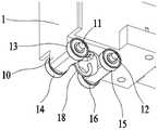
附图1为本发明激光器芯片的自动化测试装置结构示意图;1 is a schematic structural diagram of an automated testing device for a laser chip of the present invention;
附图2为本发明自动化测试装置中测试探针组件的结构示意图;2 is a schematic structural diagram of a test probe assembly in an automated test device of the present invention;
附图3为本发明自动化测试装置中测试探针组件的局部结构剖视图;3 is a partial structural cross-sectional view of the test probe assembly in the automated test device of the present invention;
附图4为本发明自动化测试装置中测试探针组件的局部结构示意图;4 is a schematic diagram of the partial structure of the test probe assembly in the automated test device of the present invention;
附图5为图4中结构的分解示意图;
附图6为本发明自动化测试装置中测试探针组件的局部结构仰视图;6 is a bottom view of the partial structure of the test probe assembly in the automated test device of the present invention;
附图7为本发明激光器芯片的自动化测试装置中探针座的结构示意图。FIG. 7 is a schematic structural diagram of a probe seat in an automated testing device for a laser chip of the present invention.
以上附图中:1、本体;2、支撑板;31、动点接触探头;32、静点接触探头;4、悬臂;5、探针座;51、探针;52、基座;53、夹片;54、调节螺母;55、V形凹槽;6、转接座;61、前挡板;62、后挡板;7、第一通孔;8、导向凹槽;9、第一销轴;10、下凸块;11、第二销轴;12、第三销轴;13、第一轴承;14、第二轴承;15、第三轴承;16、第四轴承;17、竖向通孔;18、第一弹性件;19、第四销轴;21、基板;22、测试台;23、驱动支架;231、立杆;232、安装板;233、连接板;24、测试探针组件;25、固定板;26、电机;27、丝杆;28、丝杆螺母;29、滑轨;30、滑块。In the above drawings: 1, body; 2, support plate; 31, moving point contact probe; 32, static point contact probe; 4, cantilever; 5, probe seat; 51, probe; 52, base; 53, Clip; 54, adjusting nut; 55, V-shaped groove; 6, adapter seat; 61, front baffle; 62, rear baffle; 7, first through hole; 8, guide groove; 9, first pin; 10, lower bump; 11, second pin; 12, third pin; 13, first bearing; 14, second bearing; 15, third bearing; 16, fourth bearing; 17, vertical 18, the first elastic member; 19, the fourth pin; 21, the base plate; 22, the test table; 23, the drive bracket; 231, the vertical rod; 232, the mounting plate; Probe assembly; 25, fixed plate; 26, motor; 27, lead screw; 28, lead screw nut; 29, slide rail; 30, slider.
具体实施方式Detailed ways
在本专利的描述中,需要说明的是,术语“中心”、“上”、“下”、“左”、“右”、“竖直”、“水平”、“内”、“外”等指示的方位或位置关系为基于附图所示的方位或位置关系,仅是为了便于描述本发明和简化描述,而不是指示或暗示所指的装置或元件必须具有特定的方位、以特定的方位构造和操作,因此不能理解为对本发明的限制;术语“第一”、“第二”、“第三”仅用于描述目的,而不能理解为指示或暗示相对重要性;此外,除非另有明确的规定和限定,术语“安装”、“相连”、“连接”应做广义理解,例如,可以是固定连接,也可以是可拆卸连接,或一体地连接;可以是机械连接,也可以是电连接;可以是直接相连,也可以通过中间媒介间接相连,可以是两个元件内部的连通。对于本领域的普通技术人员而言,可以具体情况理解上述术语在本专利的具体含义。In the description of this patent, it should be noted that the terms "center", "upper", "lower", "left", "right", "vertical", "horizontal", "inner", "outer", etc. The indicated orientation or positional relationship is based on the orientation or positional relationship shown in the accompanying drawings, which is only for the convenience of describing the present invention and simplifying the description, rather than indicating or implying that the indicated device or element must have a specific orientation or a specific orientation. construction and operation, and therefore should not be construed as limiting the invention; the terms "first", "second", "third" are used for descriptive purposes only and should not be construed as indicating or implying relative importance; furthermore, unless otherwise Clearly stipulated and defined, the terms "installed", "connected" and "connected" should be understood in a broad sense, for example, it may be a fixed connection, a detachable connection, or an integral connection; it may be a mechanical connection or a Electrical connection; it can be directly connected, or indirectly connected through an intermediate medium, and it can be the internal connection of two components. For those of ordinary skill in the art, the specific meanings of the above terms in this patent can be understood in specific situations.
实施例1:一种激光器芯片的自动化测试装置,包括:基板21、安装于基板21上表面的测试台22、安装于基板21外侧的驱动支架23和安装于驱动支架23上并位于测试台22上方的测试探针组件24,所述测试探针组件24包括:与驱动支架23连接的本体1、支撑板2、用于与待测试芯片接触的探针51和动点接触探头31,所述支撑板2一端安装有一悬臂4,另一端安装有所述动点接触探头31,所述本体1下端面一侧设置有一位于动点接触探头31上部并与其对应的静点接触探头32,当探针与待测试芯片接触时,动点接触探头随支撑板转动远离静点接触探头,动、静点接触探头由相互接触的初始状态变为相互分离状态,芯片测试的控制系统接收到动、静点接触探头相互分离的信号后,执行上电操作使探针与芯片电导通,继而对芯片进行各项参数的测试,所述悬臂4远离支撑板2一端固定有一安装有所述探针51的探针座5;Embodiment 1: An automated testing device for a laser chip, comprising: a
一转接座6安装于支撑板2中部的上表面,此转接座6前侧和后侧分别具有前挡板61和后挡板62,此前挡板61和后挡板62上均开有一第一通孔7和位于第一通孔7两侧的2个导向凹槽8,一第一销轴9两端分别位于前挡板61和后挡板62各自的第一通孔7内;An
位于本体1下端面另一侧的下凸块10上平行设置有第二销轴11、第三销轴12,此第二销轴11、第三销轴12位于第一销轴9上方并位于其两侧,且第二销轴11、第三销轴12各自两端均从下凸块10前后侧延伸出,第一轴承13和第二轴承14分别套接于第二销轴11两端并位于下凸块10前后两侧,第三轴承15和第四轴承16分别套接于第三销轴12两端并位于下凸块10前后两侧;A
所述第一轴承13、第三轴承15和第二轴承14、第四轴承16分别位于下凸块10与前挡板61和后挡板62之间,位于下凸块10的竖向通孔17内的第一弹性件18一端与第一销轴9位于前挡板61和后挡板62之间的中间区域连接,另一端与位于本体1内并位于第二销轴11、第三销轴12上方的第四销轴19连接,所述第一弹性件18处于拉伸状态,从而将第一轴承13、第二轴承14、第三轴承15和第四轴承16各自的动圈与第一销轴9侧表面压持接触;The
位于第一销轴9右侧的支撑板2部分、悬臂4、探针座5和探针51的质心力矩大于位于第一销轴9左侧的支撑板2剩余部分、动点接触探头31的质心力矩。The mass center moment of the
上述探针座5包括基座52和夹片53,上述探针51位于基座52和夹片53之间,此夹片53通过调节螺母54连接到基座52上;The above-mentioned
上述基座52和夹片53与探针51接触的表面至少一个开有一供探针51嵌入的V形凹槽55;上述探针51与支撑板2的夹角为30°。At least one of the surfaces of the
实施例2:一种激光器芯片的自动化测试装置,包括:基板21、安装于基板21上表面的测试台22、安装于基板21外侧的驱动支架23和安装于驱动支架23上并位于测试台22上方的测试探针组件24,所述测试探针组件24包括:与驱动支架23连接的本体1、支撑板2、用于与待测试芯片接触的探针51和动点接触探头31,所述支撑板2一端安装有一悬臂4,另一端安装有所述动点接触探头31,所述本体1下端面一侧设置有一位于动点接触探头31上部并与其对应的静点接触探头32,所述悬臂4远离支撑板2一端固定有一安装有所述探针51的探针座5;Embodiment 2: An automated testing device for a laser chip, comprising: a
一转接座6安装于支撑板2中部的上表面,此转接座6前侧和后侧分别具有前挡板61和后挡板62,此前挡板61和后挡板62上均开有一第一通孔7和位于第一通孔7两侧的2个导向凹槽8,一第一销轴9两端分别位于前挡板61和后挡板62各自的第一通孔7内;An
位于本体1下端面另一侧的下凸块10上平行设置有第二销轴11、第三销轴12,此第二销轴11、第三销轴12位于第一销轴9上方并位于其两侧,且第二销轴11、第三销轴12各自两端均从下凸块10前后侧延伸出,第一轴承13和第二轴承14分别套接于第二销轴11两端并位于下凸块10前后两侧,第三轴承15和第四轴承16分别套接于第三销轴12两端并位于下凸块10前后两侧;A
所述第一轴承13、第三轴承15和第二轴承14、第四轴承16分别位于下凸块10与前挡板61和后挡板62之间,位于下凸块10的竖向通孔17内的第一弹性件18一端与第一销轴9位于前挡板61和后挡板62之间的中间区域连接,另一端与位于本体1内并位于第二销轴11、第三销轴12上方的第四销轴19连接,所述第一弹性件18处于拉伸状态,从而将第一轴承13、第二轴承14、第三轴承15和第四轴承16各自的动圈与第一销轴9侧表面压持接触;The
位于第一销轴9右侧的支撑板2部分、悬臂4、探针座5和探针51的质心力矩大于位于第一销轴9左侧的支撑板2剩余部分、动点接触探头31的质心力矩。The mass center moment of the
上述驱动支架23进一步包括两个平行设置的立杆231、连接于两个立杆231上端之间的安装板232和连接于两个立杆231下端之间的连接板233,2个上述测试探针组件24分别安装于安装板232两端的上表面上;The above-mentioned
上述驱动支架23的立杆231与基板21之间竖直设置有一安装于基板21上的固定板25,上述固定板25下部安装有一电机26,此电机26的输出轴上安装有一沿竖直方向设置丝杆27,一套装于丝杆27上的丝杆螺母28与驱动支架23的连接板233连接;A fixing
上述丝杆27两侧并位于立杆231与固定板25之间各设置有一滑轨29,上述立杆231通过至少两个滑块30与滑轨29活动连接;上述探针51与支撑板2的夹角为60°。A
采用上述激光器芯片的自动化测试装置时,通过电机驱动所述驱动支架带动测试探针组件移动,使测试探针组件上的探针与测试台上的待测试的芯片接触,探针对芯片施加向下的压力的同时受到来自芯片的向上的反作用力,带动支撑板转动,安装于支撑板上的动点接触探头向下移动,由与静点接触探头接触的初始状态变为与静点接触探头分开的状态,表示探针已经对芯片施加了合适的压力,此时,芯片测试的控制系统执行上电操作使探针与芯片电导通、对芯片进行各项参数的测试,测试完成后,支撑板在第二弹性件的作用下反向转动,恢复至初始的水平位置,同时动点接触探头与静点接触探头接触;When the above-mentioned automatic testing device for laser chips is used, the drive bracket is driven by the motor to drive the test probe assembly to move, so that the probe on the test probe assembly is in contact with the chip to be tested on the test table, and the probe applies a direction to the chip. At the same time, it is subjected to the upward reaction force from the chip, which drives the support plate to rotate, and the moving point contact probe installed on the support plate moves downward, from the initial state of contact with the static point contact probe to the static point contact probe. The separated state means that the probe has applied appropriate pressure to the chip. At this time, the control system of the chip test performs a power-on operation to make the probe and the chip electrically connected, and test various parameters of the chip. After the test is completed, the support The plate rotates in the opposite direction under the action of the second elastic member and returns to the initial horizontal position, and at the same time the moving point contact probe contacts the static point contact probe;
在长期对大量芯片进行测试、支撑板往复转动的过程中,通过第一弹性件使得安装于支撑板上的第一销轴与其两侧、两端且安装于本体上的四个轴承贴合,在保证支撑板可以以第一销轴为支点顺畅转动的同时,实现对第一销轴的精确限位,使得支撑板只能转动而不会发生其他方向上的偏移;从而可以在实现对大量芯片进行性能测试的基础上,消除采用采用弹簧片支撑结构对前端探针结构进行支撑的现有技术中存在的疲劳性问题,有利于准确设置水平和竖直方向的位置参数,在长期、高频率的使用后,仍能保持初始压力设定值的稳定,从而提高了检测数据的稳定性、重复性、可比较性和一致性,也克服了探针与芯片脱离时,探针存在竖直方向的微小抖动的缺陷,从而有利于缩短相邻检测之间的时间,从而提高了检测效率并避免对芯片的不必要的损坏;During the long-term testing of a large number of chips and the reciprocating rotation of the support plate, the first pin shaft mounted on the support plate is made to fit with the four bearings on both sides and both ends of the support plate installed on the body through the first elastic member. While ensuring that the support plate can rotate smoothly with the first pin shaft as the fulcrum, the precise position limit of the first pin shaft is realized, so that the support plate can only be rotated without deviation in other directions; Based on the performance test of a large number of chips, the fatigue problem in the prior art that uses the spring leaf support structure to support the front-end probe structure is eliminated, which is beneficial to accurately set the position parameters in the horizontal and vertical directions. After high-frequency use, the stability of the initial pressure setting value can still be maintained, thereby improving the stability, repeatability, comparability and consistency of the detection data, and also overcomes the vertical position of the probe when the probe is separated from the chip. The defect of micro-jitter in the straight direction is beneficial to shorten the time between adjacent inspections, thereby improving the inspection efficiency and avoiding unnecessary damage to the chip;
进一步的,同时也消除了探针在水平方向的微小旋转偏移,保证了检测数据的准确性,进一步提高了检测数据的稳定性、重复性、可比较性和一致性。Further, the slight rotational offset of the probe in the horizontal direction is also eliminated, the accuracy of the detection data is ensured, and the stability, repeatability, comparability and consistency of the detection data are further improved.
本发明激光器芯片的自动化测试装置,可扩展到半导体芯片测试的其他行业,用途不仅限于光通信行业,所有需要用到激光器芯片的自动化测试装置的行业,都可以同步扩展使用,适应范围广。The automatic testing device of the laser chip of the present invention can be extended to other industries of semiconductor chip testing, and the application is not limited to the optical communication industry. All industries that need the automatic testing device of the laser chip can be simultaneously expanded and used, and the application range is wide.
上述实施例只为说明本发明的技术构思及特点,其目的在于让熟悉此项技术的人士能够了解本发明的内容并据以实施,并不能以此限制本发明的保护范围。凡根据本发明精神实质所作的等效变化或修饰,都应涵盖在本发明的保护范围之内。The above-mentioned embodiments are only intended to illustrate the technical concept and characteristics of the present invention, and the purpose thereof is to enable those who are familiar with the art to understand the content of the present invention and implement them accordingly, and cannot limit the protection scope of the present invention. All equivalent changes or modifications made according to the spirit of the present invention should be included within the protection scope of the present invention.
Claims (4)
Translated fromChinesePriority Applications (1)
| Application Number | Priority Date | Filing Date | Title |
|---|---|---|---|
| CN202210305776.9ACN114675164B (en) | 2021-07-28 | 2021-07-28 | Automatic testing device for laser chips |
Applications Claiming Priority (2)
| Application Number | Priority Date | Filing Date | Title |
|---|---|---|---|
| CN202110856380.9ACN113533938B (en) | 2021-07-28 | 2021-07-28 | Chip testing machine |
| CN202210305776.9ACN114675164B (en) | 2021-07-28 | 2021-07-28 | Automatic testing device for laser chips |
Related Parent Applications (1)
| Application Number | Title | Priority Date | Filing Date |
|---|---|---|---|
| CN202110856380.9ADivisionCN113533938B (en) | 2021-07-28 | 2021-07-28 | Chip testing machine |
Publications (2)
| Publication Number | Publication Date |
|---|---|
| CN114675164Atrue CN114675164A (en) | 2022-06-28 |
| CN114675164B CN114675164B (en) | 2025-05-13 |
Family
ID=78121139
Family Applications (3)
| Application Number | Title | Priority Date | Filing Date |
|---|---|---|---|
| CN202110856380.9AActiveCN113533938B (en) | 2021-07-28 | 2021-07-28 | Chip testing machine |
| CN202210305776.9AActiveCN114675164B (en) | 2021-07-28 | 2021-07-28 | Automatic testing device for laser chips |
| CN202210313127.3APendingCN115684867A (en) | 2021-07-28 | 2021-07-28 | Efficient test equipment for light emitting devices |
Family Applications Before (1)
| Application Number | Title | Priority Date | Filing Date |
|---|---|---|---|
| CN202110856380.9AActiveCN113533938B (en) | 2021-07-28 | 2021-07-28 | Chip testing machine |
Family Applications After (1)
| Application Number | Title | Priority Date | Filing Date |
|---|---|---|---|
| CN202210313127.3APendingCN115684867A (en) | 2021-07-28 | 2021-07-28 | Efficient test equipment for light emitting devices |
Country Status (1)
| Country | Link |
|---|---|
| CN (3) | CN113533938B (en) |
Cited By (2)
| Publication number | Priority date | Publication date | Assignee | Title |
|---|---|---|---|---|
| CN115219750A (en)* | 2022-07-07 | 2022-10-21 | 深圳市斯纳达科技有限公司 | Three-dimensional electric probe base with force feedback |
| CN116990564A (en)* | 2023-09-27 | 2023-11-03 | 武汉精毅通电子技术有限公司 | Correction device and correction method for cantilever probe |
Families Citing this family (5)
| Publication number | Priority date | Publication date | Assignee | Title |
|---|---|---|---|---|
| CN113533938B (en)* | 2021-07-28 | 2022-02-18 | 苏州联讯仪器有限公司 | Chip testing machine |
| CN116859215A (en)* | 2021-11-09 | 2023-10-10 | 苏州联讯仪器股份有限公司 | Chip test equipment for optical communication |
| CN114355132B (en)* | 2021-11-09 | 2024-03-01 | 苏州联讯仪器股份有限公司 | Laser chip test system for optical communication |
| CN114878873B (en)* | 2022-05-24 | 2024-10-15 | 苏州联讯仪器股份有限公司 | Probe adjusting bracket for chip test |
| CN119716173B (en)* | 2025-02-28 | 2025-06-17 | 南京银茂微电子制造有限公司 | A fully automatic probe testing device and method for chip |
Citations (7)
| Publication number | Priority date | Publication date | Assignee | Title |
|---|---|---|---|---|
| JPS63259263A (en)* | 1986-11-25 | 1988-10-26 | Tokyo Electron Ltd | Rotating and moving equipment for weighty object |
| GB9509089D0 (en)* | 1995-05-04 | 1995-06-28 | Guralp Sys Ltd | Seismometers and the like |
| JPH09148388A (en)* | 1995-11-16 | 1997-06-06 | Tokyo Electron Ltd | Probe unit |
| US6002426A (en)* | 1997-07-02 | 1999-12-14 | Cerprobe Corporation | Inverted alignment station and method for calibrating needles of probe card for probe testing of integrated circuits |
| RU192077U1 (en)* | 2019-05-17 | 2019-09-03 | Федеральное государственное автономное образовательное учреждение высшего образования "Дальневосточный федеральный университет" (ДВФУ) | Stir friction welding tool |
| CN113533938A (en)* | 2021-07-28 | 2021-10-22 | 苏州联讯仪器有限公司 | Chip tester |
| CN116699364A (en)* | 2023-06-08 | 2023-09-05 | 厦门新晟义集成电路有限公司 | Chip testing machine with pipeline structure |
Family Cites Families (7)
| Publication number | Priority date | Publication date | Assignee | Title |
|---|---|---|---|---|
| CN2457596Y (en)* | 2000-12-27 | 2001-10-31 | 中国科学院上海技术物理研究所 | Adjustable constant pressure probe drive frame |
| KR100768914B1 (en)* | 2006-03-17 | 2007-10-23 | 양 전자시스템 주식회사 | Probe inspection device |
| CN202757956U (en)* | 2012-08-01 | 2013-02-27 | 旺矽科技股份有限公司 | rotatable edge finder |
| CN202770869U (en)* | 2012-08-22 | 2013-03-06 | 旺矽科技股份有限公司 | Probe and edge finder using it |
| CN203535079U (en)* | 2013-09-12 | 2014-04-09 | 旺矽科技股份有限公司 | Probe apparatus |
| CN207396556U (en)* | 2017-08-01 | 2018-05-22 | 深圳市矽电半导体设备有限公司 | Probe mounting structure and LED core chip test system |
| CN109387773A (en)* | 2018-10-22 | 2019-02-26 | 青岛海信宽带多媒体技术有限公司 | Powering on mechanism |
- 2021
- 2021-07-28CNCN202110856380.9Apatent/CN113533938B/enactiveActive
- 2021-07-28CNCN202210305776.9Apatent/CN114675164B/enactiveActive
- 2021-07-28CNCN202210313127.3Apatent/CN115684867A/enactivePending
Patent Citations (7)
| Publication number | Priority date | Publication date | Assignee | Title |
|---|---|---|---|---|
| JPS63259263A (en)* | 1986-11-25 | 1988-10-26 | Tokyo Electron Ltd | Rotating and moving equipment for weighty object |
| GB9509089D0 (en)* | 1995-05-04 | 1995-06-28 | Guralp Sys Ltd | Seismometers and the like |
| JPH09148388A (en)* | 1995-11-16 | 1997-06-06 | Tokyo Electron Ltd | Probe unit |
| US6002426A (en)* | 1997-07-02 | 1999-12-14 | Cerprobe Corporation | Inverted alignment station and method for calibrating needles of probe card for probe testing of integrated circuits |
| RU192077U1 (en)* | 2019-05-17 | 2019-09-03 | Федеральное государственное автономное образовательное учреждение высшего образования "Дальневосточный федеральный университет" (ДВФУ) | Stir friction welding tool |
| CN113533938A (en)* | 2021-07-28 | 2021-10-22 | 苏州联讯仪器有限公司 | Chip tester |
| CN116699364A (en)* | 2023-06-08 | 2023-09-05 | 厦门新晟义集成电路有限公司 | Chip testing machine with pipeline structure |
Non-Patent Citations (2)
| Title |
|---|
| BEADLE, BM 等: "Modeling and parameter identification of an active anti-vibration system", 《SMART STRUCTURES AND MATERIALS 2005 CONFERENCE》, 31 December 2005 (2005-12-31), pages 23 - 34* |
| 吕磊;: "自动真空探针台技术研究", 电子工业专用设备, no. 03, 20 June 2020 (2020-06-20), pages 70 - 74* |
Cited By (4)
| Publication number | Priority date | Publication date | Assignee | Title |
|---|---|---|---|---|
| CN115219750A (en)* | 2022-07-07 | 2022-10-21 | 深圳市斯纳达科技有限公司 | Three-dimensional electric probe base with force feedback |
| CN115219750B (en)* | 2022-07-07 | 2024-06-07 | 深圳市斯纳达科技有限公司 | Three-dimensional electric probe seat with force feedback |
| CN116990564A (en)* | 2023-09-27 | 2023-11-03 | 武汉精毅通电子技术有限公司 | Correction device and correction method for cantilever probe |
| CN116990564B (en)* | 2023-09-27 | 2024-03-15 | 武汉精毅通电子技术有限公司 | Correction device and correction method for cantilever probe |
Also Published As
| Publication number | Publication date |
|---|---|
| CN115684867A (en) | 2023-02-03 |
| CN113533938B (en) | 2022-02-18 |
| CN113533938A (en) | 2021-10-22 |
| CN114675164B (en) | 2025-05-13 |
Similar Documents
| Publication | Publication Date | Title |
|---|---|---|
| CN114675164A (en) | Automated testing device for laser chips | |
| CN107966271B (en) | Display panel test fixture | |
| CN114325295A (en) | Test method for laser chip | |
| CN115704857A (en) | Test probe station for laser chip | |
| CN114720734B (en) | A probe rack and a test platform having the same | |
| CN109406835A (en) | Arrangements of electric connection | |
| CN213658910U (en) | Chip test calibration device | |
| CN111879978B (en) | Test fixture and test device | |
| JP5504546B1 (en) | Prober | |
| CN215833555U (en) | Testing mechanism of optical communication chip | |
| CN114324988B (en) | Probe seat | |
| JP4313827B2 (en) | Inspection method of semiconductor device having spherical external electrode | |
| KR101380375B1 (en) | Probe unit for inspectinon of flat display pannel | |
| CN215866793U (en) | Probe mounting rack for chip testing | |
| CN118604568A (en) | A testing system for wafer or chip particles | |
| CN115616376A (en) | A self-adjusting flying probe module for four-terminal testing | |
| WO2005006332A1 (en) | Slider testing machine | |
| CN115184162A (en) | Micro-nano-grade material elastic modulus detection equipment, detection method and detection system | |
| JP5989471B2 (en) | Piezoelectric element supply method | |
| CN112903022A (en) | Probe test system, operation method and detection method thereof | |
| CN215866831U (en) | Adjustable probe mounting rack | |
| CN221746225U (en) | Test spring plate and test device | |
| CN219811022U (en) | VCM semi-automatic electric measuring machine | |
| CN118858711B (en) | A fine-tuning bracket for semiconductor chip testing | |
| CN221667958U (en) | Cantilever probe card needle adjustment machine |
Legal Events
| Date | Code | Title | Description |
|---|---|---|---|
| PB01 | Publication | ||
| PB01 | Publication | ||
| SE01 | Entry into force of request for substantive examination | ||
| SE01 | Entry into force of request for substantive examination | ||
| CB02 | Change of applicant information | ||
| CB02 | Change of applicant information | Address after:Building 5, No. 1508, Xiangjiang Road, Suzhou High-tech Zone, Suzhou City, Jiangsu Province 215129 Applicant after:Suzhou Lianxun Instrument Co.,Ltd. Address before:215011 Building 5, no.1508 Xiangjiang Road, high tech Zone, Suzhou City, Jiangsu Province Applicant before:STELIGHT INSTRUMENT Inc. | |
| GR01 | Patent grant | ||
| GR01 | Patent grant |