CN114665280A - Three-dimensional transmitting-receiving feed network applied to flat-panel packaged array antenna - Google Patents
Three-dimensional transmitting-receiving feed network applied to flat-panel packaged array antennaDownload PDFInfo
- Publication number
- CN114665280A CN114665280ACN202210310067.XACN202210310067ACN114665280ACN 114665280 ACN114665280 ACN 114665280ACN 202210310067 ACN202210310067 ACN 202210310067ACN 114665280 ACN114665280 ACN 114665280A
- Authority
- CN
- China
- Prior art keywords
- transceiver
- network
- port
- dimensional
- flat
- Prior art date
- Legal status (The legal status is an assumption and is not a legal conclusion. Google has not performed a legal analysis and makes no representation as to the accuracy of the status listed.)
- Granted
Links
Images


Classifications
- H—ELECTRICITY
- H01—ELECTRIC ELEMENTS
- H01Q—ANTENNAS, i.e. RADIO AERIALS
- H01Q21/00—Antenna arrays or systems
- H01Q21/0006—Particular feeding systems
- H—ELECTRICITY
- H01—ELECTRIC ELEMENTS
- H01P—WAVEGUIDES; RESONATORS, LINES, OR OTHER DEVICES OF THE WAVEGUIDE TYPE
- H01P5/00—Coupling devices of the waveguide type
- H01P5/12—Coupling devices having more than two ports
- H—ELECTRICITY
- H01—ELECTRIC ELEMENTS
- H01Q—ANTENNAS, i.e. RADIO AERIALS
- H01Q1/00—Details of, or arrangements associated with, antennas
- H01Q1/50—Structural association of antennas with earthing switches, lead-in devices or lightning protectors
- H—ELECTRICITY
- H01—ELECTRIC ELEMENTS
- H01Q—ANTENNAS, i.e. RADIO AERIALS
- H01Q1/00—Details of, or arrangements associated with, antennas
- H01Q1/52—Means for reducing coupling between antennas; Means for reducing coupling between an antenna and another structure
- H01Q1/521—Means for reducing coupling between antennas; Means for reducing coupling between an antenna and another structure reducing the coupling between adjacent antennas
- H01Q1/525—Means for reducing coupling between antennas; Means for reducing coupling between an antenna and another structure reducing the coupling between adjacent antennas between emitting and receiving antennas
- Y—GENERAL TAGGING OF NEW TECHNOLOGICAL DEVELOPMENTS; GENERAL TAGGING OF CROSS-SECTIONAL TECHNOLOGIES SPANNING OVER SEVERAL SECTIONS OF THE IPC; TECHNICAL SUBJECTS COVERED BY FORMER USPC CROSS-REFERENCE ART COLLECTIONS [XRACs] AND DIGESTS
- Y02—TECHNOLOGIES OR APPLICATIONS FOR MITIGATION OR ADAPTATION AGAINST CLIMATE CHANGE
- Y02D—CLIMATE CHANGE MITIGATION TECHNOLOGIES IN INFORMATION AND COMMUNICATION TECHNOLOGIES [ICT], I.E. INFORMATION AND COMMUNICATION TECHNOLOGIES AIMING AT THE REDUCTION OF THEIR OWN ENERGY USE
- Y02D30/00—Reducing energy consumption in communication networks
- Y02D30/70—Reducing energy consumption in communication networks in wireless communication networks
Landscapes
- Variable-Direction Aerials And Aerial Arrays (AREA)
Abstract
Translated fromChinese
Description
Translated fromChinese技术领域technical field
本发明涉及平板封装阵列天线技术领域,具体是一种应用于平板封装阵列天线的三维收发馈电网络。The invention relates to the technical field of flat-panel packaged array antennas, in particular to a three-dimensional transceiving and feeding network applied to flat-panel packaged array antennas.
背景技术Background technique
砖块式结构和瓦片式结构是两种基本的阵列结构。随着智能蒙皮技术的发展,阵面易于共性,易于集成的瓦块式结构受到了业界的广泛关注。在瓦片式结构中,为了实现高密度的集成,通常会将多个天线单元和元器件进行紧密的排列。封装天线(Antenna inPackage,AiP)技术是通过封装材料与工艺将天线集成在携带芯片的封装内,基于AIP的平板封装阵列架构的每一个封装天线单元都是功能结构独立完整的有源天线,避免了电缆连接,提高了单元的集成度,具有剖面低,易于装配的优点,而且具有较好的维修性和测试性。采用平板封装阵列架构,主要的AiP有源封装天线单元可直接按照要求对天线单元数目进行增减,只需要更改多功能天线母板和底层系统板即可实现整个相控阵天线系统的快速研发。平板封装阵列的收发馈电网络连接着天线子板和底层系统板两大模块,因此收发馈电网络结构的设计显得非常重要。Brick structure and tile structure are two basic array structures. With the development of intelligent skin technology, the tile-type structure that is easy to be common and easy to integrate has received extensive attention in the industry. In a tiled structure, in order to achieve high-density integration, multiple antenna units and components are usually closely arranged. Antenna in Package (AiP) technology integrates the antenna in the package that carries the chip through packaging materials and processes. Each packaged antenna unit of the AIP-based flat-panel package array architecture is an active antenna with independent and complete functional structure. It has the advantages of low profile, easy assembly, and good maintainability and testability. Using the flat-panel packaged array structure, the main AiP active packaged antenna units can directly increase or decrease the number of antenna units as required, and only need to change the multi-function antenna motherboard and the underlying system board to realize the rapid development of the entire phased array antenna system . The transceiver feeder network of the flat-panel package array is connected to the two modules of the antenna daughter board and the underlying system board, so the design of the transceiver feeder network structure is very important.
目前平板封装阵列天线的单元数目较多,阵元位置分布情况各异,如果不能合理规划接收网络和发射网络的布局,就会造成馈线长度过于复杂,损耗大等问题。而且随着平板封装阵列天线的发展,对多层的层叠网络的要求也越来越高。收发馈电网络不仅需要包含接收链路网络和发射链路网络,而且需要在底层预留波束控制电路和电源分配电路等底层系统板的空间,因此整体结构的剖面较高。传统多层收发馈电网络是分别将接收网络层和发射网络层设计好,然后将两层结构进行叠加成型,然而介质基板层数的增加会使同轴探针和带状线之间的连接失配,导致网络的性能恶化。此外,多层微带板的微波性能受加工工艺影响大,工艺较复杂、加工难度大。传统的多层馈电网络为了保证性能,会采用内埋式电阻进行加工,从而造成加工成本过高。At present, the number of elements of the flat-panel packaged array antenna is large, and the position distribution of the array elements is different. If the layout of the receiving network and the transmitting network cannot be reasonably planned, the length of the feeder will be too complicated and the loss will be large. In addition, with the development of flat-panel packaged array antennas, the requirements for multi-layer stacked networks are also getting higher and higher. The transceiver feeder network not only needs to include the receiving link network and the transmitting link network, but also needs to reserve space for the underlying system boards such as beam control circuits and power distribution circuits at the bottom layer, so the overall structure has a high profile. The traditional multi-layer transceiver feeder network is to design the receiving network layer and the transmitting network layer separately, and then superimpose the two-layer structure. However, the increase of the number of dielectric substrate layers will make the connection between the coaxial probe and the stripline. mismatch, resulting in the deterioration of the performance of the network. In addition, the microwave performance of the multi-layer microstrip board is greatly affected by the processing technology, which is complicated and difficult to process. In order to ensure the performance of the traditional multi-layer feeding network, embedded resistors are used for processing, resulting in high processing costs.
普通的两层介质功分网络的结构简单,设计比较容易,而在多层介质结构中设计功分器要复杂很多,为了具备良好的阻抗匹配,需要用到很多端口处的匹配转换技术,比如同轴内芯穿过多层介质基板,需要计算在不同的介质中同轴外芯半径的变化情况,合理设置金属面腐蚀孔的半径。而且由于收发馈电网络涉及到的功分器数目较多,因此需要考虑各个功分网络之间的连接方式,以及每个功分网络输入端口和输出端口的结构形式等。对于多路功分网络,需要根据实际的结构分布,将同轴线转带状线连接部位,以及带状线转同轴线连接部位进行合理设计来保证性能。由于收发馈电网络会涉及到非常多的单元,因此最终整体的结构尺寸和体积较大,如果对网络匹配性能产生影响的因素没有提前加以考虑,只是依靠后期的调试优化来解决是极为困难的。The structure of the ordinary two-layer dielectric power division network is simple and the design is relatively easy, while the design of the power divider in the multi-layer dielectric structure is much more complicated. In order to have good impedance matching, many matching conversion technologies at the ports are required, such as The coaxial inner core passes through the multi-layer dielectric substrate, and it is necessary to calculate the change of the radius of the coaxial outer core in different media, and reasonably set the radius of the corrosion hole on the metal surface. Moreover, since the number of power dividers involved in the transceiver feeder network is relatively large, it is necessary to consider the connection mode between each power division network, as well as the structural form of the input port and output port of each power division network. For a multi-channel power division network, it is necessary to reasonably design the coaxial to stripline connection and the stripline to coaxial connection according to the actual structure distribution to ensure performance. Since there are many units involved in the transceiver feeder network, the final overall structure size and volume are relatively large. If the factors affecting the network matching performance are not considered in advance, it is extremely difficult to solve the problem by only relying on later debugging and optimization. .
发明内容SUMMARY OF THE INVENTION
为克服现有技术的不足,本发明提供了一种应用于平板封装阵列天线的三维收发馈电网络,解决现有技术存在的剖面高、集成度低、结构尺寸和体积较大、隔离性能不佳、加工难度大、成本较高等问题。In order to overcome the deficiencies of the prior art, the present invention provides a three-dimensional transceiving and feeding network applied to a flat-panel packaged array antenna, which solves the problems of high profile, low integration, large structural size and volume, and poor isolation performance in the prior art. It is difficult to process, and the cost is high.
本发明解决上述问题所采用的技术方案是:The technical scheme adopted by the present invention to solve the above problems is:
一种应用于平板封装阵列天线的三维收发馈电网络,包括多个拼接的三维收发一体功分器,所述三维收发一体功分器包括底板、收发馈电网络、一个发射总端口、一个接收总端口、多个输出口,所述发射总端口、所述接收总端口设于所述底板的下表面,所述收发馈电网络、所述输出口设于所述底板的上表面,所述收发馈电网络与所述发射总端口、所述接收总端口、所述输出口电相连。A three-dimensional transceiver feeder network applied to a flat-panel packaged array antenna includes a plurality of spliced three-dimensional transceiver integrated power dividers, wherein the three-dimensional transceiver integrated power divider includes a base plate, a transceiver feeder network, a main transmitting port, a receiving A main port and a plurality of output ports, the transmitting main port and the receiving main port are arranged on the lower surface of the base plate, the transceiver feeding network and the output ports are arranged on the upper surface of the base plate, the The transceiver feeding network is electrically connected to the transmitting main port, the receiving main port and the output port.
作为一种优选的技术方案,还包括多个隔离电阻,所述隔离电阻设于所述底板的下表面,所述隔离电阻与所述收发馈电网络电相连。As a preferred technical solution, it also includes a plurality of isolation resistors, the isolation resistors are arranged on the lower surface of the base plate, and the isolation resistors are electrically connected to the transceiver feeder network.
作为一种优选的技术方案,所述隔离电阻为贴片电阻,所述隔离电阻与所述底板的下表面焊接连接。As a preferred technical solution, the isolation resistor is a chip resistor, and the isolation resistor is connected to the lower surface of the base plate by welding.
作为一种优选的技术方案,所述收发馈电网络包括多层介质基板层、多层半固化片层,所述介质基板层与所述多层半固化片层层叠交错布置。As a preferred technical solution, the transceiving and feeding network includes a multi-layer dielectric substrate layer and a multi-layer prepreg layer, and the dielectric substrate layer and the multi-layer prepreg layer are stacked and alternately arranged.
作为一种优选的技术方案,所述介质基板层为4层介质基板,所述半固化片层为4层半固化片PP。As a preferred technical solution, the dielectric substrate layer is a 4-layer dielectric substrate, and the prepreg layer is a 4-layer prepreg PP.
作为一种优选的技术方案,在发射总端口、一个接收总端口、多个输出口及隔离电阻外均环绕有金属孔。As a preferred technical solution, metal holes are surrounded by the main transmitting port, the main receiving port, the multiple output ports and the isolation resistor.
作为一种优选的技术方案,所述底板上设有空气腔。As a preferred technical solution, an air cavity is provided on the bottom plate.
作为一种优选的技术方案,接收总端口、发射总端口及输出口采用同轴线或带状线与外部电相连。As a preferred technical solution, the main receiving port, the main transmitting port and the output port are electrically connected to the outside by using a coaxial line or a strip line.
作为一种优选的技术方案,还包括环绕于所述收发馈电网络外的封闭式的隔离墙。As a preferred technical solution, it also includes a closed isolation wall surrounding the outside of the transceiver feeder network.
作为一种优选的技术方案,所述收发馈电网络包括接收网络、发射网络,接收网络与发射网络接收网络与发射网络位于不同的介质基板层。As a preferred technical solution, the transceiver feeder network includes a receiving network and a transmitting network, and the receiving network and the transmitting network are located at different dielectric substrate layers.
本发明相比于现有技术,具有以下有益效果:Compared with the prior art, the present invention has the following beneficial effects:
(1)本发明解决了多功能天线母板上收发馈电网络的设计问题,采用本发明设计的三维收发一体功分器,以及组成的三维收发馈电网络同时满足低剖面、收发一体化、高隔离和低成本等优点。本发明提供了设计三维收发一体功分器和三维收发馈电网络的完整方案和思路,并根据实际的设计和加工情况,提供了良好的解决方案;(1) The present invention solves the design problem of the transceiver feeder network on the multi-function antenna motherboard, adopts the three-dimensional transceiver integrated power divider designed by the present invention, and the composed three-dimensional transceiver feeder network simultaneously satisfies the low profile, transceiver integration, advantages such as high isolation and low cost. The invention provides a complete scheme and idea for designing a three-dimensional transceiver integrated power divider and a three-dimensional transceiver feeder network, and provides a good solution according to the actual design and processing conditions;
(2)本发明设计思路清晰,通用性强;不同于传统的多层收发馈电网络,本发明的接收网络层和发射网络层不是分开设计好之后,将两层进行叠加成型,而是直接设计三维收发一体功分器,然后再拼接组成三维收发馈电网络。由于印制板层数的变化会影响网络结构的匹配特性,因此采用本发明在设计单个功分器时就直接采用多层结构进行优化设计,所提供的三维收发一体功分器在结构上给接收馈电网络和发射馈电网络都留有空间,且互不干扰;本发明所提供的三种三维收发一体功分器具备馈电网络开端,中段和结尾部分,可以根据收发馈电网络的大小和结构进行灵活的变化,因此本发明可以根据实际设计需要,灵活变化为8分路或16分路等收发馈电网络;(2) The design idea of the present invention is clear and the versatility is strong; different from the traditional multi-layer transceiver feeder network, the receiving network layer and the transmitting network layer of the present invention are not designed separately, and the two layers are superimposed and formed, but directly Design a three-dimensional transceiver integrated power divider, and then splicing to form a three-dimensional transceiver feeder network. Since the change of the number of layers of the printed board will affect the matching characteristics of the network structure, the present invention directly adopts the multi-layer structure to optimize the design when designing a single power divider. The receiving feeder network and the transmitting feeder network have space and do not interfere with each other; the three-dimensional transceiver integrated power divider provided by the present invention has the beginning, middle and end parts of the feeder network, which can be adjusted according to the size of the transceiver feeder network. and the structure can be flexibly changed, so the present invention can be flexibly changed to 8-way or 16-way and other transceiver feeder networks according to actual design needs;
(3)本发明设计结构简单,加工制造成本低;本发明尽力避免工艺较复杂、加工难度较大的方案,在保证性能的情况下,尽可能地降低成本。本发明不采用内埋式电阻,而是将隔离电阻统一放置在电路板底部,采用贴片电阻焊接,因此可以降低加工成本和复杂性。此外,本发明将结构上大部分的通孔都全部打通,减少后期背钻的使用,降低加工制造成本。同时本发明在设计三维收发一体功分器时采用了转换接头匹配技术、空气背腔和馈线隔离墙等技术,解决了多层结构收发馈电网络匹配恶化等难题;(3) The present invention has a simple design structure and low manufacturing cost; the present invention tries its best to avoid solutions with complicated processes and difficult processing, and reduces costs as much as possible while ensuring performance. The present invention does not use embedded resistors, but uniformly places the isolation resistors at the bottom of the circuit board, and adopts chip resistance welding, so that the processing cost and complexity can be reduced. In addition, in the present invention, most of the through holes on the structure are all opened, so as to reduce the use of back drilling in the later stage, and reduce the processing and manufacturing cost. At the same time, when designing the three-dimensional transceiver integrated power divider, the present invention adopts the technology of conversion joint matching, air back cavity and feeder isolation wall, etc., so as to solve the problems such as the matching deterioration of the multi-layer structure transceiver feeder network;
(4)本发明设计效率高;从整体结构出发规划网络可以尽可能地减少馈线长度,降低损耗,降低结构复杂度。此外,所提出的三维收发一体功分器在设计时就充分考虑了多层结构对馈电网络的影响,后期采用多个三维收发一体功分器拼接组成的三维收发馈电网络能够很好的保持单元的性能,组成整体后不需要进行过多的调试优化,有效避免了传统收发馈电网络后期进行长时间的计算调整。(4) The present invention has high design efficiency; planning the network based on the overall structure can reduce the length of the feeder as much as possible, reduce the loss, and reduce the complexity of the structure. In addition, the proposed three-dimensional transceiver integrated power divider fully considers the influence of the multi-layer structure on the feed network in the design. To maintain the performance of the unit, there is no need to carry out too much debugging and optimization after forming the whole, which effectively avoids the long-term calculation and adjustment of the traditional transceiver feeder network in the later stage.
附图说明Description of drawings
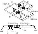
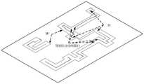
图1是平板封装相控阵天线的三维收发馈电网络;Figure 1 is a three-dimensional transceiver feed network of a flat-panel packaged phased array antenna;
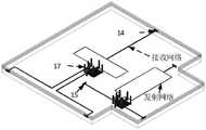
图2是平板封装相控阵天线的三维收发馈电网络的侧视图;2 is a side view of a three-dimensional transceiver feed network of a flat-panel packaged phased array antenna;
图3是多层介质基板上的三维收发一体功分器A;Figure 3 is a three-dimensional transceiver integrated power divider A on a multilayer dielectric substrate;
图4是多层介质基板上的三维收发一体功分器B;Figure 4 is a three-dimensional transceiver integrated power divider B on a multilayer dielectric substrate;
图5是多层介质基板上的三维收发一体功分器C;Figure 5 is a three-dimensional transceiver integrated power divider C on a multilayer dielectric substrate;
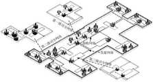
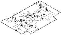
图6是多个三维收发一体功分器级联示意图;6 is a schematic diagram of a cascade of multiple three-dimensional transceiver integrated power dividers;
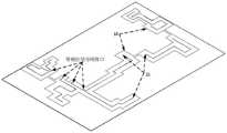
图7是根据输出口和等相位功分网络口位置设计的接收网络等相位线;Fig. 7 is the receiving network isophase line designed according to the position of the output port and the equal-phase power division network port;
图8是根据输出口和等相位功分网络口位置设计的发射网络等相位线;Fig. 8 is the equal-phase line of the transmitting network designed according to the position of the output port and the equal-phase power division network port;
图9是不带隔离墙的平板封装相控阵天线的三维收发馈电网络;Figure 9 is a three-dimensional transceiver feeder network of a flat-panel packaged phased array antenna without a partition wall;
图10是三维收发馈电网络的S参数。Figure 10 shows the S-parameters of the three-dimensional transceiver feed network.
附图中标记及相应的零部件名称:11、底板,12、收发馈电网络,13、发射总端口,14、接收总端口,15、输出口,16、隔离电阻,17、金属孔,18、隔离墙,19、空气腔,121、介质基板层,122、半固化片层。Symbols in the drawings and the corresponding parts names: 11. Bottom plate, 12, Transceiver feeder network, 13, Main transmitting port, 14, General receiving port, 15, Output port, 16, Isolation resistor, 17, Metal hole, 18 , partition wall, 19, air cavity, 121, dielectric substrate layer, 122, prepreg layer.
具体实施方式Detailed ways
下面结合实施例及附图,对本发明作进一步的详细说明,但本发明的实施方式不限于此。The present invention will be further described in detail below with reference to the embodiments and the accompanying drawings, but the embodiments of the present invention are not limited thereto.
实施例1Example 1
如图1至图10所示,本发明的目的是针对现有技术存在的不足之处,提供一种具有剖面低、集成度高、易于变化和设计、应用于平板封装阵列天线的三维收发馈电网络12,该网络由多个三维收发一体功分器组成,同时满足收发一体化、高隔离和低成本等优点。As shown in FIG. 1 to FIG. 10 , the purpose of the present invention is to provide a three-dimensional transceiver feeder with low profile, high integration, easy change and design, and applied to flat-panel packaged array antennas, aiming at the shortcomings of the prior art. The electrical network 12 is composed of a plurality of three-dimensional transceiver integrated power dividers, which simultaneously satisfy the advantages of transceiver integration, high isolation and low cost.
基于上述目的,本发明提供的技术方案如下:本发明提出的三维收发馈电网络12由多个三维收发一体功分器组成,包括一个发射总端口13,一个接收总端口14,以及16输出口15,14个隔离电阻16全部放置在网络的底部,收发馈电网络12位于介质基板层121,带状线周围采用隔离墙18进行屏蔽。本发明首先根据接收和发射天线单元的数目和分布情况,合理规划接收网络和发射网络的布局。然后从整体结构出发,设计具有多层结构的三维收发一体功分器作为每一级单元。三维收发一体功分器的介质基板层121和半固化片层122数较多,提前充分考虑多层结构对功分网络的影响,可以保证发射层和接收层互不干扰。最后将设计好的多个三维收发一体功分器拼接组成三维收发馈电网络12。Based on the above purpose, the technical solution provided by the present invention is as follows: the three-dimensional transceiver feeder network 12 proposed by the present invention is composed of a plurality of three-dimensional transceiver integrated power dividers, including a
本发明解决了多功能天线母板上收发馈电网络12的设计问题,采用本发明设计的三维收发一体功分器,以及组成的三维收发馈电网络12同时满足低剖面、收发一体化、高隔离和低成本等优点。本发明提供了设计三维收发一体功分器和三维收发馈电网络12的完整方案和思路,并根据实际的设计和加工情况,提供了良好的解决方案。The present invention solves the design problem of the transceiver feeder network 12 on the multi-function antenna motherboard, and adopts the three-dimensional transceiver integrated power divider designed by the present invention, and the three-dimensional transceiver feeder network 12 formed by the present invention simultaneously satisfies the requirements of low profile, integrated transceiver and high level. isolation and low cost. The present invention provides a complete scheme and idea for designing a three-dimensional transceiver integrated power divider and a three-dimensional transceiver feeder network 12, and provides a good solution according to the actual design and processing conditions.
本发明设计思路清晰,通用性强。不同于传统的多层收发馈电网络12,本发明的接收网络层和发射网络层不是分开设计好之后,将两层进行叠加成型,而是直接设计三维收发一体功分器,然后再拼接组成三维收发馈电网络12。由于印制板层数的变化会影响网络结构的匹配特性,因此采用本发明在设计单个功分器时就直接采用多层结构进行优化设计,所提供的三维收发一体功分器在结构上给接收馈电网络和发射馈电网络都留有空间,且互不干扰。本发明所提供的三种三维收发一体功分器具备馈电网络开端,中段和结尾部分,可以根据收发馈电网络12的大小和结构进行灵活的变化,因此本发明可以根据实际设计需要,灵活变化为8分路或16分路等收发馈电网络12。The invention has clear design ideas and strong versatility. Different from the traditional multi-layer transceiver feeder network 12, the receiving network layer and the transmitting network layer of the present invention are not designed separately, and the two layers are superimposed and formed, but a three-dimensional transceiver integrated power divider is directly designed, and then spliced to form Three-dimensional transceiver feed network 12 . Since the change of the number of layers of the printed board will affect the matching characteristics of the network structure, the present invention directly adopts the multi-layer structure to optimize the design when designing a single power divider. Space is reserved for both the receiving feeder network and the transmit feeder network, and they do not interfere with each other. The three three-dimensional transceiver integrated power dividers provided by the present invention have the beginning, middle and end parts of the feeder network, which can be flexibly changed according to the size and structure of the transceiver feeder network 12. Therefore, the present invention can flexibly change according to the actual design needs. Change to 8-way or 16-way and other transceiver feeder network 12.
本发明设计结构简单,加工制造成本低。本发明尽力避免工艺较复杂、加工难度较大的方案,在保证性能的情况下,尽可能地降低成本。本发明不采用内埋式电阻,而是将隔离电阻16统一放置在电路板底部,采用贴片电阻焊接,因此可以降低加工成本和复杂性。此外,本发明将结构上大部分的通孔都全部打通,减少后期背钻的使用,降低加工制造成本。同时本发明在设计三维收发一体功分器时采用了转换接头匹配技术、空气背腔和馈线隔离墙18等技术,解决了多层结构收发馈电网络12匹配恶化等难题。The invention has simple design structure and low processing and manufacturing cost. The present invention tries its best to avoid the scheme with complicated process and difficult processing, and reduces the cost as much as possible under the condition of guaranteeing the performance. In the present invention, instead of using embedded resistors, the
本发明设计效率高。从整体结构出发规划网络可以尽可能地减少馈线长度,降低损耗,降低结构复杂度。此外,所提出的三维收发一体功分器在设计时就充分考虑了多层结构对馈电网络的影响,后期采用多个三维收发一体功分器拼接组成的三维收发馈电网络12能够很好的保持单元的性能,组成整体后不需要进行过多的调试优化,有效避免了传统收发馈电网络12后期进行长时间的计算调整。The present invention has high design efficiency. Planning the network from the overall structure can reduce the length of the feeder as much as possible, reduce the loss, and reduce the complexity of the structure. In addition, the proposed three-dimensional transceiver integrated power divider fully considers the influence of the multi-layer structure on the feeder network in the design. The performance of the maintenance unit is maintained, and it does not need to perform too much debugging and optimization after forming a whole, which effectively avoids the long-term calculation and adjustment of the traditional transceiver feeder network 12 in the later stage.
实施例2Example 2
如图1至图10所示,作为实施例1的进一步优化,本实施例包含了实施例1的全部技术特征,除此之外,本实施例还包括以下技术特征:As shown in FIG. 1 to FIG. 10 , as a further optimization of Embodiment 1, this embodiment includes all the technical features of Embodiment 1. In addition, this embodiment also includes the following technical features:
平板封装阵列天线的三维收发馈电网络12的具体实施方式如下:The specific implementation of the three-dimensional transceiver feed network 12 of the flat-panel packaged array antenna is as follows:
(1)从整体思维设计三维收发一体功分器;(1) Design a three-dimensional transceiver integrated power divider from the overall thinking;
本发明是根据整体结构需要来设计单个性能良好的三维收发一体功分器。由于在设计单个功分器的时候就考虑介质基板层121和半固化片层122层数增加对馈电网络的影响,因此直接将单个三维收发一体功分器模型建立在具有八层基板的平板上。本发明设计的平板封装相控阵天线的三维收发馈电网络12如图1所示,馈电网络板层分布情况如图2和表1所示。包括4层介质基板,4层半固化片PP,以及1层系统板层(底板11)。设计三维收发一体功分器的时候主要考虑了以下几个方面的问题。The invention designs a single three-dimensional transceiver integrated power divider with good performance according to the needs of the overall structure. Since the influence of the increase in the number of layers of the
表1馈电网络板层分布情况Table 1 Distribution of the board layers of the feeder network


a)本发明提供的多层介质基板上的三维收发一体功分器A如图3所示,接收网络和发射网络不在同一层,两者之间有金属地板和金属墙进行屏蔽,互不干扰。在多层结构中,同轴内芯穿过其他介质之后,分界面上腐蚀圈的大小是根据介质基板的介电常数计算得到,能够使同轴内芯保持50欧姆的阻抗。a) The three-dimensional transceiver integrated power divider A on the multi-layer dielectric substrate provided by the present invention is shown in Figure 3. The receiving network and the transmitting network are not on the same layer, and there are metal floors and metal walls between the two for shielding without interfering with each other. . In the multi-layer structure, after the coaxial inner core passes through other media, the size of the corrosion circle on the interface is calculated according to the dielectric constant of the dielectric substrate, which enables the coaxial inner core to maintain an impedance of 50 ohms.
b)考虑了三维收发一体功分器隔离电阻16的放置位置,为了降低加工成本和复杂性,本发明不采用内埋式电阻,而是将隔离电阻16统一放置在电路板底部,采用贴片电阻焊接。为此我们设计了一个方便电阻安装焊接的结构,如图3所示,隔离电阻16安装位置的尺寸根据0806贴片电阻的大小进行设计。b) Considering the placement position of the
c)另外是采用金属孔17对收发功分网络进行屏蔽,如图3所示,我们在输入输出端口,以及安装隔离电阻16的周围都添加了一圈金属孔17,以此减少能量从这些区域进行传输,从而提高收发网络之间的隔离。c) In addition, metal holes 17 are used to shield the transceiver power division network. As shown in Figure 3, we have added a circle of
根据上面的方法,我们设计了第一级和第二级三维收发一体功分器网络,多层介质基板上的三维收发一体功分器A和B分别如图3和图4所示。在设计第三级三维收发一体功分器网络的时候,需要采用转接头匹配技术解决带状线转同轴线的匹配问题。多层介质基板上的三维收发一体功分器C如图5所示,为了减少引入的电感电容,我们减少了探针的长度。我们将底板11里面的探针去掉,挖空最后一层的介质基板,形成一个空气腔19,通过采用背钻技术使末端功分器具备良好的匹配。结果表明,采用这种结构可以很好地改善网络的匹配。According to the above method, we designed the first-level and second-level three-dimensional transceiver integrated power divider networks. The three-dimensional transceiver integrated power dividers A and B on the multilayer dielectric substrate are shown in Figure 3 and Figure 4, respectively. When designing the third-level three-dimensional transceiver integrated power divider network, it is necessary to use the adapter matching technology to solve the matching problem of the stripline to the coaxial line. The three-dimensional transceiver integrated power divider C on the multilayer dielectric substrate is shown in Figure 5. In order to reduce the introduced inductance and capacitance, we reduce the length of the probe. We remove the probes in the
(2)将多个三维收发一体功分器进行级联;(2) Cascading multiple three-dimensional transceiver integrated power dividers;
设计完三级功分网络之后,本发明可以根据前期规划的整体结构,很快将这些网络拼接级联成整个三维功分大网络,最终多个三维收发一体功分器级联示意图如图6所示。After the three-level power division network is designed, the present invention can quickly splicing and cascading these networks into the entire three-dimensional power division network according to the overall structure planned in the early stage. shown.
由于功分网络是多层平板结构,同轴端口和带状线端口对级联的影响很大。因此在设计功分器的时候,在不同的地方,会采用不同的端口结构来优化设计。在图3中,三维收发一体功分器A的输入端口为同轴线,输出端口选为带状线;在图4中,三维收发一体功分器B的输入端口为带状线,输出端口也选为带状线;在图5中,三维收发一体功分器C输入端口为带状线,输出端口选为同轴线。Since the power division network is a multi-layer plate structure, the coaxial port and the stripline port have a great influence on the cascade. Therefore, when designing a power divider, different port structures will be used in different places to optimize the design. In Figure 3, the input port of the three-dimensional integrated transceiver A is a coaxial line, and the output port is selected as a stripline; in Figure 4, the input port of the three-dimensional integrated transceiver B is a stripline, and the output port is a stripline. It is also selected as a strip line; in Figure 5, the input port of the three-dimensional transceiver integrated power divider C is a strip line, and the output port is selected as a coaxial line.
(3)根据输出口15设计等相位线;(3) Design iso-phase lines according to the
设计完级联的功分网络之后,就需要进一步根据整体布局设计等相位线,使接收输出端口之间或者发射输出端口之间具有相同的相位。由于馈电网络的输出端口在不同的位置,为了保证三维收发馈电网络12发射或者接收各个输出口15之间的信号是等幅同相的,因此会延长带状线的长度进行调整。如果直接将整个模型带上功分网络进行仿真,计算量太大,因此我们根据整体布局,只选取输出端口和对应的功分网络端口进行仿真,根据输出口15的和等相位功分网络口的位置设计的接收等相位线如图7所示,发射等相位线如图8所示。实践证明,通过建立简化的带状线模型进行优化设计,可以更加高效地设计出满意的结果。After designing the cascaded power division network, it is necessary to further design the equiphase lines according to the overall layout, so that the receiving output ports or the transmitting output ports have the same phase. Since the output ports of the feeding network are at different positions, in order to ensure that the signals transmitted or received by the three-dimensional transceiving and feeding network 12 between the
4)采用封闭式的隔离墙18减少干扰;4) Use a
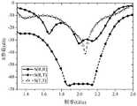
优化得到的平板封装相控阵天线的三维收发馈电网络12的如图9所示。需要注意的是,和图1的最终结构不同,该收发馈电网络12不带隔离墙18。对于尺寸较大的三维收发馈电网络12,如果不阻断一些信号在介质基板中的传播,会激励起不需要的谐振,从而产生干扰,影响收发馈电网络12的性能。为了避免这些干扰,我们在收发馈电网络12的电路边上,建立封闭式的隔离墙18,从而改善网络的隔离和匹配性能。最终设计的平板封装相控阵天线的三维收发馈电网络12如图1所示,总的收发端口的匹配以及隔离如图10所示,可以看出在需要的带宽内,收发端口的匹配良好,S11参数在-20dB以下,端口之间的隔离度高,达到65dB以上。The three-dimensional transceiver feed network 12 of the flat-panel packaged phased array antenna obtained by optimization is shown in FIG. 9 . It should be noted that, unlike the final structure in FIG. 1 , the transceiving and feeding network 12 does not have a
如上所述,可较好地实现本发明。As described above, the present invention can be preferably implemented.
以上所述,仅为本发明较佳的具体实施方式,但本发明的保护范围并不局限于此,任何熟悉本技术领域的技术人员在本发明披露的技术范围内,可轻易想到的变化或替换,都应涵盖在本发明的保护范围之内。因此,本发明的保护范围应该以权利要求书的保护范围为准。The above description is only a preferred embodiment of the present invention, but the protection scope of the present invention is not limited to this. Substitutions should be covered within the protection scope of the present invention. Therefore, the protection scope of the present invention should be based on the protection scope of the claims.
本说明书中所有实施例公开的所有特征,或隐含公开的所有方法或过程中的步骤,除了互相排斥的特征和/或步骤以外,均可以以任何方式组合和/或扩展、替换。All features disclosed in all embodiments in this specification, or steps in all methods or processes disclosed implicitly, except mutually exclusive features and/or steps, may be combined and/or expanded or replaced in any way.
以上所述,仅是本发明的较佳实施例而已,并非对本发明作任何形式上的限制,依据本发明的技术实质,在本发明的精神和原则之内,对以上实施例所作的任何简单的修改、等同替换与改进等,均仍属于本发明技术方案的保护范围之内。The above descriptions are only preferred embodiments of the present invention, and are not intended to limit the present invention in any form. According to the technical essence of the present invention, within the spirit and principles of the present invention, any simple Modifications, equivalent replacements and improvements, etc., still fall within the protection scope of the technical solution of the present invention.
Claims (10)
Translated fromChinesePriority Applications (1)
| Application Number | Priority Date | Filing Date | Title |
|---|---|---|---|
| CN202210310067.XACN114665280B (en) | 2022-03-28 | 2022-03-28 | A 3D Transceiver and Feed Network Applied to Flat Package Array Antenna |
Applications Claiming Priority (1)
| Application Number | Priority Date | Filing Date | Title |
|---|---|---|---|
| CN202210310067.XACN114665280B (en) | 2022-03-28 | 2022-03-28 | A 3D Transceiver and Feed Network Applied to Flat Package Array Antenna |
Publications (2)
| Publication Number | Publication Date |
|---|---|
| CN114665280Atrue CN114665280A (en) | 2022-06-24 |
| CN114665280B CN114665280B (en) | 2023-06-23 |
Family
ID=82034009
Family Applications (1)
| Application Number | Title | Priority Date | Filing Date |
|---|---|---|---|
| CN202210310067.XAActiveCN114665280B (en) | 2022-03-28 | 2022-03-28 | A 3D Transceiver and Feed Network Applied to Flat Package Array Antenna |
Country Status (1)
| Country | Link |
|---|---|
| CN (1) | CN114665280B (en) |
Cited By (1)
| Publication number | Priority date | Publication date | Assignee | Title |
|---|---|---|---|---|
| CN118659122A (en)* | 2024-07-30 | 2024-09-17 | 中国科学院空天信息创新研究院 | A circuit structure and design method of high isolation SAR antenna feeding assembly |
Citations (10)
| Publication number | Priority date | Publication date | Assignee | Title |
|---|---|---|---|---|
| US6300906B1 (en)* | 2000-01-05 | 2001-10-09 | Harris Corporation | Wideband phased array antenna employing increased packaging density laminate structure containing feed network, balun and power divider circuitry |
| US20150325914A1 (en)* | 2012-12-18 | 2015-11-12 | Commscope, Inc. Of North Carolina | Feed network and electromagnetic radiation source |
| CN105866747A (en)* | 2016-05-11 | 2016-08-17 | 中国电子科技集团公司第三十八研究所 | Active phased array radar transmit-receive component and manufacturing method thereof |
| CN106877004A (en)* | 2017-03-31 | 2017-06-20 | 安徽四创电子股份有限公司 | A kind of dual polarization broadband flat plate array antenna feeding network |
| CN106981720A (en)* | 2017-01-12 | 2017-07-25 | 西南电子技术研究所(中国电子科技集团公司第十研究所) | The integrated TR components of millimeter wave tile style phased array antenna |
| CN108987946A (en)* | 2018-07-30 | 2018-12-11 | 北京航空航天大学 | Slot array antenna and its power division network based on substrate integration wave-guide |
| CN208706875U (en)* | 2018-08-31 | 2019-04-05 | 北京乾中源科技有限公司 | A kind of phased array function based on strip lines configuration divides feeding network |
| CN111276787A (en)* | 2019-12-31 | 2020-06-12 | 中国电子科技集团公司第五十五研究所 | 3D Integrated Millimeter-Wave AiP Phased Array Element |
| CN112467396A (en)* | 2020-11-17 | 2021-03-09 | 上海航天电子通讯设备研究所 | Novel broadband array antenna |
| CN112886282A (en)* | 2021-03-18 | 2021-06-01 | 昆山恩电开通信设备有限公司 | Integrated network array antenna of modularization concatenation |
- 2022
- 2022-03-28CNCN202210310067.XApatent/CN114665280B/enactiveActive
Patent Citations (10)
| Publication number | Priority date | Publication date | Assignee | Title |
|---|---|---|---|---|
| US6300906B1 (en)* | 2000-01-05 | 2001-10-09 | Harris Corporation | Wideband phased array antenna employing increased packaging density laminate structure containing feed network, balun and power divider circuitry |
| US20150325914A1 (en)* | 2012-12-18 | 2015-11-12 | Commscope, Inc. Of North Carolina | Feed network and electromagnetic radiation source |
| CN105866747A (en)* | 2016-05-11 | 2016-08-17 | 中国电子科技集团公司第三十八研究所 | Active phased array radar transmit-receive component and manufacturing method thereof |
| CN106981720A (en)* | 2017-01-12 | 2017-07-25 | 西南电子技术研究所(中国电子科技集团公司第十研究所) | The integrated TR components of millimeter wave tile style phased array antenna |
| CN106877004A (en)* | 2017-03-31 | 2017-06-20 | 安徽四创电子股份有限公司 | A kind of dual polarization broadband flat plate array antenna feeding network |
| CN108987946A (en)* | 2018-07-30 | 2018-12-11 | 北京航空航天大学 | Slot array antenna and its power division network based on substrate integration wave-guide |
| CN208706875U (en)* | 2018-08-31 | 2019-04-05 | 北京乾中源科技有限公司 | A kind of phased array function based on strip lines configuration divides feeding network |
| CN111276787A (en)* | 2019-12-31 | 2020-06-12 | 中国电子科技集团公司第五十五研究所 | 3D Integrated Millimeter-Wave AiP Phased Array Element |
| CN112467396A (en)* | 2020-11-17 | 2021-03-09 | 上海航天电子通讯设备研究所 | Novel broadband array antenna |
| CN112886282A (en)* | 2021-03-18 | 2021-06-01 | 昆山恩电开通信设备有限公司 | Integrated network array antenna of modularization concatenation |
Non-Patent Citations (1)
| Title |
|---|
| 姜海玲 等: "基于微波多层印制技术的阵列馈电网络设计与实现"* |
Cited By (1)
| Publication number | Priority date | Publication date | Assignee | Title |
|---|---|---|---|---|
| CN118659122A (en)* | 2024-07-30 | 2024-09-17 | 中国科学院空天信息创新研究院 | A circuit structure and design method of high isolation SAR antenna feeding assembly |
Also Published As
| Publication number | Publication date |
|---|---|
| CN114665280B (en) | 2023-06-23 |
Similar Documents
| Publication | Publication Date | Title |
|---|---|---|
| CN201383535Y (en) | Rectangular waveguide-substrate integrated waveguide signal conversion and power divider | |
| CN100471358C (en) | A matching capacitor, printed circuit board and impedance matching device using the matching capacitor | |
| CN115224462B (en) | Microwave multilayer board interlayer interconnection matching method | |
| CN114665280B (en) | A 3D Transceiver and Feed Network Applied to Flat Package Array Antenna | |
| CN104319448B (en) | A kind of multilayer power distribution network of high frequency printed board based on attached resistive film | |
| CN206250390U (en) | A kind of suspended stripline fed planar array antenna | |
| TW202130136A (en) | Interlocking modular beamformer | |
| CN119361996B (en) | Millimeter wave terahertz microstrip-waveguide feed structure and debugging method thereof | |
| CN110012591A (en) | A kind of matrix integrated device and manufacturing method | |
| CN114024150B (en) | Active antenna array based on stripline one-to-six power division network | |
| CN113314821B (en) | Dielectric integrated suspension twisted-pair transmission line | |
| CN116742328A (en) | A compact feed tracking network | |
| CN208045696U (en) | A kind of Butler matrix feed networks based on substrate integration wave-guide | |
| CN117410664A (en) | Microstrip waveguide converter based on slot coupling technology | |
| CN108306118A (en) | A kind of extendible board-like Active Arrays | |
| CN115513676A (en) | W-band irregular circularly polarized glass-based array antenna and feed method thereof | |
| CN108304646A (en) | A kind of multidisciplined modeling and design method of multichannel chip TR components | |
| WO2021068437A1 (en) | 5g-antenna integrated network apparatus | |
| CN216928900U (en) | Split device applied to 5G large-scale array antenna calibration network | |
| CN222146553U (en) | Local oscillator power division network for vehicle-mounted radar | |
| WO2021155731A1 (en) | Active antenna array | |
| CN115494456B (en) | Radar transmitting/receiving device and radar device | |
| CN112909466B (en) | A switching board, switching network and antenna | |
| CN119812167B (en) | A multi-chip interconnection structure and preparation method thereof | |
| CN118659122B (en) | A high-isolation SAR antenna feed assembly circuit structure and design method |
Legal Events
| Date | Code | Title | Description |
|---|---|---|---|
| PB01 | Publication | ||
| PB01 | Publication | ||
| SE01 | Entry into force of request for substantive examination | ||
| SE01 | Entry into force of request for substantive examination | ||
| GR01 | Patent grant | ||
| GR01 | Patent grant |