CN114651323A - Optoelectronic device - Google Patents
Optoelectronic deviceDownload PDFInfo
- Publication number
- CN114651323A CN114651323ACN202080076222.5ACN202080076222ACN114651323ACN 114651323 ACN114651323 ACN 114651323ACN 202080076222 ACN202080076222 ACN 202080076222ACN 114651323 ACN114651323 ACN 114651323A
- Authority
- CN
- China
- Prior art keywords
- layer
- light source
- light
- optoelectronic
- optoelectronic device
- Prior art date
- Legal status (The legal status is an assumption and is not a legal conclusion. Google has not performed a legal analysis and makes no representation as to the accuracy of the status listed.)
- Pending
Links
Images


Classifications
- H—ELECTRICITY
- H01—ELECTRIC ELEMENTS
- H01L—SEMICONDUCTOR DEVICES NOT COVERED BY CLASS H10
- H01L25/00—Assemblies consisting of a plurality of semiconductor or other solid state devices
- H01L25/03—Assemblies consisting of a plurality of semiconductor or other solid state devices all the devices being of a type provided for in a single subclass of subclasses H10B, H10D, H10F, H10H, H10K or H10N, e.g. assemblies of rectifier diodes
- H01L25/04—Assemblies consisting of a plurality of semiconductor or other solid state devices all the devices being of a type provided for in a single subclass of subclasses H10B, H10D, H10F, H10H, H10K or H10N, e.g. assemblies of rectifier diodes the devices not having separate containers
- H01L25/075—Assemblies consisting of a plurality of semiconductor or other solid state devices all the devices being of a type provided for in a single subclass of subclasses H10B, H10D, H10F, H10H, H10K or H10N, e.g. assemblies of rectifier diodes the devices not having separate containers the devices being of a type provided for in group H10H20/00
- H01L25/0753—Assemblies consisting of a plurality of semiconductor or other solid state devices all the devices being of a type provided for in a single subclass of subclasses H10B, H10D, H10F, H10H, H10K or H10N, e.g. assemblies of rectifier diodes the devices not having separate containers the devices being of a type provided for in group H10H20/00 the devices being arranged next to each other
- G—PHYSICS
- G02—OPTICS
- G02B—OPTICAL ELEMENTS, SYSTEMS OR APPARATUS
- G02B27/00—Optical systems or apparatus not provided for by any of the groups G02B1/00 - G02B26/00, G02B30/00
- G02B27/10—Beam splitting or combining systems
- G02B27/12—Beam splitting or combining systems operating by refraction only
- G02B27/126—The splitting element being a prism or prismatic array, including systems based on total internal reflection
- B—PERFORMING OPERATIONS; TRANSPORTING
- B32—LAYERED PRODUCTS
- B32B—LAYERED PRODUCTS, i.e. PRODUCTS BUILT-UP OF STRATA OF FLAT OR NON-FLAT, e.g. CELLULAR OR HONEYCOMB, FORM
- B32B17/00—Layered products essentially comprising sheet glass, or glass, slag, or like fibres
- B32B17/06—Layered products essentially comprising sheet glass, or glass, slag, or like fibres comprising glass as the main or only constituent of a layer, next to another layer of a specific material
- B32B17/10—Layered products essentially comprising sheet glass, or glass, slag, or like fibres comprising glass as the main or only constituent of a layer, next to another layer of a specific material of synthetic resin
- B32B17/10005—Layered products essentially comprising sheet glass, or glass, slag, or like fibres comprising glass as the main or only constituent of a layer, next to another layer of a specific material of synthetic resin laminated safety glass or glazing
- B32B17/10009—Layered products essentially comprising sheet glass, or glass, slag, or like fibres comprising glass as the main or only constituent of a layer, next to another layer of a specific material of synthetic resin laminated safety glass or glazing characterized by the number, the constitution or treatment of glass sheets
- B32B17/10036—Layered products essentially comprising sheet glass, or glass, slag, or like fibres comprising glass as the main or only constituent of a layer, next to another layer of a specific material of synthetic resin laminated safety glass or glazing characterized by the number, the constitution or treatment of glass sheets comprising two outer glass sheets
- B—PERFORMING OPERATIONS; TRANSPORTING
- B32—LAYERED PRODUCTS
- B32B—LAYERED PRODUCTS, i.e. PRODUCTS BUILT-UP OF STRATA OF FLAT OR NON-FLAT, e.g. CELLULAR OR HONEYCOMB, FORM
- B32B17/00—Layered products essentially comprising sheet glass, or glass, slag, or like fibres
- B32B17/06—Layered products essentially comprising sheet glass, or glass, slag, or like fibres comprising glass as the main or only constituent of a layer, next to another layer of a specific material
- B32B17/10—Layered products essentially comprising sheet glass, or glass, slag, or like fibres comprising glass as the main or only constituent of a layer, next to another layer of a specific material of synthetic resin
- B32B17/10005—Layered products essentially comprising sheet glass, or glass, slag, or like fibres comprising glass as the main or only constituent of a layer, next to another layer of a specific material of synthetic resin laminated safety glass or glazing
- B32B17/10009—Layered products essentially comprising sheet glass, or glass, slag, or like fibres comprising glass as the main or only constituent of a layer, next to another layer of a specific material of synthetic resin laminated safety glass or glazing characterized by the number, the constitution or treatment of glass sheets
- B32B17/10082—Properties of the bulk of a glass sheet
- B32B17/1011—Properties of the bulk of a glass sheet having predetermined tint or excitation purity
- B—PERFORMING OPERATIONS; TRANSPORTING
- B32—LAYERED PRODUCTS
- B32B—LAYERED PRODUCTS, i.e. PRODUCTS BUILT-UP OF STRATA OF FLAT OR NON-FLAT, e.g. CELLULAR OR HONEYCOMB, FORM
- B32B17/00—Layered products essentially comprising sheet glass, or glass, slag, or like fibres
- B32B17/06—Layered products essentially comprising sheet glass, or glass, slag, or like fibres comprising glass as the main or only constituent of a layer, next to another layer of a specific material
- B32B17/10—Layered products essentially comprising sheet glass, or glass, slag, or like fibres comprising glass as the main or only constituent of a layer, next to another layer of a specific material of synthetic resin
- B32B17/10005—Layered products essentially comprising sheet glass, or glass, slag, or like fibres comprising glass as the main or only constituent of a layer, next to another layer of a specific material of synthetic resin laminated safety glass or glazing
- B32B17/10165—Functional features of the laminated safety glass or glazing
- B32B17/10174—Coatings of a metallic or dielectric material on a constituent layer of glass or polymer
- B—PERFORMING OPERATIONS; TRANSPORTING
- B32—LAYERED PRODUCTS
- B32B—LAYERED PRODUCTS, i.e. PRODUCTS BUILT-UP OF STRATA OF FLAT OR NON-FLAT, e.g. CELLULAR OR HONEYCOMB, FORM
- B32B17/00—Layered products essentially comprising sheet glass, or glass, slag, or like fibres
- B32B17/06—Layered products essentially comprising sheet glass, or glass, slag, or like fibres comprising glass as the main or only constituent of a layer, next to another layer of a specific material
- B32B17/10—Layered products essentially comprising sheet glass, or glass, slag, or like fibres comprising glass as the main or only constituent of a layer, next to another layer of a specific material of synthetic resin
- B32B17/10005—Layered products essentially comprising sheet glass, or glass, slag, or like fibres comprising glass as the main or only constituent of a layer, next to another layer of a specific material of synthetic resin laminated safety glass or glazing
- B32B17/10165—Functional features of the laminated safety glass or glazing
- B32B17/10339—Specific parts of the laminated safety glass or glazing being colored or tinted
- B32B17/10357—Specific parts of the laminated safety glass or glazing being colored or tinted comprising a tinted intermediate film
- B—PERFORMING OPERATIONS; TRANSPORTING
- B32—LAYERED PRODUCTS
- B32B—LAYERED PRODUCTS, i.e. PRODUCTS BUILT-UP OF STRATA OF FLAT OR NON-FLAT, e.g. CELLULAR OR HONEYCOMB, FORM
- B32B17/00—Layered products essentially comprising sheet glass, or glass, slag, or like fibres
- B32B17/06—Layered products essentially comprising sheet glass, or glass, slag, or like fibres comprising glass as the main or only constituent of a layer, next to another layer of a specific material
- B32B17/10—Layered products essentially comprising sheet glass, or glass, slag, or like fibres comprising glass as the main or only constituent of a layer, next to another layer of a specific material of synthetic resin
- B32B17/10005—Layered products essentially comprising sheet glass, or glass, slag, or like fibres comprising glass as the main or only constituent of a layer, next to another layer of a specific material of synthetic resin laminated safety glass or glazing
- B32B17/10165—Functional features of the laminated safety glass or glazing
- B32B17/10541—Functional features of the laminated safety glass or glazing comprising a light source or a light guide
- B—PERFORMING OPERATIONS; TRANSPORTING
- B32—LAYERED PRODUCTS
- B32B—LAYERED PRODUCTS, i.e. PRODUCTS BUILT-UP OF STRATA OF FLAT OR NON-FLAT, e.g. CELLULAR OR HONEYCOMB, FORM
- B32B27/00—Layered products comprising a layer of synthetic resin
- B32B27/30—Layered products comprising a layer of synthetic resin comprising vinyl (co)polymers; comprising acrylic (co)polymers
- B32B27/308—Layered products comprising a layer of synthetic resin comprising vinyl (co)polymers; comprising acrylic (co)polymers comprising acrylic (co)polymers
- B—PERFORMING OPERATIONS; TRANSPORTING
- B32—LAYERED PRODUCTS
- B32B—LAYERED PRODUCTS, i.e. PRODUCTS BUILT-UP OF STRATA OF FLAT OR NON-FLAT, e.g. CELLULAR OR HONEYCOMB, FORM
- B32B27/00—Layered products comprising a layer of synthetic resin
- B32B27/36—Layered products comprising a layer of synthetic resin comprising polyesters
- B32B27/365—Layered products comprising a layer of synthetic resin comprising polyesters comprising polycarbonates
- B—PERFORMING OPERATIONS; TRANSPORTING
- B60—VEHICLES IN GENERAL
- B60K—ARRANGEMENT OR MOUNTING OF PROPULSION UNITS OR OF TRANSMISSIONS IN VEHICLES; ARRANGEMENT OR MOUNTING OF PLURAL DIVERSE PRIME-MOVERS IN VEHICLES; AUXILIARY DRIVES FOR VEHICLES; INSTRUMENTATION OR DASHBOARDS FOR VEHICLES; ARRANGEMENTS IN CONNECTION WITH COOLING, AIR INTAKE, GAS EXHAUST OR FUEL SUPPLY OF PROPULSION UNITS IN VEHICLES
- B60K35/00—Instruments specially adapted for vehicles; Arrangement of instruments in or on vehicles
- B60K35/10—Input arrangements, i.e. from user to vehicle, associated with vehicle functions or specially adapted therefor
- B—PERFORMING OPERATIONS; TRANSPORTING
- B60—VEHICLES IN GENERAL
- B60K—ARRANGEMENT OR MOUNTING OF PROPULSION UNITS OR OF TRANSMISSIONS IN VEHICLES; ARRANGEMENT OR MOUNTING OF PLURAL DIVERSE PRIME-MOVERS IN VEHICLES; AUXILIARY DRIVES FOR VEHICLES; INSTRUMENTATION OR DASHBOARDS FOR VEHICLES; ARRANGEMENTS IN CONNECTION WITH COOLING, AIR INTAKE, GAS EXHAUST OR FUEL SUPPLY OF PROPULSION UNITS IN VEHICLES
- B60K35/00—Instruments specially adapted for vehicles; Arrangement of instruments in or on vehicles
- B60K35/20—Output arrangements, i.e. from vehicle to user, associated with vehicle functions or specially adapted therefor
- B—PERFORMING OPERATIONS; TRANSPORTING
- B60—VEHICLES IN GENERAL
- B60K—ARRANGEMENT OR MOUNTING OF PROPULSION UNITS OR OF TRANSMISSIONS IN VEHICLES; ARRANGEMENT OR MOUNTING OF PLURAL DIVERSE PRIME-MOVERS IN VEHICLES; AUXILIARY DRIVES FOR VEHICLES; INSTRUMENTATION OR DASHBOARDS FOR VEHICLES; ARRANGEMENTS IN CONNECTION WITH COOLING, AIR INTAKE, GAS EXHAUST OR FUEL SUPPLY OF PROPULSION UNITS IN VEHICLES
- B60K35/00—Instruments specially adapted for vehicles; Arrangement of instruments in or on vehicles
- B60K35/50—Instruments characterised by their means of attachment to or integration in the vehicle
- B—PERFORMING OPERATIONS; TRANSPORTING
- B60—VEHICLES IN GENERAL
- B60K—ARRANGEMENT OR MOUNTING OF PROPULSION UNITS OR OF TRANSMISSIONS IN VEHICLES; ARRANGEMENT OR MOUNTING OF PLURAL DIVERSE PRIME-MOVERS IN VEHICLES; AUXILIARY DRIVES FOR VEHICLES; INSTRUMENTATION OR DASHBOARDS FOR VEHICLES; ARRANGEMENTS IN CONNECTION WITH COOLING, AIR INTAKE, GAS EXHAUST OR FUEL SUPPLY OF PROPULSION UNITS IN VEHICLES
- B60K35/00—Instruments specially adapted for vehicles; Arrangement of instruments in or on vehicles
- B60K35/60—Instruments characterised by their location or relative disposition in or on vehicles
- F—MECHANICAL ENGINEERING; LIGHTING; HEATING; WEAPONS; BLASTING
- F21—LIGHTING
- F21S—NON-PORTABLE LIGHTING DEVICES; SYSTEMS THEREOF; VEHICLE LIGHTING DEVICES SPECIALLY ADAPTED FOR VEHICLE EXTERIORS
- F21S8/00—Lighting devices intended for fixed installation
- G—PHYSICS
- G02—OPTICS
- G02B—OPTICAL ELEMENTS, SYSTEMS OR APPARATUS
- G02B1/00—Optical elements characterised by the material of which they are made; Optical coatings for optical elements
- G02B1/04—Optical elements characterised by the material of which they are made; Optical coatings for optical elements made of organic materials, e.g. plastics
- G—PHYSICS
- G02—OPTICS
- G02B—OPTICAL ELEMENTS, SYSTEMS OR APPARATUS
- G02B5/00—Optical elements other than lenses
- G02B5/20—Filters
- G02B5/26—Reflecting filters
- G02B5/265—Reflecting filters involving total internal reflection
- B—PERFORMING OPERATIONS; TRANSPORTING
- B32—LAYERED PRODUCTS
- B32B—LAYERED PRODUCTS, i.e. PRODUCTS BUILT-UP OF STRATA OF FLAT OR NON-FLAT, e.g. CELLULAR OR HONEYCOMB, FORM
- B32B2457/00—Electrical equipment
- B32B2457/20—Displays, e.g. liquid crystal displays, plasma displays
- B—PERFORMING OPERATIONS; TRANSPORTING
- B32—LAYERED PRODUCTS
- B32B—LAYERED PRODUCTS, i.e. PRODUCTS BUILT-UP OF STRATA OF FLAT OR NON-FLAT, e.g. CELLULAR OR HONEYCOMB, FORM
- B32B2605/00—Vehicles
- B—PERFORMING OPERATIONS; TRANSPORTING
- B60—VEHICLES IN GENERAL
- B60K—ARRANGEMENT OR MOUNTING OF PROPULSION UNITS OR OF TRANSMISSIONS IN VEHICLES; ARRANGEMENT OR MOUNTING OF PLURAL DIVERSE PRIME-MOVERS IN VEHICLES; AUXILIARY DRIVES FOR VEHICLES; INSTRUMENTATION OR DASHBOARDS FOR VEHICLES; ARRANGEMENTS IN CONNECTION WITH COOLING, AIR INTAKE, GAS EXHAUST OR FUEL SUPPLY OF PROPULSION UNITS IN VEHICLES
- B60K2360/00—Indexing scheme associated with groups B60K35/00 or B60K37/00 relating to details of instruments or dashboards
- B60K2360/1523—Matrix displays
- B—PERFORMING OPERATIONS; TRANSPORTING
- B60—VEHICLES IN GENERAL
- B60K—ARRANGEMENT OR MOUNTING OF PROPULSION UNITS OR OF TRANSMISSIONS IN VEHICLES; ARRANGEMENT OR MOUNTING OF PLURAL DIVERSE PRIME-MOVERS IN VEHICLES; AUXILIARY DRIVES FOR VEHICLES; INSTRUMENTATION OR DASHBOARDS FOR VEHICLES; ARRANGEMENTS IN CONNECTION WITH COOLING, AIR INTAKE, GAS EXHAUST OR FUEL SUPPLY OF PROPULSION UNITS IN VEHICLES
- B60K2360/00—Indexing scheme associated with groups B60K35/00 or B60K37/00 relating to details of instruments or dashboards
- B60K2360/20—Optical features of instruments
- B60K2360/23—Optical features of instruments using reflectors
- B—PERFORMING OPERATIONS; TRANSPORTING
- B60—VEHICLES IN GENERAL
- B60K—ARRANGEMENT OR MOUNTING OF PROPULSION UNITS OR OF TRANSMISSIONS IN VEHICLES; ARRANGEMENT OR MOUNTING OF PLURAL DIVERSE PRIME-MOVERS IN VEHICLES; AUXILIARY DRIVES FOR VEHICLES; INSTRUMENTATION OR DASHBOARDS FOR VEHICLES; ARRANGEMENTS IN CONNECTION WITH COOLING, AIR INTAKE, GAS EXHAUST OR FUEL SUPPLY OF PROPULSION UNITS IN VEHICLES
- B60K2360/00—Indexing scheme associated with groups B60K35/00 or B60K37/00 relating to details of instruments or dashboards
- B60K2360/20—Optical features of instruments
- B60K2360/27—Optical features of instruments using semi-transparent optical elements
- B—PERFORMING OPERATIONS; TRANSPORTING
- B60—VEHICLES IN GENERAL
- B60K—ARRANGEMENT OR MOUNTING OF PROPULSION UNITS OR OF TRANSMISSIONS IN VEHICLES; ARRANGEMENT OR MOUNTING OF PLURAL DIVERSE PRIME-MOVERS IN VEHICLES; AUXILIARY DRIVES FOR VEHICLES; INSTRUMENTATION OR DASHBOARDS FOR VEHICLES; ARRANGEMENTS IN CONNECTION WITH COOLING, AIR INTAKE, GAS EXHAUST OR FUEL SUPPLY OF PROPULSION UNITS IN VEHICLES
- B60K2360/00—Indexing scheme associated with groups B60K35/00 or B60K37/00 relating to details of instruments or dashboards
- B60K2360/77—Instrument locations other than the dashboard
- B60K2360/785—Instrument locations other than the dashboard on or in relation to the windshield or windows
- B—PERFORMING OPERATIONS; TRANSPORTING
- B60—VEHICLES IN GENERAL
- B60K—ARRANGEMENT OR MOUNTING OF PROPULSION UNITS OR OF TRANSMISSIONS IN VEHICLES; ARRANGEMENT OR MOUNTING OF PLURAL DIVERSE PRIME-MOVERS IN VEHICLES; AUXILIARY DRIVES FOR VEHICLES; INSTRUMENTATION OR DASHBOARDS FOR VEHICLES; ARRANGEMENTS IN CONNECTION WITH COOLING, AIR INTAKE, GAS EXHAUST OR FUEL SUPPLY OF PROPULSION UNITS IN VEHICLES
- B60K35/00—Instruments specially adapted for vehicles; Arrangement of instruments in or on vehicles
- B60K35/20—Output arrangements, i.e. from vehicle to user, associated with vehicle functions or specially adapted therefor
- B60K35/21—Output arrangements, i.e. from vehicle to user, associated with vehicle functions or specially adapted therefor using visual output, e.g. blinking lights or matrix displays
- B60K35/22—Display screens
- B—PERFORMING OPERATIONS; TRANSPORTING
- B60—VEHICLES IN GENERAL
- B60Y—INDEXING SCHEME RELATING TO ASPECTS CROSS-CUTTING VEHICLE TECHNOLOGY
- B60Y2200/00—Type of vehicle
- B60Y2200/10—Road Vehicles
- B60Y2200/11—Passenger cars; Automobiles
- H—ELECTRICITY
- H10—SEMICONDUCTOR DEVICES; ELECTRIC SOLID-STATE DEVICES NOT OTHERWISE PROVIDED FOR
- H10H—INORGANIC LIGHT-EMITTING SEMICONDUCTOR DEVICES HAVING POTENTIAL BARRIERS
- H10H20/00—Individual inorganic light-emitting semiconductor devices having potential barriers, e.g. light-emitting diodes [LED]
- H10H20/80—Constructional details
- H10H20/85—Packages
- H10H20/8506—Containers
- H—ELECTRICITY
- H10—SEMICONDUCTOR DEVICES; ELECTRIC SOLID-STATE DEVICES NOT OTHERWISE PROVIDED FOR
- H10H—INORGANIC LIGHT-EMITTING SEMICONDUCTOR DEVICES HAVING POTENTIAL BARRIERS
- H10H20/00—Individual inorganic light-emitting semiconductor devices having potential barriers, e.g. light-emitting diodes [LED]
- H10H20/80—Constructional details
- H10H20/85—Packages
- H10H20/855—Optical field-shaping means, e.g. lenses
- H10H20/856—Reflecting means
Landscapes
- Engineering & Computer Science (AREA)
- Physics & Mathematics (AREA)
- Chemical & Material Sciences (AREA)
- Combustion & Propulsion (AREA)
- Transportation (AREA)
- Mechanical Engineering (AREA)
- General Physics & Mathematics (AREA)
- Optics & Photonics (AREA)
- Power Engineering (AREA)
- Microelectronics & Electronic Packaging (AREA)
- General Engineering & Computer Science (AREA)
- Condensed Matter Physics & Semiconductors (AREA)
- Computer Hardware Design (AREA)
- Planar Illumination Modules (AREA)
- Led Device Packages (AREA)
- Non-Portable Lighting Devices Or Systems Thereof (AREA)
- Illuminated Signs And Luminous Advertising (AREA)
Abstract
Translated fromChinese
Description
Translated fromChinese本发明要求日期为2019年10月29日的DE申请号为10 2019 129 220.4,日期为2019年12月6日的DE申请号为10 2019 133 447.0,日期为2020年2月21日的DK申请号为PA202070101,日期为2020年5月15日的DE申请号为10 2020 113 246.8,日期为2020年5月29日的DE申请号为10 2020 114 530.6,以及日期为2020年10月9日的DE申请号为10 2020126 558.1的优先权,其公开内容在此全部并入本发明。The present invention requires DE application number 10 2019 129 220.4 dated October 29, 2019, DE application number 10 2019 133 447.0 dated December 6, 2019, and DK application dated February 21, 2020 DE application number PA202070101 dated May 15, 2020, DE application number 10 2020 113 246.8, May 29, 2020 DE application number 10 2020 114 530.6, and October 9, 2020 The priority of DE application number 10 2020126 558.1, the disclosure of which is incorporated herein in its entirety.
技术领域technical field
本发明涉及一种光电装置、制造光电装置的方法以及交通工具。The present invention relates to an optoelectronic device, a method of manufacturing the optoelectronic device, and a vehicle.
背景技术Background technique
DE 10 2017 122 852 A1公开了一种用于机动交通工具车顶的盖件,该盖件包括层堆叠。层堆叠包括以平面方式延伸的窗格、以平面方式延伸的膜以及布置在窗格和膜之间用于将膜紧固到窗格的粘合剂层。多个微型发光二极管布置在粘合剂层中。DE 10 2017122 852 A1还公开了一种机动交通工具,该机动交通工具包括具有这种盖件的机动交通工具车顶。DE 10 2017 122 852 A1 discloses a cover for a motor vehicle roof, which cover comprises a layer stack. The layer stack includes a planarly extending pane, a planarly extending membrane, and an adhesive layer disposed between the pane and the membrane for securing the membrane to the pane. A plurality of miniature light emitting diodes are arranged in the adhesive layer. DE 10 2017 122 852 A1 also discloses a motor vehicle comprising a motor vehicle roof with such a cover.
US 2019/0248122 A1公开了一种用于制造用于机动交通工具的复合窗格的方法。该方法包括提供第一窗格和第二窗格。该方法还包括在第一窗格和第二窗格之间布置塑料膜,以及在塑料膜的表面上布置发光二极管(LED)。此外,该方法包括借助于加热源将至少在LED的区域中的塑料膜局部加热成流体状态,该加热源定位在第一窗格或第二窗格的外表面上或布置成与第一窗格或第二窗格的外表面相距一定距离。另外,该方法包括将LED引入到塑料膜中,该塑料膜被加热成流体状态,使得塑料膜的预定体积移位,并且该方法包括在将LED引入到塑料膜中之后,用插入的塑料膜层压第一窗格和第二窗格。US 2019/0248122 A1 discloses a method for manufacturing a composite pane for a motor vehicle. The method includes providing a first pane and a second pane. The method also includes disposing a plastic film between the first pane and the second pane, and disposing a light emitting diode (LED) on a surface of the plastic film. Furthermore, the method comprises locally heating the plastic film at least in the region of the LEDs into a fluid state by means of a heating source positioned on the outer surface of the first pane or of the second pane or arranged in contact with the first window The outer surface of the grid or second pane is a certain distance apart. Additionally, the method includes introducing the LEDs into a plastic film, the plastic film being heated into a fluid state such that a predetermined volume of the plastic film is displaced, and the method includes, after introducing the LEDs into the plastic film, using the inserted plastic film Laminate the first pane and the second pane.
WO 2019/186513 A1公开了一种层压汽车窗玻璃,其包括外玻璃层、内玻璃层、在外和内玻璃层之间的至少一个塑料中间层,和至少一个摄像机系统,其中摄像机系统被层压在玻璃层之间作为层压件的整体永久部件。WO 2019/186513 A1 discloses a laminated automotive glazing comprising an outer glass layer, an inner glass layer, at least one plastic interlayer between the outer and inner glass layers, and at least one camera system, wherein the camera system is laminated Pressed between glass layers as an integral permanent part of the laminate.
WO 2019/008493 A1公开了一种交通工具层压板,其包括外部玻璃层、至少内部玻璃层、位于外部玻璃层和内部玻璃层之间的至少一个塑料粘合层、嵌入塑料粘合层中的至少一个LED。导线基本上被嵌入在塑料粘合层中,形成为LED供电的电路。WO 2019/008493 A1 discloses a vehicle laminate comprising an outer glass layer, at least an inner glass layer, at least one plastic adhesive layer between the outer glass layer and the inner glass layer, a plastic adhesive layer embedded in the plastic adhesive layer at least one LED. The wires are basically embedded in the plastic adhesive layer, forming the circuit that powers the LED.
本发明的根本目的是提供一种改进的光电装置。尤其地,本发明的目的是提供一种至少部分透明和/或可提供定向光的光电装置。The underlying object of the present invention is to provide an improved optoelectronic device. In particular, it is an object of the present invention to provide an optoelectronic device that is at least partially transparent and/or that can provide directional light.
发明内容SUMMARY OF THE INVENTION
该目的通过根据权利要求1的特征的光电装置来满足。在从属权利要求中描述了本发明的优选实施例。This object is met by an optoelectronic device according to the features of
在一些实施例中,一种光电装置包括:至少部分透明的载体层,其被配置为承载至少一个光电光源和/或至少一个光电检测器,以及至少部分透明的覆盖层,并且至少一个光电光源和/或至少一个光电检测器被布置在载体层上或至少部分嵌入载体层中。In some embodiments, an optoelectronic device includes an at least partially transparent carrier layer configured to carry at least one optoelectronic light source and/or at least one photodetector, and an at least partially transparent cover layer and at least one optoelectronic light source And/or at least one photodetector is arranged on the carrier layer or at least partially embedded in the carrier layer.
因此,该至少一个光电光源和/或该至少一个光电检测器可以被布置在该载体层与该覆盖层之间,而该至少一个光电光源和/或该至少一个光电检测器被布置在该载体层上或嵌入在该载体层中。由至少一个光电光源发射的光可以穿过载体层和/或覆盖层,并且在覆盖层和/或载体层的外表面上离开光电装置。Thus, the at least one photoelectric light source and/or the at least one photodetector may be arranged between the carrier layer and the cover layer, while the at least one photoelectric light source and/or the at least one photodetector are arranged on the carrier layer or embedded in the carrier layer. The light emitted by the at least one optoelectronic light source can pass through the carrier layer and/or the cover layer and exit the optoelectronic device on the outer surface of the cover layer and/or the carrier layer.
优选地,至少一个光电光源布置在载体层上或至少部分地嵌入在载体层中,使得所产生的光的至少大部分通过覆盖层的外表面或载体层的外表面离开光电装置。因此,该至少一个光电光源可以被布置成使得发生光的定向发射并且大部分光通过载体层或覆盖层离开该装置。Preferably, the at least one optoelectronic light source is arranged on the carrier layer or at least partially embedded in the carrier layer such that at least the majority of the light generated leaves the optoelectronic device through the outer surface of the cover layer or the outer surface of the carrier layer. Thus, the at least one optoelectronic light source may be arranged such that a directional emission of light occurs and most of the light leaves the device through the carrier layer or cover layer.
光电装置可以包括至少部分透明的中间层,其布置在载体层和覆盖层之间。该至少一个光电光源和/或该至少一个光电检测器可以至少部分地嵌入在该中间层中,而该至少一个光电光源和/或该至少一个光电检测器被布置在该载体层上或至少部分地嵌入在该载体层中。The optoelectronic device may comprise an at least partially transparent intermediate layer arranged between the carrier layer and the cover layer. The at least one photoelectric light source and/or the at least one photodetector may be at least partially embedded in the intermediate layer, while the at least one photoelectric light source and/or the at least one photodetector are arranged on the carrier layer or at least partially embedded in the carrier layer.
中间层可以包括或由用于将载体层粘合到覆盖层的粘合剂组成。因此,中间层可用于将载体层和覆盖层保持在一起。The intermediate layer may comprise or consist of an adhesive for bonding the carrier layer to the cover layer. Thus, the intermediate layer can be used to hold the carrier layer and the cover layer together.
至少一个光学元件,尤其是反射或吸收光学元件,可以被布置在载体层上或可以被嵌入在载体层中。光学元件可以被配置为引导由光电光源发射的光,使得光通过载体层或覆盖层离开。因此,光的定向发射是可能的。或者,光学元件可被配置为吸收入射到光学元件上的光。At least one optical element, in particular a reflective or absorbing optical element, can be arranged on the carrier layer or can be embedded in the carrier layer. The optical element may be configured to direct light emitted by the optoelectronic light source such that the light exits through the carrier layer or cover layer. Therefore, directional emission of light is possible. Alternatively, the optical element may be configured to absorb light incident on the optical element.
该至少一个光学元件和该至少一个光电光源可以是多个光学元件和多个光电光源。光学元件和光电光源可以成对布置。因此,每个光学元件可以被分配给特定的光源。光学元件可用于引导由关联光源发射的光穿过载体层或覆盖层。或者,光学元件可以吸收由关联光源发射的光。可以通过使用成对的光学元件和光电光源来改善离开光电装置的光的方向性。The at least one optical element and the at least one optoelectronic light source may be a plurality of optical elements and a plurality of optoelectronic light sources. Optical elements and optoelectronic light sources can be arranged in pairs. Thus, each optical element can be assigned to a specific light source. Optical elements can be used to guide light emitted by the associated light source through the carrier layer or cover layer. Alternatively, the optical element may absorb light emitted by the associated light source. The directionality of light exiting the optoelectronic device can be improved by using pairs of optical elements and optoelectronic light sources.
反射光学元件,尤其是反射镜或曲面镜,可以被嵌入在载体层中,并且反射光学元件可以被配置为将来自关联光电光源的光反射到覆盖层。Reflective optical elements, especially mirrors or curved mirrors, can be embedded in the carrier layer, and the reflective optical elements can be configured to reflect light from an associated optoelectronic light source to the cover layer.
该光电光源可以被布置在该载体层上或可以被嵌入在该载体层中,尤其是在该反射光学元件的前方。The optoelectronic light source can be arranged on the carrier layer or can be embedded in the carrier layer, in particular in front of the reflective optical element.
光学元件可以由吸收器构成或包括吸收器。该吸收器可以例如具有平坦吸收板的形式。该吸收器可以被配置为吸收来自该至少一个光电光源的光。The optical element may consist of or include an absorber. The absorber may for example have the form of a flat absorber plate. The absorber may be configured to absorb light from the at least one optoelectronic light source.
优选地,吸收器可以布置在载体层上和/或光电光源可以布置在吸收器上。Preferably, the absorber can be arranged on the carrier layer and/or the optoelectronic light source can be arranged on the absorber.
至少一个吸收器和至少一个光电光源可以是多个吸收器和多个光电光源。吸收器和光电光源可以成对布置。因此,每个吸收器可被分配给特定光源,使得吸收器用于至少部分地吸收由特定光源发射的入射在吸收器上的光。The at least one absorber and the at least one optoelectronic light source may be a plurality of absorbers and a plurality of optoelectronic light sources. Absorbers and optoelectronic light sources can be arranged in pairs. Thus, each absorber may be assigned to a specific light source such that the absorber serves to at least partially absorb light emitted by the specific light source incident on the absorber.
该至少一个光电光源可以被布置在该载体层的面向该覆盖层的表面上。因此,该至少一个光电光源可以夹在该载体层与该覆盖层之间,并且它可以可选地嵌入在中间层中。The at least one optoelectronic light source can be arranged on the surface of the carrier layer facing the cover layer. Thus, the at least one optoelectronic light source can be sandwiched between the carrier layer and the cover layer, and it can optionally be embedded in an intermediate layer.
至少一个光学元件、尤其是反射或吸收光学元件,可以布置在载体层的表面上,优选布置在背离覆盖层的表面上。光学元件可以位于布置有相关光源的同一表面上,或者光学元件可以位于相对置的表面上。光学元件和关联光源可以一个在另一个之上地对准。At least one optical element, in particular a reflective or absorbing optical element, can be arranged on the surface of the carrier layer, preferably on the surface facing away from the cover layer. The optical elements may be located on the same surface on which the associated light sources are arranged, or the optical elements may be located on opposite surfaces. Optical elements and associated light sources may be aligned one above the other.
优选地,光学元件由印刷在载体层表面上的涂层或结构形成。因此,可以以紧凑且成本有效的方式形成光学元件。Preferably, the optical element is formed by a coating or structure printed on the surface of the carrier layer. Thus, the optical element can be formed in a compact and cost-effective manner.
优选地,光学元件可以包括基质材料,例如TiO2或ZrO2。基质材料可提供散射中心并有效地吸收入射在基质材料上的光。因此,通过基质材料中的多重散射的光吸收是可能的。Preferably, the optical element may comprise a matrix material such as TiO2 or ZrO2 . The host material can provide scattering centers and effectively absorb light incident on the host material. Thus, light absorption by multiple scattering in the matrix material is possible.
至少一个光电光源可以包括第一组光电光源和第二组光电光源。第一组光源可以可选地与光学元件结合布置,以便向背离覆盖层的载体层表面发射光。第二组光源可以可选地与光学元件结合布置,以便向载体层的面向覆盖层的表面发射光。第一组光源和第二组光源可以被配置为彼此独立地操作。The at least one optoelectronic light source may include a first group of optoelectronic light sources and a second group of optoelectronic light sources. The first set of light sources may optionally be arranged in combination with optical elements to emit light to the surface of the carrier layer facing away from the cover layer. The second group of light sources may optionally be arranged in combination with optical elements to emit light to the surface of the carrier layer facing the cover layer. The first set of light sources and the second set of light sources may be configured to operate independently of each other.
第一组光源和第二组光源中的至少一个的光电光源可以嵌入在载体层中。优选地,用于向光源提供电力的电导体布置在载体层的表面上,尤其是在面向覆盖层的表面上。导体可以印刷在载体层的表面上。The optoelectronic light sources of at least one of the first group of light sources and the second group of light sources may be embedded in the carrier layer. Preferably, the electrical conductors for supplying power to the light source are arranged on the surface of the carrier layer, in particular on the surface facing the cover layer. The conductors can be printed on the surface of the carrier layer.
在一些实施例中,光电装置可包括至少一个光成形元件,其优选地布置在单独的层中且与至少一个光电光源对准。光成形元件可以配置为根据由至少一个光电光源提供的光来产生准直光束。这可以改善发射光的方向性。In some embodiments, the optoelectronic device may comprise at least one light shaping element, preferably arranged in a separate layer and aligned with the at least one optoelectronic light source. The light shaping element may be configured to generate a collimated light beam from light provided by the at least one optoelectronic light source. This can improve the directionality of the emitted light.
载体层可以是柔性层。载体层可以由箔或玻璃材料制成。The carrier layer may be a flexible layer. The carrier layer can be made of foil or glass material.
覆盖层可以是柔性层。覆盖层可由玻璃或塑料材料如PMMA或PC或PVB或PVA或PET制成。PMMA是指聚甲基丙烯酸甲酯,PC是指聚碳酸酯。PVB意指聚乙烯醇缩丁醛。PVA意指聚乙酸乙烯酯。PET意指聚对苯二甲酸乙二醇酯。The cover layer may be a flexible layer. The cover layer can be made of glass or plastic material such as PMMA or PC or PVB or PVA or PET. PMMA refers to polymethyl methacrylate and PC refers to polycarbonate. PVB means polyvinyl butyral. PVA means polyvinyl acetate. PET means polyethylene terephthalate.
柔性载体层和/或柔性覆盖层的使用扩展了光电装置的可能应用范围。例如,归功于柔性,光电部件可以被布置在弯曲表面上,例如在面向内部的车顶表面上。The use of flexible carrier layers and/or flexible cover layers expands the range of possible applications for optoelectronic devices. For example, thanks to the flexibility, optoelectronic components can be arranged on curved surfaces, for example on the interior facing roof surface.
光电光源可以是LED或μLED(LED发光装置,μLED代表micro-LED)或LED芯片或μLED芯片。The optoelectronic light source may be an LED or a μLED (LED light emitting device, μLED stands for micro-LED) or an LED chip or a μLED chip.
μLED是例如边缘长度小于70μm,尤其是低至小于20μm,尤其是在1μm至10μm的范围内的小LED。另一个范围在10-30μm之间。这可产生几百μm2至几十μm2的表面积。例如,μ-LED可以具有约60μm2的表面积和约8μm的边缘长度。在一些情况下,μ-LED具有5μm或更小的边缘长度,这产生小于30μm2的表面积尺寸。这种μ-LED的典型高度例如在1.5μm至10μm的范围内。A μLED is eg a small LED with an edge length of less than 70 μm, especially down to less than 20 μm, especially in the range of 1 μm to 10 μm. Another range is between 10-30 μm. This can result in surface areas of hundreds of μm2 to tens of μm2 . For example, a μ-LED may have a surface area of about 60 μm2 and an edge length of about 8 μm. In some cases, μ-LEDs have edge lengths of 5 μm or less, which result in surface area dimensions of less than 30 μm2 . Typical heights of such μ-LEDs are, for example, in the range of 1.5 μm to 10 μm.
LED可以例如具有150-200μm量级的边缘长度或小于300μm,尤其是小于150μm的边缘长度。The LEDs can, for example, have an edge length of the order of 150-200 μm or an edge length of less than 300 μm, in particular less than 150 μm.
LED或μLED可以包括LED芯片或μLED芯片和/或包覆模制件和/或壳体。光电光源也可以是LED芯片或μLED芯片,并且不能包括包覆模制件和壳体。LED芯片或μLED芯片可以包括用于向芯片提供电力的电触点。The LED or μLED may comprise an LED chip or μLED chip and/or an overmold and/or a housing. The optoelectronic light source can also be an LED chip or a μLED chip and cannot include an overmold and a housing. The LED chip or μLED chip may include electrical contacts for providing power to the chip.
本发明还涉及一种生产光电装置,尤其是根据本发明的光电装置的方法,方法包括:提供至少部分透明的载体层,将至少一个光电光源和/或至少一个光电检测器布置在该载体层上或将该至少一个光电光源和/或该至少一个光电检测器至少部分地嵌入该载体层中,并且将该载体层附接至至少部分透明的覆盖层上。The invention also relates to a method for producing an optoelectronic device, in particular an optoelectronic device according to the invention, the method comprising: providing an at least partially transparent carrier layer on which at least one optoelectronic light source and/or at least one photodetector are arranged on or at least partially embedding the at least one photoelectric light source and/or the at least one photodetector in the carrier layer, and attaching the carrier layer to the at least partially transparent cover layer.
在一些实施例中,至少部分透明的中间层包括粘合剂或由粘合剂组成,并且中间层被布置在载体层和覆盖层之间。该至少一个光电光源和/或至少一个光电检测器可以在该载体层附接至该覆盖层之前至少部分地嵌入在该中间层中。In some embodiments, the at least partially transparent intermediate layer includes or consists of an adhesive, and the intermediate layer is disposed between the carrier layer and the cover layer. The at least one photoelectric light source and/or the at least one photodetector may be at least partially embedded in the intermediate layer before the carrier layer is attached to the cover layer.
本发明还涉及包括窗户、内部设备元件或外部设备元件的交通工具,其包括根据本发明的光学装置。The invention also relates to a vehicle comprising a window, an interior equipment element or an exterior equipment element, comprising an optical device according to the invention.
在一些实施例中,一种光电装置包括:至少部分透明的中间层,尤其是透明箔,以及In some embodiments, an optoelectronic device includes an at least partially transparent intermediate layer, particularly a transparent foil, and
多个光电光源,其被布置在该中间层上或嵌入在该中间层中,以及a plurality of optoelectronic light sources arranged on or embedded in the intermediate layer, and
光电装置进一步包括以下中的至少一个:The optoelectronic device further includes at least one of the following:
优选不透明的顶层,尤其是有色箔,其被布置在中间层的上表面上,顶层包括与光源对准的多个孔口,这样使得来自光源的光可以通过与光源对准的孔口被辐射到前方,A preferably opaque top layer, especially a coloured foil, is arranged on the upper surface of the intermediate layer, the top layer comprising a plurality of apertures aligned with the light source such that light from the light source can be radiated through the apertures aligned with the light source to the front,
过滤层,其尤其地被配置为作为中性密度过滤器操作,其被布置在顶层的上表面或中间层的上表面上,以及不透明或至少部分透明的背景层,尤其是有色箔,其被布置在中间层的底表面上。A filter layer, which is especially configured to operate as a neutral density filter, is arranged on the upper surface of the top layer or the upper surface of the intermediate layer, and an opaque or at least partially transparent background layer, especially a colored foil, which is arranged on the bottom surface of the intermediate layer.
光电装置可以以模块化方式构建,尤其是通过添加一个或多个上述层。该光电装置可以例如用在交通工具中,例如用在交通工具的内部或外部。光电装置可例如用于汽车内部或外部显示器。光电装置还可用于视频墙或另一显示系统中。Optoelectronic devices can be constructed in a modular fashion, in particular by adding one or more of the above-mentioned layers. The optoelectronic device can eg be used in a vehicle, eg inside or outside the vehicle. Optoelectronic devices can be used, for example, for automotive interior or exterior displays. The optoelectronic device can also be used in a video wall or another display system.
具有与光源对准的孔口的不透明顶层可覆盖下层结构并提供改进的整体设计印象。孔口可以通过使用冲压工艺来制造。An opaque top layer with apertures aligned with the light source can cover the underlying structure and provide an improved overall design impression. The orifice can be made by using a stamping process.
可以被配置为中性密度过滤器的过滤层可以帮助平滑光源的发射特性并改善发射光的均匀性。The filter layer, which can be configured as a neutral density filter, can help smooth the emission characteristics of the light source and improve the uniformity of the emitted light.
在一些实施例中,如果背景层布置在中间层的底表面上,光电装置包括布置在中间层的底表面上或背景层的底表面上的不透明或至少部分透明的载体层。载体层可以是透明的或部分透明的,例如,如果装置用于交通工具的窗户中。例如,如果装置布置在交通工具的非透明表面上,则其可以是非透明载体层。In some embodiments, if the background layer is disposed on the bottom surface of the intermediate layer, the optoelectronic device includes an opaque or at least partially transparent carrier layer disposed on the bottom surface of the intermediate layer or on the bottom surface of the background layer. The carrier layer may be transparent or partially transparent, eg if the device is used in a vehicle window. For example, if the device is arranged on a non-transparent surface of a vehicle, it may be a non-transparent carrier layer.
在一些实施例中,光电装置的层被配置为布置在自由变形表面上,例如交通工具的自由变形表面。自由变形表面例如可以是弯曲表面。In some embodiments, the layers of the optoelectronic device are configured to be disposed on a freely deformable surface, such as a freely deformable surface of a vehicle. The freely deformable surface can be, for example, a curved surface.
在一些实施例中,光电装置的层是可弯曲的和/或柔性的。因此,这些层可以容易地布置在例如交通工具的弯曲表面上。In some embodiments, the layers of the optoelectronic device are bendable and/or flexible. Thus, these layers can be easily arranged, for example, on curved surfaces of vehicles.
顶层可以设计成一种或多种颜色。例如,可以根据交通工具的内部设计将顶层的颜色调整为环境的颜色。The top layer can be designed in one or more colors. For example, the color of the top layer can be adjusted to the color of the environment according to the interior design of the vehicle.
顶层可以由皮革、塑料材料、织物或纺织品制成。顶层可具有小于100μm或小于50μm的厚度。如果顶层由织物或纺织品制成,则顶层优选地具有在100μm至1000μm之间的范围内的层厚度。The top layer can be made of leather, plastic material, fabric or textile. The top layer may have a thickness of less than 100 μm or less than 50 μm. If the top layer is made of fabric or textile, the top layer preferably has a layer thickness in the range between 100 μm and 1000 μm.
过滤层和/或背景层可以是有色的。可以覆盖底层结构,并且可以获得改进的整体设计印象。The filter layer and/or the background layer can be colored. The underlying structure can be covered and an improved overall design impression can be obtained.
背景层可以包括与光源对准的多个孔口。来自光源的光可以通过与光源对准的孔口辐射到背部。这尤其有利于与至少部分透明的载体层结合。The background layer may include a plurality of apertures aligned with the light source. Light from the light source can be radiated to the back through an aperture aligned with the light source. This is particularly advantageous in combination with an at least partially transparent carrier layer.
在一些实施例中,一种光电装置包括:至少部分透明的中间层,尤其是透明箔,In some embodiments, an optoelectronic device includes an at least partially transparent intermediate layer, especially a transparent foil,
多个光电光源,其被布置在该中间层上或嵌入在该中间层中,以及a plurality of optoelectronic light sources arranged on or embedded in the intermediate layer, and
多个光学元件,其中每个光学元件与多个光源中的光源中的一个对准,其中光学元件与中间层一体地形成。A plurality of optical elements, wherein each optical element is aligned with one of the light sources of the plurality of light sources, wherein the optical elements are integrally formed with the intermediate layer.
在一些实施例中,至少一个并且优选地每个光学元件是以下中的一个:透镜、微透镜、用于光束成形的光学微结构。In some embodiments, at least one and preferably each optical element is one of the following: a lens, a microlens, an optical microstructure for beam shaping.
在一些实施例中,一种生产光电装置的方法包括:In some embodiments, a method of producing an optoelectronic device includes:
提供至少部分透明的中间层,尤其是透明箔,provide at least partially transparent interlayers, especially transparent foils,
在该中间层上或在该中间层中提供多个光电光源,并且providing a plurality of optoelectronic light sources on or in the intermediate layer, and
尤其地通过使用深拉工艺在该中间层中产生多个光学元件。Optical elements are produced in this intermediate layer, in particular by using a deep drawing process.
提供多个光电光源的步骤可以在产生光学元件之前或之后执行。在光电装置中,每个光学元件与多个光源中的光源中的一个对准。The step of providing the plurality of optoelectronic light sources may be performed before or after the optical elements are produced. In an optoelectronic device, each optical element is aligned with one of a plurality of light sources.
光学元件的形成可以被认为是中间层上的3D变形过程,其使得用于光束成形的微结构的产生,可以有助于在中间层变形之后保持或产生期望的发射特性。The formation of optical elements can be thought of as a 3D deformation process on the interlayer, which enables the creation of microstructures for beam shaping that can help to maintain or produce desired emission characteristics after deformation of the interlayer.
在一些实施例中,一种光电装置包括:至少部分透明的中间层,尤其是透明箔,以及In some embodiments, an optoelectronic device includes an at least partially transparent intermediate layer, particularly a transparent foil, and
多个光电光源,其布置在中间层上或嵌入中间层中,每个光源具有垂直于相应光源的顶表面的表面法线。光电装置可旨在用作具有弯曲形状的支撑表面,使得中间层呈现支撑表面的弯曲形状。光源可以布置在中间层上或嵌入中间层中,使得当中间层处于弯曲形状时,它们的表面法线彼此平行。附加地或可选地,光源可以布置在中间层上或嵌入中间层中,使得当中间层具有弯曲形状时,它们的表面法线彼此平行。A plurality of optoelectronic light sources, disposed on or embedded in the interlayer, each light source having a surface normal perpendicular to the top surface of the respective light source. The optoelectronic device may be intended to serve as a support surface having a curved shape, such that the intermediate layer assumes the curved shape of the support surface. The light sources may be arranged on or embedded in the interlayer such that their surface normals are parallel to each other when the interlayer is in a curved shape. Additionally or alternatively, the light sources may be arranged on or embedded in the interlayer such that when the interlayer has a curved shape, their surface normals are parallel to each other.
由此可以实现3D支撑表面(例如交通工具内部或外部的表面)上的恒定亮度。优选地,光源至少近似为Lambert发射器。A constant brightness on a 3D support surface, eg a surface inside or outside a vehicle, can thereby be achieved. Preferably, the light source is at least approximately a Lambert emitter.
在一些实施例中,光电装置包括至少一层电线。优选地,电线可以具有阵列状结构。优选地,阵列状结构可以包括彼此机械和/或电分离的阵列状部段。阵列状结构可以以即用状态提供,使得在光电装置的制造期间,它们可以直接结合到光电装置的层中。In some embodiments, the optoelectronic device includes at least one layer of wires. Preferably, the wires may have an array-like structure. Preferably, the array-like structure may comprise array-like segments that are mechanically and/or electrically separated from each other. The array-like structures can be provided in a ready-to-use state such that they can be incorporated directly into the layers of the optoelectronic device during fabrication of the optoelectronic device.
在一些实施例中,每条电线的至少一部分并且优选地所有电线具有小于20μm、15μm或10μm的迹线宽度,并且相邻电线具有小于150μm、125μm或100μm的间距。从而可以提高光电装置的整体透明度。尤其地,在人眼的阅读距离处,电线可以保持视觉上不可察觉。In some embodiments, at least a portion and preferably all of each wire has a trace width of less than 20 μm, 15 μm or 10 μm, and adjacent wires have a spacing of less than 150 μm, 125 μm or 100 μm. Thereby, the overall transparency of the optoelectronic device can be improved. In particular, at the reading distance of the human eye, the wires may remain visually imperceptible.
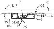
在一些实施例中,光电装置包括:多个光电光源,这些光电光源被布置在非透明载体层的表面上,以及In some embodiments, the optoelectronic device includes a plurality of optoelectronic light sources disposed on the surface of the non-transparent carrier layer, and
反射和导电材料层,尤其是金属层,其布置在光电光源和载体层之间的载体层的表面上,以及a layer of reflective and conductive material, in particular a metal layer, arranged on the surface of the carrier layer between the optoelectronic light source and the carrier layer, and
其中每个光电光源具有位于光源的底侧处的一个电触点,其中底侧面向反射和导电材料层,并且其中每个光电光源的底部处的一个电触点接触反射和导电材料层。wherein each optoelectronic light source has one electrical contact at the bottom side of the light source, wherein the bottom side faces the layer of reflective and conductive material, and wherein one electrical contact at the bottom of each optoelectronic light source contacts the layer of reflective and conductive material.
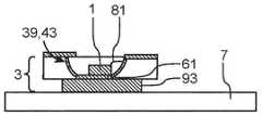
该材料层可用作反射器,并因此改善了在前向方向上的辐射特性,该前向方向是背离材料层的顶表面并相应地背离光源的顶侧的方向。The material layer can act as a reflector and thus improve the radiation properties in the forward direction, which is the direction away from the top surface of the material layer and correspondingly away from the top side of the light source.
在一些实施例中,每个光电光源具有位于光源顶侧的另一电触点。顶侧可以背离反射和导电材料层,并且每个光电光源的顶部处的电触点可以与布置在载体层的表面上并且与反射和导电材料层分离的接触焊盘连接。优选地,在每个光电光源的顶部的每个电触点和不与另一个光电光源连接的单独的接触焊盘连接。In some embodiments, each optoelectronic light source has another electrical contact on the top side of the light source. The top side may face away from the layer of reflective and conductive material, and electrical contacts at the top of each optoelectronic light source may be connected to contact pads arranged on the surface of the carrier layer and separate from the layer of reflective and conductive material. Preferably, each electrical contact on top of each optoelectronic light source is connected to a separate contact pad that is not connected to another optoelectronic light source.
载体层的表面可以包括多个空腔。在每个空腔中,可以布置多个光电光源中的一个或多个光源。在一些实施例中,反射和导电材料层尤其完全覆盖空腔的底表面,和/或空腔的侧壁,和/或相邻空腔之间的桥接部分的顶表面。镜像空腔可以帮助改善前向方向上的辐射特性。The surface of the carrier layer may comprise a plurality of cavities. In each cavity, one or more light sources of a plurality of optoelectronic light sources may be arranged. In some embodiments, the layer of reflective and conductive material especially completely covers the bottom surface of the cavity, and/or the sidewalls of the cavity, and/or the top surface of the bridge portion between adjacent cavities. A mirrored cavity can help improve the radiation characteristics in the forward direction.
在一些实施例中,光电装置包括:布置在至少部分透明的载体层的表面上的多个光电光源,以及多个反射和导电材料层元件,尤其是金属层元件,其中每个材料层元件布置在载体层的表面上并且在光电光源之一与载体层之间,In some embodiments, the optoelectronic device comprises: a plurality of optoelectronic light sources arranged on the surface of the at least partially transparent carrier layer, and a plurality of reflective and conductive material layer elements, in particular metal layer elements, wherein each material layer element is arranged on the surface of the carrier layer and between one of the optoelectronic light sources and the carrier layer,
其中该材料层元件的顶表面的面积大于该关联光源的底表面的面积,并且wherein the area of the top surface of the material layer element is greater than the area of the bottom surface of the associated light source, and
其中每个光电光源具有位于光源的底侧处的一个电触点,其中底侧面向材料层元件的顶表面,材料层元件布置在相应光源下方,并且其中每个光电光源的底部处的一个电触点接触材料层元件。wherein each optoelectronic light source has one electrical contact at the bottom side of the light source, wherein the bottom side faces the top surface of the material layer element arranged under the respective light source, and wherein one electrical contact at the bottom of each optoelectronic light source The contact contacts the material layer element.
材料层元件的顶表面的面积可以略大于关联光源的底表面的面积。例如,它可以比关联光源的底表面的面积大5-10%、10-20%或20%-30%。每个光学元件可以位于关联材料层元件的中心。The area of the top surface of the material layer element may be slightly larger than the area of the bottom surface of the associated light source. For example, it may be 5-10%, 10-20% or 20-30% larger than the area of the bottom surface of the associated light source. Each optical element may be centered on the associated material layer element.
在一些实施例中,每个光电光源具有位于光源的顶侧处的另一电触点,其中顶侧背离反射和导电材料层元件,并且其中每个光电光源的顶部处的电触点与布置在载体层的表面上并与反射和导电材料层元件分离的接触焊盘连接。In some embodiments, each optoelectronic light source has another electrical contact at the top side of the light source, wherein the top side faces away from the reflective and conductive material layer element, and wherein the electrical contact at the top of each optoelectronic light source is arranged with the Contact pads on the surface of the carrier layer and separate from the elements of the layer of reflective and conductive material are connected.
位于光电光源顶部的电触点可以和不与另一光电光源连接的单独的接触焊盘连接。各个光电光源的操作可以经由关联的接触焊盘来控制。因此,光源的单独操作是可能的。The electrical contacts on top of the photovoltaic light source can be connected to separate contact pads that are not connected to another photovoltaic light source. The operation of each optoelectronic light source can be controlled via the associated contact pads. Thus, individual operation of the light sources is possible.
在一些实施例中,非透明层,尤其是黑色或深色层布置在多个光电光源上方。非透明层包括与光源的顶表面对准的孔口,使得从光源的顶表面发射的光可以通过与光源的顶表面对准的孔口辐射。使用具有孔口的非透明层可以改善关于前向辐射的发射特性并抑制横向辐射。In some embodiments, a non-transparent layer, especially a black or dark layer, is arranged over the plurality of electro-optical light sources. The non-transparent layer includes apertures aligned with the top surface of the light source such that light emitted from the top surface of the light source can radiate through the aperture aligned with the top surface of the light source. The use of a non-transparent layer with apertures can improve the emission characteristics with respect to forward radiation and suppress lateral radiation.
在一些实施例中,挡光器可以围绕多个光源中的一个或多个光源沿周向方向布置。挡光器例如可以是布置在其中嵌入光源的透明层中的金属化小挖槽(dig)。挡光器优选地围绕形成像素的多个光源(例如三个光源)布置。像素的每个光源发射不同波长的光。例如,一个光源发射红光,一个光源发射绿光,一个光源发射蓝光。由此,可以实现RGB像素。In some embodiments, the shutters may be arranged in a circumferential direction around one or more of the plurality of light sources. The light barrier may for example be a small metallized dig arranged in the transparent layer in which the light source is embedded. The shutters are preferably arranged around a plurality of light sources (eg three light sources) forming the pixel. Each light source of a pixel emits light of a different wavelength. For example, one light source emits red light, one light source emits green light, and one light source emits blue light. Thereby, RGB pixels can be realized.
挡光器可以为电线提供通道以向被挡光器围绕的光源提供电力。The shutter may provide a passage for electrical wires to provide power to the light source surrounded by the shutter.
在一些实施例中,光电光源可以是LED或μLED。In some embodiments, the optoelectronic light sources may be LEDs or μLEDs.
本发明的另一个目的是提供至少部分透明的光电装置,其中不发生或只在很小程度上发生由背反射引起的干涉效应。Another object of the present invention is to provide at least partially transparent optoelectronic devices in which interference effects caused by back reflections do not occur or only occur to a small extent.
在一些实施例中,根据本发明的光电装置包括:至少一个光电光源,In some embodiments, an optoelectronic device according to the present invention comprises: at least one optoelectronic light source,
至少一个部分透明的前层,at least one partially transparent front layer,
至少一个部分透明的后层,at least one partially transparent back layer,
其中光源布置在前层和后层之间,The light source is arranged between the front layer and the back layer,
其中该光源的前侧面向该前层并且该光源的后侧面向该后层,并且其中提供了限制装置,其中该限制装置将光源在其中发射光的空间区域限制到限定的空间区域。Wherein the front side of the light source faces the front layer and the rear side of the light source faces the rear layer, and wherein confinement means are provided, wherein the confinement means confines the spatial area in which the light source emits light to a defined spatial area.
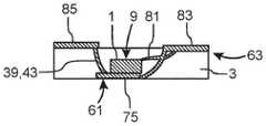
前层和后层可以是例如相应的玻璃层或至少另一种部分透明的材料。在每种情况下,前层和后层也可以是多层的。至少一个光电光源布置在前层和后层之间的层(在本文中也称为中间层)中,其中中间层也至少部分地由透明或部分透明的材料形成。The front and rear layers may be, for example, corresponding glass layers or at least another partially transparent material. In each case, the front and rear layers can also be multi-layered. At least one optoelectronic light source is arranged in a layer between the front layer and the rear layer (also referred to herein as an intermediate layer), wherein the intermediate layer is also formed at least partially from a transparent or partially transparent material.
术语“层”在本文中可在一般意义上理解且不涉及半导体材料的层结构。前和后层可以是例如单层或多层玻璃窗格。层也不必由一种材料均匀地形成。例如,其中布置有至少一个光源的中间层可以包含其它组分、填充材料和/或粘合剂材料等。The term "layer" is herein to be understood in a general sense and does not refer to layer structures of semiconductor materials. The front and rear layers may be, for example, single or multiple panes of glass. The layers also do not have to be formed uniformly from one material. For example, the intermediate layer in which the at least one light source is arranged may contain other components, filler materials and/or binder materials, and the like.
尽管这里通常只提到一个光源,但是也可以在中间层中布置多个光源。阵列状排列是尤其合适的。因此,光源可以形成显示器。每个光源可以发射来自多个预定颜色的特定颜色的光,例如红色、绿色和蓝色,以便实现RGB显示器。不同颜色的光源可以形成像素,其中相应颜色的光源形成子像素。Although only one light source is usually mentioned here, it is also possible to arrange multiple light sources in the intermediate layer. Array-like arrangements are particularly suitable. Thus, the light source can form a display. Each light source may emit light of a particular color from a plurality of predetermined colors, such as red, green, and blue, in order to implement an RGB display. Light sources of different colors may form pixels, with light sources of corresponding colors forming sub-pixels.
相对于在前层的前侧上的装置的俯视图,光源和任何其它部件(例如与相应光源关联的限制装置)由于其体积小而仅占据前侧的总横截面积的一小部分。因此,该装置保持至少部分透明,尽管部件是不透明的。Relative to the top view of the device on the front side of the front layer, the light sources and any other components (eg confinement means associated with the respective light sources) occupy only a small fraction of the total cross-sectional area of the front side due to their small size. Thus, the device remains at least partially transparent despite the opaque components.
光电光源优选为LED或μLED。The optoelectronic light source is preferably an LED or a μLED.
光电光源可以具有宽的光发射锥。例如,光源可以是Lambert辐射器,使得亮度在所有侧面上近似相同。这里的例外可以是光源的后侧,在该处没有发生光发射。The optoelectronic light source may have a broad light emission cone. For example, the light source may be a Lambert radiator such that the brightness is approximately the same on all sides. An exception here can be the rear side of the light source, where no light emission occurs.
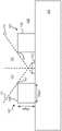
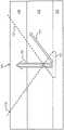
在根据本发明的光电装置中,光源被分配有限制装置,该限制装置将光源发射光的空间区域限制或变窄为限定的空间区域。尤其地,限定的空间区域可以以这样的方式被限制,即实现改进的向前辐射,即在前层的前侧方向上的辐射。In the optoelectronic device according to the invention, the light source is assigned a limiting device, which confines or narrows the spatial region from which the light source emits light to a defined spatial region. In particular, the defined spatial region can be limited in such a way that improved forward radiation is achieved, ie radiation in the direction of the front side of the front layer.
尤其有利的是,如果限制装置被设计成防止光束的传播,否则光束将以等于或大于全反射临界角的角度撞击前层的前侧和环境(通常是空气)之间的界面。因此可以减少或避免在前侧和周围环境之间的界面处光的全反射效应。由于全反射而在装置中循环的光可以在另外的界面处被反射或散射。因此,干涉光束可以出现在装置的前侧或后侧的任何地方。使用限制装置可以减少或避免基于全反射的这种破坏性影响。It is especially advantageous if the confinement means are designed to prevent the propagation of the beam which would otherwise strike the interface between the front side of the front layer and the environment (usually air) at an angle equal to or greater than the critical angle of total reflection. The effect of total reflection of light at the interface between the front side and the surrounding environment can thus be reduced or avoided. Light circulating in the device due to total reflection may be reflected or scattered at additional interfaces. Therefore, the interfering beam can appear anywhere on the front or rear side of the device. This destructive effect based on total reflection can be reduced or avoided by using confinement devices.
限制装置尤其地布置在光源的外部。因此,限制装置对光源内的光产生没有影响,而是用于在光源最初将光发射到更宽的空间区域中之后使光发射的空间区域变窄。限制装置优选地布置在前层和后层之间。限制装置尤其地位于其中布置光源的同一层中。因此,即使在由光源发射的光已经穿过例如中间层和前层之间的界面之前,光的发射的空间区域也可以限于有限的空间区域。从而可以避免或减少界面处的背反射或散射。The limiting device is arranged in particular outside the light source. Thus, the confinement means have no effect on light production within the light source, but rather serve to narrow the spatial area of light emission after the light source initially emits light into a wider spatial area. The confinement means are preferably arranged between the front layer and the rear layer. The limiting means are in particular located in the same layer in which the light sources are arranged. Thus, even before the light emitted by the light source has passed through eg the interface between the intermediate layer and the front layer, the spatial area of emission of light can be limited to a limited spatial area. Thereby back reflection or scattering at the interface can be avoided or reduced.
光发射的空间区域可以至少近似地对应于具有相对于前侧法线的开度角的发射锥,并且限制装置可以被设计成减小发射锥的开度角。由此可以实现主发射方向平行于光源前侧法线的定向发射。The spatial area of light emission may correspond at least approximately to an emission cone with an opening angle relative to the front normal, and the limiting means may be designed to reduce the opening angle of the emission cone. In this way, directional emission with the main emission direction parallel to the normal to the front side of the light source can be achieved.
有利地,如果限制装置将发射锥的开度角限制为等于或小于前层和前层前面的周围环境之间的界面处的全反射临界角的角度,则可以避免前层和周围环境之间的界面处的全反射。周围环境的光学介质通常是空气。相对于界面的法线计算开度角和临界角。Advantageously, if the limiting device limits the opening angle of the emission cone to an angle equal to or less than the critical angle of total reflection at the interface between the front layer and the surrounding environment in front of the front layer, the gap between the front layer and the surrounding environment can be avoided. total reflection at the interface. The optical medium of the surrounding environment is usually air. The opening and critical angles are calculated relative to the normal of the interface.
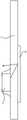
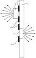
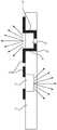
该限制装置可以具有反射器或吸收器装置,该反射器或吸收器装置在周向方向上围绕该光源和/或围绕该前侧法线的该发射区域完全周向地延伸。通过反射器或吸收器装置,可以防止由光源发射并位于限定的空间区域之外的光进一步传播。光可以被吸收或反射,尤其是以这样的方式,使得光的进一步传播方向位于限定的空间区域中。The confinement means may have reflector or absorber means which extend completely circumferentially in the circumferential direction around the light source and/or around the emission area of the front normal. Further propagation of light emitted by the light source and located outside the defined spatial area can be prevented by the reflector or absorber arrangement. Light can be absorbed or reflected, especially in such a way that the further propagation direction of the light is located in a defined spatial region.
反射器或吸收器装置可完全周向地围绕光源和/或其发射区域布置,但不阻挡光发射进入限定的空间区域。反射器或吸收器装置的尺寸和布置限定了由光源发射的光传播到其中的限定的空间区域。The reflector or absorber arrangement may be arranged completely circumferentially around the light source and/or its emission area, but does not block light emission into the defined spatial area. The size and arrangement of the reflector or absorber arrangement defines a defined spatial area into which light emitted by the light source propagates.
该反射器或吸收器装置可以具有反射或吸收带,尤其是至少近似抛物线形的,其在圆周方向上围绕该光源和/或其发射区域周向地延伸。因此,反射器或吸收器可以以紧凑和简单的方式形成。The reflector or absorber arrangement may have a reflection or absorption band, in particular at least approximately parabolic, which extends circumferentially in the circumferential direction around the light source and/or its emission area. Thus, the reflector or absorber can be formed in a compact and simple manner.
表面(例如周向环带)的吸收性设计可通过由吸收性材料(例如黑漆或填料)形成的表面来实现。表面的反射设计可以通过由例如金、铝或银的反射材料形成表面来实现。The absorbent design of the surface (eg circumferential band) can be achieved by forming the surface from absorbent material (eg black paint or filler). The reflective design of the surface can be achieved by forming the surface from a reflective material such as gold, aluminum or silver.
在设计变体中,反射器或吸收器装置可占据光源的前侧上方和/或邻近横向外侧的体积区域,其中低折射材料(例如空气)布置在体积区域中。低折射材料尤其是其光学折射率低于间隙周围材料的光学折射率的材料。间隙的材料优选具有至少近似等于前层和后层的光学折射率的光学折射率。例如,折射率可以是大约1.5。In a design variant, the reflector or absorber arrangement may occupy a volume area above the front side of the light source and/or adjacent to the laterally outer side, wherein a low refractive material (eg air) is arranged in the volume area. A low-refractive material is especially a material whose optical index of refraction is lower than that of the material surrounding the gap. The material of the gap preferably has an optical index of refraction that is at least approximately equal to the optical index of refraction of the front and rear layers. For example, the refractive index may be about 1.5.
低折射材料优选具有小于1.4、小于1.3、小于1.2或小于1.1的光学折射率。The low refractive material preferably has an optical refractive index of less than 1.4, less than 1.3, less than 1.2, or less than 1.1.
从体积区域的低折射率材料进入具有较高折射率的相邻材料的光束朝向法线折射到两个介质之间的界面上。这导致从光源发射的光的空间区域变窄。尤其地,体积区域的清晰尺寸可以防止光束以等于或大于全反射临界角的角度撞击前层的前侧和周围环境之间的外部界面。因此可以避免由这种全反射引起的不希望的影响。A beam of light entering an adjacent material with a higher refractive index from a low refractive index material in a volume region is refracted towards the normal onto the interface between the two media. This results in a narrowing of the spatial area of light emitted from the light source. In particular, the clear size of the volume region prevents the beam from hitting the external interface between the front side of the front layer and the surrounding environment at an angle equal to or greater than the critical angle of total reflection. Undesirable effects caused by this total reflection can thus be avoided.
该体积区域可以是长方体或盘形状,尤其是具有圆形横截面。The volume region can be in the shape of a cuboid or a disk, in particular with a circular cross-section.
在光在界面处的转变期间,即使在低于全反射的临界角的角度处也发生背反射,并且还在从光学上较薄的材料到光学上较致密的材料的转变处发生背反射,可以通过所谓的菲涅耳公式来定量地计算该反射。这种背反射在本文中也称为菲涅耳反射。During the transition of light at the interface, backreflection occurs even at angles below the critical angle of total reflection, and also at the transition from optically thinner to optically denser materials, This reflection can be calculated quantitatively by the so-called Fresnel formula. This back reflection is also referred to herein as Fresnel reflection.
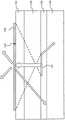
如果在用于光发射的限定的空间区域之外提供光阑,尤其是盘形状光阑,该光阑被设计成反射或吸收在界面处、尤其是在前层的前侧与周围环境之间的界面处反射回的光的至少一部分,则可以尤其有利地处理这种背反射。If a diaphragm, in particular a disk-shaped diaphragm, is provided outside the defined spatial region for light emission, the diaphragm is designed to reflect or absorb at the interface, in particular between the front side of the front layer and the surrounding environment Such back reflections can be handled particularly advantageously with at least a portion of the light reflected back at the interface.
此外,光阑可以防止背反射光从中间层进入后层并在装置的背面出射,即,通过后层和周围环境之间的界面。因此可以避免或减少来自装置后侧的不希望的光发射。In addition, the diaphragm prevents back-reflected light from entering the back layer from the intermediate layer and exiting at the back of the device, ie, through the interface between the back layer and the surrounding environment. Undesirable light emission from the rear side of the device can thus be avoided or reduced.
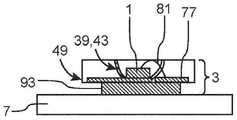
该光阑可以具有盘、尤其是圆形的和/或部分或多个部分的盘,该盘被布置在该后层的面向该中间层的表面上,其中该光源的后侧优选地被布置在该盘的中心。光阑可以是紧凑的和成本有效的。The diaphragm may have a disc, in particular a circular and/or partial or partial disc, which is arranged on the surface of the rear layer facing the intermediate layer, wherein the rear side of the light source is preferably arranged in the center of the disc. The diaphragm can be compact and cost effective.
在光源的前侧的平面图中,光源和限制装置可以覆盖盘的第一部分而不能覆盖位于径向方向外侧的盘的第二部分,其中从径向方向看,第二部分具有等于或大于2*D*0.84或2*D的宽度,其中D是前层的厚度。In a plan view of the front side of the light source, the light source and the confinement means may cover a first part of the disc but not a second part of the disc located outside in the radial direction, wherein the second part has a value equal to or greater than 2* as seen in the radial direction The width of D*0.84 or 2*D, where D is the thickness of the front layer.
因此,背反射,尤其是小角度的菲涅耳反射,可以经由光阑被吸收或反射。Thus, back reflections, especially small-angle Fresnel reflections, can be absorbed or reflected via the diaphragm.
因此,可以改善前向发射。可以减少或避免来自后侧的光辐射。Therefore, forward emission can be improved. Light radiation from the rear side can be reduced or avoided.
光阑可以具有穿孔盘,尤其是圆形和/或单件式或多件式的穿孔盘,其被布置成在光源上方并且在前层与后层之间居中。在限定的空间区域中发射的光可以通过穿孔盘的中心凹槽向前辐射,而向后反射的光被穿孔盘吸收或再次向前反射。The diaphragm may have a perforated disc, in particular a circular and/or single- or multi-part perforated disc, which is arranged above the light source and centered between the front and rear layers. The light emitted in the defined spatial area can be radiated forward through the central groove of the perforated disc, while the light reflected back is absorbed by the perforated disc or reflected forward again.
穿孔盘可以布置在远离光源的反射器或吸收器装置的周向端的水平处。穿孔盘的内边缘可以围绕和/或接触反射器或吸收器装置的远端。如在径向方向上看到的,穿孔盘可以具有等于或大于2*D*0.84或2*D的宽度,其中D是前层的厚度。背反射,尤其是菲涅耳反射,可以通过光阑被吸收或反射。The perforated disk may be arranged at a level remote from the circumferential end of the reflector or absorber arrangement of the light source. The inner edge of the perforated disk may surround and/or contact the distal end of the reflector or absorber device. As seen in the radial direction, the perforated disk may have a width equal to or greater than 2*D*0.84 or 2*D, where D is the thickness of the front layer. Back reflections, especially Fresnel reflections, can be absorbed or reflected by apertures.
光阑可以用作光源的至少一个电触点的至少一个电接触点。因此,可以经由光阑从光源的触点进行供电。光阑还可以被分成两个电分离的区域,使得光源的两个触点可以彼此独立地电接触。可替代地,该光阑的部分区域可以仅被提供为反射器或吸收器,而另一个部分区域实现了双重功能,因为它既被提供为电触点又被提供为反射器或吸收器。The diaphragm may serve as at least one electrical contact point for at least one electrical contact of the light source. Therefore, power can be supplied from the contacts of the light source via the diaphragm. The diaphragm can also be divided into two electrically separated regions, so that the two contacts of the light source can be in electrical contact independently of each other. Alternatively, a partial area of the diaphragm can be provided only as a reflector or absorber, while another partial area fulfills a dual function, since it is provided both as an electrical contact and as a reflector or absorber.
电气和/或电子驱动器装置可以在前层和后层之间横向地布置紧邻光源或在其下方。Electrical and/or electronic driver means may be arranged laterally between the front and rear layers immediately adjacent to or below the light source.
可替代地,驱动器装置可以布置在后层中。Alternatively, the driver device may be arranged in the rear layer.
驱动器装置的壳体可以设计成反射的或吸收的。The housing of the driver device can be designed to be reflective or absorbing.
光学装置可布置在光源的前侧,并设计成限制从光源发射的光的空间区域。为了改善光发射的前向方向性,可以在光源的前侧提供光学装置作为主光学器件。光学器件可以包括光子晶体结构或布拉格反射镜。例如,光子晶体结构或布拉格反射镜可以阻挡或减少在垂直于前侧法线的方向上的光传播。The optics may be arranged on the front side of the light source and designed to limit the spatial area of light emitted from the light source. In order to improve the forward directionality of the light emission, optics may be provided on the front side of the light source as primary optics. The optics may include photonic crystal structures or Bragg mirrors. For example, photonic crystal structures or Bragg mirrors can block or reduce light propagation in a direction perpendicular to the front side normal.
可以在后层的面向中间层的表面上或在后层中形成电布线层。也可以在后层中提供多个布线层。The electrical wiring layer may be formed on the surface of the rear layer facing the intermediate layer or in the rear layer. It is also possible to provide multiple wiring layers in the rear layer.
前层、后层和中间层可以层压在一起。为了平坦化,中间层可以具有层压板和/或填充材料,光源和其它部件例如限制装置被嵌入其中。层压材料可包括粘合剂或由粘合剂形成。中间层的材料可以具有与前层和后层的光学折射率相对应的光学折射率。The front layer, back layer and intermediate layer can be laminated together. For planarization, the intermediate layer may have a laminate and/or a filling material in which light sources and other components such as confinement means are embedded. The laminate may include or be formed from an adhesive. The material of the intermediate layer may have an optical index of refraction corresponding to the optical index of refraction of the front and rear layers.
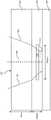
在一些实施例中,光电装置(尤其是显示装置)包括至少一个光电光源、至少部分透明的前层和至少部分透明的支撑层。该光源被布置在该前层与该支撑层之间,并且该光源的前侧面向该前层并且该光源的后侧面向该支撑层,并且其中在围绕该光源的周向方向上布置了限制装置。该限制装置被配置为用于限制光源发射光的空间区域,这样使得避免或至少减少了所发射的光的全内反射,尤其是在该前层与该外部之间的界面处的全内反射。这是有利的,因为例如可以在界面的照明和非照明区域之间获得改善的对比度。In some embodiments, an optoelectronic device, particularly a display device, includes at least one optoelectronic light source, an at least partially transparent front layer, and an at least partially transparent support layer. The light source is arranged between the front layer and the support layer, with the front side of the light source facing the front layer and the rear side of the light source facing the support layer, and wherein constraints are arranged in a circumferential direction around the light source device. The confinement means are configured to confine the spatial area of the light emitted by the light source such that total internal reflection of the emitted light is avoided or at least reduced, in particular at the interface between the front layer and the exterior . This is advantageous because, for example, an improved contrast can be obtained between the illuminated and non-illuminated areas of the interface.
该界面可以尤其地对应于光电装置的上表面。在装置是显示器的情况下,接口可以对应于显示器前侧。由于改善的对比度,可以增强观看显示器的用户的用户体验。This interface can correspond in particular to the upper surface of the optoelectronic device. Where the device is a display, the interface may correspond to the front side of the display. Due to the improved contrast, the user experience of the user viewing the display can be enhanced.
优选地,限制装置被配置为吸收光。限制装置例如可以具有黑色表面。可以相对于光源设计和布置限制装置,使得来自光源的将引起全内反射的光入射到限制装置上。因此这种光被吸收。Preferably, the confinement means are configured to absorb light. The limiting device can for example have a black surface. The confinement means can be designed and arranged relative to the light source such that light from the light source that would cause total internal reflection is incident on the confinement means. Therefore this light is absorbed.
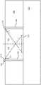
在一些实施例中,限制装置是环形元件,光电光源位于环形元件的内部,其中环形限制装置具有内径和高度,使得从光源发射的本来会在光电装置中、尤其是在前层和外层之间的界面处被全反射光被环形元件吸收。环形元件可以容易地制造,并且它可以用于减小由光源发射的光的角度范围。因此,可以避免以等于或大于全内反射临界角的入射角入射到界面上的光。In some embodiments, the confinement means is a ring-shaped element within which the optoelectronic light source is located, wherein the annular confinement means has an inner diameter and a height such that the emission from the light source would otherwise be in the optoelectronic device, especially between the front and outer layers. The totally reflected light at the interface between them is absorbed by the ring element. The annular element can be easily manufactured and it can be used to reduce the angular range of light emitted by the light source. Therefore, light incident on the interface at an incident angle equal to or greater than the critical angle of total internal reflection can be avoided.
光源优选地布置在环形元件内,使得环形元件的中心轴线与光源的中心重合。The light source is preferably arranged within the ring element such that the central axis of the ring element coincides with the center of the light source.
在一些实施例中,光电光源和环形元件位于中间层中。光电光源和环形元件可以布置在支撑层的与中间层相邻的表面上。In some embodiments, the optoelectronic light source and the ring element are located in the intermediate layer. The optoelectronic light source and the ring element can be arranged on the surface of the support layer adjacent to the intermediate layer.
支撑层例如可以是PET(聚对苯二甲酸乙二醇酯)层。中间层尤其可以是EVA(乙烯醋酸乙烯酯共聚物)或PVB(聚乙烯醇缩丁醛)层。前层可以是玻璃层。The support layer can be, for example, a PET (polyethylene terephthalate) layer. The intermediate layer may in particular be an EVA (ethylene vinyl acetate copolymer) or PVB (polyvinyl butyral) layer. The front layer may be a glass layer.
优选地,环形元件形成为环形形式,其在中间层中制成,尤其是通过激光钻孔制成,并且环形形式填充有吸收材料,例如黑色材料。这样的环形元件可以容易地和成本有效地制造。Preferably, the annular element is formed in an annular form, which is made in the intermediate layer, in particular by laser drilling, and the annular form is filled with an absorbing material, for example a black material. Such annular elements can be manufactured easily and cost-effectively.
光电光源可以布置在支撑层的背侧,并且限制装置可以布置在支撑层的顶侧。因此,限制装置和光源可以布置在支撑层的相对侧上。限制装置可以帮助减少相邻光源之间的串扰。The optoelectronic light source may be arranged on the back side of the support layer and the confinement means may be arranged on the top side of the support layer. Thus, the confinement means and the light source may be arranged on opposite sides of the support layer. Confinement devices can help reduce crosstalk between adjacent light sources.
该限制装置可以由至少一个结构化区域形成,该结构化区域包括吸收和/或部分或半透明材料并且被布置在该支撑层的顶侧上。The confinement means may be formed by at least one structured region comprising absorbent and/or partially or translucent material and arranged on the top side of the support layer.
光电光源可以由环形元件形成,尤其是由在支撑层的顶侧上的吸收和/或部分或半透明材料层部分制成。环形元件的中心轴线可以至少近似地与光电光源的中心轴线重合。The optoelectronic light source can be formed by a ring-shaped element, in particular by an absorbing and/or partial or semitransparent material layer portion on the top side of the support layer. The central axis of the annular element may at least approximately coincide with the central axis of the optoelectronic light source.
这种环形元件可以例如通过在支撑层的顶侧上提供吸收和/或部分或半透明材料的圆形元件来制造。中心圆形区域可以例如通过蚀刻、激光烧蚀或机械工艺从圆形元件去除,以获得环形元件。Such annular elements can be produced, for example, by providing circular elements of absorbing and/or partially or translucent material on the top side of the support layer. The central circular area can be removed from the circular element, eg by etching, laser ablation or mechanical processes, to obtain a ring-shaped element.
本发明还涉及一种光电装置、尤其是显示装置,其包括至少一个光电光源、至少部分透明的前层和至少部分透明的支撑层。光源布置在支撑层上或至少部分地嵌入在支撑层中。光源的前侧、面向前层,光源的后侧面向支撑层。在前层和支撑层之间布置部分或半透明的中间层,例如具有15%至25%或约18%的透射率。中间层可以有效地衰减在光电装置内传播的光,尤其是由于在光电装置的层之间的界面上或在光电装置的前侧和外部的界面上的不期望的反射。中间层例如可以是着色PVB层。The invention also relates to an optoelectronic device, in particular a display device, comprising at least one optoelectronic light source, an at least partially transparent front layer and an at least partially transparent support layer. The light source is arranged on the support layer or at least partially embedded in the support layer. The front side of the light source faces the front layer, and the rear side of the light source faces the support layer. A partially or translucent intermediate layer is arranged between the front layer and the support layer, eg having a transmittance of 15% to 25% or about 18%. The intermediate layer can effectively attenuate light propagating within the optoelectronic device, especially due to undesired reflections at the interface between the layers of the optoelectronic device or at the interface of the front side and the exterior of the optoelectronic device. The intermediate layer can be, for example, a pigmented PVB layer.
在一些实施例中,具有光散射元件的结构层布置在前层上。结构层可以是在光源上居中的层段。In some embodiments, a structural layer with light scattering elements is disposed on the front layer. The structural layer may be a layer segment centered on the light source.
在一些实施例中,中间层可以布置在前层和支撑层之间,并且具有光散射元件的结构层可以布置在前层和中间层之间。结构化散射层可以散射由光源提供的光,并因此提供前层和外部之间的界面的更均匀的照明。此外,以大入射角向界面传播并将在内部反射的光可被结构化散射层散射。然后,散射光可以以较低的入射角入射到界面上。因此,可以避免或减少界面处的全内反射。In some embodiments, an intermediate layer may be disposed between the front layer and the support layer, and a structural layer with light scattering elements may be disposed between the front layer and the intermediate layer. The structured scattering layer can scatter the light provided by the light source and thus provide more uniform illumination of the interface between the front layer and the exterior. In addition, light propagating towards the interface at large angles of incidence and reflecting internally can be scattered by the structured scattering layer. The scattered light can then be incident on the interface at a lower angle of incidence. Therefore, total internal reflection at the interface can be avoided or reduced.
在一些实施例中,部分或半透明的背层(也称为后层),例如透射率为15%至25%或约18%,布置在支撑层下方。例如由于在顶层和外部之间的界面处的全内反射,背层可以衰减通过层传播的不希望的光。或者,部分或半透明的后或背层可具有10%至90%或约20%的透射率。后层以及在前层与支撑层之间的中间层可具有不同的透射率值。例如,这些层可以不同地着色。In some embodiments, a partially or translucent back layer (also referred to as a back layer), eg, having a transmittance of 15% to 25% or about 18%, is disposed below the support layer. The back layer can attenuate unwanted light propagating through the layer, eg due to total internal reflection at the interface between the top layer and the exterior. Alternatively, the partially or translucent back or back layer may have a transmittance of 10% to 90% or about 20%. The rear layer and the intermediate layer between the front layer and the support layer may have different transmittance values. For example, the layers can be colored differently.
中间层可以布置在前层和支撑层之间,并且光电光源可以布置在支撑层上,其中中间层包括围绕光电光源或在光电光源上方的空腔,其中空腔填充有具有低折射率的材料,尤其是空气。An intermediate layer may be arranged between the front layer and the support layer, and the optoelectronic light source may be arranged on the support layer, wherein the intermediate layer comprises a cavity surrounding or over the optoelectronic light source, wherein the cavity is filled with a material having a low refractive index , especially air.
中间层可以布置在前层和支撑层之间,并且光电光源可以布置在支撑层上,其中中间层可以包括布置在光电光源上方的多个柱,其中柱可以包括具有低折射率的材料,尤其是空气。The intermediate layer may be arranged between the front layer and the support layer, and the optoelectronic light source may be arranged on the support layer, wherein the intermediate layer may comprise a plurality of pillars arranged above the optoelectronic light source, wherein the pillars may comprise a material having a low refractive index, in particular is air.
光电光源可以是LED或μLED(LED表示发光装置,μLED表示micro-LED)或mini LED或LED芯片或μLED芯片或mini LED芯片。The optoelectronic light source can be an LED or a μLED (LED means light emitting device, μLED means micro-LED) or mini LED or LED chip or μLED chip or mini LED chip.
LED可以例如具有150-200μm量级的边缘长度或小于300μm、尤其是小于150μm的边缘长度。The LEDs can, for example, have an edge length of the order of 150-200 μm or an edge length of less than 300 μm, in particular less than 150 μm.
LED或μLED或mini LED可以包括LED芯片或μLED芯片或mini LED芯片和/或包覆模制件和/或壳体。光电光源还可以是LED芯片或μLED芯片或mini LED芯片,并且不能包括包覆模制件和壳体。因此LED或μLED或mini LED可以是无壳体的。LED芯片或μLED芯片或miniLED可以包括用于向芯片提供驱动电流的电触点。The LED or μLED or mini LED may comprise an LED chip or μLED chip or mini LED chip and/or an overmold and/or a housing. The optoelectronic light source can also be an LED chip or a μLED chip or a mini LED chip, and cannot include an overmold and a housing. Thus LEDs or μLEDs or mini LEDs can be caseless. The LED chip or μLED chip or miniLED may include electrical contacts for providing drive current to the chip.
LED尤其地可以被称为mini LED,其是例如具有小于200μm、尤其地低至小于40μm、尤其地在200μm至10μm的范围内的边缘长度的小LED。另一个范围在150-40μm之间。然而,LED也可以称为micro LED,也称为μLED或μLED芯片、尤其是对于边缘长度在100μm至10μm范围内的情况。LEDs may in particular be referred to as mini LEDs, which are small LEDs, for example, having an edge length of less than 200 μm, in particular down to less than 40 μm, in particular in the range of 200 μm to 10 μm. Another range is between 150-40 μm. However, LEDs can also be called micro LEDs, also called μLEDs or μLED chips, especially for edge lengths in the range of 100 μm to 10 μm.
mini LED或μLED芯片可用作光电光源。mini LED或μLED芯片可形成像素或子像素并发射选定颜色的光。在一些实施例中,mini LED或μLED芯片可以是未封装的半导体芯片。Mini LED or μLED chips can be used as optoelectronic light sources. Mini LED or μLED chips can form pixels or sub-pixels and emit light of a selected color. In some embodiments, the mini LED or μLED chips may be unpackaged semiconductor chips.
在一些实施例中,每个光电光源可以包括被配置为发射选定颜色的光的mini LED或μLED芯片。在一些实施例中,每个光电光源可以包括一个或多个mini LED或μLED芯片,例如RGB像素,其包括三个mini LED或μLED芯片。RGB像素例如可以发射红色、绿色和蓝色以及任何混合颜色的光。In some embodiments, each optoelectronic light source may include a mini LED or μLED chip configured to emit light of a selected color. In some embodiments, each optoelectronic light source may include one or more mini LED or μLED chips, such as an RGB pixel, which includes three mini LED or μLED chips. RGB pixels, for example, can emit red, green, and blue, and any mixed color.
在一些实施例中,RGB像素还可以包括一个或多个集成电路(IC),尤其是小型集成电路,例如微型集成电路(μIC)。In some embodiments, the RGB pixels may also include one or more integrated circuits (ICs), especially small integrated circuits, such as micro integrated circuits (μICs).
在一些实施例中,光电装置包含载体或载体层(也称为中间层、第一层、第一层段或支撑层)以及前层和后层(也称为覆盖层和/或背层)。载体层可以布置在前层和后层之间。该载体层可以承载该至少一个光电光源或光电检测器,或者该至少一个光电光源或光电检测器可以部分地或完全地嵌入该载体层中。In some embodiments, the optoelectronic device comprises a carrier or carrier layer (also referred to as an intermediate layer, first layer, first layer segment or support layer) and front and back layers (also referred to as capping and/or backing layers) . The carrier layer can be arranged between the front layer and the rear layer. The carrier layer may carry the at least one optoelectronic light source or photodetector, or the at least one optoelectronic light source or photodetector may be partially or fully embedded in the carrier layer.
在一些实施例中,载体层可以是至少部分透明的,并且包括或由以下材料组成,例如高级或低级聚对苯二甲酸乙二醇酯(PET)、聚萘二甲酸乙二醇酯(PEN)、聚碳酸酯(PC)、(无色)聚酰亚胺(PI)、聚氨酯(PU)、聚(甲基丙烯酸甲酯)(PMMA)、多环芳烃(PAK)或任何其他合适的材料。尤其地,载体层可以包括或由至少部分透明的塑料、尤其是至少部分透明箔、尤其是柔性箔组成。In some embodiments, the carrier layer may be at least partially transparent and include or consist of materials such as high or low grade polyethylene terephthalate (PET), polyethylene naphthalate (PEN) ), polycarbonate (PC), (colorless) polyimide (PI), polyurethane (PU), poly(methyl methacrylate) (PMMA), polycyclic aromatic hydrocarbons (PAK) or any other suitable material . In particular, the carrier layer can comprise or consist of an at least partially transparent plastic, in particular an at least partially transparent foil, in particular a flexible foil.
前层和后层中的每一个可以由玻璃材料、塑料材料和/或任何其它合适的材料制成。前层和后层中的每一层可以仅含有一层或若干层相同或不同的材料。Each of the front and back layers may be made of glass material, plastic material and/or any other suitable material. Each of the front and back layers may contain only one or several layers of the same or different materials.
在一些实施例中,光电装置进一步包含至少一个辅助层,其也称为另外的层、中间层或旋转涂布玻璃(SOG)层。第一辅助层可以布置在载体层和前层之间,并且可选地,第二辅助层可以布置在载体层和后层之间。In some embodiments, the optoelectronic device further comprises at least one auxiliary layer, also referred to as an additional layer, interlayer, or spin-on-glass (SOG) layer. The first auxiliary layer may be arranged between the carrier layer and the front layer, and optionally, the second auxiliary layer may be arranged between the carrier layer and the rear layer.
该至少一个辅助层可以由以下项之一形成:The at least one auxiliary layer may be formed of one of the following:
熔融材料层或layer of molten material or
粘合剂层、尤其是热熔粘合剂层,adhesive layers, especially hot melt adhesive layers,
树脂,例如乙烯乙酸乙烯酯(EVA)、聚乙烯醇缩丁醛(PVB),或离聚物基体系。Resins, such as ethylene vinyl acetate (EVA), polyvinyl butyral (PVB), or ionomer based systems.
在一些实施例中,至少一个辅助层可将载体层包封在同一层中。该至少一个辅助层可以具有与该载体层相同的高度,然而该至少一个辅助层还可以具有与该载体层的高度不同的、尤其是更大的高度。该至少一个辅助层不仅可以在周向方向上包围该载体层,因为该载体层可以完全嵌入该至少一个辅助层中。In some embodiments, at least one auxiliary layer can encapsulate the carrier layer in the same layer. The at least one auxiliary layer can have the same height as the carrier layer, however, the at least one auxiliary layer can also have a height different from that of the carrier layer, in particular a greater height. The at least one auxiliary layer can not only surround the carrier layer in the circumferential direction, since the carrier layer can be completely embedded in the at least one auxiliary layer.
在一些实施例中,该至少一个辅助层可以是至少部分透明的。在一些实施例中,至少一个辅助层可以被黑化,得到至少部分透明的辅助层。如果光电装置包括多于一个的辅助层,则没有辅助层、一个辅助层、选定辅助层或所有的辅助层可被黑化。In some embodiments, the at least one auxiliary layer may be at least partially transparent. In some embodiments, at least one auxiliary layer may be blackened, resulting in an at least partially transparent auxiliary layer. If the optoelectronic device includes more than one auxiliary layer, no auxiliary layer, one auxiliary layer, selected auxiliary layers, or all auxiliary layers may be blackened.
在一些实施例中,该至少一个光电光源(尤其是LED)可以小于300μm、尤其是小于150μm。利用这些空间扩展,至少一个光电光源对于人眼几乎不可见。In some embodiments, the at least one optoelectronic light source (in particular an LED) may be smaller than 300 μm, in particular smaller than 150 μm. With these spatial expansions, at least one electro-optical light source is barely visible to the human eye.
在一些实施例中,至少一个光电光源是LED。LED可以尤其地称为mini LED,其是例如边缘长度小于200μm、尤其地小至小于40μm、尤其地在200μm至10μm的范围内的小型LED。另一个范围在150μm至40μm之间。In some embodiments, the at least one optoelectronic light source is an LED. LEDs may in particular be referred to as mini LEDs, which are eg small LEDs with an edge length of less than 200 μm, especially as small as less than 40 μm, especially in the range from 200 μm to 10 μm. Another range is between 150 μm and 40 μm.
LED也可以称为micro LED,也称为μLED或μLED芯片,尤其是对于边缘长度在100μm至10μm范围内的情况。在一些实施例中,LED可以具有90×150μm的空间尺寸,或者LED可以具有75×125μm的空间尺寸。LEDs can also be called micro LEDs, also called μLEDs or μLED chips, especially for edge lengths in the range of 100 μm to 10 μm. In some embodiments, the LED may have a spatial dimension of 90 x 150 μm, or the LED may have a spatial dimension of 75 x 125 μm.
在一些实施例中,mini LED或μLED芯片可以是未封装的半导体芯片。未封装可以意味着芯片没有围绕其半导体层的壳体,例如未封装的半导体模。在一些实施例中,未封装可以意味着芯片不含任何有机材料。因此,未包装的装置不含在共价键合中含有碳的有机化合物。In some embodiments, the mini LED or μLED chips may be unpackaged semiconductor chips. Unencapsulated may mean that the chip does not have a housing around its semiconductor layer, such as an unencapsulated semiconductor die. In some embodiments, unencapsulated may mean that the chip does not contain any organic material. Therefore, the unpackaged device does not contain organic compounds that contain carbon in covalent bonding.
在一些实施例中,每个光电光源可以包括被配置为发射选定颜色的光的mini LED或μLED芯片。在一些实施例中,每个光电光源可以包括一个或多个mini LED或μLED芯片,例如RGB像素,其包括三个mini LED或μLED芯片。RGB像素例如可以发射红色、绿色和蓝色以及任何混合颜色的光。In some embodiments, each optoelectronic light source may include a mini LED or μLED chip configured to emit light of a selected color. In some embodiments, each optoelectronic light source may include one or more mini LED or μLED chips, such as an RGB pixel, which includes three mini LED or μLED chips. RGB pixels, for example, can emit red, green, and blue, and any mixed color.
在一些实施例中,RGB像素还可以包括一个或多个集成电路(IC),尤其是小型集成电路,例如微型集成电路(μIC)。In some embodiments, the RGB pixels may also include one or more integrated circuits (ICs), especially small integrated circuits, such as micro integrated circuits (μICs).
在一些实施例中,光电装置包括至少一个导体线(也称为导电材料层元件)或接合线,且优选地包括两个导体线,以尤其是向至少一个光电光源供应电能和/或数据信号。In some embodiments, the optoelectronic device comprises at least one conductor wire (also referred to as a layer element of conductive material) or bond wire, and preferably two conductor wires, to supply power and/or data signals, in particular to the at least one optoelectronic light source .
在一些实施例中,载体层承载至少一个导体线。然而,在一些实施例中,至少一个辅助层可以承载至少一个导体线。In some embodiments, the carrier layer carries at least one conductor wire. However, in some embodiments, at least one auxiliary layer may carry at least one conductor wire.
在一些实施例中,该至少一个导体线可以是导电材料,例如铜。该至少一个导体线可以被涂覆和/或黑化以降低该至少一个导体线的外表面区域的反射率。涂层可以是例如钯或钼涂层。在一些实施例中,该至少一个导体线可以具有在5μm至50μm之间的范围内的宽度。In some embodiments, the at least one conductor wire may be a conductive material, such as copper. The at least one conductor wire may be coated and/or blackened to reduce the reflectivity of the outer surface area of the at least one conductor wire. The coating can be, for example, a palladium or molybdenum coating. In some embodiments, the at least one conductor line may have a width in a range between 5 μm and 50 μm.
在一些实施例中,该至少一个导体线可以形成为导电网,尤其是金属网。网可以被涂覆和/或黑化,尤其是为了降低导电网的外表面区域的反射率。涂层可以是例如钯或钼涂层。In some embodiments, the at least one conductor wire may be formed as a conductive mesh, especially a metal mesh. The mesh may be coated and/or blackened, especially to reduce the reflectivity of the outer surface area of the conductive mesh. The coating can be, for example, a palladium or molybdenum coating.
在一些实施例中,光电装置包括层堆叠,其包括载体层以及前层和后层。载体层尤其是中间层,其布置在前层和后层之间。至少一个电子或光电元件,尤其是光电光源,布置在载体层上,并且层堆叠的至少一个层,优选地,层堆叠的所有层是至少部分透明的。层堆叠包括至少一个导电层,其布置在层堆叠的两个相邻层之间或嵌入在层中。In some embodiments, an optoelectronic device includes a layer stack including a carrier layer and front and back layers. The carrier layer is in particular an intermediate layer, which is arranged between the front layer and the rear layer. At least one electronic or optoelectronic element, in particular an optoelectronic light source, is arranged on the carrier layer, and at least one layer of the layer stack, preferably all layers of the layer stack, are at least partially transparent. The layer stack comprises at least one conductive layer, which is arranged between two adjacent layers of the layer stack or embedded in a layer.
在一些实施例中,至少一个导电层包括电连接到光电光源的接触焊盘的至少一个导电线。该至少一个导电层可以是良好的导电和导热材料,例如铜、银、金和铝。至少一个导电层,尤其是至少一个导电线可以被涂覆和/或黑化,以降低至少一个导电线的外表面区域的反射率。涂层可以是例如钯或钼涂层。在一些实施例中,该至少一条电线可以具有在5μm至50μm之间的范围内的宽度。In some embodiments, the at least one conductive layer includes at least one conductive line electrically connected to the contact pads of the optoelectronic light source. The at least one electrically conductive layer may be a good electrically and thermally conductive material such as copper, silver, gold and aluminum. The at least one conductive layer, in particular the at least one conductive line, may be coated and/or blackened to reduce the reflectivity of the outer surface area of the at least one conductive line. The coating can be, for example, a palladium or molybdenum coating. In some embodiments, the at least one wire may have a width in a range between 5 μm and 50 μm.
该至少一个导电层可以包括导电网,例如金属网,尤其是铜网。网可以具有结点以及在结点之间的互连,其中,优选地,至少大部分互连不被中断。该至少一个导电层因此可以被结构化并且包括多个彼此连接的导线。The at least one conductive layer may comprise a conductive mesh, such as a metal mesh, especially a copper mesh. The net may have nodes and interconnections between the nodes, wherein preferably at least most of the interconnections are not interrupted. The at least one electrically conductive layer can thus be structured and comprise a plurality of wires connected to one another.
网状物可具有规则或不规则图案,其中不规则图案可为优选的,因为不规则图案可增加导电层的透明度。其原因可能是不规则图案可能更难以被人眼察觉。The mesh can have a regular or irregular pattern, with an irregular pattern being preferred because the irregular pattern can increase the transparency of the conductive layer. The reason for this may be that irregular patterns may be more difficult to detect by the human eye.
在一些实施例中,导电网被涂覆和/或黑化、尤其是用于降低导电网的外表面区域的反射率。涂层可以是例如钯或钼涂层。In some embodiments, the conductive mesh is coated and/or blackened, especially to reduce the reflectivity of the outer surface area of the conductive mesh. The coating can be, for example, a palladium or molybdenum coating.
如本文的光电装置的至少一些实施例可布置在非平坦或弯曲表面上,例如在交通工具或建筑物的外部或内部。这是尤其可能的,因为如本文的光电装置的至少一些实施例可基于柔性的层结构构建。At least some embodiments of optoelectronic devices as herein may be disposed on non-flat or curved surfaces, such as on the exterior or interior of vehicles or buildings. This is especially possible because at least some embodiments of optoelectronic devices as herein may be constructed based on flexible layer structures.
因此,本发明还涉及一种较大的实体,例如交通工具或建筑物,其在其外部或内部,尤其是在外部或内部表面上包括至少一个光电装置。Therefore, the invention also relates to a larger entity, such as a vehicle or a building, which comprises at least one optoelectronic device on its exterior or interior, especially on its exterior or interior surfaces.
借助于示例性实施例的描述并不将本发明限制于此。相反,本发明包括任何新的特征和特征的任何组合,其尤其地包括专利权利要求中的特征的任何组合,即使该特征或该组合本身没有在专利权利要求或示例性实施例中明确地陈述。The description with the aid of exemplary embodiments does not limit the invention thereto. Rather, the invention includes any novel feature and any combination of features, which in particular includes any combination of features in the patent claims, even if this feature or this combination itself is not expressly stated in the patent claims or the exemplary embodiments .
附图说明Description of drawings
附图的以下描述可以进一步说明和解释示例性实施例。功能相同或具有相同效果的部件由相同的附图标记表示。相同或实际上相同的部件可以仅参照它们首先出现的附图来描述。它们的描述不必在连续的图中重复。在附图中示出了:The following description of the accompanying drawings may further illustrate and explain exemplary embodiments. Components that have the same function or have the same effect are denoted by the same reference numerals. Identical or substantially identical parts may be described only with reference to the drawing in which they first appear. Their description need not be repeated in successive figures. In the attached drawing it is shown:
图1至图10是根据本发明的光电装置的不同实施例的示意性横截面视图,Figures 1 to 10 are schematic cross-sectional views of different embodiments of optoelectronic devices according to the present invention,
图11是在根据本发明的光电装置的载体中使用的示例性色彩的透射曲线图;11 is a transmission graph of exemplary colors used in a carrier of an optoelectronic device according to the present invention;
图12是根据本发明的光电装置的横截面和分解图;Figure 12 is a cross-sectional and exploded view of an optoelectronic device according to the present invention;
图13是图12的光电装置的局部横截面视图,Figure 13 is a partial cross-sectional view of the photovoltaic device of Figure 12,
图14是图12的光电装置的另一局部横截面视图,Figure 14 is another partial cross-sectional view of the photovoltaic device of Figure 12,
图15是图12的光电装置的另一局部横截面视图,Figure 15 is another partial cross-sectional view of the photovoltaic device of Figure 12,
图16是根据本发明的光电装置的横截面视图,Figure 16 is a cross-sectional view of a photovoltaic device according to the present invention,
图17是根据本发明的另一个光电装置的横截面视图,Figure 17 is a cross-sectional view of another photovoltaic device according to the present invention,
图18和图19用于说明根据本发明的制造光电装置的方法,18 and 19 are used to illustrate a method of manufacturing a photovoltaic device according to the present invention,
图20至图22用于说明根据本发明的制造另一光电装置的另一方法,20 to 22 are used to illustrate another method of fabricating another optoelectronic device according to the present invention,
图23和图24示出了在根据本发明的光电装置的一些实施例中用作电子线的阵列状结构的示例。Figures 23 and 24 show examples of array-like structures used as electron wires in some embodiments of optoelectronic devices according to the present invention.
图25是根据本发明的光电装置的示例性实施例的横截面侧视图;25 is a cross-sectional side view of an exemplary embodiment of an optoelectronic device according to the present invention;
图26是图25的装置的俯视图,Figure 26 is a top view of the device of Figure 25,
图27是根据本发明的光电装置的另一个示例性实施例的横截面侧视图,27 is a cross-sectional side view of another exemplary embodiment of an optoelectronic device according to the present invention,
图28是根据本发明的光电装置的另一个示例性实施例的横截面侧视图,28 is a cross-sectional side view of another exemplary embodiment of an optoelectronic device according to the present invention,
图29是图28的装置的俯视图,Figure 29 is a top view of the device of Figure 28,
图30是根据本发明的光电装置的另一个示例性实施例的横截面侧视图,30 is a cross-sectional side view of another exemplary embodiment of an optoelectronic device according to the present invention,
图31是图30的装置的俯视图,Figure 31 is a top view of the device of Figure 30,
图32是根据本发明的光电装置的另一个示例性实施例的横截面侧视图,32 is a cross-sectional side view of another exemplary embodiment of an optoelectronic device according to the present invention,
图33是图32的装置的俯视图,Figure 33 is a top view of the device of Figure 32,
图34是根据本发明的光电装置的另一个示例性实施例的横截面侧视图,34 is a cross-sectional side view of another exemplary embodiment of an optoelectronic device according to the present invention,
图35是图34的装置的俯视图,Figure 35 is a top view of the device of Figure 34,
图36是根据本发明的光电装置的另一个示例性实施例的横截面侧视图,36 is a cross-sectional side view of another exemplary embodiment of an optoelectronic device according to the present invention,
图37是图36的装置的俯视图,Figure 37 is a top view of the device of Figure 36,
图38是并非根据本发明的光电装置的横截面视图,Figure 38 is a cross-sectional view of a photovoltaic device not in accordance with the present invention,
图39是根据本发明的光电装置的第一变体的横截面视图,Figure 39 is a cross-sectional view of a first variant of an optoelectronic device according to the invention,
图40是根据本发明的光电装置的第二变体的横截面视图,Figure 40 is a cross-sectional view of a second variant of the photovoltaic device according to the invention,
图41是根据本发明的光电装置的第三变体的横截面视图,Figure 41 is a cross-sectional view of a third variant of the photovoltaic device according to the invention,
图42至图57是根据本发明的光电装置的不同变体的横截面视图,Figures 42 to 57 are cross-sectional views of different variants of optoelectronic devices according to the invention,
图58至图61是根据本发明的光电装置的另外的不同变体的横截面图,其中另外可以看到后层的截面,以及Figures 58 to 61 are cross-sectional views of further different variants of the optoelectronic device according to the invention, in which a cross-section of the rear layer can additionally be seen, and
图62至图65是根据本发明的光电装置的另外的不同变体的横截面图,其中另外可以看到前层的截面。Figures 62 to 65 are cross-sectional views of further different variants of the optoelectronic device according to the invention, in which a cross-section of the front layer can additionally be seen.
图66至图73示意性地示出了根据本发明的光电装置的不同变体的横截面侧视图。Figures 66 to 73 schematically show cross-sectional side views of different variants of optoelectronic devices according to the invention.
图74示意性地示出了根据本发明的光电装置的变体的俯视图。Figure 74 schematically shows a top view of a variant of an optoelectronic device according to the invention.
图75至图82示意性地示出了根据本发明的光电装置的不同变体的另外的横截面侧视图。Figures 75 to 82 schematically show additional cross-sectional side views of different variants of optoelectronic devices according to the invention.
具体实施方式Detailed ways
在图1的横截面视图中示出的光电装置包括配置为承载多个光电光源13的至少部分透明的载体层11。该装置还包括至少部分透明的覆盖层15。光源13布置在载体层11上。或者,它们可以至少部分地嵌入载体层11中(参见例如图4)。The optoelectronic device shown in the cross-sectional view of FIG. 1 includes an at least partially
每个光源13例如可以是LED,例如体积发射LED或表面发射LED。体积发射LED可以通过其顶表面和侧表面发射光,而表面发射LED可以通过其顶表面发射光。优选地,在如图1所示的实施例中,光源13是体积发射LED。Each
如图1所示的装置包括至少部分透明的中间层17,其布置在载体层11和覆盖层15之间。中间层17包括或由用于将载体层11粘合到覆盖层15的粘合剂组成。The device shown in FIG. 1 comprises an at least partially transparent
可以期望由光源13产生的光仅通过载体层11和覆盖层15之一射出,而不期望光通过另一层射出。为此,光电光源13可以被布置成使得由光源13产生的光通过载体层11或覆盖层15离开装置。通过“错误”层的出射应当是低水平或零水平。因此,光的发射可以是定向发射。It may be desirable for the light generated by the
如图1所示,每个光源13可以与反射光学元件19相关联,在此为曲面镜的形式。光学元件19嵌入载体层11中。光学元件19被配置为朝向载体层11反射由相关联的光电光源13发射的光,使得光通过载体层15离开装置(见图1中的箭头)。As shown in Figure 1, each
弯曲光学元件19可以具有形成反射表面的镜面涂层。涂层可以提供宽带反射率,包括在由光源13发射的光的波长区域中的反射率。或者,涂层的反射率对于发射光的波长或波长区域可以是选择性的。The curved
在一些实施例中,光源13可以被配置或布置为使得没有光发射通过上表面,即面向覆盖层15的光源13的表面。In some embodiments, the
如图2所示,光学元件19可以是光吸收或反射元件,尤其是平板形式的,其可以吸收从光电光源13向载体层11传播的光或将这种光反射回去,使得其通过覆盖层15出射。As shown in Figure 2, the
如图2所示的光学元件15布置在载体层11上,并且相关联的光电光源13布置在中间层17中的光学元件19的顶部上。光电光源13可以位于光学元件19的中心,如图2所示。The
如图2所示的光学元件19可以包括金属或者可以由多层反射镜制成。反射镜可以在宽的波长范围内反射,例如在400nm至800nm的范围内,或者在小的波长范围内反射,例如仅对420nm至480nm范围内的蓝光反射。
如图3所示,光电光源13可以布置在载体层11的面向覆盖层15的表面上(图3中未示出;覆盖层15在图3的光源上方)。光学元件19、尤其是反射或吸收光学元件,布置在载体层11的背离覆盖层15的相对表面上。例如,光学元件19由印刷在载体层11的表面上的涂层或结构形成。光学元件19可以包括基质材料,例如TiO2或ZrO2。光学元件19可以用作反射器,并且光学元件19可以至少部分地防止来自光源13的光可以通过光学元件19的外表面离开。As shown in FIG. 3 , the optoelectronic
光学元件19可以具有低于150μm的宽度或直径(在平行于载体层11的底表面的平面中测量)。The
如图4所示,光电装置的示例性实施例可包括第一组光电光源中的光电光源21。光源21可以布置成朝向载体层11的背离覆盖层15的表面(图4中未示出)发射光。覆盖层15在图4的装置中布置在载体层11之上,参见图1。此外,第二组光源中的光源23被布置为向载体层11的面向覆盖层15的表面发射光。As shown in FIG. 4, an exemplary embodiment of an optoelectronic device may include optoelectronic
第一组光源和第二组光源可以彼此独立地操作。第一组光源和第二组光源可以例如被布置成使得仅需要一个电导体线平面来向光源21、23提供电力并且控制光源21、23的操作。The first set of light sources and the second set of light sources may operate independently of each other. The first set of light sources and the second set of light sources may eg be arranged such that only one plane of electrical conductor wire is required to power the
第一组光源的光电光源21嵌入在载体层11中。第二组光源的光电光源23布置在载体层11上。光源21、23例如是倒装芯片,其在底表面上具有两个电接触焊盘25。光源21、23优选为通过其顶表面(即与底表面相对的表面)发射光的表面发射器。The optoelectronic
如图5所示,第一组光源的光电光源21和第二组光源的光电光源23都可以嵌入载体层11中。用于向光源23的接触焊盘25供电的电导体线27布置在光源23的外部,以从载体层11的表面向下到达光源23周围,从而接触这些接触焊盘25。因此,同样在图5的实施例中,单个平面的电导体线足以向光源21、23提供电力并控制光源21、23的操作。As shown in FIG. 5 , both the photoelectric
如图6所示,第一组光源的光电光源21和第二组光源的光电光源23可以布置在载体层11的相对表面上。可以通过布置在载体层11的相应表面上的至少一个电导体线的平面向光源21、23的接触焊盘25提供电。As shown in FIG. 6 , the optoelectronic
参考图4至图6,第一组光源的光源21、23和第二组光源的光源可以彼此独立地操作。因此,它们允许在载体层11的两侧上的电可调辐射分布。4 to 6, the
如图7所示,示例性光电装置可包括至少一个光成形元件29,这里为菲涅耳光学装置或菲涅耳透镜,其布置在单独的层31中并与布置在载体层11上和中间层17中的光电光源13对准。术语“光成形”应在广义上理解。尤其地,光成形元件29可以至少在一定程度上具有光束成形效果,因为它可以使光更多地在一个方向上发射。因此,光成形元件29可用于改善发射光的方向性。As shown in FIG. 7 , an exemplary optoelectronic device may include at least one light-shaping
在图8和图9的实施例中,光成形元件29是衍射光栅或全息膜。在图9的实施例中,包括光成形元件29的分离层31布置在覆盖层15和中间层17之间。In the embodiments of Figures 8 and 9, the
图7至图9的实施例可用作前灯或阅读灯,例如在交通工具的内部。衍射光栅和全息膜在波长上是选择性的。因此,它们可以适合于由光源13发射的光的波长。全息膜可以在其生产过程中曝光若干次,因此可以将其设置为对多个波长具有选择性。The embodiments of Figures 7 to 9 may be used as headlights or reading lights, eg in the interior of a vehicle. Diffraction gratings and holographic films are wavelength selective. Therefore, they can be adapted to the wavelength of the light emitted by the
载体层11优选为柔性载体层和/或由箔或玻璃材料制成。覆盖层15优选为柔性覆盖层,并且覆盖层15可以由玻璃或塑料材料如PMMA或PC制成。The
如图10所示,载体层11可以着色以减少或避免通过载体层11射出到外部的光。透射可以例如减小到所产生的光的强度的30%到35%范围内的强度。As shown in FIG. 10 , the
如图11所示,着色载体层11可以具有例如适合于光源13的发射曲线的透射曲线。因此,载体层11可以抑制在包括由光源13发射的光的波长的波长范围内的光透射。此外,它可以为室外视觉提供更高的透射率。As shown in FIG. 11 , the
如图12所示的光电装置包括:至少部分透明的中间层101,其例如是透明箔;以及多个光电光源103,诸如LED或μLED,其布置在中间层101上或嵌入中间层101中。The optoelectronic device shown in FIG. 12 comprises: an at least partially transparent
还如图13所示,光电装置还包括布置在中间层101的上表面107上的优选不透明的顶层105,例如有色箔。顶层105包括与光源103对准的多个孔口109,使得来自光源103的光可以通过与光源103对准的相应孔口109辐射到前部。As also shown in FIG. 13 , the optoelectronic device further comprises a preferably opaque
如图14所示,优选为中性密度过滤器的过滤层111布置在顶层105的上表面113上。过滤层可有助于改善光源的发射特性,尤其是关于亮度的均匀分布。As shown in FIG. 14 , a
此外,尤其参照图12和图15,不透明或至少部分透明的背景层115,例如有色箔,布置在中间层101的底表面117上。Furthermore, with particular reference to FIGS. 12 and 15 , an opaque or at least partially
光电装置可以以模块化方式构建,尤其是通过选择性地添加一个或多个上述层。因此,在一些实施例中,不是所有示出的层都可以存在。Optoelectronic devices can be constructed in a modular fashion, in particular by selectively adding one or more of the above-mentioned layers. Thus, in some embodiments, not all layers shown may be present.
这些层可以布置在不透明或至少部分透明的载体层125(见图15)和不透明或至少部分透明的覆盖层127(见图17)之间。如果存在背景层115,则载体层125可以布置在中间层101的底表面117上或背景层115的底表面119上。覆盖层127可以布置在过滤层111的上表面121上。These layers may be arranged between an opaque or at least partially transparent carrier layer 125 (see FIG. 15 ) and an opaque or at least partially transparent cover layer 127 (see FIG. 17 ). If
载体层125可以是透明的或部分透明的,例如,如果装置用于交通工具的窗户中。例如,如果装置布置在不透明表面上,例如在交通工具的内部或外部,则其可以是非透明载体层125。The
光电装置的所描绘的层可以是可弯曲的,从而提供一定程度的柔性。因此,这些层可以布置在例如交通工具的弯曲表面上。The depicted layers of the optoelectronic device may be bendable, thereby providing a degree of flexibility. Thus, these layers can be arranged, for example, on curved surfaces of vehicles.
顶层105具有与光源103对准的孔口109,使得朝向装置前侧的定向发射是可能的。The
相比于图12所示的装置,图16的光电装置具有背景层115,其具有与光源103对准的孔口109。因此,朝向装置背侧的定向光发射也是可能的。In contrast to the device shown in FIG. 12 , the optoelectronic device of FIG. 16 has a
在一些实施例中,如图17所示,顶层105不能具有孔口105,使得由于背景层115中的孔口109,仅朝向装置背侧的光发射是可能的。因此,装置可被配置为仅向前侧(图12)、仅向后侧(图17)或向两侧(图16)发射光。In some embodiments, as shown in FIG. 17 , the
如图16和图17进一步所示,相邻层可通过使用粘合剂或层压材料层123(例如热塑性层)彼此固定。As further shown in Figures 16 and 17, adjacent layers may be secured to each other through the use of an adhesive or a laminate layer 123 (eg, a thermoplastic layer).
如关于图18和图19,制造光电装置的一些实施例的方法包括提供至少部分透明的中间层101的步骤,尤其是透明箔,优选为如图18所示的平面带的形式。As with respect to Figures 18 and 19, methods of fabricating some embodiments of optoelectronic devices include the step of providing an at least partially transparent
该方法还包括在中间层101上提供多个光电光源103或将光源103嵌入中间层101中的步骤。The method also includes the step of providing a plurality of optoelectronic
此外,该方法包括在中间层103中产生多个光学元件129,例如微透镜的步骤,尤其是通过使用深拉工艺。光学元件129形成为与光源103对准。因此,光学元件129可以使关联光源103发射的光束成形,并且例如产生准直光束131或具有另一限定发射特性的光束。Furthermore, the method includes the step of producing a plurality of
通过关于图18和图19描述的制造方法获得的光电装置包括至少部分透明的中间层101、布置在中间层101上或嵌入中间层101中的多个光电光源103、以及多个光学元件129。每个光学元件129与光源103中的一个对准,并且光学元件129由于制造工艺而与中间层101一体地形成。The optoelectronic device obtained by the manufacturing method described in relation to FIGS. 18 and 19 comprises an at least partially transparent
图20至图22示出了制造根据本发明的光电装置的一些实施例的另一方法。该方法包括提供至少部分透明的中间层101,尤其是透明箔的步骤,其形式为如图20所示的平面带。该方法还包括在中间层101上提供多个光电光源103或将光源103嵌入中间层101中的步骤。通过使用例如深拉工艺,中间层101布置在弯曲的支撑表面(未示出)上。因此,中间层101也变成弯曲形状,如图21所示。20-22 illustrate another method of fabricating some embodiments of optoelectronic devices according to the present invention. The method includes the step of providing an at least partially transparent
每个光源103具有垂直于相应光源103的顶表面的表面法线133。如图21所示,使中间层101成为弯曲形状通常具有光源103的表面法线133彼此不平行的非希望效果。Each
如关于图22所示,光源103可以布置在平面中间层101上,使得在中间层101已经变成弯曲形状之后,光源103的表面法线133将彼此平行。附加地或替代地,光源103可以被布置成使得当中间层具有弯曲形状时,它们的表面法线133彼此等距地间隔开。图22所示的实施例提供了一个优点,即可以获得恒定的亮度,尤其是如果光源是朗伯发射器。As shown in relation to Figure 22, the
如前面关于图12所示的多层的模块化布置还可以包括一层或多层电线,其用于向光源提供电力(见图23和24)。电层可以由网格状或阵列状结构形成。网格状或阵列状结构可以例如被设计成类似于微型纱窗。该结构可以包括阵列状或网格状的段135,这些段彼此电和/或机械分离,如图23和图24中的分离线137所示。该分离可以例如通过使用激光切割由单件结构制成。The multi-layered modular arrangement as previously shown with respect to Figure 12 may also include one or more layers of electrical wiring for providing power to the light source (see Figures 23 and 24). The electrical layer may be formed of a grid-like or array-like structure. The grid-like or array-like structures can be designed to resemble miniature screens, for example. The structure may include an array or grid of
图23还示出了光电光源的接触焊盘(例如接触焊盘157)的示例性占用面积。在至少部分透明的光电装置中使用阵列状结构的这种段135可以有助于获得均匀的外观。此外,段135可以以即用状态提供,使得在光电装置的制造期间,它们可以直接布置在光电装置的其它层之间。Figure 23 also shows an exemplary footprint of contact pads (eg, contact pads 157) of the optoelectronic light source. The use of
图25和图26的光电装置包括布置在不透明载体层139的表面上的多个光电光源103,以及布置在载体层139的表面上在光电光源103和载体层139之间的反射和导电材料层141,尤其是金属层。The optoelectronic device of FIGS. 25 and 26 includes a plurality of optoelectronic
如图25所示,光电光源103可以可选地嵌入层159中。层159可以与光电光源103形成上平坦表面。层159可以是SOG层。此处,SOG可表示旋转涂布玻璃。层159可以包括散射由光源103发射的光的散射粒子。每个光电光源103具有一个电触点,这里是p触点,其位于光源103的底侧。底侧面向反射和导电材料层141。每个光电光源103底部的电触点接触反射和导电材料层141。因此,材料层141用作每个光电光源103的p触点的接触层。此外,材料层可以用作反射器,从而改善光源103相对于前向方向FD的辐射特性,其是背离材料层141的顶部表面的方向。As shown in FIG. 25 , the optoelectronic
每个光电光源103具有另一个电触点,这里是n触点,其位于光源103的顶侧。顶侧背离反射和导电材料层141。每个光电光源103的顶部处的电触点与布置在载体层139的表面上并与反射和导电材料层141分离的单独的接触焊盘143连接。由于使用了用于光源103的单独的接触焊盘143,所以可以单独地控制每个光源103。Each optoelectronic
在图25和图26所示的实施例中,光源是μLED,但它们也可以是LED。图25和图26所示的三个光源形成RGB像素。因此,光源之一被配置为发射红光,光源之一被配置为发射绿光,并且光源之一被配置为发射蓝光。这同样适用于下面参照图27至图37描述的实施例。In the embodiment shown in Figures 25 and 26, the light sources are μLEDs, but they could also be LEDs. The three light sources shown in Figures 25 and 26 form RGB pixels. Thus, one of the light sources is configured to emit red light, one of the light sources is configured to emit green light, and one of the light sources is configured to emit blue light. The same applies to the embodiments described below with reference to FIGS. 27 to 37 .
如图27所示,载体层139的表面可以包括多个空腔145。每个光源103布置在空腔145之一中。反射和导电材料层141尤其是完全覆盖空腔145的底表面、空腔145的侧壁表面和相邻空腔145之间的桥接部分147的顶表面。空腔145借助它们的载体层139的镜像顶表面可以改善光源103关于前向方向FD的辐射特性。尤其地,在横向方向上发射的光朝向前向方向FD向上反射。As shown in FIG. 27 , the surface of the
如图27所示,空腔145可以可选地填充有材料以形成相应的层159。层159可以与光电光源103一起形成平坦的上表面。层159可以是SOG层。层159可以包括散射由光源103发射的光的散射粒子。载体层139可以是至少部分透明的、透明的或不透明的。As shown in FIG. 27 , the
如图28和图29所示的光电装置包括布置在至少部分透明的载体层139的表面上的多个光电光源103,以及多个反射和导电材料层元件149,尤其是金属层元件。每个材料层元件149布置在载体层139的表面上并且在光电光源103之一和载体层139之间。材料层元件149的顶表面的面积大于关联光源103的底表面的面积,并且每个光源103在相关联的材料层元件149上居中。每个光电光源103具有一个电触点,这里是p触点,其位于光源103的底侧,使得其接触材料层元件149。每个材料层元件149还与接触焊盘151连接,这里是p接触焊盘。每个接触焊盘151可以处于相同的电势。The optoelectronic device shown in Figures 28 and 29 comprises a plurality of optoelectronic
每个光电光源103具有另一个电触点,这里是n触点,其位于光源103的顶侧。每个光电光源103的顶侧处的电触点与布置在载体层139的表面上并与反射和导电材料层元件149分开的单独的接触焊盘143连接。每个光电光源103的操作可以通过相关联的接触焊盘143来控制。因此,光源103的单独操作是可能的。Each optoelectronic
与光电装置的总表面积相比,光源103和电结构143、149、151的横截面尺寸较小。因此,如果装置的层结构是至少部分透明的,则光源103和电结构143、149、151不会或仅在很小程度上影响光电装置的透明度。此外,在图28和图29的装置中,在前向方向FD和后向方向BD上的光发射是可能的。横向发射也被接受。The cross-sectional dimensions of the
光源103可以嵌入层161中,该层可以与光源103一起形成平坦的上表面。层161例如可以是SOG层。在SOG层161之上布置可选的另一层163,其可以是散射层。层163可以包括散射粒子,其可以散射由光源103发射的光。The
图30和图31所示的实施例基于图28和图29的前述实施例。然而,非透明层153,尤其是黑色或深色层,布置在多个光电光源103上方的层中。非透明层153包括与光源103的顶表面对准的孔口,使得从光源103的顶表面发射的光可以通过孔口辐射。可选地,层153可以提供与接触焊盘143、151对准的孔口,如图31所示。在图30和图31的装置中,在前向方向FD和后向方向BD上的光发射是可能的。横向发射也被接受。The embodiments shown in FIGS. 30 and 31 are based on the previous embodiments of FIGS. 28 and 29 . However, a
如图30所示,光源103可以嵌入层165中,该层可以与光源103一起形成平坦的上表面。层165例如可以是SOG层。非透明层153布置在层165之上。载体层139优选是透明的。As shown in FIG. 30, the
图32和图33所示的实施例基于图28和图29的实施例。例如形成像素的三个光源103中的每一个的周围,在周向方向上布置例如以金属化小挖槽的形式的挡光器155。挡光器155可以为将光源103连接到接触焊盘143、151的电线提供通道。The embodiments shown in FIGS. 32 and 33 are based on the embodiments of FIGS. 28 and 29 . Around each of the three
如图32所示,光源103可以嵌入层167中,该层可以与光源103一起形成平坦的上表面。层167例如可以是SOG层。载体层139优选是透明的。As shown in FIG. 32, the
图34和图35的实施例基于图28和图29的实施例。图34和图35的实施例还包括透明或至少部分透明的载体层139,从而可以将光发射到前向方向FD和后向方向BD中。横向方向的光发射是可能的。然而,相邻光源103之间的距离使得沿横向方向发射的光可以被布置在光源103的层中的吸收器材料吸收。The embodiments of FIGS. 34 and 35 are based on the embodiments of FIGS. 28 and 29 . The embodiment of Figures 34 and 35 also includes a transparent or at least partially
如图34所示,光源103可以嵌入层169中,该层可以与光源103一起形成平坦的上表面。层169例如可以是SOG层。另一层171布置在层169之上。层171可以是散射层,并且它可以包括散射粒子。As shown in FIG. 34, the
图36和图37的实施例基于图28和图29的实施例。图36和图37的实施例被设计成通过减小p接触焊盘151的表面积和增大n接触焊盘143的表面积将光发射到后向方向BD中。设定表面积的比例,以便优化后向方向BD的发射。The embodiments of FIGS. 36 and 37 are based on the embodiments of FIGS. 28 and 29 . The embodiments of FIGS. 36 and 37 are designed to emit light into the backward direction BD by reducing the surface area of the p-
p接触焊盘151的表面积和n接触焊盘143的表面积也可以至少近似相等。因此,进入前向方向FD和后向方向BD的光发射可以至少近似相同,尤其是如果从光源103的层中的杂散光中心获得的杂散光以近似相同的量在前向和后向方向上发射。The surface area of p-
载体层139可以是透明的或部分透明的或半透明的。这同样适用于覆盖层175,该覆盖层可以是散射层并包括散射粒子。如图36所示,光源103可以嵌入另一层173中,其可以与光源103一起形成平坦的上表面,并且可以布置在覆盖层175下方。The
所有光源103可以是LED或μLED。光源103的高度,尤其是以μLED芯片的形式,可以是例如5μm。All
在图38中以横截面视图示出的非根据本发明的光电装置包括布置在例如LED、μLED、LED芯片或μLED芯片的中间层3中的光电光源1,例如由玻璃制成的至少部分透明的前层5,以及例如同样由玻璃制成的至少部分透明的后层7。中间层3还被设计为至少部分透明的,使得装置整体上至少部分透明。The optoelectronic device not according to the invention, shown in cross-sectional view in FIG. 38 , comprises an optoelectronic
光源1布置在前层5和后层7之间。在这种情况下,光源1可以被填充材料包围,使得中间层3至少大致是平面的。光源1的前侧9面向前层5,光源1的后侧11面向后层7。例如,后侧11可以布置在后层7的面对表面上。The
希望在光源1的前侧9上沿法线N的方向向前引导辐射。法线N还在前层5的前侧13上形成法线,该法线被提供作为装置的观察者的观察区域。然而,光源1通常将光发射到具有发射方向的空间区域中,其中发射方向也相对于法线N强烈倾斜。例如,光束15可以从光源1发射,其以相对小的入射角撞击在前侧13和周围环境之间的界面上。这里的入射角是指光束15的传播方向和法线N之间的角度。It is desired to direct the radiation forward in the direction of the normal N on the
光束15的绝大部分将根据光的折射定律通过界面17出射到周围环境中,如光束19所示。如光束21所示,根据反射定律反射一小部分光(在光学折射率n=1.5的玻璃到n=1的空气的转变处的强度的约4%)。这种反射在本文中也称为菲涅耳反射,因为可以通过本身已知的菲涅耳公式进行定量观察。A substantial portion of
如光束25所示,以等于或大于全反射临界角的角度入射在界面17上的光束23在从前层的光学密度较大的介质(例如,n=1.5的玻璃)到周围环境(大约n=1的空气)的过渡处被完全反射。As indicated by
尤其地,当光源1是体积发射器时,光束(比较光束27)也可以直接在由后层7和周围环境之间的界面31形成的装置的后侧29的方向上发射。与光束21类似,光束27也可以穿过界面31,使得相应的光束31、33在后侧29处出现。来自后侧29的这种光发射是不希望的。在界面31处的附加菲涅耳反射未示出。In particular, when the
背反射不仅可以发生在相邻界面17、31处,而且可以发生在内界面35、37处。内界面35位于中间层3和前层5之间。另外,第二内界面37位于中间层3和后层7之间。内界面35、37处的背反射可由例如层压产生。中间层3基本上由层压板形成,以便将前层5和后层7连接到位于其间的至少一个光源1。除了层压材料之外,粘合剂和/或填充材料也可以存在于中间层3中。这种背反射还可导致前侧13处的不期望的光发射。这些可能导致刺激、模糊或重影,这也是不希望的。Back reflections can occur not only at
图39中所示的根据本发明的光电装置的变体与图38的装置的不同之处尤其在于,其具有限制装置39,该限制装置限制光源1发射光到限定的空间区域的空间区域,参见光束41。尤其地,限制装置39具有反射器或吸收器装置43,其被设计为至少近似抛物线形状、反射或吸收带,并且在周向方向上完全围绕光源1或其发射区域周围的法线N延伸。The variant of the optoelectronic device according to the invention shown in FIG. 39 differs from the device of FIG. 38 in particular in that it has limiting means 39 which limit the emission of light from the
根据设计,反射器或吸收器43具有反射或吸收表面,并且被设计和布置成吸收或反射光源1在限定的空间区域之外辐射的光。反射尤其是以这样的方式发生,即反射光仅在限定的空间区域中传播,在图39的变体中,该限定的空间区域位于箭头41和法线N之间。这在图39中由光束45表示,该光束可以从前侧13作为可见像素出现,参照光束47。Depending on the design, the reflector or absorber 43 has a reflecting or absorbing surface and is designed and arranged to absorb or reflect light radiated by the
然而,限制装置39吸收或反射光束41,其将以一定角度入射到固定边界17上,该角度是从法线N测量的,等于或大于该边界17处全反射的临界角。如图38所示,通过使用限制装置39,可以避免在其它界面处引起进一步反射的全反射光束25。However, the confinement device 39 absorbs or reflects the
此外,根据图39的装置包括被设计成盘61的光阑49,根据该设计,该光阑被设计成反射或吸收光的至少一部分(参照光束51),该光的至少一部分在界面17、35处,尤其是在前侧13与周围环境之间的界面17处被反射回来。在所示的情况下,光阑49反射,使得光束51在光束53中反射,该光束作为光束55从前侧13出现。小的背反射部分,参照光束57,可导致光束59从背部29出射。Furthermore, the device according to FIG. 39 comprises a
然而,当n=1.5的玻璃用作前和后层5、7时,由于在界面17处发生两次反射,其强度约为光束45的初始强度的0.16%。因此,这在可接受的界限范围内。However, when glass with n=1.5 is used for the front and
为了吸收或反射尤其是在外界面17处的菲涅耳背反射,光阑49是圆形设计的并且具有相对于光源1和限制装置39的突起。在正面13的平面图中看,光源1和限制装置39覆盖了光阑49的第一部分,而在径向方向上看,光阑的第二部分未被覆盖。该第二部分具有至少近似一个环的横截面形状。该突起对应于第二部分在径向方向上的宽度B。优选地,宽度B等于或大于2*D*0.84或2*D,其中D是前层5的厚度。在这种情况下,沿法线N测量厚度D,并且径向方向垂直于法线N。因子0.84近似对应于40°的正切,其中40°近似对应于在从n=1.5的玻璃到n=1的空气的过渡处的全反射的临界角。In order to absorb or reflect Fresnel back-reflections, in particular at the
图40的装置的结构主要对应于图39的结构。然而,光阑设计成两部分。它包括例如圆盘61,该圆盘布置在后层7上并且光源1以居中的方式布置在其上。盘61可以是反射或吸收设计。由于盘61位于光源1的下面,它也可以不在功能上配置为反射器或吸收器,而是仅用作光源1的电触点的电接触点。在这种情况下,盘61也可以不被认为是光阑的元件,因为它不实现反射器或吸收器功能。The structure of the apparatus of FIG. 40 mainly corresponds to the structure of FIG. 39 . However, the diaphragm is designed in two parts. It comprises, for example, a
此外,光阑包括圆形穿孔盘或环形盘63,其中心凹槽65围绕反射器或吸收器43。穿孔盘63进而可以是反射或吸收设计。穿孔盘63的内边缘67接触反射器或吸收器43的远离光源1的端部。穿孔盘63因此位于光源1上方的中间层3中,并且更靠近位于光源1前方的界面17、35。结果,来自这些界面的背反射可以根据穿孔盘63的设计以改进的方式被吸收或反射。如果盘61仅用作电触点,则仅穿孔盘63可被视为光阑元件。Furthermore, the diaphragm comprises a circular perforated disk or
在径向方向上观察,穿孔盘63可以优选地具有等于或大于2*D*0.84或大于2*D的宽度B,其中D是前层5的厚度。Viewed in the radial direction, the
图41的装置与图39的装置的不同之处尤其在于限制装置39的设计,其占据光源1周围的体积区域71。低折射材料,例如空气,可以包含在体积区域71中。因此,在体积区域71和中间层3的周围介质之间的界面73处没有发生全反射,其可以具有例如1.5的折射率。The device of FIG. 41 differs from the device of FIG. 39 in particular in the design of the confinement device 39 , which occupies a volumetric area 71 around the
然而,在中间层3的周围介质中传播的光束由于介质的较高折射率而朝向法线N折射。因此,发射的空间区域变窄。结合体积区域的高度(相对于法线N的方向)和直径(相对于横向于法线的径向方向)的巧妙选择,可以实现没有离开体积区域71以全反射的临界角或以甚至更大的入射角入射到边界表面17上的光束。因此可以避免在外部界面17处的全反射。However, the light beam propagating in the surrounding medium of the
优选地,光阑49的突起再次具有等于或大于2*D*0.84或2*D的宽度B,其中D是前层5的厚度。Preferably, the protrusion of the
与图38的装置相比,图39至图41中所示的变体对于向前辐射具有改进的方向性。如所解释的,可以防止或避免背和/或全反射。因此,离开前侧13或后侧29的不希望的光束的强度可以至少减小。因此,减少了或不会出现不期望的效果,例如刺激、重影或模糊。Compared to the device of Figure 38, the variants shown in Figures 39 to 41 have improved directivity for forward radiation. As explained, back and/or total reflections can be prevented or avoided. Thus, the intensity of the undesired light beams leaving the
图42中部分示出的装置基于图39的变体。然而,光阑49被分开。中间第一区域75用作光源1下侧上的电触点的电接触点。在这种情况下,第一区域75也可以不具有反射器或吸收器特性,也就是说,它可以用作“经典的”电触点。The apparatus shown in part in FIG. 42 is based on the variant of FIG. 39 . However, the
相对于第一区域75径向最外面的第二区域77可以设计为反射器或吸收器,并且第二区域77可以通过接合线81连接到光源1的前侧9上的电触点。因此,第二区域77可以实现双重功能,并因此既用作电触点又用作光反射器或光吸收器。The radially outermost
此外,第三区域79可用作光反射器或光吸收器。光阑49整体上可具有圆形横截面。第二和第三区域77、79可以各自具有环形分段形状的横截面,其中这三个区域可以彼此电分离。其它横截面形状也是可能的。Additionally, the
接合线81可以被引导通过设置在反射器或吸收器装置43中的狭缝。The
图43的变体基于图40的变体。穿孔盘63具有两部分设计,其中第一穿孔盘段83不仅被设计成吸收或反射的,而且还可以用作位于前侧9上的光源1的电接触点的电接触点。接合线81连接两个接触点。The variant of FIG. 43 is based on the variant of FIG. 40 . The
此外,第二穿孔盘部分85可以设计成吸收或反射的,但不实现作为接触点的功能。两个穿孔盘段83、85彼此电隔离。Furthermore, the second
图44的变体基于图39的变体。光源1是所谓的倒装芯片,其中两个电接触点都位于下侧上。中间第一区域75和径向外部第二区域77可以实现双重功能,并且既用作反射器或吸收器,又用作倒装芯片的各个接触点的电接触点。The variant of FIG. 44 is based on the variant of FIG. 39 . The
此外,第三区域79可仅用作光反射器或光吸收器,而不用作电触点。三个区域75、77和79一起可具有圆形横截面,其中单独区域的横截面形状可适应(例如)于倒装芯片侧上的接触点的几何形状和布置。Furthermore, the
图45的变体基于图39的变体。盘61为两部分设计。第一子盘87和第二子盘89彼此电隔离。每个子盘87、89用作实现为倒装芯片的光源1的下侧上的相应接触点的电接触点。两个子盘87、89也可以可选地设计为反射或吸收的。The variant of FIG. 45 is based on the variant of FIG. 39 . The
图42至图46所示的变体尤其适合与设计为体积发射器的光源1结合使用。这里,光不仅在前侧9出射,而且在横向外侧出射。图42至图46的变体也可以与被设计为表面发射器的光源1组合使用。此处,光仅从前侧9射出。当使用这样的表面发射器时,反射器或吸收器43a也可以布置在前侧9上,并被向外和向上引导远离后者,如图45中通过虚线的示例所示。The variants shown in FIGS. 42 to 46 are particularly suitable for use in combination with
图46的变体基于图42的变体。用于改善前向方向性的光学装置91布置在光源1的前侧9上。光学装置91可以是例如光子晶体结构或布拉格反射镜。The variant of FIG. 46 is based on the variant of FIG. 42 . Optical means 91 for improving the forward directivity are arranged on the
图47的变体基于图43的变体。图48的变体基于图44的变体。图49的变体基于图45的变体。在图47至图49的变体中,如在图46的变体中,用于改进前向方向性的对应的光学装置91被布置在光源1的前侧9上。The variant of FIG. 47 is based on the variant of FIG. 43 . The variant of FIG. 48 is based on the variant of FIG. 44 . The variant of FIG. 49 is based on the variant of FIG. 45 . In the variant of FIGS. 47 to 49 , as in the variant of FIG. 46 , corresponding optical means 91 for improving the forward directivity are arranged on the
图50的变体基于图42的变体。在这种情况下,电或电子驱动器装置93优选地与集成电路一起布置,用于控制光阑49上,尤其是第三区域79上的光源1。The variant of FIG. 50 is based on the variant of FIG. 42 . In this case, electrical or electronic driver means 93 are preferably arranged together with an integrated circuit for controlling the
图51的变体基于图43的变体。图52的变体基于图44的变体。图53的变体基于图45的变体。在图51至图53的变体中,如在图50的变体中,布置了电气或电子驱动器装置93。在这种情况下,如图51所示,光源1下面的盘61的直径可以扩大,以便用作驱动器装置93的载体。The variant of FIG. 51 is based on the variant of FIG. 43 . The variant of FIG. 52 is based on the variant of FIG. 44 . The variant of FIG. 53 is based on the variant of FIG. 45 . In the variant of FIGS. 51 to 53 , as in the variant of FIG. 50 , electrical or electronic driver means 93 are arranged. In this case, as shown in FIG. 51 , the diameter of the
在图52中,驱动器装置93可位于第二和第三区域77、79上。In FIG. 52 , the
驱动器装置93可以部分地放置在第二子盘89上,如图53所示。各个驱动器电路93可以包括吸收或反射外壳(未示出)。The
图54的变体基于图42的变体。驱动器装置93布置在光源1的下面。光阑49可进而被分开,使得部分区域可被接合线81接触。The variant of FIG. 54 is based on the variant of FIG. 42 . The
图55的变体基于图43的变体。此处,驱动器装置93替换光源1下面的盘61。The variant of FIG. 55 is based on the variant of FIG. 43 . Here, the
图56的变体基于图44的变体。设计为倒装芯片的光源1放置在驱动装置93上,该驱动器装置进而放置在光阑49上。光阑49可以设计成单部分或多部分部件。The variant of FIG. 56 is based on the variant of FIG. 44 . The
图57的变体基于图45的变体。设计为倒装芯片的光源1放置在驱动器装置93上,该驱动器装置进而放置在盘61上。盘61可以可选地细分为两个子盘(参见图45中的子盘87、89)。The variant of FIG. 57 is based on the variant of FIG. 45 . The
图42至图57中所示的变体可以被平坦化,使得它们形成中间层(参见中间层3)并且在两侧例如用层压材料、粘合剂、硅酮、环氧树脂、聚酰亚胺粘合到前层和后层5、7。在这种情况下,可以首先发生与后层7或与前层5的接触。中间层3随后被平面化,然后施加仍然缺失的前层或后层。The variants shown in Figs. 42 to 57 can be planarized such that they form an intermediate layer (see intermediate layer 3) and on both sides for example with laminates, adhesives, silicones, epoxies, polyamides The imine is bonded to the front and
在图54至图57的变体的修改中,驱动器装置93可容纳在后层7中。在这种情况下,相对于从前侧13的俯视图,驱动器装置93可以位于光源1的后面。结果,由于不透明光源1和不透明驱动器装置93的已经较小的横截面重叠,可以提高装置的透明度。In a modification of the variant of FIGS. 54 to 57 , the
而且,一个或多个电布线层可以容纳在后层7(未示出)中。Also, one or more electrical wiring layers may be accommodated in the rear layer 7 (not shown).
图58的变体基于图42的变体。图59的变体基于图43的变体。图60的变体基于图44的变体。The variant of FIG. 58 is based on the variant of FIG. 42 . The variant of FIG. 59 is based on the variant of FIG. 43 . The variant of FIG. 60 is based on the variant of FIG. 44 .
图61的变体基于图45的变体。然而,在图58至图61的每个变体中,搁置在后层7上的驱动器装置93被布置在相应的光阑49或盘61下方。The variant of FIG. 61 is based on the variant of FIG. 45 . However, in each of the variants of FIGS. 58 to 61 , the
驱动器装置93形成中间层3的一部分。在附着到后层7并例如通过引入填充材料进行平面化之后,可以附着前层5。前层5可以例如通过层压材料、粘合剂、硅酮、环氧树脂或聚酰亚胺附着。The
图42至图61所示的变体也可以被视为结构元件(在图58至图61的变体中没有后层7)。在这种情况下,结构元件包括具有关联限制装置和/或关联光阑的光源1。在前层和后层5、7之间可以布置多个这种结构元件,尤其是阵列状的。中间层3中的自由空间可以例如用填充材料填充,使得中间层3可以形成为平坦的平坦化层。这样,例如,可以形成具有以阵列状方式布置的光源1的透明显示器。这样,例如,每个光源1可以形成一个像素。The variants shown in FIGS. 42 to 61 can also be considered as structural elements (without the
图62的变体基于图42的变体。图63的变体基于图43的变体。图64的变体基于图44的变体。The variant of FIG. 62 is based on the variant of FIG. 42 . The variant of FIG. 63 is based on the variant of FIG. 43 . The variant of FIG. 64 is based on the variant of FIG. 44 .
图65的变体基于图45的变体。在图62至图65的变体中,在它们的制造过程中,相应的结构元件首先被附接到前层5上,如图42至图45所示,该前层可以是一层或多层玻璃窗格。The variant of FIG. 65 is based on the variant of FIG. 45 . In the variants of FIGS. 62 to 65 , during their manufacture, the corresponding structural elements are first attached to the
为了形成完整的中间层3,例如可以用填充材料填充剩余的自由空间,使得在附着图62至图65中未示出的下层7之前存在平坦化的中间层3。粘合可以例如用层压材料、粘合剂、硅酮、环氧树脂或聚酰亚胺进行。In order to form the complete
为了将结构元件紧固到前层5上,这些结构元件可以被多个吸收块95包围,这些吸收块例如是长方体。块95可以在其下侧和侧边缘上围绕相应的结构元件。尽管其中光从结构3射出的限定的空间区域没有被覆盖,这些块也可以布置在与前窗格5的界面35处。通过块95,相应的结构可以以简单且成本有效的方式连接到前层5。此外,块95可以防止或减少相邻光源之间的不期望的光学相互作用。In order to fasten the structural elements to the
如以上已经解释的,在每种情况下示出的变体仅示出了具有相关联的限制装置和/或光阑的一个光源1。这些可以被认为是结构元件。具有相应光源1的多个这样的结构元件可以设置在相应的中间层3中,该中间层可以例如以阵列状方式布置。每个光源1可以被认为是阵列状排列的像素。As already explained above, the variants shown in each case show only one
每个光源1也可以发射红色、绿色或蓝色之一的光。在每种情况下,具有不同颜色的3个光源可以形成像素。由此可以形成RGB显示器。一种颜色的每个光源1优选地具有相关联的限制装置和/或相关联的光阑。Each
前和后层5、7优选为玻璃,其可以设计为一层或多层。The front and
如图66所示的光电装置包括布置在至少部分透明的支撑层103上的一个或多个光电光源101。至少部分透明的前层(例如玻璃层)布置在一个或多个光电光源101上方。一个或多个光电光源101位于中间层105中,该中间层位于支撑层103和前层之间。支撑层103可以是PET(聚对苯二甲酸乙二醇酯)层,中间层105可以是EVA(乙烯醋酸乙烯酯共聚物)或PVB(聚乙烯醇缩丁醛)层。The optoelectronic device shown in FIG. 66 includes one or more optoelectronic
前层包括到外部的界面,其通常是空气。该界面尤其地由玻璃层的上表面形成(图66中未示出)。尤其地,该界面处,如果光的入射角等于或大于临界角,则来自光电光源101的光可在内部全反射。临界角是产生全内反射的最小入射角。相对于表面法线测量入射角。The front layer includes the interface to the outside, which is usually air. This interface is formed in particular by the upper surface of the glass layer (not shown in Figure 66). In particular, at this interface, if the incident angle of the light is equal to or greater than the critical angle, the light from the photoelectric
为了避免在界面处发生全内反射,在围绕光源101的周向方向上提供限制装置107。如果存在多于一个的光源101,则它们通常彼此间隔开,使得可以围绕每个光源101布置单独的限制装置107。In order to avoid total internal reflection at the interface, limiting means 107 are provided in the circumferential direction around the
如图66所示,限制装置107可以具有环形元件109的形式,并且其尺寸可以设置成限制来自光源101的光可以在其中传播的空间区域111。图66示出了来自光源101的两个光束113、115,它们正好不被限制装置107阻挡,因为它们可以正好通过环形限制装置109的上内边缘117。因此,光束113、115至少近似地在限制装置107之后显现光的发射锥的外边界。As shown in Figure 66, the confinement means 107 may have the form of a ring-shaped
环形元件109被配置为限制来自光源101的光可以在其中传播的空间区域111,从而避免或至少减少全内反射。因此,避免或至少减少了由于界面处的全内反射而在装置中传播的不希望的光束。由此可以增强界面上的颜色对比度。此外,尤其是在单色应用中和/或在包括不同颜色的应用中,可以改善界面上的亮度对比度。The
环形元件109优选包括吸收表面。例如,它可以由黑化的金属结构制成。例如,它可以由具有附加黑化的电镀铜形成。它也可以由覆盖有黑色涂层的抗蚀剂,尤其是透明抗蚀剂形成。或者,其可由具有高纵横比的印刷结构形成。The
在图66的示例中,优选为μLED的光源101具有50μm的边缘长度,并且环形元件109具有55μm的宽度和55μm的高度。In the example of Figure 66, the
图67所示的光电装置与图66的变体的不同之处在于,优选为μLED的光源101具有20μm的边缘长度,并且环形元件109具有50μm的宽度和50μm的高度。The optoelectronic device shown in FIG. 67 differs from the variant of FIG. 66 in that the
图68所示的光电装置与图66的变体的不同之处在于,优选为μLED的光源101具有20μm的边缘长度,并且环形元件109具有35μm的宽度和35μm的高度。The optoelectronic device shown in FIG. 68 differs from the variant of FIG. 66 in that the
图69所示的光电装置与图66的变体的不同之处在于,环形元件109由环形形式构成,该环形形式例如通过激光钻孔形成在中间层105中,并且填充有吸收材料。The optoelectronic device shown in FIG. 69 differs from the variant of FIG. 66 in that the
或者,在中间层105中已经形成环形形式之后或通过将这种结构压入中间层105中,可以将由吸收或黑色材料覆盖的预结构化金属装置嵌入中间层105中(图69中未示出)。Alternatively, a prestructured metal device covered by an absorbent or black material can be embedded in the
与前面的示例相比,在图70的光电装置中,光源101布置在支撑层103的背侧119上,而限制装置107布置在支撑层103的顶侧121上。此外,限制装置103由吸收和/或部分或半透明材料的平坦表面区域123形成。In contrast to the previous example, in the optoelectronic device of FIG. 70 , the
在图70所示的示例中,表面区域123可以具有环的形式。相应的环形元件125的中心轴线127至少近似地与光电光源101的中心轴线129重合。In the example shown in Figure 70, the
环形元件125的中心开口131可以限制来自光源101的光可通过开口131传播的空间区域111。尤其地,开口131的尺寸可以被确定为使得可以避免或至少减少光在前层和外部(图70中未示出)之间的界面处的全内反射。因此,在图70的装置中可以避免或减少由于界面处的全内反射而在装置中传播的不希望的光束。此外,环形元件125可以帮助减少不同光源101(图70中未示出)之间的串扰。The
具有中心开口131的环形元件125可以由经涂覆的圆形层形成。此外,可以从圆形层去除层材料以获得中心开口131。这种去除可以例如通过蚀刻工艺、机械工艺或激光烧蚀来进行。圆形层和相应的环形元件125可以由至少部分透明的层制成,例如着色层。The
图71所示的光电装置包括至少一个光电光源101、至少部分透明的前层133、至少部分透明的支撑层103和中间层105。支撑层103可以是PET(聚对苯二甲酸乙二醇酯)层,中间层105可以是EVA(乙烯醋酸乙烯酯共聚物)或PVB(聚乙烯醇缩丁醛)层,前层133可以是玻璃层。中间层105可以具有0.76mm的高度,并且前层133可以具有2.1mm的高度。The optoelectronic device shown in FIG. 71 includes at least one optoelectronic
光源101至少部分地嵌入支撑层103中。光源101的前侧面向前层133,光源101的后侧面向支撑层103。光源101优选为表面发射光电光源,其在其前侧发射光。然而,至少在一些实施例中,光源101也可以是体积发射光电光源。The
图71示出了可能由光源101发射的光束135、137、139、141。光束139是垂直于各层传播的光束,因此以至少约零度的角度(从表面法线的角度看)入射到前层133和外部之间的界面143上。由于界面143处折射率的变化,该光束的一小部分(相对于光束的强度)可能被反射。相反,光束135、137、141以大入射角入射到界面143上。如果入射角等于或大于全反射的临界角,则光束135、137、141的全部强度被反射回去。FIG. 71 shows the light beams 135 , 137 , 139 , 141 that may be emitted by the
中间层105是部分透明或半透明的。例如,中间层105可以具有大约18%的透射率。该层的透射率由透射辐射功率与入射辐射功率之比定义。18%的值仅仅是一个示例。在另一个示例中,该值可以在15%至25%的范围内。由于中间层105的低透射率,层133、105、103中的反射光(来自“正常”菲涅耳反射或来自全内反射)的传播可以被衰减和减少。The
图72所示的光电装置与图71的实施例的不同之处在于散射层145布置在前层133和中间层105之间。散射层145可以包括一个或多个段。因此,散射层145可以不在其它层的整个宽度上延伸,如图72所示。因此,散射层145可以嵌入中间层105中。散射层145可以具有小于0.25mm的高度。The optoelectronic device shown in FIG. 72 differs from the embodiment of FIG. 71 in that the
散射层145包括散射元件。因此,散射层145可以散射来自光源101的光,从而加宽在界面143上产生的光点。此外,在界面143处向后反射的光也可以在散射层145中散射。结合如图71所示具有低透射率的中间层105,可以有效地降低在装置中传播的背反射光的强度。The
图73所示的光电装置与图72的实施例的不同之处在于散射层145布置在界面143上。离开界面143的光可以被散射层145中的散射中心散射。因此,例如,可以加宽光点,这在一些应用中可能是有利的。The optoelectronic device shown in FIG. 73 differs from the embodiment of FIG. 72 in that the
如图74的俯视图所示,散射层145可以包括例如嵌入在中间层(见图72)中或布置在界面143(见图73)上的层段。As shown in the top view of FIG. 74 , the
如果玻璃用作前层133,则散射层145的层段可以例如通过数字印刷工艺或模版印刷来印刷。层段可以包括作为散射中心的陶瓷颗粒。通过使用多个印刷步骤或增材方法,如喷墨印刷,可以实现段149-153内不同的散射粒子浓度。If glass is used as the
散射层145也可以是结构化的。例如,散射层145可以包括布置在光源101上方的较大的中心圆形段149,使得中心圆形段149的至少近似中心轴线与光源101的中心轴线重合。The
具有较小半径的几个段151可以围绕中心圆形段149沿周向方向U布置。具有更小半径的另外的圆形段153围绕段151布置,如图74所示。这种具有几个不同段149至153的结构化散射层可以加宽光点,并使光点的光密度沿着光点的径向更平滑地降低。层段149至153的不同形状和/或布置允许不同的散射情况。
图75所示的光电装置与图72的实施例的不同之处在于中间层105是透明层,例如由PVB制成。此外,图75的光电装置包括在支撑层103下面的背层155。背层155可以是例如高度为0.76mm的着色PVB层。The photovoltaic device shown in Figure 75 differs from the embodiment of Figure 72 in that the
背层155具有低透射率,例如约18%。由于背层155的低透射率,可以抑制和减少不需要的、尤其是反射光(来自菲涅耳反射或来自界面143处的全内反射)的传播。The
图76所示的光电装置与图75的实施例的不同之处在于散射层145布置在界面143上(也参见图73)。The optoelectronic device shown in Fig. 76 differs from the embodiment of Fig. 75 in that the
图77所示的光电装置与图75的实施例的不同之处在于中间层105被设计为散射层145。中间层105的高度可以是0.76mm。The optoelectronic device shown in FIG. 77 differs from the embodiment of FIG. 75 in that the
图78所示的光电装置包括至少一个光电光源101、至少部分透明的前层133、至少部分透明的支撑层103和中间层105。支撑层103可以是PET(聚对苯二甲酸乙二醇酯)层,中间层105可以是EVA(乙烯醋酸乙烯酯共聚物)或PVB(聚乙烯醇缩丁醛)层,前层133可以是玻璃层。中间层105可以具有400μm的高度,并且前层133可以具有2mm的高度。The optoelectronic device shown in FIG. 78 includes at least one optoelectronic
光源101布置在支撑层103上。中间层105包括围绕光电光源101的空腔157。如图所示,空腔157可以在中间层105的整个高度上延伸,并且光源101可以在空腔157的底部上居中。The
空腔157填充有折射率低于周围材料折射率的材料。空腔157尤其是可以填充空气。空腔157可以具有约100μm的直径,并且光源可以具有约50μm的边缘长度。
图78示出了在垂直方向上穿过层105、133并在界面143处射出的垂直光束159。由于菲涅耳反射,光强度的一小部分可能被反射回来,尤其是在界面143处。FIG. 78 shows a
光束161、163以一定角度入射在空腔157和前层133之间的界面处。由于前层133具有较高的折射率,光束161、163的传播方向朝垂直方向偏移。因此,光束到达界面143的入射角小于全内反射的临界角,而在没有空腔157的布置中,这些光束将以大于临界角的入射角到达界面143。因此,空腔157有助于使光源101发出的光的锥形变窄,从而有助于减少界面143处的全内反射。The light beams 161 , 163 are incident at the interface between the
图79的光电装置与图78的实施例的不同之处在于,在光源101上方布置多个柱165而不是空腔。柱165可以以规则阵列的形式布置。柱165所在的区域不限于如图79所示的光源101正上方的区域。柱165的阵列也可在横向方向上延伸,例如使得柱165的阵列覆盖如图78的空腔157的横截面积。The optoelectronic device of FIG. 79 differs from the embodiment of FIG. 78 in that a plurality of
柱165可以填充例如空气。这种柱165可以在层103、105和133的组装期间产生。柱165可有助于使来自光源101的光的发射锥变窄并减少界面143处的全内反射。The
图80的光电装置与图79的实施例的不同之处在于柱没有沿中间层105的整个高度延伸。图81的光电装置与图78的实施例的不同之处在于,空腔157布置在中间层105的上半部中,使得它远离光源101。图82的光电装置与图78的实施例的不同之处在于,空腔157布置在中间层105的中心部分中,并且其远离光源101。在图80至图82的实施例中,柱165和空腔157分别还有助于使来自光源101的光的发射锥变窄并减少界面143处的全内反射。The optoelectronic device of FIG. 80 differs from the embodiment of FIG. 79 in that the pillars do not extend along the entire height of the
光电装置尤其适合用作机动交通工具中的窗格或滑动顶窗或任何其它部分透明和/或照明元件。Optoelectronic devices are particularly suitable for use as panes or sliding roof windows or any other partially transparent and/or lighting elements in motor vehicles.
关于实施例公开的特征也可以存在于其他实施例中,即使这没有明确公开。Features disclosed in relation to one embodiment may also be present in other embodiments even if this is not explicitly disclosed.
在以下项目列表中公开了本发明的其他优选实施例和实现方式:Other preferred embodiments and implementations of the present invention are disclosed in the following list of items:
1.一种成像装置,包括:1. An imaging device comprising:
至少部分透明的载体层(11),其被配置为承载至少一个光电光源(13、21、23)和/或至少一个光电检测器,an at least partially transparent carrier layer (11) configured to carry at least one photoelectric light source (13, 21, 23) and/or at least one photodetector,
至少部分透明的覆盖层(15),以及an at least partially transparent cover layer (15), and
至少一个光电光源(13、21、23)和/或至少一个光电检测器,其被布置在载体层(11)上或至少部分地嵌入在载体层(11)中。At least one photoelectric light source (13, 21, 23) and/or at least one photodetector are arranged on the carrier layer (11) or at least partially embedded in the carrier layer (11).
2.根据项目1的光电装置,其特征在于,光电装置包括至少部分透明的中间层(17),其布置在载体层(11)和覆盖层(15)之间。2. The optoelectronic device according to
3.根据项目2的光电装置,其特征在于,中间层(17)包括或由用于将载体层(11)粘合到覆盖层(15)的粘合剂组成。3. The photovoltaic device according to
4.根据以上项目中任一项的光电装置,其特征在于,光电光源(13、21、23)布置成使得至少大部分光通过载体层(11)或通过覆盖层(15)离开光电装置。4. The optoelectronic device according to any of the preceding items, characterized in that the optoelectronic light sources (13, 21, 23) are arranged such that at least most of the light leaves the optoelectronic device through the carrier layer (11) or through the cover layer (15).
5.根据以上项目中任一项的光电装置,其特征在于,至少一个光学元件(19),尤其是反射或吸收光学元件,布置在该载体层(11)上或嵌入在该载体层(11)中,并且该光学元件(19)被配置为引导由该光电光源(13)发射的光,使得至少大部分的光穿过该载体层(11)或穿过该覆盖层(15)离开该装置,或者该光学元件(19)被配置为吸收光。5. The optoelectronic device according to any of the preceding items, characterized in that at least one optical element (19), in particular a reflective or absorbing optical element, is arranged on or embedded in the carrier layer (11) ) and the optical element (19) is configured to direct the light emitted by the optoelectronic light source (13) such that at least a majority of the light exits the The device, or the optical element (19), is configured to absorb light.
6.根据以上项目中任一项的光电装置,其特征在于,反射光学元件(19),尤其是反射镜或曲面镜,被嵌入在载体层(11)中并且被配置为将来自光电光源的光反射到覆盖层(15),其中光电光源(13)被布置在载体层(11)上或嵌入在载体层(11)中,尤其是在反射光学元件(19)的前面。6. The optoelectronic device according to any of the preceding items, characterized in that a reflective optical element (19), in particular a mirror or curved mirror, is embedded in the carrier layer (11) and is configured to convert light from the optoelectronic light source. The light is reflected to the cover layer ( 15 ), wherein the optoelectronic light source ( 13 ) is arranged on or embedded in the carrier layer ( 11 ), in particular in front of the reflective optical element ( 19 ).
7.根据项目5的光电装置,其特征在于,该光学元件(19)是光吸收元件,尤其是平板形式的,被配置为用于吸收来自该光电光源(13)的光,其中,优选地,该光学元件(19)被布置在该载体层(11)上和/或该光电光源(13)被布置在该光学元件(19)上。7. The optoelectronic device according to
8.根据以上项目中任一项的光电装置,其特征在于,光电光源(13)被布置在载体层(11)的面向覆盖层(15)的表面上。8. The optoelectronic device according to any of the preceding items, characterized in that the optoelectronic light source (13) is arranged on the surface of the carrier layer (11) facing the cover layer (15).
9.根据以上项目中任一项的光电装置,其特征在于,至少一个光学元件(19),尤其是反射光学元件,被布置在该载体层(11)的背离该覆盖层(15)的表面上,其中,优选地,光学元件(19)由印刷在载体层(11)的表面上的涂层或结构形成,和/或其中,优选地,光学元件(19)可以包括基质材料,例如TiO2或ZrO2。9. The optoelectronic device according to any of the preceding items, characterized in that at least one optical element (19), in particular a reflective optical element, is arranged on the surface of the carrier layer (11) facing away from the cover layer (15) wherein, preferably, the optical element (19) is formed by a coating or structure printed on the surface of the carrier layer (11), and/or wherein, preferably, the optical element (19) may comprise a matrix material, such as TiO2 or ZrO2 .
10.根据以上项目中任一项的光电装置,其特征在于,该至少一个光电光源(21、23)包括第一组光电光源和第二组光电光源,该第一组光源(21)被布置成朝向该载体层(11)的背离该覆盖层(15)的表面发射光,并且该第二组光源(23)被布置成朝向该覆盖层(15)发射光。10. The optoelectronic device according to any of the preceding items, characterized in that the at least one optoelectronic light source (21, 23) comprises a first group of optoelectronic light sources and a second group of optoelectronic light sources, the first group of light sources (21) being arranged Light is emitted towards the surface of the carrier layer (11) facing away from the cover layer (15), and the second set of light sources (23) is arranged to emit light towards the cover layer (15).
11.根据项目10的光电装置,其特征在于,第一组光源(21)和第二组光源(23)可以彼此独立地操作。11. The optoelectronic device according to item 10, characterized in that the first group of light sources (21) and the second group of light sources (23) are operable independently of each other.
12.根据项目10或11的光电装置,其特征在于,第一组光源或第二光源(21、23)中的至少一个的光电光源嵌入在载体层(11)中,其中,优选地,用于向光源(21、23)提供电力的电导体布置在载体层(11)的表面上,尤其是在面向覆盖层(15)的表面上。12. The optoelectronic device according to
13.根据以上项目中任一项的光电装置,其特征在于,该光电装置包括至少一个光成形元件(29),其优选地布置在单独的层(31)中并与光电光源(13)对准。13. The optoelectronic device according to any of the preceding items, characterized in that the optoelectronic device comprises at least one light shaping element (29), which is preferably arranged in a separate layer (31) opposite the optoelectronic light source (13) allow.
14.根据以上项目中任一项的光电装置,其特征在于,载体层(11)是柔性层和/或由箔或玻璃材料或塑料材料制成,例如PMMA或PC或PVB或PVA或PET。14. The photovoltaic device according to any of the preceding items, characterized in that the carrier layer (11) is a flexible layer and/or is made of foil or glass material or plastic material, such as PMMA or PC or PVB or PVA or PET.
15.根据以上项目中任一项的光电装置,其特征在于,覆盖层(15)是柔性层和/或由玻璃或塑料材料制成,例如PMMA或PC或PVB或PVA或PET。15. The photovoltaic device according to any of the preceding items, characterized in that the cover layer (15) is a flexible layer and/or is made of glass or plastic material, such as PMMA or PC or PVB or PVA or PET.
16.一种生产光电装置,尤其是根据前述项目中任一项的光电装置的方法,方法包括:16. A method of producing a photovoltaic device, in particular a photovoltaic device according to any of the preceding items, the method comprising:
提供至少部分透明的载体层(11),an at least partially transparent carrier layer (11) is provided,
在载体层(11)上布置至少一个光电光源(13、21、23)和/或至少一个光电探测器,或者将至少一个光电光源(13、21、23)和/或至少一个光电探测器嵌入到载体层(11)中,以及At least one photoelectric light source (13, 21, 23) and/or at least one photodetector are arranged on the carrier layer (11), or at least one photoelectric light source (13, 21, 23) and/or at least one photodetector are embedded into the carrier layer (11), and
将该载体层(11)附接到至少部分透明的覆盖层(15)上。The carrier layer (11) is attached to the at least partially transparent cover layer (15).
17.根据项目16的方法,其特征在于,至少部分透明的中间层(17)布置在该载体层(11)与该覆盖层(15)之间,该中间层优选地包括粘合剂或由粘合剂组成。17. The method according to item 16, characterized in that an at least partially transparent intermediate layer (17) is arranged between the carrier layer (11) and the cover layer (15), the intermediate layer preferably comprising an adhesive or made of Adhesive composition.
18.根据项目17的方法,其特征在于,至少一个光电光源(13、21、23)和/或至少一个光电检测器至少部分地嵌入在中间层(17)中。18. The method according to
19.一种包括窗户、内部设备元件或外部设备元件的交通工具,其包括根据项目1至15中任一项的光学装置。19. A vehicle comprising a window, interior equipment element or exterior equipment element, comprising an optical device according to any of
20.一种成像装置,包括:20. An imaging device comprising:
至少部分透明的中间层,尤其是透明箔,以及at least partially transparent interlayers, especially transparent foils, and
多个光电光源,其布置在中间层上或嵌入中间层中,并且a plurality of optoelectronic light sources arranged on or embedded in the interlayer, and
光电装置还包括以下中的至少一个:The optoelectronic device also includes at least one of the following:
优选不透明的顶层,尤其是有色箔,其布置在中间层的上表面上,顶层包括与光源对准的多个孔口,使得来自光源的光可以通过与光源对准的孔口被辐射到前方,A preferably opaque top layer, especially a coloured foil, is arranged on the upper surface of the intermediate layer, the top layer comprising a plurality of apertures aligned with the light source so that light from the light source can be radiated to the front through the apertures aligned with the light source ,
过滤层,其尤其地被配置为作为中性密度过滤器操作,其被布置在顶层的上表面或中间层的上表面上,a filter layer, which is in particular configured to operate as a neutral density filter, which is arranged on the upper surface of the top layer or the upper surface of the intermediate layer,
不透明或至少部分透明的背景层,尤其是有色箔,其布置在中间层的底表面上。An opaque or at least partially transparent background layer, especially a colored foil, is arranged on the bottom surface of the intermediate layer.
21.根据项目20的光电装置,其特征在于,如果背景层布置在中间层的底表面上,光电装置包括布置在中间层的底表面上或背景层的底表面上的不透明或至少部分透明的载体层。21. The optoelectronic device according to item 20, characterized in that, if the background layer is arranged on the bottom surface of the intermediate layer, the optoelectronic device comprises an opaque or at least partially transparent transparent material arranged on the bottom surface of the intermediate layer or on the bottom surface of the background layer. carrier layer.
22.根据项目20或21的光电装置,其特征在于,光电装置的层被配置为布置在自由曲面上,例如交通工具的自由曲面,和/或光电装置的层是可弯曲的和/或柔性的。22. The optoelectronic device according to
23.根据项目20至22中任一项的光电装置,其特征在于,23. The optoelectronic device according to any one of items 20 to 22, characterized in that,
顶层设计成一种或多种颜色,和/或The top layer is designed in one or more colors, and/or
顶层由皮革、塑料、纺织品或织物制成,和/或The top layer is made of leather, plastic, textile or fabric, and/or
顶层具有小于100μm或小于50μm或在100μm与1000μm之间的范围内的厚度。The top layer has a thickness of less than 100 μm or less than 50 μm or in the range between 100 μm and 1000 μm.
24.根据项目20至23中任一项的光电装置,其特征在于,过滤层和/或背景层是有色的。24. The optoelectronic device according to any of items 20 to 23, characterized in that the filter layer and/or the background layer are colored.
25.根据项目20至24中任一项的光电装置,其特征在于,背景层包括与光源对准的多个孔口,使得来自光源的光可以通过与光源对准的孔口向后辐射。25. The optoelectronic device of any one of items 20 to 24, wherein the background layer comprises a plurality of apertures aligned with the light source, such that light from the light source can radiate back through the apertures aligned with the light source.
26.一种光电装置,26. An optoelectronic device,
尤其是根据项目20至25中任一项的光电装置,In particular a photovoltaic device according to any of items 20 to 25,
光电装置包括:The optoelectronic device includes:
至少部分透明的中间层,尤其是透明箔,以及at least partially transparent interlayers, especially transparent foils, and
多个光电光源,其布置在中间层上或嵌入中间层中,并且a plurality of optoelectronic light sources arranged on or embedded in the interlayer, and
多个光学元件,其中每个光学元件与多个光源中的光源中的一个对准,以及a plurality of optical elements, wherein each optical element is aligned with one of the light sources of the plurality of light sources, and
与中间层一体地形成的光学元件。An optical element formed integrally with an intermediate layer.
27.根据项目26的光电装置,其特征在于,每个光学元件是以下中的一个:透镜、微透镜、用于光束成形的光学微结构。27. The optoelectronic device of item 26, wherein each optical element is one of the following: a lens, a microlens, an optical microstructure for beam shaping.
28.一种光电装置,28. An optoelectronic device,
尤其是根据项目20至27中任一项的光电装置,In particular a photovoltaic device according to any of items 20 to 27,
光电装置包括:The optoelectronic device includes:
至少部分透明的中间层,尤其是透明箔,以及at least partially transparent interlayers, especially transparent foils, and
多个光电光源,其布置在中间层上或嵌入中间层中,每个光源具有垂直于相应光源的顶表面的表面法线,a plurality of optoelectronic light sources arranged on or embedded in the interlayer, each light source having a surface normal perpendicular to the top surface of the corresponding light source,
该光电装置旨在被施加到具有弯曲形状的支撑表面,使得中间层呈现支撑表面的弯曲形状。The optoelectronic device is intended to be applied to a support surface having a curved shape, such that the intermediate layer assumes the curved shape of the support surface.
这些光源被布置在该中间层上或嵌入该中间层中,使得当该中间层处于该弯曲形状时它们的表面法线彼此平行,和/或The light sources are arranged on or embedded in the intermediate layer such that their surface normals are parallel to each other when the intermediate layer is in the curved shape, and/or
光源布置在中间层上或嵌入中间层中,使得当中间层具有弯曲形状时,它们的表面法线彼此平行。The light sources are arranged on or embedded in the interlayer such that when the interlayer has a curved shape, their surface normals are parallel to each other.
29.根据项目20至28中任一项的光电装置,其特征在于,该光电装置包括至少一层电线,其优选地形成阵列状结构,其中,进一步优选地,该阵列状结构包括彼此分离,尤其是电分离的阵列状段。29. The optoelectronic device according to any one of items 20 to 28, characterized in that the optoelectronic device comprises at least one layer of wires, which preferably form an array-like structure, wherein, further preferably, the array-like structures comprise separated from each other, Especially electrically separated array-like segments.
30.根据项目29的光电装置,其特征在于,至少一部分并且优选所有电线具有小于20μm、15μm或10μmm的走线宽度,并且相邻电线具有小于150μm、125μm或100μm的间距。30. An optoelectronic device according to
31.一种光电装置,31. An optoelectronic device,
尤其是根据项目20至30中任一项的光电装置,In particular a photovoltaic device according to any of items 20 to 30,
光电装置包括:The optoelectronic device includes:
多个光电光源,这些光电光源被布置在非透明载体层的表面上,以及a plurality of optoelectronic light sources arranged on the surface of the non-transparent carrier layer, and
反射和导电材料层,尤其是金属层,其布置在光电光源和载体层之间的载体层的表面上,以及a layer of reflective and conductive material, in particular a metal layer, arranged on the surface of the carrier layer between the optoelectronic light source and the carrier layer, and
其中每个光电光源具有位于光源的底侧处的一个电触点,其中底侧面向反射和导电材料层,并且其中每个光电光源的底部处的一个电触点接触反射和导电材料层。wherein each optoelectronic light source has one electrical contact at the bottom side of the light source, wherein the bottom side faces the layer of reflective and conductive material, and wherein one electrical contact at the bottom of each optoelectronic light source contacts the layer of reflective and conductive material.
32.根据项目31的光电装置,其特征在于,每个光电光源具有位于该光源的顶侧处的另一个电触点,其中该顶侧背离该反射和导电材料层,并且其中每个光电光源的顶部处的电触点与被布置在该载体层的表面上并且与该反射和导电材料层分离的接触焊盘连接,其中,优选地,在每个光电光源的顶部的每个电触点和不与另一个光电光源连接的单独的接触焊盘连接。32. The optoelectronic device according to
33.根据项目31或32的光电装置,其特征在于,载体层的表面包括多个空腔,其中在每个空腔中布置多个光电光源中的一个或多个光源。33. The optoelectronic device according to
34.根据项目33的光电装置,其特征在于,反射和导电材料层尤其是完全覆盖空腔的底表面,和/或空腔的侧壁,和/或相邻空腔之间的桥接部分的顶表面。34. The optoelectronic device according to
35.一种光电装置,35. An optoelectronic device,
尤其是根据项目20至34中任一项的光电装置,In particular a photovoltaic device according to any of items 20 to 34,
光电装置包括:The optoelectronic device includes:
多个光电光源,这些光电光源被布置在至少部分透明的载体层的表面上,以及a plurality of optoelectronic light sources arranged on the surface of the at least partially transparent carrier layer, and
多个反射和导电材料层元件,尤其是金属层元件,其中每个材料层元件被布置在该载体层的表面上并且在这些光电光源之一与该载体层之间,其中该材料层元件的顶表面的面积大于该关联光源的底表面的面积,并且A plurality of reflective and conductive material layer elements, in particular metal layer elements, wherein each material layer element is arranged on the surface of the carrier layer and between one of the optoelectronic light sources and the carrier layer, wherein the material layer element is the area of the top surface is greater than the area of the bottom surface of the associated light source, and
其中每个光电光源具有位于光源的底侧处的一个电触点,其中底侧面向材料层元件的顶表面,材料层元件布置在相应光源下方,并且其中每个光电光源的底部处的一个电触点接触材料层元件。wherein each optoelectronic light source has one electrical contact at the bottom side of the light source, wherein the bottom side faces the top surface of the material layer element arranged under the respective light source, and wherein one electrical contact at the bottom of each optoelectronic light source The contact contacts the material layer element.
36.根据项目35的光电装置,其特征在于,每个光电光源具有位于该光源的顶侧处的另一个电触点,其中该顶侧背离该反射和导电材料层元件,并且其中每个光电光源的顶部处的电触点与布置在该载体层的表面上并且与该反射和导电材料层元件分离的接触焊盘连接,其中,优选地,在每个光电光源的顶部的每个电触点和不与另一个光电光源连接的单独的接触焊盘连接。36. The optoelectronic device according to
37.根据项目35或36的光电装置,其特征在于,非透明层,尤其是黑色层,布置在多个光电光源上方,非透明层包括与光源的顶表面对准的孔口,使得从光源的顶表面发射的光可以通过与光源的顶表面对准的孔口辐射。37. The optoelectronic device according to
38.一种生产光电装置的方法,方法包括:38. A method of producing an optoelectronic device, the method comprising:
提供至少部分透明的中间层,尤其是透明箔,在中间层上或中间层中提供多个光电光源,以及providing an at least partially transparent interlayer, especially a transparent foil, on or in the interlayer providing a plurality of optoelectronic light sources, and
尤其通过使用深拉工艺在该中间层中产生多个光学元件。Optical elements are produced in this intermediate layer, in particular by using a deep drawing process.
39.一种光电装置,尤其是显示装置,包括:39. An optoelectronic device, especially a display device, comprising:
至少一个光电光源(1)、至少部分透明的前层(5)、at least one optoelectronic light source (1), an at least partially transparent front layer (5),
至少部分透明的后层(7),an at least partially transparent back layer (7),
其中光源(1)布置在前层(5)和后层(7)之间,wherein the light source (1) is arranged between the front layer (5) and the rear layer (7),
其中该光源(1)的前侧(9)面向该前层(5)并且该光源(1)的后侧(11)面向该后层(7),并且wherein the front side (9) of the light source (1) faces the front layer (5) and the rear side (11) of the light source (1) faces the rear layer (7), and
其中提供了限制装置(39),其中该限制装置(39)将光源(1)发射光的空间区域限制为限定的空间区域。There is provided a limiting device (39), wherein the limiting device (39) limits the spatial region of the light source (1) emitted light to a defined spatial region.
40.根据项目39的光电装置,其特征在于,限制装置(39)布置在光源(1)的外部和/或在前层和后层(5、7)之间。40. Optoelectronic device according to item 39, characterized in that the confinement means (39) are arranged outside the light source (1) and/or between the front and rear layers (5, 7).
41.根据项目39或40的光电装置,其特征在于,该空间区域至少近似地对应于发射锥,该发射锥相对于该前侧(9)的法线(N)具有开度角,并且该限制装置(39)被设计成用于减小该发射锥的开度角。41. The optoelectronic device according to item 39 or 40, characterized in that the spatial region corresponds at least approximately to an emission cone having an opening angle with respect to the normal (N) of the front side (9), and the Limiting means (39) are designed to reduce the opening angle of the emission cone.
42.根据项目41的光电装置,其特征在于,限制装置(39)将开度角限制为一个角度,该角度等于或小于前层(5)和相邻环境之间的外界面(17)处的全反射临界角。42. The photovoltaic device according to
43.根据项目39至42中任一项的光电装置,其特征在于,限制装置(39)包括反射器或吸收器装置(43、43a),其围绕光源(1)和/或其发射区域,围绕前侧(9)的法线(N)周向地延伸。43. The optoelectronic device according to any of items 39 to 42, characterized in that the confinement means (39) comprise reflector or absorber means (43, 43a) surrounding the light source (1) and/or its emission area, Extends circumferentially around the normal (N) of the front side (9).
44.根据项目43的光电装置,其特征在于,该反射器或吸收器装置(43、43a)被设计成用于吸收或反射该光源(1)在限定的空间区域之外辐射的光,尤其用于反射光使得该反射光在该限定的空间区域中传播。44. Optoelectronic device according to item 43, characterized in that the reflector or absorber device (43, 43a) is designed to absorb or reflect light radiated by the light source (1) outside a defined spatial area, in particular for reflecting light such that the reflected light propagates in the defined spatial region.
45.根据项目43或44的光电装置,其特征在于,该反射器或吸收器装置(43、43a)具有反射带或吸收带,尤其是至少近似地呈抛物线形,其围绕该光源(1)和/或其发射区域延伸。45. The optoelectronic device according to item 43 or 44, characterized in that the reflector or absorber device (43, 43a) has a reflection or absorption band, in particular at least approximately parabolic, which surrounds the light source (1) and/or its emission area extension.
46.根据项目43或44的光电装置,其特征在于,反射器或吸收器装置(39)占据光源(1)的前侧(9)上方和/或紧邻横向外侧的体积区域(71),其中低折射材料布置在体积区域中,其中优选地,体积区域(71)具有圆形横截面。46. Optoelectronic device according to item 43 or 44, characterized in that the reflector or absorber device (39) occupies a volume region (71) above and/or immediately laterally outside the front side (9) of the light source (1), wherein The low refractive material is arranged in the volume region, wherein preferably the volume region (71) has a circular cross section.
47.根据项目39至46中任一项的光电装置,其特征在于,该限定的空间区域之外提供了光阑(49),尤其是盘形式,该光阑被设计成用于反射或吸收在该装置的前侧(13)与周围环境之间的界面(17、35),尤其是该界面(17)处被反射回的光的至少一部分。47. The optoelectronic device according to any of the items 39 to 46, characterized in that a diaphragm (49), in particular in the form of a disc, is provided outside the defined spatial area, which diaphragm is designed for reflection or absorption At least part of the light reflected back at the interface (17, 35) between the front side (13) of the device and the surrounding environment, in particular at this interface (17).
48.根据项目47的光电装置,其特征在于,该光阑(49)具有盘(61),尤其地具有圆形的和/或单部分或多部分的设计,其优选地被布置在该后层(7)上,其中,进一步优选地,该光源(1)的后侧(11)被布置在该盘(61)的中心,48. The optoelectronic device according to
49.根据项目48的光电装置,其特征在于,在该光源(1)的前侧(9)的平面图中,该光源(1)和该限制装置(39)覆盖该盘(61)的第一部分并且不覆盖该盘(61)的位于该径向方向上外侧的第二部分,其中从径向方向看,第二部分具有等于或大于2*D*0.84或2*D的宽度(B),其中D是前层(5)的厚度。49. The optoelectronic device according to item 48, characterized in that, in plan view of the front side (9) of the light source (1), the light source (1) and the limiting means (39) cover the first part of the disc (61) and does not cover the second part of the disc (61) located outside in the radial direction, wherein the second part has a width (B) equal to or greater than 2*D*0.84 or 2*D, viewed in the radial direction, where D is the thickness of the front layer (5).
50.根据项目47至49中任一项的光电装置,其特征在于,光阑(49)具有穿孔盘(63),尤其是具有圆形和/或单部分或多部分设计的穿孔盘(63),其优选地布置在光源(1)上方且在前层(5)与后层(7)之间居中。50. The optoelectronic device according to any of
51.根据项目50的光电装置,其特征在于,该穿孔盘(63)被布置在远离该光源(1)的反射器或吸收器装置(43)的周向端的水平处,其中该穿孔盘(63)的内边缘(67)围绕和/或接触该反射器或吸收器装置(43)的远端。51. The optoelectronic device according to item 50, characterized in that the perforated disk (63) is arranged at a level away from the circumferential end of the reflector or absorber device (43) of the light source (1), wherein the perforated disk ( The inner edge (67) of 63) surrounds and/or contacts the distal end of the reflector or absorber device (43).
52.根据项目50至51中任一项的光电装置,其特征在于,穿孔盘(63)在径向方向上具有等于或大于2*D*0.84或2*D的宽度(B),其中D是前层(5)的厚度。52. The optoelectronic device according to any one of items 50 to 51, characterized in that the perforated disc (63) has a width (B) in the radial direction equal to or greater than 2*D*0.84 or 2*D, where D is the thickness of the front layer (5).
53.根据项目47至52中任一项的光电装置,其特征在于,光阑(49、61)被设计为用于光源(1)的至少一个电触点的接触点。53. The optoelectronic device according to any of
54.根据项目39至53中任一项的光电装置,其特征在于,电气和/或电子驱动器装置(93)在前层(5)与后层(7)之间布置为横向紧邻光源(1)或在其下方,或其中驱动器装置(93)布置在后层(7)中,其中,优选地,该驱动器装置(93)的壳体被设计成是反射性的或吸收性的。54. The optoelectronic device according to any one of items 39 to 53, characterized in that the electrical and/or electronic driver device (93) is arranged between the front layer (5) and the rear layer (7) so as to be laterally immediately adjacent to the light source (1) ) or below it, or where the driver device (93) is arranged in the rear layer (7), wherein preferably the housing of the driver device (93) is designed to be reflective or absorptive.
55.根据项目39至54中任一项的光电装置,其特征在于,光学装置(91)布置在光源(1)的前侧(9)上,并设计成限制从光源(1)发射的光的空间区域。55. Optoelectronic device according to any of items 39 to 54, characterized in that the optical device (91) is arranged on the front side (9) of the light source (1) and is designed to limit the light emitted from the light source (1) space area.
56.根据项目39至55中任一项的光电装置,其特征在于,该光源(1)被布置在中间层(3)中,该中间层位于该前层(5)与该后层(7)之间,其中这三个层中的至少一个并且优选地全部是平面的。56. The optoelectronic device according to any one of items 39 to 55, characterized in that the light source (1) is arranged in an intermediate layer (3) located between the front layer (5) and the rear layer (7) ), wherein at least one and preferably all of the three layers are planar.
57.一种光电装置,尤其是显示装置,包括:57. An optoelectronic device, especially a display device, comprising:
至少一个光电光源(101),at least one photoelectric light source (101),
至少部分透明的前层(133),an at least partially transparent front layer (133),
至少部分透明的支撑层(103),an at least partially transparent support layer (103),
其中光源(101)布置在前层(133)和支撑层(103)之间,wherein the light source (101) is arranged between the front layer (133) and the support layer (103),
其中光源(101)的前侧面向前层(133)并且光源(101)的后侧面向支撑层(103),并且wherein the front side of the light source (101) faces the front layer (133) and the back side of the light source (101) faces the support layer (103), and
其中在围绕光源(101)的周向方向上提供了限制装置(107),其中限制装置(107)限制了光源(101)在其中发射光的空间区域,这样使得避免或至少减少了所发射的光的全内反射,尤其是在前层(133)与外部之间的界面(143)处的全内反射。wherein limiting means (107) are provided in a circumferential direction around the light source (101), wherein the limiting means (107) limit the spatial area in which the light source (101) emits light, such that the emitted light is avoided or at least reduced Total internal reflection of light, especially at the interface (143) between the front layer (133) and the exterior.
58.根据项目57的光电装置,其特征在于,限制装置(107)被配置为吸收光。58. The optoelectronic device according to
59.根据项目57或58的光电装置,其特征在于,限制装置(107)包括环形元件(109),光电光源(101)位于环形元件的内部,其中环形元件(109)具有内径和高度,使得从光源(101)发射的本来在光电装置中、尤其是在前层(133)和外部之间的界面处被全反射的光被环形元件(109)吸收。59. The optoelectronic device according to
60.根据项目59的光电装置,其特征在于,光电光源(101)和环形元件(109)位于中间层(105)中,尤其是EVA或PVB层中,其中,优选地,环形元件(109)是由一种环形形式形成的,其是在中间层(105)中制成的,尤其是通过激光钻孔并且填充有吸收材料或光刻或印刷工艺来直接施加吸收材料。60. The photovoltaic device according to
61.根据项目57的光电装置,其特征在于,光电光源(101)被布置在支撑层(103)的背侧上并且限制装置(107)被布置在支撑层(103)的顶侧上。61. The optoelectronic device according to
62.根据项目61的光电装置,其特征在于,限制装置(107)是由布置在支撑层(103)的顶侧上的至少一个吸收区域和/或部分或半透明材料形成的。62. The optoelectronic device according to
63.根据项目61或62的光电装置,其特征在于,限制装置(107)由在支撑层(103)的顶侧上的环形元件(123)形成,尤其是由吸收和/或部分或半透明材料制成,其中环形元件(123)的中心轴线(127)至少近似地与光电光源(101)的中心轴线(129)重合。63. Optoelectronic device according to
64.一种光电装置,尤其是显示装置,包括:64. An optoelectronic device, especially a display device, comprising:
至少一个光电光源(101),at least one photoelectric light source (101),
至少部分透明的前层(133),an at least partially transparent front layer (133),
至少部分透明的支撑层(103),an at least partially transparent support layer (103),
其中光源(101)布置在支撑层(103)上或至少部分地嵌入在支撑层(103)中,wherein the light source (101) is arranged on the support layer (103) or is at least partially embedded in the support layer (103),
其中光源(101)的前侧面向前层(133)并且光源(101)的后侧面向支撑层(103),并且wherein the front side of the light source (101) faces the front layer (133) and the back side of the light source (101) faces the support layer (103), and
其中部分或半透明的中间层(105)布置在前层(133)与支撑层(103)之间,其例如具有在15%至25%百分比之间的范围内或约18%的透射率。Wherein a partially or translucent intermediate layer ( 105 ) is arranged between the front layer ( 133 ) and the support layer ( 103 ), for example having a transmittance in the range between 15% and 25% percentage or about 18%.
65.根据项目57至64中任一项的光电装置,其特征在于,具有光散射元件的结构层(145)布置在前层(133)上。65. The optoelectronic device according to any of the
66.根据项目57至65中任一项的光电装置,其特征在于,中间层(105)布置在前层(133)和支撑层(103)之间,具有光散射元件的结构层(145)布置在前层(133)和中间层(145)之间。66. The optoelectronic device according to any of
67.根据项目57至66中任一项的光电装置,其特征在于,部分或半透明的后层(155)布置在支撑层(103)的下方,其例如具有在10%至90%百分比之间的范围内或大约20%的透射率。67. The photovoltaic device according to any of the
68.根据项目57至67中任一项的光电装置,其特征在于,中间层(105)布置在前层(133)和支撑层(103)之间,并且光电光源(101)布置在支撑层(103)上,其中中间层(103)包括围绕光源(101)或在光源(101)上方的空腔(157),其中空腔(157)填充有具有低折射率的材料,尤其是空气。68. The optoelectronic device according to any of
69.根据项目57至67中任一项的光电装置,其特征在于,中间层(105)布置在前层(133)和支撑层(103)之间,并且光电光源(101)布置在支撑层(103)上,其中中间层(105)包括布置在光电光源(101)上方的多个柱(165),其中柱(165)包括具有低折射率的材料,尤其是空气。69. The photovoltaic device according to any one of
借助于示例性实施例的描述并不会将所示的各种实施例限制于这些实施例。相反,本公开描述了可以彼此组合的多个方面。以上所示的各种项目也说明了这一点。The description with the aid of exemplary embodiments does not limit the various embodiments shown to these embodiments. Rather, the present disclosure describes various aspects that can be combined with each other. The various items shown above also illustrate this point.
因此,本发明包括任何特征和特征的任何组合,尤其是包括项目和权利要求中的特征的任何组合,即使该特征或该组合没有在示例性实施例中明确指定。Accordingly, the invention includes any feature and any combination of features, in particular any combination of features in the items and claims, even if this feature or this combination is not explicitly specified in the exemplary embodiments.
附图标记列表List of reference signs
1 光电光源1 Photoelectric light source
3 中间层3 middle layer
5 前层5 front layer
7 后层7 back layer
9 前侧9 Front side
11 后侧11 rear
13 前侧13 Front side
15 光束15 beams
17 界面17 Interface
19 光束19 Beams
21 光束21 beams
23 光束23 beams
25 光束25 beams
27 光束27 beams
29 后侧29 rear side
31 光束31 beams
33 光束33 beams
35 界面35 Interface
37 界面37 Interface
39 限位装置39 Limiting device
41 光束41 beam
43 反射器或吸收器装置43 Reflector or absorber devices
43a 反射器或吸收器装置43a Reflector or absorber devices
45 光束45 beams
47 光束47 Beams
49 光阑49 Aperture
51 光束51 beam
53 光束53 beam
55 光束55 beams
57 光束57 beam
59 光束59 beam
61 盘61 discs
63 穿孔盘63 perforated disc
65 凹槽65 grooves
67 边缘67 Edge
71 体积区域71 Volume area
73 界面73 Interface
75 第一区域75 First area
77 第二区域77 Second area
79 第三区域79 The third area
81 接合线81 Bonding wire
83 穿孔盘段83 perforated disc segment
85 穿孔盘段85 perforated disc segment
87 第一子盘87 The first sub plate
89 第二子盘89 Second sub plate
91 光学装置91 Optical devices
93 驱动器装置93 Drive unit
101 光电光源101 Photoelectric light source
103 支撑层103 Support layer
105 中间层105 Intermediate layer
107 限制装置107 Limiting devices
109 环形元件109 Ring elements
111 空间区域111 Space area
113 光束113 Beam
115 光束115 Beams
117 边缘117 Edge
119 背侧119 Dorsal
121 顶侧121 Top side
123 表面区域123 Surface area
125 环形元件125 Ring elements
127 中心轴线127 Center axis
129 中心轴线129 Center axis
131 中心开口131 Center opening
133 前层133 Front layer
135 光束135 Beams
137 光束137 Beam
139 光束139 Beam
141 光束141 Beam
143 界面143 Interface
145 散射层145 Scattering Layer
147 层段147 layers
149 圆形段149 Circular segment
151 段151 paragraphs
155 背层、后层155 Back layer, back layer
157 空腔157 cavity
159 光束159 Beam
161 光束161 Beam
163 光束163 Beams
165 柱165 columns
N 法线N normal
B 宽度B width
D 厚度D thickness
U 周向方向。U Circumferential direction.
Claims (14)
Translated fromChineseApplications Claiming Priority (13)
| Application Number | Priority Date | Filing Date | Title |
|---|---|---|---|
| DE102019129220 | 2019-10-29 | ||
| DE102019129220.4 | 2019-10-29 | ||
| DE102019133447 | 2019-12-06 | ||
| DE102019133447.0 | 2019-12-06 | ||
| DKPA202070101 | 2020-02-21 | ||
| DKPA202070101 | 2020-02-21 | ||
| DE102020113246.8 | 2020-05-15 | ||
| DE102020113246 | 2020-05-15 | ||
| DE102020114530.6 | 2020-05-29 | ||
| DE102020114530 | 2020-05-29 | ||
| DE102020126558.1 | 2020-10-09 | ||
| DE102020126558 | 2020-10-09 | ||
| PCT/EP2020/080471WO2021084049A1 (en) | 2019-10-29 | 2020-10-29 | An optoelectronic device |
Publications (1)
| Publication Number | Publication Date |
|---|---|
| CN114651323Atrue CN114651323A (en) | 2022-06-21 |
Family
ID=73059855
Family Applications (1)
| Application Number | Title | Priority Date | Filing Date |
|---|---|---|---|
| CN202080076222.5APendingCN114651323A (en) | 2019-10-29 | 2020-10-29 | Optoelectronic device |
Country Status (5)
| Country | Link |
|---|---|
| US (2) | US12298528B2 (en) |
| JP (1) | JP7728756B2 (en) |
| CN (1) | CN114651323A (en) |
| DE (1) | DE112020005209T5 (en) |
| WO (1) | WO2021084049A1 (en) |
Families Citing this family (6)
| Publication number | Priority date | Publication date | Assignee | Title |
|---|---|---|---|---|
| US12313925B2 (en)* | 2020-11-20 | 2025-05-27 | PlayNitride Display Co., Ltd. | Micro LED transparent display |
| DE102021114070A1 (en)* | 2021-05-31 | 2022-12-01 | OSRAM Opto Semiconductors Gesellschaft mit beschränkter Haftung | OPTOELECTRONIC LIGHTING DEVICE |
| DE102021118163A1 (en) | 2021-07-14 | 2023-01-19 | OSRAM Opto Semiconductors Gesellschaft mit beschränkter Haftung | OPTOELECTRONIC SEMICONDUCTOR DEVICE AND METHOD FOR MANUFACTURING AT LEAST ONE OPTOELECTRONIC SEMICONDUCTOR DEVICE |
| DE102022102368A1 (en)* | 2022-02-01 | 2023-08-03 | OSRAM Opto Semiconductors Gesellschaft mit beschränkter Haftung | CONTROL AND PROCEDURE |
| DE102022104459A1 (en) | 2022-02-24 | 2023-08-24 | Ams-Osram International Gmbh | OPTOELECTRONIC LIGHTING DEVICE AND METHOD |
| WO2025012337A1 (en) | 2023-07-11 | 2025-01-16 | Trinamix Gmbh | A method for authenticating a user of a device |
Family Cites Families (154)
| Publication number | Priority date | Publication date | Assignee | Title |
|---|---|---|---|---|
| JPH08130330A (en) | 1994-10-31 | 1996-05-21 | Iwasaki Electric Co Ltd | Stacked light emitting diode |
| JPH10240172A (en) | 1997-02-26 | 1998-09-11 | Sharp Corp | Liquid crystal display |
| JPH11145519A (en) | 1997-09-02 | 1999-05-28 | Toshiba Corp | Semiconductor light emitting element, semiconductor light emitting device, and image display device |
| US6369867B1 (en) | 1998-03-12 | 2002-04-09 | Gl Displays, Inc. | Riveted liquid crystal display comprising at least one plastic rivet formed by laser drilling through a pair of plastic plates |
| JP4547734B2 (en) | 1999-07-09 | 2010-09-22 | 日亜化学工業株式会社 | Self-luminous display board |
| US6639360B2 (en) | 2001-01-31 | 2003-10-28 | Gentex Corporation | High power radiation emitter device and heat dissipating package for electronic components |
| JP2002246647A (en) | 2001-02-16 | 2002-08-30 | Stanley Electric Co Ltd | Wavelength conversion type semiconductor device |
| US6870519B2 (en) | 2001-03-28 | 2005-03-22 | Intel Corporation | Methods for tiling multiple display elements to form a single display |
| US20020163301A1 (en) | 2001-05-02 | 2002-11-07 | Morley Roland M. | Large format emissive display |
| JP3815374B2 (en) | 2002-05-20 | 2006-08-30 | 株式会社デンソー | EL display device |
| GB0216787D0 (en) | 2002-07-19 | 2002-08-28 | Pilkington Plc | Laminated glazing panel |
| US20040185195A1 (en) | 2002-08-06 | 2004-09-23 | Anderson Christopher C. | Laminated glass and structural glass with integrated lighting, sensors and electronics |
| US9346402B2 (en) | 2002-09-30 | 2016-05-24 | Gentex Corporation | Vehicular rearview mirror elements and assemblies incorporating these elements |
| BE1015302A3 (en) | 2003-01-10 | 2005-01-11 | Glaverbel | Glass with electronic components. |
| JP4504662B2 (en) | 2003-04-09 | 2010-07-14 | シチズン電子株式会社 | LED lamp |
| JP2005310751A (en) | 2004-03-24 | 2005-11-04 | Matsushita Electric Ind Co Ltd | Lighting device |
| TWI237883B (en) | 2004-05-11 | 2005-08-11 | Via Tech Inc | Chip embedded package structure and process thereof |
| JP4687175B2 (en) | 2005-03-22 | 2011-05-25 | セイコーエプソン株式会社 | Line head module and light source device manufacturing method |
| DE102005018175A1 (en) | 2005-04-19 | 2006-10-26 | Patent-Treuhand-Gesellschaft für elektrische Glühlampen mbH | LED module and LED lighting device with several LED modules |
| CN101253515B (en) | 2005-06-30 | 2012-09-26 | 北美Agc平板玻璃公司 | Monolithic image perception device and method |
| US7550319B2 (en) | 2005-09-01 | 2009-06-23 | E. I. Du Pont De Nemours And Company | Low temperature co-fired ceramic (LTCC) tape compositions, light emitting diode (LED) modules, lighting devices and method of forming thereof |
| JP4766966B2 (en) | 2005-09-07 | 2011-09-07 | 京セラ株式会社 | Light emitting element |
| FR2892594B1 (en) | 2005-10-21 | 2007-12-07 | Saint Gobain | LIGHT STRUCTURE COMPRISING AT LEAST ONE ELECTROLUMINESCENT DIODE, ITS MANUFACTURE AND ITS APPLICATIONS |
| GB0602933D0 (en) | 2006-02-14 | 2006-03-22 | Pilkington Automotive Ltd | Vehicle glazing |
| BRPI0709639A2 (en) | 2006-04-25 | 2011-07-19 | Koninkl Philips Electronics Nv | led assembly system, lighting system, and method for producing a led assembly system |
| US20090279295A1 (en) | 2006-07-11 | 2009-11-12 | Koninklijke Philips Electronics N.V. | Transparent body comprising at least one embedded led |
| EP1886804A1 (en) | 2006-08-02 | 2008-02-13 | AGC Flat Glass Europe SA | LED lighting device |
| JP2010509133A (en) | 2006-11-15 | 2010-03-25 | ピルキントン オートモーティヴ ドイチェラント ゲーエムベーハー | Window glass |
| DE102007010755A1 (en) | 2007-03-06 | 2008-10-30 | Osram Opto Semiconductors Gmbh | Arrangement with a semiconductor chip and a light guide layer |
| GB0705120D0 (en)* | 2007-03-16 | 2007-04-25 | Pilkington Group Ltd | Vehicle glazing |
| DE602008002074D1 (en) | 2007-04-19 | 2010-09-16 | Koninkl Philips Electronics Nv | LIGHT OUTPUT DEVICE AND CONTROL PROCEDURE |
| WO2008149276A1 (en) | 2007-06-08 | 2008-12-11 | Koninklijke Philips Electronics N.V. | Light output device |
| KR101560846B1 (en) | 2007-06-25 | 2015-10-15 | 큐디 비젼, 인크. | Compositions, optical component, system including an optical component, devices, and other products |
| FR2918794B1 (en) | 2007-07-09 | 2010-04-30 | Commissariat Energie Atomique | NON-VOLATILE SRAM MEMORY CELL HAVING MOBILE GRID TRANSISTORS AND PIEZOELECTRIC ACTUATION. |
| DE102007039416B4 (en) | 2007-08-21 | 2018-03-29 | Diehl Aircabin Gmbh | Composite component with LEDs |
| US8748922B2 (en) | 2007-09-04 | 2014-06-10 | Koninklijke Philips N.V. | Light output device |
| TW200951342A (en) | 2008-01-08 | 2009-12-16 | Koninkl Philips Electronics Nv | Light output device |
| CN101533120B (en) | 2008-03-14 | 2011-07-27 | 旭丽电子(广州)有限公司 | Display device |
| WO2009125918A2 (en) | 2008-04-08 | 2009-10-15 | Top Nanosys, Inc. | Lighting display apparatus and the method for manufacturing the same |
| RU2512091C2 (en) | 2008-12-02 | 2014-04-10 | Конинклейке Филипс Электроникс Н.В. | Light-emitting diode unit |
| JP2010170969A (en) | 2009-01-26 | 2010-08-05 | Asahi Glass Co Ltd | Substrate electrode and method of manufacturing the same, and organic led element and method of manufacturing the same |
| US7851819B2 (en) | 2009-02-26 | 2010-12-14 | Bridgelux, Inc. | Transparent heat spreader for LEDs |
| EP2404202B1 (en) | 2009-03-05 | 2016-08-10 | Design LED Products Limited | Light guides |
| US8110839B2 (en) | 2009-07-13 | 2012-02-07 | Luxingtek, Ltd. | Lighting device, display, and method for manufacturing the same |
| WO2011082497A1 (en) | 2010-01-11 | 2011-07-14 | Cooledge Lighting Inc. | Package for light emitting and receiving devices |
| US8471282B2 (en) | 2010-06-07 | 2013-06-25 | Koninklijke Philips Electronics N.V. | Passivation for a semiconductor light emitting device |
| WO2011158185A1 (en) | 2010-06-18 | 2011-12-22 | Koninklijke Philips Electronics N.V. | Transparent light emitting device with controlled emission |
| EP2412521B1 (en) | 2010-07-29 | 2013-08-21 | Saint-Gobain Glass France | Illuminated radiator |
| JP2013541034A (en) | 2010-09-01 | 2013-11-07 | シーリアル テクノロジーズ ソシエテ アノニム | Backplane device |
| US9111493B2 (en) | 2010-09-14 | 2015-08-18 | Sharp Kabushiki Kaisha | Display device |
| JP5594772B2 (en) | 2010-09-29 | 2014-09-24 | 富士重工業株式会社 | Vehicle display device |
| JP2012195404A (en) | 2011-03-16 | 2012-10-11 | Toshiba Lighting & Technology Corp | Light-emitting device and luminaire |
| BE1020255A3 (en) | 2011-09-20 | 2013-07-02 | Agc Glass Europe | GLASS PANEL COMPRISING A PERMIERE GLASS SHEET COATED AT LEAST PARTIALLY WITH A CONDUCTIVE COATING OF ELECTRICITY. |
| JP2013070477A (en) | 2011-09-21 | 2013-04-18 | Panasonic Corp | Non-contact power supply system |
| CN103367383B (en) | 2012-03-30 | 2016-04-13 | 清华大学 | Light-emitting diode |
| FR2993203B1 (en) | 2012-07-11 | 2014-07-18 | Saint Gobain | BRIGHT GLAZING |
| DE102012213343B4 (en) | 2012-07-30 | 2023-08-03 | OSRAM Opto Semiconductors Gesellschaft mit beschränkter Haftung | PROCESS FOR MANUFACTURING AN OPTOELECTRONIC SEMICONDUCTOR DEVICE WITH SAPPHIRE FLIP CHIP |
| JP6061581B2 (en) | 2012-09-19 | 2017-01-18 | ソニーセミコンダクタソリューションズ株式会社 | Display device |
| US8994154B2 (en) | 2012-10-01 | 2015-03-31 | Texas Instruments Incorporated | Proximity sensor having light blocking structure in leadframe |
| US9956752B2 (en) | 2012-10-04 | 2018-05-01 | Guardian Glass, LLC | Methods of making laminated LED array and/or products including the same |
| WO2014078942A1 (en) | 2012-11-26 | 2014-05-30 | Apollonia Health Inc. | Compositions, uses and methods for treating or preventing dental caries |
| BE1024011B1 (en) | 2012-11-29 | 2017-10-27 | Agc Glass Europe | Organic laminated electronic or optoelectronic device |
| JP5995695B2 (en) | 2012-12-03 | 2016-09-21 | シチズンホールディングス株式会社 | Manufacturing method of LED device |
| KR101996970B1 (en) | 2012-12-04 | 2019-07-05 | 엘지디스플레이 주식회사 | Tiled display device |
| DE102013102003A1 (en) | 2013-02-28 | 2014-08-28 | Bundesdruckerei Gmbh | Chip card with integrated active components |
| CA2905147A1 (en) | 2013-03-12 | 2014-09-18 | Koninklijke Philips N.V. | Transparent autostereoscopic display |
| US11398579B2 (en) | 2013-09-30 | 2022-07-26 | Commissariat à l'énergie atomique et aux énergies alternatives | Method for producing optoelectronic devices comprising light-emitting diodes |
| JP6276557B2 (en) | 2013-10-25 | 2018-02-07 | シチズン電子株式会社 | LED light emitting device |
| BE1021978B1 (en) | 2013-12-13 | 2016-02-01 | Agc Glass Europe | AUTOMOBILE GLAZING |
| US9823349B2 (en) | 2014-04-16 | 2017-11-21 | Ford Global Technologies, Llc | Driver entry detector for a motor vehicle |
| US9869810B2 (en) | 2014-04-29 | 2018-01-16 | Tactotek Oy | Method for manufacturing electronic products, related arrangement and product |
| US20160154170A1 (en) | 2014-06-12 | 2016-06-02 | Nthdegree Technologies Worldwide Inc. | Ultra-thin display using thin flexible led light sheet |
| US9799719B2 (en) | 2014-09-25 | 2017-10-24 | X-Celeprint Limited | Active-matrix touchscreen |
| FR3028800B1 (en) | 2014-11-21 | 2016-12-23 | Saint Gobain | GLAZING OF LIGHT SIGNALING, VEHICLE INCORPORATING AND MANUFACTURING |
| MX383962B (en) | 2014-12-17 | 2025-03-14 | Nokia Technologies Oy | Object detection with neural network |
| CN107409459B (en) | 2015-02-25 | 2020-02-07 | 日本先锋公司 | Light emitting device, method for manufacturing light emitting device, and light emitting system |
| US9841548B2 (en) | 2015-06-30 | 2017-12-12 | Apple Inc. | Electronic devices with soft input-output components |
| JP6651750B2 (en) | 2015-09-04 | 2020-02-19 | オムロン株式会社 | Display device for vehicles |
| US10395589B1 (en) | 2015-09-18 | 2019-08-27 | Apple Inc. | Hybrid microdriver architectures having relaxed comparator requirements |
| US10665578B2 (en) | 2015-09-24 | 2020-05-26 | Apple Inc. | Display with embedded pixel driver chips |
| US10064276B2 (en) | 2015-10-21 | 2018-08-28 | Adventive Ipbank | 3D bendable printed circuit board with redundant interconnections |
| EP3159608A1 (en) | 2015-10-23 | 2017-04-26 | AGC Glass Europe | Glass panel with integrated electronic device |
| CN108475712B (en) | 2015-12-01 | 2021-11-09 | 夏普株式会社 | image forming element |
| FR3044971B1 (en) | 2015-12-14 | 2017-12-22 | Saint Gobain | LIGHT WINDSHIELD OF VEHICLE WITH INTERNAL LIGHT SIGNALING. |
| FR3044972B1 (en)* | 2015-12-14 | 2017-12-22 | Saint Gobain | LIGHT WINDSHIELD OF VEHICLE WITH INTERNAL LIGHT SIGNALING. |
| FR3045505B1 (en) | 2015-12-16 | 2017-12-22 | Saint Gobain | LIGHT WINDSHIELD OF VEHICLE WITH INTERNAL LIGHT SIGNALING. |
| US10068888B2 (en) | 2015-12-21 | 2018-09-04 | Hong Kong Beida Jade Bird Display Limited | Making semiconductor devices with alignment bonding and substrate removal |
| US10079264B2 (en) | 2015-12-21 | 2018-09-18 | Hong Kong Beida Jade Bird Display Limited | Semiconductor devices with integrated thin-film transistor circuitry |
| FR3046378B1 (en) | 2015-12-31 | 2018-01-19 | Saint-Gobain Glass France | GLAZING LIGHT OF VEHICLE WITH AMOLED SCREEN |
| KR20170089328A (en) | 2016-01-26 | 2017-08-03 | 삼성전자주식회사 | Automotive control systems and method for operating thereof |
| WO2017153331A1 (en) | 2016-03-09 | 2017-09-14 | Saint-Gobain Glass France | Composite pane that can be illuminated |
| KR102478211B1 (en) | 2016-04-08 | 2022-12-20 | 필킹톤 그룹 리미티드 | Light emitting diode display and insulated glass unit including the same |
| US9997102B2 (en) | 2016-04-19 | 2018-06-12 | X-Celeprint Limited | Wirelessly powered display and system |
| US10713458B2 (en) | 2016-05-23 | 2020-07-14 | InSyte Systems | Integrated light emitting display and sensors for detecting biologic characteristics |
| MA45361A (en) | 2016-05-26 | 2019-04-10 | Saint Gobain | LUMINOUS SHEET GLASS ROOF OF VEHICLE, INCORPORATED VEHICLE AND MANUFACTURING |
| FR3051726B1 (en) | 2016-05-26 | 2019-07-12 | Saint-Gobain Glass France | LUMINOUS LIGHT ROOF OF VEHICLE, VEHICLE INCORPORATING AND MANUFACTURING |
| JP2017212384A (en) | 2016-05-27 | 2017-11-30 | ソニー株式会社 | Light emitting device and display device |
| EP3264242A1 (en) | 2016-06-29 | 2018-01-03 | Saint-Gobain Glass France | Touch control glazing with a capacitive touch sensitive device and a light emitting diode and the manufacturing |
| EP3264241A1 (en) | 2016-06-29 | 2018-01-03 | Saint-Gobain Glass France | Lighting laminated glazing with a capacitive touch sensitive device and a light emitting diode and the manufacturing |
| FR3053531B1 (en) | 2016-06-30 | 2018-08-17 | Aledia | OPTOELECTRONIC DEVICE WITH THREE DIMENSIONAL DIODES |
| KR102301646B1 (en) | 2016-07-20 | 2021-09-13 | 쌩-고벵 글래스 프랑스 | Window glass with capacitive switching area for contactless function control |
| EP3494645A1 (en) | 2016-08-05 | 2019-06-12 | Pilkington Group Limited | Laminated glazing |
| CN106299143B (en) | 2016-09-05 | 2019-03-08 | 京东方科技集团股份有限公司 | A collimated light source, its manufacturing method and display device |
| US9980341B2 (en) | 2016-09-22 | 2018-05-22 | X-Celeprint Limited | Multi-LED components |
| EP3529838B1 (en) | 2016-10-24 | 2022-02-23 | Nanosys, Inc. | Indium gallium nitride red light emitting diode and method of making thereof |
| FR3058107B1 (en) | 2016-10-28 | 2018-12-07 | Saint-Gobain Glass France | LIGHTING GLASS OF VEHICLE, VEHICLE INCORPORATING IT |
| MX384849B (en) | 2016-10-28 | 2025-03-14 | Saint Gobain | METHOD FOR PRODUCING A COMPOSITE GLASS FOR A MOTOR VEHICLE. |
| US10332868B2 (en) | 2017-01-26 | 2019-06-25 | X-Celeprint Limited | Stacked pixel structures |
| US11125929B2 (en) | 2017-01-26 | 2021-09-21 | 3M Innovative Properties Company | Display system |
| US10468391B2 (en) | 2017-02-08 | 2019-11-05 | X-Celeprint Limited | Inorganic light-emitting-diode displays with multi-ILED pixels |
| US10937768B2 (en) | 2017-03-13 | 2021-03-02 | Seoul Semiconductor Co., Ltd. | Method of manufacturing display device |
| US10468397B2 (en) | 2017-05-05 | 2019-11-05 | X-Celeprint Limited | Matrix addressed tiles and arrays |
| JP6998138B2 (en) | 2017-06-21 | 2022-01-18 | スタンレー電気株式会社 | A light transmitting plate with a light emitting function and its manufacturing method |
| US10665576B2 (en) | 2017-06-21 | 2020-05-26 | Stanley Electric Co., Ltd. | Optically transparent plate with light emitting function and method of producing the same |
| DE102017114011B4 (en)* | 2017-06-22 | 2021-09-16 | OSRAM Opto Semiconductors Gesellschaft mit beschränkter Haftung | OPTOELECTRONIC COMPONENT |
| CO2017009266A1 (en) | 2017-09-13 | 2018-01-31 | Agp America Sa | Laminated integrated wire led |
| CN109213361B (en) | 2017-07-06 | 2022-07-08 | 鸿富锦精密工业(深圳)有限公司 | Micro LED Display Panel |
| KR102514755B1 (en) | 2017-07-10 | 2023-03-29 | 삼성전자주식회사 | Micro led display and mamufacturing method thereof |
| WO2019026858A1 (en) | 2017-07-31 | 2019-02-07 | 大日本印刷株式会社 | Display panel and display device |
| GB201714591D0 (en) | 2017-09-11 | 2017-10-25 | Pilkington Group Ltd | Mist sensor and glazing incorporating a mist sensor |
| DE102017122852A1 (en) | 2017-10-02 | 2019-04-04 | Webasto SE | Cover for a motor vehicle roof and motor vehicle |
| US10996451B2 (en) | 2017-10-17 | 2021-05-04 | Lumileds Llc | Nanostructured meta-materials and meta-surfaces to collimate light emissions from LEDs |
| KR102538306B1 (en) | 2017-11-10 | 2023-06-07 | 엘피케이에프 레이저 앤드 일렉트로닉스 에스이 | Semiconductor wafer integration method and device |
| FR3074118B1 (en) | 2017-11-30 | 2020-12-11 | Saint Gobain | VEHICLE LUMINOUS GLASS ROOF, INCORPORATED VEHICLE AND MANUFACTURING. |
| US10797027B2 (en) | 2017-12-05 | 2020-10-06 | Seoul Semiconductor Co., Ltd. | Displaying apparatus having light emitting device, method of manufacturing the same and method of transferring light emitting device |
| US11054112B2 (en) | 2017-12-22 | 2021-07-06 | Lumileds Llc | Ceramic phosphor with lateral light barriers |
| JP6555335B2 (en) | 2017-12-28 | 2019-08-07 | 日亜化学工業株式会社 | LIGHT EMITTING DEVICE AND LIGHT EMITTING DEVICE MANUFACTURING METHOD |
| WO2019147589A1 (en) | 2018-01-24 | 2019-08-01 | Apple Inc. | Micro led based display panel |
| JP7200949B2 (en) | 2018-01-25 | 2023-01-10 | Agc株式会社 | Transparent display and laminated glass with transparent display |
| JP2019134025A (en) | 2018-01-30 | 2019-08-08 | 大日本印刷株式会社 | Light emitting diode display device and substrate for light emitting diode display device |
| CN110109562A (en) | 2018-02-01 | 2019-08-09 | 鸿富锦精密工业(深圳)有限公司 | Miniature LED touch-control display panel |
| WO2019160199A1 (en) | 2018-02-13 | 2019-08-22 | 주식회사 루멘스 | Micro-led module having multi-layer flexible circuit board |
| EP3762919B1 (en) | 2018-03-09 | 2024-07-17 | Lumileds LLC | Passive matrix led display assembly |
| US10437402B1 (en) | 2018-03-27 | 2019-10-08 | Shaoher Pan | Integrated light-emitting pixel arrays based devices by bonding |
| CO2018006043A1 (en) | 2018-03-30 | 2018-08-31 | Agp America Sa | Automotive laminate with embedded chamber |
| KR20190114368A (en) | 2018-03-30 | 2019-10-10 | (주)포인트엔지니어링 | Micro led semi-product module |
| US11699687B2 (en) | 2018-04-25 | 2023-07-11 | Intel Corporation | Micro light-emitting diode display driver architecture and pixel structure |
| CN108877521A (en) | 2018-06-28 | 2018-11-23 | 京东方科技集团股份有限公司 | information display and information display device |
| JP6782283B2 (en) | 2018-07-03 | 2020-11-11 | 矢崎総業株式会社 | Monitoring system |
| KR102417280B1 (en) | 2018-07-25 | 2022-07-06 | 주식회사 제이마이크로 | Transparent Light-emitting Display film, Method of Manufacturing the Same, and Transparent Light-emitting Signage using the Same |
| DE102018119376A1 (en) | 2018-08-09 | 2020-02-13 | Osram Opto Semiconductors Gmbh | Display to show optical information |
| US11037980B2 (en) | 2018-08-10 | 2021-06-15 | Sharp Kabushiki Kaisha | Image display device |
| JP7351306B2 (en) | 2018-09-04 | 2023-09-27 | Agc株式会社 | Transparent display device, glass plate with transparent display device, laminated glass with transparent display device, and moving object |
| KR102620974B1 (en) | 2018-10-05 | 2024-01-05 | 삼성전자주식회사 | Display apparatus and method for manufacturing thereof |
| US11387392B2 (en) | 2018-12-25 | 2022-07-12 | Nichia Corporation | Light-emitting device and display device |
| US11349052B2 (en) | 2019-02-05 | 2022-05-31 | Facebook Technologies, Llc | Bonding interface for hybrid TFT-based micro display projector |
| CN109801568A (en) | 2019-03-26 | 2019-05-24 | 大连集思特科技有限公司 | LED cascade type transparent display screen |
| CN114026705A (en) | 2019-04-23 | 2022-02-08 | 奥斯兰姆奥普托半导体股份有限两合公司 | Light emitting diode module, light emitting diode display module and manufacturing method thereof |
| US11538852B2 (en) | 2019-04-23 | 2022-12-27 | Osram Opto Semiconductors Gmbh | μ-LED, μ-LED device, display and method for the same |
| JP6964725B2 (en) | 2019-08-07 | 2021-11-10 | シャープ福山セミコンダクター株式会社 | Image display element |
| FR3103634B1 (en) | 2019-11-21 | 2021-12-03 | Commissariat Energie Atomique | PROCESS FOR FORMING A COMMON ELECTRODE OF A PLURALITY OF OPTOELECTRONIC DEVICES |
| US12040317B2 (en) | 2019-12-06 | 2024-07-16 | Osram Opto Semiconductors Gmbh | Optoelectronic device |
| JP7646666B2 (en) | 2019-12-06 | 2025-03-17 | エイエムエス-オスラム インターナショナル ゲーエムベーハー | Optoelectronic Devices |
| US11682607B2 (en) | 2021-02-01 | 2023-06-20 | Qualcomm Incorporated | Package having a substrate comprising surface interconnects aligned with a surface of the substrate |
- 2020
- 2020-10-29CNCN202080076222.5Apatent/CN114651323A/enactivePending
- 2020-10-29USUS17/615,722patent/US12298528B2/enactiveActive
- 2020-10-29JPJP2022524270Apatent/JP7728756B2/enactiveActive
- 2020-10-29DEDE112020005209.5Tpatent/DE112020005209T5/enactivePending
- 2020-10-29WOPCT/EP2020/080471patent/WO2021084049A1/ennot_activeCeased
- 2025
- 2025-04-03USUS19/169,482patent/US20250231415A1/enactivePending
Also Published As
| Publication number | Publication date |
|---|---|
| JP7728756B2 (en) | 2025-08-25 |
| US20220244555A1 (en) | 2022-08-04 |
| DE112020005209T5 (en) | 2022-12-29 |
| US12298528B2 (en) | 2025-05-13 |
| JP2023500229A (en) | 2023-01-05 |
| US20250231415A1 (en) | 2025-07-17 |
| WO2021084049A1 (en) | 2021-05-06 |
Similar Documents
| Publication | Publication Date | Title |
|---|---|---|
| JP7728756B2 (en) | Optoelectronic Devices | |
| JP7646666B2 (en) | Optoelectronic Devices | |
| TWI749413B (en) | Light emitting module | |
| US12040317B2 (en) | Optoelectronic device | |
| JP6857496B2 (en) | Light emitting device | |
| TWI659249B (en) | Directional backlight with reduced crosstalk | |
| JP7548655B2 (en) | Illumination device with passive optical nanostructures - Patents.com | |
| CN101636839A (en) | Light emitting module and method for the production of a light emitting module | |
| US20250248184A1 (en) | Optoelectronic component, optoelectronic arrangement and method | |
| JP6863420B2 (en) | Light emitting module and its manufacturing method, liquid crystal display device | |
| KR102627010B1 (en) | Slim planar light source and method of manufacturing the same | |
| KR101824434B1 (en) | Light emitting device package, lighting system and image display device including the same | |
| CN117397028A (en) | Optoelectronic lighting equipment | |
| JP7054018B2 (en) | Light emitting device | |
| KR102408616B1 (en) | A light emitting device package | |
| US20250268002A1 (en) | Apparatus comprising a carrier with optoelectronic elements and method for manufacturing the apparatus | |
| US12330499B2 (en) | Apparatus comprising a carrier with optoelectronic elements and method for manufacturing the apparatus | |
| JP2024503834A (en) | Lighting equipment and lamps including it | |
| JP2022180211A (en) | ELECTRONIC DEVICE AND MANUFACTURING METHOD THEREOF | |
| KR20230047747A (en) | Surface Light Source Module and Manufacturing Method Thereof |
Legal Events
| Date | Code | Title | Description |
|---|---|---|---|
| PB01 | Publication | ||
| PB01 | Publication | ||
| SE01 | Entry into force of request for substantive examination | ||
| SE01 | Entry into force of request for substantive examination |