CN114649270A - Semiconductor structure and manufacturing method thereof - Google Patents
Semiconductor structure and manufacturing method thereofDownload PDFInfo
- Publication number
- CN114649270A CN114649270ACN202210201828.8ACN202210201828ACN114649270ACN 114649270 ACN114649270 ACN 114649270ACN 202210201828 ACN202210201828 ACN 202210201828ACN 114649270 ACN114649270 ACN 114649270A
- Authority
- CN
- China
- Prior art keywords
- bit line
- line contact
- contact structure
- layer
- groove
- Prior art date
- Legal status (The legal status is an assumption and is not a legal conclusion. Google has not performed a legal analysis and makes no representation as to the accuracy of the status listed.)
- Pending
Links
- 239000004065semiconductorSubstances0.000titleclaimsabstractdescription88
- 238000004519manufacturing processMethods0.000titleabstractdescription13
- 239000000758substrateSubstances0.000claimsabstractdescription81
- 238000003860storageMethods0.000claimsabstractdescription45
- 239000010410layerSubstances0.000claimsdescription264
- 238000000034methodMethods0.000claimsdescription62
- 238000002955isolationMethods0.000claimsdescription47
- 239000011800void materialSubstances0.000claimsdescription29
- 239000011241protective layerSubstances0.000claimsdescription14
- 238000000059patterningMethods0.000claimsdescription6
- 125000006850spacer groupChemical group0.000claimsdescription4
- 238000009413insulationMethods0.000claimsdescription2
- 238000002360preparation methodMethods0.000claims1
- 230000003071parasitic effectEffects0.000abstractdescription10
- 239000000463materialSubstances0.000description16
- 239000003990capacitorSubstances0.000description14
- 239000000243solutionSubstances0.000description12
- 238000005530etchingMethods0.000description11
- WFKWXMTUELFFGS-UHFFFAOYSA-NtungstenChemical compound[W]WFKWXMTUELFFGS-UHFFFAOYSA-N0.000description10
- 229910052721tungstenInorganic materials0.000description10
- 239000010937tungstenSubstances0.000description10
- 230000004888barrier functionEffects0.000description8
- 229910052581Si3N4Inorganic materials0.000description7
- HQVNEWCFYHHQES-UHFFFAOYSA-Nsilicon nitrideChemical groupN12[Si]34N5[Si]62N3[Si]51N64HQVNEWCFYHHQES-UHFFFAOYSA-N0.000description7
- 238000005240physical vapour depositionMethods0.000description6
- 229910021420polycrystalline siliconInorganic materials0.000description6
- 229920005591polysiliconPolymers0.000description6
- 238000001039wet etchingMethods0.000description6
- VYPSYNLAJGMNEJ-UHFFFAOYSA-NSilicium dioxideChemical compoundO=[Si]=OVYPSYNLAJGMNEJ-UHFFFAOYSA-N0.000description5
- 238000005229chemical vapour depositionMethods0.000description5
- 239000011810insulating materialSubstances0.000description5
- 230000009286beneficial effectEffects0.000description4
- 239000004020conductorSubstances0.000description4
- 230000000717retained effectEffects0.000description4
- 229910052814silicon oxideInorganic materials0.000description4
- KRHYYFGTRYWZRS-UHFFFAOYSA-NFluoraneChemical compoundFKRHYYFGTRYWZRS-UHFFFAOYSA-N0.000description3
- NRTOMJZYCJJWKI-UHFFFAOYSA-NTitanium nitrideChemical group[Ti]#NNRTOMJZYCJJWKI-UHFFFAOYSA-N0.000description3
- 230000015572biosynthetic processEffects0.000description3
- 238000001312dry etchingMethods0.000description3
- 238000005498polishingMethods0.000description3
- 239000000126substanceSubstances0.000description3
- NBIIXXVUZAFLBC-UHFFFAOYSA-NPhosphoric acidChemical compoundOP(O)(O)=ONBIIXXVUZAFLBC-UHFFFAOYSA-N0.000description2
- XUIMIQQOPSSXEZ-UHFFFAOYSA-NSiliconChemical compound[Si]XUIMIQQOPSSXEZ-UHFFFAOYSA-N0.000description2
- 229910000577Silicon-germaniumInorganic materials0.000description2
- 238000010586diagramMethods0.000description2
- 150000002500ionsChemical class0.000description2
- 229910052751metalInorganic materials0.000description2
- 239000002184metalSubstances0.000description2
- 238000000206photolithographyMethods0.000description2
- 229920002120photoresistant polymerPolymers0.000description2
- 229910052710siliconInorganic materials0.000description2
- 239000010703siliconSubstances0.000description2
- KZBUYRJDOAKODT-UHFFFAOYSA-NChlorineChemical compoundClClKZBUYRJDOAKODT-UHFFFAOYSA-N0.000description1
- GRYLNZFGIOXLOG-UHFFFAOYSA-NNitric acidChemical compoundO[N+]([O-])=OGRYLNZFGIOXLOG-UHFFFAOYSA-N0.000description1
- LEVVHYCKPQWKOP-UHFFFAOYSA-N[Si].[Ge]Chemical compound[Si].[Ge]LEVVHYCKPQWKOP-UHFFFAOYSA-N0.000description1
- 229910000147aluminium phosphateInorganic materials0.000description1
- 238000013500data storageMethods0.000description1
- 238000000151depositionMethods0.000description1
- 230000008021depositionEffects0.000description1
- 238000009792diffusion processMethods0.000description1
- 239000007789gasSubstances0.000description1
- 239000012212insulatorSubstances0.000description1
- 230000014759maintenance of locationEffects0.000description1
- 239000011259mixed solutionSubstances0.000description1
- 238000012986modificationMethods0.000description1
- 230000004048modificationEffects0.000description1
- 229910017604nitric acidInorganic materials0.000description1
- 230000035515penetrationEffects0.000description1
- 230000000750progressive effectEffects0.000description1
- 238000000926separation methodMethods0.000description1
- HBMJWWWQQXIZIP-UHFFFAOYSA-Nsilicon carbideChemical compound[Si+]#[C-]HBMJWWWQQXIZIP-UHFFFAOYSA-N0.000description1
Images


Classifications
- H—ELECTRICITY
- H10—SEMICONDUCTOR DEVICES; ELECTRIC SOLID-STATE DEVICES NOT OTHERWISE PROVIDED FOR
- H10B—ELECTRONIC MEMORY DEVICES
- H10B12/00—Dynamic random access memory [DRAM] devices
- H10B12/30—DRAM devices comprising one-transistor - one-capacitor [1T-1C] memory cells
- H10B12/48—Data lines or contacts therefor
- H10B12/482—Bit lines
- H—ELECTRICITY
- H10—SEMICONDUCTOR DEVICES; ELECTRIC SOLID-STATE DEVICES NOT OTHERWISE PROVIDED FOR
- H10B—ELECTRONIC MEMORY DEVICES
- H10B12/00—Dynamic random access memory [DRAM] devices
- H10B12/30—DRAM devices comprising one-transistor - one-capacitor [1T-1C] memory cells
- H—ELECTRICITY
- H10—SEMICONDUCTOR DEVICES; ELECTRIC SOLID-STATE DEVICES NOT OTHERWISE PROVIDED FOR
- H10B—ELECTRONIC MEMORY DEVICES
- H10B12/00—Dynamic random access memory [DRAM] devices
- H10B12/30—DRAM devices comprising one-transistor - one-capacitor [1T-1C] memory cells
- H10B12/48—Data lines or contacts therefor
- H10B12/485—Bit line contacts
Landscapes
- Semiconductor Memories (AREA)
- Internal Circuitry In Semiconductor Integrated Circuit Devices (AREA)
Abstract
Description
Translated fromChinese技术领域technical field
本申请涉及半导体制造技术领域,尤其涉及一种半导体结构及其制作方法。The present application relates to the technical field of semiconductor manufacturing, and in particular, to a semiconductor structure and a manufacturing method thereof.
背景技术Background technique
动态随机存储器(Dynamic Random Access Memory,简称DRAM)是一种高速地、随机地写入和读取数据的半导体存储器,被广泛地应用到数据存储设备或装置中。Dynamic Random Access Memory (DRAM for short) is a semiconductor memory that writes and reads data at high speed and randomly, and is widely used in data storage devices or devices.
DRAM包括多个存储单元,每个存储单元通常包括晶体管和电容器。晶体管的栅极与字线(Word line,简称WL)电连接,源极通过位线接触结构(Bit line contat,简称BLC)与位线(Bit line,BL)电连接,漏极通过存储节点接触(Storage Node Contact,SNC)与电容器电连接,通过字线上的电压信号能够控制晶体管的开启与关闭,通过位线能够读取存储在电容器中的数据信息,或者将数据信息写入到电容器中进行存储。DRAM includes multiple memory cells, each of which typically includes a transistor and a capacitor. The gate of the transistor is electrically connected to a word line (WL for short), the source is electrically connected to a bit line (BL) through a bit line contact (Bit line contat, BLC), and the drain is connected to a storage node. (Storage Node Contact, SNC) is electrically connected to the capacitor, and the on and off of the transistor can be controlled through the voltage signal on the word line, and the data information stored in the capacitor can be read through the bit line, or the data information can be written into the capacitor. to store.
然而,随着尺寸微缩,DRAM的电学性能也会变差,导致DRAM的工作可靠性低的问题。However, as the size shrinks, the electrical performance of the DRAM also deteriorates, resulting in a problem of low operational reliability of the DRAM.
发明内容SUMMARY OF THE INVENTION
鉴于上述问题,本申请实施例提供一种半导体结构及其制作方法,能够提升半导体结构的电学性能,从而提高半导体结构的工作可靠性。In view of the above problems, embodiments of the present application provide a semiconductor structure and a manufacturing method thereof, which can improve the electrical performance of the semiconductor structure, thereby improving the operational reliability of the semiconductor structure.
为了实现上述目的,本申请实施例提供如下技术方案:In order to achieve the above purpose, the embodiments of the present application provide the following technical solutions:
第一方面,本申请实施例提供一种半导体结构的制作方法,包括:提供基底,所述基底中设置有多个间隔设置的有源区;去除部分所述基底,以在所述基底中形成凹槽,所述凹槽中至少暴露有所述有源区;在所述凹槽中与所述有源区对应的区域上形成位线接触结构;在所述凹槽上形成有介质层,所述介质层与所述位线接触结构的侧壁之间形成有顶部开口的空隙;在所述位线接触结构上形成位线;所述位线封堵所述空隙的所述开口。In a first aspect, an embodiment of the present application provides a method for fabricating a semiconductor structure, including: providing a substrate in which a plurality of spaced active regions are disposed; removing a portion of the substrate to form in the substrate a groove, in which at least the active region is exposed; a bit line contact structure is formed on a region corresponding to the active region in the groove; a dielectric layer is formed on the groove, A gap with a top opening is formed between the dielectric layer and the sidewall of the bit line contact structure; a bit line is formed on the bit line contact structure; the bit line blocks the opening of the gap.
如上所述的半导体结构的制作方法,所述空隙的宽度与所述位线接触的宽度的比值为1:2~1:1。In the above method for fabricating a semiconductor structure, the ratio of the width of the void to the width of the bit line contact is 1:2˜1:1.
如上所述的半导体结构的制作方法,去除部分所述基底,以在所述基底中形成凹槽,所述凹槽中暴露有所述有源区的步骤包括:在所述基底上形成第一绝缘层以及第一掩膜层;图案化所述第一掩膜层,以图案化的所述第一掩膜层为掩膜,去除部分所述基底,以在所述基底中形成凹槽,所述凹槽中暴露有所述有源区。In the method for fabricating a semiconductor structure as described above, a part of the substrate is removed to form a groove in the substrate, and the step of exposing the active region in the groove includes: forming a first an insulating layer and a first mask layer; patterning the first mask layer, using the patterned first mask layer as a mask, removing part of the substrate to form grooves in the substrate, The active region is exposed in the groove.
如上所述的半导体结构的制作方法,在所述凹槽上形成位线接触结构的步骤包括:在所述凹槽上形成位线接触层;在所述位线接触层上形成第二掩膜层;图案化所述第二掩膜层,以图案化的所述第二掩膜层为掩膜,去除部分所述位线接触层,保留在所述凹槽上的所述位线接触层形成所述位线接触结构。In the method for fabricating the semiconductor structure as described above, the step of forming a bit line contact structure on the groove includes: forming a bit line contact layer on the groove; forming a second mask on the bit line contact layer layer; pattern the second mask layer, use the patterned second mask layer as a mask, remove part of the bit line contact layer, and keep the bit line contact layer on the groove The bit line contact structure is formed.
如上所述的半导体结构的制作方法,所述位线接触结构的顶部高于所述介质层的顶部。In the above method for fabricating a semiconductor structure, the top of the bit line contact structure is higher than the top of the dielectric layer.
如上所述的半导体结构的制作方法,所述位线接触结构的顶部与所述介质层的顶部的高度差为所述位线接触结构的高度的1/10~9/10。In the above method for fabricating a semiconductor structure, the height difference between the top of the bit line contact structure and the top of the dielectric layer is 1/10 to 9/10 of the height of the bit line contact structure.
如上所述的半导体结构的制作方法,在所述凹槽中与所述有源区对应的区域上形成位线接触之后,还包括:在形成的所述位线接触结构和所述凹槽上形成第二绝缘层。The method for fabricating the semiconductor structure as described above, after forming the bit line contact on the region corresponding to the active region in the groove, further comprising: forming the bit line contact structure and the groove on the formed bit line contact structure. A second insulating layer is formed.
如上所述的半导体结构的制作方法,在所述凹槽上形成有介质层,所述介质层与所述位线接触结构的侧壁之间形成有顶部开口的空隙的步骤包括:在所述第二绝缘层上形成介质层;去除部分所述介质层,以使所述位线接触结构的顶部高于所述介质层的顶部;去除所述位线接触结构侧壁的所述第二绝缘层,保留所述位线接触结构侧壁的底部的预设高度的第二绝缘层,以使所述介质层与各所述位线接触结构的侧壁之间形成有顶部开口的空隙。In the above method for fabricating a semiconductor structure, a dielectric layer is formed on the groove, and the step of forming a gap with a top opening between the dielectric layer and the sidewall of the bit line contact structure includes: A dielectric layer is formed on the second insulating layer; part of the dielectric layer is removed so that the top of the bit line contact structure is higher than the top of the dielectric layer; the second insulating layer on the sidewalls of the bit line contact structure is removed layer, and a second insulating layer with a predetermined height at the bottom of the sidewalls of the bitline contact structures is reserved, so that a gap with a top opening is formed between the dielectric layer and the sidewalls of each of the bitline contact structures.
如上所述的半导体结构的制作方法,所述位线接触结构的宽度为所述凹槽的宽度的1/2~1/3。In the above method for fabricating a semiconductor structure, the width of the bit line contact structure is 1/2˜1/3 of the width of the groove.
如上所述的半导体结构的制作方法,所述位线接触结构的截面的对称中心轴线与所述凹槽的截面的对称中心轴线重合。In the above method for fabricating a semiconductor structure, the central axis of symmetry of the cross-section of the bit line contact structure coincides with the central axis of symmetry of the cross-section of the groove.
如上所述的半导体结构的制作方法,所述位线在所述位线接触结构的侧壁上形成有向所述空隙内延伸的侧墙延伸部,所述侧墙延伸部封堵所述空隙的所述开口。In the above method for fabricating a semiconductor structure, a sidewall extension portion extending into the void is formed on the sidewall of the bit line contact structure, and the sidewall extension portion seals the void of the opening.
如上所述的半导体结构的制作方法,沿竖直方向,所述侧墙延伸部向所述空隙内的延伸深度为所述空隙的深度的1/2~1/3。In the method for fabricating the semiconductor structure as described above, along the vertical direction, the extension depth of the sidewall extension into the void is 1/2˜1/3 of the depth of the void.
如上所述的半导体结构的制作方法,所述位线包括形成在所述位线接触结构上的第一导电层、形成在所述第一导电层上的第二导电层以及形成在所述第二导电层上的保护层;所述第一导电层在所述位线接触结构的侧壁上形成有所述侧墙延伸部。The above method for fabricating a semiconductor structure, wherein the bit line includes a first conductive layer formed on the bit line contact structure, a second conductive layer formed on the first conductive layer, and a second conductive layer formed on the first conductive layer. Two protective layers on the conductive layer; the first conductive layer has the sidewall extension portion formed on the sidewall of the bit line contact structure.
如上所述的半导体结构的制作方法,在各所述位线接触结构上形成位线的步骤包括:在所述介质层和所述位线接触结构上形成第一导电层,且部分所述第一导电层封堵所述空隙的开口并向所述空隙内延伸,延伸至所述空隙内的所述第一导电层形成所述侧墙延伸部;在所述第一导电层上形成第二导电层;去除所述介质层上的第一导电层和所述第二导电层,暴露所述介质层,保留所述位线接触结构上的所述第一导电层和所述第二导电层,以及保留所述第一空隙的开口处的第一导电层;在所述介质层以及所述第二导电层上形成保护层,各所述位线接触结构上的所述第一导电层、所述第二导电层以及所述保护层形成所述位线。In the above-mentioned fabrication method of a semiconductor structure, the step of forming a bit line on each of the bit line contact structures includes: forming a first conductive layer on the dielectric layer and the bit line contact structure, and part of the first conductive layer. A conductive layer blocks the opening of the gap and extends into the gap, the first conductive layer extending into the gap forms the sidewall extension; and a second conductive layer is formed on the first conductive layer Conductive layer; removing the first conductive layer and the second conductive layer on the dielectric layer, exposing the dielectric layer, and retaining the first conductive layer and the second conductive layer on the bit line contact structure , and retain the first conductive layer at the opening of the first void; a protective layer is formed on the dielectric layer and the second conductive layer, and the first conductive layer, The second conductive layer and the protective layer form the bit line.
如上所述的半导体结构的制作方法,所述第一导电层为氮化钛层;所述第二导电层为金属钨层;所述保护层为氮化硅层;所述位线接触结构为多晶硅。In the fabrication method of the semiconductor structure described above, the first conductive layer is a titanium nitride layer; the second conductive layer is a metal tungsten layer; the protective layer is a silicon nitride layer; and the bit line contact structure is polysilicon.
如上所述的半导体结构的制作方法,在所述位线接触结构上形成位线之后,还包括:The method for fabricating the semiconductor structure as described above, after forming the bit line on the bit line contact structure, further includes:
在所述基底上形成数个间隔设置的接触插塞,所述接触插塞与所述有源区电连接,且所述接触插塞位于相邻两个所述位线之间且与所述位线绝缘隔离;A plurality of spaced contact plugs are formed on the substrate, the contact plugs are electrically connected to the active region, and the contact plugs are located between two adjacent bit lines and are connected to the bit line insulation isolation;
在各所述接触插塞上形成存储节点接触结构,所述存储节点接触结构与所述接触插塞电连接。A storage node contact structure is formed on each of the contact plugs, and the storage node contact structure is electrically connected to the contact plug.
本申请实施例提供的半导体结构的制作方法中,通过在介质层与位线接触结构的侧壁之间形成有顶部开口的空隙,在位线接触结构上形成位线,位线封堵空隙的开口,由于空气的介电常数较小,因此,通过在介质层与位线接触结构的侧壁之间形成空隙,以减小位线接触结构与后续形成的存储节点接触结构之间的寄生电容,能够提升半导体结构的电学性能,从而提高半导体结构的工作可靠性。In the manufacturing method of the semiconductor structure provided by the embodiment of the present application, by forming a gap with a top opening between the dielectric layer and the sidewall of the bit line contact structure, the bit line is formed on the bit line contact structure, and the bit line blocks the gap. Since the dielectric constant of air is small, a gap is formed between the dielectric layer and the sidewall of the bit line contact structure to reduce the parasitic capacitance between the bit line contact structure and the subsequently formed storage node contact structure , the electrical performance of the semiconductor structure can be improved, thereby improving the working reliability of the semiconductor structure.
第二方面,本申请实施例还提供一种半导体结构,包括:基底,所述基底包括凹槽,所述凹槽中至少暴露有源区;位线接触结构,所述位线接触结构位于所述凹槽上;位于所述凹槽中的所述位线接触结构与所述凹槽中的所述有源区电连接;介质层,所述介质层位于所述凹槽和所述隔离结构上,所述介质层与所述位线接触结构的侧壁之间形成有顶部开口的空隙;位线,所述位线位于所述位线接触结构上,且部分所述位线封堵所述空隙的开口。In a second aspect, an embodiment of the present application further provides a semiconductor structure, including: a substrate, the substrate includes a groove, and at least an active region is exposed in the groove; a bit line contact structure, the bit line contact structure is located in the on the groove; the bit line contact structure located in the groove is electrically connected to the active region in the groove; a dielectric layer, the dielectric layer is located in the groove and the isolation structure On the top, a gap with a top opening is formed between the dielectric layer and the sidewall of the bit line contact structure; bit line, the bit line is located on the bit line contact structure, and part of the bit line is blocked by the bit line. the opening of the void.
如上所述的半导体结构,所述空隙的宽度与所述位线接触结构的宽度的比值为1:2~1:1。In the above semiconductor structure, the ratio of the width of the void to the width of the bit line contact structure is 1:2˜1:1.
如上所述的半导体结构,所述位线接触结构的顶部高于所述介质层的顶部。In the above semiconductor structure, the top of the bit line contact structure is higher than the top of the dielectric layer.
如上所述的半导体结构,所述位线接触结构的顶部与所述介质层的顶部的高度差为所述位线接触结构的高度的1/10~9/10。In the above semiconductor structure, the height difference between the top of the bit line contact structure and the top of the dielectric layer is 1/10 to 9/10 of the height of the bit line contact structure.
如上所述的半导体结构,所述位线接触结构的宽度为所述凹槽的宽度的1/2~1/3。In the above semiconductor structure, the width of the bit line contact structure is 1/2˜1/3 of the width of the groove.
如上所述的半导体结构,所述位线接触结构的截面的对称中心轴线与所述凹槽的截面的对称中心轴线重合。In the above semiconductor structure, the central axis of symmetry of the cross-section of the bit line contact structure coincides with the central axis of symmetry of the cross-section of the groove.
如上所述的半导体结构,所述位线具有包裹在所述位线接触结构的侧壁上且向所述空隙内延伸的侧墙延伸部,所述侧墙延伸部封堵所述空隙的开口。In the above semiconductor structure, the bit line has a sidewall extension part wrapped around the sidewall of the bit line contact structure and extending into the gap, and the sidewall extension part blocks the opening of the gap .
如上所述的半导体结构,沿竖直方向,所述侧墙延伸部向所述空隙内的延伸深度为所述空隙的深度的1/2~1/3。In the above semiconductor structure, along the vertical direction, the extension depth of the sidewall extension into the void is 1/2˜1/3 of the depth of the void.
如上所述的半导体结构,所述位线包括形成在所述位线接触结构上的第一导电层、形成在所述第一导电层上的第二导电层以及形成在所述第二导电层上的保护层;所述第一导电层在所述位线接触结构的侧壁上形成有所述侧墙延伸部。In the above semiconductor structure, the bit line includes a first conductive layer formed on the bit line contact structure, a second conductive layer formed on the first conductive layer, and a second conductive layer formed on the second conductive layer The protective layer on the first conductive layer is formed with the sidewall extension portion on the sidewall of the bit line contact structure.
如上所述的半导体结构,所述基底上还设有接触插塞和设置在所述接触插塞上的存储节点接触结构,所述存储节点接触结构与所述接触插塞电连接,所述接触插塞位于相邻两个所述位线之间且与所述有源区电连接。In the semiconductor structure as described above, the substrate is further provided with a contact plug and a storage node contact structure disposed on the contact plug, the storage node contact structure is electrically connected to the contact plug, and the contact A plug is located between two adjacent bit lines and is electrically connected to the active region.
如上所述的半导体结构,所述接触插塞和所述位线之间具有隔离墙,所述隔离墙用于隔离绝缘所述接触插塞和所述位线。In the above semiconductor structure, there is an isolation wall between the contact plug and the bit line, and the isolation wall is used to isolate and insulate the contact plug and the bit line.
本申请实施例提供的半导体结构的有益效果与上述实施例中半导体结构的制作方法的有益效果相同,在此不再赘述。The beneficial effects of the semiconductor structure provided by the embodiments of the present application are the same as the beneficial effects of the manufacturing method of the semiconductor structure in the above-mentioned embodiments, which will not be repeated here.
除了上面所描述的本申请实施例解决的技术问题、构成技术方案的技术特征以及由这些技术方案的技术特征所带来的有益效果外,本申请实施例提供的半导体结构及其制作方法所能解决的其他技术问题、技术方案中包含的其他技术特征以及这些技术特征带来的有益效果,将在具体实施方式中作出进一步详细的说明。In addition to the technical problems solved by the embodiments of the present application, the technical features constituting the technical solutions, and the beneficial effects brought about by the technical features of the technical solutions described above, the semiconductor structures and the fabrication methods thereof provided by the embodiments of the present application can Other technical problems to be solved, other technical features included in the technical solution, and the beneficial effects brought about by these technical features will be described in further detail in the specific embodiments.
附图说明Description of drawings
为了更清楚地说明本申请实施例或现有技术中的技术方案,下面将对实施例或现有技术描述中所需要使用的附图作一简单地介绍,显而易见地,下面描述中的附图是本申请的一些实施例,对于本领域普通技术人员来讲,在不付出创造性劳动的前提下,还可以根据这些附图获得其他的附图。In order to more clearly illustrate the embodiments of the present application or the technical solutions in the prior art, the following will briefly introduce the accompanying drawings used in the description of the embodiments or the prior art. Obviously, the accompanying drawings in the following description These are some embodiments of the present application. For those of ordinary skill in the art, other drawings can also be obtained based on these drawings without any creative effort.
图1为本申请实施例提供的半导体结构的制作方法的流程示意图;1 is a schematic flowchart of a method for fabricating a semiconductor structure provided by an embodiment of the present application;
图2为本申请实施例提供的设置有位线和字线的基底的俯视示意图;2 is a schematic top view of a substrate provided with bit lines and word lines according to an embodiment of the present application;
图3至图16为本申请实施例提供的半导体结构的形成过程的剖面结构示意图;3 to 16 are schematic cross-sectional structural diagrams of a process of forming a semiconductor structure according to an embodiment of the present application;
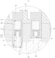
图17为图16的A处的局部放大图。FIG. 17 is a partial enlarged view of part A of FIG. 16 .
附图标记:Reference number:
100-半导体结构; 10-基底;100-semiconductor structure; 10-substrate;
101-有源区; 102-浅沟道隔离区;101-active region; 102-shallow trench isolation region;
103-凹槽; 104-隔离结构;103-groove; 104-isolation structure;
11-位线接触层; 111-位线接触结构;11-bit line contact layer; 111-bit line contact structure;
12-介质层; 13-空隙;12-dielectric layer; 13-void;
14-第一绝缘层; 15-第二绝缘层;14-first insulating layer; 15-second insulating layer;
16-位线; 161-第一导电层;16-bit line; 161-first conductive layer;
1611-侧墙延伸部; 162-第二导电层;1611-Sidewall extension; 162-Second conductive layer;
163-保护层; 17-字线;163-protective layer; 17-word line;
18-存储节点接触结构; 19-接触插塞;18-storage node contact structure; 19-contact plug;
20-隔离墙。20 - The separation wall.
具体实施方式Detailed ways
为了使本申请实施例的上述目的、特征和优点能够更加明显易懂,下面将结合本申请实施例中的附图,对本申请实施例中的技术方案进行清楚、完整地描述。显然,所描述的实施例仅仅是本申请的一部分实施例,而不是全部的实施例。基于本申请中的实施例,本领域普通技术人员在没有作出创造性劳动的前提下所获得的所有其它实施例,均属于本申请保护的范围。In order to make the above objects, features and advantages of the embodiments of the present application more obvious and easy to understand, the technical solutions in the embodiments of the present application will be clearly and completely described below with reference to the accompanying drawings in the embodiments of the present application. Obviously, the described embodiments are only a part of the embodiments of the present application, but not all of the embodiments. Based on the embodiments in this application, all other embodiments obtained by those of ordinary skill in the art without creative work shall fall within the protection scope of this application.
实施例一Example 1
本申请实施例提供的半导体结构的制作方法用于制作半导体结构,该半导体结构包括但不仅限于为DRAM。The method for fabricating a semiconductor structure provided by the embodiments of the present application is used for fabricating a semiconductor structure, and the semiconductor structure includes but is not limited to a DRAM.
图1为本申请实施例提供的半导体结构的制作方法的流程示意图;图2为本申请实施例提供的设置有位线和字线的基底的俯视示意图;图3至图16为本申请实施例提供的半导体结构的形成过程的剖面结构示意图。1 is a schematic flowchart of a method for fabricating a semiconductor structure provided by an embodiment of the present application; FIG. 2 is a schematic top view of a substrate provided with bit lines and word lines provided by an embodiment of the present application; FIGS. 3 to 16 are embodiments of the present application A schematic cross-sectional structure diagram of the formation process of the semiconductor structure is provided.
如图1所示,本申请实施例提供的半导体结构的制作方法,其步骤包括:As shown in FIG. 1 , the method for fabricating a semiconductor structure provided by an embodiment of the present application includes the following steps:
步骤S101:提供基底,基底中设置有多个间隔设置的有源区。Step S101 : providing a substrate in which a plurality of active regions are arranged at intervals.
可以理解的是,基底用于支撑基底上形成的各膜层或者各器件。其中,基底可以为晶体半导体材料制成,例如,硅(Si)基底,基底还可以为锗化硅(SiGe)基底、碳化硅(SiC)基底、绝缘体上硅(silicon-on-insulator,简称SOI)基底等,在本申请实施例中,基底为硅基底。It can be understood that the substrate is used to support each film layer or each device formed on the substrate. The substrate may be made of a crystalline semiconductor material, for example, a silicon (Si) substrate, and the substrate may also be a silicon germanium (SiGe) substrate, a silicon carbide (SiC) substrate, or a silicon-on-insulator (SOI for short) ) substrate, etc. In the embodiments of the present application, the substrate is a silicon substrate.
如图2所示,通过对基底10进行处理,在基底10中形成浅沟道隔离结构(ShallowTrench Isolation,简称为STI),浅沟道隔离结构将基底10隔离形成多个有源区101。其中,有源区101可以在基底10上呈阵列排布。As shown in FIG. 2 , by processing the
另外,浅沟道隔离结构内填充有氧化硅、氮化硅等绝缘材料,在本实施例中,将填充有上述绝缘材料的浅沟道隔离结构定义为浅沟道隔离区102。In addition, the shallow trench isolation structure is filled with insulating materials such as silicon oxide and silicon nitride. In this embodiment, the shallow trench isolation structure filled with the above insulating material is defined as the shallow
基底10中还设有位线接触结构111以及位于位线接触结构111上的位线16,位线16设置有多条,且多条位线16相互平行且间隔设置,例如,多条位线16等间隔设置;位线16通过位线接触结构111与基底10上的有源区101电连接,例如,位线16可以与有源区101中的源极电连接。The
基底10上还设置有多条相互平行且间隔设置的字线17,例如,多条字线17在基底10上等间隔设置,字线17通常埋入在基底10的半导体层内。The
继续参见图2所示,字线17和位线16可以在基底10中垂直交错设置,以基底10的平面形状为矩形为例,字线17可以沿基底10的长度方向(或宽度方向)延伸,位线16可以沿基底10的宽度方向(或长度方向)延伸。Continuing to refer to FIG. 2 , the word lines 17 and the bit lines 16 may be vertically staggered in the
下面,对在基底10上形成多个间隔设置的位线接触结构以及位于位线接触结构上的位线16的过程,进行具体介绍。Next, the process of forming a plurality of bit line contact structures arranged at intervals on the
步骤S102:去除部分基底,以在基底中形成凹槽,凹槽中至少暴露有源区。Step S102 : removing part of the substrate to form a groove in the substrate, and at least the active region is exposed in the groove.
如图3和图4所示,其具体步骤包括,提供具有隔离结构104的基底10,在基底10上形成第一掩膜层,并通过曝光显影等方式图案化第一掩膜层,以图案化的第一掩膜层为掩膜,去除部分基底10,以在基底10中形成凹槽103(如图4所示),凹槽103中至少暴露有源区101。As shown in FIG. 3 and FIG. 4 , the specific steps include: providing a
需要说明的是,隔离结构104如图3中的虚线区域对应的部分,隔离结构104对应的区域可以包括多个有源区101和隔离有源区101的浅沟道隔离区102,例如,在图3中,一个隔离结构104对应的区域包括两个有源区101和三个浅沟道隔离区102。It should be noted that the
其中,第一掩膜层可以是光敏材料,如光刻胶层或者光阻层等,对此,本实施例不做具体限制。The first mask layer may be a photosensitive material, such as a photoresist layer or a photoresist layer, which is not specifically limited in this embodiment.
可以理解的是,凹槽103中可以只暴露有源区101;或者,凹槽103中除了暴露有源区101以外,还可以暴露部分浅沟道隔离区102。It can be understood that, only the
在具有隔离结构104的基底10上形成第一掩膜层之前,如图3所示,在基底10上可以先形成一层第一绝缘层14,其中,第一绝缘层14可通过物理气相沉积(Physical VaporDeposition,简称PVD)工艺或者化学气相沉积(Chemical Vapor Deposition,简称CVD)工艺等方式在基底10上形成,之后,在第一绝缘层14上形成第一掩膜层,图案化第一掩膜层并以图案化后的第一掩膜层为掩膜,刻蚀第一绝缘层14以及部分基底10,在基底10上形成凹槽103(如图4所示)。Before forming the first mask layer on the
可以理解的是,基底10上与凹槽103对应的第一绝缘层14被去除,保留隔离结构104上的第一绝缘层14,在基底10上形成的凹槽103暴露有源区101,这样,通过使凹槽103暴露有源区101,以便后续在基底10上形成的位线接触结构111能够与有源区101电连接。It can be understood that the first insulating
另外,在基底10上形成位线接触结构111之前,通过保留隔离结构104上的第一绝缘层14,第一绝缘层14可以将形成在隔离结构104上的膜层与有源区101绝缘隔离,避免后续形成位线接触结构层以及位线层等膜层时,导电离子向有源区101扩散而导致半导体结构100的电学性能的可靠性差的问题。In addition, before the bit
其中,第一绝缘层14的材料可以包括氮化硅(SiN)、氧化硅等绝缘材料中的一种,对此,本实施例不做具体限制。The material of the first insulating
步骤S103:在凹槽中与有源区对应的区域上形成位线接触结构。Step S103 : forming a bit line contact structure on a region corresponding to the active region in the groove.
继续参见图3所示,位线接触结构111形成的步骤具体包括:在凹槽103和隔离结构104上通过沉积等方式形成位线接触层11,其中,位线接触层11可通过物理气相沉积工艺或者化学气相沉积工艺等方式形成。Continuing to refer to FIG. 3 , the step of forming the bit
其中,位线接触层11的材料包括但不仅限于多晶硅等材料。The material of the bit
如图4所示,在位线接触层11上形成第二掩膜层,并通过曝光显影等方式图案化第二掩膜层,以图案化的第二掩膜层为掩膜,去除部分位线接触层11,保留在凹槽103中与有源区101对应的位线接触层11形成位线接触结构111。As shown in FIG. 4, a second mask layer is formed on the bit
可以理解的是,保留隔离结构104上的位线接触层11指的是按照产品需求保留的具有预设宽度尺寸的位线接触层11,保留在隔离结构104上的位线接触层11并非完全覆盖隔离结构104。It can be understood that the retention of the bit
示例性的,去除部分位线接触层11可以通过干法刻蚀工艺或者湿法刻蚀工艺刻蚀去除,例如,采用氯气等刻蚀气体对位线接触层11进行干法刻蚀;或者,采用硝酸(HNO3)和氢氟(HF)的混合溶液对位线接触层11进行湿法刻蚀。Exemplarily, the removal of part of the bit
在一些可选的实施例中,位线接触结构111的宽度可以为凹槽103的宽度的1/2~1/3。凹槽103的宽度例如是凹槽103的底部宽度,即凹槽103与基底10接触的宽度。由于位线接触结构111仅与有源区101接触,如果位线接触结构111的宽度与凹槽103底部宽度的比值大于1/2,则不利于后续形成空隙;如果位线接触结构111的宽度与凹槽103的宽度的比值小于1/3,则导致位线接触结构111的宽度较窄,有源区101与位线接触结构111之间的接触电阻会变大,同时还不利于位线接触结构111承载后续的位线。In some optional embodiments, the width of the bit
另外,位线接触结构111的截面的对称中心轴线与凹槽103的截面的对称中心轴线重合。例如,当凹槽103为圆形、正方形等规则形状的凹槽103时,位线接触结构111的对称中心轴线与凹槽103的对称中心轴线重合。In addition, the central axis of symmetry of the cross-section of the bit
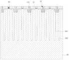
在凹槽103中与有源区101对应的区域上形成位线接触结构111之后,如图5所示,在形成的位线接触结构111、凹槽103以及隔离结构104上形成第二绝缘层15。其中,第二绝缘层15可以是氮化硅。After the bit
步骤S104:在凹槽和隔离结构上形成有介质层,介质层与位线接触结构的侧壁之间形成有顶部开口的空隙。Step S104 : a dielectric layer is formed on the groove and the isolation structure, and a gap with a top opening is formed between the dielectric layer and the sidewall of the bit line contact structure.
如图6所示,其具体形成过程为:在第二绝缘层15上通过物理气相沉积工艺或者化学气相沉积工艺形成介质层12。其中,介质层12包括但不仅限于氧化硅。As shown in FIG. 6 , the specific formation process is as follows: the
可以理解的是,在凹槽103和隔离结构104上形成的介质层12的高度高于位线接触结构111的高度。It can be understood that the height of the
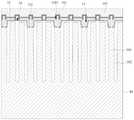
如图7所示,可通过化学机械抛光(Chemical Mechanical Polishing,简称CMP)或者刻蚀等工艺去除部分介质层12,在去除部分介质层12的同时,将位线接触结构111上的绝缘层一并去除,以使介质层12与位线接触结构111的顶部平齐,以暴露位线接触结构111;或者,也可以去除部分位线接触结构111,降低位线接触结构111的高度,这样,可以降低后续在位线接触结构111上形成的位线的高度。As shown in FIG. 7 , part of the
如图8所示,当位线接触结构111暴露后,可通过湿法刻蚀工艺继续刻蚀介质层12,以使位线接触结构111的顶部高于介质层12的顶部。例如,湿法刻蚀工艺可以包括但不仅限于采用氢氟酸刻蚀溶液刻蚀介质层12。As shown in FIG. 8 , after the bit
在另一种可选的实施例中,也可通过化学机械抛光等方式去除部分介质层12,以使介质层12与第二绝缘层15的顶部平齐,之后,刻蚀去除第二绝缘层15的同时,将位线接触结构111顶部的绝缘层一并去除。In another optional embodiment, part of the
在一些可选的实施方式中,位线接触结构111的顶部与介质层12的顶部的高度差为位线接触结构111的高度的1/10~9/10。In some optional embodiments, the height difference between the top of the bit
示例性的,位线接触结构111的顶部与介质层12的顶部的高度差为位线接触结构111的高度的1/10、1/5、1/2、9/10等,对此,本实施例不做具体限制。本实施例通过移除部分介质层12使得第二绝缘层15暴露出来,从而有利于后续刻蚀该第二绝缘层15。位线接触结构111的顶部与介质层12的顶部的高度差越大,在位线接触结构111形成的空隙的高度越大,因此有利于减小位线接触结构111与存储节点接触结构之间产生的寄生电容以及漏电现象,从而提高半导体结构100的性能的可靠性。Exemplarily, the height difference between the top of the bit
如图9所示,可采用湿法刻蚀工艺或干法刻蚀工艺去除位线接触结构111侧壁的第二绝缘层15,保留位线接触结构111侧壁的底部的预设高度的第二绝缘层15,以使介质层12与各位线接触结构111的侧壁之间形成有顶部开口的空隙13。As shown in FIG. 9 , a wet etching process or a dry etching process may be used to remove the second insulating
示例性的,湿法刻蚀可采用磷酸等刻蚀溶液去除位线接触结构111侧壁的第二绝缘层15。Exemplarily, the wet etching may use an etching solution such as phosphoric acid to remove the second insulating
可以理解的是,通过在介质层12与各位线接触结构111的侧壁之间设置空隙13,由于空气的介电常数低于其他任何材质的介电常数,因此,在本申请中,通过使介质层12与各位线接触结构111的侧壁之间形成空隙13,以通过空隙13隔离位线接触结构111与存储节点接触结构,从而减小位线接触结构111与存储节点接触结构之间产生的寄生电容以及漏电现象,从而提高半导体结构100的性能的可靠性。It can be understood that by arranging
在一些可选的实施例中,空隙13的宽度与位线接触结构111的宽度的比值为1:2~1:1。In some optional embodiments, the ratio of the width of the void 13 to the width of the bit
可以理解的是在,在保证位线接触结构111具有足够的工作可靠性的同时,空隙13的宽度越大越好,以减小位线接触结构111与后续形成的存储节点接触结构之间产生的寄生电容,从而提高半导体结构100的性能的可靠性。It can be understood that while ensuring the bit
步骤S105:在位线接触结构上形成位线,封堵空隙的开口。Step S105 : forming a bit line on the bit line contact structure to block the opening of the gap.
作为一种可选的实施方式,如图10至图13所示,位线16在位线接触结构111的侧壁上形成有向空隙13内延伸的侧墙延伸部1611,侧墙延伸部1611封堵空隙13的开口。As an optional implementation manner, as shown in FIG. 10 to FIG. 13 , on the sidewall of the bit
可以理解的是,位线16通过设置侧墙延伸部1611,使侧墙延伸部1611向空隙13内延伸以封堵空隙13的开口,这样,位线16可以包裹部分位线接触结构111的侧壁,由此增加了位线16与位线接触结构111的接触面积,可以有效的减小位线16与位线接触结构111之间的接触电阻,以保证位线16的导电性能。It can be understood that the
沿基底10的竖直方向,侧墙延伸部1611向空隙13内的延伸深度为空隙13的深度的1/2~1/3。这样,一方面,通过在位线接触结构111的侧壁与介质层12之间形成足够空间的空隙13,以减小位线接触结构111与存储节点接触结构等之间生成的寄生电容,以提高半导体结构100的性能可靠性;另一方面,通过侧墙延伸部1611沿空隙13内延伸,以使位线16包裹位线接触结构111的部分侧壁,以减小位线16与位线接触结构111之间的接触电阻,从而提高位线16的导电性能。Along the vertical direction of the
位线16包括形成在位线接触结构111上的第一导电层161、形成在第一导电层161上的第二导电层162以及形成在第二导电层162上的保护层163;第一导电层161在位线接触结构111的侧壁上形成侧墙延伸部1611。The
具体的形成过程包括:如图10所示,在介质层12和位线接触结构111上形成第一导电层161,且部分第一导电层161封堵空隙13的开口并向空隙13内延伸,延伸至空隙13内的第一导电层161形成侧墙延伸部1611,这样,第一导电层161包裹部分位线接触结构111的侧壁,增加了第一导电层161与位线接触结构111的接触面积,可以减小第一导电层161与位线接触结构111之间的接触电阻,从而增大位线16的导电性能。其中,第一导电层161的材料包括但不仅限于氮化钛等导电材质。The specific forming process includes: as shown in FIG. 10 , forming a first
如图11所示,在第一导电层161上通过物理气相沉积工艺或者化学气相沉积工艺形成第二导电层162,其中,第二导电层162的材料包括但不仅限于金属钨等导电材质。As shown in FIG. 11 , the second
如图12所示,在第二导电层162上形成掩膜层,并图案化掩膜层,以使图案化的掩膜层暴露介质层12上的第二导电层162,并通过干法刻蚀工艺或者湿法刻蚀工艺去除介质层12上的第一导电层161和第二导电层162,以暴露介质层12,保留位线接触结构111上的第一导电层161和第二导电层162,以及保留空隙13的开口处的第一导电层161和保留开口处对应的第一导电层161上的第二导电层162。As shown in FIG. 12 , a mask layer is formed on the second
如图13所示,在介质层12以及第二导电层162上形成保护层163,各位线接触结构111上的第一导电层161、第二导电层162以及保护层163形成位线16。As shown in FIG. 13 , a
可以理解的是,保护层163可以为绝缘材料,保护层163的材料包括但不仅限于氮化硅等绝缘材质。It can be understood that the
可以理解的是,保护层163可以防止位线16与存储节点接触结构之间的电连接。It is understood that the
如图14至图17所示,在形成多个间隔设置的位线16之后,接着可以在基底10上依次形成多个间隔设置的接触插塞19(如图15所示)和多个间隔设置的存储节点接触结构18(如图16所示),各存储节点接触结构18与各接触插塞19一一对应,且各存储节点接触结构18形成在各接触插塞19上。As shown in FIGS. 14 to 17 , after a plurality of spaced
具体的,各接触插塞19位于相邻位线16之间,且各接触插塞19与各有源区101对应且电连接。形成各接触插塞19后,在基底10上形成各存储节点接触结构18,各存储节点接触结构18形成在各接触插塞19上。在实际应用中,电容器与存储节点接触结构18电连接,通过存储节点接触结构18和接触插塞19实现电容器与有源区101电连接。Specifically, each
示例性的,构成接触插塞19的材料可以包括多晶硅等导电材料,构成存储节点接触结构18的材料可以包括钨等导电材料。Exemplarily, the material constituting the
具体形成各接触插塞19和各存储节点接触结构18时,例如,可以先在基底10上沉积一层多晶硅层,然后,通过光刻工艺对该多晶硅层进行刻蚀,从而,将该多晶硅层图形化,形成多个间隔设置的各接触插塞19,各接触插塞19对应位于相邻的位线16之间。When forming each
类似的,在形成各接触插塞19后,可以在基底10上沉积一层钨层,该钨层覆盖各接触插塞19,然后,通过光刻工艺对该钨层进行刻蚀,从而,将该钨层图形化,形成多个间隔设置的存储节点接触结构18,各存储节点接触结构18对应连接在各接触插塞19的顶表面上。Similarly, after each
另外,为了将接触插塞19与位线16之间绝缘隔离,避免位线16和电容器短接,保证位线16和电容器的工作性能,并且,避免在形成接触插塞19的过程中,位线16和接触插塞19之间的离子相互扩散,避免对位线16和接触插塞19的性能造成影响,本实施例中,位线16和接触插塞19之间还设置有隔离墙20,如图14。In addition, in order to isolate the contact plug 19 from the
对此,在形成接触插塞19之前,可以先在基底10上和位线16上形成隔离墙20,各隔离墙20包裹在各位线16的侧壁面和顶面上。这样,形成包裹各位线16的侧壁面和顶面的隔离墙20后,再在基底10上形成各接触插塞19,接触插塞19和位线16之间通过隔离墙20绝缘隔离。示例性的,构成隔离墙20的材料可以包括氮化硅、氧化硅等。In this regard, before forming the contact plugs 19 ,
如图16所示,隔离墙20和接触插塞19形成后,然后沉积导电层,例如,导电层为钨层,导电层覆盖隔离墙20和接触插塞19,采用光刻工艺对导电层进行刻蚀,将导电层图形化,形成存储节点接触结构18。As shown in FIG. 16 , after the
在实际应用中,电容器和接触插塞19之间往往存在一定的偏移度,无法做到电容器和接触插塞19完全对应,因此,本实施例中,存储节点接触结构18可以相对接触插塞19具有一定的偏移,以使存储节点接触结构18更好的与电容器对应,增大存储节点接触结构18与电容器之间的接触面积,保证电容器与存储节点接触结构18接触良好。In practical applications, there is often a certain degree of offset between the capacitor and the
为了使存储节点接触结构18对应电容器的一侧相对接触插塞19偏移一定距离,在沉积完成对应存储节点接触结构18的导电层后,例如,沉积完成钨层后,在对钨层进行刻蚀时,刻蚀所用的掩膜版上的掩膜图形与接触插塞19之间可以具有一定的偏移。如此,如图16和图17所示,使存储节点接触结构18的下半部分填充在各隔离墙20之间,存储节点接触结构18的上半部分的边缘可以搭接在隔离墙20的顶表面的部分区域,而隔离墙20的顶表面的另一部分区域暴露,以绝缘隔离相邻的存储节点接触结构18。In order to offset the side of the storage
另外,在形成接触插塞19之后,形成存储节点接触结构18之前,可以在接触插塞19上先形成一层阻挡层(图中未示出),即,形成接触插塞19和隔离墙20后,依次沉积形成阻挡层和导电层,然后对导电层和阻挡层进行刻蚀,形成存储节点接触结构18,并将阻挡层图形化,暴露出隔离墙20的部分区域。In addition, after the contact plugs 19 are formed and before the storage
通过在接触插塞19和存储节点接触结构18之间设置阻挡层,阻挡层可阻挡存储节点接触结构18和接触插塞19之间的材料相互渗透,阻挡层还可以实现接触插塞19和导电层之间的电连接。示例性的,构成阻挡层的材料可以为氮化钛。By arranging a barrier layer between the
另外,为了减小位线接触结构111与存储节点接触结构18之间的寄生电容,在本申请实施例中,通过在位线接触结构111的侧壁形成空隙13,从而减小位线接触结构111与存储节点接触结构18之间生成的寄生电容,也可以减小位线16与存储节点接触结构18之间的漏电现象,避免半导体结构100的可靠性低的技术问题,从而提高半导体结构100的工作可靠性。In addition, in order to reduce the parasitic capacitance between the bit
实施例二Embodiment 2
本申请实施例提供的半导体结构100,采用实施例一中的半导体结构100的制作方法制作而成。The
参照图2至图17所示,半导体结构100包括基底10,基底10上形成有浅沟道隔离结构,浅沟道隔离结构隔离出多个区域,该多个区域形成基底10上多个间隔设置的有源区101(如图2所示)。基底10上还设有凹槽103以及隔离凹槽103的隔离结构104(如图4所示),凹槽103中至少暴露有源区101,在凹槽103上设置有位线接触结构111,可以理解的是,凹槽103中的位线接触结构111与凹槽103中的有源区101一一对应并接触,以使位于凹槽103中的位线接触结构111与凹槽103中的有源区101电连接。Referring to FIGS. 2 to 17 , the
参见图16和图17所示,凹槽103、位线接触结构111以及隔离结构104上设有介质层12,介质层12与位线接触结构111的侧壁之间形成有顶部开口的空隙13;基底10上还形成有多个位线16,各位线16一一对应设置在各位线接触结构111,以使位线16通过位线接触结构111与有源区101电连接,而各部分位线16封堵空隙13的开口,这样,通过在介质层12与位线接触结构的侧壁之间形成空隙13,该空隙13可以减小位线接触结构111与半导体结构100中存储节点接触结构18等之间生成的寄生电容,从而提高半导体结构100的工作可靠性。Referring to FIG. 16 and FIG. 17 , a
本申请实施例提供的半导体结构,通过在介质层与位线接触结构的侧壁之间形成有顶部开口的空隙,在位线接触结构上形成位线,位线封堵空隙的开口,由于空气的介电常数较小,因此,通过在介质层与位线接触结构的侧壁之间形成空隙,以减小位线接触结构与存储节点接触之间生成的寄生电容,从而提高半导体结构的工作可靠性。In the semiconductor structure provided by the embodiments of the present application, by forming a gap with a top opening between the dielectric layer and the sidewall of the bit line contact structure, a bit line is formed on the bit line contact structure, and the bit line blocks the opening of the gap, and due to the air Therefore, by forming a gap between the dielectric layer and the sidewall of the bit line contact structure, the parasitic capacitance generated between the bit line contact structure and the storage node contact is reduced, thereby improving the work of the semiconductor structure reliability.
本说明书中各实施例或实施方式采用递进的方式描述,每个实施例重点说明的都是与其他实施例的不同之处,各个实施例之间相同相似部分相互参见即可。The embodiments or implementations in this specification are described in a progressive manner, and each embodiment focuses on the differences from other embodiments, and the same and similar parts between the various embodiments may be referred to each other.
在本说明书的描述中,参考术语“一个实施方式”、“一些实施方式”、“示意性实施方式”、“示例”、“具体示例”、或“一些示例”等的描述意指结合实施方式或示例描述的具体特征、结构、材料或者特点包含于本申请的至少一个实施方式或示例中。在本说明书中,对上述术语的示意性表述不一定指的是相同的实施方式或示例。而且,描述的具体特征、结构、材料或者特点可以在任何的一个或多个实施方式或示例中以合适的方式结合。In the description of this specification, reference to the terms "one embodiment," "some embodiments," "exemplary embodiment," "example," "specific example," or "some examples," or the like, is meant to incorporate embodiments. A particular feature, structure, material, or characteristic described or exemplified is included in at least one embodiment or example of the present application. In this specification, schematic representations of the above terms do not necessarily refer to the same embodiment or example. Furthermore, the particular features, structures, materials or characteristics described may be combined in any suitable manner in any one or more embodiments or examples.
最后应说明的是:以上各实施例仅用以说明本申请的技术方案,而非对其限制;尽管参照前述各实施例对本申请进行了详细的说明,本领域的普通技术人员应当理解:其依然可以对前述各实施例所记载的技术方案进行修改,或者对其中部分或者全部技术特征进行等同替换;而这些修改或者替换,并不使相应技术方案的本质脱离本申请各实施例技术方案的范围。Finally, it should be noted that the above embodiments are only used to illustrate the technical solutions of the present application, but not to limit them; although the present application has been described in detail with reference to the foregoing embodiments, those of ordinary skill in the art should understand that: The technical solutions described in the foregoing embodiments can still be modified, or some or all of the technical features thereof can be equivalently replaced; and these modifications or replacements do not make the essence of the corresponding technical solutions deviate from the technical solutions of the embodiments of the present application. scope.
Claims (19)
Translated fromChinesePriority Applications (1)
| Application Number | Priority Date | Filing Date | Title |
|---|---|---|---|
| CN202210201828.8ACN114649270A (en) | 2022-03-02 | 2022-03-02 | Semiconductor structure and manufacturing method thereof |
Applications Claiming Priority (1)
| Application Number | Priority Date | Filing Date | Title |
|---|---|---|---|
| CN202210201828.8ACN114649270A (en) | 2022-03-02 | 2022-03-02 | Semiconductor structure and manufacturing method thereof |
Publications (1)
| Publication Number | Publication Date |
|---|---|
| CN114649270Atrue CN114649270A (en) | 2022-06-21 |
Family
ID=81993438
Family Applications (1)
| Application Number | Title | Priority Date | Filing Date |
|---|---|---|---|
| CN202210201828.8APendingCN114649270A (en) | 2022-03-02 | 2022-03-02 | Semiconductor structure and manufacturing method thereof |
Country Status (1)
| Country | Link |
|---|---|
| CN (1) | CN114649270A (en) |
Cited By (4)
| Publication number | Priority date | Publication date | Assignee | Title |
|---|---|---|---|---|
| CN115942744A (en)* | 2023-02-15 | 2023-04-07 | 长鑫存储技术有限公司 | Manufacturing method of semiconductor structure and semiconductor structure |
| CN116171043A (en)* | 2023-04-24 | 2023-05-26 | 长鑫存储技术有限公司 | Semiconductor structure and preparation method thereof |
| WO2024109156A1 (en)* | 2022-11-22 | 2024-05-30 | 长鑫存储技术有限公司 | Semiconductor structure and forming method therefor |
| CN119031700A (en)* | 2023-05-19 | 2024-11-26 | 长鑫存储技术有限公司 | Semiconductor structure and method for manufacturing the same |
- 2022
- 2022-03-02CNCN202210201828.8Apatent/CN114649270A/enactivePending
Cited By (5)
| Publication number | Priority date | Publication date | Assignee | Title |
|---|---|---|---|---|
| WO2024109156A1 (en)* | 2022-11-22 | 2024-05-30 | 长鑫存储技术有限公司 | Semiconductor structure and forming method therefor |
| CN115942744A (en)* | 2023-02-15 | 2023-04-07 | 长鑫存储技术有限公司 | Manufacturing method of semiconductor structure and semiconductor structure |
| CN115942744B (en)* | 2023-02-15 | 2023-08-04 | 长鑫存储技术有限公司 | Method for manufacturing semiconductor structure and semiconductor structure |
| CN116171043A (en)* | 2023-04-24 | 2023-05-26 | 长鑫存储技术有限公司 | Semiconductor structure and preparation method thereof |
| CN119031700A (en)* | 2023-05-19 | 2024-11-26 | 长鑫存储技术有限公司 | Semiconductor structure and method for manufacturing the same |
Similar Documents
| Publication | Publication Date | Title |
|---|---|---|
| CN110581103B (en) | Semiconductor element and manufacturing method thereof | |
| JP3589791B2 (en) | DRAM cell manufacturing method | |
| CN100561728C (en) | Semiconductor device and manufacturing method thereof | |
| CN110061001B (en) | Semiconductor element and manufacturing method thereof | |
| CN114649270A (en) | Semiconductor structure and manufacturing method thereof | |
| CN109037217B (en) | memory device | |
| CN1317769C (en) | Semiconductor storage device and its producing method | |
| CN115666132B (en) | Semiconductor structure preparation method and semiconductor structure | |
| CN103390621B (en) | Preparation method of storage device | |
| CN116113231B (en) | Semiconductor structure and manufacturing method thereof | |
| CN114530419A (en) | Memory forming method and memory | |
| WO2022088758A1 (en) | Method for forming semiconductor structure, and semiconductor structure | |
| CN1225027C (en) | 6 1/4 ff DRAM unit structure with arrangement of four node tied by per bit line and two-stage word line | |
| CN114420641A (en) | Method for forming semiconductor structure and semiconductor structure | |
| JP3229279B2 (en) | Method of forming trench buried strap | |
| CN113053897B (en) | Memory and method of making the same | |
| WO2023060796A1 (en) | Semiconductor structure and manufacturing method therefor | |
| CN115148663A (en) | Semiconductor structure and method of making the same | |
| TWI843223B (en) | Decoupling capacitor structure and semiconductor device including the same | |
| US5665626A (en) | Method of making a chimney capacitor | |
| CN112466888A (en) | Method for filling polycrystalline silicon material in semiconductor device structure and preparing 3D NAND memory | |
| TW202329398A (en) | Semiconductor structure and manufacturing method thereof | |
| CN100373623C (en) | Dynamic random access memory cell and array thereof, and manufacturing method of the array | |
| US11856756B2 (en) | Semiconductor structure and manufacturing method thereof | |
| CN115172267A (en) | Semiconductor structure and preparation method thereof |
Legal Events
| Date | Code | Title | Description |
|---|---|---|---|
| PB01 | Publication | ||
| PB01 | Publication | ||
| SE01 | Entry into force of request for substantive examination | ||
| SE01 | Entry into force of request for substantive examination |