CN114647340A - Integrated touch screen - Google Patents
Integrated touch screenDownload PDFInfo
- Publication number
- CN114647340A CN114647340ACN202210303900.8ACN202210303900ACN114647340ACN 114647340 ACN114647340 ACN 114647340ACN 202210303900 ACN202210303900 ACN 202210303900ACN 114647340 ACN114647340 ACN 114647340A
- Authority
- CN
- China
- Prior art keywords
- display
- touch
- display pixels
- pixels
- circuit elements
- Prior art date
- Legal status (The legal status is an assumption and is not a legal conclusion. Google has not performed a legal analysis and makes no representation as to the accuracy of the status listed.)
- Pending
Links
Images


Classifications
- G—PHYSICS
- G06—COMPUTING OR CALCULATING; COUNTING
- G06F—ELECTRIC DIGITAL DATA PROCESSING
- G06F3/00—Input arrangements for transferring data to be processed into a form capable of being handled by the computer; Output arrangements for transferring data from processing unit to output unit, e.g. interface arrangements
- G06F3/01—Input arrangements or combined input and output arrangements for interaction between user and computer
- G06F3/03—Arrangements for converting the position or the displacement of a member into a coded form
- G06F3/041—Digitisers, e.g. for touch screens or touch pads, characterised by the transducing means
- G06F3/0412—Digitisers structurally integrated in a display
- G—PHYSICS
- G06—COMPUTING OR CALCULATING; COUNTING
- G06F—ELECTRIC DIGITAL DATA PROCESSING
- G06F3/00—Input arrangements for transferring data to be processed into a form capable of being handled by the computer; Output arrangements for transferring data from processing unit to output unit, e.g. interface arrangements
- G06F3/01—Input arrangements or combined input and output arrangements for interaction between user and computer
- G06F3/03—Arrangements for converting the position or the displacement of a member into a coded form
- G06F3/041—Digitisers, e.g. for touch screens or touch pads, characterised by the transducing means
- G06F3/0416—Control or interface arrangements specially adapted for digitisers
- G06F3/04164—Connections between sensors and controllers, e.g. routing lines between electrodes and connection pads
- G—PHYSICS
- G06—COMPUTING OR CALCULATING; COUNTING
- G06F—ELECTRIC DIGITAL DATA PROCESSING
- G06F3/00—Input arrangements for transferring data to be processed into a form capable of being handled by the computer; Output arrangements for transferring data from processing unit to output unit, e.g. interface arrangements
- G06F3/01—Input arrangements or combined input and output arrangements for interaction between user and computer
- G06F3/03—Arrangements for converting the position or the displacement of a member into a coded form
- G06F3/041—Digitisers, e.g. for touch screens or touch pads, characterised by the transducing means
- G06F3/044—Digitisers, e.g. for touch screens or touch pads, characterised by the transducing means by capacitive means
- G06F3/0443—Digitisers, e.g. for touch screens or touch pads, characterised by the transducing means by capacitive means using a single layer of sensing electrodes
- G—PHYSICS
- G06—COMPUTING OR CALCULATING; COUNTING
- G06F—ELECTRIC DIGITAL DATA PROCESSING
- G06F3/00—Input arrangements for transferring data to be processed into a form capable of being handled by the computer; Output arrangements for transferring data from processing unit to output unit, e.g. interface arrangements
- G06F3/01—Input arrangements or combined input and output arrangements for interaction between user and computer
- G06F3/03—Arrangements for converting the position or the displacement of a member into a coded form
- G06F3/041—Digitisers, e.g. for touch screens or touch pads, characterised by the transducing means
- G06F3/044—Digitisers, e.g. for touch screens or touch pads, characterised by the transducing means by capacitive means
- G06F3/0445—Digitisers, e.g. for touch screens or touch pads, characterised by the transducing means by capacitive means using two or more layers of sensing electrodes, e.g. using two layers of electrodes separated by a dielectric layer
- G—PHYSICS
- G09—EDUCATION; CRYPTOGRAPHY; DISPLAY; ADVERTISING; SEALS
- G09G—ARRANGEMENTS OR CIRCUITS FOR CONTROL OF INDICATING DEVICES USING STATIC MEANS TO PRESENT VARIABLE INFORMATION
- G09G3/00—Control arrangements or circuits, of interest only in connection with visual indicators other than cathode-ray tubes
- G09G3/20—Control arrangements or circuits, of interest only in connection with visual indicators other than cathode-ray tubes for presentation of an assembly of a number of characters, e.g. a page, by composing the assembly by combination of individual elements arranged in a matrix no fixed position being assigned to or needed to be assigned to the individual characters or partial characters
- G—PHYSICS
- G06—COMPUTING OR CALCULATING; COUNTING
- G06F—ELECTRIC DIGITAL DATA PROCESSING
- G06F2203/00—Indexing scheme relating to G06F3/00 - G06F3/048
- G06F2203/041—Indexing scheme relating to G06F3/041 - G06F3/045
- G06F2203/04111—Cross over in capacitive digitiser, i.e. details of structures for connecting electrodes of the sensing pattern where the connections cross each other, e.g. bridge structures comprising an insulating layer, or vias through substrate
Landscapes
- Engineering & Computer Science (AREA)
- Theoretical Computer Science (AREA)
- General Engineering & Computer Science (AREA)
- Physics & Mathematics (AREA)
- General Physics & Mathematics (AREA)
- Human Computer Interaction (AREA)
- Computer Networks & Wireless Communication (AREA)
- Computer Hardware Design (AREA)
- Liquid Crystal (AREA)
- Devices For Indicating Variable Information By Combining Individual Elements (AREA)
- Position Input By Displaying (AREA)
- Control Of Indicators Other Than Cathode Ray Tubes (AREA)
Abstract
Description
Translated fromChinese本申请是申请日为2010年2月2日申请号为201080010343.6(国际申请号:PCT/US2010/022888)发明名称为“集成触摸屏”的发明专利申请的分案申请,本申请直接针对的分案申请的申请号为201910050920.7、发明名称为“集成触摸屏”。This application is a divisional application for an invention patent application whose application date is February 2, 2010 and the application number is 201080010343.6 (International Application No.: PCT/US2010/022888). The application number of the application is 201910050920.7, and the name of the invention is "integrated touch screen".
技术领域technical field
本发明一般涉及包括显示像素叠层的显示器,且更具体而言涉及集成到显示器的显示像素叠层的触摸感应电路。The present invention relates generally to displays including display pixel stacks, and more particularly to touch sensing circuits integrated into display pixel stacks of displays.
背景技术Background technique
很多类型的输入设备当前可用于在计算系统中执行操作,诸如按钮或键、鼠标、跟踪球、操纵杆、触摸传感器面板、触摸屏等。尤其是,因为其操作简单和多功能性以及其不断下降的价格,触摸屏正变得越来越流行。触摸屏可以包括:触摸传感器面板,其可以是具有触摸敏感表面的透晰面板,以及诸如液晶显示器(LCD)的显示设备,其可以部分或完全布置在该面板后面,使得触摸敏感表面可以覆盖显示设备的可观看区域的至少一部分。触摸屏可以允许用户通过通常在显示设备显示的用户界面(UI)所指示的位置处使用手指、铁笔或其他对象触摸该触摸传感器面板而执行各种功能。一般而言,触摸屏可以识别触摸传感器面板上的触摸和触摸的位置,且计算系统然后可根据触摸时出现的显示来解读该触摸,且此后可以基于该触摸执行一个或多个动作。在一些触摸感应系统的情况下,不需要显示器上的物理触摸来检测触摸。例如,在一些电容型触摸感应系统中,用于检测触摸的边缘场可以延伸出显示器的表面,且接近该表面的对象可以被检测到在表面附近而无需实际触摸该表面。Many types of input devices are currently available for performing operations in computing systems, such as buttons or keys, mice, trackballs, joysticks, touch sensor panels, touch screens, and the like. In particular, touch screens are becoming more and more popular because of their simplicity of operation and versatility, as well as their falling prices. The touch screen may include a touch sensor panel, which may be a clear panel with a touch-sensitive surface, and a display device, such as a liquid crystal display (LCD), which may be partially or fully disposed behind the panel such that the touch-sensitive surface may cover the display device at least part of the viewable area. A touch screen may allow a user to perform various functions by touching the touch sensor panel with a finger, stylus, or other object, typically at a location indicated by a user interface (UI) displayed by the display device. In general, a touch screen can identify a touch on a touch sensor panel and the location of the touch, and a computing system can then interpret the touch from the display that occurs when the touch is made, and can thereafter perform one or more actions based on the touch. In the case of some touch-sensing systems, no physical touch on the display is required to detect a touch. For example, in some capacitive touch-sensing systems, the fringing field used to detect touch can extend beyond the surface of the display, and objects approaching the surface can be detected near the surface without actually touching the surface.
电容触摸传感器面板可以由通常在基本透明的基板上在水平和垂直方向以行和列布置的诸如氧化铟锡(ITO)的基本透明的导电材料的驱动和感应线的矩阵形成。如上所述,部分地由于其基本透明性,电容触摸传感器面板可以覆盖在显示器上以形成触摸屏。然而,使用触摸传感器面板覆盖显示器可具有诸如增加的重量和厚度、驱动触摸传感器面板所需的附加功率以及显示器的降低的亮度的缺点。Capacitive touch sensor panels may be formed from a matrix of drive and sense lines of a substantially transparent conductive material, such as indium tin oxide (ITO), typically arranged in rows and columns in horizontal and vertical directions on a substantially transparent substrate. As mentioned above, capacitive touch sensor panels can be overlaid on a display to form a touch screen, in part due to their substantial transparency. However, using a touch sensor panel to cover a display can have disadvantages such as increased weight and thickness, additional power required to drive the touch sensor panel, and reduced brightness of the display.
发明内容SUMMARY OF THE INVENTION
本发明涉及集成到显示器(诸如LCD显示器)的显示像素叠层(即,形成显示像素的堆叠材料层)的触摸感应电路。显示像素叠层中的电路元件可以被分组在一起以形成感应显示器上或显示器附近的触摸的触摸感应电路。该触摸感应电路例如可以包括诸如驱动线和感应线的触摸信号线、接地区域和其他电路。集成触摸屏可以包括多功能电路元件,该多功能电路元件可以形成被设计成操作为显示系统的电路的显示电路的一部分,以在显示器上产生图像,且还可以形成感应显示器上或显示器附近的一个或多个触摸的触摸感应系统的触摸感应电路的一部分。该多功能电路元件例如可以是LCD的显示像素中的电容,其可以被配置成操作为显示系统中显示电路的存储电容/电极、公共电极、导电引线/路径等,且还可以被配置成操作为触摸感应电路的电路元件。以这种方式,例如,在一些实施例中,可以使用较少的部件和/或处理步骤制造具有集成触摸感应功能的显示器,且该显示器本身可以更薄、更亮且需要更少的功率。The present invention relates to touch-sensing circuits integrated into display pixel stacks (ie, stacked layers of material forming display pixels) of a display, such as an LCD display. Circuit elements in a display pixel stack can be grouped together to form touch-sensing circuits that sense touch on or near the display. The touch sensing circuit may include, for example, touch signal lines such as drive and sense lines, ground regions, and other circuits. The integrated touch screen can include multifunctional circuit elements that can form part of a display circuit designed to operate as a circuit of a display system to produce an image on the display, and can also form a sensor on or near the display. A portion of the touch-sensing circuitry of a touch-sensing system of one or more touches. The multifunctional circuit element may be, for example, a capacitor in a display pixel of an LCD, which may be configured to operate as a storage capacitor/electrode, common electrode, conductive lead/path, etc. of a display circuit in a display system, and may also be configured to operate Circuit components for touch sensing circuits. In this way, for example, in some embodiments, fewer components and/or processing steps may be used to manufacture displays with integrated touch-sensing functionality, and the displays themselves may be thinner, brighter, and require less power.
附图说明Description of drawings
图1A-图1C说明示例移动电话、示例数字媒体播放器以及示例个人计算机,它们均包括根据本公开的实施例的示例集成触摸屏。1A-1C illustrate an example mobile phone, an example digital media player, and an example personal computer, each including an example integrated touch screen in accordance with embodiments of the present disclosure.
图1D-图1G说明包括根据本公开的实施例的触摸屏的示例集成触摸屏系统。1D-1G illustrate an example integrated touchscreen system including a touchscreen according to embodiments of the present disclosure.
图2是说明根据本公开的实施例的示例集成触摸屏的一个实施方式的示例计算系统的框图。2 is a block diagram of an example computing system illustrating one implementation of an example integrated touch screen according to an embodiment of the present disclosure.
图3是图2的触摸屏的更详细的视图,示出根据本公开的实施例的驱动线和感应线的示例配置。3 is a more detailed view of the touch screen of FIG. 2, showing an example configuration of drive lines and sense lines according to embodiments of the present disclosure.
图4说明根据本公开的实施例的示例配置,其中触摸感应电路包括公共电极(Vcom)。4 illustrates an example configuration in which the touch sensing circuit includes a common electrode (Vcom) in accordance with an embodiment of the present disclosure.
图5说明根据本公开的实施例的导线的示例配置。5 illustrates an example configuration of wires in accordance with embodiments of the present disclosure.
图6-图8是说明示出根据本公开的实施例的示例显示像素的更多细节的平面图和侧视图。6-8 are plan and side views illustrating further details showing example display pixels according to embodiments of the present disclosure.
图9是根据本公开的实施例包括多个子像素的示例触摸屏的部分电路图。9 is a partial circuit diagram of an example touch screen including a plurality of sub-pixels according to an embodiment of the present disclosure.
图10-图12B说明根据本公开的示例触摸感应操作。10-12B illustrate example touch sensing operations in accordance with the present disclosure.
图13A-图13B示出根据本公开的实施例在触摸屏的触摸阶段中被分组到用作触摸感应电路的区域中的多功能显示像素的另一示例配置。13A-13B illustrate another example configuration of multi-function display pixels grouped into areas serving as touch-sensing circuits during the touch phase of a touch screen in accordance with embodiments of the present disclosure.
图14A-图16C说明根据本公开的实施例的显示像素的多功能电路元件的另一示例配置。14A-16C illustrate another example configuration of a multifunction circuit element of a display pixel according to an embodiment of the present disclosure.
图17-图20说明根据本公开的实施例的不同制造阶段中的示例显示像素。17-20 illustrate example display pixels in various stages of fabrication in accordance with embodiments of the present disclosure.
图21A说明用于根据本公开的实施例的一个示例触摸像素的显示像素的示例布局。21A illustrates an example layout of a display pixel for one example touch pixel according to an embodiment of the present disclosure.
图21B是图21A的一部分的放大图,说明根据本公开的实施例的示例驱动隧道。21B is an enlarged view of a portion of FIG. 21A illustrating an example drive tunnel according to an embodiment of the present disclosure.
图21C说明根据本公开的实施例的示例驱动隧道连接。21C illustrates an example driven tunnel connection according to an embodiment of the present disclosure.
图21D说明根据本公开的实施例的另一示例驱动隧道连接。21D illustrates another example driven tunnel connection according to embodiments of the present disclosure.
图22-1和22-2说明可以包括诸如图21A中示出的示例触摸像素的示例触摸像素布局。22-1 and 22-2 illustrate example touch pixel layouts that may include example touch pixels such as shown in FIG. 21A.
图23是根据本公开的实施例包括高阻(R)屏蔽的示例触摸屏的侧视图。23 is a side view of an example touch screen including a high resistance (R) shield according to an embodiment of the present disclosure.
图24是根据本公开的实施例的另一示例集成触摸屏的部分顶视图。24 is a partial top view of another example integrated touch screen in accordance with embodiments of the present disclosure.
具体实施方式Detailed ways
在示例实施例的下面的描述中,对附图做出参考,附图形成本说明书的一部分,且附图中以说明性方式示出可以实践本公开的实施例的特定实施例。应当理解,可以使用其他实施例且可以做出结构变化,而不偏离本公开的实施例的范围。In the following description of example embodiments, reference is made to the accompanying drawings, which form a part hereof, and which illustrate by way of illustration specific embodiments in which embodiments of the disclosure may be practiced. It is to be understood that other embodiments may be utilized and structural changes may be made without departing from the scope of the embodiments of the present disclosure.
下面的描述包括触摸感应电路可以集成到诸如LCD显示器的显示器的显示像素叠层(即,形成显示像素的堆叠材料层)的示例。尽管此处参考LCD显示器描述了实施例,应当理解,可以使用备选显示器来代替LCD显示器,诸如一般包含电可成像材料的任意电可成像层。该电可成像材料可以是光发射或光调制的。光发射材料本质上可以是无机或有机的。合适的材料可以包括有机发光二极管(OLED)或聚合物发光二极管(PLED)。光调制材料可以是反射或透射的。光调制材料可以包括但不限于电化学材料、诸如Gyricon微粒的电泳材料、电致变色材料或液晶材料。液晶材料可以是但不限于扭曲向列(TN)、超扭曲向列(STN)、铁电、磁性或手性向列液晶。其他合适的材料可以包括热致变色材料、带电荷的微粒以及磁性微粒。触摸感应电路例如可以包括诸如驱动线和感应线的触摸信号线、接地区域和其他电路。显示像素叠层典型地通过包括诸如导电材料(例如,金属、基本透明的导体)、半导电材料(例如,多晶硅(多晶Si))和电介质材料(例如,SiO2、有机材料、SiNx)的材料的沉积、掩膜、蚀刻、掺杂等工艺制造。在显示像素叠层中形成的各种结构可以被设计成操作为显示系统的电路以在显示器上产生图像。换句话说,叠层结构中的一些可以是显示电路的电路元件。集成触摸屏的一些实施例可以包括多功能电路元件,所述多功能电路元件可以形成显示系统的显示电路的部件,且还可以形成感应显示器上或显示器附近的一个或多个触摸的触摸感应系统的触摸感应电路的部件。多功能电路元件例如可以是LCD的显示像素中的电容,其可以被配置成操作为显示系统中的显示电路中的存储电容/电极、公共电极、导电引线/路径等,且还可以被配置成操作为触摸感应电路的电路元件。以这种方式,例如,在一些实施例中,可以使用较少的部件和/或工艺步骤制造具有集成触摸感应功能的显示器,且显示器本身可以更薄、更亮且需要更少的功率。The following description includes examples of touch-sensing circuits that can be integrated into display pixel stacks (ie, stacked layers of material forming display pixels) of a display, such as an LCD display. Although embodiments are described herein with reference to an LCD display, it should be understood that alternative displays may be used in place of the LCD display, such as any electro-imageable layer generally comprising electro-imageable material. The electro-imageable material may be light emitting or light modulating. Light emitting materials can be inorganic or organic in nature. Suitable materials may include organic light emitting diodes (OLEDs) or polymer light emitting diodes (PLEDs). The light modulating material can be reflective or transmissive. Light modulating materials may include, but are not limited to, electrochemical materials, electrophoretic materials such as Gyricon particles, electrochromic materials, or liquid crystal materials. The liquid crystal material may be, but is not limited to, twisted nematic (TN), supertwisted nematic (STN), ferroelectric, magnetic, or chiral nematic liquid crystals. Other suitable materials may include thermochromic materials, charged particles, and magnetic particles. Touch sensing circuitry may include touch signal lines such as drive and sense lines, ground regions, and other circuits, for example. Display pixel stacks typically include materials such as conductive materials (eg, metals, substantially transparent conductors), semiconductive materials (eg, polysilicon (polySi)), and dielectric materials (eg, SiO2, organic materials, SiNx) deposition, masking, etching, doping and other processes. Various structures formed in display pixel stacks can be designed to operate as circuits of a display system to produce images on the display. In other words, some of the stacked structures may be circuit elements of the display circuit. Some embodiments of an integrated touch screen may include multifunctional circuit elements that may form part of the display circuitry of the display system and may also form part of the touch-sensing system that senses one or more touches on or near the display. Components of touch-sensing circuits. The multifunctional circuit element may be, for example, a capacitor in a display pixel of an LCD, which may be configured to operate as a storage capacitor/electrode, common electrode, conductive lead/path, etc. in a display circuit in a display system, and may also be configured as A circuit element that operates as a touch sensing circuit. In this manner, for example, in some embodiments, fewer components and/or process steps may be used to manufacture displays with integrated touch-sensing functionality, and the displays themselves may be thinner, brighter, and require less power.
此处参考笛卡尔坐标系描述示例实施例,其中x方向和y方向可以分别等同为水平方向和垂直方向。然而,本领域技术人员应当理解,参考特定坐标系仅仅是为了清楚起见,且不会将结构的方向限制为特定方向或特定坐标系。再者,尽管特定材料和材料类型可以包括在示例性实施例的描述中,本领域技术人员将理解可以使用实现相同功能的其他材料。例如,应当理解,如在下面的示例中描述的“金属层”可以是任意电导电材料的层。Example embodiments are described herein with reference to a Cartesian coordinate system, where the x-direction and the y-direction may be equivalent to the horizontal and vertical directions, respectively. However, those skilled in the art will understand that reference to a particular coordinate system is for clarity only and does not limit the orientation of the structure to a particular direction or particular coordinate system. Furthermore, although specific materials and types of materials may be included in the description of the exemplary embodiments, those skilled in the art will understand that other materials may be used to achieve the same function. For example, it should be understood that a "metal layer" as described in the examples below can be a layer of any electrically conductive material.
在一些示例实施例中,具有集成触摸感应功能的LCD显示器可以包括电压数据线的矩阵以寻址显示像素的多功能电路元件以在显示阶段中显示图像,且寻址显示器的多功能电路元件以在触摸感应阶段感应触摸。因而,在一些实施例中,多功能电路元件可以在显示阶段中操作为显示系统的一部分且可以在触摸感应阶段中操作为触摸感应系统的一部分。例如,在一些实施例中,电压线中的一些可以使用第一驱动信号驱动以在触摸感应阶段中驱动触摸屏的驱动区域。另外,可以使用相对于用于驱动触摸屏的驱动区域的第一驱动信号180度不同步的第二驱动信号驱动电压线中的一个或多个。这些不同步电压线可以用于减小触摸屏的静电电容。In some example embodiments, an LCD display with integrated touch-sensing functionality may include a matrix of voltage data lines to address multifunction circuit elements of display pixels to display images during the display phase, and to address the multifunction circuit elements of the display to Touch is sensed during the touch sensing phase. Thus, in some embodiments, the multifunction circuit element may operate as part of a display system during the display phase and may operate as part of the touch sensing system during the touch sensing phase. For example, in some embodiments, some of the voltage lines may be driven using the first drive signal to drive the drive regions of the touch screen during the touch sensing phase. Additionally, one or more of the voltage lines may be driven using a second drive signal that is 180 degrees out of sync with respect to the first drive signal used to drive the drive region of the touch screen. These unsynchronized voltage lines can be used to reduce the electrostatic capacitance of the touch screen.
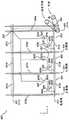
本公开的各个实施例的潜在优点中的一些,诸如薄度、亮度和功率效率,尤其可以用于便携式装置,尽管本公开的实施例的用途不限于便携式装置。图1A-图1C示出其中可以实现根据本公开的实施例的集成触摸屏的示例系统。图1A说明包括集成触摸屏124的示例移动电话136。图1B说明包括集成触摸屏126的示例数字媒体播放器140。图1C说明包括集成触摸屏128的示例个人计算机144。Some of the potential advantages of various embodiments of the present disclosure, such as thinness, brightness, and power efficiency, are particularly applicable to portable devices, although the use of embodiments of the present disclosure is not limited to portable devices. 1A-1C illustrate an example system in which an integrated touch screen according to embodiments of the present disclosure may be implemented. FIG. 1A illustrates an example
图1D-图1G说明根据本公开的实施例的包括示例集成触摸屏153的示例集成触摸屏系统150。参考图1D,触摸屏153包括显示像素155,显示像素155包括多功能电路元件。图1D示出一个显示像素155的放大图,其包括多功能电路元件157、159和161,这些多功能电路元件157、159和161可以操作为显示系统控制器170控制的显示系统的一部分且可以操作为触摸感应系统控制器180控制的触摸感应系统的触摸感应电路的一部分。显示像素155还包括多功能电路元件163,其可以操作为显示系统的显示电路、触摸感应系统以及功率系统控制器190控制的功率系统的一部分。显示像素155还包括单功能显示电路元件165以及单功能触摸感应电路元件167,在一些实施例中,该单功能显示电路元件165可以仅操作为显示电路的一部分,在一些实施例中,该单功能触摸感应电路元件167仅操作为触摸感应电路的一部分。1D-1G illustrate an example integrated
图1E-图1G说明包括不同操作阶段的触摸屏系统150的示例操作。图1E示出在显示阶段中的示例操作,其中显示像素155的电路元件可以操作为在触摸屏153上显示图像。在显示阶段中的操作例如可以包括例如通过使用开关169a-e从显示电路的电路元件电分离或断开触摸感应电路元件167而有效地配置显示像素155为显示配置。有效地配置显示像素的电路元件以操作为集成触摸屏的特定系统的电路的一部分例如可以包括:切换不同系统的线之间的连接;开启/关闭电路元件;改变电压线中的电压值;改变信号,诸如控制信号等。有效配置可以在触摸屏的操作中发生且可以至少部分地基于静态配置,即触摸屏的结构配置。结构配置例如可以包括显示像素的叠层中的结构的大小、形状、布置、材料组成等,诸如显示像素叠层中导电路径的数目和布置、诸如连接两个导电层的接触点的填充导体的通孔的永久连接、诸如其中导电材料在设计中已被去除的导电路径的一部分的永久断路等。1E-1G illustrate example operations of
显示系统控制器170可以分别通过多功能电路元件159和163以及显示系统电路元件165发射控制信号171、173和175以促使显示像素150的多功能电路元件157和161在触摸屏153上显示图像。在一些实施例中,控制信号171、173和175例如可以是选通信号、Vcom信号和数据信号。
图1F示出在触摸感应阶段中的示例操作,其中显示像素155的电路元件可以操作为感应触摸,操作包括例如通过电连接触摸感应电路元件167与开关169b和169c且使用开关169a和169d电断开显示系统电路元件165而有效地配置显示像素以用于触摸感应。触摸感应系统控制器180可以发射控制信号181且可以接收信息信号183和185。在一些实施例中,控制信号181例如可以是用于电容感应的驱动信号、用于光学感应的驱动信号等。在一些实施例中,信息信号183例如可以是用于电容、光学等感应的感应信号且信息信号185例如可以是触摸感应系统的反馈信号。FIG. 1F shows example operations in the touch sensing phase, in which circuit elements of
图1G示出在功率系统阶段中的示例操作,其中显示像素155的多功能电路元件163可以使用开关169c、169d和169e从显示系统和触摸感应系统电断开。功率系统控制器190可以通过多功能电路元件163发射信号192。信号192例如可以是指示功率系统的充电状态、电源电压等的信号。FIG. 1G illustrates example operation in the power system phase, where the
在本公开的一些实施例中,触摸感应系统可以基于电容。通过检测触摸像素中的每一个处的电容的变化且记录触摸像素的位置,触摸感应系统可以识别多个对象,且当这些对象在触摸屏上移动时确定对象的位置、压力、方向、速度和/或加速度。In some embodiments of the present disclosure, the touch sensing system may be based on capacitance. By detecting changes in capacitance at each of the touch pixels and recording the location of the touch pixels, a touch sensing system can identify multiple objects and determine the object's position, pressure, direction, velocity and/or as these objects move across the touch screen or acceleration.
举例而言,集成触摸感应系统的一些实施例可以基于自电容且一些实施例可以基于互电容。在基于自电容的触摸系统中,可以由形成对地的自电容的个体电极而形成每个触摸像素。当对象接近该触摸像素时,可以在对象和该触摸像素之间形成附加的对地电容。该附加的对地电容可以导致触摸像素可见的自电容的净增加。自电容中的这种增加可以由触摸感应系统检测和测量以当多个对象触摸触摸屏时确定它们的位置。在基于互电容的触摸系统中,触摸感应系统例如可以包括诸如驱动线和感应线的驱动区域和感应区域。在一个示例情况中,驱动线可以按行形成而感应线可以按列(例如正交)形成。触摸像素可以在行和列的交叉点设置。在操作中,行可以使用AC波形激励且互电容可以在触摸像素的行和列之间形成。当对象接近该触摸像素时,耦合在触摸像素的行和列之间的电荷中的一些可以耦合到该对象上。耦合在触摸像素上的电荷的这种减小可以导致行和列之间的互电容的净减小以及耦合在触摸像素上的AC波形的减小。电荷耦合的AC波形的这种减小可以被触摸感应系统检测和测量,以当多个对象触摸触摸屏时确定它们的位置。在一些实施例中,集成触摸屏可以是多触摸、单触摸、投影扫描、全成像多触摸或任意电容触摸的。For example, some embodiments of an integrated touch sensing system may be based on self capacitance and some embodiments may be based on mutual capacitance. In a self-capacitance-based touch system, each touch pixel may be formed by an individual electrode that forms a self-capacitance to ground. As an object approaches the touch pixel, additional capacitance to ground may be formed between the object and the touch pixel. This additional capacitance to ground can result in a net increase in self-capacitance visible to the touch pixel. This increase in self-capacitance can be detected and measured by the touch-sensing system to determine the location of multiple objects when they touch the touch screen. In a mutual capacitance based touch system, the touch sensing system may include, for example, drive regions and sense regions such as drive lines and sense lines. In one example case, the drive lines may be formed in rows and the sense lines may be formed in columns (eg, orthogonal). Touch pixels can be set at the intersection of rows and columns. In operation, the rows can be excited using an AC waveform and mutual capacitances can be formed between the rows and columns of touch pixels. When an object approaches the touch pixel, some of the charge coupled between the rows and columns of the touch pixel may couple to the object. This reduction in charge coupled on the touch pixels can result in a net reduction in mutual capacitance between rows and columns and a reduction in the AC waveform coupled on the touch pixels. This reduction in the charge-coupled AC waveform can be detected and measured by a touch sensing system to determine the location of multiple objects when they touch the touch screen. In some embodiments, the integrated touch screen may be multi-touch, single-touch, projection scanning, full imaging multi-touch, or any capacitive touch.
图2是说明根据本公开的实施例的示例集成触摸屏220的一个实施方式的示例计算系统200的框图。计算系统200例如可以包括在含有触摸屏的移动电话136、数字媒体播放器140、个人计算机144或任意移动或非移动计算设备中。计算系统200可以包括触摸感应系统,该触摸感应系统包括一个或多个触摸处理器202、外围设备204、触摸控制器206以及触摸感应电路(在下面更详细描述)。外围设备204可以包括但不限于随机存取存储器(RAM)或其他类型的内存或存储器、看门狗计时器等。触摸控制器206可以包括但不限于一个或多个感应通道208、通道扫描逻辑210和驱动器逻辑214。通道扫描逻辑210可以访问RAM 212,自主地从感应通道读取数据且提供用于感应通道的控制。另外,通道扫描逻辑210可以控制驱动器逻辑214以在可以选择性地应用于驱动触摸屏220的触摸感应电路的驱动区域的各个频率和相位产生激励信号216,如下面更详细描述。在一些实施例中,触摸控制器206、触摸处理器202和外围设备204可以集成到单个专用集成电路(ASIC)中。FIG. 2 is a block diagram of an
计算系统200还可以包括用于从触摸处理器202接收输出且基于该输出执行动作的主机处理器228。例如,主机处理器228可以连接到程序存储器232和诸如LCD驱动器234的显示控制器。主机处理器228可以使用LCD驱动器234以在触摸屏220上产生图像,诸如用户界面(UI)的图像,且可以使用触摸处理器202和触摸控制器206来检测触摸屏220上或其附近的触摸,诸如到显示的UI的触摸输入。触摸输入可以被存储在程序存储器232中的计算机程序使用以执行动作,所述动作包括但不限于移动诸如光标或指针的对象、滚动或平移、调节控制设置、打开文件或文档、查看菜单、做出选择、执行指令、操作连接到主机设备的外围设备、接听电话呼叫、拨出电话呼叫、终止电话呼叫、改变音量或音频设置、存储与电话通信相关的信息(诸如地址、频繁播打的号码、已接呼叫、未接呼叫)、登录计算机或计算机网络、允许授权个体访问计算机或计算机网络上的受限区域、装载与计算机桌面的用户优选布置相关的用户配置文件,允许访问网络内容、启动特定程序、加密或解码消息等。主机处理器228还可以执行可能与触摸处理无关的附加功能。
触摸屏220可以包括触摸感应电路,该触摸感应电路可以包括具有多个驱动线222和多个感应线223的电容感应介质。应当注意,如本领域技术人员所理解,术语“线”有时在此只是用于表示导电路径,且不限于严格线型的结构,而是包括改变方向的路径且包括不同大小、形状、材料等的路径。驱动线222可以由通过驱动接口224来自驱动器逻辑214的激励信号216驱动,且在感应线223中产生的所得的感应信号217可以通过感应接口225被发射到触摸控制器206中的感应通道208(也称为事件检测和解调电路)。以这种方式,驱动线和感应线可以是触摸感应电路的一部分,它们可以交互以形成电容感应节点,该电容感应节点可以被认为是触摸图片元件(触摸像素),诸如触摸像素226和227。这种理解方式在触摸屏220被看作捕获触摸的“图像”时是尤其有用的。换句话说,在触摸控制器206已经确定在触摸屏中每个触摸像素处是否检测到触摸之后,触摸屏中发生触摸处的触摸像素的图案可以被认为是触摸的“图像”(例如,触摸触摸屏的手指的图案)。The
图3是示出根据本公开的实施例的驱动线222和感应线223的示例配置的触摸屏220的更详细的视图。如图3所示,每个驱动线222可以由一个或多个驱动线片段301形成,这些驱动线片段可以通过连接205处的驱动线链路303电连接。驱动线链路303不电连接到感应线223,而是,驱动线链路可以通过旁路307而绕过感应线。驱动线222和感应线223可以电容性地交互以形成诸如触摸像素226和227的触摸像素。驱动线222(即,驱动线片段301和相应的驱动线链路303)和感应线223可以由触摸屏220中的电路元件形成。在图3的示例配置中,触摸像素226和227中的每一个可以包括一个驱动线片段301的一部分、感应线223的一部分以及另一驱动线片段301的一部分。例如,触摸像素226可以包括感应线的一部分311的一侧上的驱动线片段的右半部分309以及该感应线的部分311的相反侧上的驱动线片段的左半部分313。3 is a more detailed view of the
如上所述,电路元件例如可以包括可以在常规LCD显示器中存在的结构。应当注意,电路元件不限于诸如整个电容、整个晶体管等整个电路组件,而是可以包括电路的若干部分,诸如平行板电容的两个板中的仅一个。图4说明根据本公开的实施例的示例配置,其中公共电极(Vcom)可以形成触摸感应系统的部分触摸感应电路。公共电极是一些类型的常规LCD显示器(例如边缘场切换(FFS)显示器)的显示像素的叠层(即,形成显示像素的堆叠的材料层)中的显示系统电路的电路元件,其可以操作为显示系统的一部分以显示图像。在图4中示出的示例中,公共电极(Vcom)401(例如图1D的元件161)可以用作多功能电路元件,该多功能电路元件可以操作为触摸屏220的显示系统的显示电路且还可以操作为触摸感应系统的触摸感应电路。在该示例中,公共电极401可以操作为触摸屏的显示电路的公共电极,且当与其他公共电极组合时还可以作为触摸屏的触摸感应电路一起工作。例如,一组公共电极401可以在触摸感应阶段中一起操作为触摸感应电路的驱动线或感应线的电容部分。例如,通过将一区域的公共电极401电连接在一起、切换电连接等,触摸屏220的其他电路元件可以形成部分的触摸感应电路。一般而言,触摸感应电路元件中的每一个要么可以是多功能电路元件,要么可以是单功能电路元件,多功能电路元件可以形成部分的触摸感应电路且可以执行一个或多个其他功能,诸如形成部分的显示电路,单功能电路元件可以仅操作为触摸感应电路。类似地,显示电路元件中的每一个要么可以是多功能电路元件,要么可以是单功能电路元件,多功能电路元件可以操作为显示电路且执行一个或多个功能,诸如操作为触摸感应电路,单功能电路元件可以仅操作为显示电路。因此,在一些实施例中,显示像素叠层中的电路元件中的一些可以是多功能电路元件且其他电路元件可以是单功能电路元件。在其他实施例中,显示像素叠层的所有电路元件可以是单功能电路元件。As mentioned above, the circuit elements may include, for example, structures that may be present in conventional LCD displays. It should be noted that circuit elements are not limited to entire circuit components such as entire capacitors, entire transistors, etc., but may include several parts of the circuit, such as only one of the two plates of a parallel plate capacitor. 4 illustrates an example configuration in which a common electrode (Vcom) may form part of a touch-sensing circuit of a touch-sensing system, according to embodiments of the present disclosure. The common electrode is a circuit element of a display system circuit in a stack of display pixels (ie, the layers of material forming the stack of display pixels) of some types of conventional LCD displays, such as fringe field switching (FFS) displays, that may operate as Display part of the system to display the image. In the example shown in FIG. 4 , common electrode (Vcom) 401 (eg,
另外,尽管此处的示例实施例可以将显示电路描述为在显示阶段中操作,且将触摸感应电路描述为在触摸感应阶段中操作,应当理解,显示阶段和触摸感应阶段可以例如部分或完全交叠地同时操作,或者显示阶段和触摸阶段可以在不同的时间操作。而且,尽管此处的示例实施例将某些电路元件描述为多功能的且将其他电路元件描述为单功能的,应当理解,在其他实施例中,电路元件不限于特定功能性。换句话说,此处一个示例实施例中描述为单功能电路元件的电路元件在其他实施例中可以配置为多功能电路元件,且反之亦然。Additionally, while example embodiments herein may describe the display circuit as operating in the display phase and the touch-sensing circuit as operating in the touch-sensing phase, it should be understood that the display phase and the touch-sensing phase may, for example, partially or fully intersect. The stacks can be operated simultaneously, or the display phase and the touch phase can operate at different times. Furthermore, although the example embodiments herein describe some circuit elements as multifunctional and other circuit elements as single function, it should be understood that in other embodiments, the circuit elements are not limited to a particular functionality. In other words, circuit elements described herein as single-function circuit elements in one example embodiment may be configured as multi-function circuit elements in other embodiments, and vice versa.
例如,图4示出分组在一起的公共电极401以形成一般分别对应于驱动线片段301和感应线223的驱动区域片段403和的感应区域405。将显示像素的多功能电路元件分组到一个区域中可以意味着共同操作显示像素的多功能电路元件以执行区域的公共功能。分组到功能区域可以通过一个方法或方法的组合达成,例如,通过系统的结构化配置(例如,物理断路和旁路、电压线配置)、系统的操作配置(例如,开启/关闭电路元件,改变电压线上的电压值和/或信号)等达成。For example, FIG. 4 shows
在一些实施例中,电路元件的分组可以实现为显示像素的布局,每个显示像素选自于一组有限数目的显示像素配置。在一些实施例中,触摸感应电路的特定功能可以通过具有可以执行该功能的配置的特定类型显示像素提供。例如,下面参考图17-图22描述的一个实施例可以包括可以共同连接到叠层的连接层中的一个或多个相邻像素的类型的显示像素、可以提供与叠层的其他层的接触的类型的显示像素,以及可以共同连接其他层中的一个或多个相邻像素的类型的显示像素。In some embodiments, the grouping of circuit elements may be implemented as a layout of display pixels, each display pixel being selected from a limited number of display pixel configurations. In some embodiments, a specific function of the touch sensing circuit may be provided by a specific type of display pixel having a configuration that can perform the function. For example, one embodiment described below with reference to FIGS. 17-22 may include display pixels of a type that may be commonly connected to one or more adjacent pixels in a connecting layer of the stack, may provide contact with other layers of the stack types of display pixels, and types of display pixels that can commonly connect one or more adjacent pixels in other layers.
在一些实施例中,区域例如可以是可重新配置的以允许像素被分组到不同大小、形状等的区域。例如,取决于例如环境噪声的变化、要从触摸屏感应的对象的大小和/或距离等,一些实施例可以包括可编程开关阵列以允许可重新配置的切换方案来将显示像素分组到不同大小的区域。可以允许进行分组的配置的其他方面可以不是可重新配置的,例如,显示像素叠层中的线中的物理中断是不可重新配置的。然而,通过包括诸如可编程开关、信号产生器等可重新配置的其他电路元件,包括物理中断的触摸屏配置例如仍可以允许将显示像素可重新配置地分组到不同大小、形状等的区域。In some embodiments, regions may be reconfigurable, for example, to allow pixels to be grouped into regions of different sizes, shapes, and the like. For example, some embodiments may include an array of programmable switches to allow a reconfigurable switching scheme to group display pixels into different sized area. Other aspects of the configuration that may allow for grouping may not be reconfigurable, eg, physical breaks in the lines in the display pixel stack are not reconfigurable. However, touch screen configurations that include physical interruptions, for example, may still allow for reconfigurable grouping of display pixels into areas of different sizes, shapes, etc., by including other circuit elements that are reconfigurable, such as programmable switches, signal generators, and the like.
触摸屏的显示像素的多功能电路元件可以以显示阶段和触摸阶段操作。例如,在触摸阶段中,公共电极401可以分组在一起以形成触摸信号线,诸如驱动区域和感应区域。在一些实施例中,电路元件可以分组为形成一种类型的连续触摸信号线和另一种类型的分段的触摸信号线。例如,图4示出其中驱动区域片段403和感应区域405对应于触摸屏220的驱动线片段301和感应线223的一个示例实施例。在其他实施例中,其他配置是可行的,例如,公共电极401可以分组在一起,使得每个驱动线均由连续驱动区域形成且每个感应线均由通过旁路驱动区域的连接而链接在一起的多个感应区域片段形成。在下面参考图11A-图11B描述示例显示阶段和示例触摸阶段中的操作的更多细节。The multifunctional circuit elements of the display pixels of the touch screen can operate in both a display phase and a touch phase. For example, in the touch phase,
图3的示例中的驱动区域在图4中示为包括显示像素的多个公共电极的矩形区域,且图3的感应区域在图4中示为包括延伸LCD的垂直长度的显示像素的多个公共电极的矩形区域。在一些实施例中,图4的配置的触摸像素例如可以包括显示像素的64×64个区域。然而,驱动和感应区域不限于示出的形状、取向和位置,而是可以包括根据本公开的实施例的任意合适的配置。应当理解,根据本公开的实施例,用于形成触摸像素的显示像素不限于上面描述的这些,而可以是任意大小或形状以允许触摸功能。The drive area in the example of FIG. 3 is shown in FIG. 4 as a rectangular area including a plurality of common electrodes of display pixels, and the sensing area of FIG. 3 is shown in FIG. 4 as a plurality of display pixels that extend the vertical length of the LCD The rectangular area of the common electrode. In some embodiments, the touch pixels of the configuration of FIG. 4 may include, for example, 64×64 areas of display pixels. However, the drive and sense regions are not limited to the shapes, orientations, and locations shown, but may include any suitable configuration in accordance with embodiments of the present disclosure. It should be understood that, according to embodiments of the present disclosure, display pixels used to form touch pixels are not limited to those described above, but may be of any size or shape to allow for touch functionality.
图5说明根据本公开的实施例可以用于将公共电极401分组到图4中示出的区域且链接驱动区域片段以形成驱动线的导线的示例配置。一些实施例可以包括其他区域,诸如驱动线之间和/或驱动线和感应线之间的接地区域,如图13中示出的示例实施例所示。5 illustrates an example configuration of wires that may be used to group
图5示出沿着x方向的多个xVom线501和沿着y方向的多个yVCom线503。在该实施例中,公共电极401的每行可以具有相应的xVCom线501且公共电极401的每列可以具有相应的yVcom线503。图5还示出多个驱动区域片段403(通过虚线说明),其中每个驱动区域片段403可以形成为通过x-y-com连接505而连接在一起的一组公共电极401,如下面更详细描述,该x-y-com连接505将每个公共电极连接到该驱动区域片段中的xVcom线501和yVcom线503。通过驱动区域片段403行进的yVcom线503(诸如yVCom线503a)可以包括提供每个驱动区域片段从其他驱动区域片段(例如,给定驱动区域片段上面和下面的片段)的电隔离的中断509。中断509可以提供y断开(y方向中的电断开)。Figure 5 shows
每个驱动线511均可以由多个驱动区域片段403形成,该多个驱动区域片段403可以由公共电极401及其互连导线xVcom形成。具体而言,驱动线511可以通过使用xVom线501跨越感应区域405连接驱动区域片段403形成。如图5所示,第一驱动线511a可以由顶行的驱动区域片段403形成,且下一驱动线511b可以由下一行的驱动区域片段403形成。如下面更详细描述,xVcom线是使用旁路513绕过感应区域405中的yVcom线的导电路径。Each driving
图5还示出多个感应区域405(通过虚线说明)。每个感应区域405可以形成为通过y-com连接507连接在一起的一组公共电极401,该y-com连接可以连接感应区域405的每个公共电极到yVom线503之一。附加的连接(例如见图10)可以将每个感应区域405的yVcom线连接在一起。例如,附加的连接可以包括触摸屏220的边界中的开关,在操作的触摸阶段,所述开关可以将每个感应区域的yVcom线连接在一起。通过感应区域405行进的yVcom线503(诸如yVcom线503b)可以在y方向中电连接所有公共电极401,因此,这些感应区域的yVcom线不包括中断。以这种方式,例如,感应区域可以由彼此相连且连接到相应显示像素的电路元件的多个垂直公共电压线yVcom形成,由此在感应区域中形成由显示像素的电连接的电路元件组成的感应线512。在图5中示出的示例感应区域中,垂直公共电压线yVcom可以从水平公共电压线xVcom断开且可以跨过在水平公共电压线xVcom(在513)以形成用于电容触摸感应的结构。yVcom和xVcom上的这种跨越还可以在感应和驱动区域之间形成附加的寄生电容。Figure 5 also shows a plurality of sensing regions 405 (illustrated by dashed lines). Each
每个公共电极401可以对应于触摸屏220的显示像素,诸如显示像素515和517。在显示阶段中,公共电极401与其他显示像素组件一起操作为触摸屏220的显示系统的显示电路,以在触摸屏上显示图像。在触摸阶段中,公共电极401组可以操作为触摸屏220的触摸感应系统的触摸感应电路,以检测触摸屏上或附近的一个或多个触摸。Each
在触摸阶段的操作中,水平公共电压线xVcom 501可以发射激励信号以激励驱动线511且在受激励的驱动线和感应线512之间形成电场以形成触摸像素,诸如图3中的触摸像素226。当诸如手指的对象接近或触摸触摸像素时,该对象可以影响在驱动线511和感应线512之间延伸的电场,由此减小电容耦合到感应线的电荷的量。电荷的这种减小可以由感应通道感应到且与其他触摸像素的类似信息共同存储在存储器中以形成触摸的“图像”。During the touch phase of operation, the horizontal common
在一些实施例中,驱动线和/或感应线可以由其他结构形成,例如包括已经在典型LCD显示器中存在的其他结构(例如,将也用作典型LCD显示器中的电路元件的其他电极、导电和/或半导电的层、金属线,例如承载信号、存储电压等)、在非典型LCD叠层结构的LCD叠层中形成的其他结构(例如,其他金属线、板,其作用将基本用于触摸屏的触摸感应系统)以及在LCD叠层外部形成的结构(例如,诸如外部的基本透明的导电板、线和其他结构)。例如,触摸感应系统的一部分可以包括类似于已知触摸板交叠的结构。使用显示器中已经存在的结构部分或完整地形成触摸感应系统可以通过减小主要专用于触摸感应(典型地交叠显示器)的结构的量而潜在地增加触摸屏的图像质量、亮度等。In some embodiments, the drive lines and/or sense lines may be formed from other structures, including, for example, other structures that are already present in a typical LCD display (eg, other electrodes that would also be used as circuit elements in a typical LCD display, conductive and/or semiconducting layers, metal lines such as carrying signals, storing voltages, etc.), other structures formed in LCD stacks that are not typical LCD stack structures (eg, other metal lines, plates, whose role will be basically touch-sensing systems for touchscreens) and structures formed externally to the LCD stack (eg, such as external substantially transparent conductive plates, lines, and other structures). For example, a portion of a touch-sensing system may include structures similar to known touchpad overlays. Forming a touch-sensing system partially or completely using structures already present in the display can potentially increase the image quality, brightness, etc. of the touchscreen by reducing the amount of structure that is primarily dedicated to touch-sensing (typically overlapping the display).
在一些实施例中,例如,显示像素可以分组到驱动区域和感应区域之间和/或两个驱动之间的区域,且这些区域可以连接到地或虚拟的地以形成接地的区域,以进一步最小化驱动区域之间和/或驱动区域与感应区域之间的干扰。图13A-图13B示出根据本公开的实施例的区域的示例布局,包括驱动区域之间以及驱动区域和感应区域之间的接地区域。在其他示例中,垂直公共电压线中断可以省略且这些线在驱动区域之间完全共享。In some embodiments, for example, display pixels may be grouped into regions between a drive region and a sense region and/or between two drives, and these regions may be connected to ground or virtual ground to form grounded regions to further Minimize interference between drive regions and/or between drive and sense regions. 13A-13B illustrate example layouts of regions, including ground regions between drive regions and between drive regions and sense regions, according to embodiments of the present disclosure. In other examples, vertical common voltage line interruptions may be omitted and these lines are fully shared between drive regions.
从图5中可以看出,显示像素515可以被分组到感应区域405中,并且显示像素517可以被分组到驱动区域片段403中。图6-图8说明示出图5中的“方框A”中的显示像素515和517的更多细节的平面图和侧视图,且示出根据本公开的实施例的包括面内/层内示例中断/旁路以及面外/层外的示例中断/旁路的实例的一个示例配置。As can be seen in FIG. 5 , display
图6是图5中“方框A”的放大图,示出根据本公开的实施例的触摸屏220的显示像素515和517以及其他结构的进一步细节。显示像素515和517均可以包括公共电极401和三个显示像素电极601,分别用于在触摸屏的显示阶段中在子像素的晶体管609由选通线611上应用的电压而导通时提供颜色数据到所述子像素的对应于R数据线603、G数据线605和B数据线607的红色(R)子像素、绿色(G)子像素和蓝色(B)子像素。6 is an enlarged view of "Block A" in FIG. 5, showing further details of
在一些实施例中,可以使用其他类型的显示像素,诸如单色(例如,黑色和白色)显示像素、包括多于或少于三个子像素的显示像素、以诸如红外的不可见谱操作的显示像素等。不同的实施例可以包括具有不同大小、形状、光学属性的显示像素。一些实施例的显示像素可以彼此具有不同大小、形状和光学属性,且在一些实施例中,在触摸屏中使用的不同类型的显示像素可以提供不同的功能性。In some embodiments, other types of display pixels may be used, such as monochrome (eg, black and white) display pixels, display pixels comprising more or less than three sub-pixels, displays operating in the invisible spectrum such as infrared pixels, etc. Different embodiments may include display pixels with different sizes, shapes, and optical properties. The display pixels of some embodiments may have different sizes, shapes, and optical properties from each other, and in some embodiments, different types of display pixels used in touchscreens may provide different functionality.
图6还说明通过显示像素517行进的yVcom线503具有从相邻驱动区域片段分离显示像素517(以及显示像素517的驱动区域片段403,见图5)的中断509。中断509是面内中断的示例,其是基本在相同的平面(在这种情况中是yVcom线503行进的x-y平面)内行进的导电路径之间的电开路。类似地,中断509是层内中断的示例,其是在相同层(如下所述,在这种情况下是第二金属层)中行进的导电路径之间的电开路的。尽管很多层内中断也可以是面内中断,但这不是必须的。例如,叠层中材料层的导电路径中的中断可以在不同叠层高度形成的层(即不同平面)的位置发生,且因而这种位置处的中断应是层内、面外中断,而不是层内、面内中断。6 also illustrates that the
另一方面,通过感应区域405的显示像素515行进的yVcom线503不包括中断,使得显示像素515可以在y方向中电连接到感应区域405的其他显示像素,即,该感应区域中的显示像素是y连接的。On the other hand, the
xVcom线501在x方向中行进通过显示像素515和517。如显示像素515的左上角处的R数据线603后面的xVcom的放大图所示,xVcom线501分别位于R、G和B数据线603、605和607后面。xVcom和yVcom线与显示像素515和517的公共电极401之间的连接在图6中的分解图中更详细地示出,图6还示出xVcom线501位于yVcom线503后面,且yVcom线503位于公共电极401后面。对于感应区域的显示像素515,显示像素515的y-com连接507的分解图示出该y-com连接是位于yVcom线503和显示像素的公共电极401之间的导线613(例如,填充有导电材料的通孔),且示出在xVcom线501和yVcom线503之间没有连接,即旁路513(且因此在xVcom线和公共电极之间没有连接)。作为旁路513的结果,显示像素515可以是x断开的或者在x方向中隔离,即,沿着x方向从相邻显示像素断开或隔离。在该示例实施例中,感应区域的yVcom线503的附加连接(诸如上述边界开关)电连接显示像素515的公共电极401到显示像素515左边的相邻感应区域显示像素的公共电极,因而旁路513从显示像素515右边的相邻驱动区域显示像素517“右断开”显示像素515(换句话说,显示像素515可以在正x方向中从显示像素x断开,即,正x断开)。The
旁路513是面外旁路的示例,其可以是在基本不同的面内行进的导电路径之间的电开路;在这种情况下,yVcom线503行进的x-y面可以不同于xVcom线501行进的x-y面。类似地,旁路513是层外旁路的示例,其可以是在不同层(如下所述,在这种情况下是yVcom 503的第二金属层和xVcom 501的第一金属层)中行进的导电路径之间的电开路。包括yVcom-公共电极连接、触摸屏边界中的yVcom-yVcom连接(用于相同感应区域的yVcom线)以及xVcom和yVcom线之间的旁路的这种配置是一个示例,该示例将感应区域中的显示器的电路元件分组在一起以形成用于触摸感应的感应线,且使用xVcom线来旁路该感应线,该xVcom线将通过感应区域彼此分离的驱动区域片段链接在一起以形成用于触摸感应的驱动线。
对于驱动区域片段的显示像素517,显示像素517的x-y-com连接505的分解图示出该x-y-com连接可以包括连接xVcom线到yVcom线的导线615以及连接yVcom线到公共电极的导线613之一。因而,驱动区域片段中的每个显示像素的公共电极可以电连接在一起,因为每个显示像素可以连接到垂直线(yVcom)(即y-连接)和水平线(xVcom)(即x连接)的相同导电栅格。在该示例配置中,公共电极、垂直线以及水平线可以在不同的基本共面的平面中取向且通过两组连接而连接在一起,一组连接垂直和水平线,且另一组连接垂直线和公共电极。包括垂直线中的中断的这种配置是一个示例,该示例将驱动区域片段中的显示器的电路元件分组在一起以形成驱动线的触摸感应电路,该驱动线可以通过旁路居间感应线的驱动线链路被链接到其他驱动线片段。For
图7-图8是分别说明显示像素515叠层的一部分和显示像素517叠层的一部分的剖面图。图7示出显示像素515沿着图6中的7-7’的箭头线的剖面图。图7包括在第一金属层(M1)中形成的选通线611和xVcom线501、B数据线607、漏极701以及在第二金属层(M2)中形成的yVcom线503。该图还包括由诸如ITO的透明导体形成的公共电极401和显示像素电极601。公共电极401可以通过可以使用导电材料填充的电介质层707a中的通孔,导电通孔703被电连接到yVcom线503,该导电通孔703是图6的导线613的一个示例。图7还示出xVcom 501和yVcom 503之间的旁路513(无连接)。就这方面而言,旁路513可以被看作是分离xVcom501和yVcom 503的结构,其可以包括电介质层707b的一部分。栅极绝缘层705可以包含诸如SiO2、SiNx等电介质材料。液晶层可以布置在像素电极上方,接着是滤色片,且偏振器可以布置在叠层的顶部和底部上(未示出)。参考图7,从上面观看触摸屏。7-8 are cross-sectional views illustrating a portion of the stack of
图8示出显示像素517沿着图6中的8-8’的箭头线的剖面图。图8与图7相同,只不过图8中的导电通孔801代替了图7中的旁路513。因而,xVcom 501可以电连接到驱动区域片段显示像素517中的yVcom503。因而,图6中的导线615在该示例叠层中可以是填充了导体的通孔。FIG. 8 shows a cross-sectional view of the
结合在一起,图7-图8说明在一些实施例中根据本公开的实施例使用面外/层外中断/旁路可如何提供高效的方式来形成包括多功能电路元件的多功能触摸感应LCD结构的一个示例。在这种情况下,在一些实施例中,在不同面/层中导电路径之间形成的连接/旁路可以允许多功能配置的设计中的更多选项,且可以潜在地减小添加的结构的数目,例如,线的数目,否则需要添加线以形成相同面/层中的旁路。就这方面而言,例如,可以通过简单地在显示像素叠层的不同面/层中形成导电路径而可以方便地形成一些实施例中的y断开和/或x断开。同样,在一些实施例中,可以使用不同面/层之间的导电路径来连接不同面/层中的导电路径而方便地形成y连接和/或x连接。尤其是,这可以允许现有的LCD设计更容易地被修改以添加根据本公开的实施例的集成触摸功能性。就这方面而言,面内/层内和面外/层外中断和旁路的选择性使用可以允许现有LCD设计中的更多结构用作触摸感应系统中的电路元件,且可以减小需要对诸如掩膜、掺杂、沉积等现有制造工艺做出改变的数目。Taken together, FIGS. 7-8 illustrate how in some embodiments the use of out-of-plane/out-of-layer interrupts/bypasses can provide an efficient way to form multi-function touch-sensitive LCDs including multi-function circuit elements in accordance with embodiments of the present disclosure An example of a structure. In this case, in some embodiments, connections/bypasses formed between conductive paths in different faces/layers may allow more options in the design of multifunctional configurations, and may potentially reduce added structure , for example, the number of lines, otherwise lines need to be added to form bypasses in the same face/layer. In this regard, for example, y-breaks and/or x-breaks in some embodiments may be conveniently formed by simply forming conductive paths in different sides/layers of the display pixel stack. Also, in some embodiments, conductive paths between different planes/layers may be used to connect conductive paths in different planes/layers to conveniently form y-connections and/or x-connections. In particular, this may allow existing LCD designs to be more easily modified to add integrated touch functionality in accordance with embodiments of the present disclosure. In this regard, the selective use of in-plane/in-layer and out-of-plane/out-of-layer interrupts and bypasses can allow more structures in existing LCD designs to be used as circuit elements in touch-sensing systems, and can reduce The number of changes that need to be made to existing manufacturing processes such as masking, doping, deposition, etc.
将参考图9-图12B描述示例触摸屏的进一步细节和操作多功能触摸屏LCD电路元件的示例方法。图9是根据本公开的实施例的包括多个子像素的示例触摸屏900的部分电路图。和上述示例实施例一样,触摸屏900的子像素可以被配置成使得它们能够具有作为LCD子像素和触摸传感器电路元件的多功能性。即,子像素可以包括电路元件,该电路元件可以操作为显示像素的LCD电路的一部分且可以操作为触摸感应电路的电路元件。以这种方式,触摸屏900可以操作为具有集成触摸感应功能的LCD。图9示出触摸屏900的子像素901、902和903的细节。在该示例实施例中,每个子像素可以是红色(R)、绿色(G)或蓝色(B)子像素,所有三个R、G和B子像素的组合形成一个彩色显示像素。尽管该示例实施例包括红色、绿色和蓝色子像素,子像素可以基于光的其他颜色或电磁辐射的其他波长(例如红外),或者可以基于单色配置。Further details of example touchscreens and example methods of operating the multifunction touchscreen LCD circuit elements will be described with reference to FIGS. 9-12B. FIG. 9 is a partial circuit diagram of an
子像素902可以包括具有栅极955a、源极955b和漏极955c的薄膜晶体管(TFT)955。子像素902还可以包括公共电极(Vcom)957b,其例如可以是在子像素901、902和903之间共享的基本导电的材料的连续板,诸如图6中示出的公共电极401。子像素902还可以包括可以与公共电极957b共同操作为显示系统电路的一部分的像素电极957a。像素电极957a例如可以是图6-图8中示出的像素电极601。触摸屏900可以操作为FFS显示系统,其中每个子像素的像素电极和公共电极产生应用于该子像素的液晶的边缘场,且还可以形成该子像素的存储电容。子像素902可以包括由像素电极957a和公共电极957b形成的存储电容957。子像素902还可以包括用于绿色(G)数据的数据线即Gdata线917的一部分917a,和选通线913的一部分913b。栅极955a可以连接到选通线部分913b,且源极955b连接到Gdata线部分917a。像素电极957a可以连接到TFT 955的漏极955c。
子像素901可以包括具有栅极905a、源极905b和漏极905c的薄膜晶体管(TFT)905。子像素901还可以包括像素电极907a,该像素电极907a可以与公共电极957b共同操作以产生用于子像素的边缘场且形成存储电容907。子像素901还可以包括用于红色(R)数据的数据线Rdata线915的一部分915a,以及选通线913的一部分913a。栅极905a可以连接到选通线部分913a,且源极905b可以连接到Rdata线部分915a。像素电极907a可以连接到TFT 905的漏极905c。子像素901和902例如可以包括常规LCD子像素的大部分或所有结构。The
子像素903可以包括具有栅极975a、源极975b和漏极975c的薄膜晶体管(TFT)975。子像素903还可以包括像素电极977a,该像素电极977a可以与公共电极957b共同操作以产生用于子像素的边缘场且形成存储电容977。子像素903还可以包括用于蓝色(B)数据的数据线Bdata线919的一部分919a,以及选通线913的一部分913c。栅极975a可以连接到选通线部分913c,且源极975b可以连接到Bdata线部分919a。像素电极977a可以连接到TFT 975的漏极975c。不像子像素901和902,子像素903还可以包括在y方向中行进的公共电压线yVcom925的一部分925a、以及连接点929。在其他实施例中,yVcom可以行进通过红色子像素或绿色子像素而不是蓝色子像素。诸如上面参考图6描述的y-com连接507或x-y-com连接505之类的连接可以在连接点929形成,例如以连接公共电极957b到yVcom 925(其垂直行进通过其他显示像素)、连接公共电极957b到yVcom 925和xVcom 921(其水平行进通过其他像素)等。以这种方式,例如,公共电极957b可以与其他显示像素的公共电极连接以形成连接的公共电极的区域。
如上面在一些示例实施例中所述,形成分离区域的一种方式是通过在水平和/或垂直公共线中形成中断(开路)。例如,yVcom 925可以具有如图9所示的可选中断,其可以允许该中断上面的子像素与该中断下面的子像素隔离,即,该子像素可以是底部断开的。x断开可以通过在连接点929处形成y-com连接而不是x-y-com连接而形成,因而,从公共电极957b断开xVcom 921。在一些实施例中,xVcom 921可以包括中断,其可以允许该中断右边的子像素与该中断左边的子像素隔离。其他配置可以允许显示像素电路元件如上所述使用通过感应线的旁路链接在一起的驱动线片段分组。As described above in some example embodiments, one way to form separate regions is by forming breaks (opens) in horizontal and/or vertical common lines. For example,
以这种方式,触摸屏900的公共电极可以共同分组以形成显示像素内的结构,该结构可以操作为触摸感应系统的触摸感应电路的一部分。例如,公共电极可以配置成形成驱动区域或感应区域,形成如上面针对一些实施例所描述的的旁路和链路等。就这方面而言,诸如公共电极、xVcom线等的电路元件可以操作为多功能电路元件。In this manner, the common electrodes of the
一般而言,触摸屏900可以配置成使得屏幕中的所有子像素的公共电极例如可以通过具有与多个水平公共电压线的连接的至少一个垂直公共电压线而连接在一起。另一触摸屏可以配置成使得不同组的子像素可以连接在一起以形成连接在一起的公共电极的多个分离区域。In general, the
将参考图10-图12B描述根据本公开的实施例的触摸感应操作。图10示出根据本公开的实施例的示例触摸屏的驱动区域1001和感应区域1003中的显示像素内的触摸感应电路中的一些的部分电路图。为清楚起见,图10包括使用虚线说明的电路元件以表示一些电路元件主要操作为显示电路而不是触摸感应电路的部分。另外,主要关于单个驱动显示像素1001a(例如,驱动区域1001的单个显示像素)和单个感应显示像素1003a(例如,感应区域1003的单个显示像素)描述触摸感应操作。然而,应当理解,驱动区域1001中的其他驱动显示像素可以包括与下面针对驱动显示像素1001a描述的相同的触摸感应电路,且感应区域1003中的其他感应显示像素可以包括与下面针对感应显示像素1003a描述的相同的触摸感应电路。因而,驱动显示像素1001a和感应显示像素1003a的操作的描述可以分别被认为是驱动区域1001和感应区域1003的操作的描述。A touch sensing operation according to an embodiment of the present disclosure will be described with reference to FIGS. 10-12B . 10 shows a partial circuit diagram of some of the touch sensing circuits within display pixels in the drive region 1001 and the sense region 1003 of an example touch screen in accordance with embodiments of the present disclosure. For clarity, FIG. 10 includes circuit elements illustrated using dashed lines to indicate that some circuit elements operate primarily as portions of display circuitry rather than touch sensing circuitry. Additionally, touch sensing operations are described primarily with respect to a single
参考图10,驱动区域1001包括多个驱动显示像素,该多个驱动显示像素包括驱动显示像素1001a。驱动显示像素1001a包括TFT 1007、选通线1011、数据线1013、xVcom线部分1015和yVcom线部分1017、像素电极1019和公共电极1023。图10示出公共电极1023,其通过xVcom线部分1015和yVcom线部分1017被连接到驱动区域1001中的其他驱动显示像素中的公共电极,以在驱动区域1001的显示像素内形成用于触摸感应的结构,这在下面更详细描述。感应区域1003包括多个感应显示像素,包括感应显示像素1003a。感应显示像素1003包括TFT 1009、选通线1012、数据线1014、yVcom线部分1016、像素电极1021以及公共电极1025。图10示出公共电极1025,其通过例如可以在触摸屏的边界区域中连接的yVcom线部分1016被连接到感应区域1003中的其他感应显示像素中的公共电极,以在感应区域1003的显示像素内形成用于触摸感应的结构,这在下面更详细描述。Referring to FIG. 10 , a driving region 1001 includes a plurality of driving display pixels including a driving
在触摸感应阶段中,应用到xVcom线部分1015的驱动信号在驱动区域1001的连接的公共电极1023的结构和连接到诸如电荷放大器1026的感应放大器的感应区域1003的连接的公共电极的结构之间产生电场。电荷注入到感应区域1003的连接的公共电极的结构中,且电荷放大器1026将电荷注入转换成可以测量的电压。注入的电荷的量以及所得的测量电压可以取决于诸如手指1027的触摸对象与驱动和感应区域的靠近度。以这种方式,测量的电压可以提供对触摸屏上或触摸屏附近的触摸的指示。In the touch sensing phase, the drive signal applied to the
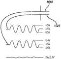
图11A示出在示例LCD或显示阶段以及在示例触摸阶段中通过xVcom 1015应用到包括驱动显示像素1001a的驱动区域1001的驱动显示像素的示例信号。在LCD阶段中,xVcom1015和yVcom 1017可以使用2.5V+/-2.5V的方波信号驱动以执行LCD反转。LCD阶段的持续时间是12ms。FIG. 11A shows example signals applied by
在触摸阶段中,xVcom 1015可以使用诸如正弦信号、方波、三角波等AC信号驱动。在图11A中示出的示例中,xVcom可以使用每个持续200微秒的15至20个连续激励相位驱动,而如图11B所示,yVcom 1016维持在电荷放大器1026的虚拟接地处。这种情况下驱动信号可以是2.5V+/-2V的方波或正弦信号,每一个具有相同的频率和要么为0度要么为180度(对应于图11A中的“+”和“-”)的相对相位。触摸阶段的持续时间是4ms。During the touch phase, the
图12A示出在触摸阶段中公共电极1023的操作的细节。尤其是,因为由公共电极1023和像素电极1019形成的存储电容的电容远高于系统中的其他电容(即,各个导电结构之间以及公共电极和手指1027之间的寄生电容),应用于公共电极1023的2.5V+/-2V的正弦驱动信号的几乎全部(约90%)的AC分量也应用于像素电极1019。因而,公共电极1023和像素电极1019之间的电压差可以保持很小,且液晶将经历由于触摸激励的最小电场变化,且维持其电荷状态和它在LCD阶段中设置得一样。在LCD的显示阶段操作中,公共电极1023和1025可以典型地充电到0或5V DC(方波2.5+/-2.0V)。然而,在触摸模式中,驱动区域1023中的公共电极使用2V幅度的叠加正弦信号充电到2.5V的DC电压。类似地,感应区域1025中的公共电极可以在2.5V的DC电平处保持在电荷放大器1026的虚拟接地处。在触摸阶段中,驱动区域1001中的公共电极1023上的正弦信号可以传递到感应区域1003的公共电极1025。由于驱动和感应区域中的公共像素电极之间的高度耦合,公共电极上的90%的电压变化被传递到相应的像素电极,因此,在执行触摸感应的同时最小化在显示阶段中存储的图像电荷的干扰。以这种方式,通过形成用于电容触摸感应的结构而不影响LCD图像,驱动和感应区域的公共电极可以操作为触摸感应电路的电路元件。FIG. 12A shows details of the operation of the
同时,公共电极和像素电极配置成操作为触摸感应电路的电路元件,上述电极可以继续操作为LCD系统的部分。如图12A-图12B所示,尽管像素电极1021的结构的电压各自在约+/-2V处被调制,像素电极1021和公共电极1025之间的相对电压基本保持在恒定值+/-0.1V。该相对电压是用于LCD操作的显示像素的液晶看到的电压,且其幅度可以确定图像的灰度值(例如在图12A中,该相对电压是2V)。在触摸(感应)阶段中相对电压中的0.1V的AC变化对于LCD应具有可接受的低影响,尤其因为该AC变化将典型地具有高于液晶的响应时间的频率。例如,激励信号频率且因此AC变化的频率将典型地大于100kHz。然而,液晶的响应时间典型地小于100Hz。因此,公共和像素电极用作触摸系统中的电路元件的功能不应与LCD功能相干扰。While the common and pixel electrodes are configured to operate as circuit elements of the touch sensing circuit, the electrodes may continue to operate as part of the LCD system. As shown in FIGS. 12A-12B , although the voltages of the structures of the
现在参考图10、图11B和图12B,现在将描述感应区域1003的示例操作。图11B示出在上述LCD和触摸阶段中通过yVcom 1016施加到包括显示像素1003a的感应区域的显示像素的信号。与驱动区域一样,yVcom 1016使用2.5V+/-2.5V的方波信号驱动,以在LCD阶段中执行LCD反转。在触摸阶段中,yVcom 1016连接到电荷放大器1026,其将电压保持在2.5V的虚拟地或其附近。因此,像素电极1021也保持在2.5V。如图10所示,边缘电场从公共电极1023传播到公共电极1025。如上所述,边缘电场通过驱动区域在约+/-2V处被调制。当这些场被像素电极1021接收时,大多数信号被传输到公共电极1025,因为显示像素1003a具有与显示像素1001a相同或类似的寄生电容和存储电容。Referring now to Figures 10, 11B and 12B, an example operation of the sensing region 1003 will now be described. FIG. 11B shows the signals applied by
因为yVcom 1016连接到电荷放大器1026且保持在虚拟地处,注入到yVcom 1016的电荷将产生电荷放大器的输出电压。该输出电压为触摸感应系统提供触摸感应信息。例如,当手指1027靠近边缘场时,它导致场中的干扰。该干扰可以被触摸系统检测为电荷放大器1026的输出电压中的干扰。碰撞到连接到TFT 1009的漏极的像素电极1021的大约90%的边缘场将被传输到电荷放大器1026。碰撞到直接连接到yVcom 1016的公共电极1025上的100%的电荷将被传输到电荷放大器1026。碰撞到每个电极上的电荷的比例将取决于LCD设计。对于非IPS,几乎100%的受到手指影响的电荷可碰撞到公共电极上,因为构图的CF板最靠近手指。对于IPS类型的显示器,该比例可以更接近50%,因为电极的每个部分具有面对手指的大约相等的面积(或者1/4比3/4)。对于一些子类型的IPS显示器,像素电极是不共面的,且大多数面向上的区域贡献于公共电极。Because
图13A示出根据本公开的实施例在触摸屏的触摸阶段中被分组成在触摸感应系统中起作用的的区域的多功能显示像素的另一示例配置。图13B示出具有图13A的接地区域的触摸屏的更详细的视图。如图13A-图13B所示,显示像素的区域例如可以在驱动区域和感应区域之间形成,且该区域可以接地到真正的地以形成驱动感应接地区域1301。图13A-图13B还示出两个驱动区域之间的显示像素的类似分组,其同样可以接地以形成驱动-驱动接地区域1303。接地区域和其他区域例如可以从诸如导线部分的栅格的连接结构形成。例如,图13A-图13B示出包括面内/层中断(y断开)1305和面内/层中断(x断开)1309的水平和垂直导电路径的接地区域连接栅格1304。链接驱动区域的线可以使用面外/层外旁路1308旁路接地区域和感应区域。在图13A-图13B的示例配置中,驱动-感应接地区域1301通过连接1310电连接到驱动-驱动接地区域1303,且所有接地区域可以通过在触摸屏的一个边界处的复用器1311接地到单个地1313。13A illustrates another example configuration of multi-function display pixels grouped into regions that function in a touch-sensing system during a touch phase of a touch screen in accordance with embodiments of the present disclosure. Figure 13B shows a more detailed view of the touch screen with the ground area of Figure 13A. As shown in FIGS. 13A-13B , the area of the display pixel can be formed between the driving area and the sensing area, for example, and this area can be grounded to the true ground to form the driving
图13B示出接地区域连接栅格1304可以通过连接1310连接接地区域1301和1303的公共电极,同时使用面内中断1305(y断开)和面内中断1309(x断开)维持从其他区域电分离。感应区域的公共电极可以类似地与栅格相连。图13B还示出驱动区域的公共电极可以由通过连接1323连接的导线的不同栅格形成以形成驱动区域连接栅格1321。驱动区域连接栅格的水平线可以旁路接地区域和感应区域,旁路导电路径1325使用例如面外旁路1308行进通过接地和感应区域,以防止驱动区域与接地和感应区域之间的电接触。旁路导电路径例如可以是在下面更详细描述的驱动隧道。在图13A-图13B的示例配置中,接地区域1301和1303均是两个显示像素宽;然而,接地区域的宽度不限于两个显示像素,而可以是更少或更多的显示像素宽。同样,尽管图13A-图13B示出连接到驱动-感应接地区域的驱动-驱动接地区域,在其他实施例中,接地区域可以从其他接地区域电分离。在其他实施例中,接地区域可以接地到其他类型的地,诸如AC地。接地区域1301和1303可以帮助减小可能在驱动和感应区域之间和/或驱动和驱动区域之间形成的静电电容。减小触摸系统配置中的这种静电电容可以改善触摸屏的精度和功耗。13B shows that the ground
图14A-图16C说明根据本公开的实施例的包括第三金属(M3)层的显示像素的多功能电路元件的另一示例配置,且说明用于根据本公开的实施例制造显示像素的示例方法。仅仅为了便于比较,图14A-图16C以并排的视图示出三个不同显示像素的示例设置,且并不旨在暗示着显示像素的特定顺序。图14A-图14C示出驱动区域中的示例显示像素1401,诸如参考图5-图6中描述的显示像素517。图15A-图15C示出具有驱动隧道的感应区域中的示例显示像素1501,诸如参考图5-图6描述的像素515。图16A-图16C示出没有驱动隧道的感应区域中的示例显示像素1601。在下面的描述中,仅仅为清楚起见,参考单个显示像素描述对于所有显示像素1401、1501和1601相同的工艺和结构。FIGS. 14A-16C illustrate another example configuration of a multifunctional circuit element of a display pixel including a third metal (M3) layer according to embodiments of the present disclosure, and illustrate examples for fabricating display pixels according to embodiments of the present disclosure method. 14A-16C illustrate an example arrangement of three different display pixels in side-by-side views for ease of comparison only, and are not intended to imply a particular order of display pixels. 14A-14C illustrate an
图14A、图15A和图16A示出工艺的较早期阶段,该工艺早期阶段包括形成包括晶体管的电路元件的多晶硅层的第一阶段。第二阶段包括在所有显示像素的M1层中形成选通线,且在显示像素1401和1501的M1层中形成xVcom线。显示像素1401的xVcom线包括在左侧的扩展部分以允许到yVcom线的连接。显示像素1501的xVcom线用作旁路感应区域中的其他导电路径的驱动隧道,因为在xVcom线和感应区域的其他导电路径之间不形成连接(即,存在旁路)。接下来,在显示像素的晶体管电路元件上形成包括连接的连接层(CON1)。显示像素1401包括扩展xVcom部分上的附加连接。数据线在显示像素的M2层中形成,且显示像素1401的M2层包括yVcom线。Figures 14A, 15A, and 16A illustrate earlier stages of a process that include a first stage of forming a polysilicon layer of circuit elements including transistors. The second stage includes forming gate lines in the M1 layers of all display pixels, and forming xVcom lines in the M1 layers of
图14B、图15B和图16B示出工艺的中间阶段。用于参照,也示出M2层。形成连接晶体管漏极到像素电极的第二连接层(CON2)。显示像素1401包括在CON2中连接yVcom到公共电极的另一连接。接下来,形成例如ITO的公共电极。Figures 14B, 15B and 16B illustrate intermediate stages of the process. For reference, the M2 layer is also shown. A second connection layer (CON2) is formed to connect the drain electrode of the transistor to the pixel electrode.
图14C、图15C和图16C示出工艺的最后阶段,且示出源于原先工艺的Vcom以做参考。形成第三金属(M3)层。如图所示,显示像素1401的M3层不同于显示像素1501和1601的M3层。感应区域显示像素1501和1601的M3层配置包括连接到上面和下面的显示像素的垂直线,因而允许感应区域显示像素在y方向中被连接而不使用yVcom线。在驱动区域显示像素1401中模仿该M3结构可帮助减小触摸屏的视觉不协调性,该视觉不协调性可能源于感应区域中的附加金属。形成第三连接层(CON3)且然后在所有显示像素上形成显示像素电极。Figures 14C, 15C and 16C show the final stage of the process and show the Vcom from the previous process for reference. A third metal (M3) layer is formed. As shown, the M3 layer of
结合在一起,图14A-图14C示出类似于上述显示像素517的配置成用于驱动区域的显示像素1401。显示像素1401包括第一金属(M1)层中的选通线1403和xVcom线1405以及第二金属(M2)层中的yVcom线1407和数据线1409。显示像素1401可以包括诸如x-y-com连接1411的连接,诸如上述连接505。x-y-com连接1411连接xVcom线1405、yVcom线1407与公共电极(Vcom)1413。Taken together, FIGS. 14A-14C illustrate a
结合在一起,图15A-图15C示出类似于上述显示像素515的配置成用于感应区域的触摸屏显示像素1501。显示像素1501包括M1层中的选通线1503和xVcom线1505以及M2层中的数据线1507。因为xVcom线1505在叠层的下层(M1)中形成,且因为在xVcom和yVcom之间不提供连接,xVcom线通过感应区域显示像素1501水平地“隧穿”而不连接到感应区域的公共电极(Vcom)1513。这是驱动隧道的一个示例,其可以通过导电路径连接驱动区域,该导电路径通过另一类型的区域(诸如感应区域)的显示像素叠层行进,同时旁路该区域,即不电接触旁路区域的显示像素叠层中的触摸感应电路元件。同样,在其他实施例中,可以使用其他类型的隧道,诸如连接感应区域的感应隧道。图15C示出第三金属(M3)层部分地用作在x和y方向中电连接感应区域中的显示像素电路元件的连接结构,如连接栅格1509所示。注意,尽管yVcom用在驱动像素电极1401中,在感应像素电极1501和1601中不使用yVcom。而是,通过M3层提供y连接性。在一些实施例中,感应区域中的显示像素可以在水平方向中通过触摸屏的边界中的连接和开关被连接在一起。Taken together, Figures 15A-15C illustrate a touch
结合在一起,图16A-图16C示出显示像素1601,显示像素1601与显示像素1501相同,只不过显示像素1601不包括驱动隧道。如图16C中的连接栅格1603所示,显示像素1601不包括M3层中的连接结构以电连接感应区域中的显示像素电路元件。Taken together, FIGS. 16A-16C illustrate
图17-图23说明根据本公开的实施例的包括第三金属(M3)层的另一配置的显示像素的其他示例配置、用于制造显示像素的示例方法、示例触摸像素布局以及示例触摸屏。与上面的图14A-图16C一样,仅仅为了便于比较,图17-图20说明不同制造阶段中显示像素的示例组的并排视图。图21A和图21B说明根据本公开的实施例的一个示例的触摸像素的显示像素的示例布局。图21C和21D说明根据本公开的实施例的示例驱动隧道连接。图22-1和图22-2说明可以包括诸如图21A所示的示例触摸像素的示例触摸像素布局。17-23 illustrate other example configurations of display pixels including another configuration of a third metal (M3) layer, example methods for fabricating display pixels, example touch pixel layouts, and example touch screens in accordance with embodiments of the present disclosure. As with Figures 14A-16C above, and for ease of comparison only, Figures 17-20 illustrate side-by-side views of example groups of display pixels in different stages of manufacture. 21A and 21B illustrate example layouts of display pixels of touch pixels according to one example of an embodiment of the present disclosure. 21C and 21D illustrate example driven tunnel connections in accordance with embodiments of the present disclosure. 22-1 and 22-2 illustrate example touch pixel layouts that may include example touch pixels such as that shown in FIG. 21A.
参考图17-图20,用于一组8个示例显示像素(标记为A_像素,B_像素,…,H_像素)的显示像素叠层的示例制造工艺。如下面更详细地解释,该组中显示像素中的每一个是3种类型的显示像素之一:连接层类型,接触类型和隧道类型,如下面更详细描述。在下面的描述中,仅仅为了清楚起见,可以参考单个显示像素描述对于所有显示像素A-H公共的工艺和结构。Referring to Figures 17-20, an example fabrication process for a display pixel stack of a set of 8 example display pixels (labeled A_pixels, B_pixels, ..., H_pixels). As explained in more detail below, each of the display pixels in the set is one of 3 types of display pixels: a connection layer type, a contact type, and a tunnel type, as described in more detail below. In the following description, for clarity only, processes and structures common to all display pixels A-H may be described with reference to a single display pixel.
图17示出包括形成多晶硅层的第一阶段的示例工艺的较早期阶段,该多晶硅层包括晶体管1701的电路元件。第二阶段包括在所有显示像素的M1层中形成选通线1703,且在显示像素E-H的M1层中形成xVcom线1705。显示像素E-F的xVcom线包括在中间子像素的扩展部分1706以允许连接到公共电极。显示像素G-H的xVcom线用作旁路感应区域中的其他导电路径的驱动隧道,因为在xVcom线和感应区域的其他导电路径之间不形成连接(即,存在旁路)。接下来,在显示像素的晶体管电路元件以及扩展xVcom部分1706上形成包括连接1707的连接层(CON1)。在显示像素的M2层中形成数据线1709。FIG. 17 shows an earlier stage of an example process including a first stage of forming a polysilicon layer that includes the circuit elements of
图18示出示例工艺的中间阶段。用于参照,也示出M2层。形成第二连接层(CON2)以使用连接1801连接晶体管漏极到公共电极(Vcom)1805。显示像素E-F在CON2中包括连接xVcom 1705到公共电极1805的另一连接1803。接下来,例如可以由诸如ITO的基本透明的导体形成公共电极1805。Figure 18 shows an intermediate stage of an example process. For reference, the M2 layer is also shown. A second connection layer (CON2) is formed to connect the transistor drain to the common electrode (Vcom) 1805 using
图19示出工艺的最后阶段,且示出源于原先工艺的Vcom以做参考。在图19中示出的工艺中,形成第三金属(M3)层和第三连接层(CON3)。CON3层1905连接到显示像素电极。M3层形成为与Vcom1805电接触。每个显示像素的M3层包括两个垂直线1901和一个水平线1903。在一些实施例中,M3层可以用作与其他实施例中的yVcom线相同的目的。一般而言,在一些实施例中,M3层可以具有的某些优点在于它可以提供在其本身和数据/选通线之间耦合的相对低的交叉电容耦合。而且,在感应区域中,M3层的水平(x方向)连接可以用于将所有感应公共电极耦合在一起以增强y方向电荷感应。感应区域中公共电极的x-y连接可以在驱动区域中重复以用于均匀性。而且,通过在数据线上布置垂直M3线(y方向),可以实现增强的孔径率。因为驱动隧道甚至仍可以与M3层共同使用以旁路感应区域,因此M3层的水平(x方向)可以布置在驱动隧道上面和与其对准的任意xVcom层上面,从而增加孔径率。在不使用xVcom线的像素实施例中,激励驱动线信号可以馈入M3层。一般而言,激励驱动线信号可以馈入xVcom线和M3层之一或二者。取决于组的特定显示像素(即,A像素、B像素等),每个显示像素中的垂直线1901可以包括y断开或y连接。在图19中强调了B_像素的y连接和C_像素的y断开。取决于组的特定显示像素,每个显示像素中的水平线1903可以包括x断开或x连接。在图19中强调了A_像素的x连接和E_像素的x断开。显示像素A、F和H的M3层的垂直线1901和水平线1903延伸到该显示像素的边沿(顶、底、左和右),且可以潜在地连接显示像素A、F和H到每个方向中的相邻显示像素。因而,显示像素A、F和H提供x和y连接(x-con,y-con)。显示像素A、F和H被标记为x和y连接的显示像素,因为每个显示像素的水平线1903在右边和左边形成相邻显示像素之间的导电路径,且每个显示像素的垂直线1901在顶部和底部形成相邻显示像素之间的导电路径。然而,尽管显示像素A、F和H具有连接结构以在x方向和y方向均连接,显示像素不必连接到相邻显示像素,因为相邻显示像素中的一个或多个例如可以包括从像素A、F或H断开相邻显示像素的M3层中的断开。Figure 19 shows the final stage of the process and shows the Vcom from the previous process for reference. In the process shown in FIG. 19, a third metal (M3) layer and a third connection layer (CON3) are formed. The
显示像素B、E和G中的每一个中的M3层在垂直方向中完全延伸,但是不延伸到显示像素的右边沿。这些显示像素提供x断开和y连接(x-discon,y-con)。更具体而言,显示像素B、E和G是“右断开”,即它们不连接到它们右边的显示像素的M3层。同样,显示像素C的M3层提供x连接和y断开(x-con,y-discon),且更具体而言,像素C是“底部断开”的。显示像素D的M3层提供x和y断开(x-discon,y-discon),且更具体而言,像素D是“右和底部断开”的。应当注意,断开不限于右边和/或底部,但在显示像素的M3层的顶部、左边或者内部可以存在任意数目和组合的断开。The M3 layer in each of display pixels B, E, and G extends fully in the vertical direction, but does not extend to the right edge of the display pixels. These display pixels provide x-discon and y-connect (x-discon, y-con). More specifically, display pixels B, E and G are "right disconnected", ie they are not connected to the M3 layer of the display pixel to their right. Likewise, the M3 layer showing pixel C provides x-connect and y-discon (x-con, y-discon), and more specifically, pixel C is "bottom disconnected". The M3 layer showing pixel D provides x and y disconnects (x-discon, y-discon), and more specifically, pixel D is "right and bottom disconnected". It should be noted that the breaks are not limited to the right and/or bottom, but that there may be any number and combination of breaks on the top, left or inside the M3 layer of the display pixel.
图20示出示例工艺的甚至更稍后的阶段。示出M3和CON3层以作参考。在所有显示像素上形成显示像素电极2001和黑色掩膜(BM)2003。在图17-图20中,不像图5的实施例那样存在yVcom线连接。而是,M3层可以用作在x和y方向中连接公共电极的目的。然而,xVcom仍可以在一些像素(即,E、F、G、H)中使用以提供驱动隧道,即感应区域旁路。FIG. 20 shows an even later stage of an example process. The M3 and CON3 layers are shown for reference.
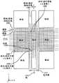
图21A和图21B示出用于一个示例触摸像素203的显示像素的示例布局。触摸像素2103包括64×64个显示像素的区域,显示像素中的每一个是根据图中示出的显示像素的图例的上述显示像素A-H中的一个。图21A还示出包括150(15×10)个触摸像素2103的示例布置的示例触摸屏2101。显示像素布局形成了显示像素的分组,这些显示像素可以基本对应于参考图4和图13在上面描述的的驱动区域片段、感应区域和接地区域。尤其是,显示像素的布局形成两个X区域(X1和X2)、两个Y区域(Y1和Y2)和一个Z区域。X1和X2区域例如可以是驱动区域片段的右半部分和另一驱动区域片段的左半部分,诸如分别是在图3中的右半部分309和左半部分313。Y区域例如可以是诸如图13中的驱动-感应接地区域1301的接地区域的部分。Z区域例如可以是诸如图3的感应线223的感应区域的一部分。图17-图20中示出的8个显示像素的组的特定配置与图21A和图21B中示出的特别设计像素布局一起形成可以在触摸感应系统中使用以检测触摸的电路元件的分组。21A and 21B illustrate example layouts of display pixels for one example touch pixel 203 . The touch pixel 2103 includes an area of 64×64 display pixels, each of which is one of the above-described display pixels A-H according to the legend of the display pixels shown in the figure. FIG. 21A also shows an example touch screen 2101 including an example arrangement of 150 (15×10) touch pixels 2103 . The display pixel layout forms groupings of display pixels, which may substantially correspond to the drive region segments, sense regions, and ground regions described above with reference to FIGS. 4 and 13 . In particular, the layout of the display pixels forms two X regions (X1 and X2), two Y regions (Y1 and Y2), and one Z region. The X1 and X2 regions may be, for example, the right half of a drive region segment and the left half of another drive region segment, such as
鉴于图17-图20以及图21A的图例,可以看出,来自列1-23的显示像素和来自行1-64的显示像素在M3层中连接在一起以形成驱动区域X1。接地区域Y1包括列24-25以及行1-64的显示像素。感应区域Z包括列26-39、行1-64。接地区域Y2包括列40-41和行1-64的显示像素。驱动区域X2包括列42-64、行1-64。In view of the legends of FIGS. 17-20 and FIG. 21A, it can be seen that display pixels from columns 1-23 and display pixels from rows 1-64 are connected together in the M3 layer to form drive region X1. Ground region Y1 includes display pixels of columns 24-25 and rows 1-64. Sensing zone Z includes columns 26-39, rows 1-64. Ground region Y2 includes display pixels of columns 40-41 and rows 1-64. The drive area X2 includes columns 42-64 and rows 1-64.
驱动区域X1和X2通过驱动隧道(旁路)2105的显示像素的电路元件电连接在一起。驱动隧道2105包括显示像素E、H、G和F。参考图20,从图中可以看出,显示像素E和F通过导电层Vcom ITO、CON2、M2和CON1提供M3层(在图20的接触点2005)之间的“接触”以与M1层中的xVconm相连。因而,显示像素E和F允许驱动区域的M3层通过隧穿旁路接地和感应区域(形成到达xVcom(M1)层的层外/面外旁路)。如图20所示,接触点2005可以位于显示像素E和F的中央子像素中。然而,接触点可以位于显示像素中的其他位置。The drive regions X1 and X2 are electrically connected together by the circuit elements of the display pixels of the drive tunnel (bypass) 2105 . Drive tunnel 2105 includes display pixels E, H, G, and F. Referring to Figure 20, it can be seen that display pixels E and F provide "contact" between the M3 layer (at
例如,图21说明根据本公开的实施例处于驱动区域2113的不同显示像素2111内的不同位置的示例驱动隧道接触点2109。在该示例中,驱动区域2113可以邻接感应区域2115。三个接触点2109可以连接3个显示像素2111到旁路感应区域2115的显示像素2119的驱动隧道2117。使用多个接触点例如可以减小驱动区域2113和驱动隧道2117之间的连接的阻抗。尽管图21C示出位于相邻显示像素2111中的三个接触点,接触点可以处于不同布置中且不需要在相邻显示像素中。另外,可以使用更多或更少的接触点。三个接触点2109可以位于其相应显示像素2111内的不同点处,例如,在每个显示像素的不同子像素中。For example, FIG. 21 illustrates example
图21D说明具有处于驱动区域2135的显示像素2133内的相同位置的驱动隧道接触点2129的其他示例。在该示例中,所有接触点2129位于其各自的显示像素2133中的相同子像素中,例如RGB显示像素的蓝色子像素中。接触点2129使用旁路感应区域2141的显示像素2139的驱动隧道2137连接显示像素2133。21D illustrates another example of having
显示像素G和H包括电路元件xVcom,且不包括xVcom和在下面更详细描述的触摸感应系统中操作的显示像素的其他电路元件中的任意一个之间的连接。因而,显示像素类型G和H是旁路接地和感应区域以将两个驱动区域(例如驱动区域X1和X2)连接在一起的隧穿连接的示例。Display pixels G and H include circuit element xVcom and do not include a connection between xVcom and any of the other circuit elements of the display pixel that operate in the touch-sensing system described in more detail below. Thus, display pixel types G and H are examples of tunneling connections that bypass ground and sense regions to connect two drive regions (eg, drive regions X1 and X2 ) together.
再次参考图17-图20,现在参考图21A和21B的示例显示像素布局更详细地描述显示像素的三个示例类型:连接层类型、接触类型和隧道类型。在该示例中,每个区域中的显示像素的公共电极主要通过M3层(此处也被称为连接层)连接在一起。A_像素、B_像素、C_像素和D_像素是连接层类型的显示像素,其可以提供通过连接层将显示像素的公共电极连接在一起的公共功能。尤其是,如上所述的垂直线1901和水平线1903电连接到显示像素的公共电极。连接层类型的显示像素的4个不同的M3层配置提供4种不同的方式来连接显示像素之间的M3层。A_像素可以连接所有相邻显示像素(顶、底、左和右)中的M3层。B_像素可以连接到顶部、底部和左边,但是提供从显示像素到右边的断开。C_像素可以连接到顶部、左边和右边,但是提供从下面显示像素的断开。D_像素可以连接到顶部和左边,但是提供从显示像素到右边和下面显示像素的断开。参考图21A,显示像素布局的大部分显示像素可以是A_像素,典型地可以位于区域的内部区域中以有效地连接所有相邻像素。Referring again to Figures 17-20, three example types of display pixels: connection layer type, contact type, and tunnel type are now described in more detail with reference to the example display pixel layouts of Figures 21A and 21B. In this example, the common electrodes of the display pixels in each area are mainly connected together by an M3 layer (also referred to herein as a connecting layer). A_pixels, B_pixels, C_pixels, and D_pixels are connection layer type display pixels that can provide a common function of connecting the common electrodes of the display pixels together through the connection layer. In particular,
B_像素、C_像素和D_像素可以位于区域的边界处,因为这些显示像素的x和y断开可以提供形成区域的边界的断开。例如,如图21A所示,右断开的B_像素可以以垂直线布置,以左右分离区域。如图21A所示,C_像素可以以水平线布置,以使得区域上下分离。D_像素可以位于区域的拐角中,以使得区域左右且上下分离。The B_pixels, C_pixels, and D_pixels may be located at the boundaries of the regions, since the x and y disconnects of these display pixels may provide the disconnects that form the boundaries of the regions. For example, as shown in FIG. 21A, the B_pixels that are disconnected on the right may be arranged in vertical lines to separate regions from left to right. As shown in FIG. 21A, the C_pixels may be arranged in horizontal lines so that the regions are separated up and down. D_pixels can be located in the corners of the regions so that the regions are separated left and right and up and down.
单独使用像素A-D,可以形成图21A中示出的驱动区域片段、感应线和接地区域。然而在本公开的一些实施例中,驱动区域片段通过旁路诸如接地区域和感应区域的其他区域的导电路径电连接在一起。接触类型的显示像素(即,E像素和F像素)以及隧道类型的显示像素(即,G像素和H像素)可以形成旁路其他区域的导电路径。接触类型的像素可以电连接或断开显示像素的叠层中的两个或更多导电层。此处描述的示例接触类型的显示像素包括M3层和xVcom线之间的连接,其可以在第一金属层(M1层)中形成。因而,通过连接驱动区域片段的连接层(M3层)到不同导电路径(M1层中的xVcom线),接触类型的像素形成面外/层外旁路。隧道类型的显示像素包括xVcom线,但是不包括xVcom线和诸如M3层的显示像素叠层的任意其他电路元件之间的连接。Using pixels A-D alone, the drive region segments, sense lines, and ground regions shown in FIG. 21A can be formed. In some embodiments of the present disclosure, however, the drive region segments are electrically connected together by conductive paths that bypass other regions, such as the ground region and the sense region. Contact-type display pixels (ie, E and F pixels) and tunnel-type display pixels (ie, G and H pixels) may form conductive paths that bypass other regions. Contact-type pixels can electrically connect or disconnect two or more conductive layers in a stack of display pixels. The example contact type display pixels described herein include connections between the M3 layer and the xVcom line, which may be formed in the first metal layer (M1 layer). Thus, the contact type pixels form out-of-plane/out-of-layer bypasses by connecting the connection layer (M3 layer) of the drive region segment to a different conductive path (xVcom line in M1 layer). A tunnel-type display pixel includes the xVcom line, but does not include the connection between the xVcom line and any other circuit elements of the display pixel stack, such as the M3 layer.
现在将更详细地描述旁路导电路径。如图21A和21B所示,触摸像素2103包括3个驱动隧道2105。每个驱动隧道2105包括以下模式的像素类型的显示像素:E、H、G、H,…,H、G、H、G、F。驱动隧道2105是旁路导电路径的一个示例。在驱动隧道2105的左端开始,旁路导电路径开始于E_像素,其包括连接层中的右断开以断开图21中驱动区域片段和接地区域之间的连接层。因此,E_像素的右断开导致两个驱动区域片段之间的连接层中的+x断开,且E_像素的面外/层外连接导致两个驱动区域片段之间的另一层(M1)中的x连接。The bypass conductive path will now be described in more detail. As shown in FIGS. 21A and 21B , the touch pixel 2103 includes three drive tunnels 2105 . Each drive tunnel 2105 includes display pixels of the following modes of pixel types: E, H, G, H, . . . , H, G, H, G, F. Drive tunnel 2105 is an example of a bypass conductive path. Beginning at the left end of the drive tunnel 2105, the bypass conductive path begins at E_pixel, which includes a right break in the connection layer to break the connection layer between the drive region segment and the ground region in FIG. 21 . Therefore, the right disconnection of the E_pixel results in a +x disconnection in the connection layer between the two drive area segments, and the out-of-plane/out-of-layer connection of the E_pixel results in another layer between the two drive area segments The x connection in (M1).
一旦形成与其他层的面外/层外连接,旁路导电路径使用隧道类型的显示像素行进通过其他区域(即,接地区域和感应区域)。隧道类型的显示像素均包括xVcom线且备选地包括x断开和x连接。更具体而言,G_像素包括右断开,且H_像素包括右连接。隧道类型的显示像素的x连接/断开例如可以允许多于一个的其他区域在两个驱动区域片段之间形成。尤其是,如图21所示,G_像素可以在B_像素的垂直列中形成以产生断开,以形成接地区域Y1和感应区域Z之间的边界、感应区域Z和接地区域Y2之间的边界以及接地区域Y2和驱动区域片段X2之间的边界。H_像素可以位于诸如接地区域和感应区域的其他区域的内部区域中,因为H_像素的连接层(M3层)连接到所有相邻像素,这类似于A像素。Once out-of-plane/out-of-layer connections to other layers are formed, bypass conductive paths travel through other regions (ie, ground and sense regions) using a tunnel-type display pixel. Tunnel-type display pixels each include xVcom lines and alternatively include xdisconnects and xconnects. More specifically, G_pixels include right disconnects, and H_pixels include right connections. The x-connection/disconnection of tunnel-type display pixels may, for example, allow more than one other area to be formed between the two drive area segments. In particular, as shown in FIG. 21, G_pixels can be formed in vertical columns of B_pixels to create disconnects to form boundaries between ground region Y1 and sensing region Z, and between sensing region Z and ground region Y2 and the boundary between the ground region Y2 and the drive region segment X2. H_pixels can be located in the inner regions of other regions such as the ground and sense regions because the connection layer (M3 layer) of the H_pixels is connected to all adjacent pixels, similar to the A-pixels.
图22-1和图22-2示出根据本公开的实施例的示例触摸像素布局和触摸屏2201。触摸屏2201包括连接2201到LCD电路(未示出)的LCD FPC(柔性印刷电路板)、在显示阶段中驱动显示像素的LCD、运送用于触摸屏的公共电压的Vcom线。触摸FPC包括以下线:向驱动区域发射驱动信号的r0-r14和r14-r0线、从感应区域接收感应信号的c0-c9线,连接到可以控制各种切换(诸如在触摸阶段中从连接所有数据线到虚拟地切换到在显示阶段中连接相应数据线到来自LCD驱动的相应数据输出、在触摸感应阶段中在感应区域之间切换等)的触摸开关(TSW)的tswX、tswY和tswZ(此处有时被称为“tswX,Y,Z”)线。触摸FPC还包括用于分别连接数据线和接地区域到虚拟地的g1和g0。包括驱动选通线的选通驱动器。22-1 and 22-2 illustrate an example touch pixel layout and touch screen 2201 according to embodiments of the present disclosure. The touch screen 2201 includes an LCD FPC (flexible printed circuit board) that connects 2201 to an LCD circuit (not shown), an LCD that drives the display pixels in the display phase, a Vcom line that carries the common voltage for the touch screen. The touch FPC consists of the following lines: r0-r14 and r14-r0 lines that transmit drive signals to the drive area, c0-c9 lines that receive sense signals from the sense area, connected to control various switching (such as connecting all The data lines are switched to virtual ground to the tswX, tswY and tswZ of the touch switches (TSWs) that connect the corresponding data lines to the corresponding data outputs from the LCD driver in the display phase, switch between sensing areas in the touch sensing phase, etc.) Sometimes referred to herein as the "tswX, Y, Z") line. The touch FPC also includes g1 and g0 for connecting the data line and the ground area to the virtual ground, respectively. Includes a gate driver that drives the gate lines.
图22-2还示出触摸屏2201的侧视图。该侧视图更详细地说明这些连接中的一些。例如,图22-2示出来自Y区域的M3连接允许这些区域接地到g0。来自Z区域的M3连接允许Z区域连接到c0-c9线。M2连接在触摸感应阶段中允许数据线接地到g1。22-2 also shows a side view of the touch screen 2201. This side view illustrates some of these connections in more detail. For example, Figure 22-2 shows that M3 connections from the Y regions allow these regions to be grounded to g0. The M3 connection from the Z region allows the Z region to connect to the c0-c9 lines. The M2 connection allows the data line to be grounded to g1 during the touch sensing phase.
图23是根据本公开的实施例包括高阻(R)屏蔽的示例触摸屏的侧视图。图23示出触摸屏2300的一部分,包括盖2301、粘合剂2302、偏振器2303、高阻(R)屏蔽2304、滤色器玻璃2305、驱动区域2309、感应区域2313、接地区域2315、TFT玻璃2316以及第二偏振器2317。液晶层可以布置在滤色器玻璃下面。诸如高R屏蔽2304的高阻屏蔽可以布置在CF玻璃和前偏振器之间,例如代替用于FFS LCD的低电阻率屏蔽层。高R屏蔽的薄层电阻例如可以是200M欧姆/平方~2G欧姆/平方。在一些实施例中,具有高阻屏蔽膜的偏振器可以用作高R屏蔽层,因而例如使用单个高R屏蔽偏振器代替偏振器2303和高R屏蔽2304。高R屏蔽可以帮助阻断显示器附近的低频/DC电压,防止干扰显示器的操作。同时,高R屏蔽可以允许诸如典型地用于电容触摸感应的高频信号穿透该屏蔽。因此,高R屏蔽可以帮助屏蔽显示,同时仍允许显示器感应触摸事件。高R屏蔽例如可以由极高电阻有机材料、碳纳米管等制成。23 is a side view of an example touch screen including a high resistance (R) shield according to an embodiment of the present disclosure. 23 shows a portion of a
图24是根据本公开的实施例的另一示例电容类型集成触摸屏2400的部分顶视图。该特定触摸2400基于自电容且因而它包括多个触摸感应区域2402,每个区域均代表触摸屏2400的平面中的不同坐标。触摸像素2402由包括多功能电路元件的显示像素2404形成,该多功能电路元件操作为显示电路的部分以在触摸屏2400上显示图像且操作为触摸感应电路的部分以感应触摸屏上或附近的触摸。在该示例实施例中,触摸感应电路和系统基于自电容操作,因而基于触摸像素2402中的电路元件的自电容操作。在一些实施例中,自电容和互电容的组合可以用于感应触摸。24 is a partial top view of another example capacitive-type integrated
尽管已经参考附图完全描述了本公开的实施例,应当注意,鉴于本说明书和附图,如本领域技术人员所显见,各种变化和修改包括但不限于组合不同实施例的特征、省略一个特征或多个特征等。Although the embodiments of the present disclosure have been fully described with reference to the accompanying drawings, it should be noted that various changes and modifications, including but not limited to combining features of different embodiments, omitting a feature or multiple features, etc.
例如,上述计算系统200的功能中的一个或多个可以通过存储在存储器(例如图2中的外围设备204中的一个)中的固件执行且通过触摸处理器202执行,或者存储在程序存储器232中且由主机处理器228执行。固件还可以存储和/或传输在任意计算机可读介质中以被指令执行系统、设备或装置(诸如基于计算机的系统、包含处理器的系统或可以从指令执行系统、设备或装置获取指令且执行指令的其他系统)使用或与之一同使用。在本文档的上下文中,“计算机可读介质”可以是可以包含或存储被指令执行系统、设备或装置使用或与之结合使用的程序的任意介质。该计算机可读介质可以包括但不限于电子、磁性、光学、电磁、红外或半导体系统、设备或装置、便携式计算机磁盘(磁性)、随机存取存储器(RAM)(磁性)、只读存储器(ROM)(磁性)、可擦除可编程只读存储器(EPROM)(磁性)、诸如CD、CD-R、CD-RW、DVD、DVD-R或DVD-RW的便携式光盘,或者诸如压缩闪存卡、安全数字卡、USB存储装置、存储棒的闪存等。For example, one or more of the functions of
该固件还可以在被指令执行系统、设备或装置(诸如基于计算机的系统、包含处理器的系统或可以从指令执行系统、设备或装置获取指令且执行指令的其他系统)使用或与之一同使用的任意传输介质内传播。在本文档的上下文中,“传输介质”可以是可以通信、传播或传输被指令执行系统、设备或装置使用或与之一同使用的程序的任意介质。传输可读介质可以包括但不限于电子、磁性、光学、电磁或红外的有线或无线传播介质。The firmware may also be used in or with an instruction execution system, device, or apparatus, such as a computer-based system, a system including a processor, or other systems that can obtain and execute instructions from the instruction execution system, apparatus, or apparatus Propagation in any transmission medium. In the context of this document, a "transmission medium" can be any medium that can communicate, propagate, or transport a program for use by or with the instruction execution system, device, or apparatus. Transmission-readable media may include, but are not limited to, electronic, magnetic, optical, electromagnetic or infrared wired or wireless propagation media.
其他优选实施例可以按照以下方式描述。Other preferred embodiments can be described in the following manner.
多个显示像素的叠层具有:包括选通线的导电材料的第一层;包括数据线的导电材料的第二层;以及包括第一方向中的第一导线的导电材料的第三层。第一导线中的每一个包括通过多个显示像素延伸且在第三层中通过断开在第一方向中彼此分离的多个第一线部分。还提供在横穿第一方向的第二方向中布置的第二导线。第二导线中的每一个包括延伸通过多个显示像素且通过断开在第二方向中彼此分离的多个第二线部分。第一区域中的显示像素的电路元件通过第一多个第一线部分在第一方向中电连接在一起,且第一区域中的显示像素的电路元件通过第一多个第二线部分在第二方向中电连接在一起。第一区域中的多个显示像素是包括接触点的接触像素,该接触点电连接接触像素中的每一个的电路元件与导电路径,该导电路径从第一区域延伸到显示像素的第二区域中而不电连接到第二区域中的显示像素的电路元件。叠层的第三层可以包括第二导线,且第二线部分断开可以位于第三层中。还可以提供显示像素的第二区域,其中该第二区域的显示像素的电路元件分别通过第二多个第一线部分和第二多个第二线部分在第一和第二方向中电连接在一起,且在第三层中从第一区域中的电路元件电断开。这些电路元件可以是显示像素的公共电极。叠层可以包含显示像素的第三区域,其中第三区域的显示像素的电路元件通过第三多个第一线部分和第三多个第二线部分在第一和第二方向中电连接在一起,且第三区域位于第一和第二区域之间,且至少一个导电路径连接第一区域的电路元件到第二区域的电路元件,其中该至少一个导电路径行进通过第三区域的一个或多个显示像素而不电连接到第三区域的电路元件。该叠层的导电路径可以包括:第一层中的公共线;电连接第一区域的电路元件中的至少一些到该公共线的第一导电接触;以及电连接第二区域的电路元件中的至少一些到公共线的第二导电接触。The stack of multiple display pixels has: a first layer of conductive material including gate lines; a second layer of conductive material including data lines; and a third layer of conductive material including first wires in a first direction. Each of the first wires includes a plurality of first wire portions extending through the plurality of display pixels and separated from each other in the first direction by breaks in the third layer. A second conductor is also provided that is arranged in a second direction transverse to the first direction. Each of the second wires includes a plurality of second wire portions extending through the plurality of display pixels and separated from each other in the second direction by breaks. The circuit elements of the display pixels in the first region are electrically connected together in the first direction by the first plurality of first line portions, and the circuit elements of the display pixels in the first region are electrically connected together in the first direction by the first plurality of second line portions. The two directions are electrically connected together. The plurality of display pixels in the first area are contact pixels including contact points that electrically connect a circuit element of each of the contact pixels with a conductive path extending from the first area to a second area of the display pixel circuit elements that are not electrically connected to the display pixels in the second region. The third layer of the stack can include a second wire, and the second wire partial break can be located in the third layer. A second region of display pixels may also be provided, wherein circuit elements of the display pixels of the second region are electrically connected in the first and second directions by a second plurality of first line portions and a second plurality of second line portions, respectively. together and electrically disconnected from the circuit elements in the first region in the third layer. These circuit elements may be the common electrodes of display pixels. The stack may include a third region of display pixels, wherein circuit elements of the display pixels of the third region are electrically connected together in the first and second directions by a third plurality of first line portions and a third plurality of second line portions , and a third region is located between the first and second regions, and at least one conductive path connects circuit elements of the first region to circuit elements of the second region, wherein the at least one conductive path travels through one or more of the third regions A display pixel is not electrically connected to the circuit elements of the third region. The conductive paths of the stack may include: a common line in the first layer; a first conductive contact electrically connecting at least some of the circuit elements of the first region to the common line; and electrically connecting the circuit elements of the second region At least some of the second conductive contacts to the common line.
还可以提供位于第一区域和第二区域之间的显示像素的第四区域,其中导电路径中的至少一些行进通过第四区域的一个或多个显示像素但是不电连接到第四区域的电路元件。在其他实施例中还可以提供连接第四区域到地的导线。A fourth region of display pixels located between the first region and the second region may also be provided, wherein at least some of the conductive paths run through the one or more display pixels of the fourth region but are not electrically connected to circuitry in the fourth region element. In other embodiments, a wire connecting the fourth area to ground may also be provided.
该触摸感应系统还可以包括连接到第一和第二区域之一的驱动信号产生器;以及连接到第三区域的感应通道。The touch sensing system may further include a drive signal generator connected to one of the first and second regions; and a sensing channel connected to the third region.
每个显示像素具有分离的公共电极,且第一多个第一线部分和第一多个第二线部分将第一区域中的显示像素的公共电极连接在一起。第二多个第一线部分和第二多个第二线部分将第二区域中的显示像素的公共电极连接在一起。第三多个第一线部分和第三多个第二线部分将第三区域中的显示像素的公共电极连接在一起。驱动信号产生器连接到第一区域中的第一多个第一线部分或第一多个第二线部分中的至少一个或者第二区域中的第二多个第一线部分或第二多个第二线部分中的至少一个。感应通道可以连接到第三多个第一线部分或第三多个第二线部分之一,且感应通道可以包括电荷放大器。Each display pixel has a separate common electrode, and the first plurality of first line portions and the first plurality of second line portions connect the common electrodes of the display pixels in the first region together. The second plurality of first line portions and the second plurality of second line portions connect the common electrodes of the display pixels in the second region together. The third plurality of first line portions and the third plurality of second line portions connect the common electrodes of the display pixels in the third region together. The drive signal generator is connected to at least one of the first plurality of first line portions or the first plurality of second line portions in the first region or the second plurality of first line portions or the second plurality of line portions in the second region at least one of the second line portions. The sensing channel may be connected to one of the third plurality of first wire portions or the third plurality of second wire portions, and the sensing channel may include a charge amplifier.
触摸屏包括:显示电路,包括显示像素的第一电路元件和到显示驱动器的连接;以及触摸感应电路,包括具有显示像素的第一电路元件中的一些的第一导线以及包括通过至少一个导电路径电连接在一起的至少两个导线部分的第二导线,该至少一个导电路径包括显示像素的第二不同的电路元件。第一和第二导线之一是触摸感应电路的驱动线,且第一和第二导线中的另一个是触摸感应电路的感应线。而且,至少两个导线部分可以包括第一电路元件的至少一些,第一电路元件可以包括显示像素的公共电极,且第二电路元件可以包括公共电压线。还可以提供基本位于第一和第二导线两个导线之间的导电区域,其中该导电区域接地。而且,导电区域可以接地到交流(AC)地。The touch screen includes: display circuitry including first circuit elements of display pixels and connections to display drivers; and touch-sensing circuitry including first conductors having some of the first circuit elements of display pixels and including electrical conduction through at least one conductive path A second conductor of at least two conductor portions connected together, the at least one conductive path comprising a second distinct circuit element of the display pixel. One of the first and second wires is a drive wire of the touch sensing circuit, and the other of the first and second wires is a sensing wire of the touch sensing circuit. Also, the at least two wire portions may include at least some of the first circuit elements, the first circuit elements may include common electrodes of display pixels, and the second circuit elements may include common voltage lines. A conductive region may also be provided substantially between the two conductors of the first and second conductors, wherein the conductive region is grounded. Also, the conductive area may be grounded to alternating current (AC) ground.
另一实施例可以描述为计算机系统,其包含:处理器;存储器;显示系统,其包括显示电路,该显示电路包括显示像素的多个电路元件和显示控制器;以及触摸感应系统。触摸感应系统可以包括触摸感应电路,该触摸感应电路包括分组成多个第一区域和多个第二区域的多个电路元件以及用于电连接多个第一区域的电路元件同时旁路第二区域的装置,该连接装置包括驱动隧道和多个接触点,该接触点连接显示像素的电路元件与驱动隧道,该多个接触点在多个第一区域中的一个内至少沿着第一方向布置。第一区域中的每一个的电路元件可以沿着第一方向且沿着横穿第一方向的第二方向电连接在一起,且还可以提供触摸控制器。而且,第二区域中的每一个的电路元件可以沿着第一和第二方向中的一个电连接在一起。Another embodiment may be described as a computer system including: a processor; a memory; a display system including a display circuit including a plurality of circuit elements of a display pixel and a display controller; and a touch sensing system. The touch-sensing system may include a touch-sensing circuit including a plurality of circuit elements grouped into a plurality of first regions and a plurality of second regions and a circuit element for electrically connecting the plurality of first regions while bypassing the second A device for a region, the connecting device comprising a drive tunnel and a plurality of contact points connecting a circuit element of a display pixel with the drive tunnel, the plurality of contact points in at least a first direction within one of a plurality of first regions layout. The circuit elements of each of the first regions may be electrically connected together along a first direction and along a second direction transverse to the first direction, and a touch controller may also be provided. Also, the circuit elements of each of the second regions may be electrically connected together along one of the first and second directions.
其他优选实施例可以描述为具有集成显示器的触摸屏。该触摸屏包含:多个显示像素,每个显示像素具有相应的电路元件;多个驱动线,每个驱动线至少包括显示像素的第一多个电路元件;多个感应线,横穿驱动线布置且至少包括显示像素的第二多个电路元件;以及多个触摸像素,通过多个驱动线和多个感应线的相邻一个形成。多个显示像素包括第一像素类型,该第一像素类型包括第一导电层,该第一导电层连接到第一像素类型的相应电路元件且沿着正和负第一方向以及正和负第二方向电连接到至少相邻的第一像素类型。触摸屏的显示器可以是液晶显示器。该触摸屏还可以包含:连接到多个显示像素的多个选通线;以及连接到多个显示像素的多个数据线。而且,多个显示像素中的每一个的相应电路元件可以包括液晶显示器的公共电极。Other preferred embodiments can be described as a touch screen with an integrated display. The touch screen includes: a plurality of display pixels, each of which has a corresponding circuit element; a plurality of driving lines, each of which includes at least a first plurality of circuit elements of the display pixel; a plurality of sensing lines, arranged across the driving lines And it includes at least a second plurality of circuit elements of display pixels; and a plurality of touch pixels, which are formed by adjacent one of a plurality of driving lines and a plurality of sensing lines. The plurality of display pixels include a first pixel type including a first conductive layer connected to respective circuit elements of the first pixel type and along positive and negative first directions and positive and negative second directions Electrically connected to at least an adjacent first pixel type. The display of the touch screen may be a liquid crystal display. The touch screen may further include: a plurality of gate lines connected to the plurality of display pixels; and a plurality of data lines connected to the plurality of display pixels. Also, the corresponding circuit element of each of the plurality of display pixels may include a common electrode of the liquid crystal display.
还可以提供第二像素类型,该第二像素类型包括第一导电层,该第一导电层连接到第二像素类型的相应电路元件且沿着除正和负第一方向以及正和负第二方向中的一个或两个以外的所有其他方向至少电连接到相邻的第二像素类型。而且,可以提供第三像素类型,该第三像素类型包括第一导电层,该第一导电层连接到第三像素类型的相应电路元件且沿着正和负第一方向以及正和负第二方向中所有方向或除了一个之外的所有其他方向至少电连接到相邻的第三像素类型,第三像素类型的第一导电层连接到第二导电层形成的驱动隧道,该第二导电层通过一个或多个绝缘层从第一导电层分离;以及第四像素类型,该第四像素类型包括第一导电层,该第一导电层连接到第四像素类型的相应电路元件且沿着正和负第一方向以及正和负第二方向中的所有方向或除了一个之外的所有其他方向至少电连接到相邻的第四像素类型,第四像素类型具有由第二导电层形成的驱动隧道,且该第四像素类型的第一导电层不连接到第四像素类型的驱动隧道,该第四像素类型的驱动隧道连接到相邻第四像素类型的驱动隧道。A second pixel type may also be provided, the second pixel type including a first conductive layer connected to corresponding circuit elements of the second pixel type in a direction other than the positive and negative first directions and the positive and negative second directions All other directions except one or both are electrically connected to at least an adjacent second pixel type. Furthermore, a third pixel type may be provided, the third pixel type comprising a first conductive layer connected to respective circuit elements of the third pixel type and in the positive and negative first directions and the positive and negative second directions All directions, or all but one, are at least electrically connected to an adjacent third pixel type whose first conductive layer is connected to a drive tunnel formed by a second conductive layer through a or a plurality of insulating layers separated from the first conductive layer; and a fourth pixel type including a first conductive layer connected to respective circuit elements of the fourth pixel type and along the positive and negative One direction and all or all but one of the positive and negative second directions are electrically connected to at least an adjacent fourth pixel type having a drive tunnel formed by the second conductive layer, and the The first conductive layer of the fourth pixel type is not connected to the drive tunnel of the fourth pixel type, which is connected to the drive tunnel of an adjacent fourth pixel type.
其他优选实施例可以按照以下方式描述。Other preferred embodiments can be described in the following manner.
触摸屏具有集成显示器且包含:多个显示像素,每个显示像素具有相应的电路元件;多个驱动线,每个驱动线至少包括显示像素的第一多个电路元件;多个感应线,横穿驱动线布置且至少包括显示像素的第二多个电路元件;多个触摸像素,通过多个驱动线和多个感应线的相邻的一个形成。多个显示像素包括:第一像素类型,该第一像素类型包括第一导电层,该第一导电层连接到第一像素类型的相应电路元件且沿着正和负第一方向以及正和负第二方向至少电连接到相邻第一像素类型;以及第二像素类型,该第二像素类型包括第一导电层,该第一导电层连接到第二像素类型的相应电路元件且沿着除了正和负第一方向以及正和负第二方向中的一个或两个以外的所有其他方向至少电连接到相邻第二像素类型。多个驱动线中的每一个包括沿着正和负第一方向以及正和负第二方向布置的显示像素的电路元件。而且,电路元件可以沿着正和负第一方向布置以形成行且沿着正和负第二方向布置的电路元件形成列,且驱动线中的每一个中的驱动隧道的数目是电路元件的行的数目的子集。还可以提供布置在驱动线之间或驱动线和感应线之间的显示像素的多个接地电路元件。The touch screen has an integrated display and includes: a plurality of display pixels, each display pixel having a corresponding circuit element; a plurality of driving lines, each driving line including at least a first plurality of circuit elements of the display pixel; a plurality of sensing lines, traversing the The drive lines are arranged and include at least a second plurality of circuit elements of the display pixels; a plurality of touch pixels are formed by adjacent one of the plurality of drive lines and the plurality of sense lines. The plurality of display pixels include: a first pixel type including a first conductive layer connected to respective circuit elements of the first pixel type and along positive and negative first directions and positive and negative second directions are at least electrically connected to adjacent first pixel types; and a second pixel type including a first conductive layer connected to corresponding circuit elements of the second pixel type along lines other than positive and negative The first direction and all other directions other than one or both of the positive and negative second directions are electrically connected to at least an adjacent second pixel type. Each of the plurality of drive lines includes circuit elements of display pixels arranged along positive and negative first directions and positive and negative second directions. Also, the circuit elements may be arranged along the positive and negative first directions to form rows and the circuit elements arranged along the positive and negative second directions form columns, and the number of drive tunnels in each of the drive lines is that of the row of circuit elements subset of numbers. A plurality of ground circuit elements of the display pixels arranged between the drive lines or between the drive lines and the sense lines may also be provided.
集成有显示器的触摸屏可以包含:多个显示像素,沿着第一和第二方向布置;多个驱动线,包括沿着第一方向布置的多个显示像素中的一些;多个感应线,包括沿着与第一方向相交的第二方向布置的多个显示像素中的另一些。多个驱动线中的每一个包括多个显示像素的第一组电路元件;多个感应线中每一个包括多个显示像素的第二组电路元件。还提供导电层,该导电层沿着或基本平行于由多个驱动线至少之一的一部分限定的至少第一区域内的第一方向,互连第一组之一的电路元件中的至少一些;该导电层还沿着或基本平行于多个感应线中至少一个的至少一部分限定的第二区域内的至少第二方向,互连第二组的电路元件中的至少一些;第一区域和第二区域在导电层中电断开;并且驱动隧道导电层电连接第一组之一中的至少一些电路元件和第一组中的另一个的电路元件,驱动隧道导电层一般通过感应线的显示像素或在其下面经过但是电旁路第二组电路元件中的电路元件。多个驱动线可以包括沿着第一和第二方向布置的显示像素的电路元件,且多个感应线中的每一个可以包括沿着第一和第二方向布置的显示像素的电路元件。触摸屏的显示器可以包含液晶显示器;第一组的显示像素的电路元件和第二组的显示像素的电路元件可以包含液晶显示器的公共电极。而且,导电层沿着第一和第二方向互连第一区域内的液晶显示器的公共电极,且导电层沿着第一和第二方向互连第二区域内的液晶显示器的公共电极。A display-integrated touch screen may include: a plurality of display pixels arranged along first and second directions; a plurality of drive lines including some of the plurality of display pixels arranged along the first direction; a plurality of sense lines including Others of the plurality of display pixels arranged along a second direction intersecting the first direction. Each of the plurality of drive lines includes a first set of circuit elements of the plurality of display pixels; each of the plurality of sense lines includes a second set of circuit elements of the plurality of display pixels. A conductive layer is also provided that interconnects at least some of the circuit elements of one of the first groups along or substantially parallel to a first direction within at least a first region defined by a portion of at least one of the plurality of drive lines the conductive layer also interconnects at least some of the circuit elements of the second group along or substantially parallel to at least a second direction within a second area defined by at least a portion of at least one of the plurality of sensing lines; the first area and The second region is electrically disconnected in the conductive layer; and the drive tunnel conductive layer electrically connects at least some of the circuit elements in one of the first groups with circuit elements in the other of the first group, the drive tunnel conductive layer typically passing through the sense lines The display pixels pass under or pass under but electrically bypass circuit elements in the second set of circuit elements. The plurality of drive lines may include circuit elements of display pixels arranged along the first and second directions, and each of the plurality of sense lines may include circuit elements of display pixels arranged along the first and second directions. The display of the touch screen may comprise a liquid crystal display; the circuit elements of the display pixels of the first group and the circuit elements of the display pixels of the second group may comprise a common electrode of the liquid crystal display. Also, the conductive layer interconnects the common electrodes of the liquid crystal display in the first region along the first and second directions, and the conductive layer interconnects the common electrodes of the liquid crystal display in the second region along the first and second directions.
其他优选实施例可以按照以下方式描述。Other preferred embodiments can be described in the following manner.
触摸屏具有响应于触摸屏或附近的触摸的多个触摸像素,其中每个触摸像素包含:第一组显示像素,形成驱动线的一部分;第二组显示像素,沿着第一方向邻接第一组显示像素且形成感应线的一部分;以及第三组显示像素,沿着第一方向邻接第二组显示像素且形成驱动线的另一部分。第一、第二和第三组的显示像素包含公共电极。提供例如作为驱动隧道的装置以用于连接第一组显示像素同时旁路第二组显示像素。驱动线导体电沿着或基本平行于第一方向且沿着或基本平行于第二不同的方向将第一组显示像素中的显示像素的公共电极连接在一起,且沿着或基本平行于第一方向且沿着或基本平行于第二方向将第三组显示像素中的显示像素的公共电极连接在一起。第一、第二和第三组可以沿着第一方向布置,且第一、第二和第三组中的每一个可以包括沿着或基本平行于第一方向且沿着或基本平行于第二方向布置的显示像素。连接装置(例如,驱动隧道)电连接第一组显示像素的至少一个公共电极与第三组显示像素的至少一个公共电极。在其他实施例中,多个驱动隧道连接第一组中的显示像素的多个公共电极与第三组显示像素中的显示像素的相应多个公共电极。显示像素是液晶显示器的一部分。感应线导体可以沿着或基本平行于第二方向将第二组显示像素中的显示像素的公共电极连接在一起。还可以提供驱动信号产生器,该驱动信号产生器提供激励AC波形,该激励AC波形在触摸感应操作中应用于驱动线。在第一、第二和第三组显示像素中,仅第二组显示像素可以具有连接到触摸感应通道的公共电极。触摸感应通道可以包括电荷放大器。The touch screen has a plurality of touch pixels responsive to touches at or near the touch screen, wherein each touch pixel includes: a first set of display pixels forming part of a drive line; a second set of display pixels adjacent to the first set of displays along a first direction pixels and form a part of the sensing lines; and a third group of display pixels adjacent to the second group of display pixels along the first direction and forming another part of the drive lines. The display pixels of the first, second and third groups include a common electrode. Means are provided, eg as a drive tunnel, for connecting a first set of display pixels while bypassing a second set of display pixels. The drive line conductors electrically connect the common electrodes of the display pixels in the first group of display pixels together along or substantially parallel to the first direction and along or substantially parallel to the second, different direction, and along or substantially parallel to the second, different direction. The common electrodes of the display pixels in the third group of display pixels are connected together in one direction and along or substantially parallel to the second direction. The first, second and third groups may be arranged along the first direction, and each of the first, second and third groups may include along or substantially parallel to the first direction and along or substantially parallel to the first direction. Display pixels arranged in two directions. A connecting device (eg, a drive tunnel) electrically connects the at least one common electrode of the display pixels of the first group and the at least one common electrode of the display pixels of the third group. In other embodiments, the plurality of drive tunnels connect the plurality of common electrodes of the display pixels in the first group with the corresponding plurality of common electrodes of the display pixels in the third group of display pixels. Display pixels are part of a liquid crystal display. The sense line conductors may connect the common electrodes of the display pixels of the second group of display pixels together along or substantially parallel to the second direction. A drive signal generator may also be provided that provides an excitation AC waveform that is applied to the drive lines in touch sensing operations. Of the first, second and third groups of display pixels, only the second group of display pixels may have a common electrode connected to the touch sensing channel. The touch sensing channel may include a charge amplifier.
触摸屏具有液晶显示器,该液晶显示器具有多个显示像素,该显示像素包括:用于每个显示像素的分离的像素电极和公共电极;多个触摸像素,响应于触摸屏的触摸或接近触摸,其中每个触摸像素包含:第一组显示像素,形成多个驱动线之一的一部分;第二组显示像素,邻接第一组显示像素且形成感应线的一部分;以及第三组显示像素,邻接第二组显示像素且形成多个驱动线之一的另一部分。驱动线导体可以沿着或基本平行于第一方向且沿着或基本平行于第二不同的方向将第一组显示像素中的显示像素的公共电极连接在一起,且沿着或基本平行于第一方向且沿着或基本平行于第二方向将第三组显示像素的显示像素的公共电极连接在一起。感应线导体沿着或基本平行于第二方向将第二组显示像素中的显示像素的公共电极电连接在一起。The touch screen has a liquid crystal display having a plurality of display pixels including: a separate pixel electrode and a common electrode for each display pixel; a plurality of touch pixels responsive to touch or proximity touch of the touch screen, wherein each The touch pixels include: a first set of display pixels forming part of one of the plurality of drive lines; a second set of display pixels adjoining the first set of display pixels and forming part of a sensing line; and a third set of display pixels adjoining the second set of display pixels The group displays pixels and forms another portion of one of the plurality of drive lines. The drive line conductors may connect the common electrodes of display pixels in the first group of display pixels together along or substantially parallel to a first direction and along or substantially parallel to a second, different direction, and along or substantially parallel to a second, different direction. The common electrodes of the display pixels of the third group of display pixels are connected together in one direction and along or substantially parallel to the second direction. The sense line conductors electrically connect the common electrodes of the display pixels in the second group of display pixels together along or substantially parallel to the second direction.
计算机系统可以包含:处理器;存储器;以及集成触摸屏。触摸屏可以包括:第一显示像素,包括导电材料的第一连接层,该第一连接层连接显示像素的电路元件到一个或多个相邻显示像素的第一连接层;第二显示像素,具有第一连接层且包括连接第二显示像素的第一连接层和导电材料的第二连接层的连接,其中第二显示像素的第二连接层连接到相邻显示像素的第二连接层;以及第三显示像素,具有第一连接层且包括第二连接层而没有第三显示像素的第二连接层和第三显示像素的第一连接层之间的连接,其中第三显示像素的第二连接层连接到相邻显示像素。多个第一显示像素形成驱动区域和感应区域之一;多个第三像素形成驱动区域和感应区域中的另一个;且第一多个第二显示像素形成驱动和感应区域之间的边界,且第二多个第二显示像素邻接边界且布置在驱动区域内。The computer system may include: a processor; a memory; and an integrated touch screen. The touch screen may include: a first display pixel including a first connection layer of conductive material, the first connection layer connecting circuit elements of the display pixel to the first connection layer of one or more adjacent display pixels; a second display pixel having a first connection layer and including connections connecting a first connection layer of a second display pixel and a second connection layer of conductive material, wherein the second connection layer of the second display pixel is connected to a second connection layer of an adjacent display pixel; and A third display pixel having a first connection layer and including a second connection layer without a connection between the second connection layer of the third display pixel and the first connection layer of the third display pixel, wherein the second connection layer of the third display pixel The connection layer connects to adjacent display pixels. a plurality of first display pixels form one of the drive area and the sense area; a plurality of third pixels form the other of the drive area and the sense area; and the first plurality of second display pixels form a boundary between the drive and sense areas, And the second plurality of second display pixels are adjacent to the boundary and arranged in the driving area.
其他优选实施例包括制造集成触摸屏的方法,该集成触摸屏具有多个显示像素和包括显示像素的公共电极的电路元件。该方法包含:形成分段的触摸信号线,包括:在触摸屏的第一区域中形成第一线片段,该第一区域包括多个显示像素且该第一线片段在第一方向和第二不同的方向中连接第一区域中的显示像素的电路元件;在触摸屏的第二区域中形成第二线片段,触摸屏的第二区域通过触摸屏的第三区域与第一区域分离,该第二和第三区域包括多个显示像素且该第二线片段在第一方向和第二方向中连接第二区域中的显示像素的电路元件;形成行进通过第三区域的导电路径,该导电路径电旁路第三区域中显示像素的电路元件且电连接第一线片段和第二线片段,且在布置在第一方向中的多个接触点处连接第一区域内的显示像素到该导电路径。该多个接触点可以在显示像素的给定子像素内形成。第一线片段可以包括连接到第一区域中的多个显示像素的电路元件的导电材料的第一结构,且该第二线片段可以包括连接到第二区域中的多个显示像素的电路元件的导电材料的第二结构。第一结构和第二结构可以在叠层的第一层中形成,且第一层可以包括第一和第二结构之间的断开。导电路径可以包括在不同于第一层的叠层的第二层中形成的导电材料的第三结构和第三结构和第一区域的电路元件之间的连接以及第三结构和第二区域的电路元件之间的连接。第一和第二区域的电路元件例如可以是显示像素的公共电极。连接可以通过形成接触第二层的通孔形成。形成第一和第二结构可以包括在包括电路元件的区域上沉积第一层。导电路径可以包括在第二层中形成的导电材料的第三结构,且第一和第二结构在第二层外部形成。该方法还可以形成触摸感应信号线,该触摸感应信号线在第三区域中形成且限定连接到第三区域中的多个显示像素的电路元件的导电材料的另一结构,该触摸感应信号线从导电路径断开。分段的触摸信号线可以形成为驱动线。Other preferred embodiments include methods of fabricating an integrated touch screen having a plurality of display pixels and circuit elements including a common electrode of the display pixels. The method includes: forming a segmented touch signal line, comprising: forming a first line segment in a first area of the touch screen, the first area including a plurality of display pixels and the first line segment being different in a first direction and a second direction The circuit elements connecting the display pixels in the first area in the direction of The region includes a plurality of display pixels and the second line segment connects circuit elements of the display pixels in the second region in a first direction and a second direction; forming a conductive path running through the third region, the conductive path electrically bypassing the third region The circuit elements of the display pixels in the region and electrically connect the first line segment and the second line segment, and connect the display pixels in the first region to the conductive path at a plurality of contact points arranged in the first direction. The plurality of contact points may be formed within a given sub-pixel of the display pixel. The first line segment may include a first structure of conductive material connected to the circuit elements of the plurality of display pixels in the first region, and the second line segment may include the circuit elements connected to the plurality of display pixels in the second region. A second structure of conductive material. The first and second structures may be formed in a first layer of the stack, and the first layer may include a disconnect between the first and second structures. The conductive paths may include connections between a third structure of conductive material formed in a second layer of a stack different from the first layer and the circuit elements of the third structure and the first region and the connection between the third structure and the second region. Connections between circuit elements. The circuit elements of the first and second regions may be, for example, common electrodes of display pixels. Connections can be made by forming vias that contact the second layer. Forming the first and second structures may include depositing a first layer on the region including the circuit element. The conductive path may include a third structure of conductive material formed in the second layer, with the first and second structures formed outside the second layer. The method may also form touch-sensing signal lines formed in the third region and defining another structure of conductive material connected to circuit elements of the plurality of display pixels in the third region, the touch-sensing signal lines Disconnect from conductive path. The segmented touch signal lines may be formed as driving lines.
相关申请的交叉引用CROSS-REFERENCE TO RELATED APPLICATIONS
本申请是2009年8月21日提交的美国专利申请No.12/545,649的部分继续,其要求2009年2月2日提交的美国临时申请No.61/149,340和2009年2月27日提交的美国临时申请No.61/156,463的权利,此处通过引用并入上述申请的全部内容以用于所有目的。This application is a continuation-in-part of US Patent Application No. 12/545,649, filed August 21, 2009, which claims US Provisional Application No. 61/149,340, filed February 2, 2009, and February 27, 2009 The rights of US Provisional Application No. 61/156,463, which are hereby incorporated by reference in their entirety for all purposes.
Claims (13)
Translated fromChineseApplications Claiming Priority (10)
| Application Number | Priority Date | Filing Date | Title |
|---|---|---|---|
| US14934009P | 2009-02-02 | 2009-02-02 | |
| US61/149,340 | 2009-02-02 | ||
| US15646309P | 2009-02-27 | 2009-02-27 | |
| US61/156,463 | 2009-02-27 | ||
| US12/545,649US8217913B2 (en) | 2009-02-02 | 2009-08-21 | Integrated touch screen |
| US12/545,649 | 2009-08-21 | ||
| US12/558,488 | 2009-09-11 | ||
| US12/558,488US7995041B2 (en) | 2009-02-02 | 2009-09-11 | Integrated touch screen |
| PCT/US2010/022888WO2010088670A1 (en) | 2009-02-02 | 2010-02-02 | Integrated touch screen |
| CN201080010343.6ACN102341774B (en) | 2009-02-02 | 2010-02-02 | Integrated touch screen |
Related Parent Applications (1)
| Application Number | Title | Priority Date | Filing Date |
|---|---|---|---|
| CN201080010343.6ADivisionCN102341774B (en) | 2009-02-02 | 2010-02-02 | Integrated touch screen |
Publications (1)
| Publication Number | Publication Date |
|---|---|
| CN114647340Atrue CN114647340A (en) | 2022-06-21 |
Family
ID=42199458
Family Applications (4)
| Application Number | Title | Priority Date | Filing Date |
|---|---|---|---|
| CN201510441096.XAActiveCN105117050B (en) | 2009-02-02 | 2010-02-02 | Integrated touch screen |
| CN201080010343.6AActiveCN102341774B (en) | 2009-02-02 | 2010-02-02 | Integrated touch screen |
| CN202210303900.8APendingCN114647340A (en) | 2009-02-02 | 2010-02-02 | Integrated touch screen |
| CN201910050920.7AActiveCN109582181B (en) | 2009-02-02 | 2010-02-02 | Integrated touch screen |
Family Applications Before (2)
| Application Number | Title | Priority Date | Filing Date |
|---|---|---|---|
| CN201510441096.XAActiveCN105117050B (en) | 2009-02-02 | 2010-02-02 | Integrated touch screen |
| CN201080010343.6AActiveCN102341774B (en) | 2009-02-02 | 2010-02-02 | Integrated touch screen |
Family Applications After (1)
| Application Number | Title | Priority Date | Filing Date |
|---|---|---|---|
| CN201910050920.7AActiveCN109582181B (en) | 2009-02-02 | 2010-02-02 | Integrated touch screen |
Country Status (6)
| Country | Link |
|---|---|
| US (1) | US7995041B2 (en) |
| EP (1) | EP2391933B1 (en) |
| JP (5) | JP5351981B2 (en) |
| KR (4) | KR101592465B1 (en) |
| CN (4) | CN105117050B (en) |
| WO (1) | WO2010088670A1 (en) |
Families Citing this family (134)
| Publication number | Priority date | Publication date | Assignee | Title |
|---|---|---|---|---|
| US7663607B2 (en) | 2004-05-06 | 2010-02-16 | Apple Inc. | Multipoint touchscreen |
| CN104965621B (en) | 2006-06-09 | 2018-06-12 | 苹果公司 | Touch screen LCD and its operating method |
| CN102981678B (en) | 2006-06-09 | 2015-07-22 | 苹果公司 | Touch screen liquid crystal display |
| US8259078B2 (en) | 2006-06-09 | 2012-09-04 | Apple Inc. | Touch screen liquid crystal display |
| US8493330B2 (en) | 2007-01-03 | 2013-07-23 | Apple Inc. | Individual channel phase delay scheme |
| US9710095B2 (en) | 2007-01-05 | 2017-07-18 | Apple Inc. | Touch screen stack-ups |
| JP2009265748A (en) | 2008-04-22 | 2009-11-12 | Hitachi Displays Ltd | Display with touch panel |
| US8508495B2 (en) | 2008-07-03 | 2013-08-13 | Apple Inc. | Display with dual-function capacitive elements |
| JP5372630B2 (en)* | 2008-07-17 | 2013-12-18 | Nltテクノロジー株式会社 | Display device and driving method of display device |
| JP5263766B2 (en)* | 2008-09-17 | 2013-08-14 | 株式会社ザクティ | Capacitive touchpad device |
| KR101534109B1 (en)* | 2008-12-23 | 2015-07-07 | 삼성전자주식회사 | Capacitive touch panel and touch system having the same |
| US8275412B2 (en) | 2008-12-31 | 2012-09-25 | Motorola Mobility Llc | Portable electronic device having directional proximity sensors based on device orientation |
| US7995041B2 (en) | 2009-02-02 | 2011-08-09 | Apple Inc. | Integrated touch screen |
| US8217913B2 (en) | 2009-02-02 | 2012-07-10 | Apple Inc. | Integrated touch screen |
| US20100271312A1 (en)* | 2009-04-22 | 2010-10-28 | Rachid Alameh | Menu Configuration System and Method for Display on an Electronic Device |
| US8355887B1 (en) | 2009-04-24 | 2013-01-15 | Cypress Semiconductor Corporation | Proximity based gesturing devices, systems and methods |
| US8542186B2 (en) | 2009-05-22 | 2013-09-24 | Motorola Mobility Llc | Mobile device with user interaction capability and method of operating same |
| TWI396011B (en)* | 2009-06-16 | 2013-05-11 | Au Optronics Corp | Touch panel |
| US8723827B2 (en) | 2009-07-28 | 2014-05-13 | Cypress Semiconductor Corporation | Predictive touch surface scanning |
| CN102231090B (en)* | 2009-10-22 | 2014-03-12 | 群康科技(深圳)有限公司 | Touch display panel and touch display device |
| US8665227B2 (en)* | 2009-11-19 | 2014-03-04 | Motorola Mobility Llc | Method and apparatus for replicating physical key function with soft keys in an electronic device |
| US20110134051A1 (en)* | 2009-12-08 | 2011-06-09 | Holylite Microelectronics Corp. | Liquid crystal display system integrated with touch detector |
| TWI408451B (en)* | 2010-01-21 | 2013-09-11 | Wintek Corp | Touch display panel |
| WO2011132346A1 (en)* | 2010-04-22 | 2011-10-27 | シャープ株式会社 | Display device |
| US8963845B2 (en) | 2010-05-05 | 2015-02-24 | Google Technology Holdings LLC | Mobile device with temperature sensing capability and method of operating same |
| US9103732B2 (en) | 2010-05-25 | 2015-08-11 | Google Technology Holdings LLC | User computer device with temperature sensing capabilities and method of operating same |
| US8751056B2 (en) | 2010-05-25 | 2014-06-10 | Motorola Mobility Llc | User computer device with temperature sensing capabilities and method of operating same |
| WO2011158475A1 (en)* | 2010-06-16 | 2011-12-22 | パナソニック株式会社 | Information input device, information input method and programme |
| US8547111B2 (en) | 2010-07-06 | 2013-10-01 | Sharp Kabushiki Kaisha | Array element circuit and active matrix device |
| US8654571B2 (en) | 2010-07-06 | 2014-02-18 | Sharp Kabushiki Kaisha | Static random-access cell, active matrix device and array element circuit |
| US8653832B2 (en)* | 2010-07-06 | 2014-02-18 | Sharp Kabushiki Kaisha | Array element circuit and active matrix device |
| CN102576276B (en) | 2010-08-23 | 2017-05-10 | 谱瑞科技股份有限公司 | Capacitive Scan Proximity Detection |
| KR101886801B1 (en)* | 2010-09-14 | 2018-08-10 | 삼성디스플레이 주식회사 | flat panel display integrated touch screen panel |
| JP5458443B2 (en)* | 2010-09-14 | 2014-04-02 | 株式会社ジャパンディスプレイ | Display device with touch detection function and electronic device |
| KR101273239B1 (en)* | 2010-09-20 | 2013-06-11 | 엘지디스플레이 주식회사 | Liquid crystal display device with a built-in touch screen and method for manufacturing the same |
| KR101790977B1 (en)* | 2010-10-08 | 2017-10-26 | 엘지디스플레이 주식회사 | Liquid crystal display device |
| KR101770319B1 (en)* | 2010-11-25 | 2017-08-22 | 엘지디스플레이 주식회사 | Liquid crystal display device |
| CN102479011B (en)* | 2010-11-29 | 2015-07-22 | 北京京东方光电科技有限公司 | Capacitive touch screen |
| US8804056B2 (en)* | 2010-12-22 | 2014-08-12 | Apple Inc. | Integrated touch screens |
| AU2013100573B4 (en)* | 2010-12-22 | 2014-01-09 | Apple Inc. | Integrated touch screens |
| CN102650916B (en) | 2011-02-25 | 2014-11-26 | 乐金显示有限公司 | Touch sensor integrated display device |
| KR101450948B1 (en)* | 2011-08-04 | 2014-10-16 | 엘지디스플레이 주식회사 | Touch sensor integrated display device |
| US10761358B2 (en)* | 2011-03-03 | 2020-09-01 | Apple Inc. | Display screen shield line system |
| US20140019311A1 (en)* | 2011-03-31 | 2014-01-16 | Nec Corporation | Store system, control method thereof, and non-transitory computer-readable medium storing a control program thereof |
| KR101819677B1 (en)* | 2011-04-01 | 2018-01-17 | 엘지디스플레이 주식회사 | Touch sensor integrated type display device |
| US20120268414A1 (en)* | 2011-04-25 | 2012-10-25 | Motorola Mobility, Inc. | Method and apparatus for exchanging data with a user computer device |
| JP5450516B2 (en) | 2011-06-20 | 2014-03-26 | 株式会社ジャパンディスプレイ | Liquid crystal display |
| CN103085437B (en)* | 2011-11-02 | 2016-04-06 | 宸鸿科技(厦门)有限公司 | Bonding structure, the electronic installation with this bonding structure and applying method thereof |
| TWI456321B (en) | 2011-12-08 | 2014-10-11 | Au Optronics Corp | Touch display panel |
| WO2013096860A1 (en) | 2011-12-22 | 2013-06-27 | Bo Pi | A capacitive touch sensor partially integrated with lcd display |
| JP5905730B2 (en)* | 2012-02-09 | 2016-04-20 | 株式会社ジャパンディスプレイ | Liquid crystal display with touch panel |
| KR101303875B1 (en)* | 2012-02-20 | 2013-09-04 | 주식회사 윈터치 | Touch screen device having antena formed on display panel or backlight unit |
| CN103488327B (en)* | 2012-06-11 | 2016-08-17 | 乐金显示有限公司 | Touch sensor integrated type display device and manufacture method thereof |
| KR101929427B1 (en) | 2012-06-14 | 2018-12-17 | 삼성디스플레이 주식회사 | Display device including touch sensor |
| CN103513808B (en) | 2012-06-29 | 2016-09-07 | 上海天马微电子有限公司 | Touch panel, touch display panel, touch detection method and display method |
| US9430102B2 (en) | 2012-07-05 | 2016-08-30 | Apple | Touch interface using patterned bulk amorphous alloy |
| JP5919133B2 (en)* | 2012-08-08 | 2016-05-18 | 株式会社ジャパンディスプレイ | Liquid crystal display |
| KR101480314B1 (en)* | 2012-08-16 | 2015-01-08 | 엘지디스플레이 주식회사 | Display device with integrated touch screen and method for driving the same |
| CN102830879B (en) | 2012-08-17 | 2015-09-09 | 北京京东方光电科技有限公司 | A kind of In-cell touch panel |
| US11314368B2 (en) | 2012-09-14 | 2022-04-26 | Samsung Display Co., Ltd. | Display device and method of driving the same in two modes |
| US9389737B2 (en) | 2012-09-14 | 2016-07-12 | Samsung Display Co., Ltd. | Display device and method of driving the same in two modes |
| KR101464172B1 (en)* | 2012-09-27 | 2014-11-21 | 엘지디스플레이 주식회사 | Display Device With Integrated Touch Screen |
| CN102955636B (en)* | 2012-10-26 | 2015-09-09 | 北京京东方光电科技有限公司 | A kind of capacitance type in-cell touch panel and display device |
| US9411474B2 (en) | 2012-11-15 | 2016-08-09 | Nokia Technologies Oy | Shield electrode overlying portions of capacitive sensor electrodes |
| TWI498797B (en) | 2012-12-13 | 2015-09-01 | Au Optronics Corp | Touch panel and touch display panel |
| US9244559B2 (en)* | 2012-12-14 | 2016-01-26 | Atmel Corporation | Integrated pixel display and touch sensor |
| CN103293785B (en)* | 2012-12-24 | 2016-05-18 | 上海天马微电子有限公司 | TN (twisted nematic) type liquid crystal display device and touch control method thereof |
| US9348453B2 (en) | 2013-02-04 | 2016-05-24 | Nokia Technologies Oy | Touch sensing arrangement with first and second shield electrodes |
| US9336723B2 (en) | 2013-02-13 | 2016-05-10 | Apple Inc. | In-cell touch for LED |
| US9417475B2 (en) | 2013-02-22 | 2016-08-16 | Semiconductor Energy Laboratory Co., Ltd. | Display device |
| CN103135851B (en)* | 2013-02-28 | 2016-05-04 | 合肥京东方光电科技有限公司 | A kind of contact panel and touch display screen |
| CN103226412A (en)* | 2013-04-10 | 2013-07-31 | 北京京东方光电科技有限公司 | In-cell touch panel and display device |
| KR20140139261A (en) | 2013-05-27 | 2014-12-05 | 삼성디스플레이 주식회사 | Display device including touch sensor and driving method thereof |
| KR102067419B1 (en)* | 2013-07-31 | 2020-01-17 | 엘지디스플레이 주식회사 | Touch Display Device of Driving Method |
| CN103413524B (en) | 2013-07-31 | 2015-06-17 | 京东方科技集团股份有限公司 | Organic light-emitting diode pixel circuit, method for driving same and display device |
| US10126850B2 (en) | 2013-08-16 | 2018-11-13 | Apple Inc. | Active integrated touch/display |
| US9557860B2 (en) | 2013-08-22 | 2017-01-31 | Synaptics Incorporated | Switchable area enhancement for flexible capacitive sensing |
| CN103927070B (en)* | 2013-08-23 | 2017-04-19 | 上海天马微电子有限公司 | Embedded electromagnetic touch display screen and touch display device |
| KR102082409B1 (en) | 2013-08-28 | 2020-02-28 | 삼성디스플레이 주식회사 | Display device |
| CN103472966A (en)* | 2013-09-23 | 2013-12-25 | 京东方科技集团股份有限公司 | Capacitance type in-cell touch panel and display device |
| KR102178797B1 (en) | 2013-10-04 | 2020-11-16 | 삼성디스플레이 주식회사 | Display device comprising touch sensors |
| CN103488009B (en) | 2013-10-12 | 2017-01-11 | 北京京东方光电科技有限公司 | Array substrate, control method and liquid crystal display device |
| CN116560524B (en) | 2013-12-13 | 2024-10-01 | 苹果公司 | Integrated touch and display architecture for self-capacitance touch sensor |
| KR102124970B1 (en)* | 2013-12-26 | 2020-06-19 | 엘지디스플레이 주식회사 | Touch sensor integrated type display device |
| CN104750285B (en)* | 2013-12-27 | 2019-01-18 | 昆山工研院新型平板显示技术中心有限公司 | A kind of touch control display apparatus and preparation method thereof |
| KR102215876B1 (en) | 2014-02-03 | 2021-02-17 | 삼성디스플레이 주식회사 | Display apparatus and method for driving the same |
| CN103941450B (en)* | 2014-02-20 | 2017-06-06 | 深圳市华星光电技术有限公司 | Touch-control display panel and touch control display apparatus |
| JP6117138B2 (en)* | 2014-03-20 | 2017-04-19 | 株式会社ジャパンディスプレイ | Display device with sensor |
| TWI554931B (en) | 2014-03-18 | 2016-10-21 | Japan Display Inc | A display device with a sensor |
| CN106233233B (en)* | 2014-04-23 | 2019-09-10 | 株式会社半导体能源研究所 | The driving method of input/output device and input/output device |
| US10133382B2 (en) | 2014-05-16 | 2018-11-20 | Apple Inc. | Structure for integrated touch screen |
| CN104049800B (en)* | 2014-05-30 | 2017-02-15 | 京东方科技集团股份有限公司 | Embedded touch screen and display device |
| CN104020892B (en)* | 2014-05-30 | 2017-07-28 | 京东方科技集团股份有限公司 | A kind of In-cell touch panel and display device |
| CN104020907B (en) | 2014-05-30 | 2017-02-15 | 京东方科技集团股份有限公司 | In cell touch panel and display device |
| CN104035640B (en)* | 2014-05-30 | 2017-10-27 | 京东方科技集团股份有限公司 | A kind of In-cell touch panel and display device |
| CN104020891A (en)* | 2014-05-30 | 2014-09-03 | 京东方科技集团股份有限公司 | In cell touch panel and display device |
| KR101615813B1 (en) | 2014-05-30 | 2016-05-13 | 엘지디스플레이 주식회사 | Touch sensing apparatus for time division driving type |
| KR102151206B1 (en)* | 2014-07-07 | 2020-09-03 | 삼성디스플레이 주식회사 | Mobile terminal and method for controlling the same |
| KR101648571B1 (en)* | 2014-07-16 | 2016-08-18 | 엘지디스플레이 주식회사 | In-cell touch type display device |
| KR102230549B1 (en) | 2014-09-12 | 2021-03-22 | 삼성디스플레이 주식회사 | Touch sensible optical system and display device including the same |
| US9471168B2 (en)* | 2014-10-09 | 2016-10-18 | Himax Technologies Ltd. | Touch screen, touch sensing device and a method of driving the same |
| CN104345995B (en) | 2014-10-27 | 2018-01-09 | 京东方科技集团股份有限公司 | A kind of contact panel |
| TWI765634B (en) | 2015-03-27 | 2022-05-21 | 日商半導體能源研究所股份有限公司 | Touch panel |
| US10372274B2 (en) | 2015-04-13 | 2019-08-06 | Semiconductor Energy Laboratory Co., Ltd. | Semiconductor device and touch panel |
| US10353516B2 (en)* | 2015-04-24 | 2019-07-16 | Apple Inc. | Merged floating pixels in a touch screen |
| US10002970B2 (en) | 2015-04-30 | 2018-06-19 | Semiconductor Energy Laboratory Co., Ltd. | Semiconductor device, manufacturing method of the same, or display device including the same |
| US10671204B2 (en) | 2015-05-04 | 2020-06-02 | Semiconductor Energy Laboratory Co., Ltd. | Touch panel and data processor |
| US10139663B2 (en) | 2015-05-29 | 2018-11-27 | Semiconductor Energy Laboratory Co., Ltd. | Input/output device and electronic device |
| US10203795B2 (en) | 2015-07-17 | 2019-02-12 | Innolux Corporation | Touch display panel and driving method of touch mode |
| GB2542854A (en)* | 2015-10-02 | 2017-04-05 | Sharp Kk | Integrated active matrix touch panel |
| CN105242808B (en) | 2015-10-20 | 2018-11-20 | 深圳市华星光电技术有限公司 | A kind of touch control display apparatus |
| JP6656907B2 (en) | 2015-12-17 | 2020-03-04 | 株式会社ジャパンディスプレイ | Liquid crystal display |
| KR102668839B1 (en)* | 2015-12-18 | 2024-05-22 | 엘지디스플레이 주식회사 | Display device |
| JP6175698B1 (en) | 2015-12-28 | 2017-08-09 | 凸版印刷株式会社 | Liquid crystal display |
| CN115185395A (en) | 2016-01-20 | 2022-10-14 | 株式会社半导体能源研究所 | Input device, input/output device and data processing device |
| KR20170106200A (en) | 2016-03-11 | 2017-09-20 | 가부시키가이샤 한도오따이 에네루기 켄큐쇼 | Input/output panel and input/output device |
| CN109313870B (en)* | 2016-06-09 | 2021-03-09 | 夏普株式会社 | Active matrix substrate, display device, and touch panel-equipped display device |
| US10261622B2 (en) | 2016-10-10 | 2019-04-16 | Microsoft Technology Licensing, Llc | Ground reference floating in a touch-sensitive display |
| US10345977B2 (en) | 2016-10-14 | 2019-07-09 | Semiconductor Energy Laboratory Co., Ltd. | Input/output panel and semiconductor device having a current sensing circuit |
| JP6446492B2 (en)* | 2017-03-21 | 2018-12-26 | 株式会社ジャパンディスプレイ | Display device with sensor, drive circuit for display device, and drive method for display device |
| KR102260137B1 (en) | 2017-03-21 | 2021-06-04 | 도판 인사츠 가부시키가이샤 | Display device and display device board |
| KR20180003367U (en) | 2017-05-23 | 2018-12-03 | 황수지 | Apparatus for displaying script using touch screen |
| CN107450239A (en)* | 2017-08-29 | 2017-12-08 | 京东方科技集团股份有限公司 | A kind of array base palte and preparation method thereof, display device |
| US10488999B2 (en)* | 2017-10-26 | 2019-11-26 | Wuhan China Star Optoelectronics Technology Co., Ltd. | Touch panel and touch control device |
| CN107608564A (en)* | 2017-10-26 | 2018-01-19 | 武汉华星光电技术有限公司 | Contact panel and contactor control device |
| KR102277928B1 (en)* | 2018-04-25 | 2021-07-16 | 삼성전자주식회사 | Flexible display and electronic device having the same |
| TWI683240B (en)* | 2018-05-23 | 2020-01-21 | 宏碁股份有限公司 | Touch sensing apparatus |
| CN110214350B (en)* | 2019-04-25 | 2022-12-06 | 京东方科技集团股份有限公司 | Driving circuit, array substrate, display device and driving method |
| US11226706B2 (en)* | 2020-01-13 | 2022-01-18 | Cypress Semiconductor Corporation | Low-emissions touch controller |
| CN111459359B (en)* | 2020-03-31 | 2021-06-11 | 烟台艾睿光电科技有限公司 | Cursor moving method, device and equipment and infrared thermal imaging system |
| DE102020126110A1 (en) | 2020-10-06 | 2022-04-07 | Preh Gmbh | Apparatus and method for capacitive touch detection |
| CN112860117B (en)* | 2021-03-05 | 2024-01-26 | 京东方科技集团股份有限公司 | Array substrate and preparation method thereof, touch display device |
| US12056321B2 (en)* | 2022-09-20 | 2024-08-06 | Apple Inc. | Apparatus to reduce negative pixel from capacitive touch |
| CN119065523A (en)* | 2023-06-02 | 2024-12-03 | 北京京东方显示技术有限公司 | Display panel and display device |
Citations (5)
| Publication number | Priority date | Publication date | Assignee | Title |
|---|---|---|---|---|
| KR20040095941A (en)* | 2003-04-29 | 2004-11-16 | 삼성전자주식회사 | Liquid display device having touch screen |
| WO2007146780A2 (en)* | 2006-06-09 | 2007-12-21 | Apple Inc. | Touch screen liquid crystal display |
| WO2007146785A2 (en)* | 2006-06-09 | 2007-12-21 | Apple Inc. | Touch screen liquid crystal display |
| US20080018581A1 (en)* | 2006-06-09 | 2008-01-24 | Park Sang-Jin | Display device and method of driving the same |
| US20080048989A1 (en)* | 2006-08-25 | 2008-02-28 | Soo-Wan Yoon | Touch screen display device and method of manufacturing the same |
Family Cites Families (87)
| Publication number | Priority date | Publication date | Assignee | Title |
|---|---|---|---|---|
| US4916308A (en) | 1988-10-17 | 1990-04-10 | Tektronix, Inc. | Integrated liquid crystal display and optical touch panel |
| US5105186A (en) | 1990-05-25 | 1992-04-14 | Hewlett-Packard Company | Lcd touch screen |
| GB9108226D0 (en) | 1991-04-17 | 1991-06-05 | Philips Electronic Associated | Optical touch input device |
| US5483261A (en) | 1992-02-14 | 1996-01-09 | Itu Research, Inc. | Graphical input controller and method with rear screen image detection |
| US5488204A (en) | 1992-06-08 | 1996-01-30 | Synaptics, Incorporated | Paintbrush stylus for capacitive touch sensor pad |
| US5880411A (en) | 1992-06-08 | 1999-03-09 | Synaptics, Incorporated | Object position detector with edge motion feature and gesture recognition |
| US5606346A (en) | 1992-12-22 | 1997-02-25 | Matsushita Electric Industrial Co., Ltd. | Coordinate input device |
| JP2986047B2 (en) | 1993-04-29 | 1999-12-06 | インターナショナル・ビジネス・マシーンズ・コーポレイション | Digital input display device and input processing device and method |
| GB9406702D0 (en) | 1994-04-05 | 1994-05-25 | Binstead Ronald P | Multiple input proximity detector and touchpad system |
| US5825352A (en) | 1996-01-04 | 1998-10-20 | Logitech, Inc. | Multiple fingers contact sensing method for emulating mouse buttons and mouse operations on a touch sensor pad |
| US5835079A (en) | 1996-06-13 | 1998-11-10 | International Business Machines Corporation | Virtual pointing device for touchscreens |
| US6310610B1 (en) | 1997-12-04 | 2001-10-30 | Nortel Networks Limited | Intelligent touch display |
| US8479122B2 (en) | 2004-07-30 | 2013-07-02 | Apple Inc. | Gestures for touch sensitive input devices |
| KR100595922B1 (en) | 1998-01-26 | 2006-07-05 | 웨인 웨스터만 | Method and apparatus for integrating manual input |
| US7663607B2 (en) | 2004-05-06 | 2010-02-16 | Apple Inc. | Multipoint touchscreen |
| US6188391B1 (en) | 1998-07-09 | 2001-02-13 | Synaptics, Inc. | Two-layer capacitive touchpad and method of making same |
| US6204897B1 (en) | 1998-08-18 | 2001-03-20 | International Business Machines Corporation | Integrated resistor for measuring touch position in a liquid crystal display device |
| US6057903A (en) | 1998-08-18 | 2000-05-02 | International Business Machines Corporation | Liquid crystal display device employing a guard plane between a layer for measuring touch position and common electrode layer |
| JP4542637B2 (en) | 1998-11-25 | 2010-09-15 | セイコーエプソン株式会社 | Portable information device and information storage medium |
| US6483498B1 (en) | 1999-03-17 | 2002-11-19 | International Business Machines Corporation | Liquid crystal display with integrated resistive touch sensor |
| US6297811B1 (en) | 1999-06-02 | 2001-10-02 | Elo Touchsystems, Inc. | Projective capacitive touchscreen |
| JP2001075074A (en) | 1999-08-18 | 2001-03-23 | Internatl Business Mach Corp <Ibm> | Touch sensor type liquid crystal display device |
| US20020084992A1 (en) | 2000-12-29 | 2002-07-04 | Agnew Stephen S. | Combined touch panel and display light |
| JP2002216585A (en) | 2001-01-18 | 2002-08-02 | Minebea Co Ltd | Touch panel for display device |
| JP3800984B2 (en) | 2001-05-21 | 2006-07-26 | ソニー株式会社 | User input device |
| CN1275131C (en) | 2001-08-22 | 2006-09-13 | 夏普株式会社 | Touch sensor, display device with touch sensor and position data generation method |
| JP2003173237A (en) | 2001-09-28 | 2003-06-20 | Ricoh Co Ltd | Information input / output system, program and storage medium |
| JP4507480B2 (en)* | 2001-12-27 | 2010-07-21 | ソニー株式会社 | Display device |
| US6690387B2 (en) | 2001-12-28 | 2004-02-10 | Koninklijke Philips Electronics N.V. | Touch-screen image scrolling system and method |
| US7053967B2 (en)* | 2002-05-23 | 2006-05-30 | Planar Systems, Inc. | Light sensitive display |
| GB0208655D0 (en) | 2002-04-16 | 2002-05-29 | Koninkl Philips Electronics Nv | Electronic device with display panel and user input function |
| US11275405B2 (en) | 2005-03-04 | 2022-03-15 | Apple Inc. | Multi-functional hand-held device |
| GB0215309D0 (en) | 2002-07-03 | 2002-08-14 | Cambridge Display Tech Ltd | Combined information display and information input device |
| TWI245252B (en) | 2002-07-18 | 2005-12-11 | Gigno Technology Co Ltd | LCD and the touch-control method thereof |
| GB0229236D0 (en)* | 2002-12-12 | 2003-01-22 | Koninkl Philips Electronics Nv | AMLCD with integrated touch input |
| US7042444B2 (en) | 2003-01-17 | 2006-05-09 | Eastman Kodak Company | OLED display and touch screen |
| US20040141096A1 (en) | 2003-01-22 | 2004-07-22 | Toppoly Optoelectronics Corp. | Flat display device with touch panel |
| GB2398916A (en) | 2003-02-28 | 2004-09-01 | Sharp Kk | Display and sensor apparatus |
| US7755616B2 (en) | 2003-03-28 | 2010-07-13 | Lg Display Co., Ltd. | Liquid crystal display device having electromagnetic type touch panel |
| US7133032B2 (en) | 2003-04-24 | 2006-11-07 | Eastman Kodak Company | OLED display and touch screen |
| GB0319909D0 (en) | 2003-08-23 | 2003-09-24 | Koninkl Philips Electronics Nv | Touch-input active matrix display device |
| JP3808063B2 (en)* | 2003-08-25 | 2006-08-09 | シャープ株式会社 | Integrated display tablet device |
| TWI258029B (en) | 2003-09-09 | 2006-07-11 | Tpo Displays Corp | Touching liquid crystal display equipment |
| SE0302711L (en) | 2003-10-13 | 2005-03-22 | Anders Swedin | Touch sensitive display unit, and method for detecting a touch on the display unit |
| KR100970958B1 (en) | 2003-11-04 | 2010-07-20 | 삼성전자주식회사 | Liquid crystal display device having a touch screen function and manufacturing method thereof |
| US20050243023A1 (en) | 2004-04-06 | 2005-11-03 | Damoder Reddy | Color filter integrated with sensor array for flat panel display |
| US20070222762A1 (en) | 2004-04-14 | 2007-09-27 | Koninklijke Philips Electronics, N.V. | Touch Sensitive Display |
| TWI247184B (en) | 2004-04-16 | 2006-01-11 | Toppoly Optoelectronics Corp | Method for manufacturing LCD device with integrated touch panel |
| US7230608B2 (en) | 2004-04-23 | 2007-06-12 | Eastman Kodak Company | OLED display and touch screen |
| TWI278690B (en) | 2004-06-25 | 2007-04-11 | Hannstar Display Corp | Input-sensor-integrated liquid crystal display panel |
| WO2006030745A1 (en) | 2004-09-17 | 2006-03-23 | Sharp Kabushiki Kaisha | Display, viewing angle controller, and electronic apparatus |
| US7924269B2 (en) | 2005-01-04 | 2011-04-12 | Tpo Displays Corp. | Display devices and methods forming the same |
| US7649525B2 (en) | 2005-01-04 | 2010-01-19 | Tpo Displays Corp. | Display systems with multifunctional digitizer module board |
| JP2008532054A (en) | 2005-02-28 | 2008-08-14 | 東芝松下ディスプレイテクノロジー株式会社 | Display device and manufacturing method thereof |
| KR20070048393A (en) | 2005-11-04 | 2007-05-09 | 삼성전자주식회사 | Display and liquid crystal display |
| TWI311279B (en) | 2005-04-28 | 2009-06-21 | Novatek Microelectronics Corp | Touch screen liquid crystal display device and system driving method |
| JP4610416B2 (en) | 2005-06-10 | 2011-01-12 | 日本写真印刷株式会社 | Capacitive touch panel |
| KR20070001659A (en)* | 2005-06-29 | 2007-01-04 | 엘지.필립스 엘시디 주식회사 | Liquid Crystal Display and Manufacturing Method Thereof |
| KR20070008743A (en)* | 2005-07-12 | 2007-01-18 | 삼성전자주식회사 | Display panel and display device having same |
| JP2007048279A (en) | 2005-07-21 | 2007-02-22 | Toppoly Optoelectronics Corp | Process of integrating digitizer input device in display |
| KR101230303B1 (en)* | 2005-08-29 | 2013-02-06 | 삼성디스플레이 주식회사 | Touch sensible display device |
| US7552861B2 (en) | 2005-10-04 | 2009-06-30 | Tpo Displays Corp. | Display system |
| US7573459B2 (en) | 2006-01-27 | 2009-08-11 | Hannstar Display Corp. | Pixel structure for LCD with embedded touch screen |
| US8144115B2 (en) | 2006-03-17 | 2012-03-27 | Konicek Jeffrey C | Flat panel display screen operable for touch position determination system and methods |
| KR101254695B1 (en) | 2006-05-10 | 2013-04-23 | 삼성디스플레이 주식회사 | Liquid crystal display panel with a built-in touch screen and liquid crystal display having the same |
| US8259078B2 (en) | 2006-06-09 | 2012-09-04 | Apple Inc. | Touch screen liquid crystal display |
| CN101467120B (en) | 2006-06-09 | 2012-12-12 | 苹果公司 | Touch screen liquid crystal display |
| KR101328387B1 (en) | 2006-08-25 | 2013-11-13 | 삼성디스플레이 주식회사 | Method of touch position detecting |
| JP4270248B2 (en)* | 2006-08-31 | 2009-05-27 | ソニー株式会社 | Display imaging apparatus, information input apparatus, object detection program, and object detection method |
| US20080055268A1 (en) | 2006-09-01 | 2008-03-06 | Dan-Sik Yoo | Touch screen panel and method for manufacturing the same |
| JP4567028B2 (en) | 2006-09-26 | 2010-10-20 | エルジー ディスプレイ カンパニー リミテッド | Liquid crystal display device having multi-touch sensing function and driving method thereof |
| US8223287B2 (en) | 2006-10-11 | 2012-07-17 | Seiko Epson Corporation | Electrooptic device and electronic device |
| KR101297387B1 (en)* | 2006-11-09 | 2013-08-19 | 삼성디스플레이 주식회사 | Liquid crystal display associated with touch panel |
| KR20080052836A (en) | 2006-12-08 | 2008-06-12 | 삼성전자주식회사 | Liquid Crystal Display and Manufacturing Method Thereof |
| US20080150901A1 (en) | 2006-12-22 | 2008-06-26 | Robert Lowles | Integrated Liquid Crystal Display And Touchscreen For An Electronic Device |
| JP5570679B2 (en)* | 2006-12-27 | 2014-08-13 | エルジー ディスプレイ カンパニー リミテッド | Touch panel device |
| JP2008281616A (en) | 2007-05-08 | 2008-11-20 | Seiko Epson Corp | Liquid crystal device and electronic device |
| US9772667B2 (en) | 2007-06-13 | 2017-09-26 | Apple Inc. | Integrated multi-touch surface having varying sensor granularity |
| US8040326B2 (en) | 2007-06-13 | 2011-10-18 | Apple Inc. | Integrated in-plane switching display and touch sensor |
| US7924350B2 (en) | 2007-10-12 | 2011-04-12 | Au Optronics Corporation | Capacitance type touch panel |
| US8179482B2 (en) | 2008-03-19 | 2012-05-15 | Samsung Electronics Co., Ltd. | Touch panel display and method of manufacturing the same |
| TWM343210U (en)* | 2008-05-30 | 2008-10-21 | Tpk Touch Solutions Inc | Display panel integrating the touch-control structure |
| US8508495B2 (en) | 2008-07-03 | 2013-08-13 | Apple Inc. | Display with dual-function capacitive elements |
| CN101354625B (en) | 2008-09-22 | 2010-12-08 | 友达光电股份有限公司 | Photoelectric device, touch display panel thereof, manufacturing method thereof and touch method thereof |
| US7995041B2 (en) | 2009-02-02 | 2011-08-09 | Apple Inc. | Integrated touch screen |
| US8507811B2 (en)* | 2009-02-02 | 2013-08-13 | Apple Inc. | Touch sensor panels with reduced static capacitance |
| US8217913B2 (en) | 2009-02-02 | 2012-07-10 | Apple Inc. | Integrated touch screen |
- 2009
- 2009-09-11USUS12/558,488patent/US7995041B2/enactiveActive
- 2010
- 2010-02-02JPJP2011548402Apatent/JP5351981B2/ennot_activeExpired - Fee Related
- 2010-02-02WOPCT/US2010/022888patent/WO2010088670A1/enactiveApplication Filing
- 2010-02-02KRKR1020137019456Apatent/KR101592465B1/enactiveActive
- 2010-02-02EPEP10703397.9Apatent/EP2391933B1/enactiveActive
- 2010-02-02CNCN201510441096.XApatent/CN105117050B/enactiveActive
- 2010-02-02KRKR1020117020631Apatent/KR101343238B1/ennot_activeExpired - Fee Related
- 2010-02-02KRKR1020167002839Apatent/KR101683435B1/ennot_activeExpired - Fee Related
- 2010-02-02CNCN201080010343.6Apatent/CN102341774B/enactiveActive
- 2010-02-02CNCN202210303900.8Apatent/CN114647340A/enactivePending
- 2010-02-02KRKR1020157017836Apatent/KR101591234B1/enactiveActive
- 2010-02-02CNCN201910050920.7Apatent/CN109582181B/enactiveActive
- 2013
- 2013-08-23JPJP2013173367Apatent/JP5746736B2/ennot_activeExpired - Fee Related
- 2015
- 2015-05-08JPJP2015095940Apatent/JP6016286B2/ennot_activeExpired - Fee Related
- 2016
- 2016-09-23JPJP2016186279Apatent/JP6251347B2/ennot_activeExpired - Fee Related
- 2017
- 2017-11-24JPJP2017225526Apatent/JP6660365B2/ennot_activeExpired - Fee Related
Patent Citations (5)
| Publication number | Priority date | Publication date | Assignee | Title |
|---|---|---|---|---|
| KR20040095941A (en)* | 2003-04-29 | 2004-11-16 | 삼성전자주식회사 | Liquid display device having touch screen |
| WO2007146780A2 (en)* | 2006-06-09 | 2007-12-21 | Apple Inc. | Touch screen liquid crystal display |
| WO2007146785A2 (en)* | 2006-06-09 | 2007-12-21 | Apple Inc. | Touch screen liquid crystal display |
| US20080018581A1 (en)* | 2006-06-09 | 2008-01-24 | Park Sang-Jin | Display device and method of driving the same |
| US20080048989A1 (en)* | 2006-08-25 | 2008-02-28 | Soo-Wan Yoon | Touch screen display device and method of manufacturing the same |
Also Published As
| Publication number | Publication date |
|---|---|
| KR20150085123A (en) | 2015-07-22 |
| CN109582181B (en) | 2022-04-05 |
| KR101683435B1 (en) | 2016-12-06 |
| KR20160018862A (en) | 2016-02-17 |
| CN102341774A (en) | 2012-02-01 |
| CN105117050A (en) | 2015-12-02 |
| CN102341774B (en) | 2015-07-08 |
| KR101343238B1 (en) | 2013-12-18 |
| JP2018037104A (en) | 2018-03-08 |
| CN109582181A (en) | 2019-04-05 |
| JP2015181018A (en) | 2015-10-15 |
| JP2012517051A (en) | 2012-07-26 |
| KR101592465B1 (en) | 2016-02-05 |
| KR20130101141A (en) | 2013-09-12 |
| US7995041B2 (en) | 2011-08-09 |
| EP2391933A1 (en) | 2011-12-07 |
| JP5351981B2 (en) | 2013-11-27 |
| WO2010088670A1 (en) | 2010-08-05 |
| EP2391933B1 (en) | 2017-12-06 |
| KR20110122727A (en) | 2011-11-10 |
| JP2016212928A (en) | 2016-12-15 |
| CN105117050B (en) | 2019-01-15 |
| US20100194699A1 (en) | 2010-08-05 |
| JP5746736B2 (en) | 2015-07-08 |
| JP6660365B2 (en) | 2020-03-11 |
| KR101591234B1 (en) | 2016-02-02 |
| JP6016286B2 (en) | 2016-10-26 |
| JP2013254515A (en) | 2013-12-19 |
| JP6251347B2 (en) | 2017-12-20 |
Similar Documents
| Publication | Publication Date | Title |
|---|---|---|
| JP6660365B2 (en) | Integrated touch screen | |
| US9760200B2 (en) | Integrated touch screen | |
| AU2015238889B2 (en) | Integrated touch screen | |
| HK1146319A (en) | Integrated touch screen | |
| HK1146319B (en) | Integrated touch screen | |
| HK1165044A (en) | Integrated touch screen |
Legal Events
| Date | Code | Title | Description |
|---|---|---|---|
| PB01 | Publication | ||
| PB01 | Publication | ||
| SE01 | Entry into force of request for substantive examination | ||
| SE01 | Entry into force of request for substantive examination |