CN114647120A - Liquid crystal tablet and control method thereof - Google Patents
Liquid crystal tablet and control method thereofDownload PDFInfo
- Publication number
- CN114647120A CN114647120ACN202210247920.8ACN202210247920ACN114647120ACN 114647120 ACN114647120 ACN 114647120ACN 202210247920 ACN202210247920 ACN 202210247920ACN 114647120 ACN114647120 ACN 114647120A
- Authority
- CN
- China
- Prior art keywords
- voltage
- thin film
- film transistor
- gate
- liquid crystal
- Prior art date
- Legal status (The legal status is an assumption and is not a legal conclusion. Google has not performed a legal analysis and makes no representation as to the accuracy of the status listed.)
- Granted
Links
Images


Classifications
- G—PHYSICS
- G02—OPTICS
- G02F—OPTICAL DEVICES OR ARRANGEMENTS FOR THE CONTROL OF LIGHT BY MODIFICATION OF THE OPTICAL PROPERTIES OF THE MEDIA OF THE ELEMENTS INVOLVED THEREIN; NON-LINEAR OPTICS; FREQUENCY-CHANGING OF LIGHT; OPTICAL LOGIC ELEMENTS; OPTICAL ANALOGUE/DIGITAL CONVERTERS
- G02F1/00—Devices or arrangements for the control of the intensity, colour, phase, polarisation or direction of light arriving from an independent light source, e.g. switching, gating or modulating; Non-linear optics
- G02F1/01—Devices or arrangements for the control of the intensity, colour, phase, polarisation or direction of light arriving from an independent light source, e.g. switching, gating or modulating; Non-linear optics for the control of the intensity, phase, polarisation or colour
- G02F1/13—Devices or arrangements for the control of the intensity, colour, phase, polarisation or direction of light arriving from an independent light source, e.g. switching, gating or modulating; Non-linear optics for the control of the intensity, phase, polarisation or colour based on liquid crystals, e.g. single liquid crystal display cells
- G02F1/137—Devices or arrangements for the control of the intensity, colour, phase, polarisation or direction of light arriving from an independent light source, e.g. switching, gating or modulating; Non-linear optics for the control of the intensity, phase, polarisation or colour based on liquid crystals, e.g. single liquid crystal display cells characterised by the electro-optical or magneto-optical effect, e.g. field-induced phase transition, orientation effect, guest-host interaction or dynamic scattering
- G02F1/139—Devices or arrangements for the control of the intensity, colour, phase, polarisation or direction of light arriving from an independent light source, e.g. switching, gating or modulating; Non-linear optics for the control of the intensity, phase, polarisation or colour based on liquid crystals, e.g. single liquid crystal display cells characterised by the electro-optical or magneto-optical effect, e.g. field-induced phase transition, orientation effect, guest-host interaction or dynamic scattering based on orientation effects in which the liquid crystal remains transparent
- G02F1/1391—Bistable or multi-stable liquid crystal cells
- G—PHYSICS
- G02—OPTICS
- G02F—OPTICAL DEVICES OR ARRANGEMENTS FOR THE CONTROL OF LIGHT BY MODIFICATION OF THE OPTICAL PROPERTIES OF THE MEDIA OF THE ELEMENTS INVOLVED THEREIN; NON-LINEAR OPTICS; FREQUENCY-CHANGING OF LIGHT; OPTICAL LOGIC ELEMENTS; OPTICAL ANALOGUE/DIGITAL CONVERTERS
- G02F1/00—Devices or arrangements for the control of the intensity, colour, phase, polarisation or direction of light arriving from an independent light source, e.g. switching, gating or modulating; Non-linear optics
- G02F1/01—Devices or arrangements for the control of the intensity, colour, phase, polarisation or direction of light arriving from an independent light source, e.g. switching, gating or modulating; Non-linear optics for the control of the intensity, phase, polarisation or colour
- G02F1/13—Devices or arrangements for the control of the intensity, colour, phase, polarisation or direction of light arriving from an independent light source, e.g. switching, gating or modulating; Non-linear optics for the control of the intensity, phase, polarisation or colour based on liquid crystals, e.g. single liquid crystal display cells
- G02F1/133—Constructional arrangements; Operation of liquid crystal cells; Circuit arrangements
- G02F1/136—Liquid crystal cells structurally associated with a semi-conducting layer or substrate, e.g. cells forming part of an integrated circuit
- G02F1/1362—Active matrix addressed cells
- G02F1/1368—Active matrix addressed cells in which the switching element is a three-electrode device
- G—PHYSICS
- G06—COMPUTING OR CALCULATING; COUNTING
- G06F—ELECTRIC DIGITAL DATA PROCESSING
- G06F3/00—Input arrangements for transferring data to be processed into a form capable of being handled by the computer; Output arrangements for transferring data from processing unit to output unit, e.g. interface arrangements
- G06F3/01—Input arrangements or combined input and output arrangements for interaction between user and computer
- G06F3/03—Arrangements for converting the position or the displacement of a member into a coded form
- G06F3/033—Pointing devices displaced or positioned by the user, e.g. mice, trackballs, pens or joysticks; Accessories therefor
- G06F3/0354—Pointing devices displaced or positioned by the user, e.g. mice, trackballs, pens or joysticks; Accessories therefor with detection of 2D relative movements between the device, or an operating part thereof, and a plane or surface, e.g. 2D mice, trackballs, pens or pucks
- G06F3/03547—Touch pads, in which fingers can move on a surface
- G—PHYSICS
- G09—EDUCATION; CRYPTOGRAPHY; DISPLAY; ADVERTISING; SEALS
- G09G—ARRANGEMENTS OR CIRCUITS FOR CONTROL OF INDICATING DEVICES USING STATIC MEANS TO PRESENT VARIABLE INFORMATION
- G09G3/00—Control arrangements or circuits, of interest only in connection with visual indicators other than cathode-ray tubes
- G09G3/20—Control arrangements or circuits, of interest only in connection with visual indicators other than cathode-ray tubes for presentation of an assembly of a number of characters, e.g. a page, by composing the assembly by combination of individual elements arranged in a matrix no fixed position being assigned to or needed to be assigned to the individual characters or partial characters
- G09G3/34—Control arrangements or circuits, of interest only in connection with visual indicators other than cathode-ray tubes for presentation of an assembly of a number of characters, e.g. a page, by composing the assembly by combination of individual elements arranged in a matrix no fixed position being assigned to or needed to be assigned to the individual characters or partial characters by control of light from an independent source
- G09G3/36—Control arrangements or circuits, of interest only in connection with visual indicators other than cathode-ray tubes for presentation of an assembly of a number of characters, e.g. a page, by composing the assembly by combination of individual elements arranged in a matrix no fixed position being assigned to or needed to be assigned to the individual characters or partial characters by control of light from an independent source using liquid crystals
- G09G3/3611—Control of matrices with row and column drivers
- G09G3/3674—Details of drivers for scan electrodes
- G09G3/3677—Details of drivers for scan electrodes suitable for active matrices only
Landscapes
- Physics & Mathematics (AREA)
- Engineering & Computer Science (AREA)
- Nonlinear Science (AREA)
- General Physics & Mathematics (AREA)
- Theoretical Computer Science (AREA)
- Chemical & Material Sciences (AREA)
- Crystallography & Structural Chemistry (AREA)
- General Engineering & Computer Science (AREA)
- Optics & Photonics (AREA)
- Computer Hardware Design (AREA)
- Human Computer Interaction (AREA)
- Microelectronics & Electronic Packaging (AREA)
- Mathematical Physics (AREA)
- Control Of Indicators Other Than Cathode Ray Tubes (AREA)
- Liquid Crystal Display Device Control (AREA)
- Liquid Crystal (AREA)
Abstract
Translated fromChinese
Description
Translated fromChinese技术领域technical field
本申请涉及显示技术领域,具体而言,本申请涉及一种液晶手写板及其控制方法。The present application relates to the field of display technology, and in particular, the present application relates to a liquid crystal tablet and a control method thereof.
背景技术Background technique
液晶手写板作为一种简易的输入设备,可实现文字书写和绘画要求,受到广大用户的青睐。目前液晶手写板大多是借助于一种双稳态液晶,为了方便局部擦除,在下基板上设置有阵列排布的像素单元,每个像素单元通过薄膜晶体管独立控制,可以使得擦除单元做到更小。对液晶手写板进行擦除时,需要使擦除区内的薄膜晶体管开启,使非擦除区内的薄膜晶体管关断。As a simple input device, the LCD tablet can meet the requirements of writing and drawing, and is favored by the majority of users. At present, most of the liquid crystal tablet use a bistable liquid crystal. In order to facilitate local erasing, pixel units arranged in an array are arranged on the lower substrate. Each pixel unit is independently controlled by a thin film transistor, so that the erasing unit can be smaller. When erasing the liquid crystal tablet, it is necessary to turn on the thin film transistors in the erasing area and turn off the thin film transistors in the non-erasing area.
然而,现有的液晶手写板中,非擦除区内的部分薄膜晶体管会出现无法完全关断的情况,导致非擦除区内的部分薄膜晶体管存在漏电流,由此使非擦除区中出现被误擦的现象。However, in the existing liquid crystal tablet, some thin film transistors in the non-erased area may not be completely turned off, resulting in leakage current of some thin film transistors in the non-erased area. The phenomenon of being erased by mistake occurs.
发明内容SUMMARY OF THE INVENTION
本申请针对现有方式的缺点,提出一种液晶手写板及其控制方法,用以解决现有技术中的液晶手写板存在的非擦除区中出现被误擦的问题。Aiming at the shortcomings of the prior art, the present application proposes a liquid crystal tablet and a control method thereof, which are used to solve the problem of mistaken erasing in the non-erasing area of the liquid crystal tablet in the prior art.
第一个方面,本申请实施例提供了一种液晶手写板,包括互相电连接的液晶面板和驱动电路;In a first aspect, an embodiment of the present application provides a liquid crystal tablet, including a liquid crystal panel and a driving circuit that are electrically connected to each other;
所述液晶面板包括相对设置的第一基板和第二基板,以及设置在所述第一基板和所述第二基板之间的双稳态液晶层,所述第一基板包括若干阵列设置的薄膜晶体管;The liquid crystal panel includes a first substrate and a second substrate arranged oppositely, and a bistable liquid crystal layer arranged between the first substrate and the second substrate, and the first substrate includes a plurality of films arranged in an array transistor;
所述驱动电路被配置为当液晶手写板需要对擦除区进行擦除时,确定栅极开启电压和栅极关断电压;The driving circuit is configured to determine the gate turn-on voltage and the gate turn-off voltage when the liquid crystal tablet needs to erase the erase area;
将栅极开启电压发送给擦除区内的薄膜晶体管,将栅极关断电压发送给目标区内的薄膜晶体管,所述目标区为非擦除区包括的区域,且所述目标区内的薄膜晶体管与所述擦除区内的薄膜晶体管连接不同的栅极线,以执行对液晶手写板擦除区的擦除操作;The gate turn-on voltage is sent to the thin film transistor in the erasing area, and the gate off voltage is sent to the thin film transistor in the target area, the target area is the area included in the non-erasing area, and the target area is The thin film transistor and the thin film transistor in the erasing area are connected to different gate lines to perform erasing operations on the erasing area of the liquid crystal tablet;
其中,所述栅极关断电压的大小可调节,使所述液晶手写板的目标区的所述薄膜晶体管在接收到所述栅极关断电压时保持关断状态。Wherein, the magnitude of the gate-off voltage can be adjusted, so that the thin film transistor in the target area of the liquid crystal tablet keeps the off state when receiving the gate-off voltage.
可选的,所述驱动电路包括调节模块,所述调节模块被配置为对所述栅极关断电压的大小进行调节;和/或,所述调节模块被配置为对所述栅极开启电压的大小进行调节。Optionally, the driving circuit includes an adjustment module, and the adjustment module is configured to adjust the magnitude of the gate turn-off voltage; and/or, the adjustment module is configured to adjust the gate turn-on voltage size is adjusted.
可选的,所述驱动电路还包括存储模块,所述存储模块被配置为预存栅极关断电压与源极电压的对应关系,和/或被配置为预存栅极开启电压与源极电压的对应关系;Optionally, the drive circuit further includes a storage module, the storage module is configured to pre-store the corresponding relationship between the gate-off voltage and the source voltage, and/or is configured to pre-store the gate-on voltage and the source voltage. Correspondence;
所述调节模块被配置为根据所述存储模块中预存的关断电压与源极电压的对应关系调节所述栅极关断电压,和/或所述调节模块被配置为根据所述存储模块中预存的开启电压与源极电压的对应关系调节所述栅极开启电压。The adjustment module is configured to adjust the gate turn-off voltage according to the corresponding relationship between the turn-off voltage and the source voltage pre-stored in the storage module, and/or the adjustment module is configured to The corresponding relationship between the pre-stored turn-on voltage and the source voltage adjusts the gate turn-on voltage.
可选的,液晶手写板还包括检测装置;Optionally, the liquid crystal tablet further includes a detection device;
所述检测装置被配置为在液晶手写板需要对擦除区进行擦除时,检测发送至目标区内的薄膜晶体管的源极电压,并将所述源极电压发送给所述驱动电路;The detection device is configured to detect the source voltage of the thin film transistor sent to the target area when the liquid crystal tablet needs to erase the erase area, and send the source voltage to the drive circuit;
所述驱动电路根据所述检测装置发送的当前源极电压以及所述栅极关断电压与源极电压的对应关系,判断是否需要对所述栅极关断电压调节;若需要进行调节,则对输出的所述栅极关断电压的大小进行调整。According to the current source voltage sent by the detection device and the corresponding relationship between the gate turn-off voltage and the source voltage, the drive circuit judges whether the gate turn-off voltage needs to be adjusted; The magnitude of the output gate turn-off voltage is adjusted.
可选的,液晶手写板还包括检测装置;Optionally, the liquid crystal tablet further includes a detection device;
所述检测装置被配置为在液晶手写板需要对擦除区进行擦除时,检测发送至擦除区内的薄膜晶体管的源极电压,并将所述源极电压发送给所述驱动电路;The detection device is configured to detect the source voltage of the thin film transistor sent to the erase area when the liquid crystal tablet needs to erase the erase area, and send the source voltage to the drive circuit;
所述驱动电路根据所述检测装置发送的当前源极电压以及栅极开启电压与源极电压的对应关系,判断是否需要对所述栅极开启电压进行调节,若需要进行调节,则对输出的所述栅极开启电压的大小进行调整。According to the current source voltage sent by the detection device and the corresponding relationship between the gate turn-on voltage and the source voltage, the drive circuit judges whether the gate turn-on voltage needs to be adjusted. The magnitude of the gate turn-on voltage is adjusted.
可选的,所述第二基板为柔性基板。Optionally, the second substrate is a flexible substrate.
可选的,所述第一基板包括:Optionally, the first substrate includes:
第一衬底;a first substrate;
薄膜晶体管,设置在所述第一衬底上,所述薄膜晶体管包括栅极、源漏极和有源层;a thin film transistor, disposed on the first substrate, the thin film transistor comprising a gate, a source and a drain, and an active layer;
像素电极,设置在所述薄膜晶体管远离所述第一衬底的一侧,所述像素电极与所述源漏极电连接。The pixel electrode is arranged on the side of the thin film transistor away from the first substrate, and the pixel electrode is electrically connected to the source and drain.
可选的,还包括位于所述第二基板上的公共电极以及位于所述第一基板上的像素电极;Optionally, further comprising a common electrode on the second substrate and a pixel electrode on the first substrate;
所述第一基板上包括沿着第一方向延伸的多条栅线以及沿着第二方向延伸的多条数据线,所述栅线与所述薄膜晶体管的栅极电连接,所述数据线与所述薄膜晶体管的源极电连接,所述像素电极与所述薄膜晶体管的漏极电连接;The first substrate includes a plurality of gate lines extending along a first direction and a plurality of data lines extending along a second direction, the gate lines are electrically connected to the gates of the thin film transistors, and the data lines is electrically connected to the source of the thin film transistor, and the pixel electrode is electrically connected to the drain of the thin film transistor;
所述第一方向和所述第二方向不同;the first direction and the second direction are different;
所述栅线用于将驱动电路提供的所述栅极开启电压和所述栅极关断电压传输给所述薄膜晶体管;所述数据线用于将驱动电路提供的源极电压传输给所述薄膜晶体管。The gate line is used for transmitting the gate turn-on voltage and the gate turn-off voltage provided by the driving circuit to the thin film transistor; the data line is used for transmitting the source voltage provided by the driving circuit to the thin film transistor thin film transistor.
第二个方面,本申请实施例提供了一种液晶手写板的控制方法,包括:In a second aspect, an embodiment of the present application provides a method for controlling a liquid crystal tablet, including:
在液晶手写板需要对擦除区进行擦除时,对擦除区内的薄膜晶体管以及与擦除区内的薄膜晶体管连接同一条数据线的薄膜晶体管发送源极电压;When the liquid crystal tablet needs to erase the erasing area, the source voltage is sent to the thin film transistors in the erasing area and the thin film transistors connected to the same data line as the thin film transistors in the erasing area;
将栅极开启电压发送给擦除区内的薄膜晶体管,将栅极关断电压发送给目标区内的薄膜晶体管,所述目标区为非擦除区包括的区域,且所述目标区内的薄膜晶体管与所述擦除区内的薄膜晶体管连接不同的栅极线;The gate turn-on voltage is sent to the thin film transistor in the erasing area, and the gate off voltage is sent to the thin film transistor in the target area, the target area is the area included in the non-erasing area, and the target area is The thin film transistor and the thin film transistor in the erasing area are connected to different gate lines;
其中,所述栅极关断电压的大小可调节,使所述目标区内的薄膜晶体管在接收到所述栅极关断电压时保持关断状态。Wherein, the magnitude of the gate turn-off voltage can be adjusted, so that the thin film transistors in the target area remain turned off when receiving the gate turn-off voltage.
可选的,所述液晶手写板还包括检测装置,所述将栅极关断电压发送给目标区内的薄膜晶体管,包括:Optionally, the liquid crystal tablet further includes a detection device, and the gate off voltage is sent to the thin film transistor in the target area, including:
检测发送至与擦除区内的薄膜晶体管连接同一条数据线的薄膜晶体管的源极电压;Detecting the source voltage sent to the thin film transistor connected to the same data line as the thin film transistor in the erasing area;
根据所述源极电压以及预存的源极电压和栅极关断电压的对应关系,确定是否需要对所述栅极关断电压进行调节,若需要进行调节,则对所述栅极关断电压进行调节后发送给目标区内的薄膜晶体管,否则直接将所述栅极关断电压发送给目标区内的薄膜晶体管。According to the source voltage and the pre-stored correspondence between the source voltage and the gate turn-off voltage, it is determined whether the gate turn-off voltage needs to be adjusted, and if necessary, the gate turn-off voltage needs to be adjusted. After adjustment, it is sent to the thin film transistor in the target area, otherwise, the gate turn-off voltage is directly sent to the thin film transistor in the target area.
可选的,所述将栅极开启电压发送给擦除区内的薄膜晶体管,包括:Optionally, the sending the gate turn-on voltage to the thin film transistor in the erasing area includes:
检测发送至所述擦除区内的薄膜晶体管的源极电压;detecting the source voltage sent to the thin film transistor in the erased region;
根据所述源极电压以及预存的栅极开启电压与源极电压的对应关系,确定是否需要对所述栅极开启电压进行调节,若需要进行调节,则对所述栅极开启电压调节后发送给所述擦除区内的薄膜晶体管,否则直接将所述栅极开启电压发送给所述擦除区内的薄膜晶体管。According to the source voltage and the pre-stored corresponding relationship between the gate turn-on voltage and the source voltage, it is determined whether the gate turn-on voltage needs to be adjusted. If adjustment is required, the gate turn-on voltage is adjusted and then sent to the thin film transistors in the erasing area, otherwise the gate turn-on voltage is directly sent to the thin film transistors in the erasing area.
可选的,对擦除区内的薄膜晶体管以及与擦除区内的薄膜晶体管连接同一条数据线的薄膜晶体管发送源极电压,包括:Optionally, sending source voltages to the thin film transistors in the erasing area and the thin film transistors connected to the same data line as the thin film transistors in the erasing area, including:
根据预存的源极电压与所述源极电压的持续发送时间的对应关系,确定与当前的所述源极电压所对应的预设时间;determining the preset time corresponding to the current source voltage according to the correspondence between the pre-stored source voltage and the continuous transmission time of the source voltage;
控制所述源极电压的持续发送时间,使所述持续发送时间为所述预设时间。The continuous sending time of the source voltage is controlled so that the continuous sending time is the preset time.
本申请实施例提供的技术方案至少带来以下有益效果:The technical solutions provided in the embodiments of the present application bring at least the following beneficial effects:
本申请实施例提供的液晶手写板包括互相电连接的液晶面板和驱动电路;液晶面板包括相对设置的第一基板和第二基板、设置在第一基板和第二基板之间的双稳态液晶层,第一基板包括若干阵列设置的薄膜晶体管;当液晶手写板需要对擦除区进行擦除时,驱动电路被配置为确定栅极开启电压和栅极关断电压,对擦除区内的薄膜晶体管发送栅极开启电压,对目标区内的薄膜晶体管发送栅极关断电压,目标区为非擦除区包括的区域,且目标区内的薄膜晶体管与擦除区内的薄膜晶体管连接不同的栅极线,其中,栅极关断电压的大小可调节,使液晶手写板的目标区的薄膜晶体管在接收到栅极关断电压时保持关断状态。通过使驱动电路所发送的栅极关断电压可调节,当源极电压增大导致使薄膜晶体管能够完全关断的电压发生变化时,驱动电路可以发送调节后的栅极关断电压至目标区内的薄膜晶体管,保证目标区内的薄膜晶体管能够完全关断,由此避免了对非擦除区内的像素电极进行充电,防止出现误擦除现象。The liquid crystal tablet provided by the embodiment of the present application includes a liquid crystal panel and a driving circuit that are electrically connected to each other; the liquid crystal panel includes a first substrate and a second substrate disposed opposite to each other, and a bistable liquid crystal disposed between the first substrate and the second substrate. layer, the first substrate includes a number of thin film transistors arranged in an array; when the liquid crystal tablet needs to erase the erasing area, the driving circuit is configured to determine the gate turn-on voltage and the gate turn-off voltage, and the The thin film transistor sends the gate turn-on voltage, and sends the gate off voltage to the thin film transistor in the target area, the target area is the area included in the non-erasing area, and the thin film transistor in the target area is connected differently from the thin film transistor in the erasing area The gate line, wherein the magnitude of the gate turn-off voltage can be adjusted, so that the thin film transistor in the target area of the liquid crystal tablet keeps the turn-off state when receiving the gate turn-off voltage. By making the gate-off voltage sent by the driver circuit adjustable, the driver circuit can send the regulated gate-off voltage to the target region when the source voltage increases resulting in a change in the voltage that enables the TFT to be fully turned off The thin film transistor in the target area can be completely turned off, thereby avoiding charging the pixel electrode in the non-erasing area and preventing the phenomenon of false erasing.
本申请附加的方面和优点将在下面的描述中部分给出,这些将从下面的描述中变得明显,或通过本申请的实践了解到。Additional aspects and advantages of the present application will be set forth in part in the following description, which will become apparent from the following description, or may be learned by practice of the present application.
附图说明Description of drawings
本申请上述的和/或附加的方面和优点从下面结合附图对实施例的描述中将变得明显和容易理解,其中:The above and/or additional aspects and advantages of the present application will become apparent and readily understood from the following description of embodiments taken in conjunction with the accompanying drawings, wherein:
图1为相关技术中的液晶手写板在源极电压较低时像素电压的时序示意图;1 is a timing diagram of a pixel voltage of a liquid crystal tablet in the related art when the source voltage is low;
图2为相关技术中的液晶手写板在源极电压较高时像素电压的时序示意图;2 is a timing diagram of a pixel voltage of a liquid crystal tablet in the related art when the source voltage is relatively high;
图3为本申请实施例提供的液晶手写板的结构示意图;3 is a schematic structural diagram of a liquid crystal tablet provided by an embodiment of the present application;
图4为液晶手写板的像素结构示意图;4 is a schematic diagram of a pixel structure of a liquid crystal tablet;
图5为液晶手写板的膜层结构示意图;5 is a schematic diagram of a film layer structure of a liquid crystal tablet;
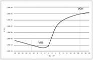
图6为本申请实施例提供的液晶手写板中薄膜晶体管在源极电压为20V时的转移特性曲线;6 is a transfer characteristic curve of a thin film transistor in a liquid crystal tablet provided by an embodiment of the present application when the source voltage is 20V;
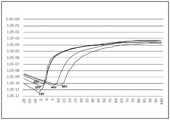
图7为本申请实施例提供的液晶手写板中薄膜晶体管在不同源极电压下的转移特性曲线;7 is a transfer characteristic curve of a thin film transistor in a liquid crystal tablet provided by an embodiment of the present application under different source voltages;
图8为本申请实施例提供的液晶手写板的控制方法的流程示意图。FIG. 8 is a schematic flowchart of a control method for a liquid crystal tablet provided by an embodiment of the present application.
图中:In the picture:
10-液晶手写板;11-液晶面板;12-驱动电路;110-双稳态液晶层;111-第一基板;112-第二基板;100-薄膜晶体管;101-栅极线;102-数据线;121-调节模块;122-驱动模块;123-检测装置;130-像素电极;131-公共电极;124-存储模块;10-liquid crystal tablet; 11-liquid crystal panel; 12-drive circuit; 110-bistable liquid crystal layer; 111-first substrate; 112-second substrate; 100-thin film transistor; 101-gate line; 102-data line; 121-adjustment module; 122-drive module; 123-detection device; 130-pixel electrode; 131-common electrode; 124-storage module;
1001-栅极;1002-有源层;1003-源漏极层;1004-第一绝缘层;1005-第二绝缘层;200-液晶分子;1110-第一衬底;1120-第二衬底;1001-gate; 1002-active layer; 1003-source and drain layer; 1004-first insulating layer; 1005-second insulating layer; 200-liquid crystal molecule; 1110-first substrate; 1120-second substrate ;
21-擦除区;22-非擦除区。21-erased area; 22-non-erased area.
具体实施方式Detailed ways
下面详细描述本申请,本申请的实施例的示例在附图中示出,其中自始至终相同或类似的标号表示相同或类似的部件或具有相同或类似功能的部件。此外,如果已知技术的详细描述对于示出的本申请的特征是不必要的,则将其省略。下面通过参考附图描述的实施例是示例性的,仅用于解释本申请,而不能解释为对本申请的限制。The application is described in detail below, and examples of embodiments of the application are illustrated in the accompanying drawings, wherein the same or similar reference numerals refer to the same or similar components or components having the same or similar functions throughout. Also, detailed descriptions of known technologies are omitted if they are not necessary for illustrating features of the present application. The embodiments described below with reference to the accompanying drawings are exemplary and are only used to explain the present application, but not to be construed as a limitation on the present application.
本技术领域技术人员可以理解,除非另外定义,这里使用的所有术语(包括技术术语和科学术语),具有与本申请所属领域中的普通技术人员的一般理解相同的意义。还应该理解的是,诸如通用字典中定义的那些术语,应该被理解为具有与现有技术的上下文中的意义一致的意义,并且除非像这里一样被特定定义,否则不会用理想化或过于正式的含义来解释。It will be understood by those skilled in the art that, unless otherwise defined, all terms (including technical and scientific terms) used herein have the same meaning as commonly understood by one of ordinary skill in the art to which this application belongs. It should also be understood that terms, such as those defined in a general dictionary, should be understood to have meanings consistent with their meanings in the context of the prior art and, unless specifically defined as herein, should not be interpreted in idealistic or overly formal meaning to explain.
本技术领域技术人员可以理解,除非特意声明,这里使用的单数形式“一”、“一个”、“所述”和“该”也可包括复数形式。应该进一步理解的是,本申请的说明书中使用的措辞“包括”是指存在所述特征、整数、步骤、操作、元件和/或组件,但是并不排除存在或添加一个或多个其他特征、整数、步骤、操作、元件、组件和/或它们的组。应该理解,当我们称元件被“连接”或“耦接”到另一元件时,它可以直接连接或耦接到其他元件,或者也可以存在中间元件。此外,这里使用的“连接”或“耦接”可以包括无线连接或无线耦接。这里使用的措辞“和/或”包括一个或更多个相关联的列出项的全部或任一单元和全部组合。It will be understood by those skilled in the art that the singular forms "a", "an", "the" and "the" as used herein can include the plural forms as well, unless expressly stated otherwise. It should be further understood that the word "comprising" used in the specification of this application refers to the presence of stated features, integers, steps, operations, elements and/or components, but does not preclude the presence or addition of one or more other features, Integers, steps, operations, elements, components and/or groups thereof. It will be understood that when we refer to an element as being "connected" or "coupled" to another element, it can be directly connected or coupled to the other element or intervening elements may also be present. Furthermore, "connected" or "coupled" as used herein may include wirelessly connected or wirelessly coupled. As used herein, the term "and/or" includes all or any element and all combination of one or more of the associated listed items.
液晶手写板作为液晶手写板的一种,具有功耗低且笔迹清晰的优势,近年来占据了较多的市场份额。液晶手写板通常包括相对设置的两个基板,以及位于两个基板之间的双稳态液晶层,双稳态液晶层中包括双稳态液晶分子。双稳态液晶分子具有平面织构状态(Planar Texture;简称:P态)、焦锥织构状态(Focal Conic Texture;简称:FC态)和垂直织构状态(Hometropic Texture;简称:H态)。其中,P态和FC态是稳定状态,无需电压即可保持,H态为不稳定状态,在持续发送电压时呈现。As a kind of liquid crystal tablet, the LCD tablet has the advantages of low power consumption and clear handwriting, and has occupied more market shares in recent years. A liquid crystal tablet generally includes two substrates disposed opposite to each other, and a bistable liquid crystal layer located between the two substrates, and the bistable liquid crystal layer includes bistable liquid crystal molecules. Bistable liquid crystal molecules have a planar texture state (Planar Texture; abbreviated: P state), a focal conic texture state (Focal Conic Texture; abbreviated: FC state) and a hometropic texture state (Hometropic Texture; abbreviated: H state). Among them, the P state and the FC state are stable states that can be maintained without a voltage, and the H state is an unstable state that appears when a voltage is continuously sent.
当液晶手写板受到外部压力时,双稳态液晶层中的双稳态液晶分子在外部压力作用下翻转为P态,可以反射可见光,液晶手写板受到外部压力的区域显示书写的笔迹;需要擦除笔迹时,控制擦除区内的薄膜晶体管开启并对薄膜晶体管发送源极电压,以对擦除区内的像素电极进行充电,使擦除区内的像素电极与公共电极之间形成电压差,因此位于擦除区的双稳态液晶分子在该电压差的作用下,重新排列为FC态,不反射可见光,擦除区内书写的笔迹可被擦除;同时控制非擦除区内的像素电极不充电,非擦除区内的笔迹不发生变化,由此可实现液晶手写板的局部擦除。When the liquid crystal tablet is subjected to external pressure, the bistable liquid crystal molecules in the bistable liquid crystal layer are turned to P state under the action of external pressure, which can reflect visible light, and the area of the liquid crystal tablet subjected to external pressure displays the written handwriting; need to wipe When removing handwriting, control the thin film transistor in the erasing area to turn on and send the source voltage to the thin film transistor to charge the pixel electrode in the erasing area, so that a voltage difference is formed between the pixel electrode and the common electrode in the erasing area , so the bistable liquid crystal molecules located in the erasing area are rearranged to the FC state under the action of the voltage difference, do not reflect visible light, and the handwriting written in the erasing area can be erased; The pixel electrode is not charged, and the handwriting in the non-erasing area does not change, thereby realizing partial erasing of the liquid crystal tablet.
具体的,请参阅图1、图2和图4,对擦除区21所对应的薄膜晶体管100发送源极电压(与擦除区21内的薄膜晶体管100所处同一列的薄膜晶体管100也同样被施加了源极电压,位于其他列的薄膜晶体管100上不加载源极电压),同时通过栅极线101对擦除区21内的薄膜晶体管100发送栅极开启电压(与擦除区21内的薄膜晶体管100所处同一行的薄膜晶体管100也同样被施加了栅极开启电压),通过栅极线101对与擦除区21内的薄膜晶体管100不同行的薄膜晶体管100(即图4中的目标区,目标区为非擦除区所包括的区域)施加栅极关断电压。被同时施加了栅极开启电压和源极电压的薄膜晶体管100(即图4中擦除区内的薄膜晶体管100)开启,擦除区21内的像素电极130被充电,擦除区21内的像素电极130与公共电极之间形成电压差,位于擦除区21内的双稳态液晶分子在该电压差的作用下重新翻转为FC态,擦除区21内书写的笔迹可被擦除。非擦除区22内的薄膜晶体管100处于关断状态,非擦除区22内的像素电极130不充电,非擦除区22内的笔迹不发生变化。Specifically, please refer to FIG. 1 , FIG. 2 and FIG. 4 , the source voltage is sent to the
本申请的发明人考虑到,由于随着使用时间的增加液晶分子会变得难以发生翻转,因此需要使像素电极和公共电极之间形成更大的电压差,即需要给薄膜晶体管发送更大的源极电压。然而,随着源极电压的增大,薄膜晶体管的转移特性曲线会发生偏移,使薄膜晶体管关断的栅极关断电压也会发生变化(一般认为薄膜晶体管的漏电流在小于10-10A时处于关断状态)。结合图1和图2和图4所示,当源极电压增大时,若发送给非擦除区22中的第一子目标区和第二子目标区的薄膜晶体管100的栅极关断电压保持不变,第一子目标区和第二子目标区可以作为目标区,会造成非擦除区22中的第二子目标区的薄膜晶体管100(图4中与擦除区21内的薄膜晶体管100位于同一列的薄膜晶体管100)无法完全关断,第二子目标区内的像素电极会被充电,导致位于第二子目标区的双稳态液晶分子发生偏转,在宏观上表现为非擦除区内的笔迹也被擦除,即出现了误擦除现象,这对于液晶手写板的使用造成了影响。The inventors of the present application have considered that since the liquid crystal molecules will become difficult to flip as the usage time increases, a larger voltage difference needs to be formed between the pixel electrode and the common electrode, that is, a larger voltage difference needs to be sent to the thin film transistor. source voltage. However, as the source voltage increases, the transfer characteristic curve of the thin film transistor will shift, and the gate turn-off voltage that turns the thin film transistor off will also change (it is generally considered that the leakage current of the thin film transistor is less than10-10 A is in the off state). 1, 2 and 4, when the source voltage increases, if the gates of the
本申请提供的液晶手写板及其控制方法,旨在解决现有技术的如上技术问题。The liquid crystal tablet and the control method thereof provided by the present application aim to solve the above technical problems in the prior art.
下面结合附图详细介绍一下本申请实施例提供的液晶手写板及其控制方法。The liquid crystal tablet and the control method thereof provided by the embodiments of the present application will be described in detail below with reference to the accompanying drawings.
首先,本申请实施例提供了一种液晶手写板10,如图3和图4所示,包括互相电连接的液晶面板11和驱动电路12;First, an embodiment of the present application provides a
液晶面板11包括相对设置的第一基板111和第二基板112,以及设置在第一基板111和第二基板112之间的双稳态液晶层110,第一基板111包括若干阵列设置的薄膜晶体管100;The
驱动电路12被配置为当液晶手写板10需要对擦除区21进行擦除时,确定栅极开启电压和栅极关断电压;The driving
将栅极开启电压发送给擦除区21内的薄膜晶体管100,将栅极关断电压发送给目标区内的薄膜晶体管100,目标区为非擦除区22包括的区域,且目标区内的薄膜晶体管100与擦除区内21的薄膜晶体管100连接不同的栅极线101,以执行对液晶手写板10擦除区21的擦除操作;The gate turn-on voltage is sent to the
其中,栅极关断电压的大小可调节,使液晶手写板10的目标区的薄膜晶体管100在接收到栅极关断电压时保持关断状态。The magnitude of the gate-off voltage can be adjusted, so that the
具体的,结合图3、图4和图5所示,液晶手写板10包括相对设置的第一基板111和第二基板112,以及设置在第一基板111和第二基板112之间的双稳态液晶层110,第一基板111包括若干阵列设置的薄膜晶体管100和像素电极130,薄膜晶体管100包括栅极1001、有源层1002和源漏极1003,源漏极1003与数据线102电连接,栅极1001与栅极线101电连接,栅极1001与有源层1002之间设有第一绝缘层1004,像素电极130与源漏极1003之间设有第二绝缘层1005。栅极线101沿图4中第一方向延伸,数据线102沿图4中第二方向延伸,第一方向和第二方向交叉。薄膜晶体管100的源漏极1003和像素电极130电连接,第二基板112包括公共电极131。双稳态液晶层110中包括双稳态液晶分子,像素电极130与公共电极131之间存在电压差时,双稳态液晶分子在电场力的作用下发生偏转。当液晶手写板10受到外部压力时,双稳态液晶分子翻转为P态,可以反射可见光,液晶手写板10上受到外力按压的区域显示书写的笔迹。可选的,请参阅图5,第二基板112为柔性基板,即第二衬底1120采用柔性材料,因此施加外部压力时更容易使力传到至双稳态液晶层110,有利于提高液晶手写板10的书写效果。Specifically, as shown in FIG. 3 , FIG. 4 and FIG. 5 , the
结合图3和图4所示,当需要擦除笔迹时,驱动电路12中的源极驱动电路(图3中未示出)通过数据线102对擦除区21所对应的薄膜晶体管100发送源极电压(与擦除区21内的薄膜晶体管100所处同一列的薄膜晶体管100也同样被施加了源极电压,位于其他列的薄膜晶体管100上不加载源极电压),同时通过栅极线101对擦除区21内的薄膜晶体管100发送栅极开启电压(与擦除区21内的薄膜晶体管100所处同一行的薄膜晶体管100也同样被施加了栅极开启电压),通过栅极线101对与擦除区21内的薄膜晶体管100不同行的薄膜晶体管100(即图4中第一子目标区和第二子目标区内的薄膜晶体管)施加栅极关断电压。被施加了栅极开启电压和源极电压的薄膜晶体管100(即图4中擦除区内的薄膜晶体管100)开启,擦除区21内的像素电极130被充电,擦除区21内的像素电极130与公共电极之间形成电压差,位于擦除区21内的双稳态液晶分子在该电压差的作用下重新翻转为FC态,擦除区21内书写的笔迹可被擦除。非擦除区22内的薄膜晶体管100处于关断状态,非擦除区22内的像素电极130不充电,非擦除区22内的笔迹不发生变化。As shown in FIG. 3 and FIG. 4 , when the handwriting needs to be erased, the source driver circuit (not shown in FIG. 3 ) in the
需要说明的是,可通过薄膜晶体管100的输出电流(薄膜晶体管100的漏极电流)的大小来判断薄膜晶体管100是否完全关断,通常当薄膜晶体管100的输出电流小于10-10A时,认为薄膜晶体管100处于完全关断状态,否则认为薄膜晶体管100开启。It should be noted that whether the
需要说明的是,如图4所示,本申请实施例中的非擦除区22包括第一子目标区、第二子目标区和第三子目标区,本申请实施例中将栅极关断电压发送给目标区内的薄膜晶体管,指将栅极关断电压发送给第二子目标区内的薄膜晶体管,第三子目标区内的薄膜晶体管由于与擦除区21内的薄膜晶体管位于同一行,因此,第三子目标区内的薄膜晶体管接收到的为栅极开启电压,由于并不对第三子目标区内的薄膜晶体管施加源极电压,因此,第三子目标区内的薄膜晶体管也处于关断状态,即并不对第三子目标区内的薄膜晶体管进行充电;同样地,也不对第一子目标区内的薄膜晶体管施加源极电压,因此,第一子目标区内的薄膜晶体管也处于关断状态,即也不对第一子目标区内的薄膜晶体管进行充电。实际上,由于在擦除过程中,仅对第二子目标区内的薄膜晶体管施加源极电压,因此,只要确保第二子目标区内的薄膜晶体管完全关断即可。It should be noted that, as shown in FIG. 4 , the
需要说明的是,本申请实施例中,在将栅极关断电压发送给目标区内的薄膜晶体管前,需要对确定的栅极关断电压(可以认为是初始栅极关断电压)进行判断,若判断第二子目标区存在误擦除时(具体判断方法将在下面进行详细描述),则对确定的栅极关断电压进行调节(即对初始栅极关断电压进行调节),将调节后的栅极关断电压发送给目标区内的薄膜晶体管;若判断第二子目标区不存在误擦除时,则直接将确定的栅极关断电压发送给目标区内的薄膜晶体管(即将初始栅极关断电压发送给目标区内的薄膜晶体管)。It should be noted that, in the embodiment of the present application, before sending the gate-off voltage to the thin film transistor in the target area, the determined gate-off voltage (which can be considered as the initial gate-off voltage) needs to be judged , if it is judged that there is erroneous erasing in the second sub-target area (the specific judgment method will be described in detail below), then the determined gate turn-off voltage is adjusted (that is, the initial gate turn-off voltage is adjusted), and the The adjusted gate turn-off voltage is sent to the thin film transistor in the target area; if it is judged that there is no false erasure in the second sub-target area, the determined gate turn-off voltage is directly sent to the thin film transistor in the target area ( That is, the initial gate-off voltage is sent to the thin-film transistors in the target area).
在本申请的实施例中,如图3所示,驱动电路12包括调节模块121,调节模块121被配置为对栅极关断电压的大小进行调节,和/或,调节模块121被配置为对栅极开启电压的大小进行调节。具体的,在液晶手写板10的使用过程中,首先判断第二子目标区是否存在误擦除,若存在误擦除,则通过调节模块121对栅极关断电压的大小进行调节;具体实施时,判断第二子目标区是否存在误擦除,包括:使用者通过擦除状态的观察,判断第二子目标区是否存在误擦除,进而对栅极关断电压进行手动调节。In the embodiment of the present application, as shown in FIG. 3 , the driving
请参阅图4,在对液晶手写板10上的字迹进行擦除时,若发现需要保留字迹的区域(需要避免擦除的区域,即图4中的第二子目标区)的字迹出现了变淡的情况,说明此时第二子目标区内的薄膜晶体管100的特性已发生了偏移,驱动模块122发送至第二子目标区内的薄膜晶体管100的栅极关断电压不能使薄膜晶体管100完全关断。此时使用者可对栅极关断电压进行手动调整,以使第二子目标区内的薄膜晶体管100能够完全关断,避免出现误擦除现象。具体的,调节模块121可以为设置在液晶手写板10中的旋钮,该旋钮可以对应多个调节档位,当使用者发现第二子目标区的字迹出现了变淡的情况,可以通过旋转该旋钮观察第二子目标区的字迹变化情况,当第二子目标区变淡的字迹恢复到与其它字迹相同时,停止旋转该旋钮,栅极关断电压调节完成,驱动模块122发送当前调节后的栅极关断电压给第二子目标区的薄膜晶体管,以使第二子目标区的薄膜晶体管关断;栅极关断电压的手动调节方式可根据实际情况进行确定。Please refer to FIG. 4 , when erasing the handwriting on the
需要说明的是,随着使用时间的增加,液晶手写板10中液晶分子的偏转变得困难,导致擦除区21的擦除效果不佳,因此需要增大发送至薄膜晶体管100的源极电压,使擦除区21内的液晶分子完全偏转。具体的,可通过观察擦除区21内的擦除状态手动增大源极电压,也可以按照特定的数值自动增大源极电压,例如根据液晶手写板10中的薄膜晶体管100特性(沟道长宽比等),初始的源极驱动电压设置为15v(保证薄膜晶体管100开启时漏电流达到一定要求),之后增大到20v,25v等。It should be noted that, with the increase of use time, the deflection of the liquid crystal molecules in the
请参阅图3,驱动电路还包括存储模块124,存储模块124被配置为预存栅极关断电压与源极电压的对应关系,和/或被配置为预存栅极开启电压与源极电压的对应关系;调节模块121被配置为根据存储模块124中预存的关断电压与源极电压的对应关系调节栅极关断电压,和/或调节模块121被配置为根据存储模块124中预存的开启电压与源极电压的对应关系调节栅极开启电压。具体实施时,存储模块124可以位于调节模块121内,也可以位于调节模块121外;位于调节模块121外时,通过与调节模块121连接,实现信号的传输。Referring to FIG. 3 , the driving circuit further includes a
具体的,在制作液晶手写板10之前,对液晶手写板10中准备采用的薄膜晶体管100进行测试。对薄膜晶体管100的源极发送一个固定电压,然后对薄膜晶体管100的栅极发送不同的电压,并测量薄膜晶体管100在不同的栅极电压下漏极电流的大小,将不同的栅极电压与漏极电流的数值记录下来,并绘制成曲线,即可得到薄膜晶体管100的转移特性曲线,如图6所示。同样地,改变薄膜晶体管100的源极电压,可以得到多个不同源极电压对应的薄膜晶体管100的转移特性曲线,如图7所示。根据转移特性曲线可得到栅极关断电压(VGL)、栅极开启电压(VGH)、源极电压以及输出电流的对应关系,将栅极关断电压与源极电压的对应关系预存至存储模块124中。薄膜晶体管100的输出电流(漏极电流)的大小与源极电压的大小以及薄膜晶体管100的自身结构特性(薄膜晶体管100的沟道长宽比)相关。在本申请的实施例中,薄膜晶体管100的沟道长宽比为50μm/4μm,通过测试所得到的转移特性曲线是针对沟道长宽比为50μm/4μm的薄膜晶体管。可以理解的是,实际应用中薄膜晶体管100的结构可根据具体情况进行确定。Specifically, before the
如图6所示,当源极电压为20V时,若要使薄膜晶体管100的输出电流小于10-10A,则需要使栅极关断电压在-11V至-2V,即栅极关断电压的最佳范围在-11V至-2V之间。具体的栅极关断电压的最佳范围可根据实际情况进行确定。As shown in FIG. 6 , when the source voltage is 20V, if the output current of the
可选的,在本申请的实施例中,如图3所示,液晶手写板10中还包括检测装置123,检测装置123被配置为在液晶手写板需要对擦除区进行擦除时,检测发送至目标区内的薄膜晶体管100的源极电压,并将源极电压发送给驱动模块122;驱动模块122根据检测装置123发送的当前源极电压以及栅极关断电压与源极电压的对应关系,判断是否需要对栅极关断电压调节;若需要进行调节,则对输出的栅极关断电压的大小进行调整。Optionally, in the embodiment of the present application, as shown in FIG. 3 , the
具体的,结合图3和图4所示,检测装置123与调节模块121互相电连接,在对液晶手写板10进行擦除时,检测装置123对发送给目标区22内薄膜晶体管100的源极电压进行实时检测,并将检测的结果发送至调节模块121;调节模块121被配置为根据检测装置123发送的当前源极电压、以及预存的栅极关断电压与源极电压的对应关系,将当前的栅极关断电压调整至预设数值范围内。当源极电压不同时,使薄膜晶体管100的输出电流小于10-10A的栅极关断电压的最佳范围也不同。如图7所示,当源极电压为20V时,若要使薄膜晶体管100的输出电流小于10-10A,则需要使栅极关断电压在-11V至-2V,即栅极关断电压的最佳范围在-11V至-2V之间。具体的栅极关断电压的最佳范围可根据实际情况进行确定。Specifically, as shown in FIG. 3 and FIG. 4 , the
请参阅图3和图4,在液晶手写板10进行擦除时,检测装置123对发送至目标区内薄膜晶体管100的源极电压进行实时检测,并将检测到的源极电压发送至调节模块121。调节模块121根据预存的栅极关断电压与源极电压的对应关系,确定与此时的源极电压所对应的栅极关断电压的最佳范围,并将当前的栅极关断电压调整至最佳范围内,并将调整后的栅极关断电压发送至驱动模块122,驱动模块122再将调节后的栅极关断电压发送至目标区内薄膜晶体管100,使目标区内薄膜晶体管100的输出电流小于10-10A,保证了非擦除区22内薄膜晶体管100的关断,避免了误擦除的发生。Please refer to FIG. 3 and FIG. 4 , when the
可选的,通过转移特性曲线可确定栅极关断电压的最佳数值,并将栅极关断电压调整至最佳数值,由此可以最大程度上的避免出现误擦除现象。如图7所示,当源极电压为20V时,栅极关断电压在-5V时输出电流最小,因此-5V即为栅极关断电压的最佳数值;如图7所示,当源极电压为30V时,栅极关断电压在-3V时输出电流最小,因此-3V即为栅极关断电压的最佳数值。栅极关断电压的最佳数值,可以根据实际情况进行确定。通过将栅极关断电压调节至最佳数值,可以使图4中子目标区内的薄膜晶体管的漏电流最小(即使非擦除区内的薄膜晶管完全关断),最大程度上的避免了误擦除现象的产生。下表1为不同源极电压下,薄膜晶体管100的输出电流最小时栅极关断电压的数值:表1中第一列表示擦除时,施加到擦除区的薄膜晶体管的源极电压,第二列表示第一子目标区和第二子目标区的薄膜晶体管的最小输出电流,第三列表示施加到第一子目标区和第二子目标区的薄膜晶体管的最佳的栅极关断电压。Optionally, the optimal value of the gate turn-off voltage can be determined through the transfer characteristic curve, and the gate turn-off voltage can be adjusted to the optimal value, so that the phenomenon of false erasing can be avoided to the greatest extent. As shown in Figure 7, when the source voltage is 20V, the output current is the smallest when the gate turn-off voltage is -5V, so -5V is the optimal value of the gate turn-off voltage; as shown in Figure 7, when the source When the pole voltage is 30V, the output current is the smallest when the gate turn-off voltage is -3V, so -3V is the optimal value of the gate turn-off voltage. The optimal value of the gate turn-off voltage can be determined according to the actual situation. By adjusting the gate turn-off voltage to an optimal value, the leakage current of the thin film transistors in the sub-target region in FIG. 4 can be minimized (even if the thin film transistors in the non-erased region are completely turned off), avoiding erroneous erasing phenomenon. Table 1 below shows the value of the gate turn-off voltage when the output current of the

表1Table 1
通过对源极电压实时检测,并根据检测结果实时调节栅极关断电压,可以使调节更加便利和智能,更利于避免出现误擦除现象。需要说明的是,图7中的薄膜晶体管100转移特性曲线仅包括了源极电压为15V、20V、30V、40V和50V这五种情况,实际使用过程中可以测试薄膜晶体管100在更多不同的源极电压下的转移特性曲线,并根据转移特性曲线将栅极关断电压与源极电压的对应关系预存至存储模块124中,由此可以使栅极关断电压的调节更加精确。By detecting the source voltage in real time, and adjusting the gate turn-off voltage in real time according to the detection result, the adjustment can be made more convenient and intelligent, and it is more beneficial to avoid the phenomenon of false erasing. It should be noted that the transfer characteristic curve of the
可选的,在本申请的实施例中,检测装置123被配置为在液晶手写板10需要对擦除区21进行擦除时,检测发送至擦除区21内的薄膜晶体管100的源极电压,并将源极电压发送给驱动模块122;驱动模块122根据检测装置123发送的当前源极电压以及栅极开启电压与源极电压的对应关系,判断是否需要对栅极开启电压进行调节,若需要进行调节,则对输出的栅极开启电压的大小进行调整。Optionally, in the embodiment of the present application, the detecting
具体的,在制作液晶手写板10之前,对液晶手写板10中准备采用的薄膜晶体管100进行测试。对薄膜晶体管100的源极发送一个固定电压,然后对薄膜晶体管100的栅极发送不同的电压,并测量薄膜晶体管100在不同的栅极电压下漏极电流的大小,将不同的栅极电压与漏极电流的数值记录下来,并绘制成曲线,即可得到薄膜晶体管100的转移特性曲线。薄膜晶体管100的漏极电流与源极电压以及薄膜晶体管100的自身结构特性(薄膜晶体管100的沟道长宽比)相关。通常认为,当薄膜晶体管100的漏极电流大于或者等于10-5A时,薄膜晶体管100的导通性能较好,即处于完全开启的状态。在本申请的实施例中,薄膜晶体管100的沟道长宽比为50μm/4μm,首先测量得到薄膜晶体管100在不同的源极电压下的转移特性曲线,从转移特性曲线中可得不同的源极电压下每条转移特性曲线中的输出电流和对应的栅极电压,即栅极关断电压与源极电压的对应关系,将栅极关断电压与源极电压的对应关系作为预设条件预存至存储模块124中。调节模块121被配置为根据栅极关断电压与源极电压的对应关系调节栅极开启电压的大小,驱动模块122发送调节后的栅极开启电压,以使擦除区21内的薄膜晶体管100开启,由此可以使擦除区21内的像素电极130能够被更好的充电,有利于改善擦除效果。Specifically, before the
可选的,在本申请的实施例中,液晶手写板10中包括检测装置123,检测装置123被配置为在液晶手写板10进行擦除时,实时检测发送至擦除区21内的薄膜晶体管100的源极电压,并将源极电压发送给调节模块121;存储模块124被配置为预存栅极开启电压与源极电压的对应关系,调节模块121被配置为根据检测装置123发送的当前源极电压和栅极开启电压与源极电压的对应关系,确定是否需要对当前的栅极开启电压进行调节,若需要进行调节,则确定调节后的栅极开启电压,并将调节后的栅极开启电压发送给驱动模块122。具体的,根据测试得到的薄膜晶体管100的转移特性曲线,可以确定使薄膜晶体管100的输出电流大于或者等于10-5A,所需要的栅极开启电压。例如,结合图6和图7所示,当源极电压为20V时,若要使薄膜晶体管100的输出电流大于10-5A,则需要使栅极开启电压大于15V。调节模块121将栅极开启电压的大小调整至15V以上后,驱动模块122发送调节后的栅极开启电压,以使擦除区21内的薄膜晶体管100的输出电流大于或者等于10-5A。Optionally, in the embodiment of the present application, the
通过实时检测发送至擦除区21薄膜晶体管100的源极电压,并根据栅极关断电压与源极电压的对应关系调节栅极开启电压的大小,可以使擦除区21内的薄膜晶体管100的输出电流足够大,由此使擦除区21内的像素电极130能够被更好的充电,有利于改善擦除效果。By detecting the source voltage sent to the
基于同一种发明构思,本申请实施例还提供了一种液晶手写板10的控制方法,如图8所示,包括:Based on the same inventive concept, an embodiment of the present application also provides a control method for the
S101、在液晶手写板需要对擦除区进行擦除时,对擦除区内的薄膜晶体管以及与擦除区内的薄膜晶体管连接同一条数据线的薄膜晶体管发送源极电压;S101, when the liquid crystal tablet needs to erase the erasing area, send the source voltage to the thin film transistors in the erasing area and the thin film transistors connected to the same data line with the thin film transistors in the erasing area;
S102、将栅极开启电压发送给擦除区内的薄膜晶体管,将栅极关断电压发送给目标区内的薄膜晶体管,目标区为非擦除区包括的区域,且目标区内的薄膜晶体管与擦除区内的薄膜晶体管连接不同的栅极线;其中,栅极关断电压的大小可调节,使目标区内的薄膜晶体管在接收到栅极关断电压时保持关断状态。S102, sending the gate turn-on voltage to the thin film transistors in the erasing area, and sending the gate off voltage to the thin film transistors in the target area, the target area is the area included in the non-erasing area, and the thin film transistors in the target area are Different gate lines are connected with the thin film transistors in the erasing area; wherein, the magnitude of the gate turn-off voltage can be adjusted, so that the thin film transistors in the target area keep the off state when receiving the gate turn-off voltage.
在本申请实施例提供的液晶手写板10的控制方法中,通过使驱动电路12所发送的栅极关断电压可调节,当源极电压增大导致使薄膜晶体管100能够完全关断的电压发生变化时,驱动电路12可以发送调节后的栅极关断电压至非擦除区22内的薄膜晶体管100,使非擦除区22内的薄膜晶体管100的输出电流小于10-10A,即保证非擦除区22内的薄膜晶体管100能够完全关断,由此避免了对非擦除区22内的像素电极130进行充电,防止出现误擦除现象。In the control method of the
可选的,在本申请的实施例中,液晶手写板10还包括检测装置123,将栅极关断电压发送给目标区内的薄膜晶体管,包括:Optionally, in the embodiment of the present application, the
检测发送至与擦除区内的薄膜晶体管连接同一条数据线的薄膜晶体管的源极电压;Detecting the source voltage sent to the thin film transistor connected to the same data line as the thin film transistor in the erasing area;
根据源极电压以及预存的源极电压和栅极关断电压的对应关系,确定是否需要对栅极关断电压进行调节,若需要进行调节,则对栅极关断电压进行调节后发送给目标区内的薄膜晶体管,否则直接将栅极关断电压发送给目标区内的薄膜晶体管。According to the source voltage and the corresponding relationship between the pre-stored source voltage and gate turn-off voltage, it is determined whether the gate turn-off voltage needs to be adjusted. If adjustment is required, the gate turn-off voltage is adjusted and sent to the target. Otherwise, the gate off voltage is directly sent to the thin film transistor in the target area.
结合图3和图4所示,当需要擦除笔迹时,驱动电路12中的源极驱动电路(图3中未示出)通过数据线102对擦除区21所对应的薄膜晶体管100发送源极电压(与擦除区21内的薄膜晶体管100所处同一列的薄膜晶体管100也同样被施加了源极电压,位于其他列的薄膜晶体管100上不加载源极电压),同时通过栅极线101对擦除区21内的薄膜晶体管100发送栅极开启电压(与擦除区21内的薄膜晶体管100所处同一行的薄膜晶体管100也同样被施加了栅极开启电压),通过栅极线101对与擦除区21内的薄膜晶体管100不处同一行的薄膜晶体管100(即图4中目标区内的薄膜晶体管)施加栅极关断电压。被施加了栅极开启电压和源极电压的薄膜晶体管100(即图4中擦除区内的薄膜晶体管100)开启,擦除区21内的像素电极130被充电,擦除区21内的像素电极130与公共电极之间形成电压差,位于擦除区21内的双稳态液晶分子在该电压差的作用下重新翻转为FC态,擦除区21内书写的笔迹可被擦除。非擦除区22内的薄膜晶体管100处于关断状态,非擦除区22内的像素电极130不充电,非擦除区22内的笔迹不发生变化。As shown in FIG. 3 and FIG. 4 , when the handwriting needs to be erased, the source driver circuit (not shown in FIG. 3 ) in the
在制作液晶手写板10之前,对液晶手写板10中准备采用的薄膜晶体管100进行测试。对薄膜晶体管100的源极发送一个固定电压,然后对薄膜晶体管100的栅极发送不同的电压,并测量薄膜晶体管100在不同的栅极电压下漏极电流的大小,将不同的栅极电压与漏极电流的数值记录下来,并绘制成曲线,即可得到薄膜晶体管100的转移特性曲线。薄膜晶体管100的漏极电流与源极电压以及薄膜晶体管100的自身结构特性(薄膜晶体管100的沟道长宽比)相关。在本申请的实施例中,薄膜晶体管100的沟道长宽比为50μm/4μm,请参阅图6和图7,通过测量得到薄膜晶体管100在不同的源极电压下的转移特性曲线,从转移特性曲线中可得不同的源极电压下每条转移特性曲线中的输出电流和对应的栅极电压,即栅极关断电压与源极电压的对应关系,将栅极关断电压与源极电压的对应关系作为预设条件预存至存储模块124中,栅源电压对应可以以类似于表1的形式预存在存储模块124中。Before manufacturing the
需要说明的是,图7中的薄膜晶体管100转移特性曲线仅包括了源极电压为15V、20V、30V、40V和50V这五种情况,实际使用过程中可以测试薄膜晶体管100在更多不同的源极电压下的转移特性曲线,并根据转移特性曲线将栅极关断电压与源极电压的对应关系预存至存储模块124中,由此可以使栅极关断电压的调节更加精确。It should be noted that the transfer characteristic curve of the
检测装置123对发送至非擦除区22内的薄膜晶体管100的源极电压进行实时检测,并将所检测到的当前源极电压发送至调节模块121,调节模块121根据当前的源极电压以及预存的栅极关断电压与源极电压的对应关系,确定是否需要对当前的栅极关断电压进行调节,若需要进行调节,则确定调节后的栅极关断电压,并将调节后的栅极关断电压发送给子目标区内的薄膜晶体管100(目标区包括子目标区)。The
具体的,根据检测装置123发送的当前源极电压和预存的栅极关断电压与源极电压的对应关系,确定是否需要对当前的栅极关断电压进行调节,包括:Specifically, according to the current source voltage sent by the
根据当前源极电压和栅极关断电压与源极电压的对应关系,确定与发送给非擦除区22内的薄膜晶体管100的源极电压所对应的栅极关断电压的预设数值范围;According to the current source voltage and the corresponding relationship between the gate off voltage and the source voltage, determine the preset value range of the gate off voltage corresponding to the source voltage sent to the
将当前的栅极关断电压与预设数值范围进行对比;Compare the current gate turn-off voltage with the preset value range;
若栅极关断电压小于预设数值范围中的最小值,增大栅极关断电压,直至栅极关断电压的大小在预设数值范围内;If the gate turn-off voltage is less than the minimum value in the preset value range, increase the gate turn-off voltage until the gate turn-off voltage is within the preset value range;
若栅极关断电压大于预设数值范围中的最大值,减小栅极关断电压,直至栅极关断电压的大小在预设数值范围内。If the gate-off voltage is greater than the maximum value in the preset value range, reduce the gate-off voltage until the gate-off voltage is within the preset value range.
具体的,若检测装置123检测到发送至子目标区内的薄膜晶体管100的源极电压为20V,调节模块121根据源极电压以及预存的栅极关断电压与源极电压的对应关系,确定需要使薄膜晶体管100的输出电流小于10-10A时,栅极关断电压需要在-11V至-2V,即栅极关断电压的预设数值范围在-11V至-2V之间。调节模块122对当前的栅极关断电压与预存的栅极关断电压的预设范围进行比较,若当前的栅极关断电压小于-11V(即小于预设数值范围中的最小值),则增大调整栅极关断电压,直至栅极关断电压在-11V至-2V之间(预设数值范围内);若当前的栅极关断电压大于-2V(即大于预设数值范围中的最大值),则减小调整栅极关断电压,直至栅极关断电压在-11V至-2V之间(预设数值范围内)。Specifically, if the
可选的,在本申请的实施例中,对擦除区内的薄膜晶体管以及与擦除区内的薄膜晶体管连接同一条数据线的薄膜晶体管发送源极电压,包括:Optionally, in the embodiment of the present application, sending source voltages to the thin film transistors in the erasing area and the thin film transistors connected to the same data line as the thin film transistors in the erasing area includes:
根据预存的源极电压与源极电压的持续发送时间的对应关系,确定与当前的源极电压所对应的预设时间;Determine the preset time corresponding to the current source voltage according to the pre-stored correspondence between the source voltage and the continuous transmission time of the source voltage;
控制源极电压的持续发送时间,使持续发送时间为预设时间。Control the continuous transmission time of the source voltage, so that the continuous transmission time is a preset time.
可选的,在本申请的实施例中,驱动模块122还被配置预存源极电压的大小以及源极电压持续发送时间的对应关系;以及根据源极电压的大小控制源极电压的持续发送时间,使持续发送时间在预设时间范围内。具体的,源极电压的持续时间可以通过实际的擦除测试进行确定,对于沟道长宽比为50μm/4μm的薄膜晶体管100,当源极电压为20V时,源极电压(说明是高电平)的持续发送时间为200至300毫秒时擦除效果为理想(不会出现误擦除现象),当源极电压为40V时,源极电压(说明是高电平)的持续发送时间为50至100毫秒时擦除效果为理想。通过测试,得到不同的源极电压下擦除效果较为理想时的源极电压持续发送时间,并将不同的源极电压以及持续发送时间的数据(即源极电压和持续发送时间的对应关系)预存至存储模块124中。在液晶手写板10的使用过程中,根据源极电压的大小,确定与源极电压所对应的持续时间(预设时间范围),然后对薄膜晶体管100发送源极电压时使源极电压的持续时间在预设时间范围内,即按照预设时间范围发送源极电压。通过控制源极电压的持续发送时间,可以减少像素电极130的充电时间,因此即使非擦除区22域的薄膜晶体管100存在一定的漏电流,子目标区内的像素电极130也不会被充分充电,由此避免了子目标区内的液晶分子翻转,进一步地降低了出现误擦除的风险。Optionally, in the embodiment of the present application, the
可选的,在本申请的实施例中,液晶手写板还包括检测装置,将栅极开启电压发送给擦除区内的薄膜晶体管,包括:Optionally, in the embodiment of the present application, the liquid crystal tablet further includes a detection device that sends the gate turn-on voltage to the thin film transistor in the erasing area, including:
检测发送至擦除区内的薄膜晶体管的源极电压;detecting the source voltage sent to the thin film transistor in the erased region;
根据源极电压以及预存的栅极开启电压与源极电压的对应关系,确定是否需要对栅极开启电压进行调节,若需要进行调节,则对栅极开启电压调节后发送给擦除区内的薄膜晶体管,否则直接将栅极开启电压发送给所述擦除区内的薄膜晶体管。According to the source voltage and the corresponding relationship between the pre-stored gate turn-on voltage and the source voltage, it is determined whether the gate turn-on voltage needs to be adjusted. Otherwise, the gate turn-on voltage is directly sent to the thin film transistor in the erasing area.
具体的,在制作液晶手写板10之前,对液晶手写板10中准备采用的薄膜晶体管100进行测试。对薄膜晶体管100的源极发送一个固定电压,然后对薄膜晶体管100的栅极发送不同的电压,并测量薄膜晶体管100在不同的栅极电压下漏极电流的大小,将不同的栅极电压与漏极电流的数值记录下来,并绘制成曲线,即可得到薄膜晶体管100的转移特性曲线。薄膜晶体管100的漏极电流与源极电压以及薄膜晶体管100的自身结构特性(薄膜晶体管100的沟道长宽比)相关。在本申请的实施例中,薄膜晶体管100的沟道长宽比为50μm/4μm,如图6和图7所示,通过测量得到薄膜晶体管100在不同的源极电压下的转移特性曲线,从转移特性曲线中可得不同的源极电压下每条转移特性曲线中的输出电流和对应的栅极电压,即栅极关断电压与源极电压的对应关系,将栅极关断电压与源极电压的对应关系作为预设条件预存至存储模块124中。Specifically, before the
检测装置123还被配置为在液晶手写板进行擦除时实时检测发送至擦除区21薄膜晶体管100的源极电压,并根据栅极关断电压与源极电压的对应关系调节栅极开启电压的大小。具体的,根据测试得到的薄膜晶体管100的转移特性曲线,可以确定使薄膜晶体管100的输出电流大于或者等于10-5A,所需要的栅极开启电压。例如,如图7所示,当源极电压为20V时,若要使薄膜晶体管100的输出电流大于10-5A,则需要使栅极开启电压大于15V。调节模块121将栅极开启电压的大小调整至15V以上后,驱动模块122发送调节后的栅极开启电压,以使擦除区21内的薄膜晶体管100的输出电流大于或者等于10-5A。如图7所示,当源极电压为40V时,若要使薄膜晶体管100的输出电流大于10-5A,则需要使栅极开启电压大于25V。调节模块121将栅极开启电压的大小调整至15V以上后,驱动模块122发送调节后的栅极开启电压,以使擦除区21内的薄膜晶体管100的输出电流大于或者等于10-5A。The
通过实时检测发送至擦除区21薄膜晶体管100的源极电压,并根据栅极开启电压与源极电压的对应关系调节栅极开启电压的大小,可以使擦除区21内的薄膜晶体管100的输出电流足够大,由此使擦除区21内的像素电极130能够被更好的充电,有利于改善擦除效果。By detecting the source voltage of the
应用本申请实施例,至少能够实现如下有益效果:By applying the embodiments of the present application, at least the following beneficial effects can be achieved:
1.本申请实施例提供的液晶手写板10包括第一基板111、第二基板112和双稳态液晶层110,第一基板111包括若干薄膜晶体管100;当液晶手写板10需要对擦除区21进行擦除时,驱动电路12被配置为确定栅极开启电压和栅极关断电压,对擦除区21内的薄膜晶体管100发送栅极开启电压,对目标区内的薄膜晶体管100发送栅极关断电压,目标区为非擦除区22包括的区域,且目标区内的薄膜晶体管100与擦除区21内的薄膜晶体管100连接不同的栅极线101,其中,栅极关断电压的大小可调节,使液晶手写板10的目标区的薄膜晶体管100在接收到栅极关断电压时保持关断状态。由此保证目标区内的薄膜晶体管100能够完全关断,避免了对非擦除区内的像素电极130进行充电,防止出现误擦除现象。1. The
2.在本申请的实施例中,设置检测装置123实时检测源极电压,并将测试得到栅源电压的对应关系作为预设条件预存至存储模块124中,通过对源极电压实时检测,并根据检测到的源极电压和预存的栅极关断电压与源极电压的对应关系调节栅极关断电压,可以使调节更加便利和智能,更利于避免出现误擦除现象。2. In the embodiment of the present application, the
3.通过对源极电压进行检测,确定与源极电压所对应的持续时间(预设时间范围),然后对薄膜晶体管100发送源极电压时使源极电压的持续时间在预设时间范围内,即按照预设时间范围发送源极电压。通过控制源极电压的持续发送时间,可以减少像素电极130的充电时间,因此即使非擦除区22域的薄膜晶体管100存在一定的漏电流,非擦除区22域的像素电极130也不会被充分充电,由此避免了非擦除区22域的液晶分子翻转,进一步地降低了出现误擦除的风险。3. Determine the duration (preset time range) corresponding to the source voltage by detecting the source voltage, and then send the source voltage to the
4.在本申请的实施例中,通过实时检测发送至擦除区21薄膜晶体管100的源极电压,并根据栅极关断电压与源极电压的对应关系调节栅极开启电压的大小,可以使擦除区21内的薄膜晶体管100的输出电流足够大,由此使擦除区21内的像素电极130能够被更好的充电,有利于改善擦除效果。4. In the embodiment of the present application, by detecting the source voltage of the
本技术领域技术人员可以理解,本申请中已经讨论过的各种操作、方法、流程中的步骤、措施、方案可以被交替、更改、组合或删除。进一步地,具有本申请中已经讨论过的各种操作、方法、流程中的其他步骤、措施、方案也可以被交替、更改、重排、分解、组合或删除。进一步地,现有技术中的具有与本申请中公开的各种操作、方法、流程中的步骤、措施、方案也可以被交替、更改、重排、分解、组合或删除。Those skilled in the art can understand that various operations, methods, steps, measures, and solutions in the process discussed in this application may be alternated, modified, combined or deleted. Further, other steps, measures, and solutions in the various operations, methods, and processes that have been discussed in this application may also be alternated, modified, rearranged, decomposed, combined, or deleted. Further, steps, measures and solutions in the prior art with various operations, methods, and processes disclosed in this application may also be alternated, modified, rearranged, decomposed, combined or deleted.
在本申请的描述中,需要理解的是,术语“中心”、“上”、“下”、“前”、“后”、“左”、“右”、“竖直”、“水平”、“顶”、“底”、“内”、“外”等指示的方位或位置关系为基于附图所示的方位或位置关系,仅是为了便于描述本申请和简化描述,而不是指示或暗示所指的装置或元件必须具有特定的方位、以特定的方位构造和操作,因此不能理解为对本申请的限制。In the description of this application, it should be understood that the terms "center", "upper", "lower", "front", "rear", "left", "right", "vertical", "horizontal", The orientation or positional relationship indicated by "top", "bottom", "inner", "outer", etc. is based on the orientation or positional relationship shown in the drawings, and is only for the convenience of describing the present application and simplifying the description, rather than indicating or implying The device or element referred to must have a particular orientation, be constructed and operate in a particular orientation, and therefore should not be construed as a limitation of the present application.
术语“第一”、“第二”仅用于描述目的,而不能理解为指示或暗示相对重要性或者隐含指明所指示的技术特征的数量。由此,限定有“第一”、“第二”的特征可以明示或者隐含地包括一个或者更多个该特征。在本申请的描述中,除非另有说明,“多个”的含义是两个或两个以上。The terms "first" and "second" are only used for descriptive purposes, and should not be construed as indicating or implying relative importance or implicitly indicating the number of technical features indicated. Thus, a feature defined as "first" or "second" may expressly or implicitly include one or more of that feature. In the description of this application, unless stated otherwise, "plurality" means two or more.
在本申请的描述中,需要说明的是,除非另有明确的规定和限定,术语“安装”、“相连”、“连接”应做广义理解,例如,可以是固定连接,也可以是可拆卸连接,或一体地连接;可以是直接相连,也可以通过中间媒介间接相连,可以是两个元件内部的连通。对于本领域的普通技术人员而言,可以具体情况理解上述术语在本申请中的具体含义。In the description of this application, it should be noted that, unless otherwise expressly specified and limited, the terms "installed", "connected" and "connected" should be understood in a broad sense, for example, it may be a fixed connection or a detachable connection Connection, or integral connection; it can be directly connected, or indirectly connected through an intermediate medium, and it can be the internal communication of two elements. For those of ordinary skill in the art, the specific meanings of the above terms in this application can be understood in specific situations.
在本说明书的描述中,具体特征、结构、材料或者特点可以在任何的一个或多个实施例或示例中以合适的方式结合。In the description of this specification, the particular features, structures, materials or characteristics may be combined in any suitable manner in any one or more embodiments or examples.
应该理解的是,虽然附图的流程图中的各个步骤按照箭头的指示依次显示,但是这些步骤并不是必然按照箭头指示的顺序依次执行。除非本文中有明确的说明,这些步骤的执行并没有严格的顺序限制,其可以以其他的顺序执行。而且,附图的流程图中的至少一部分步骤可以包括多个子步骤或者多个阶段,这些子步骤或者阶段并不必然是在同一时刻执行完成,而是可以在不同的时刻执行,其执行顺序也不必然是依次进行,而是可以与其他步骤或者其他步骤的子步骤或者阶段的至少一部分轮流或者交替地执行。It should be understood that although the various steps in the flowchart of the accompanying drawings are sequentially shown in the order indicated by the arrows, these steps are not necessarily executed in sequence in the order indicated by the arrows. Unless explicitly stated herein, the execution of these steps is not strictly limited to the order and may be performed in other orders. Moreover, at least a part of the steps in the flowchart of the accompanying drawings may include multiple sub-steps or multiple stages, and these sub-steps or stages are not necessarily executed at the same moment, but may be executed at different timings, and the execution sequence is also It does not have to be performed sequentially, but may be performed alternately or alternately with other steps or at least a portion of sub-steps or stages of other steps.
以上所述仅是本申请的部分实施方式,应当指出,对于本技术领域的普通技术人员来说,在不脱离本申请原理的前提下,还可以做出若干改进和润饰,这些改进和润饰也应视为本申请的保护范围。The above are only part of the embodiments of the present application. It should be pointed out that for those skilled in the art, without departing from the principles of the present application, several improvements and modifications can also be made. It should be regarded as the protection scope of this application.
Claims (12)
Translated fromChinesePriority Applications (1)
| Application Number | Priority Date | Filing Date | Title |
|---|---|---|---|
| CN202210247920.8ACN114647120B (en) | 2022-03-14 | 2022-03-14 | Liquid crystal handwriting board and control method thereof |
Applications Claiming Priority (1)
| Application Number | Priority Date | Filing Date | Title |
|---|---|---|---|
| CN202210247920.8ACN114647120B (en) | 2022-03-14 | 2022-03-14 | Liquid crystal handwriting board and control method thereof |
Publications (2)
| Publication Number | Publication Date |
|---|---|
| CN114647120Atrue CN114647120A (en) | 2022-06-21 |
| CN114647120B CN114647120B (en) | 2023-10-17 |
Family
ID=81993731
Family Applications (1)
| Application Number | Title | Priority Date | Filing Date |
|---|---|---|---|
| CN202210247920.8AActiveCN114647120B (en) | 2022-03-14 | 2022-03-14 | Liquid crystal handwriting board and control method thereof |
Country Status (1)
| Country | Link |
|---|---|
| CN (1) | CN114647120B (en) |
Citations (5)
| Publication number | Priority date | Publication date | Assignee | Title |
|---|---|---|---|---|
| US5761127A (en)* | 1991-11-20 | 1998-06-02 | Fujitsu Limited | Flash-erasable semiconductor memory device having an improved reliability |
| KR20060058421A (en)* | 2004-11-25 | 2006-05-30 | 삼성전자주식회사 | LCD and its driving method |
| CN112327546A (en)* | 2020-11-18 | 2021-02-05 | 京东方科技集团股份有限公司 | Liquid crystal tablet, handwriting device and control method of handwriting device |
| CN113419388A (en)* | 2021-08-23 | 2021-09-21 | 山东蓝贝思特教装集团股份有限公司 | Liquid crystal writing device and method adaptive to ambient light |
| CN113990235A (en)* | 2021-10-29 | 2022-01-28 | 京东方科技集团股份有限公司 | Display driving circuit, display driving method and display device |
- 2022
- 2022-03-14CNCN202210247920.8Apatent/CN114647120B/enactiveActive
Patent Citations (5)
| Publication number | Priority date | Publication date | Assignee | Title |
|---|---|---|---|---|
| US5761127A (en)* | 1991-11-20 | 1998-06-02 | Fujitsu Limited | Flash-erasable semiconductor memory device having an improved reliability |
| KR20060058421A (en)* | 2004-11-25 | 2006-05-30 | 삼성전자주식회사 | LCD and its driving method |
| CN112327546A (en)* | 2020-11-18 | 2021-02-05 | 京东方科技集团股份有限公司 | Liquid crystal tablet, handwriting device and control method of handwriting device |
| CN113419388A (en)* | 2021-08-23 | 2021-09-21 | 山东蓝贝思特教装集团股份有限公司 | Liquid crystal writing device and method adaptive to ambient light |
| CN113990235A (en)* | 2021-10-29 | 2022-01-28 | 京东方科技集团股份有限公司 | Display driving circuit, display driving method and display device |
Also Published As
| Publication number | Publication date |
|---|---|
| CN114647120B (en) | 2023-10-17 |
Similar Documents
| Publication | Publication Date | Title |
|---|---|---|
| JP3163637B2 (en) | Driving method of liquid crystal display device | |
| US9653028B2 (en) | Pixel structure | |
| KR100372986B1 (en) | A method of driving a liquid crystal display device, and a liquid crystal display device | |
| US5949391A (en) | Liquid crystal display device and driving method therefor | |
| WO2017128560A1 (en) | Pixel driver circuit | |
| WO2016090698A1 (en) | Liquid crystal display panel and drive method thereof | |
| US20050219187A1 (en) | Driving method for a liquid crystal display | |
| KR19990007353A (en) | LCD Display | |
| CN100582881C (en) | Liquid crystal display device and method of driving the same | |
| TWM419123U (en) | Pixel structure with pre-charge function | |
| CN100480821C (en) | Liquid crystal display device and method of driving the same | |
| CN104503113A (en) | Liquid crystal display panel and display device | |
| CN107331363A (en) | A kind of array base palte, its driving method and display device | |
| JP2003202546A (en) | Method and apparatus for driving liquid crystal display device | |
| CN119418666B (en) | Polarity partition control module, display panel, drive module and display device | |
| CN113971941A (en) | Driving module for active matrix driving cholesteric liquid crystal display device and driving method thereof | |
| US7375706B2 (en) | Pixel structure of a liquid crystal display and driving method thereof | |
| CN114647120B (en) | Liquid crystal handwriting board and control method thereof | |
| US20050270282A1 (en) | Flat display panel driving method and flat display device | |
| WO2019037339A1 (en) | Liquid crystal display apparatus and drive method therefor | |
| US7714821B2 (en) | OCB mode LCD and method for driving the same | |
| CN107479289B (en) | Pixel structure and array substrate | |
| US20080024468A1 (en) | Pixel structure of liquid crystal display and driving method thereof | |
| JP2007256793A (en) | Liquid crystal display device | |
| US20210225300A1 (en) | Liquid crystal display and driving method thereof |
Legal Events
| Date | Code | Title | Description |
|---|---|---|---|
| PB01 | Publication | ||
| PB01 | Publication | ||
| SE01 | Entry into force of request for substantive examination | ||
| SE01 | Entry into force of request for substantive examination | ||
| GR01 | Patent grant | ||
| GR01 | Patent grant |