CN114631305A - Coil component for correcting hand trembling and camera module having the same - Google Patents
Coil component for correcting hand trembling and camera module having the sameDownload PDFInfo
- Publication number
- CN114631305A CN114631305ACN202080072450.5ACN202080072450ACN114631305ACN 114631305 ACN114631305 ACN 114631305ACN 202080072450 ACN202080072450 ACN 202080072450ACN 114631305 ACN114631305 ACN 114631305A
- Authority
- CN
- China
- Prior art keywords
- electrode
- coil
- pattern
- electrodes
- line width
- Prior art date
- Legal status (The legal status is an assumption and is not a legal conclusion. Google has not performed a legal analysis and makes no representation as to the accuracy of the status listed.)
- Granted
Links
Images


Classifications
- H—ELECTRICITY
- H04—ELECTRIC COMMUNICATION TECHNIQUE
- H04N—PICTORIAL COMMUNICATION, e.g. TELEVISION
- H04N23/00—Cameras or camera modules comprising electronic image sensors; Control thereof
- H04N23/57—Mechanical or electrical details of cameras or camera modules specially adapted for being embedded in other devices
- G—PHYSICS
- G03—PHOTOGRAPHY; CINEMATOGRAPHY; ANALOGOUS TECHNIQUES USING WAVES OTHER THAN OPTICAL WAVES; ELECTROGRAPHY; HOLOGRAPHY
- G03B—APPARATUS OR ARRANGEMENTS FOR TAKING PHOTOGRAPHS OR FOR PROJECTING OR VIEWING THEM; APPARATUS OR ARRANGEMENTS EMPLOYING ANALOGOUS TECHNIQUES USING WAVES OTHER THAN OPTICAL WAVES; ACCESSORIES THEREFOR
- G03B5/00—Adjustment of optical system relative to image or object surface other than for focusing
- G03B5/06—Swinging lens about normal to the optical axis
- H—ELECTRICITY
- H01—ELECTRIC ELEMENTS
- H01F—MAGNETS; INDUCTANCES; TRANSFORMERS; SELECTION OF MATERIALS FOR THEIR MAGNETIC PROPERTIES
- H01F27/00—Details of transformers or inductances, in general
- H01F27/28—Coils; Windings; Conductive connections
- H01F27/29—Terminals; Tapping arrangements for signal inductances
- H—ELECTRICITY
- H04—ELECTRIC COMMUNICATION TECHNIQUE
- H04N—PICTORIAL COMMUNICATION, e.g. TELEVISION
- H04N23/00—Cameras or camera modules comprising electronic image sensors; Control thereof
- H04N23/50—Constructional details
- H04N23/54—Mounting of pick-up tubes, electronic image sensors, deviation or focusing coils
- H—ELECTRICITY
- H04—ELECTRIC COMMUNICATION TECHNIQUE
- H04N—PICTORIAL COMMUNICATION, e.g. TELEVISION
- H04N23/00—Cameras or camera modules comprising electronic image sensors; Control thereof
- H04N23/50—Constructional details
- H04N23/55—Optical parts specially adapted for electronic image sensors; Mounting thereof
- H—ELECTRICITY
- H04—ELECTRIC COMMUNICATION TECHNIQUE
- H04N—PICTORIAL COMMUNICATION, e.g. TELEVISION
- H04N23/00—Cameras or camera modules comprising electronic image sensors; Control thereof
- H04N23/60—Control of cameras or camera modules
- H04N23/68—Control of cameras or camera modules for stable pick-up of the scene, e.g. compensating for camera body vibrations
- H04N23/682—Vibration or motion blur correction
- H04N23/685—Vibration or motion blur correction performed by mechanical compensation
- H04N23/687—Vibration or motion blur correction performed by mechanical compensation by shifting the lens or sensor position
- G—PHYSICS
- G03—PHOTOGRAPHY; CINEMATOGRAPHY; ANALOGOUS TECHNIQUES USING WAVES OTHER THAN OPTICAL WAVES; ELECTROGRAPHY; HOLOGRAPHY
- G03B—APPARATUS OR ARRANGEMENTS FOR TAKING PHOTOGRAPHS OR FOR PROJECTING OR VIEWING THEM; APPARATUS OR ARRANGEMENTS EMPLOYING ANALOGOUS TECHNIQUES USING WAVES OTHER THAN OPTICAL WAVES; ACCESSORIES THEREFOR
- G03B2205/00—Adjustment of optical system relative to image or object surface other than for focusing
- G03B2205/0007—Movement of one or more optical elements for control of motion blur
- G03B2205/0023—Movement of one or more optical elements for control of motion blur by tilting or inclining one or more optical elements with respect to the optical axis
- G—PHYSICS
- G03—PHOTOGRAPHY; CINEMATOGRAPHY; ANALOGOUS TECHNIQUES USING WAVES OTHER THAN OPTICAL WAVES; ELECTROGRAPHY; HOLOGRAPHY
- G03B—APPARATUS OR ARRANGEMENTS FOR TAKING PHOTOGRAPHS OR FOR PROJECTING OR VIEWING THEM; APPARATUS OR ARRANGEMENTS EMPLOYING ANALOGOUS TECHNIQUES USING WAVES OTHER THAN OPTICAL WAVES; ACCESSORIES THEREFOR
- G03B2205/00—Adjustment of optical system relative to image or object surface other than for focusing
- G03B2205/0053—Driving means for the movement of one or more optical element
- G03B2205/0069—Driving means for the movement of one or more optical element using electromagnetic actuators, e.g. voice coils
Landscapes
- Engineering & Computer Science (AREA)
- Multimedia (AREA)
- Signal Processing (AREA)
- Physics & Mathematics (AREA)
- General Physics & Mathematics (AREA)
- Power Engineering (AREA)
- Coils Or Transformers For Communication (AREA)
- Studio Devices (AREA)
- Adjustment Of Camera Lenses (AREA)
Abstract
Description
Translated fromChinese技术领域technical field
实施例涉及一种用于校正手抖的线圈构件以及包括该线圈构件的摄像头模块。Embodiments relate to a coil member for correcting hand shake and a camera module including the coil member.
背景技术Background technique
随着各种类型的便携式终端的广泛分布和无线互联网服务的商业化,消费者关于便携式终端的要求也变得多样化。因此,将各种类型的附加装置安装在便携式终端中。With the wide distribution of various types of portable terminals and the commercialization of wireless Internet services, consumer demands for portable terminals have also diversified. Therefore, various types of additional devices are installed in portable terminals.
在各种类型的附加装置中,摄像头模块是代表性的示例,其可以拍摄对象的照片或视频,存储图像数据,并根据需要编辑和传输图像数据。Among various types of additional devices, a camera module is a representative example, which can take photos or videos of a subject, store image data, and edit and transmit the image data as needed.
近年来,在诸如笔记本式个人计算机、照相手机、PDA、智能装置、玩具等的各种多媒体领域,以及诸如监控摄像头和磁带录像机的信息终端的图像输入装置中,对紧凑型摄像头模块的使用需求不断增加。In recent years, there has been a demand for the use of compact camera modules in various multimedia fields such as notebook personal computers, camera phones, PDAs, smart devices, toys, etc., and image input devices of information terminals such as surveillance cameras and video tape recorders Increasing.
常规摄像头模块可以分为诸如固定焦点(F.F)型、自动聚焦(A.F)型以及光学图像稳定(OIS)型的摄像头模块。Conventional camera modules can be classified into camera modules such as a fixed focus (F.F) type, an auto focus (A.F) type, and an optical image stabilization (OIS) type.
另一方面,在OIS型的情况下,可以提供设置在电路板上的线圈图案等作为用于实现防抖功能的组件。此时,为了控制线圈图案中产生的电动势,应减小线圈图案的电阻。On the other hand, in the case of the OIS type, a coil pattern or the like provided on a circuit board may be provided as a component for realizing an anti-shake function. At this time, in order to control the electromotive force generated in the coil pattern, the resistance of the coil pattern should be reduced.
另一方面,线圈图案的电阻随着线圈长度的增大而增大,并且当线圈长度减小时,电阻减小,但是存在线圈图案中产生的电动势减小且特性变差的问题。On the other hand, the resistance of the coil pattern increases as the coil length increases, and when the coil length decreases, the resistance decreases, but there is a problem that the electromotive force generated in the coil pattern decreases and the characteristics deteriorate.
因此,需要在减小电阻的同时具有提高的特性的线圈图案和包括该线圈图案的摄像头模块。Therefore, there is a need for a coil pattern having improved characteristics while reducing resistance, and a camera module including the coil pattern.
发明内容SUMMARY OF THE INVENTION
技术问题technical problem
实施例提供了一种具有提高的特性的线圈图案以及包括该线圈图案的摄像头模块。Embodiments provide a coil pattern with improved characteristics and a camera module including the coil pattern.
技术方案Technical solutions
一种线圈构件,包括:基板,基板包括上表面和与上表面相对的下表面;第一线圈电极,第一线圈电极设置在基板的上表面上并且包括第一图案电极;以及第二线圈电极,第二线圈电极设置在基板的下表面上并且包括第二图案电极,第一线圈电极包括第一最外侧图案电极、第一最内侧图案电极以及第一最外侧图案电极和第一最内侧图案电极之间的第一中心图案电极,并且第一最外侧图案电极的线宽和第一最内侧图案电极的线宽中的至少一个大于第一中心图案电极的线宽。A coil member comprising: a substrate including an upper surface and a lower surface opposite to the upper surface; a first coil electrode provided on the upper surface of the substrate and including a first pattern electrode; and a second coil electrode , the second coil electrode is disposed on the lower surface of the substrate and includes a second pattern electrode, the first coil electrode includes a first outermost pattern electrode, a first innermost pattern electrode, and a first outermost pattern electrode and a first innermost pattern The first center pattern electrode between the electrodes, and at least one of the line width of the first outermost pattern electrode and the line width of the first innermost pattern electrode is larger than the line width of the first center pattern electrode.
有益效果beneficial effect
在根据实施例的线圈构件中,线圈电极的图案电极中的最外侧图案电极和/或最内侧图案电极的线宽可以与中心图案电极的线宽不同。In the coil member according to the embodiment, the line width of the outermost pattern electrode and/or the innermost pattern electrode among the pattern electrodes of the coil electrode may be different from the line width of the center pattern electrode.
详细地,线圈电极的图案电极中的最外侧图案电极和/或最内侧图案电极的线宽可以形成为大于中心图案电极的线宽。In detail, the line width of the outermost pattern electrode and/or the innermost pattern electrode among the pattern electrodes of the coil electrode may be formed to be larger than that of the center pattern electrode.
因此,通过增大使线圈电极的电阻改变的线圈电极的线宽,可以减小线圈电极的电阻。Therefore, by increasing the line width of the coil electrode which changes the resistance of the coil electrode, the resistance of the coil electrode can be reduced.
因此,通过减小线圈电极的电阻,可以提高线圈构件和包括该线圈构件的摄像头模块的特性。Therefore, by reducing the resistance of the coil electrode, the characteristics of the coil member and the camera module including the coil member can be improved.
此外,在根据实施例的线圈构件中,可以通过多个通路孔连接多个单元线圈电极。Furthermore, in the coil member according to the embodiment, a plurality of unit coil electrodes may be connected through a plurality of via holes.
因此,可以减小连接单元线圈电极的连接电极的长度和布置面积。因此,可以防止由于连接电极的长度增大而导致电阻增大。Therefore, the length and arrangement area of the connection electrodes of the connection unit coil electrodes can be reduced. Therefore, an increase in resistance due to an increase in the length of the connection electrode can be prevented.
此外,在根据实施例的线圈构件中,可以针对各个区域不同地形成线圈电极的图案电极之间的间距。Furthermore, in the coil member according to the embodiment, the spacing between the pattern electrodes of the coil electrode may be formed differently for each region.
详细地,在线圈构件中,线圈电极的弯曲区域中的图案电极之间的间距可以大于其他区域的图案电极之间的间距。In detail, in the coil member, the spacing between the pattern electrodes in the curved region of the coil electrode may be larger than the spacing between the pattern electrodes in other regions.
因此,在形成线圈电极时,可以增加感光图案的线宽,从而防止感光图案在弯曲区域中支撑较弱而塌陷。Therefore, when the coil electrodes are formed, the line width of the photosensitive pattern can be increased, thereby preventing the photosensitive pattern from being weakly supported and collapsing in the bending region.
也就是说,以精细线宽形成的感光图案可以形成为在弯曲区域中比在其他区域中大。因此,即使在弯曲区域中也可以稳定地形成感光图案。That is, a photosensitive pattern formed with a fine line width can be formed to be larger in the curved region than in other regions. Therefore, the photosensitive pattern can be stably formed even in the curved region.
因此,根据实施例的线圈构件可以防止线圈电极的短路和弯曲区域中的图案形状不均匀。因此,根据实施例的线圈构件可以具有提高的可靠性。Therefore, the coil member according to the embodiment can prevent the short circuit of the coil electrode and the unevenness of the pattern shape in the bent region. Therefore, the coil member according to the embodiment may have improved reliability.
此外,在根据实施例的线圈构件中,可以通过多个通路孔连接多个单元线圈电极。Furthermore, in the coil member according to the embodiment, a plurality of unit coil electrodes may be connected through a plurality of via holes.
因此,可以减小连接单元线圈电极的连接电极的长度和布置面积。因此,可以防止由于连接电极的长度增大而导致电阻增大,并且可以通过最小化布置面积来减小线圈构件的尺寸。Therefore, the length and arrangement area of the connection electrodes of the connection unit coil electrodes can be reduced. Therefore, the increase in resistance due to the increase in the length of the connection electrodes can be prevented, and the size of the coil member can be reduced by minimizing the arrangement area.
附图说明Description of drawings
图1是示出了根据一个实施例的摄像头模块的透视图的视图;1 is a view showing a perspective view of a camera module according to one embodiment;
图2是示出了根据该实施例的线圈构件的俯视图的视图;2 is a view showing a top view of the coil member according to the embodiment;
图3是示出了根据该实施例的线圈构件的仰视图的视图;3 is a view showing a bottom view of the coil member according to the embodiment;
图4和图5是用于说明根据一个实施例的线圈构件的线圈电极之间的连接关系的视图;4 and 5 are views for explaining a connection relationship between coil electrodes of a coil member according to an embodiment;
图6是示出了图2的一个区域的放大图的视图;6 is a view showing an enlarged view of a region of FIG. 2;
图7是示出了图6的区域A被放大的线圈图案的视图;FIG. 7 is a view showing an enlarged coil pattern of the area A of FIG. 6;
图8是示出了沿图6的区域B-B’截取的剖视图的视图;Fig. 8 is a view showing a cross-sectional view taken along the region B-B' of Fig. 6;
图9是示出了图3的一个区域的放大图的视图;FIG. 9 is a view showing an enlarged view of a region of FIG. 3;
图10是示出了图9的区域C被放大的线圈图案的视图;FIG. 10 is a view showing a coil pattern in which the region C of FIG. 9 is enlarged;
图11是示出了沿图9的区域D-D’截取的剖视图的视图;Fig. 11 is a view showing a cross-sectional view taken along the region D-D' of Fig. 9;
图12是示出了线圈电极形成在基板的两个表面上的线圈构件的剖视图的视图;12 is a view showing a cross-sectional view of a coil member in which coil electrodes are formed on both surfaces of a substrate;
图13是示出了用于说明另一个实施例的图2的一个区域的放大图的视图;13 is a view showing an enlarged view of a region of FIG. 2 for explaining another embodiment;
图14是示出了图13的一个区域被放大的线圈图案的视图;FIG. 14 is a view showing a coil pattern in which a region of FIG. 13 is enlarged;
图15是示出了沿图13的区域E-E’截取的剖视图的视图;Fig. 15 is a view showing a cross-sectional view taken along the region E-E' of Fig. 13;
图16是示出了沿图13的区域F-F’截取的剖视图的视图;Fig. 16 is a view showing a cross-sectional view taken along the region F-F' of Fig. 13;
图17是示出了用于说明另一个实施例的图3的一个区域的放大图的视图;17 is a view showing an enlarged view of a region of FIG. 3 for explaining another embodiment;
图18是示出了图17的一个区域被放大的线圈图案的视图;FIG. 18 is a view showing a coil pattern in which a region of FIG. 17 is enlarged;
图19是示出了沿图17的区域G-G’截取的剖视图的视图;Fig. 19 is a view showing a cross-sectional view taken along the region G-G' of Fig. 17;
图20是示出了图示图17的区域H-H’的剖视图的视图。Fig. 20 is a view showing a cross-sectional view illustrating a region H-H' of Fig. 17 .
具体实施方式Detailed ways
在下文中,将参考附图详细描述本公开的实施例。然而,本公开的精神和范围不限于所描述的实施例的一部分,并且可以以各种其他形式实现,并且在本公开的精神和范围内,可以选择性地结合和替换实施例的一个或多个元件。Hereinafter, embodiments of the present disclosure will be described in detail with reference to the accompanying drawings. However, the spirit and scope of the present disclosure is not limited to a portion of the described embodiments, and may be embodied in various other forms, and one or more of the embodiments may be selectively combined and substituted within the spirit and scope of the present disclosure a component.
此外,除非另有明确定义和描述,否则本公开的实施例中使用的术语(包括技术和科学术语)可以被解释为与本公开所属领域的技术人员通常理解的含义相同的含义,诸如在常用词典中定义的术语的术语可以被解释为具有与其在相关技术的上下文中的含义一致的含义。Also, unless explicitly defined and described otherwise, terms (including technical and scientific terms) used in the embodiments of the present disclosure may be construed as having the same meaning as commonly understood by one of ordinary skill in the art to which the present disclosure belongs, such as in commonly used Terms of terms defined in the dictionary may be interpreted as having meanings consistent with their meanings in the context of the related art.
此外,本公开的实施例中使用的术语用于描述实施例,并且不旨在限制本公开。在本说明书中,除非在措辞中明确说明,否则单数形式也可以包括复数形式,并且在描述为“A、B和C中的至少一个(或多个)”时,可以包括可以以A、B和C组合的所有组合中的至少一种。Also, the terms used in the embodiments of the present disclosure are used to describe the embodiments, and are not intended to limit the present disclosure. In this specification, unless the wording clearly dictates otherwise, the singular can also include the plural, and when described as "at least one (or more) of A, B, and C", can include the At least one of all combinations with C.
此外,在描述本公开的实施例的元件时,可以使用诸如第一、第二、A、B、(a)和(b)的术语。这些术语仅用于区分元件与其他元件,并且这些术语不限于元件的实质、顺序或次序。Also, terms such as first, second, A, B, (a), and (b) may be used when describing elements of embodiments of the present disclosure. These terms are only used to distinguish an element from other elements, and these terms are not limited to the substance, order, or sequence of the elements.
此外,当一个元件被描述为与其他元件“连接”、“耦合”或“连结”时,不仅可以包括该元件与其他元件直接“连接”、“耦合”或“连结”的情况,而且可以包括该元件通过该元件和该其他元件之间的另一个元件“连接”、“耦合”或“连结”的情况。Also, when an element is described as being "connected," "coupled," or "connected" to other elements, it can include not only instances where the element is directly "connected," "coupled," or "connected" to the other elements, but also includes A condition in which an element is "connected," "coupled," or "connected" by another element between the element and the other element.
此外,当描述为形成或设置在每个元件“上(上方)”或“下(下方)”时,“上(上方)”或“下(下方)”不仅可以包括两个元件彼此直接连接的情况,而且可以包括一个或多个其他元件形成或设置在两个元件之间的情况。Also, when described as being formed or disposed "on (above)" or "under (under)" each element, "over (above)" or "under (below)" may include not only two elements directly connected to each other case, and may include cases where one or more other elements are formed or disposed between two elements.
此外,当表述为“上(上方)”或“下(下方)”时,不仅可以包括基于一个元件的向上方向,而且可以包括基于一个元件的向下方向。Further, when expressed as "upper (upper)" or "lower (lower)", not only an upward direction based on one element but also a downward direction based on one element may be included.
图1是示出了根据一个实施例的摄像头模块的透视图的视图,并且图2是示出了根据该实施例的线圈构件的俯视图的视图。FIG. 1 is a view showing a perspective view of a camera module according to an embodiment, and FIG. 2 is a view showing a top view of a coil member according to the embodiment.
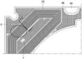
参考图1,根据本实施例的摄像头模块1000包括盖壳1100、第一动子1200、第二动子1300、定子1400、基座1500和弹性单元1600。此外,尽管在图1中未示出,但是根据本实施例的摄像头模块10可以进一步包括印刷电路板、IR滤光片、图像传感器等。1 , the
盖壳1100容纳弹性单元1600、第一动子1200、定子1400和第二动子1300,并且安装在基座1500上,以形成透镜驱动电机的外部。具体地,盖壳1100的内表面与基座1500的部分或全部侧表面紧密接触以安装在基座1500上,并且盖壳1100具有保护内部组件免受外部冲击和防止外部污染物渗透的功能。The
此外,盖壳1100还应执行保护透镜驱动电机或摄像头模块的组件免受移动电话等产生的外部无线电波干扰的功能。因此,盖壳1100优选地由金属材料形成。In addition, the
盖壳1100可以实现为将在下文描述的轭单元本身,或者可以通过在其内部模制轭单元来固定。此外,暴露透镜单元(未示出)的开口1110可以形成在盖壳1100的上表面上,并且在盖壳1100内弯曲的内轭(未示出)可以形成在盖壳1100的上表面的下端部分处。该内轭可以位于形成在线筒1210中的凹部1213中。在这种情况下,内轭可以设置在轭部的上表面上的开口周围的拐角处,或者可以设置在轭部的侧表面上,并且线筒的凹部可以形成在相应的位置处。The
此外,盖壳1100可以具有形成为在其下端部分的每个表面上延伸的至少一个紧固件1120,并且可以通过在基座1500中形成插入有紧固件1120的紧固槽1520来实现透镜驱动电机的更稳固的密封功能和紧固功能。此外,紧固件和紧固槽可以不单独存在,并且可以仅形成紧固件和紧固槽中的一个。In addition, the
同时,第一动子1200设置在透镜单元的侧表面上,以使透镜单元(未示出)移动。第一动子1200包括用于固定透镜单元的线筒1210和设置在线筒1210的外周表面上的第一线圈构件1220。Meanwhile, the
透镜单元(未示出)可以是设置有一个或多个透镜(未示出)的透镜镜筒,而实施例不限于此,并且可以包括能够支撑透镜的任意支架结构。The lens unit (not shown) may be a lens barrel provided with one or more lenses (not shown), but the embodiment is not limited thereto, and may include any support structure capable of supporting the lenses.
线筒1210的内周表面耦合到透镜单元的外周表面以固定透镜单元。此外,线筒1210外周表面上可以具有引导第一线圈构件1220的缠绕或安装的引导部1211。引导部1211可以与线筒1210的外表面一体地形成,并且可以沿线筒1210的外表面连续形成,或者可以形成为以预定间距间隔开。The inner peripheral surface of the
此外,弹簧紧固突出部1212可以形成在线筒1210的上表面和下表面上,其中,设置在基座1500的上侧以支撑线筒1210的上弹簧1710或下弹簧1720固定到弹簧紧固突出部1212。In addition,
此外,线筒1210可以进一步包括形成在其外周表面上的凹部1213,使得盖壳1100的内轭可以位于线筒1210与围绕线筒1210缠绕的第一线圈构件1220之间。In addition, the
此外,第一线圈构件1220可以由引导部1211引导并缠绕在线筒1210的外表面上,但是四个单独的线圈可以以90°间隔形成在线筒1210的外表面上。第一线圈构件1220可以接收从下文将要描述的印刷电路板(未示出)施加的电力以形成电磁场。Also, the
同时,第二动子1300可以放置为在第一动子1200的侧表面上面对第一动子1200,并且可以包括被设置为面对第一线圈构件1220的磁体部1310和固定磁体部1310的壳体1320。Meanwhile, the
具体地,磁体部1310可以通过粘合剂等安装在壳体1320上以设置在与第一线圈构件1220的外表面相对应的位置处,并且可以以相等的间距安装在壳体1320内部的四个拐角处以促进内部容积的有效利用。Specifically, the
壳体1320可以形成为与形成透镜驱动电机外部的盖壳1100的内表面相对应的形状。此外,考虑到生产率,壳体1320可以由绝缘材料形成,并且可以制造成注塑成型产品。壳体1320可以是用于OIS驱动的移动部件,并且可以设置为与盖壳1100间隔一定距离。The
在本实施例中,壳体1320可以形成为与盖壳1100的形状相对应并且与盖壳1100间隔预定距离的六面体形状,并且壳体1320的上下侧可以是开放的以支撑第一动子1200。此外,壳体1320可以包括在其侧表面上形成为与磁体部1310相对应的形状的磁体部紧固孔1311或磁体部紧固槽。In this embodiment, the
此外,可以形成至少两个限位部1312,其形成为从壳体1320的上表面以预定距离突出,以与盖壳1100的上表面接触,从而能够吸收外部冲击。限位部1312可以与壳体1320一体地形成。In addition, at least two
此外,弹簧紧固突出部1313可以形成在壳体1320的上表面和下表面上,设置在下文将要描述的基座1500的上侧以支撑壳体1320的上弹簧1710或下弹簧1720固定到弹簧紧固突出部1313。In addition,
同时,定子1400被放置为面对第二动子1300的下侧,以使第二动子1300移动,并且定子1400具有与形成在其中心的透镜单元相对应的通孔1411和1421。Meanwhile, the
具体地,定子1400可以包括第二线圈构件1410和基板,第二线圈构件1410被放置为面对磁体部1310的下侧,第二线圈构件1410设置在基板的上侧以施加电力,OIS芯片安装在基板上,并且基板可以是柔性印刷电路板1420。Specifically, the
第二线圈构件1410可以安装在设置在基座1500的上侧的印刷电路板1420上,或者形成在柔性印刷电路板或基板上,并且通孔1411形成在中心处,以使透镜单元(未示出)的光信号通过。同时,当考虑透镜驱动电机的微型化时,具体地,降低在作为光轴方向的z轴方向上的高度时,第二线圈构件1410可以形成为作为图案化线圈的精细图案(FP)线圈,并且设置在柔性印刷电路板上。The
在第二线圈单元1410的图案线圈中,可以控制图案线圈的线宽,以控制图案线圈的电动势。也就是说,通过增加图案线圈的线宽,可以减小图案线圈的电阻。下文将详细描述图案线圈。In the pattern coil of the
柔性印刷电路板1420可以设置在基座1500的上表面上,以向第二线圈构件1410施加电力,与第二线圈构件1410的通孔1411相对应的通孔1421形成在柔性印刷电路板1420上。此外,印刷电路板1420可以包括端子部1422,并且印刷电路板1420可以通过端子部1422供应有外部电力,其中,端子部1422的一端或彼此面对的两端弯曲以突出到基座1500的下侧。A flexible printed circuit board 1420 may be disposed on the upper surface of the base 1500 to apply power to the
此外,本实施例可以进一步包括霍尔传感器单元(未示出),该霍尔传感器单元安装在印刷电路板1420的下表面或上表面上,以与磁体部1310的位置相对应。In addition, the present embodiment may further include a hall sensor unit (not shown) mounted on the lower surface or the upper surface of the printed circuit board 1420 to correspond to the position of the
霍尔传感器单元感测被施加以用于检测磁体部1310的运动的电压和流过线圈的电流的强度和相位,并与提供的印刷电路板1420相互作用,以精确控制致动器。The hall sensor unit senses the voltage applied to detect the movement of the
霍尔传感器单元可以设置在相对于磁体部1310和光轴方向的直线上,并且由于霍尔传感器单元必须检测x轴和y轴上的位移,所以霍尔传感器单元可以包括分别设置在印刷电路板1420的拐角中的两个相邻拐角处的两个霍尔传感器。能够容纳霍尔传感器的霍尔传感器容纳槽1540可以形成在基座1500中。此外,可以设置一个或多个霍尔传感器。The hall sensor unit may be disposed on a straight line with respect to the
尽管霍尔传感器单元被设置为更靠近第二线圈构件1410而不是磁体部1310,但是考虑到在磁体部中形成的磁场的强度比在线圈中形成的电磁场的强度大数百倍,所以不考虑第二线圈构件1410检测磁体部1310的运动时的影响。Although the hall sensor unit is disposed closer to the
透镜单元通过第一动子1200、第二动子1300和定子1400的独立或有机相互作用而在所有方向上移动,从而通过第一动子1200和第二动子1300的相互作用来聚焦对象的图像焦点,并且可以通过第二动子1300和定子1400的相互作用来校正摄像头抖动等。The lens unit moves in all directions through the independent or organic interaction of the
同时,基座1500支撑定子1400和第二动子1300,并且与通孔1411和1421相对应的中空孔1510形成在基座1500的中心处。Meanwhile, the
基座1500可以用作传感器支架以保护图像传感器(未示出),并且可以设置为同时放置IR滤光片(未示出)。在这种情况下,IR滤光片可以安装在形成在基座1500的中心处的中空孔1510中,并且可以设置红外线(IR)滤光片。此外,例如,IR滤光片可以由薄膜材料或玻璃材料形成,并且红外阻挡涂层材料可以设置在诸如用于保护成像表面的封装玻璃等的板状滤光片上。此外,除基座之外,单独的传感器支架可以位于基座下方。The
此外,基座1500可以形成有一个或多个固定突出部1530,固定突出部1530从上拐角突出以面对或耦合到盖壳1100的内表面,这种固定突出部1530可以容易地引导盖壳1100的紧固,并且可以在紧固后实现稳固的固定。此外,可以形成两个以上的固定突出部。In addition, the
此外,基座1500可以具有紧固槽1520,其中,盖壳1100的紧固件1120插入紧固槽1520中。紧固槽1520可以以与紧固件1120的长度相对应的形状局部地形成在基座1500的外表面上,或者可以形成在基座1500的整个外表面上,以便插入包括紧固件1120的盖壳1100的下端部分的预定部分。In addition, the
在下文中,将参考图2至图12详细描述上文描述的第二线圈构件1410。Hereinafter, the
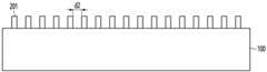
第二线圈构件1410可以定义为包括基板100、设置在基板100上的线圈电极210以及虚设电极500的线圈构件。线圈构件可以设置在上文描述的柔性印刷电路板1420上。The
参考图2和图3,线圈构件可以包括基板100以及设置在基板100的上表面和下表面上的线圈电极210、220。Referring to FIGS. 2 and 3 , the coil member may include a
基板100可以包括弯曲表面。详细地,基板100的内侧可以包括弯曲表面。The
基板100可以包括第一区域1A和第二区域2A。详细地,基板100可以包括设置有线圈电极210、220和虚设电极500的第一区域1A,以及未设置线圈电极210、220和虚设电极500的第二区域2A。The
第一区域1A可以定义为基板100的上表面和另一表面的区域。此外,第二区域2A可以定义为穿透基板100的上表面和另一表面的孔区域。The
第二区域2A的孔可以是与上文描述的通孔1421相对应的区域。也就是说,基板100的第二区域2A可以对应于透镜单元,并且可以形成为在基板的中心处穿透基板100。The holes of the
此外,第一区域1A可以形成为围绕第二区域2A。用于与设置在线圈构件下方的FPCB耦合的多个耦合孔h可以形成在第一区域1A中。详细地,将要耦合到设置在线圈构件下方的FPCB的多个耦合孔h可以形成在基板100的拐角区域中。Also, the
基板100可以是柔性基板。也就是说,基板100可以包含柔性塑料。例如,基板100可以是聚酰亚胺(PI)基板。然而,实施例不限于此,并且可以是由诸如聚对苯二甲酸乙二醇酯(PET)或聚萘二甲酸乙二醇酯(PEN)的聚合物材料制成的基板。因此,包括基板100的柔性电路板可以用于设置有弯曲显示装置的各种电子装置。The
基板100可以是绝缘基板。也就是说,基板100可以是支撑各种布线图案的绝缘基板。The
基板100可以具有20μm至100μm的厚度。例如,基板100可以具有25μm至50μm的厚度。例如,基板100可以具有30μm至40μm的厚度。当基板100的厚度超过100μm时,线圈构件的总厚度可能增大。此外,当基板100的厚度小于20μm时,在形成基板100的线圈电极的工艺中,基板100可能容易受到热/压力等的影响。The
参考图2和图3,线圈电极200可以设置在基板100上。详细地,参考图2,多个第一线圈电极210可以设置在基板100的上表面上。此外,参考图3,多个第二线圈电极220可以设置在基板100的下表面上。Referring to FIGS. 2 and 3 , the coil electrode 200 may be disposed on the
第一线圈电极210可以包括彼此间隔开的多个第一图案电极。此外,第二线圈电极220可以包括彼此间隔开的多个第二图案电极。The
参考图2,四个第一线圈电极210可以设置在基板100的上表面上。详细地,多个第一线圈电极210可以设置为在基板100的上表面上在与基板100的边缘区域相对应的区域中彼此间隔开。也就是说,第一线圈电极210中的每一个可以设置在与耦合孔h相对应的区域上。Referring to FIG. 2 , four
详细地,1-1线圈电极211、1-2线圈电极212、1-3线圈电极213和1-4线圈电极214形成在基板100的上表面上。In detail, 1-1
1-1线圈电极211、1-2线圈电极212、1-3线圈电极213和1-4线圈电极214可以设置为在基板100的上表面上彼此间隔开。The 1-1
1-1线圈电极211、1-2线圈电极212、1-3线圈电极213和1-4线圈电极214中的每一个可以以梯形形状形成在基板100的上表面上。详细地,1-1线圈电极211、1-2线圈电极212、1-3线圈电极213和1-4线圈电极214可以以梯形形状形成,其中短边在基板100的外侧,长边在基板100的内侧面对短边。也就是说,1-1线圈电极211、1-2线圈电极212、1-3线圈电极213和1-4线圈电极214的梯形形状可以形成为在从基板100的边缘向基板100的中心延伸的同时梯形形状的宽度增大。Each of the 1-1
多个第一线圈电极210可以成对地设置为彼此面对。例如,1-1线圈电极211和1-4线圈电极214被设置为在对角线方向上彼此面对,并且1-2线圈电极212和1-3线圈电极213可以设置为在对角线方向上彼此面对。The plurality of
1-1线圈电极211和1-4线圈电极214可以通过连接到1-1线圈电极211和1-4线圈电极214的连接电极300、第二线圈电极220以及多个通路孔彼此连接。The 1-1
此外,参考图3,四个第二线圈电极220可以设置在基板100的下表面上。具体地,2-1线圈电极221、2-2线圈电极222、2-3线圈电极223和2-4线圈电极224设置在基板100的下表面上。In addition, referring to FIG. 3 , four
2-1线圈电极221、2-2线圈电极222、2-3线圈电极223和2-4线圈电极224可以设置为在基板100的下表面上彼此间隔开。The 2-1
2-1线圈电极221、2-2线圈电极222、2-3线圈电极223和2-4线圈电极224中的每一个可以以梯形形状形成在基板100的下表面上。详细地,2-1线圈电极221、2-2线圈电极222、2-3线圈电极223和2-4线圈电极224可以以梯形形状形成,其中短边在基板100的外侧,长边在基板100的内侧面对短边。也就是说,2-1线圈电极221、2-2线圈电极222、2-3线圈电极223和2-4线圈电极224的梯形形状可以形成为在从基板100的边缘向基板100的中心延伸的同时梯形形状的宽度增大。Each of the 2-1
多个第二线圈电极220可以成对地设置为彼此面对。例如,2-1线圈电极221和2-4线圈电极224被设置为在对角线方向上彼此面对,并且2-2线圈电极222和2-3线圈电极223可以设置为在对角线方向上彼此面对。A plurality of
2-1线圈电极221和2-4线圈电极224可以连接到基板100的下表面上的第一布线单元410和第四布线单元440。The 2-1
2-2线圈电极222和2-3线圈电极223可以连接到基板100的下表面上的第二布线单元420和第三布线单元430。The 2-2
第一布线单元410、第二布线单元420、第三布线单元430和第四布线单元440可以仅设置在基板100的下表面上。详细地,第一布线单元410、第二布线单元420、第三布线单元430和第四布线单元440可以仅设置在基板100的面对柔性印刷电路板1420的下表面上。The
第一布线单元410、第二布线单元420、第三布线单元430和第四布线单元440可以包括与第一线圈电极、第二线圈电极和虚设电极相同或相似的材料。详细地,第一布线单元410、第二布线单元420、第三布线单元430和第四布线单元440包含铜(Cu)。然而,实施例不限于此,第一布线单元410、第二布线单元420、第三布线单元430和第四布线单元440可以包含铜(Cu)、铝(Al)、铬(Cr)、镍(Ni)、银(Ag)、钼(Mo)、金(Au)、钛(Ti)及其合金中的至少一种。The
此外,表面处理层可以进一步设置在第一布线单元410、第二布线单元420、第三布线单元430和第四布线单元440的外表面上。详细地,被设置为围绕布线单元的表面处理层可以设置在第一布线单元410、第二布线单元420、第三布线单元430和第四布线单元440的外表面上。Also, a surface treatment layer may be further provided on the outer surfaces of the
表面处理层可以包含锡(Sn)。当表面处理层形成在布线部的外表面上时,由于锡(Sn)的耐蚀性优异,所以可以防止布线部的氧化,并且可以提高线圈构件的可靠性。The surface treatment layer may contain tin (Sn). When the surface treatment layer is formed on the outer surface of the wiring portion, since tin (Sn) is excellent in corrosion resistance, oxidation of the wiring portion can be prevented, and the reliability of the coil member can be improved.
第一线圈电极210和第二线圈电极220可以在基板100的上表面和下表面上设置在彼此对应的位置处。The
也就是说,1-1线圈电极211和2-1线圈电极221可以在基板100的上表面和下表面上设置在彼此对应的位置处。此外,1-2线圈电极212和2-2线圈电极222可以在基板100的上表面和下表面上设置在彼此对应的位置处。此外,1-3线圈电极213和2-3线圈电极223可以在基板100的上表面和下表面上设置在彼此对应的位置处。此外,1-4线圈电极214和2-4线圈电极224可以在基板100的上表面和下表面上设置在彼此对应的位置处。That is, the 1-1
也就是说,设置在基板100的上表面和下表面上的线圈电极可以在基板100的上表面和下表面上设置在彼此对应的位置处,并且可以在基板的厚度方向上设置在彼此重叠的位置处。That is, the coil electrodes provided on the upper and lower surfaces of the
另一方面,第一线圈电极210和第二线圈电极220在基板100上形成由感光膜形成的感光图案,然后第一线圈电极210和第二线圈电极220可以通过电解镀工艺或无电解镀工艺形成为在感光图案之间具有预定厚度。On the other hand, the
例如,在包含绝缘材料的基板的一个表面和与该一个表面相对的另一个表面上形成感光材料后,蚀刻感光材料以形成彼此间隔开的多个感光图案。For example, after a photosensitive material is formed on one surface of a substrate including an insulating material and the other surface opposite to the one surface, the photosensitive material is etched to form a plurality of photosensitive patterns spaced apart from each other.
然后,在感光材料图案之间设置种子层之后,可以通过电解镀工艺设置形成线圈电极的镀层。也就是说,镀层可以由至少两层形成。Then, after disposing the seed layer between the photosensitive material patterns, the plating layer forming the coil electrode may be disposed through an electrolytic plating process. That is, the plating layer may be formed of at least two layers.
镀层可以包含铜(Cu)。然而,实施例不限于此,并且镀层可以包含铜(Cu)、铝(Al)、铬(Cr)、镍(Ni)、银(Ag)、钼(Mo)、金(Au)、钛(Ti)及其合金中的至少一种。The plating layer may contain copper (Cu). However, the embodiment is not limited thereto, and the plating layer may include copper (Cu), aluminum (Al), chromium (Cr), nickel (Ni), silver (Ag), molybdenum (Mo), gold (Au), titanium (Ti) ) and at least one of its alloys.
然后,通过剥离感光图案,可以在基板的两个表面上形成彼此间隔开且各自具有恒定线宽和厚度的第一线圈电极和第二线圈电极。Then, by peeling off the photosensitive pattern, first and second coil electrodes spaced apart from each other and each having a constant line width and thickness can be formed on both surfaces of the substrate.
或者,可以通过其他方法形成镀层。Alternatively, the plating layer may be formed by other methods.
详细地,在包含绝缘材料的基板的一个表面和与该一个表面相对的另一个表面上形成感光材料之后,蚀刻感光材料以形成彼此间隔开的多个感光图案。In detail, after the photosensitive material is formed on one surface of the substrate including the insulating material and the other surface opposite to the one surface, the photosensitive material is etched to form a plurality of photosensitive patterns spaced apart from each other.
然后,在感光材料图案之间设置种子层之后,可以通过电解镀工艺设置形成线圈电极的镀层。也就是说,镀层可以由至少两层形成。Then, after disposing the seed layer between the photosensitive material patterns, the plating layer forming the coil electrode may be disposed through an electrolytic plating process. That is, the plating layer may be formed of at least two layers.
镀层可以包含铜(Cu)。然而,实施例不限于此,并且镀层可以包含铜(Cu)、铝(Al)、铬(Cr)、镍(Ni)、银(Ag)、钼(Mo)、金(Au)、钛(Ti)及其合金中的至少一种。The plating layer may contain copper (Cu). However, the embodiment is not limited thereto, and the plating layer may include copper (Cu), aluminum (Al), chromium (Cr), nickel (Ni), silver (Ag), molybdenum (Mo), gold (Au), titanium (Ti) ) and at least one of its alloys.
然后,可以剥离感光图案,并且可以通过快速蚀刻去除种子层。Then, the photosensitive pattern can be stripped, and the seed layer can be removed by flash etching.
然后,可以通过电解镀工艺在镀层上形成多个镀层,以形成被形成为多层镀层的第一线圈电极和第二线圈电极。Then, a plurality of plating layers may be formed on the plating layer through an electrolytic plating process to form first and second coil electrodes formed as multi-layer plating layers.
在这种情况下,由于剥离感光图案后形成的镀层的形状不受感光图案控制,所以镀层的上表面会包括弯曲表面。In this case, since the shape of the plating layer formed after peeling the photosensitive pattern is not controlled by the photosensitive pattern, the upper surface of the plating layer may include a curved surface.
同时,第一线圈电极210和第二线圈电极220可以通过连接电极300和多个通路孔电连接。Meanwhile, the
详细地,多个通路孔可以形成在基板100上。例如,形成在第一线圈电极210和第二线圈电极220的内侧区域中的至少一个通路孔可以设置在基板100上。并且,形成在第一线圈电极210和第二线圈电极220的外侧区域中的至少一个通路孔可以设置在基板100上。In detail, a plurality of via holes may be formed on the
图4和图5是用于说明第一线圈电极210和第二线圈电极220之间的连接关系的视图,其中省略了设置在基板上的虚设电极500。4 and 5 are views for explaining the connection relationship between the
参考图4和图5,X通道的1-1线圈电极211、1-4线圈电极214、2-1线圈电极221和2-4线圈电极224可以通过多个连接电极和通路孔在从第一布线单元410到第四布线单元440的方向上连接。4 and 5, the 1-1
此外,Y通道的1-2线圈电极212、1-3线圈电极213、2-2线圈电极222和2-3线圈电极223可以通过多个连接电极和通路孔在从第二布线单元420到第三布线单元430的方向上连接。In addition, the 1-2
详细地,在第一布线单元410的方向上施加的电流通过连接电极300移动到第2-1线圈电极221。然后,其移动到2-1线圈电极221的内侧,并通过第一通路孔V1移动到1-1线圈电极211。然后,其移动到1-1线圈电极211的外侧,并通过连接电极300移动到1-4线圈电极214。然后,其移动到1-4线圈电极214的内侧,并通过第二通路孔V2移动到2-4线圈电极224。然后,其可以移动到2-4线圈电极224的外侧,以通过连接电极连接到第四布线单元440。In detail, the current applied in the direction of the
在这种情况下,第一通路孔V1和第二通路孔V2可以形成在线圈电极的内侧区域中。In this case, the first via hole V1 and the second via hole V2 may be formed in the inner region of the coil electrode.
此外,在第二布线单元420的方向上施加的电流通过连接电极300移动到2-2线圈电极222。然后,其移动到2-2线圈电极222的内侧,并通过第三通路孔V3移动到1-2线圈电极212。然后,其移动到1-2线圈电极212的外侧,并通过第四通路孔V4、第五通路孔V5和连接电极300到达1-3线圈电极213。然后,其移动到1-3线圈电极213的内侧,并通过第六通路孔V6移动到2-3线圈电极223。然后,其可以移动到第2-3线圈电极223的外侧,以通过连接电极连接到第三布线单元430。Further, the current applied in the direction of the
在这种情况下,第三通路孔V3和第六通路孔V6可以形成在线圈电极的内侧区域中,第四通路孔V4和第五通路孔V5可以形成在线圈电极的外侧区域中。In this case, the third via hole V3 and the sixth via hole V6 may be formed in the inner region of the coil electrode, and the fourth via hole V4 and the fifth via hole V5 may be formed in the outer region of the coil electrode.
也就是说,X通道和Y通道可以通过连接电极和多个通路孔分别连接到第一线圈电极210和第二线圈电极220。具体地,可以通过多个通路孔减小连接电极的长度。因此,通过最小化连接电极的长度,可以减小线圈构件的尺寸。此外,通过减小连接电极的长度,可以防止电阻随着连接电极长度的增大而增大,从而提高线圈构件的特性。That is, the X channel and the Y channel may be connected to the
同时,在根据本实施例的线圈构件中,可以通过不同地控制每个区域的第一线圈电极和第二线圈电极的图案电极的线宽来减小线圈构件的电阻。Meanwhile, in the coil member according to the present embodiment, the resistance of the coil member can be reduced by differently controlling the line widths of the pattern electrodes of the first coil electrode and the second coil electrode of each region.
参考图6,第一线圈电极210可以在一个方向上延伸,同时具有多个弯曲区域。因此,第一线圈电极210可以整体以线圈图案形状形成。例如,第一线圈电极210的图案电极可以形成为线圈状电极,同时在从外到内或从内到外的一个方向上延伸。Referring to FIG. 6 , the
第一线圈电极210通过由于电流的变化而改变磁通量来产生电动势。由第一线圈电极210产生的磁通量可以与电感和流动电流成比例,如以下等式所示。此外,电动势会受电路的电阻影响,并且随着第一线圈电极210的横截面积增大,电阻可以减小。The
[等式1][Equation 1]
Φ=LlΦ=Ll
[等式2][Equation 2]
L=μN2A/lL=μN2A/l
[等式3][Equation 3]
电阻=l/导电率*AResistance=l/Conductivity*A
(在等式1至等式3中,Φ是磁通量,L是电感,N是线圈电极的匝数,l是线圈的长度,A是面积(线圈电极的线宽*厚度)。(In
也就是说,为了减小电路的电阻,需要增大第一线圈电极210的横截面积或者减小第一线圈电极210的长度。然而,当第一线圈电极210的长度减小时,第一线圈电极的磁通量减小,从而电动势减小,因此特性可能变差。That is, in order to reduce the resistance of the circuit, it is necessary to increase the cross-sectional area of the
因此,根据本实施例的线圈构件可以在保持第一线圈电极210的长度的同时,通过增大第一线圈电极210的线宽来增大第一线圈电极210的横截面积。因此,可以减小线圈构件的电阻。Therefore, the coil member according to the present embodiment can increase the cross-sectional area of the
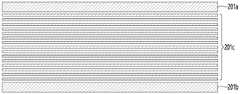
参考图6至图8,第一线圈电极210可以包括彼此间隔开的多个第一图案电极。可以根据图案电极的各个位置来划分第一线圈电极210的图案电极。例如,当靠近第二区域2A的区域被定义为内侧并且靠近耦合孔h的区域被定义为外侧时,第一线圈电极210可以包括第一最外侧图案电极201a、第一最内侧图案电极201b和第一中心图案电极201c。Referring to FIGS. 6 to 8 , the
详细地,第一最外侧图案电极201a可以定义为图案电极中的最外侧图案电极,第一最内侧图案电极201b可以定义为图案电极中的最内侧图案电极。In detail, the first
虚设电极500可以设置在彼此面对的第一最内侧图案电极201b之间。此外,虚设电极500可以设置在第一最外侧图案电极201a的外侧。The
虚设电极500可以使第一线圈电极210和第二线圈电极220的每个图案电极的镀层厚度均匀。The
详细地,当只有用于形成第一线圈电极210和第二线圈电极220的感光图案形成在基板100上时,可能难以均匀地控制第一线圈电极210和第二线圈电极220的图案电极的整体镀层厚度。因此,除第一线圈电极210和第二线圈电极220的图案电极之外,还可以另外形成作为虚设电极的图案电极的感光图案。因此,可以使基板的每个区域中的镀层区域均匀。因此,第一线圈电极210和第二线圈电极220的图案电极的镀层厚度可以是均匀的。In detail, when only the photosensitive pattern for forming the
也就是说,虚设电极500可以部分地或全部地形成在除形成有第一线圈电极210和第二线圈电极220的区域之外的区域中。That is, the
第一最外侧图案电极201a、第一最内侧图案电极201b和第一中心图案电极201c可以定义为与磁体部1310重叠的区域。详细地,第一线圈电极210的第一最外侧图案电极201a、第一最内侧图案电极201b和第一中心图案电极201c可以与设置在线圈构件上的磁体部1310垂直地重叠。The first
详细地,第一最外侧图案电极201a的整个区域可以设置为与磁体部1310重叠。或者,第一最外侧图案电极201a的一个区域可以与磁体部1310重叠,而第一最外侧图案电极201a的其他区域可以不与磁体部1310重叠。In detail, the entire area of the first
此外,第一最内侧图案电极201b的整个区域可以设置为与磁体部1310重叠。或者,第一最内侧图案电极201b的一个区域可以与磁体部1310重叠,而第一最内侧图案电极201b的其他区域可以不与磁体部1310重叠。Also, the entire area of the first
也就是说,设置有第一最外侧图案电极201a和第一最内侧图案电极201b的基板区域可以定义为图案电极和磁体部1310可以重叠的临界区域。That is, the substrate area where the first
也就是说,即使图案电极进一步设置在第一最外侧图案电极201a的外侧和第一最内侧图案电极201b的内侧,进一步设置的图案电极也不会与磁体部1310重叠。因此,线圈的长度增大,但可能没有电动势效应。That is, even if the pattern electrode is further provided outside the first
第一最外侧图案电极201a、第一最内侧图案电极201b和第一中心图案电极201c可以设置为彼此间隔开。The first
详细地,第一最外侧图案电极201a和第一中心图案电极201c可以设置为以第一间距d1间隔开,第一最内侧图案电极201b和第一中心图案电极201c可以设置为以第二间距d2彼此间隔开,并且多个第一中心图案电极201c可以设置为以第三间距d3彼此间隔开。In detail, the first
第一间距d1、第二间距d2和第三间距d3可以具有相同或相似的大小。The first distance d1, the second distance d2 and the third distance d3 may have the same or similar size.
例如,第一间距d1、第二间距d2和第三间距d3可以是5μm至15μm的间距S1、S2。详细地,第一间距d1、第二间距d2和第三间距d3可以是7μm至13μm的间距。更详细地,第一间距d1、第二间距d2和第三间距d3可以是9μm至11μm的间距。For example, the first pitch d1 , the second pitch d2 and the third pitch d3 may be pitches S1 , S2 of 5 μm to 15 μm. In detail, the first pitch d1 , the second pitch d2 and the third pitch d3 may be pitches of 7 μm to 13 μm. In more detail, the first pitch d1 , the second pitch d2 and the third pitch d3 may be pitches of 9 μm to 11 μm.
当第一间距d1、第二间距d2和第三间距d3形成为小于5μm时,在形成第一线圈电极210时,感光图案可能由于感光图案的线宽减小而塌陷。因此,由于线圈电极的图案电极彼此短路,从而每个线圈电极的各个图案电极的线宽可能变得不均匀。此外,当第一间距d1、第二间距d2和第三间距d3形成为超过15μm时,第一线圈电极210的长度可能整体增大。When the first pitch d1 , the second pitch d2 and the third pitch d3 are formed to be less than 5 μm, the photosensitive pattern may collapse due to a reduction in the line width of the photosensitive pattern when the
第一最外侧图案电极201a、第一最内侧图案电极201b和第一中心图案电极201c可以具有不同的线宽。详细地,第一最外侧图案电极201a的线宽w1和第一最内侧图案电极201b的线宽w2可以大于第一中心图案电极201c的线宽w3。也就是说,第一线圈电极210的图案电极中的最外侧图案电极和最内侧图案电极的线宽可以大于最外侧图案电极和最内侧图案电极之间的中心图案电极的线宽。The first
也就是说,与磁体部重叠的设置在临界区域中的最外侧图案电极和最内侧图案电极的线宽可以形成为大于中心图案电极的线宽。That is, the line widths of the outermost pattern electrodes and the innermost pattern electrodes provided in the critical region overlapping the magnet portions may be formed to be larger than the line widths of the center pattern electrodes.
因此,可以增大第一线圈电极的图案电极的线宽,并且可以通过增大图案电极的线宽来减小第一线圈电极的电阻。Therefore, the line width of the pattern electrode of the first coil electrode can be increased, and the resistance of the first coil electrode can be reduced by increasing the line width of the pattern electrode.
例如,第一最外侧图案电极201a的线宽w1和第一最内侧图案电极201b的线宽w2可以比第一中心图案电极201c的线宽w3大1倍且小于或等于线宽w3的10倍。For example, the line width w1 of the first
第一最外侧图案电极201a的线宽w1和第一最内侧图案电极201b的线宽w2等于或小于第一中心图案电极201c的线宽w3大小的1倍,可能无法实现由于第一最外侧图案电极201a的线宽w1和第一最内侧图案电极201b的线宽w2而减小电阻的效果。The line width w1 of the first
第一最外侧图案电极201a的线宽w1和第一最内侧图案电极201b的线宽w2超过第一中心图案电极201c的线宽w3大小的10倍,由于第一最外侧图案电极201a的线宽w1和第一最内侧图案电极201b的线宽w2而减小电阻的效果较小,并且可能会增大线圈构件的尺寸。The line width w1 of the first
例如,第一中心图案电极201c的线宽w3可以是约22μm至约32μm。此外,第一最外侧图案电极201a的线宽w1和第一最内侧图案电极201b的线宽w2可以是约30μm至330μm。For example, the line width w3 of the first
在线宽范围内,第一最外侧图案电极201a的线宽w1和第一最内侧图案电极201b的线宽w2可以大于第一中心图案电极201c的线宽w3。此外,在线宽范围内,第一最外侧图案电极201a的线宽w1和第一最内侧图案电极201b的线宽w2可以形成为具有相同或不同的线宽。Within the line width range, the line width w1 of the first
同时,参考图9至图11,第二线圈电极220的图案电极可以类似于第一线圈电极210的图案电极形成。Meanwhile, referring to FIGS. 9 to 11 , the pattern electrodes of the
详细地,参考图9至图11,第二线圈电极220可以包括彼此间隔开的多个第二图案电极。可以根据图案电极的各个位置来划分第二线圈电极220的图案电极。例如,当靠近第二区域2A的区域被定义为内侧并且靠近耦合孔h的区域被定义为外侧时,第二线圈电极210可以包括第二最外侧图案电极202a、第二最内侧图案电极202b和第二中心图案电极202c。虚设电极500可以设置在彼此面对的第二最内侧图案电极202b之间。此外,虚设电极500可以设置在第二最外侧图案电极202a的外侧。In detail, referring to FIGS. 9 to 11 , the
详细地,第二最外侧图案电极202a可以定义为图案电极中的最外侧图案电极,第二最内侧图案电极202b可以定义为图案电极中的最内侧图案电极。In detail, the second
第二最外侧图案电极202a、第二最内侧图案电极202b和第二中心图案电极202c可以定义为与磁体部1310重叠的区域。详细地,第二线圈电极220的第二最外侧图案电极202a、第二最内侧图案电极202b和第二中心图案电极202c可以与设置在线圈构件上的磁体部1310垂直地重叠。The second
详细地,第二最外侧图案电极202a的整个区域可以设置为与磁体部1310重叠。或者,第二最外侧图案电极202a的一个区域可以与磁体部1310重叠,而第二最外侧图案电极202a的其他区域可以不与磁体部1310重叠。In detail, the entire area of the second
此外,第二最内侧图案电极202b的整个区域可以设置为与磁体部1310重叠。或者,第二最内侧图案电极202b的一个区域可以与磁体部1310重叠,而第二最内侧图案电极202b的其他区域可以不与磁体部1310重叠。Also, the entire area of the second
也就是说,设置有第二最外侧图案电极202a和第二最内侧图案电极202b的基板区域可以定义为图案电极和磁体部1310可以重叠的临界区域。That is, the substrate area where the second
也就是说,即使图案电极进一步设置在第二最外侧图案电极202a的外侧和第二最内侧图案电极202b的内侧,进一步设置的图案电极也不会与磁体部1310重叠。因此,线圈的长度增大,但可能没有电动势效应。That is, even if the pattern electrode is further provided outside the second
第二最外侧图案电极202a、第二最内侧图案电极202b和第二中心图案电极202c可以设置为彼此间隔开。The second
详细地,第二最外侧图案电极202a和第二中心图案电极202c可以设置为以第一’间距d1’间隔开,第二最内侧图案电极202b和第二中心图案电极202c可以设置为以第二’间距d2’彼此间隔开,并且多个第二中心图案电极202c可以设置为以第三’间距d3’彼此间隔开。In detail, the second
第一’间距d1’、第二’间距d2’和第三’间距d3’可以具有相同或相似的大小。The first 'spacing d1', the second 'spacing d2' and the third 'spacing d3' may have the same or similar size.
例如,第一’间距d1’、第二’间距d2’和第三’间距d3’可以是5μm至15μm的间距S1、S2。详细地,第一’间距d1’、第二’间距d2’和第三’间距d3’可以是7μm至13μm的间距。更详细地,第一’间距d1’、第二’间距d2’,第三’间距d3’可以是9μm至11μm的间距。For example, the first 'spacing d1', the second 'spacing d2' and the third 'spacing d3' may be the spacings S1, S2 of 5 μm to 15 μm. In detail, the first 'pitch d1', the second 'pitch d2' and the third 'pitch d3' may be pitches of 7µm to 13µm. In more detail, the first 'pitch d1', the second 'pitch d2', and the third 'pitch d3' may be pitches of 9 μm to 11 μm.
当第一’间距d1’、第二’间距d2’和第三’间距d3’形成为小于5μm时,在形成第二线圈电极220时,感光图案可能由于感光图案的线宽减小而塌陷。因此,由于线圈电极的图案电极彼此短路,从而每个线圈电极的各个图案电极的线宽可能变得不均匀。此外,当第一’间距d1’、第二’间距d2’和第三’间距d3’形成为超过15μm时,第二线圈电极220的长度可能整体增大。When the first 'pitch d1', the second 'pitch d2', and the third 'pitch d3' are formed to be less than 5 μm, when the
同时,上文描述的第一间距d1、第二间距d2和第三间距d3是第一’间距d1’、第二’间距d2’和第三’间距d3’,并且在上述范围内可以彼此相同或不同。Meanwhile, the first pitch d1 , the second pitch d2 and the third pitch d3 described above are the first ' pitch d1 ', the second ' pitch d2 ' and the third ' pitch d3 ', and may be the same as each other within the above range or different.
第二最外侧图案电极202a、第二最内侧图案电极202b和第二中心图案电极202c可以具有不同的线宽。详细地,第二最外侧图案电极202a的线宽w1’和第二最内侧图案电极202b的线宽w2’可以大于第二中心图案电极202c的线宽w3’。也就是说,第二线圈电极220的图案电极中的最外侧图案电极和最内侧图案电极的线宽可以大于最外侧图案电极和最内侧图案电极之间的中心图案电极的线宽。The second
也就是说,与磁体部重叠的设置在临界区域中的最外侧图案电极和最内侧图案电极的线宽可以形成为大于中心图案电极的线宽。That is, the line widths of the outermost pattern electrodes and the innermost pattern electrodes provided in the critical region overlapping the magnet portions may be formed to be larger than the line widths of the center pattern electrodes.
因此,可以增大第二线圈电极的图案电极的线宽,并且可以通过增大图案电极的线宽来减小第二线圈电极的电阻。Therefore, the line width of the pattern electrode of the second coil electrode can be increased, and the resistance of the second coil electrode can be reduced by increasing the line width of the pattern electrode.
例如,第二最外侧图案电极202a的线宽w1’和第二最内侧图案电极202b的线宽w2’可以比第二中心图案电极202c的线宽w3’大1倍且小于或等于线宽w3’的10倍。For example, the line width w1' of the second
第二最外侧图案电极202a的线宽w1’和第二最内侧图案电极202b的线宽w2’等于或小于第二中心图案电极202c的线宽w3’大小的1倍,可能无法实现由于第二最外侧图案电极202a的线宽w1’和第二最内侧图案电极202b的线宽w2’而减小电阻的效果。The line width w1' of the second
第二最外侧图案电极202a的线宽w1’和第二最内侧图案电极202b的线宽w2’超过第二中心图案电极202c的线宽w3’大小的10倍,由于第二最外侧图案电极202a的线宽w1’和第二最内侧图案电极202b的线宽w2’而减小电阻的效果较小,并且可能会增大线圈构件的尺寸。The line width w1' of the second
例如,第二中心图案电极202c的线宽w3’可以是约22μm至约32μm。此外,第二最外侧图案电极202a的线宽w1’和第二最内侧图案电极202b的线宽w2’可以是约30μm至330μm。For example, the line width w3' of the second
在线宽范围内,第二最外侧图案电极202a的线宽w1’和第二最内侧图案电极202b的线宽w2’可以大于第二中心图案电极202c的线宽w3’。此外,在线宽范围内,第二最外侧图案电极202a的线宽w1’和第二最内侧图案电极202b的线宽w2’可以形成为具有相同或不同的线宽。Within the line width range, the line width w1' of the second
此外,在上述范围内,第一最外侧图案电极201a的线宽w1和第二最外侧图案电极202a的线宽w1’可以彼此相同或不同。此外,在上述范围内,第一最内侧图案电极201b的线宽w2和第二最内侧图案电极202b的线宽w2’可以彼此相同或不同。Further, within the above range, the line width w1 of the first
参考图12,在基板100的两个表面上,第一最外侧图案电极201a和第二最外侧图案电极202a设置在相应位置处,第一最内侧图案电极201b和第二最内侧图案电极202b设置在相应位置处,第一中心图案电极201c和第二中心图案电极202c设置在相应位置处。此外,第一最外侧图案电极201a的线宽和第一最内侧图案电极201b的线宽大于第一中心图案电极201c的线宽,第二最外侧图案电极202a的线宽和第二最内侧图案电极202b的线宽大于第二中心图案电极202c的线宽。Referring to FIG. 12 , on both surfaces of the
在根据本实施例的线圈构件中,线圈电极的图案电极中的设置在最外侧和/或最内侧的图案电极的线宽可以与中心图案电极的线宽不同。In the coil member according to the present embodiment, the line width of the pattern electrodes disposed at the outermost and/or innermost among the pattern electrodes of the coil electrodes may be different from the line width of the center pattern electrode.
详细地,线圈电极的图案电极中的最外侧图案电极和/或最内侧图案电极的线宽可以形成为大于中心图案电极的线宽。In detail, the line width of the outermost pattern electrode and/or the innermost pattern electrode among the pattern electrodes of the coil electrode may be formed to be larger than that of the center pattern electrode.
因此,通过增大线圈电极的线宽(其为线圈电极的电阻的一个变量),可以减小线圈电极的电阻。Therefore, by increasing the line width of the coil electrodes, which is a variable of the resistance of the coil electrodes, the resistance of the coil electrodes can be reduced.
因此,通过减小线圈电极的电阻,可以提高线圈构件和包括该线圈构件的摄像头模块的特性。Therefore, by reducing the resistance of the coil electrode, the characteristics of the coil member and the camera module including the coil member can be improved.
此外,在根据本实施例的线圈构件中,可以通过多个通路孔连接多个单元线圈电极。Furthermore, in the coil member according to the present embodiment, a plurality of unit coil electrodes can be connected through a plurality of via holes.
因此,可以减小连接单元线圈电极的连接电极的长度和布置面积。因此,可以防止由于连接电极的长度增大而导致电阻增大,并且可以通过最小化布置面积来减小线圈构件的尺寸Therefore, the length and arrangement area of the connection electrodes of the connection unit coil electrodes can be reduced. Therefore, an increase in resistance due to an increase in the length of the connection electrodes can be prevented, and the size of the coil member can be reduced by minimizing the arrangement area
在下文中,将参考图13至图20描述根据另一个实施例的线圈构件。Hereinafter, a coil member according to another embodiment will be described with reference to FIGS. 13 to 20 .
在根据另一个实施例的线圈构件中,可以通过不同地控制每个区域的第一线圈电极和第二线圈电极的图案电极之间的间距来提高线圈构件的可靠性。In the coil member according to another embodiment, the reliability of the coil member can be improved by differently controlling the spacing between the pattern electrodes of the first coil electrode and the second coil electrode of each region.
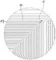
参考图13,第一线圈电极210可以在一个方向上延伸,同时具有多个弯曲区域。Referring to FIG. 13 , the
因此,第一线圈电极210可以整体以线圈图案形状形成。例如,第一线圈电极210的第一图案电极201可以形成为线圈状电极,同时在从外到内或从内到外的一个方向上延伸。Therefore, the
第一线圈电极210可以包括根据第一图案电极的方向定义的第一区域1A、第二区域2A和第三区域3A。详细地,第一线圈电极可以包括第一图案电极201在第一方向上延伸的第一区域1A,第一图案电极201在与第一方向不同的方向上延伸的第二区域2A,以及在第一图案电极201中的第一区域1A和第二区域2A之间第一图案电极201的方向改变的第三区域3A。The
详细地,第一区域1A和第二区域2A可以是第一图案电极201沿直线(即,一个方向)延伸的区域,第三区域3A可以是图案电极的方向从一个方向改变为另一个方向的区域。In detail, the
也就是说,第三区域3A可以是第一线圈电极210弯曲的区域。That is, the
第三区域3A的数量可以根据第一区域1A和第二区域2A的方向而改变。例如,参考图6,第一线圈电极210可以在一个方向上延伸,同时具有四个第三区域3A。The number of the
参考图14至图16,每个区域的第一线圈电极210的第一图案电极之间的间距可以不同。详细地,第一线圈电极210的第一图案电极之间的间距可以在第一区域1A、第二区域2A和第三区域3A中彼此不同。Referring to FIGS. 14 to 16 , the spacing between the first pattern electrodes of the
例如,在第一线圈电极210中,第一图案电极201在第一区域1A和第二区域2A中以第一间距d1间隔开,第一图案电极201在第三区域3A中以第二间距d2间隔开。For example, in the
在这种情况下,第一间距d1和第二间距d2可以定义为相邻的第一图案电极之间的距离。In this case, the first pitch d1 and the second pitch d2 may be defined as distances between adjacent first pattern electrodes.
在这种情况下,第一间距d1和第二间距d2的大小可以彼此不同。详细地,第二间距d2的大小可以大于第一间距d1的大小。也就是说,在第一线圈电极的图案电极201的方向改变的弯曲区域中,第一图案电极201之间的间距可以大于其他区域中的第一图案电极201之间的间距。In this case, the sizes of the first distance d1 and the second distance d2 may be different from each other. In detail, the size of the second distance d2 may be greater than that of the first distance d1. That is, in the curved region where the direction of the
同时,在第一线圈电极210中,在全部的多个第三区域中,第一图案电极201之间的间距可以大于其他区域中的第一图案电极201之间的间距。或者,仅在多个第三区域中的一部分中,第一图案电极201之间的间距可以大于其他区域中的第一图案电极201之间的间距。Meanwhile, in the
例如,当第一线圈电极210包括两对彼此面对的第三区域时,任意一对彼此面对的第三区域中的第一图案电极201之间的间距可以大于其他区域中的第一图案电极201之间的间距。或者,两对彼此面对的第三区域中的第一图案电极201之间的间距可以大于其他区域中的第一图案电极201之间的间距。For example, when the
第一间距d1和第二间距d2可以与设置在第一图案电极201之间以形成第一线圈电极210的感光图案的宽度相同。在这种情况下,在图案电极201弯曲的区域中,感光图案的宽度形成为大于其他区域中的感光图案的宽度,从而可以最小化弯曲区域中的感光图案的塌陷。The first pitch d1 and the second pitch d2 may be the same as the widths of the photosensitive patterns disposed between the
因此,可以防止感光图案在弯曲区域中塌陷、图案电极彼此短路或图案电极的形状变得不均匀。Therefore, it is possible to prevent the photosensitive pattern from collapsing in the curved region, the pattern electrodes being short-circuited to each other, or the shape of the pattern electrodes becoming uneven.
例如,第一间距d1的大小可以是5μm至15μm。当第一间距d1形成为小于5μm时,在形成第一线圈电极210时,感光图案可能由于感光图案的线宽减小而塌陷。因此,由于线圈电极的图案电极彼此短路,每个线圈电极的各个图案电极的线宽可能变得不均匀。此外,当第一间距d1形成为超过15μm时,第一线圈电极210的长度可能会整体增大。For example, the size of the first pitch d1 may be 5 μm to 15 μm. When the first pitch d1 is formed to be less than 5 μm, when the
此外,第二间距d2的大小可以是30μm至70μm。当第二间距d2形成为小于30μm时,感光图案可能在第一线圈电极的弯曲区域处塌陷。因此,由于线圈电极的图案电极彼此短路,每个线圈电极的各个图案电极的线宽可能会变得不均匀。此外,当第二间距d2形成为超过70μm时,第一线圈电极的弯曲区域中的曲率变得过大,使得第一线圈电极210的总面积可能会增大。Also, the size of the second pitch d2 may be 30 μm to 70 μm. When the second pitch d2 is formed to be less than 30 μm, the photosensitive pattern may collapse at the bent region of the first coil electrode. Therefore, since the pattern electrodes of the coil electrodes are short-circuited to each other, the line width of the respective pattern electrodes of each coil electrode may become uneven. Furthermore, when the second pitch d2 is formed to exceed 70 μm, the curvature in the curved region of the first coil electrode becomes too large, so that the total area of the
此外,第一区域1A、第二区域2A和第三区域3A中的第一图案电极201的线宽可以不同。In addition, the line widths of the
例如,第三区域3A中的第一图案电极201的线宽可以小于第一区域1A和第二区域2A中的至少一个中的第一图案电极201的线宽。For example, the line width of the
同时,参考图17至图20,第二线圈电极220的图案电极可以类似于第一线圈电极210的图案电极形成。Meanwhile, referring to FIGS. 17 to 20 , the pattern electrodes of the
参考图17,第二线圈电极220可以在一个方向上延伸,同时具有多个弯曲区域。Referring to FIG. 17 , the
因此,第二线圈电极220可以整体以线圈图案形状形成。例如,第二线圈电极220的第二图案电极202可以形成为线圈状电极,同时在从外到内或从内到外的一个方向上延伸。Therefore, the
第二线圈电极220可以包括根据第二图案电极的方向定义的第一’区域1’A、第二’区域2’A和第三’区域3’A。详细地,第二线圈电极可以包括第二图案电极202在第一方向上延伸的第一’区域1’A,第二图案电极202在与第一方向不同的方向上延伸的第二’区域2’A,以及在第二图案电极202中的第一’区域1’A和第二’区域2’A之间第二图案电极202的方向改变的第三’区域3’A。The
详细地,第一’区域1’A和第二’区域2’A可以是第二图案电极202沿直线(即,一个方向)延伸的区域,第三’区域3’A可以是图案电极的方向从一个方向改变为另一个方向的区域。In detail, the first' area 1'A and the second' area 2'A may be areas where the
也就是说,第三’区域3’A可以是第二线圈电极220弯曲的区域。That is, the third' region 3'A may be a region where the
第一区域1A和第一’区域1’A的位置可以彼此对应。并且,第二区域2A和第二’区域2’A的位置可以彼此对应。也就是说,第一区域1A和第一’区域1’A的位置可以在基板的厚度方向上彼此重叠。并且,第二区域2A和第二’区域2’A的位置可以在基板的厚度方向上彼此重叠。The positions of the
此外,第三区域3A和第三’区域3’A的位置可以彼此对应。也就是说,第三区域3A和第三’区域3’A的位置可以在基板的厚度方向上彼此重叠。Also, the positions of the
第三’区域3’A的数量可以根据第一’区域1’A和第二’区域2’A的方向而改变。例如,参考图17,第二线圈电极220可以在一个方向上延伸,同时具有四个第三’区域3’A。The number of the third' area 3'A may vary according to the orientation of the first' area 1'A and the second' area 2'A. For example, referring to Fig. 17, the
参考图18至图20,每个区域的第二线圈电极210的第二图案电极之间的间距可以不同。详细地,第二线圈电极220的第二图案电极之间的间距可以在第一’区域1’A、第二’区域2’A和第三’区域3’A中彼此不同。Referring to FIGS. 18 to 20 , the spacing between the second pattern electrodes of the
例如,在第二线圈电极220中,第二图案电极202在第一’区域1’A和第二’区域2’A中以第一’间距d1’间隔开,第二图案电极202在第三’区域3’A中以第二’间距d2’间隔开。For example, in the
在这种情况下,第一’间距d1’和第二’间距d2’可以定义为相邻的第二图案电极之间的距离。In this case, the first 'interval d1' and the second 'interval d2' may be defined as the distance between adjacent second pattern electrodes.
在这种情况下,第一’间距d1’和第二’间距d2’的大小可以彼此不同。详细地,第二’间距d2’的大小可以大于第一’间距d1’的大小。也就是说,在第二线圈电极的第二图案电极202的方向改变的弯曲区域中,第二图案电极202之间的间距可以大于其他区域中的第二图案电极202之间的间距。In this case, the sizes of the first 'interval d1' and the second 'interval d2' may be different from each other. In detail, the size of the second 'interval d2' may be greater than that of the first 'interval d1'. That is, in the curved region where the direction of the
例如,当第二线圈电极220包括两对彼此面对的第三’区域时,任意一对彼此面对的第三’区域中的第二图案电极202之间的间距可以大于其他区域中的第二图案电极202之间的间距。或者,两对彼此面对的第三’区域中的第二图案电极202之间的间距可以大于其他区域中的第二图案电极202之间的间距。For example, when the
第一’间距d1’和第二’间距d2’可以与设置在第二图案电极202之间以形成第二线圈电极220的感光图案的宽度相同。在这种情况下,在第二图案电极202弯曲的区域中,感光图案的宽度形成为大于其他区域中的感光图案的宽度,从而可以最小化弯曲区域中的感光图案的塌陷。The first 'spacing d1' and the second 'spacing d2' may be the same as the widths of the photosensitive patterns disposed between the
因此,可以防止感光图案在弯曲区域中塌陷、图案电极彼此短路或图案电极的形状变得不均匀。Therefore, it is possible to prevent the photosensitive pattern from collapsing in the curved region, the pattern electrodes being short-circuited to each other, or the shape of the pattern electrodes becoming uneven.
例如,第一’间距d1’的大小可以是5μm至15μm。当第一’间距d1’形成为小于5μm时,在形成第二线圈电极220时,感光图案可能由于感光图案的线宽减小而塌陷。因此,由于线圈电极的图案电极彼此短路,每个线圈电极的各个图案电极的线宽可能变得不均匀。此外,当第一’间距d1’形成为超过15μm时,第二线圈电极220的长度可能会整体增大。For example, the size of the first 'spacing d1' may be 5 μm to 15 μm. When the first 'pitch d1' is formed to be less than 5 μm, when the
此外,第二’间距d2’的大小可以是30μm至70μm。当第二’间距d2’形成为小于30μm时,感光图案可能在第一线圈电极的弯曲区域处塌陷。因此,由于线圈电极的图案电极彼此短路,每个线圈电极的各个图案电极的线宽可能变得不均匀。此外,当第二’间距d2’形成为超过70μm时,第二线圈电极的弯曲区域中的曲率变得过大,使得第二线圈电极220的总面积可能会增大。Also, the size of the second 'spacing d2' may be 30µm to 70µm. When the second 'pitch d2' is formed to be less than 30 μm, the photosensitive pattern may collapse at the bent region of the first coil electrode. Therefore, since the pattern electrodes of the coil electrodes are short-circuited to each other, the line width of the respective pattern electrodes of each coil electrode may become uneven. Also, when the second ' pitch d2' is formed to exceed 70 μm, the curvature in the curved region of the second coil electrode becomes too large, so that the total area of the
此外,第一’区域1’A、第二’区域2’A和第三’区域3’A中的第二图案电极202的线宽可以不同。In addition, the line widths of the
例如,第三’区域3’A中的第二图案电极202的线宽可以小于第一’区域1’A和第二’区域2’A中的至少一个中的第二图案电极202的线宽。For example, the line width of the
在根据另一个实施例的线圈构件中,每个区域的线圈电极的图案电极之间的间距可以不同。In the coil member according to another embodiment, the spacing between the pattern electrodes of the coil electrodes of each region may be different.
详细地,在线圈构件中,线圈电极的弯曲区域中的图案电极之间的间距可以大于其他区域中的图案电极之间的间距。In detail, in the coil member, the spacing between the pattern electrodes in the curved region of the coil electrode may be larger than the spacing between the pattern electrodes in other regions.
因此,在形成线圈电极时,可以增大感光图案的线宽,从而防止感光图案在弯曲区域中支撑较弱而塌陷。Therefore, when the coil electrodes are formed, the line width of the photosensitive pattern can be increased, thereby preventing the photosensitive pattern from being weakly supported and collapsing in the curved region.
也就是说,通过使以精细线宽设置的感光图案形成为在弯曲区域中比在其他区域中大,也可以在弯曲区域中稳定地形成感光图案。That is, by forming the photosensitive pattern set with the fine line width to be larger in the curved region than in other regions, the photosensitive pattern can also be stably formed in the curved region.
因此,根据另一个实施例的线圈构件可以防止弯曲区域中的线圈电极的短路和图案形状不均匀,因此,根据另一个实施例的线圈构件可以具有提高的可靠性。Therefore, the coil member according to another embodiment can prevent the short circuit of the coil electrodes in the bending region and the unevenness of the pattern shape, and thus, the coil member according to another embodiment can have improved reliability.
上文描述的实施例中描述的特征、结构、效果等包含在本发明的至少一个实施例中,但不限于仅一个实施例。此外,本领域技术人员可以针对其他实施例组合或修改每个实施例中所示的特征、结构和效果。因此,应当理解,这种组合和修改包含在本发明的范围内。The features, structures, effects, etc. described in the above-described embodiments are included in at least one embodiment of the present invention, but are not limited to only one embodiment. Furthermore, the features, structures and effects shown in each embodiment may be combined or modified for other embodiments by those skilled in the art. Therefore, it should be understood that such combinations and modifications are included within the scope of the present invention.
此外,上文主要描述了实施例,但是实施例仅仅是示例,并且不限制本发明,本领域技术人员可以理解,在不脱离实施例的基本特征的情况下,可以进行上文未呈现的各种变化和应用。例如,在实施例中具体描述的每个组件可以有所不同。此外,应当解释为,与这种变化和这种应用相关的差异包含在以下权利要求中定义的本发明的范围内。In addition, the embodiments are mainly described above, but the embodiments are only examples and do not limit the present invention, and those skilled in the art can understand that various aspects not presented above can be performed without departing from the essential characteristics of the embodiments. variations and applications. For example, each component specifically described in an embodiment may vary. Furthermore, it should be construed that differences related to such variations and such applications are included within the scope of the present invention as defined in the following claims.
Claims (10)
Translated fromChineseApplications Claiming Priority (5)
| Application Number | Priority Date | Filing Date | Title |
|---|---|---|---|
| KR1020190128657AKR102669307B1 (en) | 2019-10-16 | 2019-10-16 | Coil member for correcting hand-shake and camera module having the same |
| KR10-2019-0128657 | 2019-10-16 | ||
| KR10-2019-0128666 | 2019-10-16 | ||
| KR1020190128666AKR102770253B1 (en) | 2019-10-16 | 2019-10-16 | Coil member for correcting hand-shake and camera module having the same |
| PCT/KR2020/013703WO2021075789A1 (en) | 2019-10-16 | 2020-10-08 | Coil member for hand-shake correction, and camera module including same |
Publications (2)
| Publication Number | Publication Date |
|---|---|
| CN114631305Atrue CN114631305A (en) | 2022-06-14 |
| CN114631305B CN114631305B (en) | 2023-12-19 |
Family
ID=75537873
Family Applications (1)
| Application Number | Title | Priority Date | Filing Date |
|---|---|---|---|
| CN202080072450.5AActiveCN114631305B (en) | 2019-10-16 | 2020-10-08 | Coil component for correcting hand shake and camera module with coil component |
Country Status (3)
| Country | Link |
|---|---|
| US (1) | US11871113B2 (en) |
| CN (1) | CN114631305B (en) |
| WO (1) | WO2021075789A1 (en) |
Families Citing this family (1)
| Publication number | Priority date | Publication date | Assignee | Title |
|---|---|---|---|---|
| CN116133271A (en)* | 2022-12-30 | 2023-05-16 | 昆山丘钛微电子科技股份有限公司 | Manufacturing method of image sensor mobile device and image sensor mobile device |
Citations (9)
| Publication number | Priority date | Publication date | Assignee | Title |
|---|---|---|---|---|
| US20130057757A1 (en)* | 2010-05-20 | 2013-03-07 | Lg Innotek Co., Ltd. | Camera module having mems actuator, connecting method for shutter coil of camera module and camera module manufactured by the same method |
| CN104733154A (en)* | 2013-12-18 | 2015-06-24 | 三星电机株式会社 | Chip electronic component and manufacturing method thereof |
| US20160216476A1 (en)* | 2015-01-22 | 2016-07-28 | Lg Innotek Co., Ltd. | Lens Driving Device, Camera Module and Optical Apparatus |
| WO2016147993A1 (en)* | 2015-03-13 | 2016-09-22 | 住友電工プリントサーキット株式会社 | Planar coil element and method for manufacturing planar coil element |
| KR20170056798A (en)* | 2015-11-13 | 2017-05-24 | 삼성디스플레이 주식회사 | Touch panel and display apparatus having the same |
| KR20170082805A (en)* | 2016-01-07 | 2017-07-17 | 엘지이노텍 주식회사 | Lens driving device, camera module and optical apparatus |
| KR20180071443A (en)* | 2016-12-19 | 2018-06-28 | 주식회사 액트로 | Image stabilizing coil unit and manufacturing method of this |
| KR20180071644A (en)* | 2016-12-20 | 2018-06-28 | 삼성전기주식회사 | Inductor |
| KR20180126918A (en)* | 2017-05-19 | 2018-11-28 | 엘지이노텍 주식회사 | Camera module |
Family Cites Families (8)
| Publication number | Priority date | Publication date | Assignee | Title |
|---|---|---|---|---|
| CN105518811B (en)* | 2013-09-02 | 2017-11-21 | 株式会社村田制作所 | Electronic unit and common mode choke |
| KR20160122955A (en) | 2015-04-15 | 2016-10-25 | 주식회사 컴퓨스터 | Thin film coil system generating magnetic flux |
| CN113759634B (en) | 2016-01-07 | 2024-07-12 | Lg伊诺特有限公司 | Lens driving device, camera module and optical equipment |
| KR101832607B1 (en) | 2016-05-13 | 2018-02-26 | 삼성전기주식회사 | Coil component and manufacturing method for the same |
| KR102433115B1 (en) | 2017-10-11 | 2022-08-17 | 주식회사 위츠 | Coil assembly |
| KR20190087829A (en) | 2018-01-17 | 2019-07-25 | 삼성전기주식회사 | Coil component and manufacturing method for the same |
| KR102430636B1 (en)* | 2018-03-08 | 2022-08-09 | 삼성전기주식회사 | Coil component |
| KR102080650B1 (en)* | 2018-09-21 | 2020-02-24 | 삼성전기주식회사 | Coil component and manufacturing method for the same |
- 2020
- 2020-10-08USUS17/767,088patent/US11871113B2/enactiveActive
- 2020-10-08CNCN202080072450.5Apatent/CN114631305B/enactiveActive
- 2020-10-08WOPCT/KR2020/013703patent/WO2021075789A1/ennot_activeCeased
Patent Citations (9)
| Publication number | Priority date | Publication date | Assignee | Title |
|---|---|---|---|---|
| US20130057757A1 (en)* | 2010-05-20 | 2013-03-07 | Lg Innotek Co., Ltd. | Camera module having mems actuator, connecting method for shutter coil of camera module and camera module manufactured by the same method |
| CN104733154A (en)* | 2013-12-18 | 2015-06-24 | 三星电机株式会社 | Chip electronic component and manufacturing method thereof |
| US20160216476A1 (en)* | 2015-01-22 | 2016-07-28 | Lg Innotek Co., Ltd. | Lens Driving Device, Camera Module and Optical Apparatus |
| WO2016147993A1 (en)* | 2015-03-13 | 2016-09-22 | 住友電工プリントサーキット株式会社 | Planar coil element and method for manufacturing planar coil element |
| KR20170056798A (en)* | 2015-11-13 | 2017-05-24 | 삼성디스플레이 주식회사 | Touch panel and display apparatus having the same |
| KR20170082805A (en)* | 2016-01-07 | 2017-07-17 | 엘지이노텍 주식회사 | Lens driving device, camera module and optical apparatus |
| KR20180071443A (en)* | 2016-12-19 | 2018-06-28 | 주식회사 액트로 | Image stabilizing coil unit and manufacturing method of this |
| KR20180071644A (en)* | 2016-12-20 | 2018-06-28 | 삼성전기주식회사 | Inductor |
| KR20180126918A (en)* | 2017-05-19 | 2018-11-28 | 엘지이노텍 주식회사 | Camera module |
Also Published As
| Publication number | Publication date |
|---|---|
| WO2021075789A1 (en) | 2021-04-22 |
| CN114631305B (en) | 2023-12-19 |
| US11871113B2 (en) | 2024-01-09 |
| US20220368832A1 (en) | 2022-11-17 |
Similar Documents
| Publication | Publication Date | Title |
|---|---|---|
| US20130250170A1 (en) | Camera module | |
| US20240236452A1 (en) | Camera device | |
| KR20250026231A (en) | Coil member for correcting hand-shake and camera module having the same | |
| CN112639605A (en) | Lens driving device and camera device | |
| KR20250105576A (en) | Coil substrate for correcting hand-shake and camera module having the same | |
| KR102174068B1 (en) | Camera Module | |
| CN114631305B (en) | Coil component for correcting hand shake and camera module with coil component | |
| KR20220163316A (en) | Camera Module | |
| CN114258626B (en) | Image stabilization coil component and camera module comprising same | |
| KR102117094B1 (en) | Camera Module | |
| KR102669307B1 (en) | Coil member for correcting hand-shake and camera module having the same | |
| TWI808575B (en) | Coil member and camera module including the same | |
| TWI856282B (en) | Coil member and camera module including the same | |
| KR20220098460A (en) | Coil member and camera module having the same | |
| US20240079174A1 (en) | Coil member and camera module comprising same | |
| KR102709288B1 (en) | Actuator for actuating lens | |
| KR102471211B1 (en) | Camera Module | |
| US20250203185A1 (en) | Camera apparatus and optical apparatus | |
| KR20220098438A (en) | Coil member and camera module having the same |
Legal Events
| Date | Code | Title | Description |
|---|---|---|---|
| PB01 | Publication | ||
| PB01 | Publication | ||
| SE01 | Entry into force of request for substantive examination | ||
| SE01 | Entry into force of request for substantive examination | ||
| GR01 | Patent grant | ||
| GR01 | Patent grant |