CN114631048A - Electronic assembly for use within an electronic contact lens - Google Patents
Electronic assembly for use within an electronic contact lensDownload PDFInfo
- Publication number
- CN114631048A CN114631048ACN202080074199.6ACN202080074199ACN114631048ACN 114631048 ACN114631048 ACN 114631048ACN 202080074199 ACN202080074199 ACN 202080074199ACN 114631048 ACN114631048 ACN 114631048A
- Authority
- CN
- China
- Prior art keywords
- flat
- facets
- planar substrate
- facet
- contact lens
- Prior art date
- Legal status (The legal status is an assumption and is not a legal conclusion. Google has not performed a legal analysis and makes no representation as to the accuracy of the status listed.)
- Pending
Links
- 239000000758substrateSubstances0.000claimsabstractdescription57
- 239000004065semiconductorSubstances0.000claimsdescription20
- 238000005452bendingMethods0.000claimsdescription6
- 235000012149noodlesNutrition0.000claims1
- 210000001508eyeAnatomy0.000description23
- 210000001525retinaAnatomy0.000description12
- 210000004087corneaAnatomy0.000description11
- 238000013461designMethods0.000description11
- 238000013459approachMethods0.000description4
- 238000003384imaging methodMethods0.000description4
- 230000002093peripheral effectEffects0.000description4
- 210000003786scleraAnatomy0.000description4
- QVGXLLKOCUKJST-UHFFFAOYSA-Natomic oxygenChemical compound[O]QVGXLLKOCUKJST-UHFFFAOYSA-N0.000description3
- 238000000034methodMethods0.000description3
- 229910052760oxygenInorganic materials0.000description3
- 239000001301oxygenSubstances0.000description3
- 229920000642polymerPolymers0.000description3
- 239000003990capacitorSubstances0.000description2
- 238000012937correctionMethods0.000description2
- 238000010586diagramMethods0.000description2
- 238000004146energy storageMethods0.000description2
- 230000004438eyesightEffects0.000description2
- 230000003287optical effectEffects0.000description2
- 238000012545processingMethods0.000description2
- 229910002601GaNInorganic materials0.000description1
- JMASRVWKEDWRBT-UHFFFAOYSA-NGallium nitrideChemical compound[Ga]#NJMASRVWKEDWRBT-UHFFFAOYSA-N0.000description1
- 230000003321amplificationEffects0.000description1
- 230000000712assemblyEffects0.000description1
- 238000000429assemblyMethods0.000description1
- 230000005540biological transmissionEffects0.000description1
- 230000000903blocking effectEffects0.000description1
- 238000005266castingMethods0.000description1
- 238000004891communicationMethods0.000description1
- 239000002131composite materialSubstances0.000description1
- 238000007796conventional methodMethods0.000description1
- 230000008878couplingEffects0.000description1
- 238000010168coupling processMethods0.000description1
- 238000005859coupling reactionMethods0.000description1
- 230000000694effectsEffects0.000description1
- 210000000744eyelidAnatomy0.000description1
- 238000001914filtrationMethods0.000description1
- 239000011521glassSubstances0.000description1
- 230000001939inductive effectEffects0.000description1
- 230000001788irregularEffects0.000description1
- 238000012986modificationMethods0.000description1
- 230000004048modificationEffects0.000description1
- 238000003199nucleic acid amplification methodMethods0.000description1
- 238000006213oxygenation reactionMethods0.000description1
- 238000004806packaging method and processMethods0.000description1
- 230000005043peripheral visionEffects0.000description1
- 230000008569processEffects0.000description1
- 230000002787reinforcementEffects0.000description1
- 239000011347resinSubstances0.000description1
- 229920005989resinPolymers0.000description1
- 238000007789sealingMethods0.000description1
- 238000000926separation methodMethods0.000description1
Images


Classifications
- G—PHYSICS
- G02—OPTICS
- G02C—SPECTACLES; SUNGLASSES OR GOGGLES INSOFAR AS THEY HAVE THE SAME FEATURES AS SPECTACLES; CONTACT LENSES
- G02C7/00—Optical parts
- G02C7/02—Lenses; Lens systems ; Methods of designing lenses
- G02C7/04—Contact lenses for the eyes
- G—PHYSICS
- G02—OPTICS
- G02C—SPECTACLES; SUNGLASSES OR GOGGLES INSOFAR AS THEY HAVE THE SAME FEATURES AS SPECTACLES; CONTACT LENSES
- G02C11/00—Non-optical adjuncts; Attachment thereof
- G02C11/10—Electronic devices other than hearing aids
- A—HUMAN NECESSITIES
- A61—MEDICAL OR VETERINARY SCIENCE; HYGIENE
- A61F—FILTERS IMPLANTABLE INTO BLOOD VESSELS; PROSTHESES; DEVICES PROVIDING PATENCY TO, OR PREVENTING COLLAPSING OF, TUBULAR STRUCTURES OF THE BODY, e.g. STENTS; ORTHOPAEDIC, NURSING OR CONTRACEPTIVE DEVICES; FOMENTATION; TREATMENT OR PROTECTION OF EYES OR EARS; BANDAGES, DRESSINGS OR ABSORBENT PADS; FIRST-AID KITS
- A61F2/00—Filters implantable into blood vessels; Prostheses, i.e. artificial substitutes or replacements for parts of the body; Appliances for connecting them with the body; Devices providing patency to, or preventing collapsing of, tubular structures of the body, e.g. stents
- A61F2/02—Prostheses implantable into the body
- A61F2/14—Eye parts, e.g. lenses or corneal implants; Artificial eyes
- A61F2/16—Intraocular lenses
- A61F2/1613—Intraocular lenses having special lens configurations, e.g. multipart lenses; having particular optical properties, e.g. pseudo-accommodative lenses, lenses having aberration corrections, diffractive lenses, lenses for variably absorbing electromagnetic radiation, lenses having variable focus
- A61F2/1624—Intraocular lenses having special lens configurations, e.g. multipart lenses; having particular optical properties, e.g. pseudo-accommodative lenses, lenses having aberration corrections, diffractive lenses, lenses for variably absorbing electromagnetic radiation, lenses having variable focus having adjustable focus; power activated variable focus means, e.g. mechanically or electrically by the ciliary muscle or from the outside
- A61F2/1627—Intraocular lenses having special lens configurations, e.g. multipart lenses; having particular optical properties, e.g. pseudo-accommodative lenses, lenses having aberration corrections, diffractive lenses, lenses for variably absorbing electromagnetic radiation, lenses having variable focus having adjustable focus; power activated variable focus means, e.g. mechanically or electrically by the ciliary muscle or from the outside for changing index of refraction, e.g. by external means or by tilting
- G—PHYSICS
- G02—OPTICS
- G02C—SPECTACLES; SUNGLASSES OR GOGGLES INSOFAR AS THEY HAVE THE SAME FEATURES AS SPECTACLES; CONTACT LENSES
- G02C7/00—Optical parts
- G02C7/02—Lenses; Lens systems ; Methods of designing lenses
- G02C7/04—Contact lenses for the eyes
- G02C7/049—Contact lenses having special fitting or structural features achieved by special materials or material structures
- H—ELECTRICITY
- H05—ELECTRIC TECHNIQUES NOT OTHERWISE PROVIDED FOR
- H05K—PRINTED CIRCUITS; CASINGS OR CONSTRUCTIONAL DETAILS OF ELECTRIC APPARATUS; MANUFACTURE OF ASSEMBLAGES OF ELECTRICAL COMPONENTS
- H05K1/00—Printed circuits
- H05K1/02—Details
- H05K1/0274—Optical details, e.g. printed circuits comprising integral optical means
- H—ELECTRICITY
- H05—ELECTRIC TECHNIQUES NOT OTHERWISE PROVIDED FOR
- H05K—PRINTED CIRCUITS; CASINGS OR CONSTRUCTIONAL DETAILS OF ELECTRIC APPARATUS; MANUFACTURE OF ASSEMBLAGES OF ELECTRICAL COMPONENTS
- H05K1/00—Printed circuits
- H05K1/18—Printed circuits structurally associated with non-printed electric components
- H05K1/181—Printed circuits structurally associated with non-printed electric components associated with surface mounted components
- H—ELECTRICITY
- H05—ELECTRIC TECHNIQUES NOT OTHERWISE PROVIDED FOR
- H05K—PRINTED CIRCUITS; CASINGS OR CONSTRUCTIONAL DETAILS OF ELECTRIC APPARATUS; MANUFACTURE OF ASSEMBLAGES OF ELECTRICAL COMPONENTS
- H05K1/00—Printed circuits
- H05K1/18—Printed circuits structurally associated with non-printed electric components
- H05K1/189—Printed circuits structurally associated with non-printed electric components characterised by the use of a flexible or folded printed circuit
- H—ELECTRICITY
- H05—ELECTRIC TECHNIQUES NOT OTHERWISE PROVIDED FOR
- H05K—PRINTED CIRCUITS; CASINGS OR CONSTRUCTIONAL DETAILS OF ELECTRIC APPARATUS; MANUFACTURE OF ASSEMBLAGES OF ELECTRICAL COMPONENTS
- H05K1/00—Printed circuits
- H05K1/02—Details
- H05K1/0277—Bendability or stretchability details
- H05K1/028—Bending or folding regions of flexible printed circuits
- H05K1/0281—Reinforcement details thereof
- H—ELECTRICITY
- H05—ELECTRIC TECHNIQUES NOT OTHERWISE PROVIDED FOR
- H05K—PRINTED CIRCUITS; CASINGS OR CONSTRUCTIONAL DETAILS OF ELECTRIC APPARATUS; MANUFACTURE OF ASSEMBLAGES OF ELECTRICAL COMPONENTS
- H05K1/00—Printed circuits
- H05K1/02—Details
- H05K1/0284—Details of three-dimensional rigid printed circuit boards
- H—ELECTRICITY
- H05—ELECTRIC TECHNIQUES NOT OTHERWISE PROVIDED FOR
- H05K—PRINTED CIRCUITS; CASINGS OR CONSTRUCTIONAL DETAILS OF ELECTRIC APPARATUS; MANUFACTURE OF ASSEMBLAGES OF ELECTRICAL COMPONENTS
- H05K1/00—Printed circuits
- H05K1/18—Printed circuits structurally associated with non-printed electric components
- H05K1/182—Printed circuits structurally associated with non-printed electric components associated with components mounted in the printed circuit board, e.g. insert mounted components [IMC]
- H05K1/185—Components encapsulated in the insulating substrate of the printed circuit or incorporated in internal layers of a multilayer circuit
- H05K1/186—Components encapsulated in the insulating substrate of the printed circuit or incorporated in internal layers of a multilayer circuit manufactured by mounting on or connecting to patterned circuits before or during embedding
- H—ELECTRICITY
- H05—ELECTRIC TECHNIQUES NOT OTHERWISE PROVIDED FOR
- H05K—PRINTED CIRCUITS; CASINGS OR CONSTRUCTIONAL DETAILS OF ELECTRIC APPARATUS; MANUFACTURE OF ASSEMBLAGES OF ELECTRICAL COMPONENTS
- H05K2201/00—Indexing scheme relating to printed circuits covered by H05K1/00
- H05K2201/10—Details of components or other objects attached to or integrated in a printed circuit board
- H05K2201/10007—Types of components
- H05K2201/1003—Non-printed inductor
- H—ELECTRICITY
- H05—ELECTRIC TECHNIQUES NOT OTHERWISE PROVIDED FOR
- H05K—PRINTED CIRCUITS; CASINGS OR CONSTRUCTIONAL DETAILS OF ELECTRIC APPARATUS; MANUFACTURE OF ASSEMBLAGES OF ELECTRICAL COMPONENTS
- H05K2201/00—Indexing scheme relating to printed circuits covered by H05K1/00
- H05K2201/10—Details of components or other objects attached to or integrated in a printed circuit board
- H05K2201/10007—Types of components
- H05K2201/10121—Optical component, e.g. opto-electronic component
- H—ELECTRICITY
- H05—ELECTRIC TECHNIQUES NOT OTHERWISE PROVIDED FOR
- H05K—PRINTED CIRCUITS; CASINGS OR CONSTRUCTIONAL DETAILS OF ELECTRIC APPARATUS; MANUFACTURE OF ASSEMBLAGES OF ELECTRICAL COMPONENTS
- H05K2201/00—Indexing scheme relating to printed circuits covered by H05K1/00
- H05K2201/10—Details of components or other objects attached to or integrated in a printed circuit board
- H05K2201/10007—Types of components
- H05K2201/10151—Sensor
- H—ELECTRICITY
- H05—ELECTRIC TECHNIQUES NOT OTHERWISE PROVIDED FOR
- H05K—PRINTED CIRCUITS; CASINGS OR CONSTRUCTIONAL DETAILS OF ELECTRIC APPARATUS; MANUFACTURE OF ASSEMBLAGES OF ELECTRICAL COMPONENTS
- H05K3/00—Apparatus or processes for manufacturing printed circuits
- H05K3/22—Secondary treatment of printed circuits
- H05K3/28—Applying non-metallic protective coatings
- H05K3/284—Applying non-metallic protective coatings for encapsulating mounted components
Landscapes
- Health & Medical Sciences (AREA)
- Physics & Mathematics (AREA)
- Ophthalmology & Optometry (AREA)
- Engineering & Computer Science (AREA)
- Microelectronics & Electronic Packaging (AREA)
- General Health & Medical Sciences (AREA)
- General Physics & Mathematics (AREA)
- Optics & Photonics (AREA)
- Acoustics & Sound (AREA)
- Otolaryngology (AREA)
- Transplantation (AREA)
- Animal Behavior & Ethology (AREA)
- Cardiology (AREA)
- Biomedical Technology (AREA)
- Heart & Thoracic Surgery (AREA)
- Vascular Medicine (AREA)
- Life Sciences & Earth Sciences (AREA)
- Oral & Maxillofacial Surgery (AREA)
- Public Health (AREA)
- Veterinary Medicine (AREA)
- Eyeglasses (AREA)
- Lens Barrels (AREA)
- Manufacturing & Machinery (AREA)
- Camera Bodies And Camera Details Or Accessories (AREA)
Abstract
Description
Translated fromChinese相关申请的交叉引用CROSS-REFERENCE TO RELATED APPLICATIONS
本公开大体上涉及含有电部件的接触式镜片(contact lenses),并且更特别地涉及在接触式镜片内承载电部件的组件。The present disclosure relates generally to contact lenses containing electrical components, and more particularly to assemblies that carry electrical components within the contact lenses.
技术领域technical field
提供屈光视力矫正的接触式镜片是常见的。近来,对执行除视力矫正之外的功能的接触式镜片的兴趣增加。在许多这些应用中,接触式镜片可以携带用于执行各种功能的有效载荷。举例来说,接触式镜片可含有一个或更多个电部件的有效载荷,例如投影器、成像装置(成像器)、传感器、线圈、电池、MEMS(微机电系统)、加速度计和磁力计等。这些接触式镜片可称为电子接触式镜片。Contact lenses that provide refractive vision correction are common. Recently, there has been an increased interest in contact lenses that perform functions other than vision correction. In many of these applications, contact lenses can carry payloads for performing various functions. For example, a contact lens may contain a payload of one or more electrical components, such as projectors, imaging devices (imagers), sensors, coils, batteries, MEMS (Micro Electro Mechanical Systems), accelerometers, magnetometers, etc. . These contact lenses may be referred to as electronic contact lenses.
电子接触式镜片具有某种结构以支撑不同的电部件并提供不同部件之间的电连接。然而,这种结构的外形因子受到很大限制,因为它必须适配在接触式镜片中。接触式镜片具有有限的厚度和体积,并且其固有地是弯曲的而不是平面的。此外,光通过接触式镜片的中心进入眼睛。为了避免阻挡该入射光,该结构必须位于接触式镜片的中心区域之外。这进一步限制了支撑结构的可能设计。Electronic contact lenses have a structure to support and provide electrical connections between different electrical components. However, the form factor of this structure is very limited because it must fit in a contact lens. Contact lenses have limited thickness and volume, and are inherently curved rather than planar. Additionally, light enters the eye through the center of the contact lens. To avoid blocking this incident light, the structure must be located outside the central area of the contact lens. This further limits the possible designs of the support structure.
因此,在仍然满足接触式镜片的其它要求的同时,为电部件提供支撑和互连结构可能是有挑战性的。Accordingly, it can be challenging to provide support and interconnect structures for electrical components while still meeting other requirements for contact lenses.
附图说明Description of drawings
本公开的实施例具有其他优点和特征,当结合附图中的示例考虑时,这些优点和特征将从以下详细描述和所附权利要求书中更容易明白,在附图中:Embodiments of the present disclosure have other advantages and features that will become more apparent from the following detailed description and appended claims when considered in conjunction with the examples in the accompanying drawings, in which:
图1A示出了佩戴安装在接触式镜片中的显示器的用户。Figure 1A shows a user wearing a display mounted in a contact lens.
图1B示出了安装在用户眼睛上的接触式镜片显示器的截面图。Figure IB shows a cross-sectional view of a contact lens display mounted on a user's eye.
图2是使用接触式镜片的眼睛安装式显示器的功能框图。2 is a functional block diagram of an eye-mounted display using a contact lens.
图3A和图3B是包含具有非平面衬底的电子组件的电子接触式镜片的截面图。3A and 3B are cross-sectional views of electronic contact lenses including electronic components with non-planar substrates.
图4A和图4B是示出图3的电子组件的前立体视图和后立体视图。4A and 4B are front and rear perspective views illustrating the electronic assembly of FIG. 3 .
图5是图3的电子组件在折叠之前的后视图。FIG. 5 is a rear view of the electronic assembly of FIG. 3 before being folded.
图6A和图6B是示出具有线圈和包覆成型件的图3的电子组件的前立体视图和后立体视图。6A and 6B are front and rear perspective views showing the electronic assembly of FIG. 3 with a coil and an overmold.
图7A和图7B是示出另一电子组件的前立体视图和后立体视图。7A and 7B are a front perspective view and a rear perspective view showing another electronic component.
图8是示出了具有包覆成型件的图7的电子组件的后立体视图。8 is a rear perspective view showing the electronic assembly of FIG. 7 with an overmold.
图9A和图9B是又一电子部件的前立体视图和局部剖视图。9A and 9B are a front perspective view and a partial cross-sectional view of yet another electronic component.
具体实施方式Detailed ways
附图和以下描述仅通过说明的方式涉及优选实施例。应当注意,从下面的讨论中,这里公开的结构和方法的替换实施例将容易地被认为是可行的替换,其可以在不脱离所要求保护的原理的情况下被采用。The drawings and the following description relate to preferred embodiments by way of illustration only. It should be noted that, from the following discussion, alternative embodiments of the structures and methods disclosed herein will readily be considered as feasible alternatives, which may be employed without departing from the claimed principles.
接触式镜片可以包含用于执行各种功能的有效载荷。例如,接触式镜片可以包含诸如投影器、成像设备、传感器、线圈、电池、MEMS(微机电系统)、加速计和磁力计,陀螺仪等的电部件。电部件包含在接触式镜片的有限空间内,并且通常还必须具有诸如用于电力、控制和数据的电连接。此外,许多电部件(例如半导体器件)经设计以安装到平坦表面,而接触式镜片固有地是弯曲的。Contact lenses may contain payloads for performing various functions. For example, a contact lens may contain electrical components such as projectors, imaging devices, sensors, coils, batteries, MEMS (Micro Electro Mechanical Systems), accelerometers and magnetometers, gyroscopes, and the like. Electrical components are contained within the limited space of a contact lens and often must also have electrical connections such as for power, control and data. Furthermore, many electrical components, such as semiconductor devices, are designed to mount to flat surfaces, whereas contact lenses are inherently curved.
在一种方法中,弯曲成非平面形状的衬底用于承载电部件。例如,衬底可以由柔性电路板构成,该柔性电路板被弯曲成三维形状,该三维形状适配在电子接触式镜片内。弯曲的电路板具有某些区域,这些区域是平坦的,用于安装电部件。产生三维形状的弯曲发生在平坦区域之间。在将电路板弯曲成形之前,可以例如通过半导体器件的表面式安装或倒装芯片式安装而将部件安装到电路板上。In one approach, a substrate bent into a non-planar shape is used to carry electrical components. For example, the substrate may consist of a flexible circuit board that is bent into a three-dimensional shape that fits within an electronic contact lens. A curved circuit board has certain areas that are flat for mounting electrical components. The bending that produces the three-dimensional shape occurs between the flat areas. Components may be mounted on the circuit board, eg, by surface mounting or flip-chip mounting of semiconductor devices, before the circuit board is bent to shape.
在一种设计中,电路板被弯曲成具有平坦小面的带状。小面之间的弯曲产生了适配在电子接触式镜片内部的非平面环形形状(例如,多边截头锥体)。小面本身保持平坦以提供用于安装电部件的平坦表面。In one design, the circuit board is bent into a ribbon with flat facets. The curvature between the facets creates a non-planar annular shape (eg, a polygonal frustum) that fits inside the electronic contact lens. The facets themselves remain flat to provide a flat surface for mounting electrical components.
在另一种设计中,电路板具有平的环形芯部,其具有从平的环形芯部径向延伸的平的接片。环形芯部装配在接触式镜片内部而不弯曲。平的接片和芯部之间的弯曲形成了非平面形状,该非平面形状适配在接触式镜片内部,同时使接片保持平坦,以便提供用于安装电部件的平坦表面。In another design, the circuit board has a flat annular core with flat tabs extending radially from the flat annular core. The annular core fits inside the contact lens without bending. The curvature between the flat tabs and the core creates a non-planar shape that fits inside the contact lens while keeping the tabs flat to provide a flat surface for mounting electrical components.
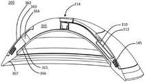
使用安装在眼睛上的显示器作为电子接触式镜片的示例来提供进一步的细节,但是应当理解,也可以制造其它类型的电子接触式镜片。图1A示出了佩戴安装在巩膜接触式镜片100中的显示器的用户。图1A还示出了与图2一起讨论的附件项链160。图1B示出了安装在用户眼睛上的巩膜接触式镜片100的截面视图。巩膜接触式镜片被设计成不在佩戴者的眼睛上来回移动。眼睛102包括角膜104和巩膜106。巩膜接触式镜片100由巩膜106和角膜104上方的拱顶支撑。泪液层108可以形成在接触式镜片100和角膜104之间。氧气透过接触式镜片100到达角膜104。Further details are provided using an eye-mounted display as an example of an electronic contact lens, but it should be understood that other types of electronic contact lenses can also be manufactured. FIG. 1A shows a user wearing a display mounted in a
接触式镜片100包含有效载荷。例如,有效载荷可以包括电子器件,该电子器件包括需要电源的电子器件,电源诸如电池或感应供电的线圈。在图1的示例中,有效载荷包括将图像投影到佩戴者的视网膜上的小型投影器(称为毫微微投影器114),以及操作毫微微投影器的相应电子器件112。这些由接收器线圈145供电,接收器线圈145围绕接触式镜片的周边定位。毫微微投影器114可以包括具有LED阵列的LED前板、具有接收数据以驱动LED前板的电子器件的ASIC背板、以及将来自LED阵列的光投影到视网膜上的光学器件。毫微微投影器114优选地适配于2mm×2mm×2mm的体积,或者甚至适配于1mm×1mm×1mm的体积。
毫微微投影器114定位在角膜上方,因为它将图像投影到视网膜上。电子器件112可以远离角膜定位,如图1B所示。为方便起见,接触式镜片100被分成中心区和周边区。中心区与角膜104重叠。角膜外的区域是周边区的一部分。在图1中,毫微微投影器114位于接触式镜片的中心区内,因为它将图像投射到用户的眼睛中,而电子器件112和线圈145位于周边区中。因为人们具有不同尺寸和形状的眼睛,为了方便起见,中心区可以被定义为接触式镜片的10mm直径的中心区域(即,在接触式镜片的中心轴线的5mm半径内)。角膜和巩膜之间的边界的直径通常为10-12.5mm。由于所需的光路,将光投射到视网膜上的有效载荷部件通常将位于中心区内。相反地,不将光投射到视网膜上或不以其他方式与视网膜相互作用的有效载荷部件可以位于中心区的边缘上或中心区的外部,使得它们不阻挡光到达视网膜。Femtoprojector 114 is positioned above the cornea as it projects the image onto the retina. The
供电有效载荷的其它示例包括传感器、成像器和眼睛跟踪部件,诸如加速计、陀螺仪和磁力计。有效载荷还可以包括无源器件,诸如用于无线电力或数据传输的线圈或天线,用于能量存储的电容器,以及无源光学结构(例如,吸收光的挡板、分束器、成像光学器件)。接触式镜片100还可以包含多个毫微微投影器,每个毫微微投影器将图像投影到用户的视网膜上。当用户的眼睛在其眼窝中旋转时,接触式镜片100随用户的眼睛102一起移动。因为毫微微投影器安装在接触式镜片100中,所以它们也随用户的眼睛移动并投影到视网膜的相同区域。一些毫微微投影器可以总是将图像投影到中央凹,而其它毫微微投影器可以总是将图像投影到具有较低分辨率的更多周边区。结果,不同的毫微微投影器可能具有不同的分辨率。来自不同毫微微投影器的图像可以重叠,以在佩戴者的视网膜上形成合成图像。Other examples of powered payloads include sensors, imagers, and eye-tracking components such as accelerometers, gyroscopes, and magnetometers. The payload may also include passive devices such as coils or antennas for wireless power or data transmission, capacitors for energy storage, and passive optical structures (eg, light-absorbing baffles, beam splitters, imaging optics ). The
关于接触式镜片,术语例如“顶部”,“前部”,“外部”和“前”是指远离佩戴者眼睛的方向,而“底部”,“后部”,“内部”和“后”是指朝向佩戴者眼睛的方向。With regard to contact lenses, terms such as "top", "front", "outer" and "front" refer to the direction away from the wearer's eye, while "bottom", "rear", "inner" and "rear" are Refers to the direction towards the wearer's eyes.
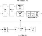
图2是使用上述巩膜接触式镜片的眼睛安装式显示器的功能框图。显示器可以分为数据/控制子系统200和电力子系统250。2 is a functional block diagram of an eye-mounted display using the scleral contact lens described above. The display can be divided into a data/control subsystem 200 and a power subsystem 250 .
在此示例中,数据/控制子系统200的接收路径包括天线210、接收器电路215、数据管线230和毫微微投影器240。来自外部源的数据以无线方式传输到显示器并经由天线210接收。接收器电路215执行用于接收数据的功能,例如解调、噪声滤波和放大。它还将接收到的信号转换成数字形式。管线230处理用于毫微微投影器240的数字信号。这些功能可以包括解码和定时。该处理还可以取决于在接触式镜片内部产生的其他信号,例如眼睛跟踪传感器220或环境光感测。然后,毫微微投影器240将相应的图像投影到佩戴者的视网膜上。在该示例中,毫微微投影器240包括CMOS ASIC背板242、LED前板244和光学器件246。In this example, the receive path of data/control subsystem 200 includes
数据/控制子系统200还可以包括通过发射器电路215和天线210的反向信道。例如,接触式镜片可以发送眼睛跟踪数据、控制数据和/或关于接触式镜片状态的数据。Data/control subsystem 200 may also include a reverse channel through
经由电力线圈260无线地接收电力。其耦合到调节和分配输入电力(例如,如果需要,从AC转换到DC)的电路270。电力子系统250还可以包括能量存储设备,例如电池265或电容器。Power is received wirelessly via the
除了图2所示的部件之外,整个系统还可以包括位于接触式镜片外部(即,镜片外)的部件。例如,头部跟踪和眼睛跟踪功能可以部分或全部在镜片外执行。数据管线也可以部分或全部在镜片外执行。图2的左手侧上的每个箭头也连接到镜片外部件。电力发射器线圈是镜片外的,用于接触式镜片显示器的图像数据和控制数据的源是镜片外的,并且反向信道的接收侧是镜片外的。In addition to the components shown in Figure 2, the overall system may include components that are external to the contact lens (ie, outside the lens). For example, head-tracking and eye-tracking functions can be performed partially or fully off-lens. The data pipeline can also be implemented partially or fully off-lens. Each arrow on the left hand side of Figure 2 is also connected to the outer lens component. The power transmitter coil is off-lens, the source of image data and control data for the contact lens display is off-lens, and the receive side of the reverse channel is off-lens.
有许多方式来实现不同的系统功能。系统的一些部分可以完全在用户的外部,而其他部分可以由用户以头戴式部件或眼镜的形式佩戴。例如,参见美国专利申请No.16/530,949,“Headgear Providing Inductive Coupling To A Contact Lens”(41898),其全部内容通过引用并入本文。部件也可以戴在皮带、臂带、腕带、项链或其它类型的包装上。图1A示出了在用户佩戴的项链160中实现某些功能的示例。在该示例中,项链160包括与眼睛安装式显示器100通信的无线发射器。There are many ways to implement different system functions. Some parts of the system may be entirely external to the user, while other parts may be worn by the user in the form of head-mounted components or glasses. See, eg, US Patent Application No. 16/530,949, "Headgear Providing Inductive Coupling To A Contact Lens" (41898), which is incorporated herein by reference in its entirety. Parts can also be worn on belts, armbands, wristbands, necklaces or other types of packaging. FIG. 1A shows an example of implementing certain functions in a
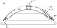
图3A和3B是包含具有非平面衬底的电子组件的电子接触式镜片100的截面图。巩膜接触式镜片100包括芯部305。芯部305具有安装至眼睛的巩膜上的基底表面307。芯部305还包含有效载荷。在该示例中,有效载荷包括图1中的毫微微投影器114和电子器件112(以及它们之间的互连)和线圈145以及其它部件。毫微微投影器114位于接触式镜片的中心区域,因为它将图像投影到用户的视网膜上。电子器件112和线圈145位于接触式镜片的周边,使得它们不阻挡进入用户眼睛的光。3A and 3B are cross-sectional views of an
电部件安装在非平面衬底310上,其定位部件并提供部件之间的电连接。非平面衬底310最初被制造成平面衬底,然后被弯曲成适配在接触式镜片内部的三维形状。三维形状包括承载电部件的平坦小面。电部件可以安装到衬底上,并在衬底仍然平坦时进行测试。例如,非平面衬底可以是柔性电路板,其还包含在部件之间提供电连接的导电迹线。在一些设计中,平坦小面被布置在带中。所述带中的相邻小面之间的弯曲形成所述三维形状。在弯曲之后,小面的带可以具有三维环形形状。包括衬底和部件的整个电子组件可以被封装在芯部305内。在图4-6中提供了进一步的描述。The electrical components are mounted on the
图3A至图3B还示出了允许用户角膜氧合的结构。接触式镜片100还包括透气外覆盖物362和透气内覆盖物366。每个覆盖物362,366在覆盖物和芯部305之间形成相应的空气间隙363,365。穿过芯部305的一个或多个空气轴364连接两个空气间隙363,365。这提供了氧气到达用户角膜的路径。例如,参见美国专利申请No.16/360,872,“Oxygen PermeableScleral Contact Lenses With Thick Payloads”(41902),其全部内容通过引用并入本文。Figures 3A-3B also illustrate structures that allow for oxygenation of the user's cornea.
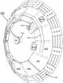
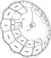
图4A和图4B是示出图3的电子组件的非平面衬底310和电部件的前立体视图和后立体视图。电子组件大致为穹顶形,以便适配到接触式镜片中。在图4A的前视图中,穹顶形组件的中心靠近观察者,而穹顶的周边远离观察者。当接触式镜片被佩戴时,图4A所示的表面背离佩戴者的眼睛。图4B的后视图示出了从穹顶内部观察的视图。穹顶的周边靠近观察者,而穹顶的中心远离观察者。图4B所示的表面面向佩戴者的眼睛。4A and 4B are front and rear perspective views illustrating the
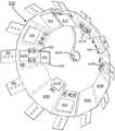
该特别的衬底310设计具有12个平坦的小面420A-L的带。该小面标记为A-L,其中小面420A位于带的一端,小面420L位于带的相对端。为了清楚起见,在每个图中没有标记每个小面。两个平面相交成一直线,因此相邻的小面420A和420B在可弯曲的边缘区域425处相交。小面420B和420C还在可弯曲边缘区域425处相交,等等。小面420L和420A不相交。在小面420L和420A之间存在间隙427,如图5所示。This
在该示例中,由十二个小面420形成的带是规则的12边截头锥体的一部分。具有小面的带是不透明的,但被定位成使得该带基本上不阻挡光通过接触式镜片进入眼睛。在该示例中,大多数半导体器件安装在每个小面的底部(后表面)上,如图4B所示。小面420可以具有不同的尺寸和/或形状以容纳不同的部件。在这些图中,可以使用柱面坐标系来描述位置。“高度”或“z”是指沿着接触式镜片的中心轴的方向。“半径”或“r”是指从中心轴线向外的径向方向。由于接触式镜片的形状、半径和高度不是独立的。“方位角”或“弧”或“θ”是垂直于z方向的平面中的角方向。In this example, the band formed by twelve facets 420 is part of a regular 12-sided frustum. The faceted band is opaque, but is positioned such that the band does not substantially block light from entering the eye through the contact lens. In this example, most of the semiconductor devices are mounted on the bottom (back surface) of each facet, as shown in Figure 4B. Facets 420 may have different sizes and/or shapes to accommodate different components. In these figures, a cylindrical coordinate system can be used to describe the position. "Height" or "z" refers to the direction along the central axis of the contact lens. "Radius" or "r" refers to the radial direction outward from the central axis. Since the shape, radius and height of contact lenses are not independent. An "azimuth" or "arc" or "theta" is an angular direction in a plane perpendicular to the z-direction.
在图4B的示例中,部件包括用于眼睛跟踪的三个磁力计416和四个加速计417A-B。这些传感器芯片彼此以特定角度安装,以允许沿线性独立的空间轴进行感测。例如,参见美国专利申请No.16/005,379,“Contact Lens-Based Eye Tracking”(38838),其全部内容通过引用并入本文。十二个小面基本上形成完整的环形,因此每个小面对着360/12=30度的弧。利用这种布局,放置在每隔两个小面的小面上的四个元件间隔90度,放置在每隔三个小面的小面上的三个元件间隔120度。磁力计416安装在每隔3个小面的小面上,即420D,420H和420L上,使得它们间隔120度,并且它们都与接触式镜片的中心相距大致相同的径向距离。In the example of Figure 4B, the components include three
有两对加速度计417A和417B。一对加速度计417A安装在径向相对的小面420E和420K上,以便增加它们之间的距离。类似地,另一对417B安装在径向相对的小面420C和420I上。在这种配置中,两对加速度计没有间隔90度,但是没有两个加速度计安装在相邻的小面上。在可替换的设计中,代替所示的配置,加速度计可以安装在每隔两个小面的小面上。径向方向而言,一对417B安装在朝向具有小面的带的周边的更大的半径处,而一对417A安装在更朝向带的中心的位置处,以便增加两对之间的垂直间隔。实际上,小面420E和420K朝向中心延伸以增加该间隔。如果需要额外的延伸,可以引入额外的弯曲以与接触式镜片的形状保形。参见下面的小面420I的讨论。There are two pairs of
图4B的电子组件还包括用于毫微微投影器的半导体器件414。图4B中未示出毫微微投影器的光学器件,但是器件414包括用于毫微微投影器的ASIC背板和LED前板。例如,参见美国专利申请No.16/034,761,“Advanced Optical Designs for Eye-Mounted ImagingSystems,”(40785);15/892,891,“Backplane for Eye-Mounted Display,”(37916);和16/154,603,“Ultra-Dense LED Projector Using Thinned Gallium Nitride,”(40231),其全部内容通过引用并入本文。毫微微投影器位于接触式镜片的中心,因此衬底具有从具有小面420的主带延伸到承载毫微微投影器器件414的岛部424的窄桥部423。因为衬底是柔性的,桥部423可以被弯曲以与接触式镜片的形状保形。如图4B所示,岛部424具有孔424X。LED前板位于岛部424的一侧,而毫微微投影器光学器件位于岛部424的另一侧。孔424X允许来自LED前板的光进入毫微微投影器器件的光学器件。The electronic assembly of FIG. 4B also includes a
该示例还包括面向外侧的成像器,其安装在延伸接片429上。例如,参见美国专利申请No.15/886,398,“Eye-Mounted Device Including a Femtocamera andFemtoprojector,”(37924),其全部内容通过引用并入本文。半导体器件419是用于成像器(诸如检测器阵列)和处理的电子器件。如果将成像器直接安装在现有的小面420I上,则它将离轴倾斜太远,而如果定位得离周边太远,则还可能被用户的眼睑阻挡。结果,小面420I被缩短(其内边缘相对于其它小面偏移),且平坦延伸接片429从小面420I径向延伸。在边缘区域428处的弯曲允许接片429以与主小面420不同的角度倾斜,使得成像器的视场更多在轴上。成像器光学器件在衬底429的一侧上,而电子器件419在另一侧上,其中孔429X在两者之间。This example also includes an outboard facing imager mounted on
该示例中的电子组件还包括处理器412和RF滤波器413。衬底还包括平坦的延伸接片445以承载线圈145。这些接片445从主小面420径向延伸,它们间具有弯曲。这些孔允许浇铸树脂流过柔性电路板并围绕线圈线流动。The electronic components in this example also include a
图4示出了折叠成形后的电子组件。图5是电子组件在折叠之前的后视图。衬底310是柔性平坦电路板。电路板可仅在一侧上具有导电迹线。可替换地,它可以具有非导电芯部,在芯部的两侧上具有导电迹线,以及在芯部的两侧之间具有通孔。它也可以是多层板。在弯曲之后将保持平坦的区域的大致边界由虚线示出。Figure 4 shows the electronic assembly after being folded into shape. Figure 5 is a rear view of the electronic assembly prior to folding. The
衬底最初被制成平坦的。部件可以被放置在衬底上、键合到衬底上,并且当组件是平坦时进行电测试。可使用常规技术(例如表面式安装或倒装芯片式安装)将半导体器件安装在平坦小面上。各向异性导电胶(ACP)也可用于将半导体器件附接到衬底上。部件可安装在小面的任一侧或两侧。可替换地,小面可以包含一个切口,该部件位于该切口中。这样,总厚度仅仅是元件的厚度,而不是部件的厚度加上衬底的厚度。在一种方法中,这些部件沿一个边缘倒装接合,而其余边缘用ACP粘合,以稳定部件在切口中的位置。The substrate is initially made flat. Components can be placed on a substrate, bonded to the substrate, and electrically tested when the assembly is flat. Semiconductor devices can be mounted on flat facets using conventional techniques such as surface mounting or flip-chip mounting. Anisotropic conductive pastes (ACPs) can also be used to attach semiconductor devices to substrates. Components can be mounted on either or both sides of the facet. Alternatively, the facet may contain a cutout in which the component is located. Thus, the total thickness is simply the thickness of the component, not the thickness of the component plus the thickness of the substrate. In one approach, the parts are flip-chip bonded along one edge, while the remaining edges are bonded with ACP to stabilize the part's position in the cutout.
图6A和图6B是示出具有线圈和包覆成型件的图3的电子组件的前立体视图和后立体视图。这里,与图4相比,毫微微投影器光学器件614和成像器光学器件619已经安装到衬底上。线圈145也被安装到衬底上。6A and 6B are front and rear perspective views showing the electronic assembly of FIG. 3 with a coil and an overmold. Here, in contrast to Figure 4,
如在图6B中更清楚地看到的,包覆成型件610A-L也被添加到小面。在将部件安装在图5的平坦衬底上之后,用聚合物包覆模制小面420。可以将聚合物设计成具有特定的刚度、尺寸稳定性、粘合性和/或防潮密封性能。包覆成型增加了承载电部件的平坦小面的刚度。然后,将电子组件折叠成圆锥形状以适配在接触式镜片内。As seen more clearly in Figure 6B, overmolds 610A-L are also added to the facets. After mounting the components on the flat substrate of FIG. 5, facet 420 is overmolded with polymer. The polymers can be designed to have specific stiffness, dimensional stability, adhesion and/or moisture sealing properties. Overmolding increases the stiffness of the flat facets that carry the electrical components. The electronic assembly is then folded into a conical shape to fit within the contact lens.
聚合物包覆成型件610确保每个小面保持平坦并且与周围环境隔离。从芯片到总线的所有键合都在平坦部分上,并且它们被保护免受机械应力。该包覆成型件610封装安装在小面420上的电部件。它保护部件。它还增加了平坦小面的刚度,以进一步防止平坦小面的不希望的弯曲,特别是在安装电部件的位置。也可以使用其它类型的加强件。图6A还示出了天线620。可替换地,天线可以实现为电路板上的导电图案。The polymer overmold 610 ensures that each facet remains flat and isolated from the surrounding environment. All the bonds from chip to bus are on flat sections and they are protected from mechanical stress. The overmold 610 encapsulates the electrical components mounted on the facet 420 . It protects the parts. It also increases the stiffness of the flat facet to further prevent undesired bending of the flat facet, especially where electrical components are mounted. Other types of reinforcements can also be used. FIG. 6A also shows
电部件的面向外的(前)表面可以被着色以匹配人眼的颜色和标记,由此使得接触式镜片在佩戴时看起来更自然。The outward-facing (front) surface of the electrical component can be tinted to match the color and markings of the human eye, thereby making the contact lens look more natural when worn.
图4至图6示出了一个示例。其它变化将是显而易见的。例如,每个小面可以具有与所有其它小面相同的尺寸和形状,或者一些小面可以具有与其它小面不同的尺寸和形状,或者所有小面可以具有不同的尺寸和形状。每个小面的内边缘和外边缘与接触式镜片的中心的距离可以不同。电部件可以安装在小面的前侧、后侧或两侧上。4 to 6 show an example. Other changes will be apparent. For example, each facet can have the same size and shape as all other facets, or some facets can have a different size and shape than others, or all facets can have a different size and shape. The inner and outer edges of each facet can be at different distances from the center of the contact lens. Electrical components can be mounted on the front, rear or both sides of the facet.
小面的倾斜角和它们的尺寸可以被调节以在接触式镜片的范围内容纳不同尺寸的部件。小面可以被布置成在衬底被折叠成其三维形状之后相对于彼此或相对于接触式镜片成特定角度。例如,在一种设计中,当衬底被折叠成其最终形状时,在方位角上间隔120度的三个小面位于相互垂直的定向上。这种类型的配置对于眼睛跟踪是有用的。The angle of inclination of the facets and their dimensions can be adjusted to accommodate different sized components within the confines of a contact lens. The facets may be arranged at specific angles relative to each other or relative to the contact lens after the substrate is folded into its three-dimensional shape. For example, in one design, when the substrate is folded into its final shape, three facets spaced 120 degrees apart in azimuth are in mutually perpendicular orientations. This type of configuration is useful for eye tracking.
小面可以基于不规则的截头锥体。可替换,它们可以基于多个截头锥体。例如,小平面可以在两个不同的倾斜角之间交替。奇数小面可以基于具有较陡边的截头锥体,而偶数小面可以基于具有较不陡边的截头锥体。相邻的小面仍然在边缘区域相交,但是边缘可能相对于接触式镜片的中心轴偏斜,并且奇数和偶数小面可能具有不同的形状。不同的部件可能对它们在接触式镜片内的位置或它们相对于接触式镜片中心轴线的倾斜角具有不同的要求。小面可以被设计成满足这些要求。部件也可以具有不同的尺寸和形状。一些小平面可以更大以容纳更大的部件。Facets can be based on irregular frustums. Alternatively, they can be based on multiple frustums. For example, the facets can alternate between two different tilt angles. The odd-numbered facets may be based on frustums with steeper sides, while the even-numbered facets may be based on frustums with less steep sides. Adjacent facets still meet at the edge region, but the edges may be skewed relative to the central axis of the contact lens, and odd and even facets may have different shapes. Different components may have different requirements for their position within the contact lens or their angle of inclination relative to the central axis of the contact lens. Facets can be designed to meet these requirements. Components can also have different sizes and shapes. Some facets can be larger to accommodate larger components.
具有小面的带也可以具有不同的设计。它不必覆盖整个360度的弧。它可以成形为实质地小于完全的环。在图4至图6中,小面420A-B不承载除线圈之外的任何电部件。如果以某种其它方式支撑线圈145,则可以省略它们。可以有多个带。带的宽度可以更窄或更宽或更不均匀。不同的小面也可以具有不同的宽度。Bands with facets can also have different designs. It doesn't have to cover the entire 360 degree arc. It can be shaped to be substantially smaller than a complete ring. In Figures 4-6,
图7A和图7B是示出另一电子组件的前立体视图和后立体视图。在该示例中,非平面衬底710包括具有十二个平坦小面720A-L的带。如图7B所示,许多这些小面承载有电池747。延伸接片729朝向接触式镜片的中心延伸。这些延伸接片729承载许多由图4至图6中的主小面承载的电部件。图7中用4xx数字标记的电部件与图4中的相同。与图6相比,图7中的设计具有更大的中心开口,这可以允许更好的周边视觉。7A and 7B are a front perspective view and a rear perspective view showing another electronic component. In this example, the
图8是示出了具有包覆成型件的图7的电子组件的后立体视图。已经添加了毫微微投影器光学器件614和成像器光学器件619。半导体器件已经被包覆成型810。8 is a rear perspective view showing the electronic assembly of FIG. 7 with an overmold.
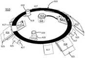
图9A是示出又一电子组件的前立体视图。图9B是电子组件的局部剖视图。在该设计中,非平面衬底910具有平坦的环形芯部部分920。平坦接片925从环形芯部920径向延伸,并且电部件安装在这些接片925上。在一种方法中,接片925和芯部920在可弯曲的边缘区域相交。因此,整个衬底910可以被制造成平坦的,包括提供到电部件的电连接的导电迹线。部件可以被放置在衬底上,键合到衬底上,并且当组件是平坦时进行电测试。可以添加光学器件和包覆成型件。然后可以将整个组件折叠成三维形状以适配到接触式镜片中。9A is a front perspective view showing yet another electronic assembly. 9B is a partial cross-sectional view of the electronic assembly. In this design, the
该示例示出了可以具有与先前示例相同的部件。它包括毫微微电子器件414和光学器件614、以及成像器电子器件419和光学器件619。它还包括磁力计416和加速计417、处理器412和RF滤波器413。附加的接片(未示出)可用于承载线圈或电池。This example shows that it is possible to have the same components as the previous example. It includes
在可替换的方法中,接片925可以是与芯部920分离的片,并且随后附接到芯部920。In an alternative approach, the
尽管具体实施方式部分包含许多细节,但是这些细节不应当被解释为限制本发明的范围,而仅仅是说明不同的示例。应当理解,本公开的范围包括上面未详细讨论的其它实施例。在不脱离所附权利要求所限定的精神和范围的情况下,可以对在此公开的方法和装置的布置、操作和细节进行对本领域技术人员显而易见的各种其它修改、改变和变化。因此,本发明的范围应当由所附权利要求及其法律等同物来确定。Although the Detailed Description section contains numerous details, these should not be construed as limiting the scope of the invention, but merely as illustrating different examples. It should be understood that the scope of the present disclosure includes other embodiments not discussed in detail above. Various other modifications, changes and variations apparent to those skilled in the art may be made in the arrangement, operation and details of the methods and apparatus disclosed herein without departing from the spirit and scope as defined by the appended claims. Accordingly, the scope of the invention should be determined by the appended claims and their legal equivalents.
Claims (22)
Translated fromChineseApplications Claiming Priority (3)
| Application Number | Priority Date | Filing Date | Title |
|---|---|---|---|
| US16/554,399 | 2019-08-28 | ||
| US16/554,399US11237410B2 (en) | 2019-08-28 | 2019-08-28 | Electronics assembly for use in electronic contact lens |
| PCT/US2020/048286WO2021041737A1 (en) | 2019-08-28 | 2020-08-27 | Electronics assembly for use in electronic contact lens |
Publications (1)
| Publication Number | Publication Date |
|---|---|
| CN114631048Atrue CN114631048A (en) | 2022-06-14 |
Family
ID=74682255
Family Applications (1)
| Application Number | Title | Priority Date | Filing Date |
|---|---|---|---|
| CN202080074199.6APendingCN114631048A (en) | 2019-08-28 | 2020-08-27 | Electronic assembly for use within an electronic contact lens |
Country Status (4)
| Country | Link |
|---|---|
| US (2) | US11237410B2 (en) |
| EP (1) | EP4018255B1 (en) |
| CN (1) | CN114631048A (en) |
| WO (1) | WO2021041737A1 (en) |
Families Citing this family (7)
| Publication number | Priority date | Publication date | Assignee | Title |
|---|---|---|---|---|
| SG11202011022VA (en) | 2018-05-10 | 2020-12-30 | Acucela Inc | Method and apparatus for treating refractive error of the eye |
| AU2019314262B2 (en) | 2018-07-30 | 2025-04-03 | Acucela Inc. | An apparatus to treat myopia of an eye |
| WO2021022193A1 (en) | 2019-07-31 | 2021-02-04 | Acucela Inc. | Device for projecting images on the retina |
| US11209672B1 (en) | 2021-04-06 | 2021-12-28 | Acucela Inc. | Supporting pillars for encapsulating a flexible PCB within a soft hydrogel contact lens |
| US11366341B1 (en) | 2021-05-04 | 2022-06-21 | Acucela Inc. | Electronic case for electronic spectacles |
| CN117215087A (en)* | 2022-06-12 | 2023-12-12 | 晶硕光学股份有限公司 | Contact lens |
| US20240168312A1 (en)* | 2022-11-18 | 2024-05-23 | Tectus Corporation | Electronic contact lens pair symmetry |
Citations (7)
| Publication number | Priority date | Publication date | Assignee | Title |
|---|---|---|---|---|
| CN103135252A (en)* | 2011-11-30 | 2013-06-05 | 庄臣及庄臣视力保护公司 | Electrical interconnects in an electronic contact lens |
| CN105988230A (en)* | 2015-03-19 | 2016-10-05 | 庄臣及庄臣视力保护公司 | Thinned and flexible circuit boards on three-dimensional surfaces |
| CN106415373A (en)* | 2014-06-13 | 2017-02-15 | 威里利生命科学有限责任公司 | Flexible conductor for use within a contact lens |
| CN108604044A (en)* | 2016-03-14 | 2018-09-28 | 弗劳恩霍夫应用研究促进协会 | Multi-aperture imaging device, imaging system and method for detecting target area |
| US20190094981A1 (en)* | 2014-06-14 | 2019-03-28 | Magic Leap, Inc. | Methods and systems for creating virtual and augmented reality |
| US20190243130A1 (en)* | 2018-02-07 | 2019-08-08 | Lockheed Martin Corporation | Plenoptic Cellular Vision Correction |
| CN111201468A (en)* | 2017-10-11 | 2020-05-26 | 威里利生命科学有限责任公司 | Voltage driver for electrowetting lens |
Family Cites Families (25)
| Publication number | Priority date | Publication date | Assignee | Title |
|---|---|---|---|---|
| US5682210A (en) | 1995-12-08 | 1997-10-28 | Weirich; John | Eye contact lens video display system |
| US6544193B2 (en)* | 1996-09-04 | 2003-04-08 | Marcio Marc Abreu | Noninvasive measurement of chemical substances |
| US8446341B2 (en)* | 2007-03-07 | 2013-05-21 | University Of Washington | Contact lens with integrated light-emitting component |
| WO2008109867A2 (en) | 2007-03-07 | 2008-09-12 | University Of Washington | Active contact lens |
| US8786675B2 (en) | 2008-01-23 | 2014-07-22 | Michael F. Deering | Systems using eye mounted displays |
| JP2011515157A (en) | 2008-03-18 | 2011-05-19 | ピクセルオプティクス, インコーポレイテッド | Advanced electroactive optical component devices |
| US8154804B2 (en) | 2008-03-25 | 2012-04-10 | E-Vision Smart Optics, Inc. | Electro-optic lenses for correction of higher order aberrations |
| US20100076553A1 (en) | 2008-09-22 | 2010-03-25 | Pugh Randall B | Energized ophthalmic lens |
| BR112012016419B1 (en) | 2010-01-05 | 2020-12-29 | Sensimed Sa | intraocular pressure monitoring device, kit and intraocular pressure monitoring system |
| US8857983B2 (en)* | 2012-01-26 | 2014-10-14 | Johnson & Johnson Vision Care, Inc. | Ophthalmic lens assembly having an integrated antenna structure |
| US9351827B2 (en) | 2012-04-03 | 2016-05-31 | Johnson & Johnson Vision Care, Inc. | Lens driver for variable-optic electronic ophthalmic lens |
| US20140000101A1 (en) | 2012-06-29 | 2014-01-02 | Johnson & Johnson Vision Care, Inc. | Methods and apparatus to form printed batteries on ophthalmic devices |
| US8894201B2 (en) | 2013-03-15 | 2014-11-25 | Johnson & Johnson Vision Care, Inc. | Methods and ophthalmic devices with thin film transistors |
| US9113829B2 (en) | 2013-03-27 | 2015-08-25 | Google Inc. | Systems and methods for encapsulating electronics in a mountable device |
| US9977256B2 (en)* | 2013-05-30 | 2018-05-22 | Johnson & Johnson Vision Care, Inc. | Methods for manufacturing and programming an energizable ophthalmic lens with a programmable media insert |
| US20200119316A9 (en) | 2014-07-21 | 2020-04-16 | Johnson & Johnson Vision Care, Inc. | Flexible micro-battery |
| EP3241062A1 (en)* | 2014-08-05 | 2017-11-08 | EP Global Communications Inc. | Electronic medical devices and methods |
| KR102248847B1 (en)* | 2015-06-01 | 2021-05-06 | 삼성전자주식회사 | Contact lens with an energy harvesting unit |
| US10678068B2 (en) | 2015-12-18 | 2020-06-09 | Verily Life Sciences Llc | Electrochromic contact lens |
| US10353463B2 (en) | 2016-03-16 | 2019-07-16 | RaayonNova LLC | Smart contact lens with eye driven control system and method |
| US20180104921A1 (en) | 2016-10-17 | 2018-04-19 | Johnson & Johnson Vision Care, Inc. | Biomedical device batteries with electrodeposited cathodes |
| US20180115017A1 (en) | 2016-10-20 | 2018-04-26 | Johnson & Johnson Vision Care, Inc. | Biomedical energization elements with polymer electrolytes |
| JP6174232B1 (en) | 2016-11-25 | 2017-08-02 | 株式会社ユニバーサルビュー | Pinhole contact lens and smart contact system |
| US10129984B1 (en)* | 2018-02-07 | 2018-11-13 | Lockheed Martin Corporation | Three-dimensional electronics distribution by geodesic faceting |
| US11681164B2 (en)* | 2018-07-27 | 2023-06-20 | Tectus Corporation | Electrical interconnects within electronic contact lenses |
- 2019
- 2019-08-28USUS16/554,399patent/US11237410B2/enactiveActive
- 2020
- 2020-08-27CNCN202080074199.6Apatent/CN114631048A/enactivePending
- 2020-08-27WOPCT/US2020/048286patent/WO2021041737A1/ennot_activeCeased
- 2020-08-27EPEP20856717.2Apatent/EP4018255B1/enactiveActive
- 2022
- 2022-01-06USUS17/570,307patent/US11656483B2/enactiveActive
Patent Citations (8)
| Publication number | Priority date | Publication date | Assignee | Title |
|---|---|---|---|---|
| CN103135252A (en)* | 2011-11-30 | 2013-06-05 | 庄臣及庄臣视力保护公司 | Electrical interconnects in an electronic contact lens |
| CN106415373A (en)* | 2014-06-13 | 2017-02-15 | 威里利生命科学有限责任公司 | Flexible conductor for use within a contact lens |
| US20190094981A1 (en)* | 2014-06-14 | 2019-03-28 | Magic Leap, Inc. | Methods and systems for creating virtual and augmented reality |
| CN105988230A (en)* | 2015-03-19 | 2016-10-05 | 庄臣及庄臣视力保护公司 | Thinned and flexible circuit boards on three-dimensional surfaces |
| CN108604044A (en)* | 2016-03-14 | 2018-09-28 | 弗劳恩霍夫应用研究促进协会 | Multi-aperture imaging device, imaging system and method for detecting target area |
| US20190011809A1 (en)* | 2016-03-14 | 2019-01-10 | Fraunhofer-Gesellschaft Zur Foerderung Der Angewandten Forschung E.V. | Multi-aperture imaging device, imaging system and method for capturing an object area |
| CN111201468A (en)* | 2017-10-11 | 2020-05-26 | 威里利生命科学有限责任公司 | Voltage driver for electrowetting lens |
| US20190243130A1 (en)* | 2018-02-07 | 2019-08-08 | Lockheed Martin Corporation | Plenoptic Cellular Vision Correction |
Also Published As
| Publication number | Publication date |
|---|---|
| EP4018255B1 (en) | 2025-02-12 |
| US20220128842A1 (en) | 2022-04-28 |
| EP4018255A4 (en) | 2023-09-13 |
| WO2021041737A1 (en) | 2021-03-04 |
| US11237410B2 (en) | 2022-02-01 |
| US11656483B2 (en) | 2023-05-23 |
| EP4018255A1 (en) | 2022-06-29 |
| US20210063773A1 (en) | 2021-03-04 |
Similar Documents
| Publication | Publication Date | Title |
|---|---|---|
| US11656483B2 (en) | Electronics assembly for use in electronic contact lens | |
| US12206250B2 (en) | NFC communication and QI wireless charging of eyewear | |
| US12219234B2 (en) | Wearable electronic device including small camera | |
| CN116601543A (en) | System with display and sensor | |
| JP2020532895A (en) | Audio output assembly for head-mounted displays | |
| JP7332680B2 (en) | Mesa formation for wafer-to-wafer bonding | |
| CN115803676A (en) | Detachable camera module for wearable device | |
| US10070028B2 (en) | Optical systems and methods of use | |
| CN116325709A (en) | Electronic device including camera module | |
| CN117083541A (en) | Projector with field lens | |
| WO2023009310A1 (en) | Eyewear with slot-ring antenna | |
| JP2022142915A (en) | Filming device and helmet with filming device | |
| US20240295759A1 (en) | Eye tracking glasses | |
| KR20220104576A (en) | Wearable electronic device including small camera | |
| TW201516466A (en) | Head-mounted display | |
| US20240168312A1 (en) | Electronic contact lens pair symmetry | |
| EP4586409A2 (en) | Eyewear with aperture tuned dielectric loaded multi-band antenna | |
| CN119213353A (en) | Goggles with shape memory alloy actuators | |
| CN118891562A (en) | Goggles with RF shield having grounding spring | |
| US20240160042A1 (en) | Oxygen permeable electronic contact lenses fabricated using a solidification process | |
| US20240274587A1 (en) | 3d chiplet integration using fan-out wafer-level packaging | |
| KR20250047060A (en) | Wearable device including heat dissipation structure | |
| CN118785603A (en) | Electronic Devices | |
| JP2005134825A (en) | Optical element assembly and imaging apparatus equipped with the same |
Legal Events
| Date | Code | Title | Description |
|---|---|---|---|
| PB01 | Publication | ||
| PB01 | Publication | ||
| SE01 | Entry into force of request for substantive examination | ||
| SE01 | Entry into force of request for substantive examination | ||
| WD01 | Invention patent application deemed withdrawn after publication | Application publication date:20220614 | |
| WD01 | Invention patent application deemed withdrawn after publication |