CN114616732A - Laser diode driving circuit - Google Patents
Laser diode driving circuitDownload PDFInfo
- Publication number
- CN114616732A CN114616732ACN202080074065.4ACN202080074065ACN114616732ACN 114616732 ACN114616732 ACN 114616732ACN 202080074065 ACN202080074065 ACN 202080074065ACN 114616732 ACN114616732 ACN 114616732A
- Authority
- CN
- China
- Prior art keywords
- laser diode
- switching element
- circuit
- laser
- capacitor
- Prior art date
- Legal status (The legal status is an assumption and is not a legal conclusion. Google has not performed a legal analysis and makes no representation as to the accuracy of the status listed.)
- Pending
Links
Images


Classifications
- H—ELECTRICITY
- H01—ELECTRIC ELEMENTS
- H01S—DEVICES USING THE PROCESS OF LIGHT AMPLIFICATION BY STIMULATED EMISSION OF RADIATION [LASER] TO AMPLIFY OR GENERATE LIGHT; DEVICES USING STIMULATED EMISSION OF ELECTROMAGNETIC RADIATION IN WAVE RANGES OTHER THAN OPTICAL
- H01S5/00—Semiconductor lasers
- H01S5/04—Processes or apparatus for excitation, e.g. pumping, e.g. by electron beams
- H01S5/042—Electrical excitation ; Circuits therefor
- H01S5/0428—Electrical excitation ; Circuits therefor for applying pulses to the laser
- G—PHYSICS
- G01—MEASURING; TESTING
- G01S—RADIO DIRECTION-FINDING; RADIO NAVIGATION; DETERMINING DISTANCE OR VELOCITY BY USE OF RADIO WAVES; LOCATING OR PRESENCE-DETECTING BY USE OF THE REFLECTION OR RERADIATION OF RADIO WAVES; ANALOGOUS ARRANGEMENTS USING OTHER WAVES
- G01S17/00—Systems using the reflection or reradiation of electromagnetic waves other than radio waves, e.g. lidar systems
- G01S17/02—Systems using the reflection of electromagnetic waves other than radio waves
- G01S17/06—Systems determining position data of a target
- G01S17/42—Simultaneous measurement of distance and other co-ordinates
- G—PHYSICS
- G01—MEASURING; TESTING
- G01S—RADIO DIRECTION-FINDING; RADIO NAVIGATION; DETERMINING DISTANCE OR VELOCITY BY USE OF RADIO WAVES; LOCATING OR PRESENCE-DETECTING BY USE OF THE REFLECTION OR RERADIATION OF RADIO WAVES; ANALOGOUS ARRANGEMENTS USING OTHER WAVES
- G01S17/00—Systems using the reflection or reradiation of electromagnetic waves other than radio waves, e.g. lidar systems
- G01S17/88—Lidar systems specially adapted for specific applications
- G01S17/93—Lidar systems specially adapted for specific applications for anti-collision purposes
- G01S17/931—Lidar systems specially adapted for specific applications for anti-collision purposes of land vehicles
- G—PHYSICS
- G01—MEASURING; TESTING
- G01S—RADIO DIRECTION-FINDING; RADIO NAVIGATION; DETERMINING DISTANCE OR VELOCITY BY USE OF RADIO WAVES; LOCATING OR PRESENCE-DETECTING BY USE OF THE REFLECTION OR RERADIATION OF RADIO WAVES; ANALOGOUS ARRANGEMENTS USING OTHER WAVES
- G01S7/00—Details of systems according to groups G01S13/00, G01S15/00, G01S17/00
- G01S7/48—Details of systems according to groups G01S13/00, G01S15/00, G01S17/00 of systems according to group G01S17/00
- G01S7/481—Constructional features, e.g. arrangements of optical elements
- G01S7/4814—Constructional features, e.g. arrangements of optical elements of transmitters alone
- G—PHYSICS
- G01—MEASURING; TESTING
- G01S—RADIO DIRECTION-FINDING; RADIO NAVIGATION; DETERMINING DISTANCE OR VELOCITY BY USE OF RADIO WAVES; LOCATING OR PRESENCE-DETECTING BY USE OF THE REFLECTION OR RERADIATION OF RADIO WAVES; ANALOGOUS ARRANGEMENTS USING OTHER WAVES
- G01S7/00—Details of systems according to groups G01S13/00, G01S15/00, G01S17/00
- G01S7/48—Details of systems according to groups G01S13/00, G01S15/00, G01S17/00 of systems according to group G01S17/00
- G01S7/483—Details of pulse systems
- G01S7/484—Transmitters
- H—ELECTRICITY
- H01—ELECTRIC ELEMENTS
- H01S—DEVICES USING THE PROCESS OF LIGHT AMPLIFICATION BY STIMULATED EMISSION OF RADIATION [LASER] TO AMPLIFY OR GENERATE LIGHT; DEVICES USING STIMULATED EMISSION OF ELECTROMAGNETIC RADIATION IN WAVE RANGES OTHER THAN OPTICAL
- H01S5/00—Semiconductor lasers
- H01S5/02—Structural details or components not essential to laser action
- H01S5/022—Mountings; Housings
- H01S5/0233—Mounting configuration of laser chips
- H—ELECTRICITY
- H01—ELECTRIC ELEMENTS
- H01S—DEVICES USING THE PROCESS OF LIGHT AMPLIFICATION BY STIMULATED EMISSION OF RADIATION [LASER] TO AMPLIFY OR GENERATE LIGHT; DEVICES USING STIMULATED EMISSION OF ELECTROMAGNETIC RADIATION IN WAVE RANGES OTHER THAN OPTICAL
- H01S5/00—Semiconductor lasers
- H01S5/06—Arrangements for controlling the laser output parameters, e.g. by operating on the active medium
- H01S5/062—Arrangements for controlling the laser output parameters, e.g. by operating on the active medium by varying the potential of the electrodes
- H01S5/06209—Arrangements for controlling the laser output parameters, e.g. by operating on the active medium by varying the potential of the electrodes in single-section lasers
- H01S5/06216—Pulse modulation or generation
Landscapes
- Physics & Mathematics (AREA)
- Engineering & Computer Science (AREA)
- General Physics & Mathematics (AREA)
- Electromagnetism (AREA)
- Computer Networks & Wireless Communication (AREA)
- Radar, Positioning & Navigation (AREA)
- Remote Sensing (AREA)
- Condensed Matter Physics & Semiconductors (AREA)
- Optics & Photonics (AREA)
- Semiconductor Lasers (AREA)
Abstract
Description
Translated fromChinese技术领域technical field
本发明涉及一种激光二极管驱动电路。The invention relates to a laser diode driving circuit.
背景技术Background technique
专利文献1公开了一种能够输出短脉冲的激光的激光二极管驱动电路。该激光二极管驱动电路关断开关元件以对电容器进行充电,然后导通开关元件以利用电容器的放电电流使激光二极管发光,并且在激光二极管停止发光后关断开关元件以再次对电容器进行充电(参见专利文献1的图2)。
现有技术文献prior art literature
专利文献Patent Literature
专利文献1:日本特开2016-152336号公报Patent Document 1: Japanese Patent Laid-Open No. 2016-152336
发明内容SUMMARY OF THE INVENTION
发明要解决的问题Invention to solve problem
根据专利文献1,当电容器中蓄积的电荷耗尽时,电容器的放电电流变为零,激光二极管停止发光。这里,从开关元件导通到电容器的放电电流变为零的时段,即激光的脉冲宽度依赖于LCR谐振电路的电路常数。LCR谐振电路包括电容器、激光二极管、处于导通状态的开关元件、以阳极和阴极相对于激光二极管的阳极和阴极反向的方式与所述激光二极管并联连接的二极管、以及寄生电感。According to
在专利文献1中公开的激光二极管驱动电路中,开关元件的导通时段被设定为激光的输出时段的1000倍以上(参见专利文献1的段落0042至0043、以及图3和图6)。这会导致间歇地输出不必要的激光,直到LCR谐振电路的谐振充分衰减。In the laser diode drive circuit disclosed in
本发明的目的在于,提供一种能够抑制不必要的激光输出的激光二极管驱动电路、以及包括这种激光二极管驱动电路的激光装置、激光雷达装置及车辆。An object of the present invention is to provide a laser diode drive circuit capable of suppressing unnecessary laser output, and a laser device, a laser radar device, and a vehicle including such a laser diode drive circuit.
解决问题的手段means of solving problems
为了实现上述目的,根据本发明的一方面,一种激光二极管驱动电路,包括:开关元件;控制器,其被配置为导通和关断所述开关元件;第二串联电路,其与包括激光二极管的第一串联电路并联连接;以及电容器。所述第二串联电路包括整流元件、以及被配置为限制流过所述整流元件的电流的电流限制器,并且以使所述整流元件的阳极指向阴极的方向与所述激光二极管的阳极指向阴极的方向相反的方式与所述第一串联电路并联连接。所述电容器被配置为在所述开关元件关断时被充电,并且在所述开关元件导通时与所述开关元件、所述第一串联电路及所述第二串联电路形成闭合电路(第一配置)。作为所述电容器,可以仅设置一个电容器,或者也可以设置并联连接的多个电容器。In order to achieve the above object, according to an aspect of the present invention, a laser diode driving circuit includes: a switching element; a controller configured to turn on and off the switching element; a first series circuit of diodes connected in parallel; and a capacitor. The second series circuit includes a rectifying element, and a current limiter configured to limit the current flowing through the rectifying element in a direction such that the anode of the rectifying element points to the cathode and the anode of the laser diode points to the cathode is connected in parallel with the first series circuit in the opposite direction. The capacitor is configured to be charged when the switching element is turned off, and to form a closed circuit with the switching element, the first series circuit, and the second series circuit when the switching element is turned on (No. a configuration). As the capacitor, only one capacitor may be provided, or a plurality of capacitors connected in parallel may be provided.
所述第一串联电路可以只包括所述激光二极管,或者可以串联连接有包括所述激光二极管的多个构件。多个构件中的至少一个可以是并联电路。The first series circuit may include only the laser diode, or a plurality of components including the laser diode may be connected in series. At least one of the plurality of components may be a parallel circuit.
优选地,上述第一配置的激光二极管驱动电路还包括被配置为检测流过所述激光二极管的电流的分流电阻。所述分流电阻可以包括在所述第一串联电路中,并且所述分流电阻的阻抗可以被配置为低于所述电流限制器的阻抗(第二配置)。Preferably, the laser diode drive circuit of the first configuration described above further includes a shunt resistor configured to detect the current flowing through the laser diode. The shunt resistor may be included in the first series circuit, and the impedance of the shunt resistor may be configured to be lower than the impedance of the current limiter (second configuration).
优选地,上述第一配置的激光二极管驱动电路还包括被配置为检测流过所述激光二极管的电流的分流电阻。所述分流电阻可以设置在所述第一串联电路的外部,并且所述分流电阻的阻抗可以被配置为低于所述电流限制器的阻抗(第三配置)。Preferably, the laser diode drive circuit of the first configuration described above further includes a shunt resistor configured to detect the current flowing through the laser diode. The shunt resistor may be provided outside the first series circuit, and the impedance of the shunt resistor may be configured to be lower than the impedance of the current limiter (third configuration).
在上述第二或第三配置的激光二极管驱动电路中,优选地,所述分流电阻具有并联连接的多个电阻元件(第四配置)。In the laser diode drive circuit of the second or third configuration described above, preferably, the shunt resistor has a plurality of resistance elements connected in parallel (fourth configuration).
在上述第四配置的激光二极管驱动电路中,优选地,相邻电阻元件之间的间隔为所述电阻元件的长度的两倍除以纳皮尔常数所得的值以上(第五配置)。In the laser diode drive circuit of the fourth configuration described above, preferably, the interval between adjacent resistance elements is equal to or greater than a value obtained by dividing twice the length of the resistance elements by the Napier constant (fifth configuration).
在上述第一至第五配置中的任一配置的激光二极管驱动电路中,优选地,当开关元件关断时,所述开关元件的体二极管两端的正向电压高于0.7V(第六配置)。In the laser diode drive circuit of any one of the first to fifth configurations described above, preferably, when the switching element is turned off, the forward voltage across the body diode of the switching element is higher than 0.7V (the sixth configuration ).
在上述第六配置的激光二极管驱动电路中,优选地,所述开关元件是MOS场效应晶体管,当所述开关元件关断时,所述开关元件的栅源电压为负(第七配置)。In the laser diode drive circuit of the sixth configuration, preferably, the switching element is a MOS field effect transistor, and when the switching element is turned off, the gate-source voltage of the switching element is negative (seventh configuration).
在上述第一至第七配置中的任一配置的激光二极管驱动电路中,优选地,所述开关元件使用带隙大于硅半导体的宽带隙半导体(第八配置)。In the laser diode drive circuit of any one of the above-described first to seventh configurations, preferably, the switching element uses a wide-bandgap semiconductor having a larger bandgap than a silicon semiconductor (eighth configuration).
为了实现上述目的,根据本发明的另一方面,一种激光装置,包括根据上述第一至第八配置中的任一配置的激光二极管驱动电路、以及所述激光二极管(第九配置)。In order to achieve the above object, according to another aspect of the present invention, a laser device includes a laser diode drive circuit according to any one of the above-described first to eighth configurations, and the laser diode (ninth configuration).
优选地,上述第九配置的激光装置还包括电路板。所述激光二极管可以安装在所述电路板的第一面上,并且所述开关元件和所述电容器可以安装在背向所述第一面的所述电路板的第二面上(第十配置)。Preferably, the laser device of the ninth configuration above further includes a circuit board. The laser diode may be mounted on a first side of the circuit board, and the switching element and the capacitor may be mounted on a second side of the circuit board facing away from the first side (tenth configuration ).
在上述第十配置的激光装置中,优选地,从所述第一面和所述第二面的法线方向看,所述开关元件和所述电容器中的至少一个的至少一部分与所述激光二极管重叠(第十一配置)。In the laser device of the tenth configuration described above, preferably, at least a part of at least one of the switching element and the capacitor is connected to the laser beam when viewed in the normal direction of the first surface and the second surface. The diodes overlap (an eleventh configuration).
为了实现上述目的,根据本发明的又一方面,一种激光雷达装置,包括根据第九至第十一配置中的任一配置的激光装置(第十二配置)。In order to achieve the above object, according to yet another aspect of the present invention, a laser radar device includes a laser device according to any one of the ninth to eleventh configurations (twelfth configuration).
为了实现上述目的,根据本发明的再一方面,一种车辆,包括根据上述第十二配置的激光雷达装置(第十三配置)。In order to achieve the above object, according to still another aspect of the present invention, a vehicle includes the lidar device according to the above-mentioned twelfth configuration (thirteenth configuration).
发明的效果effect of invention
根据本发明,可以抑制不必要的激光输出。According to the present invention, unnecessary laser output can be suppressed.
附图说明Description of drawings
图1是示出第一实施方式的激光装置的概略配置的图。FIG. 1 is a diagram showing a schematic configuration of a laser device according to the first embodiment.
图2是示出正电流流过的路径的图。FIG. 2 is a diagram showing a path through which a positive current flows.
图3是示出负电流流过的路径的图。FIG. 3 is a diagram showing a path through which a negative current flows.
图4是电流和栅极信号的时间图。Figure 4 is a timing diagram of current and gate signals.
图5是示出第二实施方式的激光装置的概略配置的图。FIG. 5 is a diagram showing a schematic configuration of a laser device according to a second embodiment.
图6是示出第三实施方式的激光装置的概略配置的图。FIG. 6 is a diagram showing a schematic configuration of a laser device according to a third embodiment.
图7是示出分流电阻的一配置例的图。FIG. 7 is a diagram showing an example of an arrangement of shunt resistors.
图8是电路板的顶视图。Figure 8 is a top view of the circuit board.
图9是电路板的底视图。Figure 9 is a bottom view of the circuit board.
图10是电路板的剖视图。10 is a cross-sectional view of the circuit board.
图11是示出激光雷达装置的概略配置的图。FIG. 11 is a diagram showing a schematic configuration of a lidar device.
图12是车辆的外观图。FIG. 12 is an external view of the vehicle.
图13是示出第一实施方式的激光装置的变形例的图。FIG. 13 is a diagram showing a modification of the laser device according to the first embodiment.
图14是示出第三实施方式的激光装置的变形例的图。FIG. 14 is a diagram showing a modification of the laser device according to the third embodiment.
具体实施方式Detailed ways
<1.第一实施方式><1. First Embodiment>
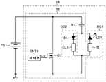
图1是示出第一实施方式的激光装置的概略配置的图。第一实施方式的激光装置1A(下称激光装置1A)包括激光二极管LD1、以及激光二极管驱动电路2A。FIG. 1 is a diagram showing a schematic configuration of a laser device according to the first embodiment. The
激光二极管驱动电路2A包括NMOS(N沟道金属氧化物半导体)晶体管Q1、控制器CNT1、电容器C1、二极管D1、以及电流限制器CL1。在本说明书中,MOS晶体管表示如下的场效应晶体管,该场效应晶体管的栅极被构造为具有至少三个层,即,电导体层或电阻值低的多晶硅等半导体层、绝缘层、以及P型、N型或本征半导体层。即,MOS晶体管的栅极结构不限于由金属、氧化物和半导体组成的三层结构。The laser
虽然在本实施方式例中使用NMOS晶体管Q1作为开关元件,但可以使用除了NMOS晶体管Q1以外的任意开关元件代替NMOS晶体管Q1。虽然在本实施方式中使用二极管D1作为整流元件,但也可以使用除了二极管D1以外的任意整流元件代替二极管D1。Although the NMOS transistor Q1 is used as the switching element in the present embodiment example, any switching element other than the NMOS transistor Q1 may be used instead of the NMOS transistor Q1. Although the diode D1 is used as the rectifying element in this embodiment, any rectifying element other than the diode D1 may be used instead of the diode D1.
电流限制器CLl例如是单个电阻元件。电流限制器CL1可以是例如由多个电阻元件构成而不是单个电阻元件的电阻电路。电流限制器CL1例如可以是单个二极管而不是单个电阻元件。电流限制器CL1例如可以是多个串联连接的二极管而不是单个电阻元件。电流限制器CL1例如可以是在其栅源电压被调整时限制电流的MOS场效应晶体管、在其基极发射极电压被调整时限制电流的双极晶体管等,而不是单个电阻元件。电流限制器CL1不限于元件,而可以是例如电路板上的导线。当导线的一部分用作电流限制器CL1时,可以将对应于电流限制器CL1的导线的部分形成为形状和材料与其他部分不同,使得对应于电流限制器CL1的导线的部分的电阻更高。电流限制器CL1可以是上述示例中的一个以上的组合。例如,电流限制器CL1可以由串联连接的单个电阻元件和单个二极管构成。The current limiter CL1 is, for example, a single resistive element. The current limiter CL1 may be, for example, a resistive circuit composed of a plurality of resistive elements instead of a single resistive element. The current limiter CL1 may be, for example, a single diode instead of a single resistive element. The current limiter CL1 may be, for example, a plurality of diodes connected in series instead of a single resistive element. The current limiter CL1 may be, for example, a MOS field effect transistor that limits current when its gate-source voltage is adjusted, a bipolar transistor that limits current when its base-emitter voltage is adjusted, etc., instead of a single resistive element. The current limiter CL1 is not limited to an element, but may be, for example, a wire on a circuit board. When a part of the wire is used as the current limiter CL1, the part of the wire corresponding to the current limiter CL1 can be formed to be different in shape and material from other parts so that the resistance of the part of the wire corresponding to the current limiter CL1 is higher. The current limiter CL1 may be a combination of one or more of the above examples. For example, the current limiter CL1 may be composed of a single resistive element and a single diode connected in series.
从控制器CNT1输出的栅极信号G1被馈送至NMOS晶体管Q1的栅极。电容器C1的一端和NMOS晶体管Q1的漏极与直流电源PS1的正极连接。电容器C1的另一端与二极管D1的阳极和激光二极管LD1的阴极连接。二极管D1的阴极与电流限制器CL1的一端连接。电流限制器CL1的另一端、激光二极管LD1的阳极、NMOS晶体管Q1的源极以及直流电源PS1的负极与接地电位连接。The gate signal G1 output from the controller CNT1 is fed to the gate of the NMOS transistor Q1. One end of the capacitor C1 and the drain of the NMOS transistor Q1 are connected to the positive electrode of the DC power supply PS1. The other end of the capacitor C1 is connected to the anode of the diode D1 and the cathode of the laser diode LD1. The cathode of the diode D1 is connected to one end of the current limiter CL1. The other end of the current limiter CL1, the anode of the laser diode LD1, the source of the NMOS transistor Q1, and the cathode of the DC power supply PS1 are connected to the ground potential.
包括二极管D1和电流限制器CL1的第二串联电路DC2以使二极管D1的阳极指向阴极的方向与激光二极管LD1的阳极指向阴极的方向相反的方式与包括激光二极管LD1的第一串联电路DC1并联连接。The second series circuit DC2 comprising the diode D1 and the current limiter CL1 is connected in parallel with the first series circuit DC1 comprising the laser diode LD1 in such a way that the direction of the anode of the diode D1 to the cathode is opposite to the direction of the anode of the laser diode LD1 to the cathode .
控制器CNTl利用栅极信号Gl使NMOS晶体管Ql导通和截止。The controller CNT1 turns on and off the NMOS transistor Q1 using the gate signal G1.
当NMOS晶体管Q1截止时,电流从直流电源PS1的正极依次经由电容器C1、二极管D1、电流限制器CL1流向直流电源PS1的负极,因此电容器C1被充电。当直流电源PS1的输出电压变得与电容器C1的电位差大致相等时,电流停止流动,电容器C1的充电停止。When the NMOS transistor Q1 is turned off, current flows from the positive electrode of the DC power supply PS1 to the negative electrode of the DC power supply PS1 via the capacitor C1, the diode D1, and the current limiter CL1 in this order, so the capacitor C1 is charged. When the output voltage of the DC power supply PS1 becomes substantially equal to the potential difference of the capacitor C1, the current stops flowing, and the charging of the capacitor C1 stops.
当NMOS晶体管Q1导通时,由NMOS晶体管Q1、电容器C1、二极管D1、电流限制器CL1以及激光二极管LD1形成闭合电路。闭合电路包括寄生电感。因此,闭合电路是LCR谐振电路。当在电容器C1中存储有电荷的情况下NMOS晶体管Q1由截止转为导通时,LCR谐振电路开始谐振。When the NMOS transistor Q1 is turned on, a closed circuit is formed by the NMOS transistor Q1, the capacitor C1, the diode D1, the current limiter CL1, and the laser diode LD1. A closed circuit includes parasitic inductance. Therefore, the closed circuit is an LCR resonant circuit. When the NMOS transistor Q1 turns from off to on with the charge stored in the capacitor C1, the LCR resonance circuit starts to resonate.
当NMOS晶体中Q1继续导通时,当流过LCR谐振电路的电流I1为正时的电流I1流过的路径包括如图2所示的激光二极管LD1。因此,当正电流I1流过时,激光二极管LD1发光。当电流I1为负时的电流I1流过的路径不包括如图3所示的激光二极管LD1。因此,当负电流I1流过时,激光二极管LD1不发光。这里,在本实施方式中,NMOS晶体管Q1的漏极指向源极的方向被定义为电流I1的正方向,NMOS晶体管Q1的源极指向漏极的方向被定义为电流I1的负方向。When Q1 in the NMOS crystal continues to be turned on, the path through which the current I1 flows when the current I1 flowing through the LCR resonant circuit is positive includes the laser diode LD1 as shown in FIG. 2 . Therefore, when the positive current I1 flows, the laser diode LD1 emits light. The path through which the current I1 flows when the current I1 is negative does not include the laser diode LD1 shown in FIG. 3 . Therefore, when the negative current I1 flows, the laser diode LD1 does not emit light. Here, in this embodiment, the direction in which the drain of the NMOS transistor Q1 points to the source is defined as the positive direction of the current I1, and the direction in which the source of the NMOS transistor Q1 points to the drain is defined as the negative direction of the current I1.
图4是示出本实施方式中的电流I1、参考例中的电流I1以及栅极信号G1的波形的时间图。参考例的激光装置具有从激光装置1A省略电流限制器CL1的配置。在图4中,栅极信号G1的高电平时段,即NMOS晶体管Q1的导通时段被设定为上述LCR谐振电路的谐振时段的一半。FIG. 4 is a timing chart showing the waveforms of the current I1 in the present embodiment, the current I1 in the reference example, and the gate signal G1. The laser device of the reference example has a configuration in which the current limiter CL1 is omitted from the
NMOS晶体管Q1的导通时段表示NMOS晶体管Q1持续导通的时段。具体地,图4中的时间点t1与t2之间的时段是本实施方式中的NMOS晶体管Q1的导通时段。The ON period of the NMOS transistor Q1 represents the period during which the NMOS transistor Q1 is continuously ON. Specifically, the period between the time points t1 and t2 in FIG. 4 is the ON period of the NMOS transistor Q1 in the present embodiment.
在本实施方式中,当NMOS晶体管Q1截止时,此后在图4中的时间点t2与t4之间的时段,负电流I1经由NMOS晶体管Q1的体二极管流动。在图4中的时间点t2与t4之间的时段,电流I1被电流限制器CL1限制。由此抑制电流I1的振荡,因此抑制在时间点t4之后的正电流I1的出现。因此,可以抑制不必要的激光输出。In the present embodiment, when the NMOS transistor Q1 is turned off, a negative current I1 flows through the body diode of the NMOS transistor Q1 during the period between the time points t2 and t4 in FIG. 4 thereafter. During the period between time points t2 and t4 in FIG. 4 , the current I1 is limited by the current limiter CL1 . The oscillation of the current I1 is thereby suppressed, and thus the occurrence of the positive current I1 after the time point t4 is suppressed. Therefore, unnecessary laser output can be suppressed.
电流限制器CL1不包括在正电流I1流过的路径(参见图2)中。因此,电流限制器CL1不会产生激光输出的上升速度低下或激光输出的下降等缺点。The current limiter CL1 is not included in the path through which the positive current I1 flows (see FIG. 2 ). Therefore, the current limiter CL1 does not suffer from disadvantages such as a decrease in the rising speed of the laser output or a drop in the laser output.
相比之下,在参考例中,当NMOS晶体管Q1截止时,此后在图4中的时间点t2与t3之间的时段,负电流I1经由NMOS晶体管Q1的体二极管流动。在参考例中,没有设置电流限制器CL1,因此不抑制电流I1的振荡。因此,在图4的t3至t5之间的时段,正电流I1经由NMOS晶体管Q1的漏源寄生电容流动;在图4的t5至t6之间的时段,负电流I1经由NMOS晶体管Q1的体二极管流动。因此,在图4的时间点t3至t5之间的时段,发生不必要的激光输出。这种不必要的光输出例如可能导致车辆上的激光雷达装置等不正常工作。这里,如果控制器CNT1在图4中的时间点t5以后将NMOS晶体管Q1由导通转为截止,而不是在图4中的时间点t2将NMOS晶体管Q1由导通转为截止,则在图4中的时间点t3至t5之间的时段流动的正电流I1将被限制得更少。这进一步增加正电流I1,并增加不必要的激光输出。In contrast, in the reference example, when the NMOS transistor Q1 is turned off, a negative current I1 flows through the body diode of the NMOS transistor Q1 in the period between the time points t2 and t3 in FIG. 4 thereafter. In the reference example, the current limiter CL1 is not provided, so the oscillation of the current I1 is not suppressed. Therefore, during the period between t3 and t5 in FIG. 4 , the positive current I1 flows through the drain-source parasitic capacitance of the NMOS transistor Q1; during the period between t5 and t6 in FIG. 4 , the negative current I1 flows through the body diode of the NMOS transistor Q1 flow. Therefore, in the period between the time points t3 to t5 of FIG. 4 , unnecessary laser output occurs. Such unnecessary light output may, for example, cause lidar devices on vehicles, etc., to malfunction. Here, if the controller CNT1 turns the NMOS transistor Q1 from on to off after the time point t5 in FIG. 4 , instead of turning the NMOS transistor Q1 from on to off at the time point t2 in FIG. 4 , then in FIG. The positive current I1 flowing in the period between the time points t3 to t5 in 4 will be limited less. This further increases the positive current I1 and increases unnecessary laser output.
从以上讨论可知,激光二极管驱动电路2A和激光装置1A能够抑制不需要的激光输出。As can be seen from the above discussion, the laser
例如,在激光雷达装置中,不必要的激光输出可能会导致错误检测,因此能够抑制不必要的激光输出的激光二极管驱动电路2A和激光装置1A是非常有用的。For example, in a lidar device, unnecessary laser output may cause erroneous detection, so the laser
NMOS晶体管Q1的导通时段越长,导通时段之后的正电流更容易流动。但是,在本实施方式中,由于设置有电流限制器CL1,抑制导通时段之后的正电流;因此可以增加NMOS晶体管Q1的导通时段。即,通过激光二极管驱动电路2A,可以增加NMOS晶体管Q1的导通时段,从而使栅极信号G1的生成和NMOS晶体管Q1的控制容易。The longer the ON period of the NMOS transistor Q1 is, the easier it is for a positive current to flow after the ON period. However, in the present embodiment, since the current limiter CL1 is provided, the positive current after the turn-on period is suppressed; therefore, the turn-on period of the NMOS transistor Q1 can be increased. That is, with the laser
<2.第二实施方式><2. Second Embodiment>
图5是示出第二实施方式的激光装置的概略配置的图。第二实施方式的激光装置1B(下称激光装置1B)包括激光二极管LD1、以及激光二极管驱动电路2B。FIG. 5 is a diagram showing a schematic configuration of a laser device according to a second embodiment. A
激光二极管驱动电路2B具有在激光二极管驱动电路2A中追加分流电阻Rl的配置。在本实施方式中,分流电阻R1包括在第一串联电路DC1中,并且与激光二极管LD1串联连接。The laser
激光二极管驱动电路2B和激光装置1B提供与激光二极管驱动电路2A和激光装置1A相似的效果,并且能够额外地检测流过激光二极管LD1的电流。The laser
分流电阻Rl检测流过激光二极管LDl的电流。The shunt resistor R1 detects the current flowing through the laser diode LD1.
分流电阻Rl的高电阻值使电流Il的最大值减小,并且减缓激光输出的上升。因此,为分流电阻R1给定低电阻值很重要。相应地,在本实施方式中,分流电阻R1的阻抗被设定为低于电流限制器CL1的阻抗。The high resistance value of the shunt resistor R1 reduces the maximum value of the current I1 and slows down the rise of the laser output. Therefore, it is important to give the shunt resistor R1 a low resistance value. Accordingly, in the present embodiment, the impedance of the shunt resistor R1 is set to be lower than the impedance of the current limiter CL1.
<3.第三实施方式><3. Third Embodiment>
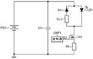
图6是示出第三实施方式的激光装置的概略配置的图。第三实施方式的激光装置1C(下称激光装置1C)包括激光二极管LD1、以及激光二极管驱动电路2C。FIG. 6 is a diagram showing a schematic configuration of a laser device according to a third embodiment. A
激光二极管驱动电路2C具有在激光二极管驱动电路2A中追加分流电阻Rl的配置。在本实施方式中,分流电阻R1与由第一串联电路DC1和第二串联电路DC2连接在一起形成的并联电路串联连接。The laser
激光二极管驱动电路2C和激光装置1C提供与激光二极管驱动电路2A和激光装置1A相似的效果,并且能够额外地检测流过激光二极管LDl的电流。The laser
分流电阻R1检测流过激光二极管LD1的电流。这里,在本实施方式中,不同于第二实施方式,分流电阻R1以包括二极管D1的恢复电流的方式检测流过激光二极管LD1的电流。因此,在第二实施方式中检测流过激光二极管LD1的电流的精度高于本实施方式。The shunt resistor R1 detects the current flowing through the laser diode LD1. Here, in the present embodiment, unlike the second embodiment, the shunt resistor R1 detects the current flowing through the laser diode LD1 so as to include the recovery current of the diode D1. Therefore, the accuracy of detecting the current flowing through the laser diode LD1 is higher in the second embodiment than in the present embodiment.
分流电阻Rl的高电阻值使电流Il的最大值减小,并且减缓激光输出的上升。因此,为分流电阻R1给定低电阻值很重要。相应地,在本实施方式中,分流电阻R1的阻抗被设定为低于电流限制器CL1的阻抗。The high resistance value of the shunt resistor R1 reduces the maximum value of the current I1 and slows down the rise of the laser output. Therefore, it is important to give the shunt resistor R1 a low resistance value. Accordingly, in the present embodiment, the impedance of the shunt resistor R1 is set to be lower than the impedance of the current limiter CL1.
<4.分流电阻><4. Shunt resistance>
图7是示出在第二、第三实施方式中使用的分流电阻R1的配置例的图。图7所示的配置例中的分流电阻R1具有并联连接的多个电阻元件RE1。通过将多个电阻元件RE1并联连接,容易减小分流电阻R1的电阻值。FIG. 7 is a diagram showing an example of the arrangement of the shunt resistors R1 used in the second and third embodiments. The shunt resistor R1 in the arrangement example shown in FIG. 7 has a plurality of resistance elements RE1 connected in parallel. By connecting the plurality of resistance elements RE1 in parallel, the resistance value of the shunt resistance R1 can be easily reduced.
虽然在图7所示的配置例中并联连接有3个电阻元件RE1,但并联连接的电阻元件的个数不限于3个,可以是大于1的任意个数。并联连接的电阻元件RE1的个数越多,越容易减小分流电阻R1的电阻值,但分流电阻R1的安装面积越大。因此,可以考虑所要求的分流电阻R1的电阻值和所要求的分流电阻R1的安装面积之间的折衷来决定并联连接的电阻元件RE1的个数。Although three resistance elements RE1 are connected in parallel in the arrangement example shown in FIG. 7 , the number of resistance elements connected in parallel is not limited to three, and may be any number greater than one. The greater the number of resistance elements RE1 connected in parallel, the easier it is to reduce the resistance value of the shunt resistor R1, but the larger the mounting area of the shunt resistor R1. Therefore, the number of resistance elements RE1 connected in parallel can be determined in consideration of a trade-off between the required resistance value of the shunt resistor R1 and the required mounting area of the shunt resistor R1.
为了防止LCR谐振电路的谐振周期冗长的同时使电流I1的最大值增大,优选LCR谐振电路的电感分量较小。为了使在图7所示的配置例的分流电阻R1中形成的寄生电感最小化,优选相邻电阻元件RE1之间的互感M为零。In order to prevent the resonant period of the LCR resonant circuit from being redundant and to increase the maximum value of the current I1, it is preferable that the inductance component of the LCR resonant circuit is small. In order to minimize the parasitic inductance formed in the shunt resistance R1 of the arrangement example shown in FIG. 7 , it is preferable that the mutual inductance M between the adjacent resistance elements RE1 be zero.
相邻电阻元件RE1的互感M可以由以下公式(1)给出。这里,LN表示电阻元件RE1的长度,d表示相邻电阻元件RE1之间的间隔。互感M的单位是亨利(H),长度LN和间隔d的单位均为米(m)。The mutual inductance M of the adjacent resistance elements RE1 can be given by the following formula (1). Here, LN represents the length of the resistance element RE1, and d represents the interval between adjacent resistance elements RE1. The unit of mutual inductance M is Henry (H), and the unit of length LN and interval d are both meters (m).
M=2LN(1n(2LN/d)-1)×10-7 (1)M=2LN(1n(2LN/d)-1)×10-7 (1)
因此,用于使互感M保持为零的条件可以由下面的公式(2)给出。这里,e表示纳皮尔常数。Therefore, the condition for keeping the mutual inductance M at zero can be given by the following formula (2). Here, e represents Napier's constant.
In(2LN/d)-1≤0In(2LN/d)-1≤0
d≥2LN/e (2)d≥2LN/e (2)
即,优选相邻电阻元件RE1之间的间隔d为电阻元件RE1的长度LN的两倍除以纳皮尔常数所得的值以上。That is, the interval d between adjacent resistance elements RE1 is preferably equal to or greater than a value obtained by dividing twice the length LN of the resistance elements RE1 by the Napier constant.
<5.开关元件><5. Switching element>
优选地,当设置在每个激光二极管驱动电路2A至2C中的NMOS晶体管Q1截止时,NMOS晶体管Q1的体二极管两端的正向电压高于一般的硅二极管两端的正向电压(例如,0.7V)。如果NMOS晶体管Q1的体二极管两端的正向电压在其截止时为高,则电流I1的振荡不仅被电流限制器CL1抑制,而且还被体二极管抑制;因此,可以进一步抑制不必要的激光输出。如果电流I1的振荡被电流限制器CL1充分抑制,则在NMOS晶体管Q1截止时,NMOS晶体管Q1的体二极管两端的正向电压无需高于一般的硅二极管两端的正向电压(例如,0.7V)。在NMOS晶体管Q1截止时,如果NMOS晶体管Q1的体二极管两端的正向电压不高于一般的硅二极管两端的正向电压(例如,0.7V),则可以将“反接二极管”与NMOS晶体管Q1并联连接。“反接二极管”的阳极与NMOS晶体管Q1的源极连接,“反接二极管”的阴极与NMOS晶体管Q1的漏极连接。“反接二极管”的整流方向与二极管D1相同。作为“反接二极管”,例如,可以使用正向电压约为0.3V的二极管。正向电压约为0.3V的二极管的一例是SBD(Schottky BarrierDiode,肖特基势垒二极管)。因此,作为“反接二极管”,例如,可以使用SBD(SchottkyBarrier Diode,肖特基势垒二极管)。Preferably, when the NMOS transistor Q1 provided in each of the laser
当NMOS晶体管Q1例如是使用硅半导体的开关元件时,通过将NMOS晶体管Q1截止时的NMOS晶体管Q1的栅源电压设定为负值,即通过将NMOS晶体管截止时的栅极信号G1的电平设定得低于接地电位,可以将NMOS晶体管Q1的体二极管两端的正向电压设定得高于一般的硅二极管两端的正向电压(例如,0.7V)。When the NMOS transistor Q1 is, for example, a switching element using a silicon semiconductor, the gate-source voltage of the NMOS transistor Q1 when the NMOS transistor Q1 is turned off is set to a negative value, that is, by setting the level of the gate signal G1 when the NMOS transistor is turned off Set lower than ground potential, the forward voltage across the body diode of NMOS transistor Q1 can be set higher than the forward voltage across a typical silicon diode (eg, 0.7V).
通过将NMOS晶体管Q1截止时的NMOS晶体管Q1的栅源电压设定为负值,可以防止NMOS晶体管Q1在NMOS晶体管Q1理应截止的时段错误地导通。通过防止NMOS晶体管Q1错误地导通,可以进一步抑制不必要的激光输出。By setting the gate-source voltage of the NMOS transistor Q1 to a negative value when the NMOS transistor Q1 is turned off, the NMOS transistor Q1 can be prevented from being erroneously turned on during a period when the NMOS transistor Q1 should be turned off. By preventing the NMOS transistor Q1 from being erroneously turned on, unnecessary laser output can be further suppressed.
例如,也可以通过将使用带隙大于硅半导体的宽带隙半导体的开关元件用作NMOS晶体管Ql,将NMOS晶体管Q1的体二极管两端的正向电压设定得高于一般的硅二极管两端的正向电压(例如,0.7V)。带隙大于硅半导体的宽带隙半导体例如可以是SiC、GaN等化合物半导体。For example, the forward voltage across the body diode of the NMOS transistor Q1 may be set higher than the forward voltage across a general silicon diode by using a switching element using a wide-bandgap semiconductor with a larger band gap than a silicon semiconductor as the NMOS transistor Q1. voltage (eg, 0.7V). The wide band gap semiconductor with a band gap larger than that of the silicon semiconductor may be, for example, compound semiconductors such as SiC and GaN.
通过选择输出电容Coss较小的晶体管作为NMOS晶体管Ql,抑制电流Il的振荡;因此,可以进一步抑制不必要的激光输出。输出容量Coss较小的晶体管例如可以是由带隙大于硅半导体的宽带隙半导体形成的晶体管。By selecting a transistor with a smaller output capacitance Coss as the NMOS transistor Q1, oscillation of the current I1 is suppressed; therefore, unnecessary laser output can be further suppressed. The transistor whose output capacity Coss is small may be, for example, a transistor formed of a wide-bandgap semiconductor whose band gap is larger than that of a silicon semiconductor.
通过选择输入电容Ciss较小的晶体管作为NMOS晶体管Q1,提高NMOS晶体管Q1导通时段的控制性能;这使得更容易抑制不必要的激光输出。输入电容Ciss较小的晶体管例如可以是由带隙大于硅半导体的宽带隙半导体形成的晶体管。By selecting a transistor with a smaller input capacitance Ciss as the NMOS transistor Q1, the control performance of the ON period of the NMOS transistor Q1 is improved; this makes it easier to suppress unnecessary laser output. The transistor with a smaller input capacitance Ciss may be, for example, a transistor formed of a wide-bandgap semiconductor with a larger bandgap than a silicon semiconductor.
<6.构件布局><6. Component layout>
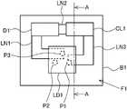
图8至图10是示出第一实施方式的构件布局的一例的图。图8是安装有NMOS晶体管Q1、电容器C1、二极管D1、电流限制器CL1以及激光二极管LD1的电路板B1的顶视图。图9是安装有NMOS晶体管Q1、电容器C1、二极管D1、电流限制器CL1以及激光二极管LD1的电路板B1的底视图。图10是沿图8和图9中的剖面AA剖切的安装有NMOS晶体管Q1、电容器C1、二极管D1、电流限制器CL1以及激光二极管LD1的电路板B1的剖视图。图10中的虚线表示电路板B1的第一面F1和第二面F2的法线方向。电路板B1的第一面F1和第二面F2彼此背向且实质上平行。这里,术语“顶视图”和“底视图”是为了方便起见而使用的,并不意味着限制激光装置的设置方式。8 to 10 are diagrams showing an example of the component layout of the first embodiment. FIG. 8 is a top view of the circuit board B1 on which the NMOS transistor Q1 , the capacitor C1 , the diode D1 , the current limiter CL1 , and the laser diode LD1 are mounted. FIG. 9 is a bottom view of the circuit board B1 on which the NMOS transistor Q1 , the capacitor C1 , the diode D1 , the current limiter CL1 , and the laser diode LD1 are mounted. 10 is a cross-sectional view of the circuit board B1 on which the NMOS transistor Q1 , the capacitor C1 , the diode D1 , the current limiter CL1 , and the laser diode LD1 are mounted, taken along the section AA in FIGS. 8 and 9 . The dotted line in FIG. 10 indicates the normal direction of the first surface F1 and the second surface F2 of the circuit board B1. The first surface F1 and the second surface F2 of the circuit board B1 face away from each other and are substantially parallel. Here, the terms "top view" and "bottom view" are used for convenience and are not meant to limit how the laser device is arranged.
如图8所示,在电路基板B1的第一面F1上设置有导线LN1至LN3。导线LN1是将TO-Can封装激光二极管LD1的3号引脚(激光二极管的阴极)P3与二极管D1的阳极电连接的导线。导线LN2是将二极管D1的阴极与电流限制器CL1的一端电连接的导线。导线LN3是将电流限制器CL1的另一端与TO-Can封装激光二极管LD1的1号引脚(激光二极管的阳极)P1电连接的导线。As shown in FIG. 8, lead wires LN1 to LN3 are provided on the first surface F1 of the circuit board B1. The lead LN1 is a lead for electrically connecting the third pin (the cathode of the laser diode) P3 of the TO-Can package laser diode LD1 and the anode of the diode D1. The lead LN2 is a lead that electrically connects the cathode of the diode D1 and one end of the current limiter CL1. The lead LN3 is a lead for electrically connecting the other end of the current limiter CL1 to the pin No. 1 (anode of the laser diode) P1 of the TO-Can package laser diode LD1.
TO-Can封装激光二极管LD1的2号引脚P2是内置于To-Can封装中的光接收元件的阴极。Pin No. 2 P2 of the TO-Can package laser diode LD1 is the cathode of the light receiving element built into the To-Can package.
电路板B1形成有TO-Can封装激光二极管LD1的1号引脚P1至3号引脚P3分别贯通的通孔。每个通孔在电路板B1的第一面F1和第二面F2的法线方向上延伸。The circuit board B1 is formed with through-holes through which the first pin P1 to the third pin P3 of the TO-Can package laser diode LD1 pass through, respectively. Each of the through holes extends in the normal direction of the first and second faces F1 and F2 of the circuit board B1.
如图9所示,在电路板B1的第二面F2上,设置有导线LN4至LN6。导线LN4将TO-Can封装激光二极管LD1的3号引脚(激光二极管的阴极)P3与电容器C1的一个端子电连接。导线LN5将TO-Can封装激光二极管LD1的1号引脚(激光二极管的阳极)P1与NMOS晶体管Q1的源极电连接。导线LN6将NMOS晶体管Q1的漏极与电容器C1的另一端电连接。As shown in FIG. 9, on the second surface F2 of the circuit board B1, wires LN4 to LN6 are provided. The lead LN4 electrically connects the pin No. 3 (the cathode of the laser diode) P3 of the TO-Can package laser diode LD1 to one terminal of the capacitor C1. A lead LN5 electrically connects pin 1 (the anode of the laser diode) P1 of the TO-Can packaged laser diode LD1 to the source of the NMOS transistor Q1. Conductor LN6 electrically connects the drain of NMOS transistor Q1 to the other end of capacitor C1.
在图8至图10所示的第一实施方式中的构件布局的示例中,激光二极管LD1安装在电路板B1的第一面F1上,NMOS晶体管Q1和电容器C1安装在电路板B1的第二面F2上。这样,可以缩短正电流I1流过的路径(参见图2至图10中的粗箭头)。这有助于减小正电流I1流过的路径中的导线电感。因此,可以防止LCR谐振电路的谐振周期冗长的同时使电流I1的最大值增大。In the example of the component layout in the first embodiment shown in FIGS. 8 to 10 , the laser diode LD1 is mounted on the first side F1 of the circuit board B1 , and the NMOS transistor Q1 and the capacitor C1 are mounted on the second side of the circuit board B1 face F2. In this way, the path through which the positive current I1 flows can be shortened (see the thick arrows in FIGS. 2 to 10 ). This helps reduce the wire inductance in the path through which the positive current I1 flows. Therefore, the maximum value of the current I1 can be increased while preventing the resonant period of the LCR resonance circuit from being redundant.
这里,优选地,从电路板B1的第一面F1和第二面F2的法线方向看,NMOS晶体管Q1和电容器C1中的至少一个的至少一部分与激光二极管LD1重叠。这样,更容易缩短正电流I1流过的路径。Here, preferably, at least a part of at least one of the NMOS transistor Q1 and the capacitor C1 overlaps the laser diode LD1 as viewed from the normal direction of the first and second surfaces F1 and F2 of the circuit board B1. In this way, it is easier to shorten the path through which the positive current I1 flows.
虽然以上描述论及第一实施方式中的构件布局的一例,但在第二、第三实施方式中也采用类似的构件布局有助于减小正电流I1流过的路径中的导线电感。这里,分流电阻R1可以设置在第一面F1和第二面F2中的任一个上。Although the above description refers to an example of the component layout in the first embodiment, the use of similar component layouts in the second and third embodiments helps to reduce the wire inductance in the path through which the positive current I1 flows. Here, the shunt resistor R1 may be provided on any one of the first face F1 and the second face F2.
<7.用途><7. Purpose>
作为可以是上述激光装置1A~1C中的任一个的激光装置1例如被用作图11所示的激光雷达装置X1的一部分。图11所示的激光雷达装置X1是一种扫描激光雷达装置,并且包括激光装置1、光接收器3、光学系统4、以及整体控制器5。整体控制器5控制激光装置1的输出和光学系统4中的反射镜的方向,基于激光装置1的输出的控制方式和光接收器3的输出信号来计算到物体的距离,并基于光学系统4中的反射镜的方向的控制方式来计算物体的方向。The
图11所示的激光雷达装置X1例如设置在如图12所示的车辆Y1的前端,并且感测位于车辆Y1前方的物体。The lidar device X1 shown in FIG. 11 is provided, for example, at the front end of the vehicle Y1 shown in FIG. 12 , and senses an object located in front of the vehicle Y1 .
<8.其他变更><8. Other changes>
本说明书中公开的实施方式在各个方面都应被视为是说明示例性的,而不是限制性的,本发明的技术范围不由以上给出的实施方式的描述定义,而是由所附权利要求书的范围定义,并且应被理解为含括落入与权利要求书等效的意义和范围内的变更。The embodiments disclosed in this specification should be regarded as illustrative and non-restrictive in all aspects, and the technical scope of the present invention is defined not by the description of the embodiments given above, but by the appended claims The scope of the book is defined, and should be construed to include changes that come within the meaning and range equivalent to the claims.
例如,电容器C1、由第一串联电路DC1和第二串联电路DC2形成的并联电路以及NMOS晶体管Q1的连接顺序无需在如图1至图5所示的配置中那样。原因在于,由于电容器C1、由第一串联电路DC1和第二串联电路DC2形成的并联电路以及NMOS晶体管Q1串联连接,因而即使以不同的顺序连接,也能够获得相似的效果。但是,如果NMOS晶体管Q1的体二极管相对于二极管D1和激光二极管LD1的方向变得与连接顺序的变更前的方向相反,则有必要使二极管D1和激光二极管LD1的方向也相反。相应地,例如,在图13所示的配置中,与图1所示的配置相比,不仅电容器C1、由第一串联电路DC1和第二串联电路DC2形成的并联电路以及NMOS晶体管Q1的连接顺序发生变化,而且二极管D1和激光二极管LD1的方向也发生了变化。又例如,电容器C1、由第一串联电路DC1和第二串联电路DC2形成的并联电路、分流电阻R1以及NMOS晶体管Q1的连接顺序无需在如图6所示的配置中那样。原因在于,由于电容器C1、由第一串联电路DC1和第二串联电路DC2形成的并联电路、分流电阻R1以及NMOS晶体管Q1串联连接,因而即使以不同的顺序连接,也能够获得相似的效果。但是,如果NMOS晶体管Q1的体二极管相对于二极管D1和激光二极管LD1的方向变得与连接顺序的变更之前的方向相反,则有必要使二极管D1和激光二极管LD1的方向也相反。相应地,例如,在图14所示的配置中,与图6所示的配置相比,不仅电容器C1、由第一串联电路DC1和第二串联电路DC2形成的并联电路、分流电阻R1以及NMOS晶体管Q1的连接顺序发生变化,而且二极管D1和激光二极管LD1的方向也发生的变化。这里,在激光二极管驱动电路包括分流电阻R1的配置中,优选地,分流电阻R1的一端与接地电位连接,从而以接地电位为基准给出电流感测结果。For example, the connection order of the capacitor C1 , the parallel circuit formed by the first series circuit DC1 and the second series circuit DC2 , and the NMOS transistor Q1 need not be as in the configurations shown in FIGS. 1 to 5 . The reason is that since the capacitor C1, the parallel circuit formed by the first series circuit DC1 and the second series circuit DC2, and the NMOS transistor Q1 are connected in series, similar effects can be obtained even if connected in a different order. However, if the direction of the body diode of the NMOS transistor Q1 with respect to the diode D1 and the laser diode LD1 is reversed from the direction before the connection order is changed, the direction of the diode D1 and the laser diode LD1 must also be reversed. Accordingly, for example, in the configuration shown in FIG. 13 , compared with the configuration shown in FIG. 1 , not only the capacitor C1 , the parallel circuit formed by the first series circuit DC1 and the second series circuit DC2 , and the connection of the NMOS transistor Q1 The sequence is changed, and the direction of diode D1 and laser diode LD1 is also changed. For another example, the connection order of the capacitor C1 , the parallel circuit formed by the first series circuit DC1 and the second series circuit DC2 , the shunt resistor R1 and the NMOS transistor Q1 need not be as in the configuration shown in FIG. 6 . The reason is that since the capacitor C1, the parallel circuit formed by the first series circuit DC1 and the second series circuit DC2, the shunt resistor R1, and the NMOS transistor Q1 are connected in series, similar effects can be obtained even if connected in a different order. However, if the direction of the body diode of the NMOS transistor Q1 with respect to the diode D1 and the laser diode LD1 is reversed from that before the connection order is changed, the direction of the diode D1 and the laser diode LD1 must also be reversed. Accordingly, for example, in the configuration shown in FIG. 14 , compared with the configuration shown in FIG. 6 , not only the capacitor C1 , the parallel circuit formed by the first series circuit DC1 and the second series circuit DC2 , the shunt resistance R1 , and the NMOS The connection order of the transistor Q1 is changed, and the direction of the diode D1 and the laser diode LD1 is also changed. Here, in the configuration in which the laser diode drive circuit includes the shunt resistor R1, preferably, one end of the shunt resistor R1 is connected to the ground potential, so that the current sensing result is given with reference to the ground potential.
激光装置不限于安装在电路板上的一种类型。例如,可以将激光二极管驱动电路的至少一部分与激光二极管一起内置到模块中并容纳在Can封装的内部,或者可以将激光装置的至少一部分内置到模块中并容纳在除了Can封装以外的容器的内部。The laser device is not limited to one type mounted on a circuit board. For example, at least a portion of the laser diode driver circuit may be built into the module together with the laser diode and housed inside the Can package, or at least a portion of the laser device may be built into the module and housed inside a container other than the Can package .
例如,本说明书中公开的不同实施方式和变形例可以以任意可行的组合来实施。For example, the various embodiments and modifications disclosed in this specification can be implemented in any feasible combination.
附图标记说明Description of reference numerals
1A 第一实施方式的激光装置1A Laser device of first embodiment
1B 第二实施方式的激光装置1B Laser device of the second embodiment
1C 第三实施方式的激光装置1C Laser device of the third embodiment
2A、2B、2C 激光二极管驱动电路2A, 2B, 2C Laser Diode Driver Circuit
B1 电路板B1 circuit board
C1 电容器C1 capacitor
CL1 电流限制器CL1 Current Limiter
CNT1 控制器CNT1 controller
D1 二极管D1 diode
DC1 第一串联电路DC1 first series circuit
DC2 第二串联电路DC2 second series circuit
LD1 激光二极管LD1 Laser Diode
R1 分流电阻R1 Shunt Resistor
RE1 电阻元件RE1 Resistive element
Q1 NMOS晶体管Q1 NMOS transistor
X1 激光雷达装置X1 lidar unit
Y1 车辆Y1 vehicle
Claims (13)
Applications Claiming Priority (3)
| Application Number | Priority Date | Filing Date | Title |
|---|---|---|---|
| JP2019192903 | 2019-10-23 | ||
| JP2019-192903 | 2019-10-23 | ||
| PCT/JP2020/032145WO2021079611A1 (en) | 2019-10-23 | 2020-08-26 | Laser diode drive circuit |
Publications (1)
| Publication Number | Publication Date |
|---|---|
| CN114616732Atrue CN114616732A (en) | 2022-06-10 |
Family
ID=75620466
Family Applications (1)
| Application Number | Title | Priority Date | Filing Date |
|---|---|---|---|
| CN202080074065.4APendingCN114616732A (en) | 2019-10-23 | 2020-08-26 | Laser diode driving circuit |
Country Status (5)
| Country | Link |
|---|---|
| US (1) | US12424820B2 (en) |
| JP (1) | JP7611157B2 (en) |
| CN (1) | CN114616732A (en) |
| DE (1) | DE112020005138T5 (en) |
| WO (1) | WO2021079611A1 (en) |
Families Citing this family (3)
| Publication number | Priority date | Publication date | Assignee | Title |
|---|---|---|---|---|
| US11955770B2 (en)* | 2020-12-28 | 2024-04-09 | Lumentum Operations Llc | Laser diode assembly and driving circuit for high power short pulse generation |
| EP4413640A1 (en) | 2021-10-07 | 2024-08-14 | Signify Holding B.V. | Active current shifting for lasers to rebalance lasing current differences |
| JP2023181772A (en)* | 2022-06-13 | 2023-12-25 | 株式会社デンソー | Light emitting unit and optical sensor |
Citations (4)
| Publication number | Priority date | Publication date | Assignee | Title |
|---|---|---|---|---|
| CN101490503A (en)* | 2006-07-17 | 2009-07-22 | 莱卡地球系统公开股份有限公司 | Electro-optical range finder |
| US20150372451A1 (en)* | 2013-02-28 | 2015-12-24 | Lawrence Livermore National Security, Llc | Compact high current, high efficiency laser diode driver |
| JP2018077073A (en)* | 2016-11-08 | 2018-05-17 | オムロンオートモーティブエレクトロニクス株式会社 | Object detection device |
| US20180261975A1 (en)* | 2017-03-07 | 2018-09-13 | Sensl Technologies Ltd. | Laser driver |
Family Cites Families (14)
| Publication number | Priority date | Publication date | Assignee | Title |
|---|---|---|---|---|
| JPH10502181A (en) | 1994-06-20 | 1998-02-24 | ネオマジック・コーポレイション | Graphics controller integrated circuit without memory interface |
| JP2002208677A (en) | 2001-01-12 | 2002-07-26 | Toyota Industries Corp | Semiconductor device with temperature detection function |
| JP2002333476A (en) | 2001-05-09 | 2002-11-22 | Denso Corp | Light-emitting circuit for instrument for measuring distance |
| US6798797B2 (en)* | 2001-06-07 | 2004-09-28 | Science Research Laboratory, Inc. | Method and apparatus for driving laser diode sources |
| JP2003149338A (en)* | 2001-11-09 | 2003-05-21 | Denso Corp | Object recognition device and distance measuring device |
| US7935616B2 (en)* | 2004-06-17 | 2011-05-03 | Burgener Ii Robert H | Dynamic p-n junction growth |
| FR3004592B1 (en)* | 2013-04-10 | 2016-08-05 | Brightloop | BODY FOR CONTROLLING AT LEAST ONE LASER DIODE |
| JP6097713B2 (en)* | 2014-03-19 | 2017-03-15 | 古河電気工業株式会社 | Light emitting element driving circuit, light source device, and light emitting element driving method |
| US9054485B1 (en)* | 2014-09-17 | 2015-06-09 | Hong Kong Applied Science & Technology Research Institute Company, Ltd. | Asymmetric edge compensation of both anode and cathode terminals of a vertical-cavity surface-emitting laser (VCSEL) diode |
| US10097908B2 (en)* | 2014-12-31 | 2018-10-09 | Macom Technology Solutions Holdings, Inc. | DC-coupled laser driver with AC-coupled termination element |
| JP6569236B2 (en) | 2015-02-18 | 2019-09-04 | 株式会社豊田中央研究所 | Laser diode drive circuit and laser radar device |
| US10256605B2 (en) | 2016-10-14 | 2019-04-09 | Waymo Llc | GaNFET as energy store for fast laser pulser |
| US10454472B2 (en) | 2016-12-01 | 2019-10-22 | Efficient Power Conversion Corporation | Bootstrap capacitor over-voltage management circuit for GaN transistor based power converters |
| DE102017219413B4 (en) | 2017-10-30 | 2021-11-04 | Robert Bosch Gmbh | Method for generating a laser pulse |
- 2020
- 2020-08-26WOPCT/JP2020/032145patent/WO2021079611A1/ennot_activeCeased
- 2020-08-26JPJP2021554111Apatent/JP7611157B2/enactiveActive
- 2020-08-26USUS17/767,245patent/US12424820B2/enactiveActive
- 2020-08-26DEDE112020005138.2Tpatent/DE112020005138T5/enactivePending
- 2020-08-26CNCN202080074065.4Apatent/CN114616732A/enactivePending
Patent Citations (4)
| Publication number | Priority date | Publication date | Assignee | Title |
|---|---|---|---|---|
| CN101490503A (en)* | 2006-07-17 | 2009-07-22 | 莱卡地球系统公开股份有限公司 | Electro-optical range finder |
| US20150372451A1 (en)* | 2013-02-28 | 2015-12-24 | Lawrence Livermore National Security, Llc | Compact high current, high efficiency laser diode driver |
| JP2018077073A (en)* | 2016-11-08 | 2018-05-17 | オムロンオートモーティブエレクトロニクス株式会社 | Object detection device |
| US20180261975A1 (en)* | 2017-03-07 | 2018-09-13 | Sensl Technologies Ltd. | Laser driver |
Also Published As
| Publication number | Publication date |
|---|---|
| JPWO2021079611A1 (en) | 2021-04-29 |
| WO2021079611A1 (en) | 2021-04-29 |
| JP7611157B2 (en) | 2025-01-09 |
| US12424820B2 (en) | 2025-09-23 |
| US20220376470A1 (en) | 2022-11-24 |
| DE112020005138T5 (en) | 2022-07-21 |
Similar Documents
| Publication | Publication Date | Title |
|---|---|---|
| US20230317713A1 (en) | Semiconductor Device | |
| US9960153B2 (en) | Semiconductor device and electronic apparatus of a cascode-coupled system | |
| CN114616732A (en) | Laser diode driving circuit | |
| JP5858914B2 (en) | Power module and output circuit | |
| US9762053B2 (en) | Load driving device | |
| CN112840566B (en) | Electronic circuit and sensor system | |
| US20180248540A1 (en) | Switching circuit | |
| US20220285911A1 (en) | Semiconductor laser device | |
| US20170279446A1 (en) | Semiconductor device | |
| CN113875140B (en) | Driver circuit and switching system | |
| US11418182B2 (en) | Switch circuitry | |
| KR20220046650A (en) | switching module | |
| US20060027220A1 (en) | Engine ignition system having noise protection circuit | |
| JP2020136288A (en) | Semiconductor device | |
| US20150062764A1 (en) | Esd protection circuit | |
| JP7245663B2 (en) | semiconductor equipment | |
| US20240405765A1 (en) | Gate drive circuit, electric power conversion device | |
| CN113689814A (en) | Driving circuit | |
| JP4770119B2 (en) | MOS type semiconductor device and ignition device provided with the same | |
| US20240355717A1 (en) | Integrated bidirectional four quadrant switches with drivers and input/output circuits | |
| JP6013059B2 (en) | Switch control circuit, igniter, engine ignition device, vehicle | |
| JP2018152781A (en) | Surge suppression circuit | |
| WO2024157648A1 (en) | Semiconductor device, inverter, dc/dc converter, switching power supply device, motor drive circuit, and vehicle | |
| WO2015060095A1 (en) | Sensor device | |
| WO2024024138A1 (en) | Short-circuit protection circuit, semiconductor device, and short-circuit protection method |
Legal Events
| Date | Code | Title | Description |
|---|---|---|---|
| PB01 | Publication | ||
| PB01 | Publication | ||
| SE01 | Entry into force of request for substantive examination | ||
| SE01 | Entry into force of request for substantive examination |