CN114613899A - Display panel and display device - Google Patents
Display panel and display deviceDownload PDFInfo
- Publication number
- CN114613899A CN114613899ACN202210230493.2ACN202210230493ACN114613899ACN 114613899 ACN114613899 ACN 114613899ACN 202210230493 ACN202210230493 ACN 202210230493ACN 114613899 ACN114613899 ACN 114613899A
- Authority
- CN
- China
- Prior art keywords
- electrode
- substrate
- unit
- eutectic
- display panel
- Prior art date
- Legal status (The legal status is an assumption and is not a legal conclusion. Google has not performed a legal analysis and makes no representation as to the accuracy of the status listed.)
- Pending
Links
Images


Classifications
- H—ELECTRICITY
- H10—SEMICONDUCTOR DEVICES; ELECTRIC SOLID-STATE DEVICES NOT OTHERWISE PROVIDED FOR
- H10H—INORGANIC LIGHT-EMITTING SEMICONDUCTOR DEVICES HAVING POTENTIAL BARRIERS
- H10H20/00—Individual inorganic light-emitting semiconductor devices having potential barriers, e.g. light-emitting diodes [LED]
- H10H20/80—Constructional details
- H10H20/85—Packages
- H10H20/857—Interconnections, e.g. lead-frames, bond wires or solder balls
- H—ELECTRICITY
- H01—ELECTRIC ELEMENTS
- H01L—SEMICONDUCTOR DEVICES NOT COVERED BY CLASS H10
- H01L25/00—Assemblies consisting of a plurality of semiconductor or other solid state devices
- H01L25/16—Assemblies consisting of a plurality of semiconductor or other solid state devices the devices being of types provided for in two or more different subclasses of H10B, H10D, H10F, H10H, H10K or H10N, e.g. forming hybrid circuits
- H01L25/167—Assemblies consisting of a plurality of semiconductor or other solid state devices the devices being of types provided for in two or more different subclasses of H10B, H10D, H10F, H10H, H10K or H10N, e.g. forming hybrid circuits comprising optoelectronic devices, e.g. LED, photodiodes
- H—ELECTRICITY
- H10—SEMICONDUCTOR DEVICES; ELECTRIC SOLID-STATE DEVICES NOT OTHERWISE PROVIDED FOR
- H10D—INORGANIC ELECTRIC SEMICONDUCTOR DEVICES
- H10D86/00—Integrated devices formed in or on insulating or conducting substrates, e.g. formed in silicon-on-insulator [SOI] substrates or on stainless steel or glass substrates
- H10D86/40—Integrated devices formed in or on insulating or conducting substrates, e.g. formed in silicon-on-insulator [SOI] substrates or on stainless steel or glass substrates characterised by multiple TFTs
- H10D86/441—Interconnections, e.g. scanning lines
- H—ELECTRICITY
- H10—SEMICONDUCTOR DEVICES; ELECTRIC SOLID-STATE DEVICES NOT OTHERWISE PROVIDED FOR
- H10D—INORGANIC ELECTRIC SEMICONDUCTOR DEVICES
- H10D86/00—Integrated devices formed in or on insulating or conducting substrates, e.g. formed in silicon-on-insulator [SOI] substrates or on stainless steel or glass substrates
- H10D86/40—Integrated devices formed in or on insulating or conducting substrates, e.g. formed in silicon-on-insulator [SOI] substrates or on stainless steel or glass substrates characterised by multiple TFTs
- H10D86/60—Integrated devices formed in or on insulating or conducting substrates, e.g. formed in silicon-on-insulator [SOI] substrates or on stainless steel or glass substrates characterised by multiple TFTs wherein the TFTs are in active matrices
Landscapes
- Engineering & Computer Science (AREA)
- Microelectronics & Electronic Packaging (AREA)
- Physics & Mathematics (AREA)
- Condensed Matter Physics & Semiconductors (AREA)
- General Physics & Mathematics (AREA)
- Computer Hardware Design (AREA)
- Power Engineering (AREA)
- Electroluminescent Light Sources (AREA)
Abstract
Description
Translated fromChinese技术领域technical field
本申请涉及显示领域,尤其涉及一种显示面板以及一种包括该显示面板的显示装置。The present application relates to the field of display, and in particular, to a display panel and a display device including the display panel.
背景技术Background technique
随着显示技术的发展,显示面板的应用越来越普遍,已经逐渐成为人们日常工作和生活所必不可少的组成部分。因此,显示面板的研究成为本领域技术人员的研究热点。With the development of display technology, the application of display panels has become more and more common, and has gradually become an indispensable part of people's daily work and life. Therefore, research on display panels has become a research hotspot for those skilled in the art.
在发光二极管(Light Emitting Diode,LED)显示面板中,LED通常采用转运的方式与LED显示面板中的阵列基板结合,LED与阵列基板的电连接问题影响了LED显示面板的制作良率。In a light emitting diode (Light Emitting Diode, LED) display panel, the LED is usually combined with the array substrate in the LED display panel by means of transport. The electrical connection between the LED and the array substrate affects the manufacturing yield of the LED display panel.
发明内容SUMMARY OF THE INVENTION
有鉴于此,本申请提供了一种显示面板以及一种包括该显示面板的显示装置,方案如下:In view of this, the present application provides a display panel and a display device including the display panel, the solutions are as follows:
一种显示面板,包括:A display panel, comprising:
阵列基板,包括基板和位于所述基板上的薄膜晶体管和第一电极,所述薄膜晶体管和所述第一电极电连接;an array substrate, comprising a substrate, a thin film transistor and a first electrode located on the substrate, and the thin film transistor and the first electrode are electrically connected;
第一共晶单元,位于所述阵列基板上,且位于所述第一电极远离所述基板的一侧,通过所述第一电极与所述薄膜晶体管电连接;a first eutectic unit, located on the array substrate, on the side of the first electrode away from the substrate, and electrically connected to the thin film transistor through the first electrode;
发光单元,位于所述阵列基板上,通过所述第一共晶单元与所述第一电极电连接。The light-emitting unit is located on the array substrate, and is electrically connected to the first electrode through the first eutectic unit.
一种显示装置,包括上述显示面板。A display device includes the above-mentioned display panel.
与现有技术相比,本申请通过在薄膜晶体管与第一共晶单元之间设置第一电极作为电连接转接结构,在实现第一共晶单元对发光单元的电连接与固定作用的同时,兼顾第一共晶单元与薄膜晶体管之间的电接触特性。Compared with the prior art, in the present application, a first electrode is arranged between the thin film transistor and the first eutectic unit as an electrical connection transfer structure, so that the electrical connection and fixation of the first eutectic unit to the light-emitting unit is realized at the same time. , taking into account the electrical contact characteristics between the first eutectic unit and the thin film transistor.
附图说明Description of drawings
为了更清楚地说明本申请实施例或相关技术中的技术方案,下面将对实施例或现有技术描述中所需要使用的附图作简单地介绍,显而易见地,下面描述中的附图仅仅是本申请的实施例,对于本领域普通技术人员来讲,在不付出创造性劳动的前提下,还可以根据提供的附图获得其他的附图。In order to more clearly illustrate the technical solutions in the embodiments of the present application or related technologies, the following briefly introduces the accompanying drawings required for the description of the embodiments or the prior art. Obviously, the accompanying drawings in the following description are only For the embodiments of the present application, for those of ordinary skill in the art, other drawings can also be obtained according to the provided drawings without any creative effort.
本说明书附图所绘示的结构、比例、大小等,均仅用以配合说明书所揭示的内容,以供熟悉此技术的人士了解与阅读,并非用以限定本申请可实施的限定条件,故不具技术上的实质意义,任何结构的修饰、比例关系的改变或大小的调整,在不影响本申请所能产生的功效及所能达成的目的下,均应仍落在本申请所揭示的技术内容得能涵盖的范围内。The structures, proportions, sizes, etc. shown in the drawings in this specification are only used to cooperate with the contents disclosed in the specification, so as to be understood and read by those who are familiar with the technology, and are not used to limit the conditions that the application can be implemented. Therefore, Without technical substantive significance, any structural modification, proportional relationship change or size adjustment should still fall within the technology disclosed in this application without affecting the effect that the application can produce and the purpose that can be achieved. The content must be within the scope of coverage.
图1为本申请一个实施例所提供的显示面板的结构示意图;FIG. 1 is a schematic structural diagram of a display panel provided by an embodiment of the present application;
图2为本申请一个实施例所提供的显示面板中,所述第一共晶单元和所述第一电极在所述基板上的投影的相对位置示意图;2 is a schematic diagram of relative positions of projections of the first eutectic unit and the first electrode on the substrate in the display panel provided by an embodiment of the present application;
图3为本申请另一个实施例所提供的显示面板中,所述第一共晶单元和所述第一电极在所述基板上的投影的相对位置示意图;3 is a schematic diagram of relative positions of projections of the first eutectic unit and the first electrode on the substrate in the display panel provided by another embodiment of the present application;
图4为本申请又一个实施例所提供的显示面板中,所述第一共晶单元和所述第一电极在所述基板上的投影的相对位置示意图;4 is a schematic diagram of relative positions of projections of the first eutectic unit and the first electrode on the substrate in the display panel provided by still another embodiment of the present application;
图5为本申请再一个实施例所提供的显示面板中,所述第一共晶单元和所述第一电极在所述基板上的投影的相对位置示意图;5 is a schematic diagram of relative positions of projections of the first eutectic unit and the first electrode on the substrate in the display panel provided by still another embodiment of the present application;
图6为本申请又一个实施例所提供的显示面板的结构示意图;FIG. 6 is a schematic structural diagram of a display panel provided by another embodiment of the present application;
图7为本申请再一个实施例所提供的显示面板的结构示意图;FIG. 7 is a schematic structural diagram of a display panel provided by still another embodiment of the present application;
图8为本申请又一个实施例所提供的显示面板的结构示意图;FIG. 8 is a schematic structural diagram of a display panel provided by another embodiment of the present application;
图9为本申请再一个实施例所提供的显示面板的结构示意图;FIG. 9 is a schematic structural diagram of a display panel provided by still another embodiment of the present application;
图10为本申请又一个实施例所提供的显示面板的结构示意图;FIG. 10 is a schematic structural diagram of a display panel provided by another embodiment of the present application;
图11为本申请再一个实施例所提供的显示面板的结构示意图;FIG. 11 is a schematic structural diagram of a display panel provided by still another embodiment of the present application;
图12为本申请又一个实施例所提供的显示面板的结构示意图;12 is a schematic structural diagram of a display panel provided by yet another embodiment of the present application;
图13为本申请再一个实施例所提供的显示面板中,第一凹槽或第一开口、第一电极和第一共晶单元在基板上的投影的一种相对位置示意图;13 is a schematic diagram of a relative position of the projection of the first groove or the first opening, the first electrode and the first eutectic unit on the substrate in the display panel provided by still another embodiment of the present application;
图14为本申请又一个实施例所提供的显示面板中,第一凹槽或第一开口、第一电极和第一共晶单元在基板上的投影的另一种相对位置示意图;14 is a schematic diagram of another relative position of the projection of the first groove or the first opening, the first electrode and the first eutectic unit on the substrate in the display panel provided by still another embodiment of the present application;
图15为本申请再一个实施例所提供的显示面板中,第一凹槽或第一开口、第一电极和第一共晶单元在基板上的投影的又一种相对位置示意图;15 is a schematic diagram of another relative position of the projection of the first groove or the first opening, the first electrode and the first eutectic unit on the substrate in the display panel provided by still another embodiment of the present application;
图16为本申请又一个实施例所提供的显示面板中,第一凹槽或第一开口、第一电极和第一共晶单元在基板上的投影的另一种相对位置示意图;16 is a schematic diagram of another relative position of the projection of the first groove or the first opening, the first electrode and the first eutectic unit on the substrate in the display panel provided by still another embodiment of the present application;
图17为本申请再一个实施例所提供的显示面板中,第一凹槽或第一开口、第一电极和第一共晶单元在基板上的投影的又一种相对位置示意图;17 is a schematic diagram of another relative position of the projection of the first groove or the first opening, the first electrode and the first eutectic unit on the substrate in the display panel provided by still another embodiment of the present application;
图18为本申请又一个实施例所提供的显示面板的结构示意图;FIG. 18 is a schematic structural diagram of a display panel provided by yet another embodiment of the present application;
图19为本申请一个实施例所提供的显示面板中,所述第一电极在所述基板所在平面的投影示意图;19 is a schematic diagram of the projection of the first electrode on the plane where the substrate is located in the display panel provided by an embodiment of the application;
图20为图19对应显示面板沿EF的剖视图;FIG. 20 is a cross-sectional view of the display panel corresponding to FIG. 19 along EF;
图21为本申请一个实施例所提供的显示面板中,第一电极在基板所在平面的一种投影形状示意图;21 is a schematic diagram of a projection shape of the first electrode on the plane where the substrate is located in the display panel provided by an embodiment of the application;
图22为本申请一个实施例所提供的显示面板中,第一电极在基板所在平面的另一种投影形状示意图;22 is a schematic diagram of another projected shape of the first electrode on the plane where the substrate is located in the display panel provided by an embodiment of the application;
图23为本申请又一个实施例所提供的显示面板的结构示意图;FIG. 23 is a schematic structural diagram of a display panel provided by another embodiment of the present application;
图24为本申请再一个实施例所提供的显示面板的结构示意图;FIG. 24 is a schematic structural diagram of a display panel provided by still another embodiment of the present application;
图25为本申请一个实施例所提供的显示装置的结构示意图。FIG. 25 is a schematic structural diagram of a display device provided by an embodiment of the present application.
具体实施方式Detailed ways
下面将结合本申请实施例中的附图,对本申请中的实施例进行清楚、完整地描述,显然,所描述的实施例仅仅是本申请一部分实施例,而不是全部的实施例。基于本申请中的实施例,本领域普通技术人员在没有做出创造性劳动前提下所获得的所有其他实施例,都属于本申请保护的范围。The embodiments of the present application will be clearly and completely described below with reference to the accompanying drawings in the embodiments of the present application. Obviously, the described embodiments are only a part of the embodiments of the present application, but not all of the embodiments. Based on the embodiments in the present application, all other embodiments obtained by those of ordinary skill in the art without creative efforts shall fall within the protection scope of the present application.
为使本申请的上述目的、特征和优点能够更加明显易懂,下面结合附图和具体实施方式对本申请作进一步详细的说明。In order to make the above objects, features and advantages of the present application more clearly understood, the present application will be described in further detail below with reference to the accompanying drawings and specific embodiments.
正如背景技术部分所述,随着显示技术的发展,显示面板的研究成为本领域技术人员的研究热点。As described in the background section, with the development of display technology, research on display panels has become a research hotspot for those skilled in the art.
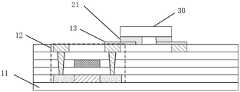
有鉴于此,本申请实施例提供了一种显示面板,如图1所示,该显示面板包括:In view of this, an embodiment of the present application provides a display panel, as shown in FIG. 1 , the display panel includes:
阵列基板,所述阵列基板包括基板11和位于所述基板11上的薄膜晶体管12和第一电极13,所述薄膜晶体管12和所述第一电极13电连接;an array substrate, the array substrate includes a
第一共晶单元21,所述第一共晶单元21位于所述阵列基板10上,且位于所述第一电极13远离所述基板11的一侧,通过所述第一电极13与所述薄膜晶体管12电连接;The first
发光单元30,所述发光单元30位于所述阵列基板上,通过所述第一共晶单元21与所述第一电极13电连接。The light-
具体工作时,所述第一电极和所述第一共晶单元电连接所述薄膜晶体管和所述发光单元,所述薄膜晶体管控制所述发光单元的发光状态。可选的,在本申请的一个实施例中,所示发光单元为Micro-led,但本申请对此并不做限定,具体视情况而定。During specific operation, the first electrode and the first eutectic unit are electrically connected to the thin film transistor and the light-emitting unit, and the thin-film transistor controls the light-emitting state of the light-emitting unit. Optionally, in an embodiment of the present application, the light-emitting unit shown is Micro-led, but this is not limited in the present application, and it depends on the situation.
具体的,所述显示面板在实际制作时,通常先在所述阵列基板上制作第一电极,再在所述第一电极上制作第一共晶单元,然后将发光单元转移到所述第一共晶单元远离所述第一电极的一侧,对所述发光单元和所述第一共晶单元的接触区域进行热压,以实现所述发光单元和所述第一共晶单元的电连接。Specifically, during the actual fabrication of the display panel, a first electrode is usually fabricated on the array substrate first, then a first eutectic unit is fabricated on the first electrode, and then the light-emitting unit is transferred to the first electrode. The side of the eutectic unit far away from the first electrode is hot-pressed on the contact area of the light-emitting unit and the first eutectic unit, so as to realize the electrical connection between the light-emitting unit and the first eutectic unit .
可选的,在本申请的一个实施例中,所述第一电极包括氧化铟锡电极,具体的,在本申请的一个实施例中,所述第一电极包括层叠的第一氧化铟锡电极、第一银电极和第二氧化铟锡电极,以使得所述第一电极具有较好的接触阻抗,但本申请对此并不做限定,具体视情况而定。Optionally, in an embodiment of the present application, the first electrode includes an indium tin oxide electrode. Specifically, in an embodiment of the present application, the first electrode includes a stacked first indium tin oxide electrode , a first silver electrode and a second indium tin oxide electrode, so that the first electrode has better contact resistance, but this application is not limited, and it depends on the situation.
需要说明的是,氧化铟锡熔点较低,质地较软,而如果所述第一电极的熔点较低,且质地较软,在对所述发光单元和所述第一共晶单元的接触区域进行热压时,会导致所述第一电极上表面塌陷、开裂,从而使得所述发光单元与所述第一电极电接触不良,影响所述发光单元的发光状态,使得所述显示面板出现暗点。It should be noted that the melting point of indium tin oxide is lower and the texture is softer, and if the melting point of the first electrode is lower and the texture is softer, in the contact area between the light-emitting unit and the first eutectic unit During hot pressing, the upper surface of the first electrode will collapse and crack, resulting in poor electrical contact between the light-emitting unit and the first electrode, affecting the light-emitting state of the light-emitting unit, and causing the display panel to appear dark. point.
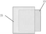
因此,在本申请的一个实施例中,如图2-图5所示,图2-图5为所述第一共晶单元和所述第一电极在所述基板上的投影的相对位置示意图,在本实施例中,所述第一共晶单元21在所述基板上的投影至少跨越所述第一电极13在所述基板上的投影的一个侧边,从而通过在垂直于所述基板的方向上,所述第一共晶单元21至少覆盖所述第一电极13的一个侧边,来降低所述第一电极13发生塌陷或开裂的风险,从而提升所述第一共晶单元21与所述第一电极13之间的电连接性能,进而提升所述第一电极13与薄膜晶体管12之间的电连接性能可靠性。Therefore, in an embodiment of the present application, as shown in FIG. 2-FIG. 5, FIG. 2-FIG. 5 are schematic diagrams of relative positions of the projection of the first eutectic unit and the first electrode on the substrate , in this embodiment, the projection of the
在上述实施例的基础上,在本申请的一个实施例中,所述第一共晶单元在所述基板上的投影至少跨越所述第一电极在所述基板的投影的一个侧边可以包括:如图2所示,所述第一共晶单元21在所述基板上的投影跨越所述第一电极13在所述基板上的投影的一个侧边,也可以包括:如图3和图4所示,所述第一共晶单元21在所述基板上的投影跨越所述第一电极13在所述基板上的投影的多个侧边,还可以包括:如图5所示,所述第一共晶单元21在所述基板上的投影跨越所述第一电极13在所述基板上的投影的各个侧边。本申请对此并不做限定,具体视情况而定。Based on the above embodiments, in an embodiment of the present application, the projection of the first eutectic unit on the substrate at least spans one side of the projection of the first electrode on the substrate may include: : As shown in FIG. 2 , the projection of the
需要说明的是,在上述实施例中,所述第一共晶单元在所述阵列基板上的投影至少跨越所述第一电极在所述阵列基板上的投影的一个侧边可以包括:如图6所示,所述第一共晶单元21与所述第一电极13的该侧边对应的侧面接触,也可以包括:如图7和图8所示,所述第一共晶单元21与所述第一电极13的该侧边对应的侧面不接触,本申请对此并不做限定,只要保证所述第一共晶单元在所述基板上的投影至少跨越所述第一电极在所述基板上的投影的一个侧边即可。It should be noted that, in the above embodiment, the projection of the first eutectic unit on the array substrate spans at least one side of the projection of the first electrode on the array substrate may include: 6, the
在上述实施例的基础上,在本申请的一个实施例中,如图9所示,所述第一电极13包括背离所述基板的第一表面131和与所述第一表面相连的侧面132,所述第一共晶单元21覆盖所述第一电极13的至少部分第一表面131和至少部分侧面132,从而使所述第一共晶单元21至少接触所述第一电极13侧面132的部分区域,来降低由于所述第一电极13上表面发生塌陷或开裂对所述第一共晶单元21与所述第一电极13之间电连接性能的影响,进而降低由于所述第一电极13上表面发生塌陷或开裂对所述第一电极13与所述发光单元30之间的电连接性能的影响。On the basis of the above embodiment, in an embodiment of the present application, as shown in FIG. 9 , the
可选的,在本申请的一个实施例中,如图5和图10所示,所述第一共晶单元21完全覆盖所述第一电极13裸露表面,具体的,所述第一电极13包括背离所述基板11的第一表面131和与所述第一表面131相连的侧面132,所述第一共晶单元21完全覆盖所述第一电极13的第一表面131和侧面132,从而最大程度的增大所述第一共晶单元21和所述第一电极13的接触面积,进而降低由于所述第一电极13发生塌陷或开裂对所述第一共晶单元21与所述第一电极13之间电连接性能的影响,最终降低由于所述第一电极13发生塌陷或开裂对所述第一电极13与所述发光单元30之间的电连接性能的影响。Optionally, in an embodiment of the present application, as shown in FIG. 5 and FIG. 10 , the
发明人研究发现,为了降低由于所述第一电极发生塌陷或开裂对所述第一电极与所述发光单元之间的电连接性能的影响,除了可以通过增加第一电极和所述第一共晶单元的接触面积,从而降低所述第一电极发生塌陷或开裂对所述第一电极与所述发光单元之间的电连接性能的影响外,还可以通过降低所述第一电极发生塌陷或开裂的概率,来提高所述第一电极和所述发光单元之间的电连接性能。The inventor found that, in order to reduce the influence on the electrical connection performance between the first electrode and the light-emitting unit due to the collapse or cracking of the first electrode, in addition to increasing the first electrode and the first common In addition to reducing the contact area of the crystal unit, the impact of the collapse or cracking of the first electrode on the electrical connection performance between the first electrode and the light-emitting unit can also be reduced by reducing the collapse or cracking of the first electrode. The probability of cracking is improved to improve the electrical connection performance between the first electrode and the light emitting unit.
因此,在本申请的一个实施例中,所述第一共晶单元的材料包括金和锡,以使得所述第一共晶单元具有较好的抗蠕变能力,从而利用所述第一共晶单元包裹住所述第一电极,来降低所述第一电极发生塌陷或开裂的概率,进而提高所述第一电极和所述发光单元之间的电连接性能。Therefore, in an embodiment of the present application, the material of the first eutectic unit includes gold and tin, so that the first eutectic unit has better creep resistance, so as to utilize the first eutectic unit The crystal unit wraps the first electrode to reduce the probability of collapse or cracking of the first electrode, thereby improving the electrical connection performance between the first electrode and the light-emitting unit.
在上述任一实施例的基础上,在本申请的一个实施例中,如图11和图12所示,所述阵列基板包括第一膜层14,所述第一膜层14位于所述第一电极13靠近所述基板11的一侧,所述第一膜层14设置第一凹槽(如图11所示)或者第一开口(如图12所示),所述第一共晶单元21包括填充所述第一凹槽或者所述第一开口的部分,从而通过将所述第一共晶单元21部分深入位于所述第一电极13靠近所述基板11一侧的第一膜层14中,来增加所述第一共晶单元21和所述第一膜层14之间的固定强度,进而提高所述第一共晶单元21对所述第一电极13的包覆性能,降低所述第一电极13发生塌陷或开裂的概率,提高所述发光单元30和所述第一电极13之间的电接触性能。On the basis of any of the above embodiments, in an embodiment of the present application, as shown in FIG. 11 and FIG. 12 , the array substrate includes a
可选的,在本申请的一个实施例中,如图13所示,图13为第一凹槽或第一开口、第一电极和第一共晶单元在基板上的投影的一种相对位置示意图,在本实施例中,所述第一凹槽或所述第一开口141在所述基板上的投影位于所述第一电极13位于所述基板上的投影的一侧,从而通过将所述第一共晶单元21部分从所述第一电极13的一侧深入所述第一膜层14中,增加所述第一共晶单元21和所述第一膜层14之间的固定强度,进而提高所述第一共晶单元21对所述第一电极13的包覆性能,并分散所述发光单元和所述第一共晶单元热压过程中,所述第一电极受到的压力,降低所述第一电极13发生塌陷或开裂的概率,提高所述发光单元和所述第一电极13之间的电接触性能。Optionally, in an embodiment of the present application, as shown in FIG. 13 , FIG. 13 is a relative position of the projection of the first groove or the first opening, the first electrode and the first eutectic unit on the substrate Schematic diagram, in this embodiment, the projection of the first groove or the
在本申请的另一个实施例中,如图14所示,图14为第一凹槽或第一开口、第一电极和第一共晶单元在基板上的投影的另一种相对位置示意图,在本实施例中,所述第一凹槽或所述第一开口141在所述基板上的投影位于所述第一电极13位于所述基板上的投影的相对的两侧,从而通过将所述第一共晶单元21部分从所述第一电极13相对的两侧一侧深入所述第一膜层14中,增加所述第一共晶单元21和所述第一膜层14之间的固定强度,进而提高所述第一共晶单元21对所述第一电极13的包覆性能,降低所述第一电极13发生塌陷或开裂的概率,提高所述发光单元和所述第一电极13之间的电接触性能。In another embodiment of the present application, as shown in FIG. 14 , FIG. 14 is another schematic diagram of relative positions of the projection of the first groove or the first opening, the first electrode and the first eutectic unit on the substrate, In this embodiment, the projection of the first groove or the
在本申请的又一个实施例中,如图15所示,图15为第一凹槽或第一开口、第一电极和第一共晶单元在基板上的投影的又一种相对位置示意图,在本实施例中,所述第一凹槽或所述第一开口141在所述基板上的投影位于所述第一电极13位于所述基板上的投影的相邻的两侧,从而通过将所述第一共晶单元21部分从所述第一电极13相邻的两侧深入所述第一膜层14中,增加所述第一共晶单元21和所述第一膜层14之间的固定强度,进而提高所述第一共晶单元21对所述第一电极13的包覆性能,降低所述第一电极13发生塌陷或开裂的概率,提高所述发光单元和所述第一电极13之间的电接触性能。In yet another embodiment of the present application, as shown in FIG. 15 , FIG. 15 is another schematic diagram of relative positions of the projection of the first groove or the first opening, the first electrode and the first eutectic unit on the substrate, In this embodiment, the projection of the first groove or the
在本申请的再一个实施例中,如图16所示,图16为第一凹槽或第一开口、第一电极和第一共晶单元在基板上的投影的再一种相对位置示意图,在本实施例中,所述第一凹槽或所述第一开口141在所述基板上的投影形状为环形,从而通过将所述第一共晶单元21部分从所述第一电极13的各侧深入所述第一膜层14中,来增加所述第一共晶单元21和所述第一膜层14之间的固定强度,进而提高所述第一共晶单元21对所述第一电极13的包覆性能,降低所述第一电极13发生塌陷或开裂的概率,提高所述发光单元和所述第一电极之间的电接触性能。在本申请的其他实施例中,所述第一凹槽或所述第一开口在所述阵列基板上的投影形状还可以为U形,如图17所示,本申请对此并不做限定,具体视情况而定。In still another embodiment of the present application, as shown in FIG. 16 , FIG. 16 is a schematic diagram of still another relative position of the projection of the first groove or the first opening, the first electrode and the first eutectic unit on the substrate, In this embodiment, the projected shape of the first groove or the
在上述任一实施例的基础上,在本申请的一个实施例中,如图7和图8所示,所述阵列基板包括第二膜层15,所述第二膜层15中设置有第二开口,所述第一电极13位于所述第二开口内。继续如图7和图8所示,在本实施例中,所述第二膜层15位于所述第一膜层14远离所述基板11的一侧,且所述第二膜层15中设置有第二开口,所述第一电极13位于所述第二开口内,且位于所述第一膜层14表面。On the basis of any of the above embodiments, in an embodiment of the present application, as shown in FIG. 7 and FIG. 8 , the array substrate includes a
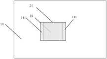
可选的,在本申请的一个实施例中,继续如图8所示,沿所述第一方向X,所述第二开口包括第一组成部分和第二组成部分,其中,所述第一组成部分位于所述第二组成部分朝向所述基板11的一侧,且所述第二组成部分在所述基板所在平面内的投影位于所述第一组成部分在所述基板所在平面的投影范围内。其中,所述第一方向X垂直于所述基板11所在平面。Optionally, in an embodiment of the present application, continuing as shown in FIG. 8 , along the first direction X, the second opening includes a first component and a second component, wherein the first The component is located on the side of the second component facing the
具体的,在上述实施例的基础上,在本申请的一个实施例中,继续如图8所示,所述第一电极13位于所述第二开口的第一组成部分,所述第一共晶单元21填充所述第二组成部分,以实现与所述第一电极13的电连接,可选的,所述第一共晶单元21部分位于所述第二开口的第二组成部分,部分位于所述第二膜层15表面。Specifically, on the basis of the above-mentioned embodiment, in an embodiment of the present application, as shown in FIG. 8 , the
图7和图8示意第二膜层15位于第一膜层14的远离基板11的一侧。在本发明的实施方式中,第二膜层15和第一膜层14可以为同一膜层,也即第二膜层(同第一膜层)制作于薄膜晶体管制作完成后,且设置第二开口,第二开口暴露薄膜晶体管的源极/漏极,第一电极13填充于第二开口内。7 and 8 illustrate that the
在上述实施例的基础上,在本申请的一个实施例中,继续如图8所示,所述第二组成部分在所述基板所在平面上的投影与所述第一组成部分在所述基板所在平面内的投影重合,具体的,所述第二开口在第二方向Y上的尺寸沿第一方向固定不变。其中,第一方向X垂直于所述基板所在平面,第二方向Y平行于所述基板所在平面。On the basis of the above embodiment, in an embodiment of the present application, as shown in FIG. 8 , the projection of the second component on the plane where the substrate is located is the same as the projection of the first component on the substrate The projections in the plane are coincident. Specifically, the size of the second opening in the second direction Y is fixed along the first direction. The first direction X is perpendicular to the plane where the substrate is located, and the second direction Y is parallel to the plane where the substrate is located.
在本申请的另一个实施例中,如图18所示,所述第二组成部分在所述基板所在平面的投影面积小于所述第一组成部分在所述基板所在平面的投影面积,具体的,所述第二组成部分在第二方向Y上的尺寸沿第一方向X固定不变,所述第一组成部分在第二方向Y上的尺寸沿第一方向X固定不变,所述第二组成部分在第二方向Y上的尺寸小于所述第一组成部分在第二方向Y上的尺寸。在本申请的其他实施例中,所述第二开口还可以采取其他结构,本申请对此并不做限定,具体视情况而定。In another embodiment of the present application, as shown in FIG. 18 , the projected area of the second component on the plane where the substrate is located is smaller than the projected area of the first component on the plane where the substrate is located. Specifically , the size of the second component in the second direction Y is fixed along the first direction X, the size of the first component in the second direction Y is fixed along the first direction X, the The dimension of the second component in the second direction Y is smaller than the dimension of the first component in the second direction Y. In other embodiments of the present application, the second opening may also adopt other structures, which are not limited in the present application, depending on the specific situation.
在上述任一实施例的基础上,在本申请的一个实施例中,如图19和图20所示,图19为所述第一电极在所述基板所在平面的投影示意图,图20为图19对应显示面板沿EF的剖视图,在本实施例中,所述第一电极13包括相互电连接的第一电极子部133,相邻的所述第一电极子部133之间具有第一间隙134,所述第一共晶单元21包括填充所述第一间隙134的部分,以通过利用所述第一共晶单元21部分填充所述第一电极13中相邻第一电极子部133之间的第一间隙134,来增大所述第一共晶单元21和所述第一电极13的接触面积以及所述第一共晶单元21和所述第一电极13之间的固定牢固度,降低由于所述第一电极13塌陷或开裂对所述第一电极13和所述发光单元30之间的电连接性能的影响。可选的,所述第一电极包括三个第一电极子部,以兼顾所述第一共晶单元和所述第一电极的接触面积以及所述第一电极的工艺难度,但本申请对此并不做限定,具体视情况而定。On the basis of any of the above embodiments, in an embodiment of the present application, as shown in FIGS. 19 and 20 , FIG. 19 is a schematic diagram of the projection of the first electrode on the plane where the substrate is located, and FIG. 20 is a diagram of 19 corresponds to the cross-sectional view of the display panel along EF. In this embodiment, the
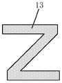
具体的,在上述实施例的基础上,在本申请的一个实施例中,所述第一电极13在所述基板所在平面内的投影形状为梳状,如图19所示;在本申请的另一个实施例中,所述第一电极13在所述基板所在平面内的投影形状为Z字形,如图21所示;在本申请的又一个实施例中,所述第一电极13在所述基板所在平面内的投影形状为辐射状,如图22所示;在本申请的其他实施例中,所述第一电极在所述阵列基板所在平面的投影形状还可以为其他形状,只要所述第一电极13由多个第一电极子部组成,且相邻第一电极子部之间具有第一间隙即可。Specifically, on the basis of the above embodiment, in an embodiment of the present application, the projected shape of the
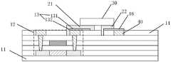
在上述任一实施例的基础上,在本申请的一个实施例中,如图23所示,所述薄膜晶体管包括:栅极121、第一极122和第二极123,其中,所述第一极122为源极和漏极中的一者,所述第二极123为源极和漏极中的另一者,即所述第一极122为源极时,所述第二极123为漏极,所述第一极123为漏极时,所述第二极122为源极。可选的,在本实施例中,所述第一共晶单元21通过所述第一电极12与所述薄膜晶体管的第一极122电连接。On the basis of any of the foregoing embodiments, in an embodiment of the present application, as shown in FIG. 23 , the thin film transistor includes: a
在上述实施例的基础上,在本申请的一个实施例中,继续如图23所示,所述显示面板还包括:阴极信号线40,所述阴极信号线40用于为所述发光单元30的负极提供电压信号。可选的,在本实施例中,所述阴极信号线40与所述第一极122位于同一层,以减小所述显示面板的厚度,更可选的,所述阴极信号线40与所述第一极122同时形成,从而在减小所述显示面板的厚度的基础上,简化所述显示面板的工艺流程。On the basis of the above-mentioned embodiment, in an embodiment of the present application, as shown in FIG. 23 , the display panel further includes: a
具体的,在上述实施例的基础上,在本申请的一个实施例中,继续如图23所示,所述阵列基板还包括第二电极16,相应的,所述显示面板还包括:第二共晶单元22,所述第二共晶单元22通过所述第二电极16与所述阴极信号线40电连接。Specifically, on the basis of the above-mentioned embodiment, in an embodiment of the present application, as shown in FIG. 23 , the array substrate further includes a
需要说明的是,在本实施例中,所述发光单元具有正极和负极,所述发光单元的正极通过所述第一共晶单元与所述第一电极电连接,所述发光单元的负极通过所述第二共晶单元与所述第二电极电连接,从而通过所述薄膜晶体管控制所述发光单元正极上的电压信号,通过所述阴极信号线控制所述发光单元负极上的电压信号。It should be noted that, in this embodiment, the light-emitting unit has a positive electrode and a negative electrode, the positive electrode of the light-emitting unit is electrically connected to the first electrode through the first eutectic unit, and the negative electrode of the light-emitting unit is connected to the first electrode through the first eutectic unit. The second eutectic unit is electrically connected to the second electrode, so that the voltage signal on the positive electrode of the light-emitting unit is controlled by the thin film transistor, and the voltage signal on the negative electrode of the light-emitting unit is controlled by the cathode signal line.
具体的,所述显示面板在实际制作时,通常先在所述阵列基板上制作第二电极,再在所述第二电极上制作第二共晶单元,然后将发光单元转移到所述第二共晶单元远离所述第二电极的一侧,对所述发光单元和所述第二共晶单元的接触区域进行热压,以实现所述发光单元和所述第二共晶单元的电连接。可选的,所述发光单元与所述第一共晶单元之间的热压过程和所述发光单元与所述第二共晶单元之间的热压过程同步进行,但本申请对此并不做限定,具体视情况而定。Specifically, when the display panel is actually fabricated, a second electrode is usually fabricated on the array substrate first, and then a second eutectic unit is fabricated on the second electrode, and then the light-emitting unit is transferred to the second electrode. the side of the eutectic unit away from the second electrode, and hot pressing the contact area between the light-emitting unit and the second eutectic unit, so as to realize the electrical connection between the light-emitting unit and the second eutectic unit . Optionally, the hot pressing process between the light emitting unit and the first eutectic unit and the hot pressing process between the light emitting unit and the second eutectic unit are performed simultaneously, but this application does not There is no limit, it depends on the situation.
可选的,在本申请的一个实施例中,所述第二电极包括氧化铟锡电极,具体的,在本申请的一个实施例中,所述第二电极包括层叠的第三氧化铟锡电极、第二银电极和第四氧化铟锡电极,以使得所述第二电极具有较好的接触阻抗,但本申请对此并不做限定,具体视情况而定。Optionally, in an embodiment of the present application, the second electrode includes an indium tin oxide electrode. Specifically, in an embodiment of the present application, the second electrode includes a stacked third indium tin oxide electrode , the second silver electrode and the fourth indium tin oxide electrode, so that the second electrode has better contact resistance, but this application is not limited, and it depends on the situation.
需要说明的是,氧化铟锡熔点较低,质地较软,而如果所述第二电极的熔点较低,且质地较软,在对所述发光单元和所述第二共晶单元的接触区域进行热压时,会导致所述第二电极上表面塌陷、开裂,从而使得所述发光单元与所述第二电极电接触不良,影响所述发光单元的发光状态,使得所述显示面板出现暗点。It should be noted that the melting point of indium tin oxide is lower and the texture is softer, and if the melting point of the second electrode is lower and the texture is softer, in the contact area between the light-emitting unit and the second eutectic unit During hot pressing, the upper surface of the second electrode will collapse and crack, resulting in poor electrical contact between the light-emitting unit and the second electrode, affecting the light-emitting state of the light-emitting unit, and causing the display panel to appear dark. point.
因此,在本申请的一个实施例中,所述第二共晶单元在所述基板上的投影至少跨越所述第二电极在所述基板上的投影的一个侧边,从而通过在垂直于所述基板的方向上,所述第二共晶单元至少覆盖所述第二电极的一个侧边,来降低由于所述第二电极发生塌陷或开裂对所述第二共晶单元与所述第二电极之间电连接性能的影响,进而降低由于所述第二电极发生塌陷或开裂对所述第二电极与所述发光单元之间的电连接性能的影响。Therefore, in an embodiment of the present application, the projection of the second eutectic unit on the substrate spans at least one side of the projection of the second electrode on the substrate, so that by being perpendicular to the substrate In the direction of the substrate, the second eutectic unit covers at least one side of the second electrode to reduce the impact on the second eutectic unit and the second electrode due to collapse or cracking of the second electrode. Influence on the electrical connection performance between the electrodes, thereby reducing the influence on the electrical connection performance between the second electrode and the light-emitting unit due to the collapse or cracking of the second electrode.
在上述实施例的基础上,在本申请的一个实施例中,所述第二共晶单元在所述基板上的投影至少跨越所述第二电极在所述基板的投影的一个侧边可以包括:所述第二共晶单元在所述基板上的投影跨越所述第二电极在所述基板上的投影的一个侧边,也可以包括:所述第二共晶单元在所述基板上的投影跨越所述第二电极在所述基板上的投影的多个侧边,还可以包括:所述第二共晶单元在所述基板上的投影跨越所述第二电极在所述基板上的投影的各个侧边。本申请对此并不做限定,具体视情况而定。On the basis of the above embodiments, in an embodiment of the present application, the projection of the second eutectic unit on the substrate at least spans one side of the projection of the second electrode on the substrate may include: : the projection of the second eutectic unit on the substrate spans one side of the projection of the second electrode on the substrate, and may also include: the projection of the second eutectic unit on the substrate The projection spans a plurality of sides of the projection of the second electrode on the substrate, and may further include: the projection of the second eutectic unit on the substrate spans the projection of the second electrode on the substrate The sides of the projection. This application does not limit this, depending on the specific situation.
需要说明的是,在上述实施例中,所述第二共晶单元在所述阵列基板上的投影至少跨越所述第二电极在所述阵列基板上的投影的一个侧边可以包括:如图6所示,所述第二共晶单元22与所述第二电极16的该侧边对应的侧面接触,也可以包括:如图7和图8所示,所述第二共晶单元22与所述第二电极16的该侧边对应的侧面不接触,本申请对此并不做限定,只要保证所述第二共晶单元在所述基板上的投影至少跨越所述第二电极在所述基板上的投影的一个侧边即可。It should be noted that, in the above embodiment, the projection of the second eutectic unit on the array substrate spans at least one side of the projection of the second electrode on the array substrate may include: As shown in FIG. 6, the
在上述实施例的基础上,在本申请的一个实施例中,如图9所示,所述第二电极16包括背离所述基板的第二表面161和与所述第二表面相连的侧面162,所述第二共晶单元22覆盖所述第二电极16的至少部分第二表面161和至少部分侧面162,从而使所述第二共晶单元22至少接触所述第二电极16侧面162的部分区域,来降低由于所述第二电极16上表面发生塌陷或开裂对所述第二共晶单元22与所述第二电极16之间电连接性能的影响,进而降低由于所述第二电极16上表面发生塌陷或开裂对所述第二电极16与所述发光单元30之间的电连接性能的影响。On the basis of the above embodiment, in an embodiment of the present application, as shown in FIG. 9 , the
可选的,在本申请的一个实施例中,如图10所示,所述第二共晶单元22完全覆盖所述第二电极16裸露表面,具体的,所述第二电极16包括背离所述基板11的第二表面161和与所述第二表面161相连的侧面162,所述第二共晶单元22完全覆盖所述第二电极16的第二表面161和侧面162,从而最大程度的增大所述第二共晶单元22和所述第二电极16的接触面积,进而降低由于所述第二电极16发生塌陷或开裂对所述第二共晶单元22与所述第二电极16之间电连接性能的影响,最终降低由于所述第二电极16发生塌陷或开裂对所述第二电极16与所述发光单元30之间的电连接性能的影响。Optionally, in an embodiment of the present application, as shown in FIG. 10 , the
发明人研究发现,为了降低由于所述第二电极发生塌陷或开裂对所述第二电极与所述发光单元之间的电连接性能的影响,除了可以通过增加第二电极和所述第二共晶单元的接触面积,从而降低所述第二电极发生塌陷或开裂对所述第二电极与所述发光单元之间的电连接性能的影响外,还可以通过降低所述第二电极发生塌陷或开裂的概率,来提高所述第二电极和所述发光单元之间的电连接性能。The inventor found that, in order to reduce the influence of the collapse or cracking of the second electrode on the electrical connection performance between the second electrode and the light-emitting unit, in addition to increasing the second electrode and the second common In addition to reducing the impact of the collapse or cracking of the second electrode on the electrical connection performance between the second electrode and the light-emitting unit, the contact area of the crystal unit can be reduced by reducing the collapse or cracking of the second electrode. The probability of cracking is improved to improve the electrical connection performance between the second electrode and the light emitting unit.
因此,在本申请的一个实施例中,所述第二共晶单元的材料包括金和锡,以使得所述第二共晶单元具有较好的抗蠕变能力,从而利用所述第二共晶单元包裹住所述第二电极,来降低所述第二电极发生塌陷或开裂的概率,进而提高所述第二电极和所述发光单元之间的电连接性能。Therefore, in an embodiment of the present application, the material of the second eutectic unit includes gold and tin, so that the second eutectic unit has better creep resistance, so as to utilize the second eutectic unit The crystal unit wraps the second electrode to reduce the probability of collapse or cracking of the second electrode, thereby improving the electrical connection performance between the second electrode and the light-emitting unit.
在上述任一实施例的基础上,在本申请的一个实施例中,如图11和图12所示,所述第一膜层14中还设置有第二凹槽(如图11所示)或者第三开口(如图12所示),所述第二共晶单元22包括填充所述第二凹槽或者所述第三开口的部分,从而通过将所述第二共晶单元22部分深入位于所述第二电极16靠近所述基板11一侧的第一膜层14中,来增加所述第二共晶单元22和所述第一膜层14之间的固定强度,进而提高所述第二共晶单元22对所述第二电极16的包覆性能,并分散所述发光单元和所述第二共晶单元的热压过程中,所述第二电极受到的压力,降低所述第二电极16发生塌陷或开裂的概率,提高所述发光单元30和所述第二电极16之间的电接触性能。On the basis of any of the above embodiments, in an embodiment of the present application, as shown in FIG. 11 and FIG. 12 , the
阵列基板中的第一膜层14可以于薄膜晶体管12制作完成后制作,第一膜层14的开口暴露薄膜晶体管的源极/漏极,用于与后续制作的第一电极13电连接。The
可选的,在本申请的一个实施例中,所述第二凹槽或所述第三开口在所述基板上的投影位于所述第二电极位于所述基板上的投影的一侧,从而通过将所述第二共晶单元部分从所述第二电极的一侧深入所述第一膜层中,增加所述第二共晶单元和所述第一膜层之间的固定强度,进而提高所述第二共晶单元对所述第二电极的包覆性能,降低所述第二电极发生塌陷或开裂的概率,提高所述发光单元和所述第二电极之间的电接触性能。Optionally, in an embodiment of the present application, the projection of the second groove or the third opening on the substrate is located on the side of the projection of the second electrode on the substrate, so that By inserting the second eutectic unit part into the first film layer from one side of the second electrode, the fixing strength between the second eutectic unit and the first film layer is increased, and further The coating performance of the second eutectic unit on the second electrode is improved, the probability of collapse or cracking of the second electrode is reduced, and the electrical contact performance between the light-emitting unit and the second electrode is improved.
在本申请的另一个实施例中,所述第二凹槽或所述第三开口在所述基板上的投影位于所述第二电极位于所述基板上的投影的相对的两侧,从而通过将所述第二共晶单元部分从所述第一电极相对的两侧一侧深入所述第一膜层中,增加所述第二共晶单元和所述第一膜层之间的固定强度,进而提高所述第二共晶单元对所述第二电极的包覆性能,降低所述第二电极发生塌陷或开裂的概率,提高所述发光单元和所述第二电极之间的电接触性能。In another embodiment of the present application, the projection of the second groove or the third opening on the substrate is located on opposite sides of the projection of the second electrode on the substrate, so as to pass Parts of the second eutectic unit are penetrated into the first film layer from opposite sides of the first electrode to increase the fixing strength between the second eutectic unit and the first film layer , thereby improving the coating performance of the second eutectic unit on the second electrode, reducing the probability of collapse or cracking of the second electrode, and improving the electrical contact between the light-emitting unit and the second electrode performance.
在本申请的又一个实施例中,所述第二凹槽或所述第三开口在所述基板上的投影位于所述第二电极位于所述基板上的投影的相邻的两侧,从而通过将所述第二共晶单元部分从所述第二电极相邻的两侧深入所述第一膜层中,增加所述第二共晶单元和所述第一膜层之间的固定强度,进而提高所述第二共晶单元对所述第二电极的包覆性能,降低所述第二电极发生塌陷或开裂的概率,提高所述发光单元和所述第二电极之间的电接触性能。In yet another embodiment of the present application, the projection of the second groove or the third opening on the substrate is located on two adjacent sides of the projection of the second electrode on the substrate, so that The fixing strength between the second eutectic unit and the first film layer is increased by inserting the second eutectic unit part into the first film layer from the adjacent two sides of the second electrode , thereby improving the coating performance of the second eutectic unit on the second electrode, reducing the probability of collapse or cracking of the second electrode, and improving the electrical contact between the light-emitting unit and the second electrode performance.
在本申请的再一个实施例中,所述第二凹槽或所述第三开口在所述基板上的投影形状为环形,从而通过将所述第二共晶单元部分从所述第二电极的各侧深入所述第一膜层中,来增加所述第二共晶单元和所述第一膜层之间的固定强度,进而提高所述第二共晶单元对所述第二电极的包覆性能,降低所述第二电极发生塌陷或开裂的概率,提高所述发光单元和所述第二电极之间的电接触性能。在本申请的其他实施例中,所述第二凹槽或所述第三开口在所述阵列基板上的投影形状还可以为U形,本申请对此并不做限定,具体视情况而定。In still another embodiment of the present application, the projection shape of the second groove or the third opening on the substrate is a ring shape, so that the second eutectic unit is partially separated from the second electrode by the second eutectic unit. Each side of the electrode penetrates deep into the first film layer to increase the fixing strength between the second eutectic unit and the first film layer, thereby improving the adhesion of the second eutectic unit to the second electrode. The coating performance reduces the probability of collapse or cracking of the second electrode, and improves the electrical contact performance between the light-emitting unit and the second electrode. In other embodiments of the present application, the projected shape of the second groove or the third opening on the array substrate may also be a U-shape, which is not limited in the present application, and depends on the situation. .
在上述任一实施例的基础上,在本申请的一个实施例中,如图7和图8所示,所述第二膜层15中还设置有第四开口,所述第二电极16位于所述第四开口内。继续如图7和图8所示,在本实施例中,所述第二膜层15位于所述第一膜层14远离所述基板11的一侧,且所述第二膜层15中设置有第四开口,所述第二电极16位于所述第四开口内,且位于所述第一膜层14表面。On the basis of any of the above embodiments, in an embodiment of the present application, as shown in FIG. 7 and FIG. 8 , the
可选的,在本申请的一个实施例中,继续如图8所示,沿所述第一方向X,所述第四开口包括第三组成部分和第四组成部分,其中,所述第三组成部分位于所述第四组成部分朝向所述基板11的一侧,且所述第四组成部分在所述基板所在平面内的投影位于所述第三组成部分在所述基板所在平面的投影范围内。其中,所述第一方向X垂直于所述基板11所在平面。Optionally, in an embodiment of the present application, as shown in FIG. 8 , along the first direction X, the fourth opening includes a third component and a fourth component, wherein the third The component is located on the side of the fourth component facing the
具体的,在上述实施例的基础上,在本申请的一个实施例中,继续如图8所示,所述第二电极16位于所述第四开口的第三组成部分,所述第二共晶单元22填充所述第四组成部分,以实现与所述第二电极16的电连接,可选的,所述第二共晶单元22部分位于所述第四开口的第四组成部分,部分位于所述第二膜层15表面。Specifically, on the basis of the above-mentioned embodiment, in an embodiment of the present application, as shown in FIG. 8 , the
在上述实施例的基础上,在本申请的一个实施例中,继续如图8所示,所述第四组成部分在所述基板所在平面上的投影与所述第三组成部分在所述基板所在平面内的投影重合,具体的,所述第四开口在第二方向Y上的尺寸沿第一方向固定不变。其中,第一方向X垂直于所述基板所在平面,第二方向Y平行于所述基板所在平面。On the basis of the above embodiment, in an embodiment of the present application, as shown in FIG. 8 , the projection of the fourth component on the plane where the substrate is located is the same as the projection of the third component on the substrate The projections in the plane are coincident. Specifically, the size of the fourth opening in the second direction Y is fixed along the first direction. The first direction X is perpendicular to the plane where the substrate is located, and the second direction Y is parallel to the plane where the substrate is located.
在本申请的另一个实施例中,如图18所示,所述第四组成部分在所述基板所在平面的投影面积小于所述第三组成部分在所述基板所在平面的投影面积,具体的,所述第四组成部分在第二方向Y上的尺寸沿第一方向X固定不变,所述第三组成部分在第二方向Y上的尺寸沿第一方向X固定不变,所述第四组成部分在第二方向Y上的尺寸小于所述第三组成部分在第二方向Y上的尺寸。在本申请的其他实施例中,所述第四开口还可以采取其他结构,本申请对此并不做限定,具体视情况而定。In another embodiment of the present application, as shown in FIG. 18 , the projected area of the fourth component on the plane where the substrate is located is smaller than the projected area of the third component on the plane where the substrate is located. Specifically , the size of the fourth component in the second direction Y is fixed along the first direction X, the size of the third component in the second direction Y is fixed along the first direction X, the The dimension of the fourth component in the second direction Y is smaller than the dimension of the third component in the second direction Y. In other embodiments of the present application, the fourth opening may also adopt other structures, which are not limited in the present application, depending on the situation.
在上述任一实施例的基础上,在本申请的一个实施例中,如图20所示,在本实施例中,所述第二电极16包括相互电连接的第二电极子部163,相邻的所述第二电极子部163之间具有第二间隙164,所述第二共晶单元22包括填充所述第二间隙164的部分,以通过利用所述第二共晶单元22部分填充所述第二电极16中相邻第二电极子部163之间的第二间隙164,来增大所述第二共晶单元22和所述第二电极16的接触面积以及所述第二共晶单元22和所述第二电极16之间的固定牢固度,降低由于所述第二电极16塌陷或开裂对所述第二电极16和所述发光单元30之间的电连接性能的影响。可选的,所述第二电极包括三个第二电极子部,以兼顾所述第二共晶单元和所述第二电极的接触面积以及所述第二电极的工艺难度,但本申请对此并不做限定,具体视情况而定。On the basis of any of the above embodiments, in an embodiment of the present application, as shown in FIG. 20 , in this embodiment, the
具体的,在上述实施例的基础上,在本申请的一个实施例中,所述第二电极在所述基板所在平面内的投影形状为梳状;在本申请的另一个实施例中,所述第二电极在所述基板所在平面内的投影形状为Z字形;在本申请的又一个实施例中,所述第二电极在所述基板所在平面内的投影形状为辐射状;在本申请的其他实施例中,所述第二电极在所述阵列基板所在平面的投影形状还可以为其他形状,只要所述第二电极16由多个第二电极子部组成,且相邻第二电极子部之间具有第二间隙即可。Specifically, on the basis of the above-mentioned embodiment, in an embodiment of the present application, the projected shape of the second electrode in the plane where the substrate is located is a comb shape; in another embodiment of the present application, the The projected shape of the second electrode on the plane where the substrate is located is a zigzag shape; in another embodiment of the present application, the projected shape of the second electrode on the plane where the substrate is located is a radial shape; in the present application In other embodiments, the projected shape of the second electrode on the plane where the array substrate is located can also be other shapes, as long as the
在上述实施例的基础上,在本申请的一个实施例中,如图24所示,所述第一共晶单元21覆盖所述第一极122远离所述阴极信号线40一侧部分表面,所述第二共晶单元22覆盖所述阴极信号线40远离所述第一极122一侧至少部分表面,从而使得所述第一共晶单元21和所述第二共晶单元22不位于所述第一极122和所述阴极信号线40之间,进而保证所述第一极122和所述阴极信号线40之间具有足够的绝缘距离,避免所述第一极122和所述阴极信号线40短路,影响所述发光单元的工作状态。On the basis of the above embodiment, in an embodiment of the present application, as shown in FIG. 24 , the
另外,所述第一共晶单元覆盖所述第一极远离所述阴极信号线一侧部分表面,还可以保证所述第一共晶单元覆盖所述第一极远离所述阴极信号线一侧与所述第一电极的接触区域,从而降低所述第一极和所述第一电极的接触区域边界发生开裂的概率,降低所述第一极和所述第一电极的接触电阻;同理,所述第二共晶单元覆盖所述阴极信号线远离所述第一极一侧至少部分表面,还可以保证所述第二共晶单元覆盖所述阴极信号线远离所述第一极一侧与所述第二电极的接触区域,从而降低所述第二电极和所述阴极信号线的接触区域边界发生开裂的概率,降低所述第二电极和所述阴极信号线的接触电阻。In addition, the first eutectic unit covers a part of the surface of the first electrode away from the cathode signal line, which can also ensure that the first eutectic unit covers the side of the first electrode away from the cathode signal line The contact area with the first electrode, thereby reducing the probability of cracking in the boundary of the contact area between the first electrode and the first electrode, and reducing the contact resistance between the first electrode and the first electrode; the same is true , the second eutectic unit covers at least part of the surface of the cathode signal line away from the first pole, and can also ensure that the second eutectic unit covers the cathode signal line away from the first pole side The contact area with the second electrode, thereby reducing the probability of cracking at the boundary of the contact area between the second electrode and the cathode signal line, and reducing the contact resistance between the second electrode and the cathode signal line.
此外,本申请实施例还提供了一种显示装置,如图25所示,该显示装置包括上述任一实施例所提供的显示面板。可选的,所述显示装置可以为手机、平板电脑、电视等各种具有显示面板的设备,本申请对此并不做限定,具体视情况而定。In addition, an embodiment of the present application further provides a display device. As shown in FIG. 25 , the display device includes the display panel provided by any of the above-mentioned embodiments. Optionally, the display device may be various devices having a display panel, such as a mobile phone, a tablet computer, a TV, etc., which is not limited in this application, depending on the specific situation.
综上,本申请实施例所提供的显示面板以及包括该显示面板的显示装置中,可以降低由于所述第一电极发生塌陷或开裂对所述第一电极与所述发光单号之间电接触性能的影响,从而提高所述发光单元和所述第一电极之间的电接触性能,降低所述显示面板和所述显示装置出现暗点的概率。In conclusion, in the display panel and the display device including the display panel provided by the embodiments of the present application, the electrical contact between the first electrode and the light-emitting unit due to the collapse or cracking of the first electrode can be reduced Therefore, the electrical contact performance between the light-emitting unit and the first electrode is improved, and the probability of dark spots appearing on the display panel and the display device is reduced.
对所公开的实施例的上述说明,使本领域专业技术人员能够实现或使用本申请。对这些实施例的多种修改对本领域的专业技术人员来说将是显而易见的,本文中所定义的一般原理可以在不脱离本申请的精神或范围的情况下,在其它实施例中实现。因此,本申请将不会被限制于本文所示的这些实施例,而是要符合与本文所公开的原理和新颖特点相一致的最宽的范围。The above description of the disclosed embodiments enables any person skilled in the art to make or use the present application. Various modifications to these embodiments will be readily apparent to those skilled in the art, and the generic principles defined herein may be implemented in other embodiments without departing from the spirit or scope of the present application. Therefore, this application is not intended to be limited to the embodiments shown herein, but is to be accorded the widest scope consistent with the principles and novel features disclosed herein.
Claims (12)
Translated fromChinesePriority Applications (1)
| Application Number | Priority Date | Filing Date | Title |
|---|---|---|---|
| CN202210230493.2ACN114613899A (en) | 2022-03-09 | 2022-03-09 | Display panel and display device |
Applications Claiming Priority (1)
| Application Number | Priority Date | Filing Date | Title |
|---|---|---|---|
| CN202210230493.2ACN114613899A (en) | 2022-03-09 | 2022-03-09 | Display panel and display device |
Publications (1)
| Publication Number | Publication Date |
|---|---|
| CN114613899Atrue CN114613899A (en) | 2022-06-10 |
Family
ID=81860342
Family Applications (1)
| Application Number | Title | Priority Date | Filing Date |
|---|---|---|---|
| CN202210230493.2APendingCN114613899A (en) | 2022-03-09 | 2022-03-09 | Display panel and display device |
Country Status (1)
| Country | Link |
|---|---|
| CN (1) | CN114613899A (en) |
Citations (12)
| Publication number | Priority date | Publication date | Assignee | Title |
|---|---|---|---|---|
| US20110273410A1 (en)* | 2010-05-07 | 2011-11-10 | Snu R&Db Foundation | Led display apparatus having active devices and fabrication method thereof |
| JP2012204572A (en)* | 2011-03-25 | 2012-10-22 | Murata Mfg Co Ltd | Chip component structure |
| CN203950832U (en)* | 2014-04-15 | 2014-11-19 | 严敏 | A kind of small size semiconductor LED eutectic wafer |
| CN104995703A (en)* | 2013-02-18 | 2015-10-21 | 太阳诱电株式会社 | Multilayer ceramic capacitor with interposer, and interposer for multilayer ceramic capacitor |
| WO2016111243A1 (en)* | 2015-01-07 | 2016-07-14 | Nttエレクトロニクス株式会社 | Flexible printed wiring board and mounting method for same |
| CN107623012A (en)* | 2016-07-13 | 2018-01-23 | 群创光电股份有限公司 | Display device and method for forming same |
| CN107742636A (en)* | 2017-10-25 | 2018-02-27 | 上海天马微电子有限公司 | Display panel and display device |
| CN107978582A (en)* | 2016-10-25 | 2018-05-01 | 矽创电子股份有限公司 | Chip packaging structure and related pin bonding method |
| CN112151568A (en)* | 2019-06-28 | 2020-12-29 | 群创光电股份有限公司 | Electronic device |
| US20210110761A1 (en)* | 2019-10-15 | 2021-04-15 | Boe Technology Group Co., Ltd. | Driving backplane, display panel and method for manufacturing the same |
| US10985187B1 (en)* | 2019-12-31 | 2021-04-20 | Shanghai Tianma Micro-electronics Co., Ltd. | Display panel and fabrication method, and display device |
| CN112786640A (en)* | 2020-12-30 | 2021-05-11 | 厦门天马微电子有限公司 | Array substrate, preparation method thereof, display panel and display device |
- 2022
- 2022-03-09CNCN202210230493.2Apatent/CN114613899A/enactivePending
Patent Citations (12)
| Publication number | Priority date | Publication date | Assignee | Title |
|---|---|---|---|---|
| US20110273410A1 (en)* | 2010-05-07 | 2011-11-10 | Snu R&Db Foundation | Led display apparatus having active devices and fabrication method thereof |
| JP2012204572A (en)* | 2011-03-25 | 2012-10-22 | Murata Mfg Co Ltd | Chip component structure |
| CN104995703A (en)* | 2013-02-18 | 2015-10-21 | 太阳诱电株式会社 | Multilayer ceramic capacitor with interposer, and interposer for multilayer ceramic capacitor |
| CN203950832U (en)* | 2014-04-15 | 2014-11-19 | 严敏 | A kind of small size semiconductor LED eutectic wafer |
| WO2016111243A1 (en)* | 2015-01-07 | 2016-07-14 | Nttエレクトロニクス株式会社 | Flexible printed wiring board and mounting method for same |
| CN107623012A (en)* | 2016-07-13 | 2018-01-23 | 群创光电股份有限公司 | Display device and method for forming same |
| CN107978582A (en)* | 2016-10-25 | 2018-05-01 | 矽创电子股份有限公司 | Chip packaging structure and related pin bonding method |
| CN107742636A (en)* | 2017-10-25 | 2018-02-27 | 上海天马微电子有限公司 | Display panel and display device |
| CN112151568A (en)* | 2019-06-28 | 2020-12-29 | 群创光电股份有限公司 | Electronic device |
| US20210110761A1 (en)* | 2019-10-15 | 2021-04-15 | Boe Technology Group Co., Ltd. | Driving backplane, display panel and method for manufacturing the same |
| US10985187B1 (en)* | 2019-12-31 | 2021-04-20 | Shanghai Tianma Micro-electronics Co., Ltd. | Display panel and fabrication method, and display device |
| CN112786640A (en)* | 2020-12-30 | 2021-05-11 | 厦门天马微电子有限公司 | Array substrate, preparation method thereof, display panel and display device |
Similar Documents
| Publication | Publication Date | Title |
|---|---|---|
| CN111755463A (en) | Display panel and display device | |
| TWI307978B (en) | Cascade organic electroluminescent device | |
| EP1646092A3 (en) | Contact and omni directional reflective mirror for flip chipped light emitting devices | |
| CN111312742A (en) | Backlight module, preparation method thereof and display device | |
| CN111625119B (en) | Touch screen and display device | |
| CN112257524B (en) | Fingerprint identification display panel and fingerprint identification display device | |
| CN108878677B (en) | Display panel and display device | |
| CN110112205A (en) | Display base plate and its manufacturing method, organic LED display device | |
| CN102569341A (en) | Organic light emitting diode display | |
| CN115835687A (en) | Display panel and display device | |
| CN110970477B (en) | Organic light emitting display panel and display device | |
| WO2023246261A1 (en) | Display panel and display device | |
| US20250212621A1 (en) | Display panel, display apparatus, and method for manufacturing display panel | |
| US20220020907A1 (en) | Display device, display screen and method for manufacturing display device | |
| CN101834200B (en) | Organic RL display and fabricating method thereof | |
| WO2023103101A1 (en) | Oled display panel and display apparatus | |
| CN111933671B (en) | Display substrate, manufacturing method thereof and display panel | |
| WO2025161917A1 (en) | Display panel and manufacturing method therefor, and display apparatus | |
| CN113327940B (en) | Display panel, manufacturing method thereof and display device | |
| CN114613899A (en) | Display panel and display device | |
| CN118201401A (en) | Display panel and display device | |
| US20250081774A1 (en) | Display substrate, display device, and display substrate manufacturing method | |
| CN216015371U (en) | Display panel and display device | |
| CN109686767A (en) | Display device and its manufacturing method | |
| CN108615734A (en) | Display panel and preparation method thereof, display device |
Legal Events
| Date | Code | Title | Description |
|---|---|---|---|
| PB01 | Publication | ||
| PB01 | Publication | ||
| SE01 | Entry into force of request for substantive examination | ||
| SE01 | Entry into force of request for substantive examination |