CN114597660B - Antenna of multilayer mixed plasma nano patch - Google Patents
Antenna of multilayer mixed plasma nano patchDownload PDFInfo
- Publication number
- CN114597660B CN114597660BCN202210220595.6ACN202210220595ACN114597660BCN 114597660 BCN114597660 BCN 114597660BCN 202210220595 ACN202210220595 ACN 202210220595ACN 114597660 BCN114597660 BCN 114597660B
- Authority
- CN
- China
- Prior art keywords
- layer
- antenna
- patch
- silicon dioxide
- metal layer
- Prior art date
- Legal status (The legal status is an assumption and is not a legal conclusion. Google has not performed a legal analysis and makes no representation as to the accuracy of the status listed.)
- Active
Links
Images


Classifications
- H—ELECTRICITY
- H01—ELECTRIC ELEMENTS
- H01Q—ANTENNAS, i.e. RADIO AERIALS
- H01Q9/00—Electrically-short antennas having dimensions not more than twice the operating wavelength and consisting of conductive active radiating elements
- H01Q9/04—Resonant antennas
- H01Q9/0407—Substantially flat resonant element parallel to ground plane, e.g. patch antenna
- H—ELECTRICITY
- H01—ELECTRIC ELEMENTS
- H01Q—ANTENNAS, i.e. RADIO AERIALS
- H01Q1/00—Details of, or arrangements associated with, antennas
- H01Q1/002—Protection against seismic waves, thermal radiation or other disturbances, e.g. nuclear explosion; Arrangements for improving the power handling capability of an antenna
- H—ELECTRICITY
- H01—ELECTRIC ELEMENTS
- H01Q—ANTENNAS, i.e. RADIO AERIALS
- H01Q1/00—Details of, or arrangements associated with, antennas
- H01Q1/27—Adaptation for use in or on movable bodies
- H01Q1/34—Adaptation for use in or on ships, submarines, buoys or torpedoes
- H—ELECTRICITY
- H01—ELECTRIC ELEMENTS
- H01Q—ANTENNAS, i.e. RADIO AERIALS
- H01Q1/00—Details of, or arrangements associated with, antennas
- H01Q1/36—Structural form of radiating elements, e.g. cone, spiral, umbrella; Particular materials used therewith
- H01Q1/364—Structural form of radiating elements, e.g. cone, spiral, umbrella; Particular materials used therewith using a particular conducting material, e.g. superconductor
Landscapes
- Waveguide Aerials (AREA)
Abstract
Translated fromChinese
Description
Translated fromChinese技术领域Technical Field
本发明属于通信技术领域,更进一步涉及电磁场与微波技术领域中的一种多层混合等离子体纳米贴片的天线。本发明可用于在满足天线宽带化的情况下,适用于标准通信波长的下的无线传输的天线。The present invention belongs to the field of communication technology, and further relates to a multi-layer hybrid plasma nanopatch antenna in the field of electromagnetic field and microwave technology. The present invention can be used for an antenna suitable for wireless transmission at a standard communication wavelength while satisfying the requirement of antenna broadbandization.
背景技术Background Art
纳米天线因其在纳米尺度控制、操作和辐射光线的特性,而被广泛地应用在无线通信技术领域。光学纳米天线是在亚波长尺度上对光频段电磁波进行调控,实现近场局域光场和远场辐射光场的自由转换。在设计光学纳米天线时,往往基于表面等离激元理论,利用其“尖端效应”来实现的。现有技术的纳米天线主要基于纯等离激元,由于过度的欧姆损耗而导致天线效率非常低且没有良好的远场特性。在实际应用的时候纳米天线往往阻抗较大,并且表面等离激元损耗很大,从而在天线的效率性能等方面带来一些不利因素。Nanoantennas are widely used in the field of wireless communication technology because of their ability to control, manipulate and radiate light at the nanoscale. Optical nanoantennas regulate electromagnetic waves in the optical frequency band on a subwavelength scale to achieve free conversion between near-field localized light fields and far-field radiated light fields. When designing optical nanoantennas, they are often based on surface plasmon theory and use its "tip effect" to achieve this. Nanoantennas in the prior art are mainly based on pure plasmons, which have very low antenna efficiency and no good far-field characteristics due to excessive ohmic losses. In actual applications, nanoantennas often have large impedances and large surface plasmon losses, which brings some disadvantages in terms of antenna efficiency and performance.
Zahra Manzoor等人在其发表的论文“E-shaped Nano-antenna with AsymmetricIntegrated Dielectric-plasmonic Waveguide”(IEEE International Symposium onAntennas and Propagation and USNC-URSI Radio Science Meeting.2019年)中提出了一种非对称集成的E型纳米混合等离子体天线。该天线包括单层介质波导和非对称集成介质-等离子体纳米天线,通过锥形耦合器将该单层介质波导与非对称集成介质连接成E型等离子体纳米天线。其中单层介质波导由二氧化硅、硅和氮化硅材料组成,非对称集成介质由银和二氧化硅材料组成,波导作为纳米天线的一部分采用开放式连接,减小了连接损耗,有利于表面等离激元传播的距离更远。但是,该天线仍然存在的不足之处是,该天线为单层绝缘层介质天线,导致天线表面等离子体的传播损耗大。Zahra Manzoor et al. proposed an asymmetric integrated E-shaped nano-hybrid plasma antenna in their paper "E-shaped Nano-antenna with Asymmetric Integrated Dielectric-plasmonic Waveguide" (IEEE International Symposium on Antennas and Propagation and USNC-URSI Radio Science Meeting. 2019). The antenna includes a single-layer dielectric waveguide and an asymmetric integrated dielectric-plasmonic nanoantenna, and the single-layer dielectric waveguide is connected to the asymmetric integrated dielectric through a conical coupler to form an E-type plasma nanoantenna. The single-layer dielectric waveguide is composed of silicon dioxide, silicon and silicon nitride materials, and the asymmetric integrated dielectric is composed of silver and silicon dioxide materials. The waveguide, as part of the nanoantenna, adopts an open connection, which reduces the connection loss and is conducive to the propagation of surface plasmons over a longer distance. However, the antenna still has the disadvantage that the antenna is a single-layer insulating layer dielectric antenna, which leads to large propagation losses of the antenna surface plasma.
Abbas Nourmohammadi等人在其发表的论文“Ultra-Wideband Photonic HybridPlasmonic Horn Nanoantenna with SOI Configuration”(Silicon(2020)12:193–198)中公开了一种超宽带光子混合等离子体喇叭纳米天线。该纳米天线包括一个基于SOI的混合等离子体单层介质波导和喇叭天线。其中基于SOI的混合等离子体单层介质波导和喇叭天线的材料都由金、二氧化硅和硅材料组成,基地上的波导与喇叭天线直接相连为一个整体,减小了连接损耗,有利于天线在较宽的频率范围内工作。但是,该天线仍然存在的不足之处是,该天线基于SOI的混合等离子体波导的介质为单层,且材料金电阻率很大,导致天线表面金属层电阻很大。Abbas Nourmohammadi et al. disclosed an ultra-wideband photonic hybrid plasma horn nanoantenna in their published paper "Ultra-Wideband Photonic Hybrid Plasmonic Horn Nanoantenna with SOI Configuration" (Silicon (2020) 12: 193–198). The nanoantenna includes a hybrid plasma single-layer dielectric waveguide based on SOI and a horn antenna. The materials of the hybrid plasma single-layer dielectric waveguide and the horn antenna based on SOI are both composed of gold, silicon dioxide and silicon materials. The waveguide on the base is directly connected to the horn antenna as a whole, which reduces the connection loss and is conducive to the antenna working in a wider frequency range. However, the antenna still has the disadvantage that the medium of the hybrid plasma waveguide based on SOI is a single layer, and the resistivity of the gold material is very large, resulting in a large resistance of the metal layer on the surface of the antenna.
发明内容Summary of the invention
本发明的目的在于针对上述现有技术存在的不足,提出了一种多层混合等离子体的纳米贴片天线,旨在解决天线表面等离子体的传播损耗大和天线表面金属层阻抗很大的问题。The purpose of the present invention is to address the deficiencies of the above-mentioned prior art and propose a multi-layer hybrid plasma nanopatch antenna, aiming to solve the problems of large propagation loss of antenna surface plasma and large impedance of the metal layer on the antenna surface.
实现本发明目的的具体思路是:本发明的基底上设置的混合等离子体波导和贴片均采用双层介质层,由于双层介质层使得天线的表面等离子体更多的传播,以此解决天线表面等离子体的传播损耗大的问题。本发明的混合等离子体波导和贴片均采用单层银金属层,由于银的电阻率低的金属材料电阻更低,而满足天线性能且电阻率更低的金属材料作为天线表面的金属层,可以解决天线表面金属层阻抗大的问题。The specific idea of achieving the purpose of the present invention is: the hybrid plasma waveguide and patch arranged on the substrate of the present invention both use a double-layer dielectric layer, because the double-layer dielectric layer allows the surface plasma of the antenna to propagate more, thereby solving the problem of large propagation loss of the antenna surface plasma. The hybrid plasma waveguide and patch of the present invention both use a single-layer silver metal layer, because the metal material with low resistivity of silver has lower resistance, and the metal material that meets the antenna performance and has lower resistivity is used as the metal layer on the surface of the antenna, which can solve the problem of large impedance of the metal layer on the surface of the antenna.
为实现上述目的,本发明的技术方案如下:To achieve the above object, the technical solution of the present invention is as follows:
本发明的多层混合等离子体纳米贴片的天线,包括依次设置在基底上的混合等离子体波导和贴片。混合等离子体波导和贴片均由双层二氧化硅介质层、单层硅绝缘层和单层银金属层构成;所述贴片为多面体结构;所述基底由单层硅绝缘层和单层银金属层构成。The multi-layer hybrid plasma nanopatch antenna of the present invention comprises a hybrid plasma waveguide and a patch sequentially arranged on a substrate. The hybrid plasma waveguide and the patch are both composed of a double-layer silicon dioxide dielectric layer, a single-layer silicon insulating layer and a single-layer silver metal layer; the patch is a polyhedral structure; and the substrate is composed of a single-layer silicon insulating layer and a single-layer silver metal layer.
本发明与现有技术相比具有以下优点:Compared with the prior art, the present invention has the following advantages:
第一,由于本发明的天线的混合等离子体波导由双层二氧化硅介质层、单层硅绝缘层和单层银金属层构成,克服了现有技术天线表面等离子体传播损耗大的缺陷,使得本发明具有更高的天线辐射效率的优点。First, since the hybrid plasma waveguide of the antenna of the present invention is composed of a double-layer silicon dioxide dielectric layer, a single-layer silicon insulating layer and a single-layer silver metal layer, it overcomes the defect of large surface plasma propagation loss of the antenna in the prior art, so that the present invention has the advantage of higher antenna radiation efficiency.
第二,由于本发明的混合等离子体波导和贴片均由单层银金属层构成,克服了现有技术天线的表面金属层阻抗很大的不足,使得本发明具有更好的阻抗匹配的优点。Secondly, since the hybrid plasma waveguide and patch of the present invention are both composed of a single silver metal layer, the disadvantage of the large impedance of the surface metal layer of the antenna in the prior art is overcome, so that the present invention has the advantage of better impedance matching.
附图说明BRIEF DESCRIPTION OF THE DRAWINGS
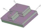
图1是本发明的整体结构示意图;Fig. 1 is a schematic diagram of the overall structure of the present invention;
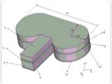
图2是本发明实施例中混合等离子体波导和贴片结构的示意图;FIG2 is a schematic diagram of a hybrid plasma waveguide and patch structure in an embodiment of the present invention;
图3是本发明实施例中基底结构的示意图;FIG3 is a schematic diagram of a substrate structure according to an embodiment of the present invention;
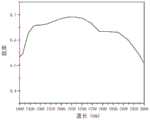
图4是本发明仿真实验的天线回波损耗特性S11图;FIG4 is a graph of antenna return loss characteristics S11 of a simulation experiment of the present invention;
图5是本发明仿真实验的天线效率图;FIG5 is a diagram of antenna efficiency of a simulation experiment of the present invention;
图6是本发明仿真实验的
具体实施方式DETAILED DESCRIPTION
下面结合附图和实施例对本发明作进一步详细的描述。The present invention is further described in detail below with reference to the accompanying drawings and embodiments.
参照图1,对本发明天线的整体结构作进一步详细的说明。1 , the overall structure of the antenna of the present invention is further described in detail.
本发明的天线包括混合等离子体波导1、贴片天线2和基底3,混合等离子波导1的一端连接贴片天线2,混合等离子体波导1、贴片天线2在基底3上。The antenna of the present invention comprises a hybrid plasma waveguide 1, a
参照图2,对本发明天线的混合等离子体波导1和贴片2的结构作进一步详细说明。2 , the structures of the hybrid plasma waveguide 1 and the
本发明的实施例中混合等离子体波导1包括沿着Z轴正向依次设置的第一个二氧化硅介质层4、第一个硅绝缘层5、第二个二氧化硅介质层6以及第一个银金属层7。第一个二氧化硅介质层4、第一个硅绝缘层5、第二个二氧化硅介质层6以及第一个银金属层7均为面积相等长方体结构。所述长方体结构的长×宽×高为:365×250×290,单位为nm,第一个二氧化硅介质层4和第二个二氧化硅介质层6的厚度均为20nm,第一个硅绝缘层5的厚度为150nm,第一个银金属层7的厚度为100nm。In the embodiment of the present invention, the hybrid plasma waveguide 1 includes a first silicon dioxide
下面结合图2对本发明的实施例选取贴片2做进一步的描述。The following further describes the
本发明的实施例中贴片2包括沿着图2中Z轴负方向依次设置的第二个银金属层8、第三个二氧化硅介质层9、第二个硅绝缘层10以及第四个二氧化硅介质层11。第二个银金属层8、第三个二氧化硅介质层9、第二个硅绝缘层10以及第四个二氧化硅介质层11的形状均为多面体结构,并且多面体结构面积均相等。In the embodiment of the present invention, the
本发明的实施例中的基底(3)的长×宽为:1700×1175,单位为nm,根据基底(3)的长度,贴片(2)的多面体结构的长度通常是根据混合等离子体波导1的宽度与两个椭圆的直径之和,在(0,1700)nm范围内选取得值,本发明得实施例中长度m=1330nm。本发明实施例中混合等离子体波导1的宽度为250nm,则椭圆中的半径rx=270nm,根据第二个银金属层8、第三个二氧化硅介质层9、第二个硅绝缘层10以及第四个二氧化硅介质层11材料色散函数可查得,Re=1.25。本发明实施例的测试波长λ0是在1400-2000nm波段范围选取的,λ0=1550nm,由公式λeff=λ0/Re计算贴片的宽度w=λeff/2=620nm。通过公式ry=w/2=310nm得到图2中的椭圆半径ry。根据本发明实施例测试波长λ0=1550nm,选取第二个银金属层8的厚度为100nm,第三个二氧化硅介质层9和第四个二氧化硅介质层11的厚度均为20nm,第二个硅绝缘层10的厚度为150nm。The length×width of the substrate (3) in the embodiment of the present invention is: 1700×1175, in units of nm. According to the length of the substrate (3), the length of the polyhedral structure of the patch (2) is usually selected from the width of the hybrid plasma waveguide 1 and the sum of the diameters of the two ellipses within the range of (0, 1700) nm. In the embodiment of the present invention, the length m=1330 nm. In the embodiment of the present invention, the width of the hybrid plasma waveguide 1 is 250 nm, and the radius rx in the ellipse is 270 nm. According to the dispersion function of the second
参照图3,对本发明的实施例选取基底3作进一步详细的说明。3 , a
本发明的实施例中基底3包括沿着Z轴负方向依次设置的第三个银金属层12和第三个硅绝缘层13长方体结构,并且第三个银金属层12和第三个硅绝缘层13的面积相等。基底3的长方体的长×宽×高为1700×1175×250,单位为nm,第三个银金属层12的厚度为100nm,第三个硅绝缘层13的厚度为150nm,。In the embodiment of the present invention, the
下面结合本发明的仿真实验对本发明的效果作进一步的说明:The effect of the present invention is further described below in conjunction with the simulation experiment of the present invention:
1.仿真实验条件:1. Simulation experiment conditions:
本发明的仿真实验的硬件平台为:处理器为Intel i7 5930k CPU,主频为3.5GHz,内存16GB。The hardware platform of the simulation experiment of the present invention is: the processor is Intel i7 5930k CPU, the main frequency is 3.5GHz, and the memory is 16GB.
本发明的仿真实验的软件平台为:Windows 10操作系统和CST STUDIO SUITE_19。The software platforms of the simulation experiment of the present invention are:
2.仿真内容及其结果分析:2. Simulation content and results analysis:
本发明天线的混合等离子体波导1包括沿着Z轴正向依次设置厚度为20nm的第一个二氧化硅介质层4、厚度为150nm的第一个硅绝缘层5、厚度为20nm的第二个二氧化硅介质层6以及厚度为100nm的第一个银金属层7。第一个二氧化硅介质层4、第一个硅绝缘层5、第二个二氧化硅介质层6以及第一个银金属层7均为面积相等长方体结构。本发明天线的贴片2包括沿着Z轴负方向依次设置的厚度为100nm的第二个银金属层8、厚度为20nm的第三个二氧化硅介质层9、厚度为150nm的第二个硅绝缘层10以及厚度为20nm的第四个二氧化硅介质层11。第二个银金属层8、第三个二氧化硅介质层9、第二个硅绝缘层10以及第四个二氧化硅介质层11的形状均为面积相等的椭圆形,椭圆的半径分别为rx=270nm和ry=310nm。本发明天线基底3包括沿着Z轴负方向依次设置的厚度为100nm的第三个银金属层12和厚度为150nm的第三个硅绝缘层13长方体结构,并且第三个银金属层12和第三个硅绝缘层13的面积相等。The hybrid plasma waveguide 1 of the antenna of the present invention comprises a first silicon
在本发明天线建模完成后,为了验证本发明天线的效果,使用CST STUDIO SUITE_19,对建模得到的天线进行自动网格划分,选用频域求解器,采用波导端口馈电,得到了本发明天线在1400-1800nm波段的回波损耗特性曲线,如图4所示,本发明天线在1400-2000nm波段的天线效率曲线,如图5所示,本发明天线在1550nm波长下
下面结合图4对本发明仿真后的回波损耗效果做进一步的描述。The return loss effect after simulation of the present invention is further described below in conjunction with FIG. 4 .
图4为本发明实施例在1400-1800nm波段的回波损耗特性S11参数图。图4的横坐标表示波长,单位为nm,纵坐标表示回波损耗特性,单位为dB。如图4可见,随着波长从1400nm增加到1800nm,回波损耗特性的值先减后增,回波损耗特性在-10dB时带宽为312nm,在1550nm波长下天线的回波损耗特性值为-27dB。说明本发明天线在1550nm波段实现了很好的谐振。FIG4 is a parameter diagram of the return loss characteristic S11 of the embodiment of the present invention in the 1400-1800nm band. The horizontal axis of FIG4 represents the wavelength in nm, and the vertical axis represents the return loss characteristic in dB. As shown in FIG4, as the wavelength increases from 1400nm to 1800nm, the value of the return loss characteristic first decreases and then increases. The bandwidth of the return loss characteristic is 312nm at -10dB, and the return loss characteristic value of the antenna at a wavelength of 1550nm is -27dB. This indicates that the antenna of the present invention achieves good resonance in the 1550nm band.
下面结合图5对本发明仿真后的天线效率做进一步的描述。The antenna efficiency after simulation of the present invention is further described below in conjunction with FIG. 5 .
图5为本发明实施例的天线效率图。图5的横坐标表示波长,单位为nm,纵坐标表示效率。如图5所示,随着波长从1400nm增加到2000nm,本发明实施例的天线的效率先增后减,但是天线的辐射效率均在0.5以上,最高达到了0.6892。由图5可见,本发明天线的效率较为理想。FIG5 is an antenna efficiency diagram of an embodiment of the present invention. The horizontal axis of FIG5 represents the wavelength in nm, and the vertical axis represents the efficiency. As shown in FIG5, as the wavelength increases from 1400 nm to 2000 nm, the efficiency of the antenna of the embodiment of the present invention increases first and then decreases, but the radiation efficiency of the antenna is above 0.5, and the highest reaches 0.6892. As can be seen from FIG5, the efficiency of the antenna of the present invention is relatively ideal.
下面结合图6对本发明仿真后的增益效果做进一步的描述。The gain effect after simulation of the present invention is further described below in conjunction with FIG. 6 .
图6为本发明实施例天线在
Claims (4)
Translated fromChinesePriority Applications (1)
| Application Number | Priority Date | Filing Date | Title |
|---|---|---|---|
| CN202210220595.6ACN114597660B (en) | 2022-03-08 | 2022-03-08 | Antenna of multilayer mixed plasma nano patch |
Applications Claiming Priority (1)
| Application Number | Priority Date | Filing Date | Title |
|---|---|---|---|
| CN202210220595.6ACN114597660B (en) | 2022-03-08 | 2022-03-08 | Antenna of multilayer mixed plasma nano patch |
Publications (2)
| Publication Number | Publication Date |
|---|---|
| CN114597660A CN114597660A (en) | 2022-06-07 |
| CN114597660Btrue CN114597660B (en) | 2023-05-12 |
Family
ID=81816059
Family Applications (1)
| Application Number | Title | Priority Date | Filing Date |
|---|---|---|---|
| CN202210220595.6AActiveCN114597660B (en) | 2022-03-08 | 2022-03-08 | Antenna of multilayer mixed plasma nano patch |
Country Status (1)
| Country | Link |
|---|---|
| CN (1) | CN114597660B (en) |
Citations (6)
| Publication number | Priority date | Publication date | Assignee | Title |
|---|---|---|---|---|
| CN108873391A (en)* | 2018-07-12 | 2018-11-23 | 东南大学 | A kind of graphene mixing plasma modulator based on burial type silicon waveguide |
| CN212725583U (en)* | 2020-08-18 | 2021-03-16 | 上海矽杰微电子有限公司 | Miniaturized millimeter wave microstrip antenna |
| CN112531355A (en)* | 2020-11-27 | 2021-03-19 | 中国电波传播研究所(中国电子科技集团公司第二十二研究所) | +/-45-degree dual-polarized millimeter wave array antenna |
| CN112838365A (en)* | 2020-12-29 | 2021-05-25 | 武汉第二船舶设计研究所(中国船舶重工集团公司第七一九研究所) | Circular polarization substrate integrated waveguide magnetoelectric dipole antenna and array thereof |
| WO2021105961A1 (en)* | 2019-11-30 | 2021-06-03 | Indian Institute of Technology Kharagpur | Wideband electromagnetically coupled microstrip patch antenna for 60 ghz millimeter wave phased array |
| WO2022021148A1 (en)* | 2020-07-29 | 2022-02-03 | 华为技术有限公司 | Gap waveguide antenna structure and electronic device |
Family Cites Families (7)
| Publication number | Priority date | Publication date | Assignee | Title |
|---|---|---|---|---|
| US7446710B2 (en)* | 2005-03-17 | 2008-11-04 | The Chinese University Of Hong Kong | Integrated LTCC mm-wave planar array antenna with low loss feeding network |
| US7949210B2 (en)* | 2006-10-09 | 2011-05-24 | Colorado School Of Mines | Silicon-compatible surface plasmon optical elements |
| CN102255133A (en)* | 2010-05-19 | 2011-11-23 | 中国人民解放军国防科学技术大学 | High-gain onchip dipole antenna pair transmission structure for epitaxially growing diamond medium on silicon |
| CN103326119B (en)* | 2013-06-28 | 2015-11-04 | 电子科技大学 | Miniaturized Microstrip Magnet Antenna Based on Artificial Electromagnetic Structure Materials |
| CN106200017A (en)* | 2016-08-25 | 2016-12-07 | 东南大学 | A kind of ultra-compact graphene electro-optical modulator based on super thin metal nanoparticle |
| CN106450735A (en)* | 2016-11-14 | 2017-02-22 | 北京邮电大学 | A kind of graphene radio frequency antenna and preparation method thereof |
| CN113839187B (en)* | 2021-09-17 | 2023-08-22 | 长沙理工大学 | A High-Gain Dual-Band Microstrip Antenna Loaded by Parasitic Elements |
- 2022
- 2022-03-08CNCN202210220595.6Apatent/CN114597660B/enactiveActive
Patent Citations (6)
| Publication number | Priority date | Publication date | Assignee | Title |
|---|---|---|---|---|
| CN108873391A (en)* | 2018-07-12 | 2018-11-23 | 东南大学 | A kind of graphene mixing plasma modulator based on burial type silicon waveguide |
| WO2021105961A1 (en)* | 2019-11-30 | 2021-06-03 | Indian Institute of Technology Kharagpur | Wideband electromagnetically coupled microstrip patch antenna for 60 ghz millimeter wave phased array |
| WO2022021148A1 (en)* | 2020-07-29 | 2022-02-03 | 华为技术有限公司 | Gap waveguide antenna structure and electronic device |
| CN212725583U (en)* | 2020-08-18 | 2021-03-16 | 上海矽杰微电子有限公司 | Miniaturized millimeter wave microstrip antenna |
| CN112531355A (en)* | 2020-11-27 | 2021-03-19 | 中国电波传播研究所(中国电子科技集团公司第二十二研究所) | +/-45-degree dual-polarized millimeter wave array antenna |
| CN112838365A (en)* | 2020-12-29 | 2021-05-25 | 武汉第二船舶设计研究所(中国船舶重工集团公司第七一九研究所) | Circular polarization substrate integrated waveguide magnetoelectric dipole antenna and array thereof |
Also Published As
| Publication number | Publication date |
|---|---|
| CN114597660A (en) | 2022-06-07 |
Similar Documents
| Publication | Publication Date | Title |
|---|---|---|
| CN110880642B (en) | A near-zero refractive index metamaterial antenna | |
| CN110265787A (en) | Cavity-backed slot circularly polarized millimeter-wave antenna based on substrate-integrated waveguide SIW | |
| CN108682931B (en) | A kind of broadband metamaterial unit and wideband MIMO antenna | |
| CN107317106A (en) | Wide band miniaturization Vivaldi antennas can be achieved in one kind | |
| CN105576380A (en) | Broadband, high-gain and double-slot Vivaldi antenna | |
| CN110581358A (en) | A Hollow Arc Antenna Built in GIS Potty Insulator and Its Design Method | |
| CN109546348A (en) | A kind of novel miniaturization broadband SW-SIW electromagnetic horn and its design method | |
| CN104852254B (en) | A kind of wideband surface phasmon radiator | |
| CN107681279A (en) | Areflexia backboard, heavy caliber artificial surface phasmon broadband frequency sweep plate aerial | |
| CN109935972A (en) | A broadband antenna based on plasmon | |
| CN110444865A (en) | Log-periodic antenna based on artificial surface plasmon | |
| CN205303676U (en) | Super material structure , antenna house and antenna system | |
| CN107978852B (en) | A Broadband Dual Circular Polarization Slot Antenna | |
| CN111191363B (en) | Design method of on-chip antenna based on artificial magnetic conductor and dielectric resonator | |
| CN114597660B (en) | Antenna of multilayer mixed plasma nano patch | |
| CN110336124B (en) | Bandwidth enhancement compact microstrip antenna based on dual-mode fusion and wireless communication system | |
| CN203617428U (en) | Rectangular frame fractal antenna with near-zero refractive index effect and left-hand effect simultaneously | |
| WO2015165098A1 (en) | Power feeder | |
| CN209843960U (en) | Back-cavity gap circularly polarized millimeter wave antenna of Substrate Integrated Waveguide (SIW) | |
| CN118475106A (en) | An ultra-wideband electromagnetic absorber composed of multi-layer ITO resistor film and foam | |
| CN111697326A (en) | Ultra-wideband Vivaldi antenna | |
| CN207690975U (en) | Artificial surface phasmon waveguiding structure | |
| CN110707422A (en) | Hyperbolic metamaterial planar antenna | |
| CN116247421A (en) | Terahertz antenna for improving gain flatness by using near-zero refractive index metamaterial | |
| CN113381195B (en) | High-gain slot antenna based on graphene three-dimensional phase tunable lens and method |
Legal Events
| Date | Code | Title | Description |
|---|---|---|---|
| PB01 | Publication | ||
| PB01 | Publication | ||
| SE01 | Entry into force of request for substantive examination | ||
| SE01 | Entry into force of request for substantive examination | ||
| GR01 | Patent grant | ||
| GR01 | Patent grant |