CN114597242A - Electroluminescent display device - Google Patents
Electroluminescent display deviceDownload PDFInfo
- Publication number
- CN114597242A CN114597242ACN202111485768.9ACN202111485768ACN114597242ACN 114597242 ACN114597242 ACN 114597242ACN 202111485768 ACN202111485768 ACN 202111485768ACN 114597242 ACN114597242 ACN 114597242A
- Authority
- CN
- China
- Prior art keywords
- electrode
- cathode
- contact
- region
- pixel
- Prior art date
- Legal status (The legal status is an assumption and is not a legal conclusion. Google has not performed a legal analysis and makes no representation as to the accuracy of the status listed.)
- Pending
Links
Images


Classifications
- H—ELECTRICITY
- H10—SEMICONDUCTOR DEVICES; ELECTRIC SOLID-STATE DEVICES NOT OTHERWISE PROVIDED FOR
- H10K—ORGANIC ELECTRIC SOLID-STATE DEVICES
- H10K59/00—Integrated devices, or assemblies of multiple devices, comprising at least one organic light-emitting element covered by group H10K50/00
- H10K59/10—OLED displays
- H10K59/12—Active-matrix OLED [AMOLED] displays
- H10K59/122—Pixel-defining structures or layers, e.g. banks
- H—ELECTRICITY
- H10—SEMICONDUCTOR DEVICES; ELECTRIC SOLID-STATE DEVICES NOT OTHERWISE PROVIDED FOR
- H10K—ORGANIC ELECTRIC SOLID-STATE DEVICES
- H10K50/00—Organic light-emitting devices
- H10K50/80—Constructional details
- H10K50/805—Electrodes
- H10K50/82—Cathodes
- H10K50/824—Cathodes combined with auxiliary electrodes
- H—ELECTRICITY
- H10—SEMICONDUCTOR DEVICES; ELECTRIC SOLID-STATE DEVICES NOT OTHERWISE PROVIDED FOR
- H10K—ORGANIC ELECTRIC SOLID-STATE DEVICES
- H10K50/00—Organic light-emitting devices
- H10K50/80—Constructional details
- H10K50/84—Passivation; Containers; Encapsulations
- H10K50/844—Encapsulations
- H—ELECTRICITY
- H10—SEMICONDUCTOR DEVICES; ELECTRIC SOLID-STATE DEVICES NOT OTHERWISE PROVIDED FOR
- H10K—ORGANIC ELECTRIC SOLID-STATE DEVICES
- H10K50/00—Organic light-emitting devices
- H10K50/80—Constructional details
- H10K50/86—Arrangements for improving contrast, e.g. preventing reflection of ambient light
- H10K50/865—Arrangements for improving contrast, e.g. preventing reflection of ambient light comprising light absorbing layers, e.g. light-blocking layers
- H—ELECTRICITY
- H10—SEMICONDUCTOR DEVICES; ELECTRIC SOLID-STATE DEVICES NOT OTHERWISE PROVIDED FOR
- H10K—ORGANIC ELECTRIC SOLID-STATE DEVICES
- H10K59/00—Integrated devices, or assemblies of multiple devices, comprising at least one organic light-emitting element covered by group H10K50/00
- H10K59/10—OLED displays
- H10K59/12—Active-matrix OLED [AMOLED] displays
- H10K59/123—Connection of the pixel electrodes to the thin film transistors [TFT]
- H—ELECTRICITY
- H10—SEMICONDUCTOR DEVICES; ELECTRIC SOLID-STATE DEVICES NOT OTHERWISE PROVIDED FOR
- H10K—ORGANIC ELECTRIC SOLID-STATE DEVICES
- H10K59/00—Integrated devices, or assemblies of multiple devices, comprising at least one organic light-emitting element covered by group H10K50/00
- H10K59/10—OLED displays
- H10K59/12—Active-matrix OLED [AMOLED] displays
- H10K59/124—Insulating layers formed between TFT elements and OLED elements
- H—ELECTRICITY
- H10—SEMICONDUCTOR DEVICES; ELECTRIC SOLID-STATE DEVICES NOT OTHERWISE PROVIDED FOR
- H10K—ORGANIC ELECTRIC SOLID-STATE DEVICES
- H10K59/00—Integrated devices, or assemblies of multiple devices, comprising at least one organic light-emitting element covered by group H10K50/00
- H10K59/10—OLED displays
- H10K59/12—Active-matrix OLED [AMOLED] displays
- H10K59/126—Shielding, e.g. light-blocking means over the TFTs
- H—ELECTRICITY
- H10—SEMICONDUCTOR DEVICES; ELECTRIC SOLID-STATE DEVICES NOT OTHERWISE PROVIDED FOR
- H10K—ORGANIC ELECTRIC SOLID-STATE DEVICES
- H10K59/00—Integrated devices, or assemblies of multiple devices, comprising at least one organic light-emitting element covered by group H10K50/00
- H10K59/10—OLED displays
- H10K59/12—Active-matrix OLED [AMOLED] displays
- H10K59/131—Interconnections, e.g. wiring lines or terminals
- H—ELECTRICITY
- H10—SEMICONDUCTOR DEVICES; ELECTRIC SOLID-STATE DEVICES NOT OTHERWISE PROVIDED FOR
- H10K—ORGANIC ELECTRIC SOLID-STATE DEVICES
- H10K59/00—Integrated devices, or assemblies of multiple devices, comprising at least one organic light-emitting element covered by group H10K50/00
- H10K59/30—Devices specially adapted for multicolour light emission
- H10K59/35—Devices specially adapted for multicolour light emission comprising red-green-blue [RGB] subpixels
- H10K59/353—Devices specially adapted for multicolour light emission comprising red-green-blue [RGB] subpixels characterised by the geometrical arrangement of the RGB subpixels
- H—ELECTRICITY
- H10—SEMICONDUCTOR DEVICES; ELECTRIC SOLID-STATE DEVICES NOT OTHERWISE PROVIDED FOR
- H10K—ORGANIC ELECTRIC SOLID-STATE DEVICES
- H10K59/00—Integrated devices, or assemblies of multiple devices, comprising at least one organic light-emitting element covered by group H10K50/00
- H10K59/10—OLED displays
- H10K59/12—Active-matrix OLED [AMOLED] displays
- H10K59/131—Interconnections, e.g. wiring lines or terminals
- H10K59/1315—Interconnections, e.g. wiring lines or terminals comprising structures specially adapted for lowering the resistance
- H—ELECTRICITY
- H10—SEMICONDUCTOR DEVICES; ELECTRIC SOLID-STATE DEVICES NOT OTHERWISE PROVIDED FOR
- H10K—ORGANIC ELECTRIC SOLID-STATE DEVICES
- H10K59/00—Integrated devices, or assemblies of multiple devices, comprising at least one organic light-emitting element covered by group H10K50/00
- H10K59/80—Constructional details
- H10K59/805—Electrodes
- H10K59/8051—Anodes
- H10K59/80517—Multilayers, e.g. transparent multilayers
- H—ELECTRICITY
- H10—SEMICONDUCTOR DEVICES; ELECTRIC SOLID-STATE DEVICES NOT OTHERWISE PROVIDED FOR
- H10K—ORGANIC ELECTRIC SOLID-STATE DEVICES
- H10K59/00—Integrated devices, or assemblies of multiple devices, comprising at least one organic light-emitting element covered by group H10K50/00
- H10K59/80—Constructional details
- H10K59/805—Electrodes
- H10K59/8052—Cathodes
- H—ELECTRICITY
- H10—SEMICONDUCTOR DEVICES; ELECTRIC SOLID-STATE DEVICES NOT OTHERWISE PROVIDED FOR
- H10K—ORGANIC ELECTRIC SOLID-STATE DEVICES
- H10K59/00—Integrated devices, or assemblies of multiple devices, comprising at least one organic light-emitting element covered by group H10K50/00
- H10K59/80—Constructional details
- H10K59/87—Passivation; Containers; Encapsulations
- H10K59/873—Encapsulations
Landscapes
- Engineering & Computer Science (AREA)
- Microelectronics & Electronic Packaging (AREA)
- Physics & Mathematics (AREA)
- Optics & Photonics (AREA)
- Electroluminescent Light Sources (AREA)
- Devices For Indicating Variable Information By Combining Individual Elements (AREA)
Abstract
Description
Translated fromChinese相关申请的交叉引用CROSS-REFERENCE TO RELATED APPLICATIONS
本申请要求于2020年12月7日提交的韩国专利申请第10-2020-0169660号的权益,该专利申请通过引用并入本文,如同在本文中完整阐述一样。This application claims the benefit of Korean Patent Application No. 10-2020-0169660, filed on December 7, 2020, which is incorporated herein by reference as if fully set forth herein.
技术领域technical field
本公开涉及一种电致发光显示装置,更具体地,涉及一种将防潮结构设置在阴极接触区域的电致发光显示装置。The present disclosure relates to an electroluminescence display device, and more particularly, to an electroluminescence display device in which a moisture-proof structure is arranged in a cathode contact area.
背景技术Background technique
随着信息社会的发展,对显示图像的显示装置的需求以各种形式增加,近年来,已使用了例如液晶显示器(LCD)、等离子显示器和有机发光显示器(OLED)的各种显示装置。With the development of the information society, demands for display devices that display images have increased in various forms, and in recent years, various display devices such as liquid crystal displays (LCDs), plasma displays, and organic light emitting displays (OLEDs) have been used.
电致发光显示装置包括阵列器件和发光器件。阵列器件包括连接到栅极线和数据线的开关薄膜晶体管(TFT)以及连接到发光器件的至少一个驱动TFT,发光器件包括连接到驱动TFT的像素电极、发光层以及阴极。An electroluminescent display device includes an array device and a light emitting device. The array device includes switching thin film transistors (TFTs) connected to gate lines and data lines, and at least one driving TFT connected to a light emitting device including a pixel electrode, a light emitting layer, and a cathode connected to the driving TFT.
然而,具有上述配置的电致发光显示装置存在如下问题:由于发光器件的阴极的电阻增加而出现亮度不均匀。因此,需要一种在电致发光显示装置的整个显示区域上具有均匀电阻的阴极结构。另外,设置在电致发光显示器的至少一侧上的阴极接触结构作为湿气的移动路径,导致产生可靠性问题。However, the electroluminescent display device having the above-described configuration has a problem in that luminance unevenness occurs due to an increase in the resistance of the cathode of the light emitting device. Therefore, there is a need for a cathode structure with uniform resistance over the entire display area of an electroluminescent display device. In addition, the cathode contact structure disposed on at least one side of the electroluminescent display acts as a movement path for moisture, resulting in reliability problems.
发明内容SUMMARY OF THE INVENTION
现有技术的电致发光显示装置存在如下问题:由于发光器件的阴极的电阻增加而出现亮度不均匀,并且由于用于降低阴极的电阻的结构而导致透湿性的可靠性问题。因此,本公开的发明人提供一种电致发光显示装置,其对透湿性具有高可靠性,同时在电致发光显示装置的整个有源区域上提供均匀的阴极电阻。The electroluminescent display device of the related art has problems in that luminance unevenness occurs due to an increase in the resistance of the cathode of the light emitting device, and a reliability problem in moisture permeability occurs due to a structure for reducing the resistance of the cathode. Accordingly, the inventors of the present disclosure provide an electroluminescent display device that has high reliability for moisture permeability while providing uniform cathode resistance over the entire active area of the electroluminescent display device.
因此,本公开旨在提供一种电致发光显示装置,其基本上消除了由于现有技术的局限性和缺点而导致的一个或多个问题。Accordingly, the present disclosure is directed to provide an electroluminescent display device that substantially obviates one or more of the problems due to limitations and disadvantages of the related art.
本公开的一个方面旨在提供一种电致发光显示装置,其对于透湿性具有高可靠性,同时阴极和辅助电源线彼此稳定接触。An aspect of the present disclosure is aimed at providing an electroluminescence display device having high reliability with respect to moisture permeability while a cathode and an auxiliary power supply line are in stable contact with each other.
根据本公开的实施例要解决的问题不限于上述问题,本领域技术人员将通过以下描述清楚地理解未提及的其他问题。Problems to be solved according to the embodiments of the present disclosure are not limited to the above-mentioned problems, and other problems not mentioned will be clearly understood by those skilled in the art from the following description.
本公开的另外的优点和特征将部分地在随后的描述中阐明,并且部分地对于本领域普通技术人员来说在检查以下内容后将变得显而易见,或者可以从本公开的实践中获悉。本公开的目的和其他优点可以通过书面描述及其权利要求以及附图中具体指出的结构来实现和获得。Additional advantages and features of the present disclosure will be set forth in part in the description that follows, and in part will become apparent to those of ordinary skill in the art upon examination of the following, or may be learned from practice of the disclosure. The objectives and other advantages of the disclosure may be realized and attained by the structure particularly pointed out in the written description and claims hereof as well as the appended drawings.
为了实现这些和其他优点并且根据本公开的目的,如在本文中具体实施和大体描述的,提供了一种电致发光显示装置,包括:基板,包括多个子像素区域以及阴极接触区域,每个所述子像素区域包括发光区域和围绕发光区域的非发光区域,所述阴极接触区域位于多个子像素区域之间的至少一侧;平坦化层,设置在基板上方并且被配置为与发光区域和阴极接触区域中的每一个的至少一部分重叠;发光器件,设置在平坦化层上方并且被配置为与发光区域的至少一部分重叠,并且包括像素电极和面对像素电极的阴极;以及阴极接触电极,形成在平坦化层上方并且形成为与非发光区域的至少一部分重叠,其中,阴极接触电极包括朝向阴极接触区域暴露的一个侧表面,并且阴极与阴极接触电极的所述一个侧表面接触。To achieve these and other advantages and in accordance with the purposes of the present disclosure, as embodied and generally described herein, there is provided an electroluminescent display device comprising: a substrate including a plurality of sub-pixel regions and a cathode contact region, each The sub-pixel region includes a light-emitting region and a non-light-emitting region surrounding the light-emitting region, the cathode contact region is located on at least one side between the plurality of sub-pixel regions; a planarization layer is disposed over the substrate and configured to be connected with the light-emitting region and the sub-pixel region; at least a portion of each of the cathode contact regions overlaps; a light emitting device disposed over the planarization layer and configured to overlap at least a portion of the light emitting region and including a pixel electrode and a cathode facing the pixel electrode; and a cathode contact electrode, formed over the planarization layer and overlapping at least a portion of the non-light emitting area, wherein the cathode contact electrode includes one side surface exposed toward the cathode contact area, and the cathode contacts the one side surface of the cathode contact electrode.
在另一个实施例中,一种显示装置,包括:基板,基板包括多个子像素区域和接触区域,多个子像素区域包括第一子像素区域和第二子像素区域,接触区域位于第一子像素区域与第二子像素区域之间;发光器件,发光器件设置在绝缘层上并且位于第一子像素区域中,发光器件包括第一电极、发光层和第二电极的至少一部分;第一接触电极,第一接触电极被配置为从基板上的第一电源线接收电压,其中,第一接触电极的至少一部分从形成在绝缘层中的接触孔内的区域延伸到绝缘层的上表面;以及堤部,堤部至少在发光器件的第一电极和第一接触电极上,其中,堤部的一部分突出到第一接触电极的侧表面之外,其中,第二电极的至少一部分与堤部下方的区域中的第一接触电极的侧表面接触。In another embodiment, a display device includes: a substrate, the substrate includes a plurality of sub-pixel regions and a contact region, the plurality of sub-pixel regions include a first sub-pixel region and a second sub-pixel region, and the contact region is located in the first sub-pixel between the region and the second sub-pixel region; a light-emitting device, the light-emitting device is disposed on the insulating layer and located in the first sub-pixel region, the light-emitting device includes a first electrode, a light-emitting layer and at least a part of the second electrode; a first contact electrode , the first contact electrode is configured to receive a voltage from a first power supply line on the substrate, wherein at least a portion of the first contact electrode extends from an area within a contact hole formed in the insulating layer to an upper surface of the insulating layer; and a bank the bank portion is at least on the first electrode and the first contact electrode of the light emitting device, wherein a portion of the bank portion protrudes beyond the side surface of the first contact electrode, wherein at least a portion of the second electrode is connected to the underside of the bank portion The side surfaces of the first contact electrodes in the area are in contact.
应理解,本公开的前述一般描述和以下详细描述都是示例性和解释性的,并且旨在提供对所要求保护的本公开的进一步解释。It is to be understood that both the foregoing general description and the following detailed description of the present disclosure are exemplary and explanatory and are intended to provide further explanation of the disclosure as claimed.
附图说明Description of drawings
包括附图以提供对本公开的进一步理解,附图被并入并构成本申请的一部分,其示出了本公开的实施例,并且与说明书一起用于解释本公开的原理。在附图中:The accompanying drawings, which are included to provide a further understanding of the disclosure, are incorporated in and constitute a part of this application, illustrate embodiments of the disclosure, and together with the description serve to explain the principles of the disclosure. In the attached image:
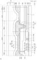
图1是根据本公开的实施例的电致发光显示装置的平面图;1 is a plan view of an electroluminescent display device according to an embodiment of the present disclosure;
图2是沿着根据本公开的实施例的图1的线I-I’截取的剖视图;2 is a cross-sectional view taken along line I-I' of FIG. 1 according to an embodiment of the present disclosure;
图3是根据本公开的实施例的图2的部分A的放大图;FIG. 3 is an enlarged view of part A of FIG. 2 according to an embodiment of the present disclosure;
图4A至图4D是示出根据本公开的实施例的电致发光显示装置的制造方法的图。4A to 4D are diagrams illustrating a method of manufacturing an electroluminescent display device according to an embodiment of the present disclosure.
具体实施方式Detailed ways
现在将详细参考本公开的实施例,实施例的示例在附图中示出。尽可能地,相同的附图标记将在所有附图中用于表示相同或相似的部件。Reference will now be made in detail to the embodiments of the present disclosure, examples of which are illustrated in the accompanying drawings. Wherever possible, the same reference numbers will be used throughout the drawings to refer to the same or like parts.
本公开的优点和特征以及其实现方法将通过以下结合附图描述的实施例来阐明。然而,本公开可以以不同的形式体现,并且不应被解释为限于在此阐述的实施例。反之,提供这些实施例是为了使本公开彻底和完整,并将本公开的范围充分传达给本领域技术人员。此外,本公开仅由权利要求的范围限定。The advantages and features of the present disclosure and methods for achieving the same will be clarified by the following embodiments described in conjunction with the accompanying drawings. The present disclosure may, however, be embodied in different forms and should not be construed as limited to the embodiments set forth herein. Rather, these embodiments are provided so that this disclosure will be thorough and complete, and will fully convey the scope of the disclosure to those skilled in the art. Furthermore, the present disclosure is to be limited only by the scope of the claims.
用于描述本公开的实施例的附图中公开的形状、尺寸、比率、角度和数量仅仅是示例,因此,本公开不限于图示细节。在整个说明书中,相似的附图标记表示相似的元件。在下面的描述中,当确定相关已知功能或配置的详细描述不必要地模糊本公开的要点时,将省略该详细描述。在使用本公开中描述的“包括”、“具有”和“包含”的情况下,可以添加另一部件,除非使用了“仅~”。单数形式的术语可以包括复数形式,除非提及相反的意思。The shapes, sizes, ratios, angles, and numbers disclosed in the drawings for describing embodiments of the present disclosure are merely examples, and thus, the present disclosure is not limited to the illustrated details. Throughout the specification, like reference numerals refer to like elements. In the following description, when it is determined that the detailed description of related known functions or configurations unnecessarily obscure the gist of the present disclosure, the detailed description will be omitted. Where "including", "having" and "comprising" described in this disclosure are used, another component may be added unless "only -" is used. Terms in the singular may include the plural unless the contrary is mentioned.
在解释一个元件时,尽管没有明确的描述,但该元件被解释为包含误差范围。When explaining an element, even though not explicitly described, the element is interpreted as containing a range of error.
在描述位置关系时,例如,当两个部分之间的位置关系被描述为“在~上”、“在~上方”、“在~下方”和“在~旁边”时,一个或多个部分可以设置在两个部分之间,除非使用了“仅”或“直接”。When describing a positional relationship, for example, when the positional relationship between two parts is described as "on ~ above", "above ~", "below ~" and "beside ~", one or more parts Can be set between two parts, unless "only" or "direct" is used.
在描述时间关系时,例如,当时间顺序被描述为“在~之后”、“随后~”、“接着~”和“在~之前”时,可以包括不连续的情况,除非使用了“仅”或“直接”。When describing a temporal relationship, for example, when the chronological sequence is described as "after ~", "subsequent to ~", "next to" and "before ~", discontinuities may be included unless "only" is used or "direct".
应理解,尽管术语“第一”、“第二”等可以在本文中用于描述各种元件,但这些元件不应受这些术语的限制。这些术语仅用于区分一个元件和另一个元件。例如,在不偏离本公开的范围的情况下,第一元件可以称为第二元件,并且类似地,第二元件可以称为第一元件。It will be understood that, although the terms "first," "second," etc. may be used herein to describe various elements, these elements should not be limited by these terms. These terms are only used to distinguish one element from another. For example, a first element could be termed a second element, and, similarly, a second element could be termed a first element, without departing from the scope of the present disclosure.
在描述本公开的元件时,可以使用诸如第一、第二、A、B、(a)、(b)等的术语。这些术语仅用于将相应元件与其他元件区分开,并且相应元件的本质、顺序或优先级不受这些术语的限制。应理解,当一个元件或层被称为在另一元件或层“上”或“连接到”另一元件或层时,它可以直接在另一元件或层上或直接连接到另一元件或层,或者可以存在中间元件或层。另外,应理解,当一个元件设置在另一元件上方或下方时,这可以表示元件被设置成彼此直接接触的情况,但也可以表示元件被设置成彼此不直接接触的情况。In describing elements of the present disclosure, terms such as first, second, A, B, (a), (b), etc. may be used. These terms are only used to distinguish the corresponding element from other elements, and the nature, order, or priority of the corresponding elements is not limited by these terms. It will be understood that when an element or layer is referred to as being "on" or "connected to" another element or layer, it can be directly on or directly connected to the other element or layer or layers, or intervening elements or layers may be present. Additionally, it should be understood that when one element is positioned above or below another element, this can mean that the elements are positioned in direct contact with each other, but it can also mean that the elements are positioned not in direct contact with each other.
术语“至少一个”应该被理解为包括一个或多个相关联的所列项的任意和所有组合。例如,“第一项、第二项和第三项中的至少一个”的含义表示从第一项、第二项和第三项中的两个以上项中提出的所有项以及第一项、第二项或第三项的组合。The term "at least one" should be understood to include any and all combinations of one or more of the associated listed items. For example, the meaning of "at least one of the first, second, and third items" means all items presented from two or more of the first, second, and third items, as well as the first, second, and third items. A combination of the second or third item.
本公开的各种实施例的特征可以部分地或整体地彼此耦合或组合,并且可以如本领域技术人员能够充分理解的那样不同地彼此交互操作和在技术上驱动。本公开的实施例可以彼此独立地执行,或者可以相互依赖地一起执行。Features of various embodiments of the present disclosure may be coupled or combined with each other in part or in whole, and may interoperate and technically drive with each other differently as those skilled in the art can fully appreciate. Embodiments of the present disclosure may be performed independently of each other, or may be performed together in dependence on each other.
在下文中,将参考附图详细描述本公开的实施例。Hereinafter, embodiments of the present disclosure will be described in detail with reference to the accompanying drawings.
图1是根据本公开的实施例的平面图。FIG. 1 is a plan view of an embodiment according to the present disclosure.
参考图1,根据本公开的实施例的电致发光显示装置可以包括发光显示面板1和面板驱动电路单元3。Referring to FIG. 1 , an electroluminescent display device according to an embodiment of the present disclosure may include a light-emitting display panel 1 and a panel
显示面板1可以包括基板10、有源区域AA、非有源区域、第一电源线60、第二电源线70和栅极驱动电路50。The display panel 1 may include a
基板10可以是玻璃基板、可弯曲的薄玻璃基板、塑料基板或硅晶片基板。The
有源区域AA是显示图像的区域,也可以表示为第一区域、显示部、显示区域或有源部。例如,有源区域AA可以设置在基板10的除边缘部分之外的部分中。The active area AA is an area where an image is displayed, and may also be represented as a first area, a display portion, a display area, or an active portion. For example, the active area AA may be provided in a portion of the
非有源区域IA是不显示图像的区域,也可以表示为第二区域、非显示部、非显示区域或非有源部。例如,非显示部可以设置在基板10的边缘部分处以围绕有源区域AA。The non-active area IA is an area where no image is displayed, and may also be represented as a second area, a non-display portion, a non-display area, or a non-active portion. For example, the non-display part may be disposed at the edge portion of the
有源区域AA可以包括多个子像素,并且可以包括形成在多个子像素之间的至少一部分中的阴极接触区域CCA。The active area AA may include a plurality of subpixels, and may include a cathode contact area CCA formed in at least a portion between the plurality of subpixels.
在图1中,有源区域AA的结构可以包括第一子像素区域SPA1、与第一子像素区域SPA1相邻的第二子像素区域SPA2以及位于第一子像素区域SPA1与第二子像素区域SPA2之间的阴极接触区域CCA。In FIG. 1 , the structure of the active area AA may include a first sub-pixel area SPA1, a second sub-pixel area SPA2 adjacent to the first sub-pixel area SPA1, and the first sub-pixel area SPA1 and the second sub-pixel area SPA1 Cathode contact area CCA between SPA2.
在此,阴极接触区域CCA可以被定义为包括其中阴极接触电极270(稍后描述)的侧表面的一部分被暴露以接触第一电源连接线62和发光器件200的阴极250的区域的特定区域。稍后将参考图2和图3描述阴极接触区域CCA的详细结构。Here, the cathode contact area CCA may be defined as a specific area including a region where a portion of the side surface of the cathode contact electrode 270 (described later) is exposed to contact the first power
另外,在图1中,阴极接触区域CCA被示出为相对于第一方向X位于第一子像素区域SPA1的一侧和第二子像素区域SPA2的一侧之间,但本公开的实施例不限于此。阴极接触区域CCA可以基于第一子像素区域SPA1应用于不同的位置,而没有任何特定的位置限制。例如,阴极接触区域CCA可以相对于第二方向Y位于第一子像素区域SPA1的一侧或另一侧。可替代地,阴极接触区域CCA可以被布置为面对第一子像素区域SPA1的边缘。In addition, in FIG. 1 , the cathode contact area CCA is shown as being located between one side of the first subpixel area SPA1 and one side of the second subpixel area SPA2 with respect to the first direction X, but embodiments of the present disclosure Not limited to this. The cathode contact area CCA may be applied to different positions based on the first sub-pixel area SPA1 without any specific position limitation. For example, the cathode contact area CCA may be located on one side or the other side of the first sub-pixel area SPA1 with respect to the second direction Y. Alternatively, the cathode contact area CCA may be arranged to face the edge of the first sub-pixel area SPA1.
根据本公开的实施例的电致发光显示装置可以包括设置在非有源区域IA中的第一电源线60和第二电源线70。在此,基极电压VSS和源极电压VDD可以分别施加到第一电源线60和第二电源线70。第一电源线60和第二电源线70可以由面板驱动电路单元3控制以分别向有源区域AA中的像素提供基极电压VSS和源极电压VDD。The electroluminescent display device according to an embodiment of the present disclosure may include a first
如图1所示,一对第一电源线60可以在显示面板1的顶部和底部以条形设置在非有源区域IA中,并且可以包括连接该对第一电源线60的多条第一电源连接线62。另外,一对第二电源线70可以在显示面板1的顶部和底部以条形设置在非有源区域IA中,并且可以包括连接该对第二电源线70的多条第二电源连接线72。As shown in FIG. 1 , a pair of
在图1中,第一电源连接线62可以设置成与阴极接触区域CCA的至少一部分重叠或者与阴极接触区域CCA相邻。在本公开中,阴极接触区域CCA可以通过提供第一电源连接线62可以与阴极(稍后描述)电接触的结构来提高可靠性,并且可以降低阴极的电阻。因此,可以提供具有改善的亮度均匀性的显示装置。In FIG. 1 , the first
栅极驱动电路50根据从驱动电路单元3提供的栅极控制信号通过焊盘部PP的多个栅极焊盘和连接线向栅极线提供栅极信号。例如,栅极驱动电路50可以设置在基板10的彼此面对的两侧的至少一个非有源区域IA中。栅极驱动电路50可以通过面板内栅极(GIP)方法形成在显示面板1的显示区域的一侧或两侧的非显示区域中。可替代地,栅极驱动器可以被制造为驱动芯片,安装在柔性层上方,并通过带式自动接合(TAB)方法附接到显示面板1的有源区域的一侧或两侧外面的非显示区域。The
根据一个示例的驱动电路单元3可以包括多个柔性电路膜31、多个数据驱动集成电路(IC)33、印刷电路板(PCB)35、时序控制器37和电源电路单元39。The driving
多个柔性电路膜31中的每一个可以附接到设置在基板10处的焊盘部PP和印刷电路板PCB 35。例如,多个柔性电路膜31中的每一个的一侧(或输出接合部)可以通过使用各向异性导电层的层附接工艺附接到设置在基板10处的焊盘部PP。多个柔性电路膜31中的每一个的另一侧(或输入接合部)可以通过使用各向异性导电层的层附接工艺附接到印刷电路板PCB 35。Each of the plurality of
多个数据驱动IC 33分别独立地安装在多个柔性电路膜31上方。多个数据驱动IC33中的每一个可以接收从时序控制器37提供的像素数据和数据控制信号,根据数据控制信号将像素数据转换为每个像素的模拟数据电压,并将数据电压提供给相应的数据线。The plurality of
印刷电路板PCB 35可以连接到多个柔性电路膜31中的每一个的另一侧。印刷电路板PCB 35可以用于在驱动电路单元3的部件之间传输信号和电压。The printed
时序控制器37可以安装在印刷电路板PCB 35上方并且通过设置在印刷电路板PCB35上方的连接器接收从显示驱动系统提供的图像数据和时序同步信号。The
时序控制器37可以基于时序同步信号通过将图像数据对准以适合设置在有源区域AA中的像素排列结构来产生像素数据,并将产生的像素数据提供给多个数据驱动IC 33中的每一个。The
时序控制器37可以基于时序同步信号产生数据控制信号和栅极控制信号,并通过数据控制信号控制多个数据驱动IC 33中的每一个的驱动时序。另外,时序控制器37可以通过栅极控制信号控制栅极驱动电路50的驱动时序。例如,时序同步信号可以包括垂直同步信号、水平同步信号、数据使能信号和主时钟(或点时钟)。The
电源电路单元39可以安装在印刷电路板PCB 35上方。另外,电源电路单元39可以使用从外部供应的输入电力产生在像素中显示图像所需的各种电源电压,并且可以将产生的电压提供给相应的电路。The
图2是沿着根据本公开的实施例的图1的线I-I’截取的剖视图,图3是根据本公开的实施例的图2的部分A的放大图。2 is a cross-sectional view taken along line I-I' of FIG. 1 according to an embodiment of the present disclosure, and FIG. 3 is an enlarged view of part A of FIG. 2 according to an embodiment of the present disclosure.
参考图2和图3,根据本公开的实施例的电致发光显示装置可以包括形成在基板110上方的驱动TFT T、平坦化层160、发光器件200、堤部180、阴极接触电极270和辅助电源线EVSS。Referring to FIGS. 2 and 3 , an electroluminescent display device according to an embodiment of the present disclosure may include a driving TFT T, a
在此,基板110可以具有与上面参考图1描述的基板10相同的配置。因此,基板110可以是玻璃基板、可弯曲的薄玻璃基板、塑料基板或硅基板。Here, the
驱动TFT T可以设置在缓冲层120中的有源区域AA中并且可以设置成对应于每个子像素。根据一个示例,驱动TFT T可以包括有源层ACT、栅极GE、源极SE和漏极DE。虽然驱动TFT T在图4中被示出为顶栅结构,但本公开的实施例不限于此,各种已知结构可以被应用于驱动TFT T。然而,在本公开中,将描述具有顶栅结构的驱动TFT。The driving TFT T may be disposed in the active area AA in the
缓冲层120可以设置在基板110和光阻挡层LS上方。根据一个示例,可以通过层叠多个无机层来形成缓冲层120。例如,缓冲层120可以形成为多层,其中层叠有一层或多层的氧化硅层(SiOx)、氮化硅层(SiN)和氮氧化硅层(SiON)的无机层。The
有源层ACT可以设置在缓冲层120上方。有源层ACT可以设置成与栅极GE、源极SE和漏极DE重叠,并且有源层ACT可以包括沟道区域和源极/漏极区域。有源层ACT的沟道区域可以形成为与栅极GE重叠,其中栅极绝缘层130插设在沟道区域与栅极GE之间。有源层ACT的源极/漏极区域可以彼此平行地形成,其中沟道区域插设在它们之间。另外,栅极绝缘层130可以设置在有源层ACT的沟道区域与栅极GE之间。栅极绝缘层130可以使有源层ACT和栅极GE绝缘。有源层ACT可以由硅基半导体材料或氧化物基半导体材料形成。The active layer ACT may be disposed over the
栅极绝缘层130可以设置在有源层ACT上方并且可以设置在缓冲层120上方。另外,栅极绝缘层130可以使有源层ACT和栅极GE绝缘。栅极绝缘层130可以形成为包括氮化硅层(SiNx)和氧化硅层(SiO2)中的至少一者的单层或多层。栅极绝缘层130的材料不限于此。The
栅极GE可以设置在栅极绝缘层130上方。栅极GE可以形成为由钼(Mo)、铝(Al)、铬(Cr)、金(Au)、银(Ag)、钛(Ti)、镍(Ni)、钕(Nd)、铜(Cu)、或前述金属的合金中的任一种形成的单层或多层。The gate GE may be disposed over the
层间绝缘层140可以设置在栅极GE和栅极绝缘层130上方。层间绝缘层140可用于保护驱动TFT T。层间绝缘层140的相应区域可以被去除以使有源层ACT与源极SE或漏极DE接触。例如,层间绝缘层140可以包括允许源极SE和有源层ACT的源极区域彼此接触的接触孔和允许漏极DE和有源层ACT的漏极区域彼此接触的接触孔。另外,层间绝缘层140可以形成在栅极绝缘层130上方。根据一个示例,层间绝缘层140可以包括氧化硅层(SiO2)或氮化硅层(SiN),或者可以包括包含氧化硅层(SiO2)和氮化硅层(SiN)的多个层。The interlayer insulating
根据本公开的实施例的源极SE和漏极DE可以形成为由钼(Mo)、铝(Al)、铬(Cr)、金(Au)、银(Ag)、钛(Ti)、镍(Ni)、钕(Nd)、铜(Cu)、或前述金属的合金中的任一种形成的单层或多层。在本公开中,可以使用满足驱动TFT T所需的特定电学特性的材料作为源极SE和漏极DE的所选材料。The source electrode SE and the drain electrode DE according to embodiments of the present disclosure may be formed of molybdenum (Mo), aluminum (Al), chromium (Cr), gold (Au), silver (Ag), titanium (Ti), nickel ( A single or multiple layers of Ni), neodymium (Nd), copper (Cu), or alloys of any of the foregoing metals. In the present disclosure, a material satisfying specific electrical characteristics required for driving the TFT T may be used as the selected material for the source electrode SE and the drain electrode DE.
另外,可以进一步包括设置在驱动TFT T的有源层ACT下方的光阻挡层LS。光阻挡层LS可以设置在基板110上方以与驱动TFT T重叠。例如,可以通过在基板110上方沉积金属层然后进行图案化来形成光阻挡层LS。光阻挡层LS可以是由诸如钼(Mo)、铝(Al)、铬(Cr)、金(Au)、银(Ag)、钛(Ti)、镍(Ni)、钕(Nd)和铜(Cu)的金属或前述金属的合金形成的单层或多层,但不限于此,并且可以用本领域已知的各种材料来实施。另外,光阻挡层LS可以包括下光阻挡层和上光阻挡层。In addition, a light blocking layer LS disposed under the active layer ACT of the driving TFT T may be further included. The light blocking layer LS may be disposed over the
保护层150可以设置在层间绝缘层140、源极SE和漏极DE上方。保护层150可以用于保护源极SE和漏极DE。保护层150可以包括允许像素电极210和源极SE彼此接触的接触孔。在此,保护层150的接触孔可以与平坦化层160的接触孔(其形成为允许像素电极210和源极SE彼此接触)重叠并连接。根据一个示例,保护层150可以是包括氧化硅层(SiO2)或氮化硅层(SiN)的单层。可替代地,保护层150可以包括包含氧化硅层(SiO2)和氮化硅层(SiN)的多个层。The
保护层150可以包括用于在阴极接触区域CCA或子像素区域SPA中阴极接触电极270和辅助电极AE的接触结构的第一接触孔CH1。第一接触孔CH1可以形成为与子像素区域SPA的非发光区域NEA的至少一部分重叠。在这种情况下,可以通过在厚度方向上去除整个保护层150来提供第一接触孔CH1。因此,可以通过形成在保护层150中的第一接触孔CH1提供阴极接触电极270和辅助电极AE的稳定的接触结构。The
平坦化层160可以设置在基板110上方以与包括第一子像素区域SPA1和第二子像素区域SPA2的子像素区域重叠。另外,平坦化层160可以形成为与阴极接触区域CCA重叠。具体地,平坦化层160可以与有源区域AA的发光区域EA重叠,使得由发光器件200和堤部180限定的发光区域EA形成为基本上平坦的。另外,平坦化层160可以与阴极接触区域CCA重叠。另外,如上所述,在平坦化层160中,由于用于辅助电极AE的接触结构的第一接触孔CH1形成在与阴极接触区域CCA相邻的非发光区域NEA中,平坦化层160可以被设置为使得其至少一部分在与阴极接触区域CCA相邻的非发光区域NEA中被去除。The
平坦化层160可以由诸如丙烯酸树脂、环氧树脂、酚醛树脂、聚酰胺树脂、聚酰亚胺树脂等的有机材料形成。The
发光器件200可以设置在平坦化层160上方并且可以电连接到驱动TFT T。发光器件200的像素电极210可以通过形成在平坦化层160和保护层150的至少一部分中的接触孔接触驱动TFT T的源极SE。The
根据本公开的实施例,发光器件200可以包括形成在平坦化层160上方并且形成在基板110中的有源区域AA的至少一部分中的像素电极210、形成为面对像素电极210并且形成为与整个有源区域AA重叠的阴极250以及形成在像素电极210与阴极250之间并且形成为对应于像素的发光层230。另外,根据制备相应层的方法,发光层230和阴极250可以形成为与邻近有源区域AA的非有源区域IA的至少一部分重叠,但不限于此。According to an embodiment of the present disclosure, the
像素电极210可以设置在平坦化层160上方并且可以电连接到驱动TFT T的源极SE。像素电极210可以通过设置在平坦化层160中的接触孔接触驱动TFT T的源极SE。The
像素电极210可以包括设置在平坦化层160上方的第一像素电极211和设置在第一像素电极211上方的第二像素电极213。The
第一像素电极211可以设置在平坦化层160上方,并且第二像素电极213可以设置成与第一像素电极211重叠。The
在这种情况下,第二像素电极213可以形成为具有与第一像素电极211基本相同的宽度。在包括第一像素电极211和第二像素电极213的像素电极210形成在平坦化层160上方之后,像素电极210可以被图案化以使用特定的掩模图案并执行蚀刻工艺来形成。In this case, the
在此,用于图案化像素电极210的蚀刻工艺可以是干蚀刻工艺。因此,如图2和图3所示,包括第一像素电极211和第二像素电极213的像素电极210可以通过干蚀刻工艺形成为在像素电极210的一侧和另一侧具有一定倾斜角,并且该倾斜角可以接近90度。因此,第一像素电极211和第二像素电极213可以形成为具有基本上相同的宽度。Here, the etching process for patterning the
包括第一像素电极211和第二像素电极213的像素电极210的一侧和另一侧可以被堤部180覆盖。One side and the other side of the
第一像素电极211和第二像素电极213中的每一个可以包括金属材料。Each of the
例如,第一像素电极211可以包括铜(Cu)、银(Ag)、钯(Pd)和铝(Al)中的至少一种,但不限于此。For example, the
例如,第二像素电极213可以包括氧化铟锡(ITO)、氧化铟锌(IZO)、钛(Ti)、钼(Mo)和钛钼(MoTi)合金中的至少一种,但不限于此。For example, the
另外,第一像素电极211可以包括与稍后描述的第一阴极接触电极271的材料相同的材料,并且第二像素电极213可以包括与稍后描述的第二阴极接触电极273的材料相同的材料。In addition, the
另外,根据本公开的实施例的像素电极210还可以包括分别设置在第一像素电极211下方和第二像素电极213上方的透明导电氧化物。因此,当包括透明导电氧化物时,根据本公开的实施例的像素电极210可以是具有四层结构的像素电极。In addition, the
堤部180可以限定每个子像素区域的发光区域EA。在每个子像素区域的发光区域EA中,像素电极210、发光层230和阴极250依次层叠以形成发光区域,来自像素电极210的空穴和来自阴极250的电子在该发光区域彼此结合以发光。在这种情况下,形成堤部180的区域不发光,因此成为非发光区域NEA,未形成堤部180并且暴露像素电极210的区域可成为发光区域EA。另外,堤部180可以形成为覆盖像素电极210的边缘并暴露像素电极210的一部分。因此,堤部180可以防止由于电流集中在像素电极210的端部而导致发光效率降低的问题。The
堤部180由诸如丙烯酸树脂、环氧树脂、酚醛树脂、聚酰胺树脂和聚酰亚胺树脂的有机材料形成。The
堤部180可以设置成覆盖阴极接触电极270(稍后将描述),并且可以形成为比阴极接触电极270的面对阴极接触区域CCA的一侧更突出。另外,在堤部180中,包括第一阴极接触电极271和第二阴极接触电极273的阴极接触电极270可以用作蚀刻工艺中的掩模图案以形成反向台阶结构。参考图2和图3,堤部180可以设置成与第一接触孔CH1重叠。因此,第一接触孔CH1可以被堤部填充或者堤部180可以填充在第一接触孔CH1内的空间中。The
另外,堤部180可以设置在多个像素电极210与阴极接触电极270之间以使彼此相邻的像素电极210和阴极接触电极270电绝缘。In addition, the
发光层230可以设置成与第一子像素区域SPA1中的发光区域EA的像素电极210的至少一部分重叠,并且可以设置成覆盖非发光区域NEA的堤部。另外,与第一子像素区域SPA1类似,发光层230可以设置成与第二子像素区域SPA2中的发光区域EA的像素电极210的至少一部分重叠,并且可以设置成覆盖非发光区域NEA的堤部,并且可以设置在平坦化层160上方以至少部分地与阴极接触区域CCA重叠。The
根据本公开的另一实施例,发光层230可以通过使用特定掩模图案在对应于每个子像素区域上进行沉积工艺来形成,并且当以这种方式形成时,发光层230可以形成为不与阴极接触区域CCA重叠。在本公开中,将基于不使用在有源区域AA中的单独的掩模图案而形成发光层230来描述发光层230。According to another embodiment of the present disclosure, the
如图2和图3所示,在与阴极接触区域CCA相邻的非发光区域NEA中,与第一子像素区域SPA1重叠的发光层230可以形成为具有厚度逐渐减小的尾巴形状。例如,发光层230的厚度可以具有非发光区域NEA在邻近阴极接触区域CCA的区域中变薄的尾巴形状。因此,设置在位于非发光区域NEA中的堤部上方的发光层230的厚度可以具有在邻近阴极接触区域CCA的部分中逐渐变薄的尾巴形状。与第二子像素区域SPA2重叠的发光层230’可以在与第二子像素区域SPA2相邻的一侧形成为平坦的,并且可以具有在朝向第一子像素区域SPA1的方向上厚度逐渐减小的尾巴形状。参考图2和图3,设置在第一子像素区域SPA1中的发光层230和设置在第二子像素区域SPA2中的发光层230’可以具有在底切(UC)区域中厚度逐渐减小的薄尾巴形状。As shown in FIGS. 2 and 3 , in the non-light emitting area NEA adjacent to the cathode contact area CCA, the
根据一个示例,发光层230可以包括空穴传输层、发光层和电子传输层。在这种情况下,当向像素电极210和阴极250施加电压时,空穴和电子分别通过空穴传输层和电子传输层移动到发光层,并在发光层中彼此结合以发光。根据一个示例,发光层230还可以包括至少一个功能层,以提高发光层230的发光效率和寿命。According to an example, the
阴极250可以设置在发光层230上方,并且阴极250可以以与有源区域AA共用的电极的形式来实现。在图2和图3中,第一子像素区域SPA1的阴极250和第二子像素区域SPA2的阴极250’被示出为物理断开,但这仅为图1的切割线I-I’的示例图。在未形成阴极接触区域CCA的有源区域AA中,多个子像素区域的阴极可以被设置成共同连接。The
因此,阴极250可以是共同地形成在子像素区域中以施加相同电压的公共层。阴极250可以由可以透射光的诸如ITO和IZO的透明导电材料(TCO)或诸如镁(Mg)、银(Ag)或镁(Mg)和银(Ag)的合金的半透射导电材料形成,但不限于此。Therefore, the
阴极250基于类似于发光层230的沉积工艺形成,但是由于无机层的性质,会具有比发光层230更高的台阶覆盖特性。另外,阴极250可以形成在有源区域AA中与有机发光层230重叠的所有区域中,并且还可以形成为与稍后描述的底切UC区域的至少一部分重叠。因此,第二子像素区域SPA2的阴极250’可以产生为与底切UC区域的至少一部分重叠并且可以与稍后描述的第一阴极接触电极271的一个侧表面接触。The
阴极接触电极270可以与阴极接触区域CCA相邻并且可以形成为与围绕发光区域EA的非发光区域NEA的至少一部分重叠。阴极接触电极270可以形成为与形成在保护层150和平坦化层160中的第一接触孔CH1的两个侧壁重叠。例如,阴极接触电极270的至少一部分可以沿着第一接触孔CH1的侧壁朝向平坦化层160的上表面延伸。另外,阴极接触电极270可以形成为至少部分地重叠在围绕第一接触孔CH1的平坦化层160的上表面上。另外,阴极接触电极270可以在平坦化层160上方延伸并突出到阴极接触区域CCA,以接触第二子像素区域SPA2的阴极250’。阴极250’可以与阴极接触电极270的侧表面接触。The
阴极接触电极270可以包括第一阴极接触电极271和第二阴极接触电极273。The
在这种情况下,第二阴极接触电极273可以设置在第一阴极接触电极271的上表面上方并且可以设置成与第一阴极接触电极271重叠。第一阴极接触电极271的至少一部分可以从接触孔CH1的形成在保护层150和平坦化层160中的区域侧壁朝向平坦化层160的上表面延伸,使得第一阴极接触电极271的侧表面设置在平坦化层160的上表面上。此外,尽管图2和图3示出了第一阴极接触电极271和第二阴极接触电极273形成为延伸到平坦化层160的上表面的示例,然而,应当理解,在其他实施例中,第一阴极接触电极271和第二阴极接触电极273形成为沿着第一接触孔CH1的侧壁延伸,使得第一阴极接触电极271或第二阴极接触电极273的侧表面设置在第一接触孔CH1的侧壁上。另外,第二阴极接触电极273的宽度可以大于第一阴极接触电极271的宽度,并且可以朝向例如阴极接触区域突出。因此,由于第一阴极接触电极271和第二阴极接触电极273,可以提供如下的反向台阶结构:在暴露阴极接触电极270的侧表面的区域中的侧表面处,位于第一阴极接触电极271上方的第二阴极接触电极273更突出。根据电致发光显示装置的设计,在暴露阴极接触电极270的侧表面的区域中,堤部180和阴极接触电极270进一步朝向阴极接触区域CCA延伸以至少部分地与阴极接触区域CCA重叠,或可以如图2所示与子像素区域的非发光区域NEA的至少一部分重叠。In this case, the second
如图3所示,第二阴极接触电极273可以被设置为相对于堤部180的朝向阴极接触区域CCA的端部以第一宽度W1朝向发光区域EA形成底切UC区域,并且第一阴极接触电极271可以被设置为相对于第二阴极接触电极273的朝向阴极接触区域CCA的端部以第二宽度W2朝向发光区域EA形成底切UC区域。As shown in FIG. 3 , the second
在这种情况下,第一宽度W1可以大于第二阴极接触电极273的厚度,第二宽度W2可以大于第一阴极接触电极271的厚度。因此,第一宽度W1和第二宽度W2之和可以大于第二阴极接触电极273的厚度和第一阴极接触电极271的厚度之和。In this case, the first width W1 may be greater than the thickness of the second
底切UC区域可以被限定为具有其中包括第一阴极接触电极271和第二阴极接触电极273的阴极接触电极270基于堤部180的朝向阴极接触区域CCA的端部被进一步向内侧蚀刻并且位于第二阴极接触电极273下方的第一阴极接触电极271的一侧形成在比第二阴极接触电极273的一侧的更靠内侧处。具体来说,堤部180的一部分可以突出到第一阴极接触电极271的侧表面之外。第二阴极接触电极273可以设置在第一阴极接触电极271上,使得第二阴极接触电极273的侧表面突出到第一阴极接触电极271的侧表面之外,并且第二阴极接触电极273的下表面暴露。堤部180也可以延伸到第二阴极接触电极273的侧表面之外以暴露堤部180的下表面。The undercut UC region may be defined as having the
因此,第一阴极接触电极271、第二阴极接触电极273和堤部180依次层叠在底切UC区域中的层叠结构可以具有多级反向台阶结构。另外,在图2和图3中,第一阴极接触电极271和第二阴极接触电极273以成角度的形式示出,但是具有第一阴极接触电极271和第二阴极接触电极273(其具有一定的粗糙度并且具有凹或凸的倾斜角)的轮廓的阴极接触电极270的结构也可以被认为包括在本公开的范围内。Therefore, the stacked structure in which the first
根据本公开的实施例,对于第一阴极接触电极271、第二阴极接触电极273和堤部180依次层叠在底切UC区域中的层叠结构,在形成多级反向台阶结构的蚀刻工艺中,当蚀刻工艺作为单个工艺执行时,第一阴极接触电极271的蚀刻工艺的蚀刻速率可以高于第二极接触电极273的蚀刻工艺的蚀刻速率。According to an embodiment of the present disclosure, for a stacked structure in which the first
可替代地,对于第一阴极接触电极271、第二阴极接触电极273和堤部180依次层叠在底切UC区域中的层叠结构,在形成多级反向台阶结构的蚀刻工艺中,当蚀刻工艺作为多个蚀刻工艺(例如,两个蚀刻工艺)执行时,第一阴极接触电极271和第二阴极接触电极273可以在第一蚀刻工艺中同时被蚀刻,并且如上所述,第一阴极接触电极271的蚀刻工艺的蚀刻速率可以大于第二阴极接触电极273的蚀刻工艺的蚀刻速率,并且在第二蚀刻工艺中第一阴极接触电极271可以以相对较高的蚀刻速率被蚀刻。Alternatively, for the stacked structure in which the first
因此,如稍后将参考图4A至图4D描述的,在使用堤部180作为掩模图案形成阴极接触电极270的暴露的侧表面的情况下,可以通过执行单个蚀刻工艺或多个蚀刻工艺来制备包括具有第一阴极接触电极271和第二阴极接触电极273的阴极接触电极270和堤部180的反向台阶结构。Therefore, as will be described later with reference to FIGS. 4A to 4D , in the case of forming the exposed side surface of the
参考图2和图3,设置在第二子像素区域SPA2中的阴极250’可以与阴极接触电极270的第一阴极接触电极271的一个侧表面接触并电连接。因此,阴极的至少一部分可以在堤部180下方的区域中(更具体地,在堤部180的突出部下方的区域中)与阴极接触电极270的侧表面接触。阴极可以包括至少设置在第一子像素区域SPA1中的第一阴极(例如,250)和至少设置在第二子像素区域SPA2和阴极接触区域中的第二阴极(例如,250’),并且第二阴极可以与第一阴极接触电极271的侧表面接触。在一个例子中,第一阴极可以与第二阴极物理的断开。在另一个例子中,第一阴极与第二阴极一体形成。另外,与第一阴极接触电极271的一个侧表面接触的阴极250’的上表面可以与第二阴极接触电极273的下表面间隔开。因此,与第一阴极接触电极272的一个侧表面接触的阴极250’的厚度可以小于第一阴极接触电极271的厚度。2 and 3 , the cathode 250' disposed in the second subpixel area SPA2 may be in contact with and electrically connected to one side surface of the first
例如,第一阴极接触电极271可以包括铜(Cu)、银(Ag)、钯(Pd)和铝(Al)中的至少一种,但不限于此。For example, the first
例如,第二阴极接触电极273可以包括氧化铟锡(ITO)、氧化铟锌(IZO)、钛(Ti)、钼(Mo)和钛钼(MoTi)合金中的至少一种,但不限于此。For example, the second
因此,阴极接触电极270可以包括与像素电极210相同的材料并且可以具有相同的层叠结构。具体地,第一阴极接触电极271可以包括与第一像素电极211相同的材料,第二阴极接触电极273可以包括与第二像素电极213相同的材料。Therefore, the
另外,根据本公开的实施例的阴极接触电极270可以被设置为在一侧与像素电极210间隔开,并且阴极接触电极270与像素电极210通过上述的堤部180彼此电绝缘。In addition, the
稍后将参考图4A至图4D描述根据本公开的实施例的在层叠有第一阴极接触电极271、第二阴极接触电极273和堤部180的结构中形成反向台阶结构的制造方法。A manufacturing method of forming a reverse step structure in a structure in which the first
暴露在阴极接触区域CCA中的第一阴极接触电极271的侧表面可以接触第二子像素区域SPA2的阴极250’。A side surface of the first
因此,在根据本公开的实施例的电致发光显示器中,在阴极接触区域CCA中,阴极接触电极270不与与阴极250和250’表面接触,但在位于第一子像素区域SPA1一侧的非发光区域NEA中与阴极接触电极270的暴露的一个侧表面进行表面接触。因此,在根据本公开的实施例的电致发光显示装置中,由于不需要阴极接触电极270在阴极接触区域CCA中与阴极250和250’表面接触,所以阴极接触区域CCA可以被设计为具有小面积,并在设计规则上有优势。在此,表面接触可以被定义为阴极接触电极270的上表面与阴极250和250’的下表面之间的接触。Therefore, in the electroluminescent display according to the embodiment of the present disclosure, in the cathode contact area CCA, the
辅助电极AE可以设置在层间绝缘层上方并且可以与稍后描述的辅助电源线EVSS接触。辅助电极AE可以通过上述的第一接触孔CH1接触阴极接触电极270。在此,阴极接触电极270与辅助电极AE之间可以通过形成在保护层150的与阴极接触区域CCA相邻的至少一部分中的接触孔CH1接触。The auxiliary electrode AE may be disposed over the interlayer insulating layer and may be in contact with the auxiliary power supply line EVSS described later. The auxiliary electrode AE may contact the
辅助电源线EVSS可以电连接到辅助电极AE并且可以包括与光阻挡层LS的材料相同的材料。辅助电源线EVSS可以设置在基板110上方。因此,辅助电源线EVSS可以由包括金属(例如,铜(Cu)、钛(Ti)、钼(Mo)、铝(Al)、铬(Cr)和银(Ag)或前述材料的合金)的单层或多层形成,但不限于此,并且可以用本领域已知的各种材料实现。The auxiliary power supply line EVSS may be electrically connected to the auxiliary electrode AE and may include the same material as that of the light blocking layer LS. The auxiliary power line EVSS may be disposed above the
以上参考图1描述的第一电源连接线62可以具有与辅助电源线EVSS和辅助电极AE相同的配置。在图1中,由于显示限制,第一电源连接线62被示出为单条线,但可以包括辅助电源线EVSS和辅助电极AE,并且可以改善阴极的电阻均匀性。The first power
辅助电极AE可以通过形成在层间绝缘层140的至少一部分中的第二接触孔CH2接触辅助电源线EVSS。在此,根据需要,可以通过去除缓冲层120和层间绝缘层140的至少一部分来形成第二接触孔CH2。The auxiliary electrode AE may contact the auxiliary power supply line EVSS through the second contact hole CH2 formed in at least a part of the interlayer insulating
辅助电极AE可以被设置为在层间绝缘层140上方与源极SE和漏极DE间隔开,并且可以由与源极SE和漏极DE相同的材料形成并且在相同的工艺中制备。辅助电极AE可以具有与源极SE和漏极DE相同的层叠结构。因此,辅助电极AE可以形成为包括钼(Mo)、铝(Al)、铬(Cr)、金(Au)、银(Ag)、钛(Ti)、镍(Ni))、钕(Nd)、铜(Cu)、或前述金属的合金的单层或多层。The auxiliary electrode AE may be disposed to be spaced apart from the source electrode SE and the drain electrode DE over the interlayer insulating
根据本公开的实施例,在发光区域EA中,平坦化层160可以包括接触孔,像素电极210穿过该接触孔。在此,平坦化层160的接触孔可以连接到保护层150的接触孔以允许像素电极210穿过。例如,平坦化层160可以包括诸如光丙烯酸和聚酰亚胺的有机材料。According to an embodiment of the present disclosure, in the light emitting area EA, the
封装部170可以覆盖子像素区域SPA1和SPA2以及阴极接触区域CCA,并且可以覆盖非有源区域IA的至少一部分。根据本公开的实施例,封装部170可以包括至少一个无机层和至少一个有机层。另外,封装部170可以具有无机层和有机层交替布置的薄膜封装结构,并且可以防止湿气或氧气渗透到发光器件200中。例如,封装部170可以包括依次层叠的第一封装部171、第二封装部172和第三封装部173。另外,封装部170的第一封装部171和第三封装部173可以是无机层,第二封装部172可以是有机层,但不限于此。The
另外,如图2和图3所示,第一封装部171可以被设置成覆盖第一子像素区域SPA1、第二子像素区域SPA2和阴极接触区域CCA。In addition, as shown in FIGS. 2 and 3 , the
根据本公开的实施例的电致发光显示装置可以设置为在与阴极接触区域CCA的至少一部分重叠的区域中包括平坦化层160的结构。另外,位于第一子像素区域SPA1的非发光区域NEA中的第一封装部171的上表面与位于阴极接触区域CCA中的第一封装部171的上表面之间的台阶高度d可以设置为在与堤部180和阴极接触电极270的厚度之和相同的高度处。因此,第一子像素区域SPA1的非发光部分NEA与阴极接触区域CCA之间的台阶高度d可以被减小或最小化,并且在形成第一封装部171的过程中,第一封装部171可以形成为覆盖第一子像素区域SPA1的非发光区域NEA和阴极接触区域CCA同时第一封装部171没有断开。The electroluminescent display device according to an embodiment of the present disclosure may be provided as a structure including the
第一封装部171和第三封装部173可以包括氧化硅层(SiOx)或氮化硅层(SiNx),但不限于此。第一封装部171和第三封装部173可以是包括氧化硅层(SiOx)和氮化硅层(SiNx)的多层。第二封装部172可以由有机材料形成,但不限于此。The
台阶高度d可以等于堤部和阴极接触电极的厚度之和。在这种情况下,阴极接触电极270的厚度可以被定义为形成在平坦化层160上方的第一阴极接触电极271和第二阴极接触电极273的厚度之和。另外,堤部180的厚度可以被定义为堤部180从平坦化层160上方的阴极接触电极270的上表面起的厚度。The step height d may be equal to the sum of the thicknesses of the bank and the cathode contact electrode. In this case, the thickness of the
在现有技术的电致发光显示装置中,在子像素区域的非发光部分和阴极接触区域中会形成大于或等于平坦化层的厚度的台阶高度,从而在形成第一封装部时由于未填充区域而可能会出现凹部或接缝,并且由这样的未填充区域引起的凹部或接缝可能充当湿气渗透路径或者可能由于结构不稳定而导致可靠性问题In the electroluminescent display device of the prior art, a step height greater than or equal to the thickness of the planarization layer is formed in the non-light-emitting portion of the sub-pixel region and the cathode contact region, so that when the first encapsulation portion is formed, the unfilled portion is not filled. Indentations or seams may occur due to such unfilled areas and may act as moisture penetration paths or may cause reliability issues due to structural instability
图4A至图4D依次示出了根据本公开的实施例的电致发光显示装置的制造方法的工艺。FIGS. 4A to 4D sequentially illustrate the processes of a method of manufacturing an electroluminescent display device according to an embodiment of the present disclosure.
参考图4A至图4D,可以通过沉积工艺制备包括第一像素电极211和第二像素电极213的像素电极210以及包括第一阴极接触电极271和第二阴极接触电极273的阴极接触电极270。4A to 4D , the
可以使用掩模图案使像素电极210和阴极接触电极270在预定区域中被图案化。在此,对于像素电极210而言,预定区域可以是对应于发光区域EA的区域,对于阴极接触电极270而言,预定区域可以是对应于与阴极接触区域CCA相邻的非发光区域NEA的区域。另外,第一阴极接触电极271和第二阴极接触电极273可以由与第一像素电极211和第二像素电极213相同的材料形成。因此,可以在单个工艺中形成像素电极210和阴极接触电极270。The
因此,此时,阴极接触电极270的一个侧表面和另一侧表面可以通过与像素电极210的一个侧表面和另一侧表面类似的法倾斜角(normal tapered angle)的蚀刻工艺形成为具有一定的倾斜度。Therefore, at this time, one side surface and the other side surface of the
接下来,形成用于分隔发光区域EA并使像素电极210和阴极接触电极270绝缘的堤部180。在这种情况下,堤部180可以设置为覆盖与像素电极210相邻的整个阴极接触电极270并且可以形成为暴露与阴极接触区域CCA相邻的阴极接触电极270或与阴极接触区域CCA的至少一部分重叠。Next, the
接下来,为了形成包括具有第一阴极接触电极271和第二阴极接触电极273的阴极接触电极270和堤部180的反向台阶结构,可以在除了阴极接触区域CCA之外的区域中形成特定掩模图案MP并且可以执行阴极接触电极270的蚀刻工艺。另外,堤部180还可以用作蚀刻阴极接触电极270的掩模。Next, in order to form a reverse step structure including the
可以使用对于图案化工艺中使用的蚀刻工艺具有不同蚀刻速率的材料形成阴极接触电极270,并且在这种情况下,当蚀刻工艺作为单个工艺执行时,可以将第一阴极接触电极271的蚀刻工艺的蚀刻速率设置为具有比第二阴极接触电极273的蚀刻工艺的蚀刻速率更高的值。在此,蚀刻工艺可以是湿蚀刻。因此,在湿蚀刻工艺中使用的蚀刻剂的蚀刻速率对于第一阴极接触电极271可以大于第二阴极接触电极273。在此,作为蚀刻剂,可以使用已知的用于金属蚀刻的湿蚀刻剂。另外,上述蚀刻工艺不限于湿蚀刻,当将第一阴极接触电极271在干蚀刻工艺中的蚀刻速率和第二阴极接触电极273的在干蚀刻工艺中的蚀刻速率设置为不同时,可以使用干蚀刻工艺。The
另外,根据本公开的另一实施例,为了形成包括具有第一阴极接触电极271和第二阴极接触电极273的阴极接触电极270和堤部180的反向台阶结构,如果蚀刻工艺通过多个工艺进行,例如通过两个蚀刻工艺进行,第一阴极接触电极271和第二阴极接触电极273可以在第一蚀刻工艺中同时被蚀刻,并且如上所述,第一阴极接触电极271的蚀刻工艺的蚀刻速率可以大于第二阴极接触电极273的蚀刻工艺的蚀刻速率,并且在第二蚀刻工艺中,第一阴极接触电极271可以以相对较高的蚀刻速率被蚀刻。因此,在包括第一阴极接触电极271和第二阴极接触电极273的阴极接触电极270的情况下,当使用前述蚀刻工艺时,可以使用单个工艺将第二阴极接触电极273设置为重叠以对应于第一阴极接触电极271,第二阴极接触电极273的宽度可以大于第一阴极接触电极271的宽度。In addition, according to another embodiment of the present disclosure, in order to form the reverse step structure including the
接下来,形成发光器件200的发光层230和阴极250。在这种情况下,第二子像素区域SPA2的阴极250’可以与邻近阴极接触区域CCA相邻的非发光区域NEA中的阴极接触电极270的一个侧表面接触,具体地,与第一阴极接触电极271的一个侧表面接触。Next, the
因此,如上所述,包括第一阴极接触电极271和第二阴极接触电极273的阴极接触电极270可以在侧表面被暴露的部分中具有反向台阶结构。另外,如图2和图3所示,形成在包括第一阴极接触电极271和第二阴极接触电极273的阴极接触电极270的一侧的反向台阶结构被堤部180覆盖,并且形成在包括第一阴极接触电极271和第二阴极接触电极273的阴极接触电极270的另一侧表面的反向台阶结构可以以暴露在阴极接触区域中的形式提供而不被堤部180覆盖。Therefore, as described above, the
在此,阴极接触电极270的暴露在阴极接触区域中的侧表面可以接触第二子像素区域SPA2的发光器件的阴极250’。Here, the side surface of the
根据本公开的实施例,具有在电致发光显示装置的整个有源区域上提供均匀的阴极电阻的效果。According to the embodiments of the present disclosure, there is an effect of providing uniform cathode resistance over the entire active area of the electroluminescent display device.
另外,根据本公开的实施例,具有在电致发光显示装置的阴极接触区域中阻挡湿气渗透的路径的效果。In addition, according to the embodiments of the present disclosure, there is an effect of blocking the path of moisture penetration in the cathode contact region of the electroluminescent display device.
本公开的效果不限于上述效果,本领域技术人员通过以下描述将清楚地理解本文未提及的其他效果。The effects of the present disclosure are not limited to the above-described effects, and other effects not mentioned herein will be clearly understood by those skilled in the art from the following description.
本公开的上述特征、结构和效果被包含在本公开的至少一个实施例中,但不仅限于一个实施例。此外,本领域技术人员可以通过其他实施例的组合或修改来实现本公开的至少一个实施例中描述的特征、结构和效果。因此,与所述组合和修改有关的内容应被理解为在本公开的范围内。The above-described features, structures, and effects of the present disclosure are included in at least one embodiment of the present disclosure, but are not limited to only one embodiment. Furthermore, those skilled in the art may realize the features, structures and effects described in at least one embodiment of the present disclosure by combining or modifying other embodiments. Accordingly, matters relating to the described combinations and modifications should be construed as being within the scope of the present disclosure.
显然,对本领域技术人员而言,在不偏离本公开的精神或范围的情况下,可以在本公开中进行各种修改和变化。因此,本公开旨在覆盖本公开的修改和变化,只要它们落入所附权利要求及其等同物的范围内。It will be apparent to those skilled in the art that various modifications and variations can be made in the present disclosure without departing from the spirit or scope of the disclosure. Therefore, this disclosure is intended to cover modifications and variations of this disclosure provided they come within the scope of the appended claims and their equivalents.
Claims (20)
Translated fromChineseApplications Claiming Priority (2)
| Application Number | Priority Date | Filing Date | Title |
|---|---|---|---|
| KR1020200169660AKR102817751B1 (en) | 2020-12-07 | 2020-12-07 | Electroluminescence display device |
| KR10-2020-0169660 | 2020-12-07 |
Publications (1)
| Publication Number | Publication Date |
|---|---|
| CN114597242Atrue CN114597242A (en) | 2022-06-07 |
Family
ID=81814135
Family Applications (1)
| Application Number | Title | Priority Date | Filing Date |
|---|---|---|---|
| CN202111485768.9APendingCN114597242A (en) | 2020-12-07 | 2021-12-07 | Electroluminescent display device |
Country Status (3)
| Country | Link |
|---|---|
| US (1) | US20220181399A1 (en) |
| KR (1) | KR102817751B1 (en) |
| CN (1) | CN114597242A (en) |
Families Citing this family (4)
| Publication number | Priority date | Publication date | Assignee | Title |
|---|---|---|---|---|
| US20230123636A1 (en)* | 2020-03-25 | 2023-04-20 | Sharp Kabushiki Kaisha | Display device and method of manufacturing display device |
| KR20230100004A (en)* | 2021-12-28 | 2023-07-05 | 엘지디스플레이 주식회사 | Display device |
| US20240276778A1 (en)* | 2022-04-26 | 2024-08-15 | Hefei Xinsheng Optoelectronics Technology Co., Ltd. | Display Substrate, Preparing Method Therefor, and Display Apparatus |
| US11882709B2 (en)* | 2022-05-12 | 2024-01-23 | Applied Materials, Inc. | High resolution advanced OLED sub-pixel circuit and patterning method |
Family Cites Families (22)
| Publication number | Priority date | Publication date | Assignee | Title |
|---|---|---|---|---|
| US9806279B2 (en)* | 2014-07-08 | 2017-10-31 | Lg Display Co., Ltd. | Organic light emitting display device comprising auxiliary electrode having void therein and manufacturing method thereof |
| US9570471B2 (en)* | 2014-08-05 | 2017-02-14 | Lg Display Co., Ltd. | Organic light emitting display device and method of manufacturing the same |
| CN106206656B (en)* | 2015-05-28 | 2019-11-15 | 乐金显示有限公司 | Organic light emitting display device and manufacturing method thereof |
| KR102515033B1 (en)* | 2015-05-29 | 2023-03-28 | 엘지디스플레이 주식회사 | Organic light emitting display device and method of manufacturing the same |
| KR102448611B1 (en)* | 2015-10-30 | 2022-09-27 | 엘지디스플레이 주식회사 | organic light emitting diode display |
| EP3240036B1 (en)* | 2016-04-29 | 2024-05-01 | LG Display Co., Ltd. | Organic light-emitting display device and method of manufacturing the same |
| KR101878187B1 (en)* | 2016-07-29 | 2018-07-13 | 엘지디스플레이 주식회사 | Organic light emitting display and fabricating method thereof |
| KR101878186B1 (en)* | 2016-07-29 | 2018-08-17 | 엘지디스플레이 주식회사 | Organic light emitting display and fabricating method thereof |
| KR102693312B1 (en)* | 2016-09-30 | 2024-08-07 | 엘지디스플레이 주식회사 | Organic light emitting display device and method of manufacturing the same |
| KR101980780B1 (en)* | 2016-10-31 | 2019-05-21 | 엘지디스플레이 주식회사 | Organic light emitting display device and method of manufacturing the same |
| JP6947536B2 (en)* | 2017-05-26 | 2021-10-13 | 株式会社ジャパンディスプレイ | Display device |
| KR102461391B1 (en)* | 2017-10-16 | 2022-10-31 | 엘지디스플레이 주식회사 | Large Area Organic Light Emitting Diode Display |
| KR102387343B1 (en)* | 2017-12-20 | 2022-04-15 | 엘지디스플레이 주식회사 | Display device |
| KR102482991B1 (en)* | 2017-12-28 | 2022-12-29 | 엘지디스플레이 주식회사 | Top Emission Type Organic Light Emitting Diode Display |
| KR102248402B1 (en)* | 2018-04-19 | 2021-05-04 | 엘지디스플레이 주식회사 | Electro-Luminescent Display Device and method of fabricating the same |
| KR102598834B1 (en)* | 2018-10-31 | 2023-11-06 | 엘지디스플레이 주식회사 | Display apparatus |
| KR102717811B1 (en)* | 2018-10-31 | 2024-10-15 | 엘지디스플레이 주식회사 | Organic Light Emitting Display Device |
| KR102819368B1 (en)* | 2018-11-19 | 2025-06-11 | 엘지디스플레이 주식회사 | Display device |
| KR102749163B1 (en)* | 2019-12-20 | 2025-01-03 | 엘지디스플레이 주식회사 | Display device and manufacturing method thereof |
| KR20210086162A (en)* | 2019-12-31 | 2021-07-08 | 엘지디스플레이 주식회사 | Organic light emitting display device |
| KR102795157B1 (en)* | 2020-06-24 | 2025-04-14 | 엘지디스플레이 주식회사 | Display Device |
| KR20220069361A (en)* | 2020-11-20 | 2022-05-27 | 엘지디스플레이 주식회사 | Light emitting display device |
- 2020
- 2020-12-07KRKR1020200169660Apatent/KR102817751B1/enactiveActive
- 2021
- 2021-12-06USUS17/543,522patent/US20220181399A1/enactivePending
- 2021-12-07CNCN202111485768.9Apatent/CN114597242A/enactivePending
Also Published As
| Publication number | Publication date |
|---|---|
| KR20220080492A (en) | 2022-06-14 |
| KR102817751B1 (en) | 2025-06-05 |
| US20220181399A1 (en) | 2022-06-09 |
Similar Documents
| Publication | Publication Date | Title |
|---|---|---|
| TWI648851B (en) | Display device | |
| CN109994517B (en) | Electroluminescence display device | |
| CN110010621B (en) | Electroluminescent display device | |
| CN114597242A (en) | Electroluminescent display device | |
| US11171194B2 (en) | Display apparatus | |
| US12101964B2 (en) | Electroluminescence display apparatus | |
| CN108877520A (en) | A kind of display device and preparation method thereof | |
| US20250024709A1 (en) | Display device | |
| US20250280685A1 (en) | Organic light emitting display device | |
| CN115942771A (en) | Light emitting display device | |
| KR102636629B1 (en) | Display device | |
| CN113130570B (en) | Display device and method for manufacturing the same | |
| US20240023385A1 (en) | Electroluminescence Display | |
| US20250221263A1 (en) | Display device | |
| US20250275401A1 (en) | Display apparatus | |
| KR20230168392A (en) | Top Emission Type Electroluminescence Display | |
| WO2024197852A1 (en) | Driving backplane, light-emitting substrate, display panel, and display apparatus | |
| KR20250076025A (en) | Light emitting element and display device comprising the same | |
| CN117222258A (en) | Display apparatus | |
| CN120417703A (en) | Display device | |
| CN120076542A (en) | Display device | |
| KR20220097188A (en) | Light Emitting Diodes Display Apparatus | |
| KR20220081071A (en) | Electroluminescence display device | |
| KR20210081784A (en) | Display pannel and manufacturing method thereof |
Legal Events
| Date | Code | Title | Description |
|---|---|---|---|
| PB01 | Publication | ||
| PB01 | Publication | ||
| SE01 | Entry into force of request for substantive examination | ||
| SE01 | Entry into force of request for substantive examination |