CN114595657A - Chip layout method and device and electronic equipment - Google Patents
Chip layout method and device and electronic equipmentDownload PDFInfo
- Publication number
- CN114595657A CN114595657ACN202210220746.8ACN202210220746ACN114595657ACN 114595657 ACN114595657 ACN 114595657ACN 202210220746 ACN202210220746 ACN 202210220746ACN 114595657 ACN114595657 ACN 114595657A
- Authority
- CN
- China
- Prior art keywords
- chip
- laid out
- file
- layout
- def file
- Prior art date
- Legal status (The legal status is an assumption and is not a legal conclusion. Google has not performed a legal analysis and makes no representation as to the accuracy of the status listed.)
- Pending
Links
Images


Classifications
- G—PHYSICS
- G06—COMPUTING OR CALCULATING; COUNTING
- G06F—ELECTRIC DIGITAL DATA PROCESSING
- G06F30/00—Computer-aided design [CAD]
- G06F30/30—Circuit design
- G06F30/39—Circuit design at the physical level
- G06F30/392—Floor-planning or layout, e.g. partitioning or placement
- G—PHYSICS
- G06—COMPUTING OR CALCULATING; COUNTING
- G06F—ELECTRIC DIGITAL DATA PROCESSING
- G06F30/00—Computer-aided design [CAD]
- G06F30/30—Circuit design
- G06F30/39—Circuit design at the physical level
- G06F30/398—Design verification or optimisation, e.g. using design rule check [DRC], layout versus schematics [LVS] or finite element methods [FEM]
Landscapes
- Engineering & Computer Science (AREA)
- Computer Hardware Design (AREA)
- Physics & Mathematics (AREA)
- Theoretical Computer Science (AREA)
- Evolutionary Computation (AREA)
- Geometry (AREA)
- General Engineering & Computer Science (AREA)
- General Physics & Mathematics (AREA)
- Architecture (AREA)
- Design And Manufacture Of Integrated Circuits (AREA)
Abstract
Description
Translated fromChinese技术领域technical field
本发明涉及集成电路设计技术领域,尤其涉及一种芯片布局方法、装置及电子设备。The present invention relates to the technical field of integrated circuit design, and in particular, to a chip layout method, device and electronic device.
背景技术Background technique
芯片设计进入深亚微米时代后,芯片布局(Floorplan)成为超大规模集成电路(Very Large Scale Integration,VLSI)的重要设计阶段。在布局(Floorplan)阶段,通过定义芯片或块的大小和形状,将IO引脚/焊盘、宏和块放置在核心或芯片区域,以便有效地找到它们之间的布线空间,而布线空间是直接影响拥塞(Congestion)、路由(Routingissue)、电压降(IR drop)、时序(Timing)等的因素。After the chip design entered the deep sub-micron era, the chip layout (Floorplan) became an important design stage of the Very Large Scale Integration (VLSI). In the floorplan stage, by defining the size and shape of the chip or block, IO pins/pads, macros and blocks are placed in the core or chip area in order to efficiently find the routing space between them, and the routing space is directly Factors that affect congestion (Congestion), routing (Routingissue), voltage drop (IR drop), timing (Timing), etc.
目前,多通过ICC2等传统电子设计自动化(Electronics Design Automation,EDA)工具展示芯片布局,但EDA工具在每次展示芯片布局时均需获取大量数据和文件,运行效率较低。At present, the chip layout is mostly displayed through traditional electronic design automation (Electronics Design Automation, EDA) tools such as ICC2, but the EDA tool needs to acquire a large amount of data and files every time the chip layout is displayed, and the operation efficiency is low.
发明内容SUMMARY OF THE INVENTION
本发明提供一种芯片布局方法、装置及电子设备,用以解决现有技术中EDA工具展示芯片布局运行效率较低的缺陷。The present invention provides a chip layout method, device, and electronic equipment, which are used to solve the defect of low operation efficiency of EDA tool display chip layout in the prior art.
本发明提供一种芯片布局方法,包括:The present invention provides a chip layout method, comprising:
解析待布局芯片的初始DEF文件,确定所述待布局芯片的属性信息,并通过视图组件显示所述属性信息,以使用户基于显示的属性信息确定布局指令;Parse the initial DEF file of the chip to be laid out, determine the attribute information of the chip to be laid out, and display the attribute information through the view component, so that the user can determine the layout instruction based on the displayed attribute information;
在检测到所述布局指令的情况下,基于所述布局指令调整所述待布局芯片的位置,并基于所述待布局芯片调整后的位置信息更新所述初始DEF文件或生成新DEF文件。When the layout instruction is detected, the position of the chip to be laid out is adjusted based on the layout instruction, and the initial DEF file is updated or a new DEF file is generated based on the adjusted position information of the chip to be laid out.
根据本发明提供的一种芯片布局方法,所述解析待布局芯片的初始DEF文件,之前还包括:According to a chip layout method provided by the present invention, the parsing of the initial DEF file of the chip to be laid out further includes:
基于所述待布局芯片的配置文件原始路径,确定所述待布局芯片的配置文件;determining the configuration file of the chip to be laid out based on the original path of the configuration file of the chip to be laid out;
打开所述配置文件,获取所述初始DEF文件。Open the configuration file to obtain the initial DEF file.
根据本发明提供的一种芯片布局方法,所述打开所述配置文件,之后还包括:According to a chip layout method provided by the present invention, the opening of the configuration file further includes:
解析所述待布局芯片的馈通文件,确定所述待布局芯片的馈通信息,并通过所述视图组件显示所述馈通信息。Parse the feedthrough file of the chip to be laid out, determine the feedthrough information of the chip to be laid out, and display the feedthrough information through the view component.
根据本发明提供的一种芯片布局方法,所述基于所述待布局芯片调整后的位置信息更新所述初始DEF文件或生成新DEF文件,之后还包括:保存所述待布局芯片的缓存文件。According to a chip layout method provided by the present invention, the step of updating the initial DEF file or generating a new DEF file based on the adjusted position information of the chip to be laid out further includes: saving a cache file of the chip to be laid out.
根据本发明提供的一种芯片布局方法,所述基于所述布局指令调整所述待布局芯片的位置,包括:According to a chip layout method provided by the present invention, the adjusting the position of the chip to be laid out based on the layout instruction includes:
基于所述布局指令,确定调整动作,并调用所述调整动作对应的工具栏调整所述待布局芯片的位置。Based on the layout instruction, an adjustment action is determined, and a toolbar corresponding to the adjustment action is invoked to adjust the position of the chip to be laid out.
根据本发明提供的一种芯片布局方法,所述基于所述布局指令调整所述待布局芯片的位置,之后还包括:According to a chip layout method provided by the present invention, the adjusting the position of the chip to be laid out based on the layout instruction further includes:
在检测到撤销操作指令的情况下,将所述待布局芯片的位置恢复至所述撤销操作指令中的目标位置。In the case that the undo operation instruction is detected, the position of the chip to be laid out is restored to the target position in the undo operation instruction.
根据本发明提供的一种芯片布局方法,所述解析待布局芯片的初始DEF文件,之前还包括:According to a chip layout method provided by the present invention, the parsing of the initial DEF file of the chip to be laid out further includes:
基于自定义标签,展示所述自定义标签对应的数据结构。Based on the custom label, the data structure corresponding to the custom label is displayed.
根据本发明提供的一种芯片布局方法,所述解析待布局芯片的初始DEF文件,之后还包括:According to a chip layout method provided by the present invention, the parsing of the initial DEF file of the chip to be laid out further includes:
获取并展示全芯片的时序路径信息。Obtain and display the timing path information of the whole chip.
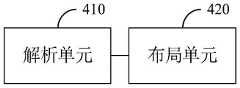
本发明还提供一种芯片布局装置,包括:The present invention also provides a chip layout device, comprising:
解析单元,用于解析待布局芯片的初始DEF文件,确定所述待布局芯片的属性信息,并通过视图组件显示所述属性信息,以使用户基于显示的属性信息确定布局指令;a parsing unit, configured to parse the initial DEF file of the chip to be laid out, determine the attribute information of the chip to be laid out, and display the attribute information through the view component, so that the user can determine the layout instruction based on the displayed attribute information;
布局单元,用于在检测到所述布局指令的情况下,基于所述布局指令调整所述待布局芯片的位置,并基于所述待布局芯片调整后的位置信息更新所述初始DEF文件或生成新DEF文件。A layout unit, configured to adjust the position of the chip to be laid out based on the layout instruction when the layout instruction is detected, and update the initial DEF file or generate the initial DEF file based on the adjusted position information of the chip to be laid out New DEF file.
本发明还提供一种电子设备,包括存储器、处理器及存储在存储器上并可在处理器上运行的计算机程序,所述处理器执行所述程序时实现如上述任一种所述芯片布局方法。The present invention also provides an electronic device, comprising a memory, a processor and a computer program stored in the memory and running on the processor, the processor implements any one of the chip layout methods described above when the processor executes the program .
本发明还提供一种非暂态计算机可读存储介质,其上存储有计算机程序,该计算机程序被处理器执行时实现如上述任一种所述芯片布局方法。The present invention also provides a non-transitory computer-readable storage medium on which a computer program is stored, and when the computer program is executed by a processor, implements any one of the above-mentioned chip layout methods.
本发明还提供一种计算机程序产品,包括计算机程序,所述计算机程序被处理器执行时实现如上述任一种所述芯片布局方法。The present invention also provides a computer program product, including a computer program, which implements any one of the above-mentioned chip layout methods when the computer program is executed by a processor.
本发明提供的芯片布局方法、装置及电子设备,通过解析待布局芯片的初始DEF文件即可显示待布局芯片的属性信息,而不需要像传统方法中需要获取大量文件后才能显示芯片布局,也就是本发明通过初始DEF文件即可显示待布局芯片的属性信息,大幅度提高了运行效率。此外,本发明基于待布局芯片调整后的位置信息更新初始DEF文件或生成新DEF文件,以便下次可以直接读取更新的初始DEF文件或新DEF文件,从而可以快速在视图组件中显示调整位置后的待布局芯片信息,而不需要重新加载大量文件获取调整位置后的待布局芯片信息,加快了FCFP的迭代速度。The chip layout method, device and electronic device provided by the present invention can display the attribute information of the chip to be laid out by parsing the initial DEF file of the chip to be laid out, and it is not necessary to obtain a large number of files before displaying the chip layout as in the traditional method. That is, the present invention can display the attribute information of the chip to be laid out through the initial DEF file, which greatly improves the operation efficiency. In addition, the present invention updates the initial DEF file or generates a new DEF file based on the adjusted position information of the chip to be laid out, so that the updated initial DEF file or the new DEF file can be directly read next time, so that the adjusted position can be quickly displayed in the view component After the information of the chip to be laid out after being placed, it is not necessary to reload a large number of files to obtain the information of the chip to be laid out after adjusting the position, which speeds up the iteration speed of FCFP.
附图说明Description of drawings
为了更清楚地说明本发明或现有技术中的技术方案,下面将对实施例或现有技术描述中所需要使用的附图作一简单地介绍,显而易见地,下面描述中的附图是本发明的一些实施例,对于本领域普通技术人员来讲,在不付出创造性劳动的前提下,还可以根据这些附图获得其他的附图。In order to explain the present invention or the technical solutions in the prior art more clearly, the following will briefly introduce the accompanying drawings that need to be used in the description of the embodiments or the prior art. Obviously, the accompanying drawings in the following description are the For some embodiments of the invention, for those of ordinary skill in the art, other drawings can also be obtained according to these drawings without any creative effort.
图1是本发明提供的芯片布局方法的流程示意图;1 is a schematic flowchart of a chip layout method provided by the present invention;
图2是本发明提供的加载恢复机制的流程示意图;2 is a schematic flow chart of a loading recovery mechanism provided by the present invention;
图3是本发明提供的视图组件界面示意图;3 is a schematic diagram of a view component interface provided by the present invention;
图4是本发明提供的芯片布局方法装置的结构示意图;4 is a schematic structural diagram of a chip layout method device provided by the present invention;
图5是本发明提供的电子设备的结构示意图。FIG. 5 is a schematic structural diagram of an electronic device provided by the present invention.
具体实施方式Detailed ways
为使本发明的目的、技术方案和优点更加清楚,下面将结合本发明中的附图,对本发明中的技术方案进行清楚、完整地描述,显然,所描述的实施例是本发明一部分实施例,而不是全部的实施例。基于本发明中的实施例,本领域普通技术人员在没有作出创造性劳动前提下所获得的所有其他实施例,都属于本发明保护的范围。In order to make the objectives, technical solutions and advantages of the present invention clearer, the technical solutions in the present invention will be clearly and completely described below with reference to the accompanying drawings. Obviously, the described embodiments are part of the embodiments of the present invention. , not all examples. Based on the embodiments of the present invention, all other embodiments obtained by those of ordinary skill in the art without creative efforts shall fall within the protection scope of the present invention.
目前,多通过ICC2等传统EDA工具展示芯片布局,但EDA工具在每次展示芯片布局时均需获取大量数据和文件,如请求整个数据库,获取网表(netlist文件)、芯片的DEF文件、lib库文件等,请求数据量较大导致运行效率较低。此外,EDA工具需要获取到上述所有文件后才能展示芯片布局,若缺少任一文件,则EDA工具无法展示芯片布局。At present, the chip layout is mostly displayed through traditional EDA tools such as ICC2, but the EDA tool needs to obtain a large amount of data and files each time the chip layout is displayed, such as requesting the entire database, obtaining the netlist (netlist file), the chip's DEF file, lib Library files, etc., the large amount of requested data leads to low operating efficiency. In addition, the EDA tool needs to obtain all the above files before displaying the chip layout. If any file is missing, the EDA tool cannot display the chip layout.
对此,本发明提供一种芯片布局方法。图1是本发明提供的芯片布局方法的流程示意图,如图1所示,该方法包括如下步骤:In this regard, the present invention provides a chip layout method. FIG. 1 is a schematic flowchart of a chip layout method provided by the present invention. As shown in FIG. 1 , the method includes the following steps:
步骤110、解析待布局芯片的初始DEF文件,确定待布局芯片的属性信息,并通过视图组件显示属性信息,以使用户基于显示的属性信息确定布局指令。Step 110: Parse the initial DEF file of the chip to be laid out, determine attribute information of the chip to be laid out, and display the attribute information through the view component, so that the user can determine the layout instruction based on the displayed attribute information.
此处,待布局芯片即需要进行布局的芯片。在首次对待布局芯片进行布局时,可以读取待布局芯片的初始DEF文件,并解析确定待布局芯片的属性信息。其中,待布局芯片的属性信息可以包括待布局芯片的大小、位置、方向等。Here, the chip to be laid out is the chip that needs to be laid out. When the chip to be laid out is laid out for the first time, the initial DEF file of the chip to be laid out can be read, and the attribute information of the chip to be laid out can be parsed and determined. The attribute information of the chip to be laid out may include the size, position, and direction of the chip to be laid out.
在获取待布局芯片的属性信息后,通过视图组件显示待布局芯片的属性信息,从而用户可以直观获取属性信息,并根据属性信息确定是否对待布局芯片的位置进行调整,如用户可以在视图组件窗口选择工具栏中的移动工具,对待布局芯片进行移动,其中,用户通过移动工具对待布局芯片进行移动可以看作是用户的布局指令。可选地,视图组件可以是基于QGraphicsView创建得到的。After obtaining the attribute information of the chip to be laid out, the attribute information of the chip to be laid out is displayed through the view component, so that the user can intuitively obtain the attribute information, and determine whether to adjust the position of the chip to be laid out according to the attribute information. Select the moving tool in the toolbar to move the chip to be laid out, wherein the user's movement of the chip to be laid out through the moving tool can be regarded as a layout instruction of the user. Optionally, the view component can be created based on QGraphicsView.
需要说明的是,本发明实施例中通过解析待布局芯片的初始DEF文件即可显示待布局芯片的属性信息,而不需要像传统方法中需要获取大量文件后才能显示芯片布局,也就是本发明实施例通过初始DEF文件即可显示待布局芯片的属性信息,大幅度提高了运行效率。此外,本发明实施例通过视图组件直观显示待布局芯片的属性信息,从而能够使用户直观获取待布局芯片的属性信息,进而便于沟通以及快速确定布局指令。再有,本发明实施例通过解析待布局芯片的DEF文件,可以单独显示待布局芯片的属性信息,并通过视图组件窗口单独对待布局芯片的位置进行调整,而不需要像传统方法中需要获取所有芯片的所有文件后才能展示芯片布局。可以理解的是,在需要同时显示多个待布局芯片的属性信息时,可以获取多个待布局芯片对应的初始DEF文件,进而可以在视图组件窗口同时显示多个待布局芯片的属性信息。It should be noted that, in the embodiment of the present invention, the attribute information of the chip to be laid out can be displayed by parsing the initial DEF file of the chip to be laid out, and it is not necessary to obtain a large number of files before displaying the chip layout as in the traditional method, which is the present invention. In the embodiment, the attribute information of the chip to be laid out can be displayed through the initial DEF file, which greatly improves the operation efficiency. In addition, in the embodiment of the present invention, the attribute information of the chip to be laid out is visually displayed through the view component, so that the user can intuitively obtain the attribute information of the chip to be laid out, thereby facilitating communication and quickly determining the layout instruction. Furthermore, in the embodiment of the present invention, by analyzing the DEF file of the chip to be laid out, the attribute information of the chip to be laid out can be displayed separately, and the position of the chip to be laid out can be adjusted independently through the view component window, without the need to obtain all the information in the traditional method. The chip layout can only be displayed after all the files for the chip. It can be understood that when the attribute information of multiple chips to be laid out needs to be displayed at the same time, the initial DEF files corresponding to the multiple chips to be laid out can be obtained, and then the attribute information of multiple chips to be laid out can be displayed simultaneously in the view component window.
步骤120、在检测到布局指令的情况下,基于布局指令调整待布局芯片的位置,并基于待布局芯片调整后的位置信息更新初始DEF文件或生成新DEF文件。Step 120 , when the layout instruction is detected, adjust the position of the chip to be laid out based on the layout instruction, and update the initial DEF file or generate a new DEF file based on the adjusted position information of the chip to be laid out.
具体地,布局指令中携带有调整动作,如移动待布局芯片、放大待布局芯片、缩小待布局芯片等。在用户基于视图组件所显示的属性信息确定布局指令后,基于布局指令中携带的调整动作,调整待布局芯片的位置,即实现可视化调整待布局芯片,并基于待布局芯片调整后的位置信息更新初始DEF文件或生成新DEF文件。Specifically, the layout instruction carries adjustment actions, such as moving the chip to be laid out, enlarging the chip to be laid out, shrinking the chip to be laid out, and the like. After the user determines the layout instruction based on the attribute information displayed by the view component, adjusts the position of the chip to be laid out based on the adjustment action carried in the layout instruction, that is, realizes visual adjustment of the chip to be laid out, and updates based on the adjusted position information of the chip to be laid out Initial DEF file or generate new DEF file.
在更新初始DEF文件或生成新DEF文件后,下次可以直接读取更新的初始DEF文件或新DEF文件,从而可以快速在视图组件中显示调整位置后的待布局芯片信息,而不需要重新加载大量文件获取调整位置后的待布局芯片信息,加快了FCFP的迭代速度。After updating the initial DEF file or generating a new DEF file, the updated initial DEF file or the new DEF file can be directly read next time, so that the position-adjusted chip information to be laid out can be quickly displayed in the view component without reloading A large number of files obtain the information of the chips to be laid out after adjusting the position, which speeds up the iteration speed of FCFP.
本发明实施例提供的芯片布局方法,通过解析待布局芯片的初始DEF文件即可显示待布局芯片的属性信息,而不需要像传统方法中需要获取大量文件后才能显示芯片布局,也就是本发明实施例通过初始DEF文件即可显示待布局芯片的属性信息,大幅度提高了运行效率。此外,本发明实施例基于待布局芯片调整后的位置信息更新初始DEF文件或生成新DEF文件,以便下次可以直接读取更新的初始DEF文件或新DEF文件,从而可以快速在视图组件中显示调整位置后的待布局芯片信息,而不需要重新加载大量文件获取调整位置后的待布局芯片信息,加快了FCFP的迭代速度。The chip layout method provided by the embodiment of the present invention can display the attribute information of the chip to be laid out by parsing the initial DEF file of the chip to be laid out, and does not need to acquire a large number of files before displaying the chip layout as in the traditional method, that is, the present invention In the embodiment, the attribute information of the chip to be laid out can be displayed through the initial DEF file, which greatly improves the operation efficiency. In addition, the embodiment of the present invention updates the initial DEF file or generates a new DEF file based on the adjusted position information of the chip to be laid out, so that the updated initial DEF file or the new DEF file can be directly read next time, so that it can be quickly displayed in the view component The information of the chip to be laid out after the position is adjusted, without reloading a large number of files to obtain the information of the chip to be laid out after the position adjustment, which speeds up the iteration speed of FCFP.
基于上述实施例,解析待布局芯片的初始DEF文件,之前还包括:Based on the above embodiment, the initial DEF file of the chip to be laid out is parsed, which also includes:
基于待布局芯片的配置文件原始路径,确定待布局芯片的配置文件;Determine the configuration file of the chip to be laid out based on the original path of the configuration file of the chip to be laid out;
打开配置文件,获取初始DEF文件。Open the configuration file to get the initial DEF file.
具体地,在首次对待布局芯片进行布局时,根据待布局芯片的配置文件原始路径,获取待布局芯片的配置文件,并打开配置文件,获取初始DEF文件。Specifically, when the chip to be laid out is laid out for the first time, the configuration file of the chip to be laid out is obtained according to the original path of the configuration file of the chip to be laid out, and the configuration file is opened to obtain the initial DEF file.
如图2所示,根据待布局芯片的配置文件原始路径,确定待布局芯片的配置文件(Config),进而可以获取待布局芯片的def文件(chip.def)、静态存储列表(sramlist)、馈通文件(Feedthrough)等。As shown in Figure 2, according to the original path of the configuration file of the chip to be laid out, the configuration file (Config) of the chip to be laid out is determined, and then the def file (chip. Feedthrough, etc.
基于上述任一实施例,打开配置文件,之后还包括:Based on any of the above embodiments, open the configuration file, and then further include:
解析待布局芯片的馈通文件,确定待布局芯片的馈通信息,并通过视图组件显示馈通信息。Parse the feedthrough file of the chip to be laid out, determine the feedthrough information of the chip to be laid out, and display the feedthrough information through the view component.
具体地,待布局芯片的配置文件中包含待布局芯片的馈通文件,因此在打开配置文件后,可以获取待布局芯片的馈通文件。通过解析馈通文件,可以确定待布局芯片的馈通信息,并通过视图组件显示馈通信息。其中,馈通信息可以包括总线数量,用于表征待布局芯片与其它芯片之间的拥塞情况,从而用户可以根据显示的馈通信息对待布局芯片的位置进行优化调整。Specifically, the configuration file of the chip to be laid out includes the feedthrough file of the chip to be laid out. Therefore, after the configuration file is opened, the feedthrough file of the chip to be laid out can be obtained. By parsing the feedthrough file, the feedthrough information of the chip to be laid out can be determined, and the feedthrough information can be displayed through the view component. The feedthrough information may include the number of buses to represent the congestion between the chip to be laid out and other chips, so that the user can optimize and adjust the position of the chip to be laid out according to the displayed feedthrough information.
例如,可以通过解析馈通文件(Feedthrough),将馈通信息以列表形式显示,并在视图组件的窗口中自定义选择需要显示的馈通信息。For example, the feedthrough information can be displayed in the form of a list by parsing the feedthrough file (Feedthrough), and the feedthrough information to be displayed can be customized and selected in the window of the view component.
基于上述任一实施例,基于待布局芯片调整后的位置信息更新初始DEF文件或生成新DEF文件,之后还包括:保存待布局芯片的缓存文件。Based on any of the foregoing embodiments, the initial DEF file is updated or a new DEF file is generated based on the adjusted position information of the chip to be laid out, and then the method further includes: saving a cache file of the chip to be laid out.
具体地,在基于待布局芯片调整后的位置信息更新初始DEF文件或生成新DEF文件之后,保存待布局芯片的缓存文件,从而在下次需要获取待布局芯片的最新布局信息时,可以通过直接打开缓存文件,进而能够加快获取待布局芯片的最新布局信息的速度。Specifically, after updating the initial DEF file or generating a new DEF file based on the adjusted position information of the chip to be laid out, the cache file of the chip to be laid out is saved, so that when the latest layout information of the chip to be laid out needs to be acquired next time, it can be directly opened Cache files, thereby speeding up the acquisition of the latest layout information of the chips to be laid out.
如图2所示,在基于待布局芯片调整后的位置信息更新初始DEF文件或生成新DEF文件后,可以保存待布局芯片的缓存文件(Chip.cache),从而下次可以直接打开该缓存文件获取待布局芯片调整位置后的信息,而不需要再重新获取大量文件,加速了FCFP的迭代速度。As shown in Figure 2, after updating the initial DEF file or generating a new DEF file based on the adjusted position information of the chip to be laid out, the cache file (Chip.cache) of the chip to be laid out can be saved, so that the cache file can be directly opened next time Obtain the information of the chip to be laid out after adjusting the position, without re-acquiring a large number of files, which speeds up the iteration speed of FCFP.
基于上述任一实施例,基于布局指令调整待布局芯片的位置,包括:Based on any of the foregoing embodiments, adjusting the position of the chip to be laid out based on the layout instruction includes:
基于布局指令,确定调整动作,并调用调整动作对应的工具栏调整待布局芯片的位置。Based on the layout instruction, the adjustment action is determined, and the toolbar corresponding to the adjustment action is called to adjust the position of the chip to be laid out.
具体地,布局指令中携带有调整动作,如移动待布局芯片、放大待布局芯片、缩小待布局芯片等。在确定布局指令中的调整动作后,调用调整动作对应的工具栏调整待布局芯片的位置,从而可以快速完成对待布局芯片的调整。其中,工具栏中可以包括选择、标尺、移动、放大、缩小、重做、撤销等模式,以满足对待布局芯片进行布局时的多样化需求。Specifically, the layout instruction carries adjustment actions, such as moving the chip to be laid out, enlarging the chip to be laid out, shrinking the chip to be laid out, and the like. After the adjustment action in the layout instruction is determined, the toolbar corresponding to the adjustment action is called to adjust the position of the chip to be laid out, so that the adjustment of the chip to be laid out can be quickly completed. Among them, the toolbar may include modes such as selection, ruler, move, zoom in, zoom out, redo, and undo, so as to meet the diverse needs when laying out chips to be laid out.
如图3所示,视图组件显示界面由菜单栏(Menu Bar)、状态栏(Status Bar)、工具栏(Tool Bar)、浮动窗口(Dock Widget)和标签页(Tab Widget)组成。菜单栏主要包括打开(Open)、保存(Save)等功能,状态栏主要包括硬核(Hardmacro)、模块例化名(Instname)、坐标(Coordinate)等信息。工具栏主要包括一些常用的动作,比如选择(Select)、标尺(Ruler)、移动(Move)等。As shown in Figure 3, the view component display interface consists of a menu bar (Menu Bar), a status bar (Status Bar), a toolbar (Tool Bar), a floating window (Dock Widget) and a tab page (Tab Widget). The menu bar mainly includes functions such as Open and Save, and the status bar mainly includes information such as Hardmacro, Instname, and Coordinate. The toolbar mainly includes some commonly used actions, such as select (Select), ruler (Ruler), move (Move) and so on.
基于上述任一实施例,基于布局指令调整待布局芯片的位置,之后还包括:Based on any of the above embodiments, adjusting the position of the chip to be laid out based on the layout instruction, and then further comprising:
在检测到撤销操作指令的情况下,将待布局芯片的位置恢复至撤销操作指令中的目标位置。When the undo operation instruction is detected, the position of the chip to be laid out is restored to the target position in the undo operation instruction.
具体地,在用户需要撤销对待布局芯片的调整时,可以在工具栏中选取撤销模式,以生成撤销操作指令,将待布局芯片的位置恢复至撤销操作指令中的目标位置。其中,在选取撤销模式后,可以从对应的撤销列表中选择任意位置作为目标位置,以将待布局芯片的位置快速恢复至撤销操作指令中的目标位置。Specifically, when the user needs to undo the adjustment of the chip to be laid out, the undo mode can be selected in the toolbar to generate an undo operation instruction and restore the position of the chip to be laid out to the target position in the undo operation instruction. Wherein, after selecting the undo mode, any position can be selected from the corresponding undo list as the target position, so as to quickly restore the position of the chip to be laid out to the target position in the undo operation instruction.
基于上述任一实施例,解析待布局芯片的初始DEF文件,之前包括:Based on any of the above embodiments, the initial DEF file of the chip to be laid out is parsed, including:
基于自定义标签,展示自定义标签对应的数据结构。Based on the custom tag, the data structure corresponding to the custom tag is displayed.
具体地,在解析待布局芯片的初始DEF文件前,可以根据自定义标签,展示自定义标签对应的数据结构。其中,自定义标签可以为芯片顶层实现中中间结果的物理信息,例如穿线物理规划,寄存器数据流(pipeline)物理规划等。Specifically, before parsing the initial DEF file of the chip to be laid out, the data structure corresponding to the custom label may be displayed according to the custom label. Among them, the custom label can be physical information of intermediate results in the top-level implementation of the chip, such as the physical planning of threading, the physical planning of register data flow (pipeline), and the like.
相较于传统方法中需要等运行完毕才能查看结果,本发明实施例可以在运行之前就可以展示自定义标签对应的数据结构,以便用户能够及时进行修改,加快芯片布局进度。Compared with the traditional method, which needs to wait for the operation to complete before viewing the results, the embodiment of the present invention can display the data structure corresponding to the custom label before the operation, so that the user can modify it in time and speed up the progress of the chip layout.
基于上述任一实施例,解析待布局芯片的初始DEF文件,之后包括:Based on any of the above embodiments, the initial DEF file of the chip to be laid out is parsed, and then includes:
获取并展示全芯片的时序路径信息。Obtain and display the timing path information of the whole chip.
具体地,在解析待布局芯片的初始DEF之后,还可以获取并展示全芯片的时序路径信息。例如,通过读入DEF、timing report、lib等文件,可以把全芯片(full chip)的时序路径信息(timing path)在视图组件界面中展示出来。Specifically, after parsing the initial DEF of the chip to be laid out, timing path information of the entire chip can also be acquired and displayed. For example, by reading files such as DEF, timing report, lib, etc., the timing path information of the full chip can be displayed in the view component interface.
下面对本发明提供的芯片布局装置进行描述,下文描述的芯片布局装置与上文描述的芯片布局方法可相互对应参照。The chip layout apparatus provided by the present invention is described below, and the chip layout apparatus described below and the chip layout method described above can be referred to each other correspondingly.
基于上述任一实施例,本发明提供一种芯片布局装置,如图4所示,包括:Based on any of the above embodiments, the present invention provides a chip layout device, as shown in FIG. 4 , including:
解析单元410,用于解析待布局芯片的初始DEF文件,确定所述待布局芯片的属性信息,并通过视图组件显示所述属性信息,以使用户基于显示的属性信息确定布局指令;The
布局单元420,用于在检测到所述布局指令的情况下,基于所述布局指令调整所述待布局芯片的位置,并基于所述待布局芯片调整后的位置信息更新所述初始DEF文件或生成新DEF文件。The
基于上述任一实施例,所述装置还包括:Based on any of the foregoing embodiments, the apparatus further includes:
配置文件获取单元,用于在解析待布局芯片的初始DEF文件之前,基于所述待布局芯片的配置文件原始路径,确定所述待布局芯片的配置文件;a configuration file obtaining unit, configured to determine the configuration file of the chip to be placed based on the original path of the configuration file of the chip to be placed before parsing the initial DEF file of the chip to be placed;
DEF文件获取单元,用于打开所述配置文件,获取所述初始DEF文件。The DEF file obtaining unit is configured to open the configuration file and obtain the initial DEF file.
基于上述任一实施例,所述装置还包括:Based on any of the foregoing embodiments, the apparatus further includes:
馈通显示单元,用于在打开所述配置文件之后,解析所述待布局芯片的馈通文件,确定所述待布局芯片的馈通信息,并通过所述视图组件显示所述馈通信息。The feedthrough display unit is configured to, after opening the configuration file, parse the feedthrough file of the chip to be laid out, determine the feedthrough information of the chip to be laid out, and display the feedthrough information through the view component.
基于上述任一实施例,所述装置还包括:Based on any of the foregoing embodiments, the apparatus further includes:
缓存单元,用于在基于所述待布局芯片调整后的位置信息更新所述初始DEF文件或生成新DEF文件之后,保存所述待布局芯片的缓存文件。The cache unit is configured to save the cache file of the chip to be laid out after updating the initial DEF file or generating a new DEF file based on the adjusted position information of the chip to be laid out.
基于上述任一实施例,所述布局单元420,用于:Based on any of the above embodiments, the
基于所述布局指令,确定调整动作,并调用所述调整动作对应的工具栏调整所述待布局芯片的位置。Based on the layout instruction, an adjustment action is determined, and a toolbar corresponding to the adjustment action is invoked to adjust the position of the chip to be laid out.
基于上述任一实施例,所述基于所述布局指令调整所述待布局芯片的位置,之后还包括:Based on any of the foregoing embodiments, the adjusting the position of the chip to be laid out based on the layout instruction further includes:
在检测到撤销操作指令的情况下,将所述待布局芯片的位置恢复至所述撤销操作指令中的目标位置。In the case that the undo operation instruction is detected, the position of the chip to be laid out is restored to the target position in the undo operation instruction.
基于上述任一实施例,所述装置还包括:Based on any of the foregoing embodiments, the apparatus further includes:
中间结果展示单元,用于在解析待布局芯片的初始DEF文件之前,基于自定义标签,展示所述自定义标签对应的数据结构。The intermediate result display unit is used to display the data structure corresponding to the custom label based on the custom label before parsing the initial DEF file of the chip to be laid out.
基于上述任一实施例,所述装置还包括:Based on any of the foregoing embodiments, the apparatus further includes:
时序信息获取单元,用于在解析待布局芯片的初始DEF文件之后,获取并展示全芯片的时序路径信息。The timing information obtaining unit is used for obtaining and displaying the timing path information of the whole chip after parsing the initial DEF file of the chip to be laid out.
图5是本发明提供的电子设备的结构示意图,如图5所示,该电子设备可以包括:处理器(processor)510、存储器(memory)520、通信接口(Communications Interface)530和通信总线540,其中,处理器510,存储器520,通信接口530通过通信总线540完成相互间的通信。处理器510可以调用存储器520中的逻辑指令,以执行芯片布局方法,该方法包括:解析待布局芯片的初始DEF文件,确定所述待布局芯片的属性信息,并通过视图组件显示所述属性信息,以使用户基于显示的属性信息确定布局指令;在检测到所述布局指令的情况下,基于所述布局指令调整所述待布局芯片的位置,并基于所述待布局芯片调整后的位置信息更新所述初始DEF文件或生成新DEF文件。FIG. 5 is a schematic structural diagram of an electronic device provided by the present invention. As shown in FIG. 5 , the electronic device may include: a processor (processor) 510, a memory (memory) 520, a communication interface (Communications Interface) 530 and a
此外,上述的存储器520中的逻辑指令可以通过软件功能单元的形式实现并作为独立的产品销售或使用时,可以存储在一个计算机可读取存储介质中。基于这样的理解,本发明的技术方案本质上或者说对现有技术做出贡献的部分或者该技术方案的部分可以以软件产品的形式体现出来,该计算机软件产品存储在一个存储介质中,包括若干指令用以使得一台计算机设备(可以是个人计算机,服务器,或者网络设备等)执行本发明各个实施例所述方法的全部或部分步骤。而前述的存储介质包括:U盘、移动硬盘、只读存储器(ROM,Read-Only Memory)、随机存取存储器(RAM,Random Access Memory)、磁碟或者光盘等各种可以存储程序代码的介质。In addition, the above-mentioned logic instructions in the
另一方面,本发明还提供一种计算机程序产品,所述计算机程序产品包括存储在非暂态计算机可读存储介质上的计算机程序,所述计算机程序包括程序指令,当所述程序指令被计算机执行时,计算机能够执行上述各方法所提供的芯片布局方法,该方法包括:解析待布局芯片的初始DEF文件,确定所述待布局芯片的属性信息,并通过视图组件显示所述属性信息,以使用户基于显示的属性信息确定布局指令;在检测到所述布局指令的情况下,基于所述布局指令调整所述待布局芯片的位置,并基于所述待布局芯片调整后的位置信息更新所述初始DEF文件或生成新DEF文件。In another aspect, the present invention also provides a computer program product, the computer program product comprising a computer program stored on a non-transitory computer-readable storage medium, the computer program comprising program instructions, when the program instructions are executed by a computer During execution, the computer can execute the chip layout method provided by the above methods, and the method includes: parsing the initial DEF file of the chip to be laid out, determining the attribute information of the chip to be laid out, and displaying the attribute information through the view component to display the attribute information. Make the user determine the layout instruction based on the displayed attribute information; in the case of detecting the layout instruction, adjust the position of the chip to be laid out based on the layout instruction, and update all the chips based on the adjusted position information of the chip to be laid out. Describe the initial DEF file or generate a new DEF file.
又一方面,本发明还提供一种非暂态计算机可读存储介质,其上存储有计算机程序,该计算机程序被处理器执行时实现以执行上述各提供的芯片布局方法,该方法包括:解析待布局芯片的初始DEF文件,确定所述待布局芯片的属性信息,并通过视图组件显示所述属性信息,以使用户基于显示的属性信息确定布局指令;在检测到所述布局指令的情况下,基于所述布局指令调整所述待布局芯片的位置,并基于所述待布局芯片调整后的位置信息更新所述初始DEF文件或生成新DEF文件。In yet another aspect, the present invention also provides a non-transitory computer-readable storage medium on which a computer program is stored, and the computer program is implemented when executed by a processor to execute the chip layout methods provided above, the method comprising: parsing The initial DEF file of the chip to be laid out determines the attribute information of the chip to be laid out, and displays the attribute information through the view component, so that the user can determine the layout instruction based on the displayed attribute information; when the layout instruction is detected , adjust the position of the chip to be laid out based on the layout instruction, and update the initial DEF file or generate a new DEF file based on the adjusted position information of the chip to be laid out.
以上所描述的装置实施例仅仅是示意性的,其中所述作为分离部件说明的单元可以是或者也可以不是物理上分开的,作为单元显示的部件可以是或者也可以不是物理单元,即可以位于一个地方,或者也可以分布到多个网络单元上。可以根据实际的需要选择其中的部分或者全部模块来实现本实施例方案的目的。本领域普通技术人员在不付出创造性的劳动的情况下,即可以理解并实施。The device embodiments described above are only illustrative, wherein the units described as separate components may or may not be physically separated, and the components shown as units may or may not be physical units, that is, they may be located in One place, or it can be distributed over multiple network elements. Some or all of the modules may be selected according to actual needs to achieve the purpose of the solution in this embodiment. Those of ordinary skill in the art can understand and implement it without creative effort.
通过以上的实施方式的描述,本领域的技术人员可以清楚地了解到各实施方式可借助软件加必需的通用硬件平台的方式来实现,当然也可以通过硬件。基于这样的理解,上述技术方案本质上或者说对现有技术做出贡献的部分可以以软件产品的形式体现出来,该计算机软件产品可以存储在计算机可读存储介质中,如ROM/RAM、磁碟、光盘等,包括若干指令用以使得一台计算机设备(可以是个人计算机,服务器,或者网络设备等)执行各个实施例或者实施例的某些部分所述的方法。From the description of the above embodiments, those skilled in the art can clearly understand that each embodiment can be implemented by means of software plus a necessary general hardware platform, and certainly can also be implemented by hardware. Based on this understanding, the above-mentioned technical solutions can be embodied in the form of software products in essence or the parts that make contributions to the prior art, and the computer software products can be stored in computer-readable storage media, such as ROM/RAM, magnetic A disc, an optical disc, etc., includes several instructions for causing a computer device (which may be a personal computer, a server, or a network device, etc.) to perform the methods described in various embodiments or some parts of the embodiments.
最后应说明的是:以上实施例仅用以说明本发明的技术方案,而非对其限制;尽管参照前述实施例对本发明进行了详细的说明,本领域的普通技术人员应当理解:其依然可以对前述各实施例所记载的技术方案进行修改,或者对其中部分技术特征进行等同替换;而这些修改或者替换,并不使相应技术方案的本质脱离本发明各实施例技术方案的精神和范围。Finally, it should be noted that the above embodiments are only used to illustrate the technical solutions of the present invention, but not to limit them; although the present invention has been described in detail with reference to the foregoing embodiments, those of ordinary skill in the art should understand that it can still be The technical solutions described in the foregoing embodiments are modified, or some technical features thereof are equivalently replaced; and these modifications or replacements do not make the essence of the corresponding technical solutions deviate from the spirit and scope of the technical solutions of the embodiments of the present invention.
Claims (10)
Translated fromChinesePriority Applications (1)
| Application Number | Priority Date | Filing Date | Title |
|---|---|---|---|
| CN202210220746.8ACN114595657A (en) | 2022-03-08 | 2022-03-08 | Chip layout method and device and electronic equipment |
Applications Claiming Priority (1)
| Application Number | Priority Date | Filing Date | Title |
|---|---|---|---|
| CN202210220746.8ACN114595657A (en) | 2022-03-08 | 2022-03-08 | Chip layout method and device and electronic equipment |
Publications (1)
| Publication Number | Publication Date |
|---|---|
| CN114595657Atrue CN114595657A (en) | 2022-06-07 |
Family
ID=81807804
Family Applications (1)
| Application Number | Title | Priority Date | Filing Date |
|---|---|---|---|
| CN202210220746.8APendingCN114595657A (en) | 2022-03-08 | 2022-03-08 | Chip layout method and device and electronic equipment |
Country Status (1)
| Country | Link |
|---|---|
| CN (1) | CN114595657A (en) |
Cited By (4)
| Publication number | Priority date | Publication date | Assignee | Title |
|---|---|---|---|---|
| CN116362190A (en)* | 2022-10-31 | 2023-06-30 | 芯行纪科技有限公司 | Interactive layout planning method and related equipment for chip design |
| CN116467975A (en)* | 2023-06-16 | 2023-07-21 | 英诺达(成都)电子科技有限公司 | Data processing method, device, electronic equipment and storage medium |
| CN117787185A (en)* | 2023-12-28 | 2024-03-29 | 苏州异格技术有限公司 | Chip structure diagram generation method and device, computer equipment and storage medium |
| CN118313321A (en)* | 2024-04-10 | 2024-07-09 | 上海壁仞科技股份有限公司 | Chip design method and chip design system |
Citations (3)
| Publication number | Priority date | Publication date | Assignee | Title |
|---|---|---|---|---|
| CN112487751A (en)* | 2020-11-18 | 2021-03-12 | 江苏科大亨芯半导体技术有限公司 | Automatic layout method of IO PAD with self-checking function |
| CN113961242A (en)* | 2020-07-20 | 2022-01-21 | 荣耀终端有限公司 | Method and device for converting layout file, electronic equipment and storage medium |
| US20220050949A1 (en)* | 2020-08-13 | 2022-02-17 | Beijing Boe Optoelectronics Technology Co., Ltd. | Layout method of a chip and electronic equipment |
- 2022
- 2022-03-08CNCN202210220746.8Apatent/CN114595657A/enactivePending
Patent Citations (3)
| Publication number | Priority date | Publication date | Assignee | Title |
|---|---|---|---|---|
| CN113961242A (en)* | 2020-07-20 | 2022-01-21 | 荣耀终端有限公司 | Method and device for converting layout file, electronic equipment and storage medium |
| US20220050949A1 (en)* | 2020-08-13 | 2022-02-17 | Beijing Boe Optoelectronics Technology Co., Ltd. | Layout method of a chip and electronic equipment |
| CN112487751A (en)* | 2020-11-18 | 2021-03-12 | 江苏科大亨芯半导体技术有限公司 | Automatic layout method of IO PAD with self-checking function |
Non-Patent Citations (1)
| Title |
|---|
| 钱恒帆: ""基于7nm工艺某芯片子模块后端设计与验证"", 《中国优秀硕士学位论文全文数据库(电子期刊)》, 15 February 2020 (2020-02-15), pages 135 - 313* |
Cited By (5)
| Publication number | Priority date | Publication date | Assignee | Title |
|---|---|---|---|---|
| CN116362190A (en)* | 2022-10-31 | 2023-06-30 | 芯行纪科技有限公司 | Interactive layout planning method and related equipment for chip design |
| CN116467975A (en)* | 2023-06-16 | 2023-07-21 | 英诺达(成都)电子科技有限公司 | Data processing method, device, electronic equipment and storage medium |
| CN116467975B (en)* | 2023-06-16 | 2023-09-26 | 英诺达(成都)电子科技有限公司 | Data processing method, device, electronic equipment and storage medium |
| CN117787185A (en)* | 2023-12-28 | 2024-03-29 | 苏州异格技术有限公司 | Chip structure diagram generation method and device, computer equipment and storage medium |
| CN118313321A (en)* | 2024-04-10 | 2024-07-09 | 上海壁仞科技股份有限公司 | Chip design method and chip design system |
Similar Documents
| Publication | Publication Date | Title |
|---|---|---|
| US11048841B2 (en) | System, method and associated computer readable medium for designing integrated circuit with pre-layout RC information | |
| CN114595657A (en) | Chip layout method and device and electronic equipment | |
| US9852251B2 (en) | Manipulating parameterized cell devices in a custom layout design | |
| US8719745B2 (en) | Method and system for automatically establishing hierarchical parameterized cell (PCELL) debugging environment | |
| EP1305744A1 (en) | Method and system for hierarchical metal-end, enclosure and exposure checking | |
| US9064063B1 (en) | Methods, systems, and articles of manufacture for implementing interactive, real-time checking or verification of complex constraints | |
| US11853680B2 (en) | Incremental routing based pin assignment | |
| US10467370B1 (en) | Methods, systems, and computer program product for implementing a net as a transmission line model in a schematic driven extracted view for an electronic design | |
| US10140399B2 (en) | Corner database generator | |
| JP4769687B2 (en) | Timing verification method, timing verification apparatus, and timing verification program | |
| US8645902B1 (en) | Methods, systems, and computer program products for implementing interactive coloring of physical design components in a physical electronic design with multiple-patterning techniques awareness | |
| US6378114B1 (en) | Method for the physical placement of an integrated circuit adaptive to netlist changes | |
| US10204187B1 (en) | Method and system for implementing data reduction for waveform data | |
| US7076410B1 (en) | Method and apparatus for efficiently viewing a number of selected components using a database editor tool | |
| US8024158B2 (en) | Management system and management method of CAD data used for a structural analysis | |
| US8694943B1 (en) | Methods, systems, and computer program product for implementing electronic designs with connectivity and constraint awareness | |
| US10114916B1 (en) | Method and system to accelerate visualization of waveform data | |
| US7418675B2 (en) | System and method for reducing the power consumption of clock systems | |
| US11797739B2 (en) | Endpoint path margin based integrated circuit design using sub-critical timing paths | |
| US7962877B2 (en) | Port assignment in hierarchical designs by abstracting macro logic | |
| US10936776B1 (en) | Analyzing waveform data generated for simulated circuit design | |
| US20090064082A1 (en) | Method for custom register circuit design | |
| US10878164B1 (en) | Methods, systems, and computer program product for interactively probing a multi-fabric electronic design | |
| US7275223B2 (en) | Facilitating high-level validation of integrated circuits in parallel with development of blocks in a hierarchical design approach | |
| US12229484B1 (en) | Timing path analysis using flow graphs |
Legal Events
| Date | Code | Title | Description |
|---|---|---|---|
| PB01 | Publication | ||
| PB01 | Publication | ||
| SE01 | Entry into force of request for substantive examination | ||
| SE01 | Entry into force of request for substantive examination | ||
| CB02 | Change of applicant information | Country or region after:China Address after:201114 room 1302, 13 / F, building 16, 2388 Chenhang Road, Minhang District, Shanghai Applicant after:Shanghai Bi Ren Technology Co.,Ltd. Address before:201114 room 1302, 13 / F, building 16, 2388 Chenhang Road, Minhang District, Shanghai Applicant before:Shanghai Bilin Intelligent Technology Co.,Ltd. Country or region before:China | |
| CB02 | Change of applicant information |