CN114594991A - Hardware accelerator device, corresponding system and method of operation - Google Patents
Hardware accelerator device, corresponding system and method of operationDownload PDFInfo
- Publication number
- CN114594991A CN114594991ACN202111457679.3ACN202111457679ACN114594991ACN 114594991 ACN114594991 ACN 114594991ACN 202111457679 ACN202111457679 ACN 202111457679ACN 114594991 ACN114594991 ACN 114594991A
- Authority
- CN
- China
- Prior art keywords
- data
- memory
- processor
- configurable
- read
- Prior art date
- Legal status (The legal status is an assumption and is not a legal conclusion. Google has not performed a legal analysis and makes no representation as to the accuracy of the status listed.)
- Granted
Links
Images


Classifications
- G—PHYSICS
- G11—INFORMATION STORAGE
- G11C—STATIC STORES
- G11C29/00—Checking stores for correct operation ; Subsequent repair; Testing stores during standby or offline operation
- G11C29/04—Detection or location of defective memory elements, e.g. cell constructio details, timing of test signals
- G11C29/08—Functional testing, e.g. testing during refresh, power-on self testing [POST] or distributed testing
- G11C29/12—Built-in arrangements for testing, e.g. built-in self testing [BIST] or interconnection details
- G11C29/38—Response verification devices
- G11C29/42—Response verification devices using error correcting codes [ECC] or parity check
- G—PHYSICS
- G06—COMPUTING OR CALCULATING; COUNTING
- G06F—ELECTRIC DIGITAL DATA PROCESSING
- G06F9/00—Arrangements for program control, e.g. control units
- G06F9/06—Arrangements for program control, e.g. control units using stored programs, i.e. using an internal store of processing equipment to receive or retain programs
- G06F9/30—Arrangements for executing machine instructions, e.g. instruction decode
- G06F9/30098—Register arrangements
- G06F9/3012—Organisation of register space, e.g. banked or distributed register file
- G06F9/3013—Organisation of register space, e.g. banked or distributed register file according to data content, e.g. floating-point registers, address registers
- G—PHYSICS
- G06—COMPUTING OR CALCULATING; COUNTING
- G06F—ELECTRIC DIGITAL DATA PROCESSING
- G06F15/00—Digital computers in general; Data processing equipment in general
- G06F15/76—Architectures of general purpose stored program computers
- G06F15/78—Architectures of general purpose stored program computers comprising a single central processing unit
- G06F15/7807—System on chip, i.e. computer system on a single chip; System in package, i.e. computer system on one or more chips in a single package
- G06F15/7814—Specially adapted for real time processing, e.g. comprising hardware timers
- G—PHYSICS
- G06—COMPUTING OR CALCULATING; COUNTING
- G06F—ELECTRIC DIGITAL DATA PROCESSING
- G06F9/00—Arrangements for program control, e.g. control units
- G06F9/06—Arrangements for program control, e.g. control units using stored programs, i.e. using an internal store of processing equipment to receive or retain programs
- G06F9/30—Arrangements for executing machine instructions, e.g. instruction decode
- G06F9/30098—Register arrangements
- G06F9/3012—Organisation of register space, e.g. banked or distributed register file
- G06F9/30138—Extension of register space, e.g. register cache
- G—PHYSICS
- G11—INFORMATION STORAGE
- G11C—STATIC STORES
- G11C29/00—Checking stores for correct operation ; Subsequent repair; Testing stores during standby or offline operation
- G11C29/04—Detection or location of defective memory elements, e.g. cell constructio details, timing of test signals
- G11C29/08—Functional testing, e.g. testing during refresh, power-on self testing [POST] or distributed testing
- G11C29/12—Built-in arrangements for testing, e.g. built-in self testing [BIST] or interconnection details
- G11C29/12015—Built-in arrangements for testing, e.g. built-in self testing [BIST] or interconnection details comprising clock generation or timing circuitry
- G—PHYSICS
- G11—INFORMATION STORAGE
- G11C—STATIC STORES
- G11C29/00—Checking stores for correct operation ; Subsequent repair; Testing stores during standby or offline operation
- G11C29/04—Detection or location of defective memory elements, e.g. cell constructio details, timing of test signals
- G11C29/08—Functional testing, e.g. testing during refresh, power-on self testing [POST] or distributed testing
- G11C29/12—Built-in arrangements for testing, e.g. built-in self testing [BIST] or interconnection details
- G11C29/18—Address generation devices; Devices for accessing memories, e.g. details of addressing circuits
- G—PHYSICS
- G11—INFORMATION STORAGE
- G11C—STATIC STORES
- G11C29/00—Checking stores for correct operation ; Subsequent repair; Testing stores during standby or offline operation
- G11C29/04—Detection or location of defective memory elements, e.g. cell constructio details, timing of test signals
- G11C29/08—Functional testing, e.g. testing during refresh, power-on self testing [POST] or distributed testing
- G11C29/12—Built-in arrangements for testing, e.g. built-in self testing [BIST] or interconnection details
- G11C29/44—Indication or identification of errors, e.g. for repair
- G11C29/4401—Indication or identification of errors, e.g. for repair for self repair
Landscapes
- Engineering & Computer Science (AREA)
- Theoretical Computer Science (AREA)
- Software Systems (AREA)
- General Engineering & Computer Science (AREA)
- Physics & Mathematics (AREA)
- General Physics & Mathematics (AREA)
- Computer Hardware Design (AREA)
- Computing Systems (AREA)
- Microelectronics & Electronic Packaging (AREA)
- Multi Processors (AREA)
- Hardware Redundancy (AREA)
Abstract
Description
Translated fromChinese相关申请的交叉引用CROSS-REFERENCE TO RELATED APPLICATIONS
本申请要求于2020年12月3日提交的意大利专利申请第102020000029759号的优先权,该申请的全部内容通过引用并入本文。This application claims priority from Italian Patent Application No. 102020000029759, filed on December 3, 2020, the entire contents of which are incorporated herein by reference.
技术领域technical field
本公开总体上涉及硬件加速器,并且在特定实施例中,涉及用于加速复杂数据处理算法的汽车级硬件加速器。The present disclosure relates generally to hardware accelerators, and in particular embodiments, to automotive-grade hardware accelerators for accelerating complex data processing algorithms.
背景技术Background technique
实时数字信号处理系统可以涉及处理每单位时间的相关数据量。例如,随着汽车领域日益增长的需求,这种系统可以被用于处理视频数据、图像数据、雷达数据、无线通信数据或其组合。在各种应用中,这种处理可能对纯粹基于内核的实现(即,涉及运行处理软件的通用微处理器或微控制器的实现)要求很高。A real-time digital signal processing system may involve processing a relative amount of data per unit of time. For example, such a system can be used to process video data, image data, radar data, wireless communication data, or a combination thereof, with increasing demands in the automotive field. In various applications, such processing may be very demanding for purely kernel-based implementations (ie, implementations involving general-purpose microprocessors or microcontrollers running processing software).
因此,硬件加速器的使用在数据处理的某些领域中变得越来越重要,因为它有助于加速某些算法的计算。与基于核心的实现相比,设计合理的硬件加速器可以减小特定操作的处理时间。Therefore, the use of hardware accelerators is becoming more and more important in some areas of data processing as it helps to speed up the computation of certain algorithms. Well-designed hardware accelerators can reduce the processing time for certain operations compared to core-based implementations.
特别地,在汽车领域中越来越关注使用硬件加速器实现被动安全系统或主动安全系统,这可以防止或减小对车辆驾驶员和乘客的伤害。仅作为示例,这种安全系统可以包括现代系统,如前方碰撞警告、盲点监测和自动紧急制动,以及更常规的系统,如安全气囊、防抱死制动系统(ABS)等。In particular, there is increasing interest in the automotive field to implement passive safety systems or active safety systems using hardware accelerators, which can prevent or reduce injuries to vehicle drivers and passengers. By way of example only, such safety systems may include modern systems such as forward collision warning, blind spot monitoring, and automatic emergency braking, as well as more conventional systems such as airbags, anti-lock braking systems (ABS), and the like.
用于汽车领域的安全关键电子部件可能受到(例如,根据安全标准ISO 26262的)某些安全要求的约束。ISO 26262标准提供了测量和记录电气和电子(E/E)系统的安全级别的通用装置,这可以根据某些汽车安全完整性级别(ASIL)(例如,从ASIL-A(其满足较少的安全要求)到ASIL-D(其满足更多的安全要求))被分类。Safety-critical electronic components used in the automotive field may be subject to certain safety requirements (eg according to safety standard ISO 26262). The ISO 26262 standard provides a generic device for measuring and recording the safety level of electrical and electronic (E/E) systems, which can be achieved according to certain automotive safety integrity levels (ASIL) (for example, from ASIL-A (which meets less safety requirements) to ASIL-D (which meets more safety requirements)) are classified.
因此,提供被设计用于加速某些复杂数据处理算法的汽车级硬件加速器将是有利的——诸如快速傅里叶变换(FFT)、有限脉冲响应(FIR)滤波器、人工神经网络(ANN)等,这越来越多地被用于现代高级驾驶辅助系统(ADAS)以(例如)符合某些安全要求(例如,ISO26262标准的ASIL-D要求)。Therefore, it would be advantageous to provide automotive-grade hardware accelerators designed to accelerate certain complex data processing algorithms - such as Fast Fourier Transforms (FFTs), Finite Impulse Response (FIR) filters, Artificial Neural Networks (ANNs) etc., this is increasingly used in modern advanced driver assistance systems (ADAS) to, for example, comply with certain safety requirements (eg ASIL-D requirements of the ISO26262 standard).
在(例如,在片上系统(SoC)中实现的)硬件加速器领域中,可以通过根据常规的锁步配置复制内部硬件资源来实现功能安全,特别是在复杂的硬件加速器的情况下,这可能会导致增加硬件加速器的硅面积占用或功耗或者两者。In the realm of hardware accelerators (e.g. implemented in a system-on-chip (SoC)), functional safety can be achieved by duplicating internal hardware resources according to a conventional lockstep configuration, especially in the case of complex hardware accelerators, which may Causes an increase in the silicon area footprint or power consumption of the hardware accelerator or both.
发明内容SUMMARY OF THE INVENTION
一个或多个实施例的目的是提供解决上述缺点中的一个或多个缺点的硬件加速器设备。An object of one or more embodiments is to provide a hardware accelerator device that addresses one or more of the above disadvantages.
根据一个或多个实施例,可以通过具有在所附权利要求中阐述的特征的硬件加速器设备来实现这种目的。According to one or more embodiments, this object may be achieved by a hardware accelerator device having the features set out in the appended claims.
一个或多个实施例可以涉及对应的系统(例如,包括硬件加速器设备的片上系统集成电路)。一个或多个实施例可以涉及对应的操作方法。One or more embodiments may involve a corresponding system (eg, a system-on-chip integrated circuit that includes a hardware accelerator device). One or more embodiments may relate to corresponding methods of operation.
根据一个或多个实施例,提供了硬件加速器设备,该硬件加速器设备可以包括:被布置在处理电路的子集(例如,对)中的处理电路的集合、被耦合到存储器控制器的数据存储器库的集合、包括为处理电路的配置数据提供存储空间的配置寄存器的控制单元、以及互连网络。According to one or more embodiments, a hardware accelerator device is provided that may include a set of processing circuits arranged in a subset (eg, pair) of processing circuits, a data memory coupled to a memory controller A collection of libraries, a control unit including configuration registers that provide storage space for processing circuit configuration data, and an interconnection network.
可以根据配置数据来配置处理电路以经由互连网络和存储器控制器从数据存储器库读取第一输入数据,处理第一输入数据以产生输出数据,并且经由互连网络和存储器控制器将输出数据写入数据存储器库。The processing circuit may be configured according to the configuration data to read the first input data from the data memory bank via the interconnection network and the memory controller, process the first input data to generate output data, and store the output data via the interconnection network and the memory controller Write to the datastore library.
硬件加速器设备可以包括可配置的锁步控制单元的集合,其将处理电路接口连接到互连网络。The hardware accelerator device may include a set of configurable lockstep control units that interface the processing circuitry to an interconnection network.
可配置的锁步控制单元的集合中的每个可配置的锁步控制单元可以被耦合到处理电路的集合中的处理电路的子集。Each configurable lockstep control unit in the set of configurable lockstep control units may be coupled to a subset of processing circuits in the set of processing circuits.
每个可配置的锁步控制单元可以被选择性地激活以:在第一操作模式下操作,其中锁步控制单元被配置为比较通过处理电路的相应的子集中的第一处理电路和第二处理电路朝向存储器控制器发出的数据读取请求、数据写入请求或两者来检测故障;或者在第二操作模式下操作,其中锁步控制单元被配置为朝向存储器控制器传播通过在处理电路的相应的子集中的第一处理电路和第二处理电路发出的数据读取请求、数据写入请求或两者。Each configurable lockstep control unit may be selectively activated to operate in a first mode of operation, wherein the lockstep control unit is configured to compare a first processing circuit and a second processing circuit through a corresponding subset of the processing circuits processing a data read request, data write request, or both issued by the processing circuit towards the memory controller to detect a fault; or operating in a second mode of operation wherein the lockstep control unit is configured to propagate through the processing circuit towards the memory controller A data read request, a data write request, or both, issued by the first processing circuit and the second processing circuit in the respective subsets.
因此,一个或多个实施例可以提供基于存储器的硬件加速器设备(例如,增强型数据处理架构(EDPA)),包括有助于根据ASIL-X等级(例如,ASIL-B、ASIL-C、ASIL-D)(静态地、动态地或两者)配置基于存储器的硬件加速器设备的安全架构。Accordingly, one or more embodiments may provide memory-based hardware accelerator devices (eg, Enhanced Data Processing Architecture (EDPA)), including those that facilitate compliance with ASIL-X levels (eg, ASIL-B, ASIL-C, ASIL -D) Configure (statically, dynamically, or both) the security architecture of the memory-based hardware accelerator device.
根据一个或多个实施例,基于存储器的硬件加速器设备可以被用于加速某些与安全相关的数据处理算法的计算,如现代高级驾驶员辅助系统或其它安全关键应用中采用的算法。According to one or more embodiments, memory-based hardware accelerator devices may be used to accelerate the computation of certain safety-related data processing algorithms, such as those employed in modern advanced driver assistance systems or other safety-critical applications.
例如,一个或多个实施例可以应用于加速计算要求高的运算(例如,向量/矩阵乘积、卷积、FFT、基2蝶形算法、复向量的乘法、三角函数、指数函数或对数函数等)的实时处理系统中。For example, one or more embodiments may be applied to accelerate computationally demanding operations (eg, vector/matrix product, convolution, FFT, radix-2 butterfly, multiplication of complex vectors, trigonometric, exponential, or logarithmic functions). etc.) in real-time processing systems.
一个或多个实施例旨在提供某种功能安全级别(例如,ASIL-D级别)而不依赖于硬件加速器设备中的硬件资源的复制。因此,一个或多个实施例可以改进硅面积占用和硬件加速器的性能之间的权衡。One or more embodiments aim to provide some level of functional safety (eg, ASIL-D level) without relying on duplication of hardware resources in a hardware accelerator device. Accordingly, one or more embodiments may improve the trade-off between silicon area footprint and performance of hardware accelerators.
附图说明Description of drawings
为了更完整地理解本公开及其优点,现在结合附图参考以下描述,其中:For a more complete understanding of the present disclosure and its advantages, reference is now made to the following description taken in conjunction with the accompanying drawings, in which:
图1是实施例电子系统的框图;1 is a block diagram of an embodiment electronic system;
图2是实现硬件加速器的实施例电子设备的框图;2 is a block diagram of an embodiment electronic device implementing a hardware accelerator;
图3是用于在硬件加速器中使用的实施例锁步架构的框图;3 is a block diagram of an embodiment lockstep architecture for use in a hardware accelerator;
图4是用于在硬件加速器中使用的实施例相移生成电路的框图;4 is a block diagram of an embodiment phase shift generation circuit for use in a hardware accelerator;
图5是用于在硬件加速器中使用的实施例存储器系统的框图;5 is a block diagram of an embodiment memory system for use in a hardware accelerator;
图6A是用于在相应的硬件加速器中使用的实施例存储器看门狗架构的框图;6A is a block diagram of an embodiment memory watchdog architecture for use in a corresponding hardware accelerator;
图6B是用于在硬件加速器中使用的另一实施例存储器看门狗架构的框图;以及6B is a block diagram of another embodiment memory watchdog architecture for use in a hardware accelerator; and
图7是用于在硬件加速器中使用的实施例内置自测试(BIST)电路的框图。7 is a block diagram of an embodiment built-in self-test (BIST) circuit for use in a hardware accelerator.
具体实施方式Detailed ways
在随后的描述中,说明了一个或多个具体细节,旨在提供对本描述的实施例的示例的深入理解。可以在没有一个或多个具体细节或利用其它方法、部件、材料等的情况下可以获得实施例。在其它情况下,未详细示出或描述已知的结构、材料或操作,使得实施例的某些方面将不被遮蔽。In the ensuing description, one or more specific details are set forth for the purpose of providing a thorough understanding of the examples of the described embodiments. The embodiments may be practiced without one or more of the specific details or with other methods, components, materials, and the like. In other instances, well-known structures, materials, or operations are not shown or described in detail so that certain aspects of the embodiments will not be obscured.
在本描述的框架中提及“实施例”或“一个实施例”旨在指示关于该实施例描述的特定配置、结构或特性被包括在至少一个实施例中。因此,在本描述的一个或多个点中可能出现的诸如“在实施例中”或“在一个实施例中”之类的短语不一定指代一个相同的实施例。此外,在一个或多个实施例中,可以以任何适当的方式组合特定的构象、结构或特性。Reference to "an embodiment" or "one embodiment" within the framework of this description is intended to indicate that a particular configuration, structure, or characteristic described in relation to the embodiment is included in at least one embodiment. Thus, appearances of phrases such as "in an embodiment" or "in an embodiment" that may appear in one or more points of this description are not necessarily referring to the same embodiment. Furthermore, in one or more embodiments, particular conformations, structures or properties may be combined in any suitable manner.
贯穿本文所附的附图,相同的零件或元件利用相同的参考/数字指示,并且为了简洁将不再重复对应的描述。Throughout the drawings attached hereto, the same parts or elements are designated with the same reference/number, and the corresponding description will not be repeated for the sake of brevity.
本文使用的参考文献仅为方便起见,并且不限定实施例的保护范围或范围。References used herein are for convenience only and do not limit the scope or scope of the embodiments.
通过对示例性实施例的详细描述的介绍,参考以下指出的由相同的申请人提交的意大利专利申请的公开内容(并且在提交申请时尚未向公众公开本申请),其内容通过引用整体并入本文:2020年4月29日提交的第102020000009358号意大利专利申请,该专利申请简要公开了硬件加速器设备,该硬件加速器设备包括(运行时)可配置的处理电路的集合、数据存储器库的集合和控制单元,其中可配置的处理电路被配置为根据从控制单元接收的配置数据经由互连网络从数据存储器库读取数据并且将数据写入数据存储器库;2020年4月29日提交的第102020000009364号意大利专利申请,该专利申请简要公开了通过支持具有可编程步幅的向量访问和对存储器的存储器访问方案来访问存储器的方法,该方法适用于包括处理电路的集合的硬件加速器设备;以及2020年7月7日提交的第102020000016393号意大利专利申请,该专利申请简要公开了在硬件加速器设备的存储器中存储和提取旋转因子用于快速傅里叶变换算法的高效计算的方法。By way of introduction to the detailed description of the exemplary embodiments, reference is made to the disclosure of the Italian patent application filed by the same applicant (and not yet disclosed to the public at the time of filing) indicated below, the contents of which are incorporated by reference in their entirety This article: Italian Patent Application No. 102020000009358, filed on April 29, 2020, which briefly discloses a hardware accelerator device comprising a (runtime) configurable collection of processing circuits, a collection of data memory banks and Control unit, wherein the configurable processing circuit is configured to read data from and write data to a data memory bank via an interconnection network in accordance with configuration data received from the control unit; No. 102020000009364 filed Apr 29, 2020 Italian Patent Application No., which briefly discloses a method of accessing memory by supporting a vector access with programmable stride and a memory access scheme to the memory, the method being applicable to a hardware accelerator device comprising a collection of processing circuits; and 2020 Italian Patent Application No. 102020000016393, filed on July 7, 2009, which briefly discloses a method for storing and retrieving twiddle factors in the memory of a hardware accelerator device for efficient computation of fast Fourier transform algorithms.
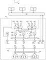
图1示例了根据一个或多个实施例的电子系统1,诸如片上系统(SoC)。电子系统1可以包括各种电子电路,诸如例如:中央处理单元10(CPU,例如,微处理器)、主系统存储器12(例如,系统RAM——随机存取存储器)、直接存储器访问(DMA)控制器14和硬件加速器设备16。Figure 1 illustrates an
硬件加速器设备16可以被设计为支持(基本)算数功能的执行。电子系统1中的电子电路可以通过系统互连网络18(例如,SoC互连)被连接。The
如图1所例示的,硬件加速器设备16可以包括多个处理元件,该多个处理元件包括数目P个处理元件1600、1601、…、160P-1(在本描述中也统称为附图标记160),以及本地数据存储器库的集合,可选地数目Q=2*P个本地数据存储器库M0、…、MQ-1(在本描述中也统称为参考M)。As illustrated in FIG. 1 ,
硬件加速器设备16还可以包括本地控制单元161、本地互连网络162、本地数据存储器控制器163、被耦合到本地只读存储器的集合的本地ROM控制器164、可选地数目P个本地只读存储器1650、1651、…、165P-1(在本描述中也统称为附图标记165),以及被耦合到本地可配置的系数存储器的集合的本地配置存储器控制器166,以及可选地数目P个本地可配置的系数存储器1670、1671、…、167P-1(在本描述中也统称为附图标记167)。存储器167可以包括易失性存储器(例如,RAM存储器)和/或非易失性存储器(例如,PCM存储器)。The
不同的实施例可以包括不同数目P个处理元件160和/或不同数目Q个本地数据存储器库M。举例来说,P可以等于8并且Q可以等于16。Different embodiments may include different numbers P of
处理元件160可以支持(例如,基于适当的静态配置)不同的处理功能(例如,浮点单精度32位、定点/整数32位、或具有并行计算的16位或8位或者矢量模式)。
处理元件160可以包括相应的内部直接存储器访问(DMA)控制器1680、1681、…168P-1(在本描述中也统称为附图标记168)。处理元件160可以被配置为通过相应的直接存储器访问控制器168从本地数据存储器库M和/或从主系统存储器12检索输入数据。处理元件160因此可以处理检索的输入数据以生成输出数据。处理元件160可以被配置为经由相应的直接存储器访问控制器168将处理后的输出数据存储在本地数据存储器库M和/或主系统存储器12中。
附加地,处理元件160可以被配置为从本地只读存储器165和/或从本地可配置系数存储器167检索输入数据以执行这种细化。Additionally,
提供本地数据存储器库M的集合可以促进并行处理数据并且减小存储器访问冲突。本地数据存储器库M可以被设置有缓冲(例如,双缓冲),这可以促进恢复存储器上传时间(写操作)和/或下载时间(读操作)。Providing a set of local data storage banks M can facilitate parallel processing of data and reduce memory access conflicts. The local data store M may be provided with buffering (eg, double buffering), which may facilitate recovery of memory upload times (write operations) and/or download times (read operations).
在实施例中,每个本地数据存储器库可以被复制,使得数据可以从两个存储器库中的一个存储器库被读取,并且(新)数据可以同时被存储在另一个存储器库中(例如,用于稍后处理)。因此,移动数据可能不会对计算性能产生负面影响,这是因为它可能被屏蔽。本地数据存储器库M的双缓冲方案与流模式或背靠背中的数据处理相结合可能是有利的(例如,如适用于被配置为精心设计N个数据输入的连续序列的FFT N点处理器)。In an embodiment, each local data repository can be replicated such that data can be read from one of the two repositories and (new) data can be simultaneously stored in the other (eg, for later processing). Therefore, moving data may not negatively affect computing performance because it may be blocked. The double-buffering scheme of the local data memory bank M may be advantageous in combination with data processing in streaming mode or back-to-back (eg, as applicable to an FFT N-point processor configured to orchestrate a contiguous sequence of N data inputs).
本地控制单元161可以包括寄存器文件,该寄存器文件包括用于设置处理元件160的配置的信息。例如,本地控制单元161可以设置处理元件160以执行由在中央处理单元10上运行的主机应用指示的特定算法。在一个或多个实施例中,本地控制单元161因此可以(例如,动态地)配置处理元件160中的每个处理元件用于计算特定(基本)功能并且可以配置具有特定存储器访问方案和循环周期的相应的内部直接存储器访问控制器168中的每个内部直接存储器访问控制器。The
本地互连网络162可以包括低复杂度互连系统,例如基于已知类型的总线网络(诸如,基于AXI4的互连)。例如,本地互连网络162的数据并行性可以是64位,并且地址宽度可以是32位。The
本地互连网络162可以被配置为将处理元件160连接到本地数据存储器库M和/或主系统存储器12。附加地,本地互连网络162可以被配置为将本地控制单元161和本地配置存储器控制器166连接到系统互连网络18。
在实施例中,互连网络162可以包括:P个主端口MP0、MP1、…、MPP-1的集合(在本描述中也统称为附图标记MP),这些主端口中的每个主端口可耦合到相应的处理元件160;P个从端口SP0、SP1、…SPP-1的集合(在本描述中也统称为附图标记SP),这些从端口中的每个从端口经由本地数据存储器控制器163可耦合到本地数据存储器库M;另一对端口,包括系统主端口MPP和系统从端口SPP,被配置用于耦合到系统互联网络18(例如,以从中央处理单元10接收指令和/或访问存储在系统存储器12中的数据);以及又一从端口SPP+1,被耦合到本地控制单元161并且被耦合到本地配置存储器控制器166。In an embodiment, the
在一个或多个实施例中,互连网络162可以是固定的(即,不可重新配置的)。In one or more embodiments, the
在示例性实施例中(参见,例如在描述的末尾处提供的表I,其中“X”符号指示两个端口之间的现有连接),互连网络162可以实现以下连接:被耦合到处理元件160的P个主端口MP0、MP1、…、MPP-1中的每个主端口可以被连接到被耦合到本地数据存储器控制器163的相应的从端口SP0、SP1、…SPP-1;并且被耦合到系统互连网络18的系统主端口MPP可以被连接到被耦合到本地控制单元161和本地配置存储器控制器166的从端口SPP+1。In an exemplary embodiment (see, eg, Table I provided at the end of the description, where the "X" symbol indicates an existing connection between two ports), the
在另一示例性实施例中(参见,例如在描述的末尾处提供的表II,其中“X”符号指示两个端口之间的现有连接),互连网络162可以进一步实现以下连接:P个主端口MP0、MP1、…MPP-1中的每个主端口可以被连接到被耦合到系统互连网络18的系统从端口SPP。以这种方式,可以经由系统互连网络18在任何处理元件160与SoC之间提供连通性。In another exemplary embodiment (see, eg, Table II provided at the end of the description, where an "X" symbol indicates an existing connection between two ports), the
在另一示例性实施例中(参见,例如在描述的末尾处提供的表III,其中“X”符号指示两个端口之间的现有连接,并且括号之间的“X”指示可选连接),互连网络162可以进一步实现以下连接:被耦合到系统互连网络18的系统主端口MPP可以被连接到从端口SP0、SP1、…、SPP-1中的至少一个从端口(在此,在P个从端口的集合SP0、SP1、…SPP-1中的第一从端口SP0)。以这种方式,可以在主端口MPP与(任何)从端口之间提供连接。根据系统1的具体应用,主端口MPP连接可以被扩展到多个(例如,所有)从端口SP0、SP1、…SPP-1。主端口MPP与从端口SP0、SP1、…SPP-1中的至少一个从端口的连接可以(仅)被用于将要被处理的输入数据加载到本地数据存储器库M0、…MQ-1中,只要所有存储器库可以经由单个从端口被访问。可以仅使用一个从端口来加载输入数据,而通过并行计算来处理数据可以利用使用多个(例如,所有)从端口SP0、SP1、…SPP-1的优势。In another exemplary embodiment (see, eg, Table III provided at the end of the description, where an "X" symbol indicates an existing connection between two ports and an "X" between parentheses indicates an optional connection ), the
在一个或多个实施例中,本地数据存储器控制器163可以被配置为仲裁(例如,通过处理元件160)对本地数据存储器库M的访问。例如,本地数据存储器控制器163可以使用根据从本地控制单元161接收到的信号来选择的存储器访问方案(例如,用于特定算法的计算)。In one or more embodiments, the local
在一个或多个实施例中,根据特定的突发类型、突发长度和存储器访问方案,本地数据存储器控制器163可以将由读取/写入直接存储器访问控制器168生成的输入读取/写入事务突发(例如,AXI突发)转换成读取/写入存储器访问序列。In one or more embodiments, local
在一个或多个实施例中,由处理元件160经由本地ROM控制器164可访问的本地只读存储器165可以被配置为存储用于特定算法或操作(例如,用于FFT计算的旋转因子或其它复杂系数)的实现方式的数字因子和/或固定系数。本地ROM控制器164可以实现特定地址方案。In one or more embodiments, local read-
在一个或多个实施例中,由处理元件160经由本地配置存储器控制器166可访问的本地可配置系数存储器167可以被配置为存储可以由软件配置的与应用有关的数字因子和/或系数(例如,用于实现FIR滤波器或波束成形操作的系数、神经网络的权重等)。本地配置存储器控制器166可以实现特定地址方案。In one or more embodiments, local
在一个或多个实施例中,本地只读存储器165和/或本地可配置系数存储器167可以有利地分成与被包括在硬件加速器设备16中的处理元件160的数目相等的数目P个库。这可以有助于避免并行计算期间的冲突。In one or more embodiments, local read-
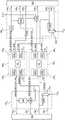
图2是实施例处理元件160和到本地ROM控制器164、本地配置存储器控制器166以及本地数据存储器库M的相关连接的电路框图(其中虚线示意性地指示经由本地互连网络162和本地数据存储器控制器163的处理元件160与本地数据存储器库M之间的可重构连接)。2 is a circuit block diagram of an
如图2所例示的处理元件160可以被配置为:经由相应的读取直接存储器访问2000和缓冲寄存器2020(例如,FIFO寄存器)接收第一输入信号P(例如,指示来自本地数据存储器库M的二进制值的数字信号);经由相应的读取直接存储器访问2001和缓冲寄存器2021(例如,FIFO寄存器)接收第二输入信号Q(例如,指示来自本地数据存储器库M的二进制值的数字信号);接收第一输入系数W0(例如,指示来自本地只读存储器165的二进制值的数字信号);以及接收第二输入系数W1、第三输入系数W2、第四输入系数W3和第五输入系数W4(例如,指示来自本地可配置系数存储器167的相应的二进制值的数字信号)。The
在一个或多个实施例中,处理元件160可以包括与输入信号P、Q的数目相等的数目的读取直接存储器访问200。In one or more embodiments,
应当理解,在不同的实施例中,在处理元件160处接收的输入信号和/或输入系数的数目可以变化。It should be appreciated that the number of input signals and/or input coefficients received at
处理元件160可以包括计算电路20,该计算电路20可配置(可能在运行时)以处理输入值P、Q和输入系数W0、W1、W2、W3、W4以产生第一输出信号X0(例如,指示经由相应的写入直接存储器访问2040和缓冲寄存器2060(诸如,FIFO寄存器)要被存储在本地数据存储器库M中的二进制值的数字信号)和第二输出信号X1(例如,指示经由相应的写入直接存储器访问2041和缓冲寄存器2061(诸如,FIFO寄存器)要被存储在本地数据存储器库M中的二进制值的数字信号)。
在一个或多个实施例中,处理元件160可以包括与输出信号X0、X1的数目相等的数目的写入直接存储器访问204。In one or more embodiments, the
在一个或多个实施例中,读取和/或写入直接存储器访问200、204(其可以被包括在直接存储器访问控制器168中)的编程可以经由接口(例如,AMBA接口)被执行,该接口可以允许访问位于本地控制单元161中的内部控制寄存器。In one or more embodiments, programming to read and/or write direct memory accesses 200, 204 (which may be included in the direct memory access controller 168) may be performed via an interface (eg, an AMBA interface), This interface may allow access to internal control registers located in the
附加地,处理元件160可以包括被耦合到本地ROM控制器164的ROM地址生成器电路208以及被耦合到本地配置存储器控制器166的存储器地址生成器电路210以管理从其检索的数据。Additionally, the
计算电路20可以包括(例如,高度并行化的)处理资源的集合,例如该处理资源包括:四个复数/实数乘法器电路、两个复数加减法电路、两个累加器电路和两个激活非线性函数电路,可重新配置可耦合(例如,通过多路复用器)以形成不同的数据路径,其中不同的数据路径对应于不同的数学运算。
再次参考图1,硬件加速器设备16的一个或多个实施例可以包括多个读取/写入锁步单元,例如数目R=P/2个锁步单元1690、…、169R-1(在本描述中也统称为附图标记169)。Referring again to FIG. 1 , one or more embodiments of
在实施例中,在一个或多个实施例中,每个锁步单元169可以被配置为将一对处理元件160耦合到互连网络162。例如,如图1所例示的,第一锁步单元1690可以被耦合到第一处理元件1600和第二处理元件1601的DMA控制器1680和1681,并且最后的锁步单元169R-1可以被耦合到最后的处理元件160P-1和倒数第二的处理元件160P-2的DMA控制器168P-1和168P-2。In embodiments, each
每个锁步单元169可以(例如,通过设置本地控制单元161的寄存器)被选择性地配置为在相应的处理元件与互连网络之间传递数据,使得在相应的对中的处理元件可以根据两种不同的操作模式操作:在第一模式(“伪锁步模式”)中,两个处理元件并行操作,其中对中的第一处理元件用作“功能”电路,并且对中的第二处理元件用作“影子”电路,该影子电路复制由功能电路执行的操作,使得可以利用功能安全的目标级别(例如,ASIL-D级别)计算与安全有关的算法;并且在第二模式(“高速模式”)中,两个处理元件如由控制单元161指示的那样彼此独立地操作,使得在不满足ASIL-D安全要求的情况下,可以以更高的速度计算与安全无关的算法。Each
因此,当需要高功能安全时,对于硬件加速器设备16中的每对处理元件160,“功能”计算路径和“影子”计算路径可以针对特定方案/算法被动态地可配置。Thus, for each pair of
图3是通过读取锁步单元1690,r和写入锁步单元1690,w被耦合到互连网络162的实施例的处理元件对1600、1601的电路框图。将理解的是,仅为了清楚起见,锁步单元1690的读取和写入部分被示出为单独的电路块,并且在一个或多个实施例中,锁步单元169的读取和写入部分可以在单个电路中被实现。这同样适用于互连网络162,仅为了清楚起见,在图3中利用两个单独的块示出了互连网络162。3 isa block circuit diagram of a pair of processing elements1600 , 1601 of an embodiment coupled to
如图3所例示的,根据一个或多个实施例的硬件加速器16因此可以包括:至少一对处理元件1600、1601,可配置为支持用于数据处理的两条冗余路径(功能路径和影子路径);互连网络162,被配置为支持来自/到功能处理元件和影子处理元件的数据路由;以及用于每对处理元件(功能处理元件和影子处理元件)的读取锁步单元1690,r和写入锁步单元1690,w,该锁步单元被配置为检查和/或保护经由本地互连网络162从/到本地存储器M和/或系统存储器12(端到端)的数据递送。As illustrated in Figure 3, the
在一个或多个实施例中,(由图3中的实线所例示的)功能路径与执行互连访问的主要路径有关,而(由图3中的虚线所例示的)影子路径与冗余路径有关,冗余路径的互连访问以锁步模式被门控。In one or more embodiments, the functional path (illustrated by the solid line in FIG. 3 ) is related to the primary path that performs the interconnect access, while the shadow path (illustrated by the dashed line in FIG. 3 ) is related to the redundant Path dependent, interconnect access to redundant paths is gated in lockstep mode.
作为示例,读取锁步单元1690,r可以提供互连网络162与第一处理元件1600之间的功能读取地址通道RAf以及互连网络162与第二处理元件1601之间的影子读取地址通道RAs(读取突发请求/地址/确认)。读取锁步单元1690,r还可以提供互连网络162与第一处理元件1600之间的功能读取响应通道RRf以及互连网络162与第二处理元件1601之间的影子读取响应通道RRs(读取数据)。As an example, the read lockstep unit 1690,r may provide a functional read address channelRAf between the
仍然作为示例,写入锁步单元1690,w可以提供互连网络162与第一处理元件1600之间的功能写入地址通道Waf以及互连网络162与第二处理元件1601之间的影子写入地址通道WAs(写入突发请求/地址/确认)。写入锁步单元1690,w还可以提供互连网络162与第一处理元件1600之间的功能写入数据通道WDf以及互连网络162与第二处理元件1601之间的影子写入数据通道WDs(写入数据)。写入锁步单元1690,w还可以提供互连网络162与第一处理元件1600之间的功能写入响应通道WRf以及互连网络162与第二处理元件1601之间的影子写入响应通道WRs(写入响应)。Still by way of example, the write lockstep unit 1690,w may provide a functional write address channelWaf between the
如图3所例示的,读取锁步单元1690,r可以包括:被耦合到功能读取地址通道RAf的循环缓冲电路300,被耦合到循环缓冲电路300的输出和影子读取地址通道RAs的比较器和门控电路302,被耦合到功能读取响应通道RRf并且被配置为在功能读取响应通道RRf上生成读取响应(数据通道)的延迟副本,以及被耦合到延迟生成电路308的输出和影子读取响应通道RRs并且由锁步使能信号LSEN控制的多路复用器或门控电路310。As illustrated in FIG. 3, the read lockstep unit 1690,r may include a
在一个或多个实施例中,循环缓冲电路300可以被配置为以锁步模式缓冲功能读取地址通道RAf上的读取请求(地址通道、控制通道)。循环缓冲电路300的控制逻辑可以基于简单的握手机制、请求和确认,这允许支持大多数通信协议(诸如,AXI协议)。新的读取请求(地址通道、控制通道)可以被缓冲,以便稍后(仅)当条目仍然可用时进行比较,否则确认信号可能被保持低电平等待条目变为空闲。(仅)由于来自处理元件1601的读取请求,条目变为空闲。数据比较可以发生在来自1601的读取请求与缓冲器300的第一条目之间的比较器电路302中。所有缓冲条目(每个请求一个条目)在下一个时钟周期处移位一个位置。循环缓冲器电路300在高速模式下可以不被使能,并且在缓冲器内没有存储读取请求。In one or more embodiments,
在一个或多个实施例中,比较器和门控电路302可以被配置为以锁步模式比较存储在缓冲器300内部的功能读取地址通道RAf与影子读取地址通道RAs之间的读取请求(地址通道、控制通道),并且被配置为将在影子读取地址通道RAs上的请求选通到不允许被传播的互连162。由于锁步模式不被激活,比较器和门控电路302可以将影子读取地址通道RAs上的请求传播到本地互连162,并且数据比较可能不发生。In one or more embodiments, the comparator and
在一个或多个实施例中,读取锁步单元1690,r可以被配置为在由比较器和门控电路302检测到故障的情况下向故障收集单元(FCU)发送故障信号。In one or more embodiments, the
在一个或多个实施例中,由于锁步模式被使能(例如,LSEN=1),多路复用器或门控电路310可以将来自功能读取响应通道RRf(延迟生成电路308的输出)的延迟响应传播到处理元件1601。否则,由于锁步模式被禁用(例如,LSEN=0),多路复用器或门控电路310可以将影子读取响应通道RRS上的响应传播到处理元件1601。In one or more embodiments, since lockstep mode is enabled (eg, LSEN = 1 ), the multiplexer or
如图3所例示的,写入锁步单元1690,w可以包括:被耦合到功能写入地址通道WAf的第一循环缓冲电路312,被耦合到功能写入数据通道WDf的第二循环缓冲电路314,第一比较器,以及被耦合到第一循环缓冲电路312的输出和影子写入地址通道WAs的门控电路316,被耦合到第二循环缓冲电路314的输出和影子写入数据通道WDs的第二比较器和门控电路318,被耦合到功能写入响应通道WRf并且被配置为在功能写入响应通道WRf上生成写入响应(数据通道)的延迟的副本的延迟生成电路326,以及被耦合到延迟生成电路326的输出和影子写入响应通道WRs并且由锁步使能信号LSEN控制的多路复用器或门控电路328。As illustrated in FIG. 3, write lockstep unit 1690,w may include a first
在一个或多个实施例中,第一循环缓冲电路312可以被配置为以锁步模式在功能写入地址通道WAf上缓冲写入请求(地址通道、控制通道)。第一循环缓冲电路312的控制逻辑可以基于简单的握手机制、请求和确认,其允许支持大多数通信协议(诸如,AXI协议)。新的写入请求(地址通道、控制通道)可以被缓冲,以便稍后(仅)当条目仍然可用时进行比较,否则确认信号可能保持低电平,等待条目变为空闲。(仅)由于来自处理元件1601的写入请求,条目变为空闲。数据比较可以发生在来自1601的写入请求与缓冲器312的第一条目之间的比较电路316中。所有缓冲条目(每个请求一个条目)在下一个时钟周期处移位一个位置。第一循环缓冲电路312在高速模式下可以不被使能,使得写入请求不被存储在缓冲器312内并且可以被直接地传播到本地互连162。In one or more embodiments, the first
在一个或多个实施例中,第一比较器和门控电路316可以被配置为以锁步模式比较存储在缓冲器312内部的功能写入地址通道WAf与影子写入地址通道WAs之间的写入请求(地址通道、控制通道),并且将影子写入地址通道WAs上的请求选通到不准被传播的互连162。由于锁步模式不被激活,第一比较器和选通电路316可以将影子写入地址通道WAs上的请求传播到本地互连162,并且数据比较可能不发生。In one or more embodiments, the first comparator and
在一个或多个实施例中,第二循环缓冲电路314可以被配置为以锁步模式缓冲功能写入数据通道WDf上的写入请求(数据通道)。第二循环缓冲电路314的控制逻辑可以基于简单的握手机制、请求和确认,这允许支持大多数通信协议(诸如,AXI协议)。新的写入请求(数据通道)可以被缓冲,以便稍后(仅)当条目仍然可用时进行比较,否则确认信号可能保持低电平,等待条目变为空闲。(仅)由于来自处理元件1601的写入请求,条目变为空闲。数据比较可以发生在来自1601的写入请求与缓冲器314的第一条目之间的比较电路318中。所有缓冲条目(每个请求一个条目)在下一个时钟周期处移位一个位置。第二循环缓冲电路314在高速模式下可以不被使能,使得写入请求不被存储在缓冲器314内并且可以被直接地传播到本地互连162。In one or more embodiments, the second
在一个或多个实施例中,第二比较器和门控电路318可以被配置为以锁步模式比较存储在缓冲器314、影子写入数据通道WDs内部的功能写入数据通道WDf之间的写入请求(数据通道),并且将影子写入数据通道WDs上的请求选通到不准被传播的互连162。由于锁步模式不被激活,第二比较器和门控电路318可以将影子写入数据通道WDs上的请求传播到本地互连162,并且数据比较可能不发生。In one or more embodiments, the second comparator and
在一个或多个实施例中,写入锁步单元1690,w可以被配置为在由比较器和门控电路316和/或318检测到故障的情况下向故障收集单元发送故障信号。附加地或备选地,比较器和门控电路316和/或318可以被配置为选通功能路径WAf和WDf上的写入访问以便避免在检测到故障的情况下破坏存储器内容。In one or more embodiments, the
因此,在一个或多个实施例中,功能读取访问可以被立即传播到互连网络162而无需等待在比较电路302中发生比较,而功能写入访问仅在比较器电路316和/或318中已经发生比较之后可以被传播到互连网络162,只要错误的写入访问可能破坏存储在存储器中的数据。Thus, in one or more embodiments, functional read accesses may be propagated to
在一个或多个实施例中,当硬件加速器设备16被用于与安全有关的应用时,每对处理元件160(静态地被定义在硬件加速器设备16内)可以被编程为通过在控制单元161的配置寄存器中设置相应的配置位来根据伪锁步模式进行操作。例如,如果这种配置位具有第一值(例如,它等于1),则读取/写入比较器电路302、316、318可以在DMA读取/写入输出通道上执行比较。响应于检测到失配,对应的写入请求可以不被传播,流可以被停止,并且错误可以被报告给片上系统1的(例如,外部)逻辑故障收集单元(LFCU)。备选地,如果这种配置具有第二值(例如,它等于0),则总线上的请求可以简单地被传播到存储器控制器163。In one or more embodiments, when
在一个或多个实施例中,当对中的两个处理元件(即,“功能”处理元件1600和“影子”处理元件1601)以伪锁步模式操作时,它们的操作可以是(例如,异相的)时移的。例如,这种时移可以等于一定数目的时钟周期,可选地两个时钟周期。例如,如图4所例示的,这可以通过硬件架构获得。In one or more embodiments, when two processing elements in a pair (ie, "functional" processing element1600 and "shadow" processing element1601 ) operate in pseudo lockstep mode, their operation may be ( For example, out-of-phase) time-shifted. For example, this time shift may be equal to a certain number of clock cycles, optionally two clock cycles. For example, as illustrated in Figure 4, this can be achieved by a hardware architecture.
在一个或多个实施例中,对于所有的内部DMA控制器(例如,读取DMA控制器和写入DMA控制器两者),相移机制可以是相同的。这种时移可以促进对共因故障的良好覆盖。例如,由于电磁干扰(EMI)导致的故障可能导致对于功能路径和影子路径两者都出现故障,如果没有时移,则锁步单元将无法检测到该故障。In one or more embodiments, the phase shift mechanism may be the same for all internal DMA controllers (eg, both read DMA controllers and write DMA controllers). This time shift can facilitate good coverage of common cause faults. For example, a failure due to electromagnetic interference (EMI) can cause a failure for both the functional and shadow paths, which the lockstep unit would not be able to detect without time shifting.
如图4所例示的,被配置为一对功能处理元件的处理元件1600的DMA控制器1680(读取和/或写入)可以从控制单元161接收开始信号START0。被配置为一对影子处理元件的处理元件1601的DMA控制器1681(读取和/或写入)可以由于伪锁步模式被使能(例如,LSEN=1)来接收开始信号START0的延迟副本START0’,或者由于高速模式被使能(例如,LSEN=0)来接收来自控制单元161的开始信号STATR1。延迟生成电路块400可以接收开始信号STRAT0并且生成延迟副本START0’。选择电路402(例如,多路复用器或门控电路)可以根据伪锁步使能信号LSEN来将延迟副本START0’或开始信号START1传播到DMA控制器1681。As illustrated in FIG. 4 , the DMA controller 1680 (read and/or write) of the
在一个或多个实施例中,当对中的两个处理元件在高速模式下操作时,读取/写入锁步单元169可以被配置为基本安全机制(没有锁步比较器,即提供两个独立的数据路径)以(仅)保护经由本地互连162到/从本地存储器M的(端到端)数据传递。In one or more embodiments, the read/
在一个或多个实施例中,硬件加速器设备16可以支持多个算法的并发执行。在这种情况下,处理元件的对应的对可以被配置为根据特定算法的安全要求以伪锁步模式或高速模式操作。在实施例中,处理元件对的子集可以以伪锁步模式操作,而处理元件对的另一子集可以以高速模式操作。伪锁步模式或高速模式可以是硬件加速器设备16的配置的一部分并且可以是基于算法可选择的。In one or more embodiments,
附加地或备选地,在一个或多个实施例中,可以在处理元件160与可配置的系数存储器167之间的数据路径中实现类似的安全机制。Additionally or alternatively, in one or more embodiments, similar security mechanisms may be implemented in the data path between
例如,图5是可配置的系数存储器167的实施例实现细节的电路框图。如图5所例示的,每个处理元件160可以包括被耦合到存储器控制器166的相应的存储器地址生成器电路210,可配置的系数存储器167被耦合到该存储器控制器166。在图3中图示的相同的读取锁步单元169r可以被耦合到存储器地址生成器电路210以在功能路径与影子路径之间比较系数存储器167中的读取请求。被用于DMA控制器168的相同的开始信号START0可以被用于存储器地址生成器电路210。For example, FIG. 5 is a circuit block diagram of implementation details of an embodiment of the
附加地或备选地,在一个或多个实施例中,可以在处理元件160与只读存储器165之间的数据路径中实现类似的安全机制。Additionally or alternatively, in one or more embodiments, similar security mechanisms may be implemented in the data path between
例如,每个处理元件160可以包括被耦合到ROM控制器164的相应的ROM地址生成器电路208,只读存储器165被耦合到ROM控制器164。在图3中图示的相同的读取锁步单元169r可以被耦合到ROM地址生成器电路208,以在功能路径与影子路径之间比较只读存储器165中的读取请求。被用于DMA控制器168的相同的开始信号START0可以被用于ROM地址生成器电路208。For example, each
在一个或多个实施例中,硬件加速器设备16可以通过由保护代码(诸如,双错误检测(DED)、单纠错和双纠错(SECDED)和/或PARITY码)保护(所有)地址和存储(在RAM存储器中和/或在ROM存储器中)的数据来符合ISO 26262安全标准的要求。In one or more embodiments,
在一个或多个实施例中,本地互连162的控制信号(例如,突发长度信号、突发类型信号等)可以由DED或PARITY码保护。附加地,PARITY位可以被用于保护本地互连握手位。In one or more embodiments, control signals (eg, burst length signals, burst type signals, etc.) of
在一个或多个实施例中,读取/写入DMA控制器168、本地数据存储器控制器163、可配置的存储器控制器166和/或ROM存储器控制器164因此可以实现新的功能以提供改进的功能安全。In one or more embodiments, read/write
在一个或多个实施例中,保护方案可以是根据处理系统1的要求静态地可配置的。In one or more embodiments, the protection scheme may be statically configurable according to the requirements of the
在一个或多个实施例中,读取DMA控制器200可以被配置为实现以下一个或多个功能:在突发起始地址上生成DED、SECDED或PARITY码,在突发控制信号上生成DED或PARITY码,在输出握手信号上生成PARITY位,对输入的读取数据进行DED、SECDED或PARITY检查,并且向逻辑故障收集单元(LFCU)发出错误信令,以及对输入握手信号进行PARITY检查,以及向逻辑故障收集单元发出错误信令。In one or more embodiments, read
例如,如图3所例示的,读取DMA控制器200可以包括:相应的保护代码生成器电路304,被配置为在功能读取地址通道RAf上生成读取请求的保护代码(地址通道、控制通道);以及相应的保护代码检查器电路306,被配置为检查在功能读取响应通道RRf上的读取响应(数据通道)的保护代码以及在影子读取响应通道RRs上的(具有延迟的)数据通道的复制。For example, as illustrated in FIG. 3, the
在一个或多个实施例中,写入DMA控制器204可以被配置为实现以下一个或多个功能:在突发起始地址上生成DED、SECDED或PARITY码,在输出握手信号上生成PARITY位,在写入数据上生成DED、SECDED或PARITY码,以及对输入握手信号进行PARITY检查,以及向逻辑故障收集单元发出错误信令。In one or more embodiments, the
例如,如图3所例示的,写入DMA控制器204可以包括:相应的保护代码生成器电路320,被配置为在功能写入地址通道WAf上生成写入请求(地址通道、控制通道)的保护代码,和/或被配置为在功能写入数据通道WDf上生成写入请求(数据通道)的保护代码;以及相应的保护代码检查器电路324,被配置为检查功能写入响应通道WRf上的写入响应的保护代码以及影子写入响应通道WRs上的(具有延迟的)响应通道的复制。For example, as illustrated in FIG. 3, the
在一个或多个实施例中,本地数据存储器控制器163可以被配置为实现以下一个或多个功能:对输入突发起始地址进行DED、SECDED或PARITY检查,以及向逻辑故障收集单元发送错误信令,向存储器库M传播WRITE DATA保护代码,对输入控制信号进行DED或PARITY检查,将来自存储器库M的READ DATA ECC保护代码传播到本地互连162,对输入握手信号进行PARITY检查,以及向逻辑故障检查单元发送错误信令,以及在输出握手信号上生成PARITY位。In one or more embodiments, the local
在一个或多个实施例中,可配置的存储器地址生成器电路210可以被配置为实现以下一个或多个功能:在地址上生成DED、SECDED或PARITY码,在突发控制信号上生成DED或PARITY码,在输出握手信号上生成PARITY位,以及对输入握手信号进行PARITY检查,以及向逻辑故障收集单元发送错误信令。In one or more embodiments, the configurable memory
在一个或多个实施例中,可配置的存储器控制器166可以被配置为实现以下一个或多个功能:对输入突发起始地址进行DED、SECDED或PARITY检查,以及向逻辑故障收集单元发送错误信令,对读取数据值进行DED、SECDED或PARITY检查,以及向逻辑故障收集单元发送错误信令,对输入本地总线控制信号进行DED或PARITY检查,以及向逻辑故障收集单元发送错误信令,对输入握手信号进行PARITY检查,以及向逻辑故障收集单元发送错误信令,以及在输出握手信号上生成PARITY位。In one or more embodiments, the
在一个或多个实施例中,ROM地址生成器208可以被配置为在地址上实现DED、SECDED或PARITY码的生成。In one or more embodiments, the
在一个或多个实施例中,ROM控制器164可以被配置为实现以下一个或多个功能:对输入地址进行DED、SECDED或PARITY检查,向逻辑故障收集单元发送错误信令,以及对读取数据值进行DED、SECDED或PARITY检查,以及向逻辑故障收集单元发送错误信令。In one or more embodiments,
需要注意的是,纠错码(ECC)保护方案可以在地址路径和数据路径上提供高覆盖率,但是它们可能不适用于接口的控制路径。目标接口(例如,存储器)上的控制信号可以由逻辑块(例如,FSM、解码器等)生成,而无需在启动程序接口(例如,内部DMA、外部AXI接口)上保留源信息。Note that error-correcting code (ECC) protection schemes can provide high coverage on the address and data paths, but they may not be suitable for the control path of an interface. Control signals on target interfaces (eg, memory) can be generated by logic blocks (eg, FSM, decoders, etc.) without maintaining source information on initiator interfaces (eg, internal DMA, external AXI interface).
因此,一个或多个实施例可以包括(甚至独立于如先前描述的锁步架构的实现)存储器读取/写入看门狗机制以提供控制路径上的端到端(例如,启动程序存储器(诸如,DMA存储器))安全机制,该控制路径可以有助于检测存储器控制器的控制逻辑内部的硬故障和/或软故障。Thus, one or more embodiments may include (even independently of the implementation of the lockstep architecture as previously described) a memory read/write watchdog mechanism to provide end-to-end (eg, boot program memory ( Such as, DMA memory)) safety mechanisms, the control path can help detect hard and/or soft faults within the control logic of the memory controller.
在一个或多个实施例中,第一类型的存储器读取/写入看门狗可以被配置为由特定的启动程序(例如,每个启动程序)对在算法(例如,每个算法)的计算期间执行的存储器操作的数目和/或类型(读取、写入、总线宽度)进行计数。In one or more embodiments, the first type of memory read/write watchdog can be configured to be controlled by a specific initiator (eg, each initiator) on the algorithm (eg, each algorithm) The number and/or type (read, write, bus width) of memory operations performed during the computation is counted.
需要注意的是,与其中存储器访问取决于策略、编译工具链等的内核实现的解决方案相反,由硬件加速器设备在存储器中执行的数据流和操作的数目/类型是根据计算的算法静态地定义的。It is important to note that, in contrast to the kernel-implemented solution where memory access depends on policy, compilation toolchain, etc., the number/type of data streams and operations performed in memory by the hardware accelerator device is statically defined according to the algorithm of the computation of.
因此,一个或多个实施例可以包括针对每个目标接口(例如,本地存储器或系统存储器)的读取/写入看门狗电路,该读取/写入看门狗电路包括每个启动程序设备一组并发读取/写入计数器(例如,针对每个内部DMA控制器的计数器、针对每个外部总线接口的计数器等)。每个读取/写入看门狗电路可以跟踪所有的操作并且将累积的结果存储在状态寄存器的集合中。在算法的执行结束时,可以将看门狗状态寄存器的内容与预期数目的读取/写入操作进行比较,从而提供防止控制路径可能出现故障的安全机制。Thus, one or more embodiments may include a read/write watchdog circuit for each target interface (eg, local memory or system memory) that includes each boot program A device set of concurrent read/write counters (eg, counters for each internal DMA controller, counters for each external bus interface, etc.). Each read/write watchdog circuit can track all operations and store the accumulated results in a set of status registers. At the end of the execution of the algorithm, the contents of the watchdog status register can be compared to the expected number of read/write operations, providing a safety mechanism against possible failure of the control path.
图6A是在一个或多个实施例中使用的这种第一类型的存储器看门狗的示例电路框图。如图6A所例示的,存储器看门狗电路60A可以包括读取计数器电路62Ar和写入计数器电路62Aw。6A is an example circuit block diagram of this first type of memory watchdog used in one or more embodiments. As illustrated in FIG. 6A, the
读取计数器电路62Ar可以被配置为接收相应的芯片选择信号CS、读取使能信号REN以及相应的标识信号ID,其携带适合于标识启动程序的信息(例如,启动程序ID)。读取计数器电路62Ar可以被配置为生成(例如,要被传播到本地控制单元161中的看门狗状态寄存器的)输出读取计数信号RC。Read counter circuit 62Ar may be configured to receive corresponding chip select signal CS, read enable signal REN, and corresponding identification signal ID carrying information suitable for identifying a boot program (eg, boot program ID). Read counter circuit 62Ar may be configured to generate an output read count signal RC (eg, to be propagated to a watchdog status register in local control unit 161).
写入计数器电路62Aw可以被配置为接收相应的芯片选择信号CS、写入使能信号WEN、以及携带适用于标识启动程序的信息的相应的标识信号ID(例如,启动程序ID)。写入计数器电路62Aw可以被配置为生成(例如,要被传播到本地控制单元161中的看门狗状态寄存器的)输出写入计数信号WC。Write counter circuit 62Aw may be configured to receive corresponding chip select signal CS, write enable signal WEN, and corresponding identification signal ID (eg, boot program ID) carrying information suitable for identifying a boot program. Write counter circuit 62Aw may be configured to generate an output write count signal WC (eg, to be propagated to a watchdog status register in local control unit 161).
在一个或多个实施例中,本地存储器读取/写入看门狗电路60A可以被配置为:基于算法针对(基于接收到的启动程序ID的)每个启动程序跟踪(例如,累积的)读取访问的次数,基于算法针对(基于接收到的启动程序ID的)每个启动程序跟踪(例如,累积的)写入访问的次数,并且可选地,在故障的情况下向逻辑故障收集单元发出故障信号。In one or more embodiments, the local memory read/
在一个或多个实施例中,如图6A所例示的,可以根据不同的策略检查看门狗状态。那些策略可以是经由本地控制单元的控制寄存器可配置的。例如,看门狗状态检查策略可以包括在针对配置的算法的数据处理结束时的看门狗状态的软件检查。在另一示例中,看门狗状态检查策略可以包括每存储器库和每启动程序的预期数目的读取/写入访问的(例如,在针对配置的算法的数据处理结束时自动触发的)硬件检查,可选地具有在故障的情况下向逻辑故障收集单元发送错误信令。In one or more embodiments, as illustrated in Figure 6A, the watchdog status can be checked according to different strategies. Those policies may be configurable via the control registers of the local control unit. For example, a watchdog status check policy may include a software check of the watchdog status at the end of data processing for the configured algorithm. In another example, a watchdog status check policy may include hardware per memory bank and per boot program an expected number of read/write accesses (eg, automatically triggered at the end of data processing for a configured algorithm) Checking, optionally with error signaling to the logical fault collecting unit in the case of a fault.
纯粹地作为非限制性示例,参考涉及单个处理元件160的矩阵乘法算法来举例说明参考图6A公开的存储器看门狗机制的操作。矩阵乘法算法可以被指示为C[n,n]=A[n,n]*B[n,n]。输入矩阵A和B可以由系统DMA控制器14预加载在本地存储器M中。输出矩阵C可以由处理元件160的内部DMA控制器168存储在本地存储器M中。因此,由系统DMA控制器执行的写入操作的预期数目等于2*(n*n),由内部DMA控制器执行的读取操作的预期数目等于2*(n*n*n),并且由内部DMA控制器执行的写入操作的预期数目等于n*n。Purely as a non-limiting example, the operation of the memory watchdog mechanism disclosed with reference to FIG. 6A is illustrated with reference to a matrix multiplication algorithm involving a
附加地或备选地,在一个或多个实施例中,第二类型的存储器读取/写入看门狗可以被配置为在由特定启动程序(例如,每个读取或写入内部DMA)计算算法(例如,每个算法)期间对未完成的存储器操作的数目进行计数,其中当发出事务时增加这种数目并且当接收到响应时减小这种数目。因此,第二类型的存储器读取/写入看门狗可能不对存储器访问的绝对值而是(例如,通过简单的升降计数器电路)对存储器访问的相对值进行计数,该相对值在算法结束时预期等于零。Additionally or alternatively, in one or more embodiments, a second type of memory read/write watchdog may be configured to be executed by a specific initiator (eg, each read or write internal DMA). ) counts the number of outstanding memory operations during an algorithm (eg, each algorithm), where this number is incremented when a transaction is issued and decremented when a response is received. Therefore, a second type of memory read/write watchdog may not count the absolute value of memory accesses but (eg, by a simple up-down counter circuit) the relative value of memory accesses, which is at the end of the algorithm Expected to be equal to zero.
图6B是在一个或多个实施例中使用的这种第二类型的存储器看门狗的示例电路框图。如图6B所例示的,存储器看门狗电路60B可以包括读取升降计数器电路62Br和/或写入升降计数器电路62Bw,其被配置为对由每个启动程序请求要读取或写入的字的数目与实际读取或写入的字的数目之间的差异进行计数。6B is an example circuit block diagram of this second type of memory watchdog used in one or more embodiments. As illustrated in FIG. 6B ,
读取升降计数器电路62Br可以被配置为接收相应的读取使能信号REN和/或读取突发长度信号RBURSTL以增加相应的计数器值,并且接收相应的响应使能信号RRESP_EN以减小相应的计数器值。因此,如果启动程序接口是读取接口(例如,本地读取DMA接口),则读取请求和突发长度信号可以被用于递增操作,而响应使能信号(其可以被用于检测有效读取数据)可以被用于递减升降计数器值。在该示例性情况下,由看门狗电路使用的所有的信号都来自相同的启动程序接口。The read up-down counter circuit 62Br may be configured to receive the corresponding read enable signal REN and/or the read burst length signal RBURSTL to increment the corresponding counter value, and to receive the corresponding response enable signal RRESP_EN to decrement the corresponding counter value. counter value. Thus, if the initiator interface is a read interface (eg, a local read DMA interface), the read request and burst length signals can be used for increment operations, while the response enable signal (which can be used to detect valid reads) fetch data) can be used to decrement the up-down counter value. In this exemplary case, all the signals used by the watchdog circuit come from the same initiator interface.
写入升降计数器电路62Bw可以被配置为接收相应的写入使能信号WEN和/或写入突发长度信号WBURSTL以增加相应的计数器值,并且接收相应的写入使能信号W_EN和/或以及携带适用于标识启动程序(例如,启动程序ID)的信息的相应的标识信号INIT_ID以减小相应的计数器值。因此,如果启动程序接口是写入接口(例如,本地写入DMA接口),则写入请求和突发长度信号可以被用于递增请求要被写入的字的数目,而写入使能信号(其被用于检测有效数据)和目标接口(例如,存储器控制器输出)处的启动程序ID可以被用于递减字的数目。The write up-down counter circuit 62Bw may be configured to receive the corresponding write enable signal WEN and/or the write burst length signal WBURSTL to increment the corresponding counter value, and to receive the corresponding write enable signal W_EN and/or and A corresponding identification signal INIT_ID carrying information suitable for identifying the initiator (eg, the initiator ID) to decrement the corresponding counter value. Thus, if the initiator interface is a write interface (eg, a local write DMA interface), the write request and burst length signals can be used to increment the number of words requested to be written, while the write enable signal (which is used to detect valid data) and the initiator ID at the target interface (eg, memory controller output) can be used to decrement the number of words.
在一个或多个实施例中,启动程序ID可以从每个源(例如,使用AXI用户信号)被传播到目标,以用于保护硬件加速器设备内部的写入事务。In one or more embodiments, the initiator ID may be propagated from each source (eg, using AXI user signals) to the target for use in securing write transactions inside the hardware accelerator device.
在数据处理结束时(例如,在算法的计算结束时),外部主机控制器可以读取(例如,每个启动程序一个)实例化看门狗的状态并且验证最终计数值是否等于零。请求的数目与数据实际读取/写入的数目之间的不匹配可以归因于控制器内部的故障(例如,单点故障,SPF)。At the end of data processing (eg, at the end of an algorithm's computation), the external host controller can read (eg, one per boot program) the status of the instantiated watchdogs and verify that the final count value equals zero. The mismatch between the number of requests and the number of actual reads/writes of data can be attributed to failures within the controller (eg, single point of failure, SPF).
在一个或多个实施例中,如图6B所例示的,可以根据不同的策略检查看门狗状态。那些策略可以是经由本地控制单元的控制寄存器可配置的。例如,看门狗状态检查策略可以包括在用于配置的算法的数据处理结束时(当未完成的事务预期为零时)看门狗状态的软件检查。在另一示例中,看门狗状态检查策略可以包括每个存储器库和每个启动程序的预期数目的未完成的事务的(例如,在用于配置的算法的数据处理结束时自动触发的)硬件检查,可选地具有在故障的情况下向逻辑故障收集单元发送的错误信令。在另一示例中,看门狗状态检查策略可以包括通过在可配置的阈值上断言的中断来监测硬件或软件运行时间,作为性能度量(等待时间、未完成的事务的峰值/平均值)。In one or more embodiments, as illustrated in Figure 6B, the watchdog status can be checked according to different strategies. Those policies may be configurable via the control registers of the local control unit. For example, a watchdog status checking strategy may include a software check of the watchdog status at the end of data processing for the configured algorithm (when outstanding transactions are expected to be zero). In another example, the watchdog status check policy may include an expected number of outstanding transactions per memory bank and per initiator (eg, triggered automatically at the end of data processing for the configured algorithm) Hardware check, optionally with error signaling to the logical failure collection unit in case of failure. In another example, a watchdog status checking strategy may include monitoring hardware or software runtime by interrupts asserted at configurable thresholds as a performance measure (latency, peak/average of outstanding transactions).
需要注意的是,图6B所例示的看门狗机制依赖于对未完成的事务的数目而不是有效的事务的总数目进行计数,可以提供以下一个或多个优点:应用程序级别的简单和即时的看门狗管理(无需为每个算法配置事务的绝对值),对于那些存储器访问的数目取决于数据的类型/值的算法的弹性,以及作为附加的性能度量的未完成的事务的峰值/平均值的运行时间监测。Note that the watchdog mechanism illustrated in Figure 6B, which relies on counting the number of outstanding transactions rather than the total number of active transactions, may provide one or more of the following advantages: Simple and immediate application level watchdog management (no need to configure an absolute value of transactions for each algorithm), algorithm resilience for those where the number of memory accesses depends on the type/value of the data, and as an additional performance measure the peak of outstanding transactions/ Average runtime monitoring.
在一个或多个实施例中,提供如图6A或图6B所例示的存储器读取/写入看门狗电路可以有助于总体安全目标(本地存储器库M、配置存储器167和只读存储器165),而避免内部存储器控制器的复制并且在这种块的内部达到令人满意的单点故障(SPF)覆盖率。In one or more embodiments, providing a memory read/write watchdog circuit as exemplified in FIG. 6A or FIG. 6B may facilitate overall security goals (local memory bank M,
需要注意的是,在常规的设备中,安全监测器通常通过它们的复制(例如,在标准内核的情况下)或通过被施加到完全/部分设备的逻辑内置自测试(LBIST)程序来保护安全监测器免受潜在故障的影响。It should be noted that in conventional devices, security monitors are usually secured by their duplication (eg, in the case of standard kernels) or by logic built-in self-test (LBIST) procedures applied to full/partial devices Monitors are protected from potential failures.
为了减少由于监测器或LBIST插入流程的重复而导致的面积开销和/或设计复杂度,一个或多个实施例可以包括(甚至独立于锁步架构或如先前描述的存储器看门狗机制的实现的)用于安全监测器的专用硬件内置自测试(BIST)。在一个或多个实施例中,就常规的设备在LBIST的执行期间和下一次部分或完全复位期间可能不可用而言,这种专用硬件BIST还可以减少设备功能的不可用性。To reduce area overhead and/or design complexity due to duplication of monitor or LBIST insertion flows, one or more embodiments may include (even independent of lockstep architecture or implementation of a memory watchdog mechanism as previously described) ) Dedicated hardware built-in self-test (BIST) for safety monitors. In one or more embodiments, such a dedicated hardware BIST may also reduce the unavailability of device functionality to the extent that conventional devices may be unavailable during the execution of the LBIST and during the next partial or full reset.
在一个或多个实施例中,专用硬件BIST可以提供以下一个或多个特征:用于安全监测器的潜在故障(LF)检测或故障注入以检查到LFCU接口的监测器,(例如,具有在应用程序级别定义的速率时间的)运行时间检查,以及BIST和安全监测器的故障模拟以提供所需的固定覆盖率(例如,等于或高于用于ASIL-D安全级别的90%的覆盖率)。In one or more embodiments, a dedicated hardware BIST may provide one or more of the following features: latent fault (LF) detection or fault injection for safety monitors to check monitors that interface to the LFCU, (eg, with Application-level defined rate time) runtime checking, and fault simulation of BIST and safety monitors to provide the required fixed coverage (e.g., equal to or higher than 90% coverage for ASIL-D safety levels) ).
在一个或多个实施例中,BIST可以被施加到所有被实现的安全监测器以支持端到端保护方案、锁步比较器、存储器看门狗等。In one or more embodiments, BIST may be applied to all implemented safety monitors to support end-to-end protection schemes, lockstep comparators, memory watchdogs, and the like.
图7是根据一个或多个实施例的实施例硬件安全监测器BIST的电路框图。如图7所例示的硬件BIST可以包括:本地控制单元161;基于ROM、查找表或伪随机线性反馈移位寄存器(LFSR)的模式发生器71或故障注入器71;加法器节点72,被配置为将从功能路径接收的数据与模式发生器/故障注入器71产生的数据相结合;选择电路73(例如,多路复用器),被配置为将来自加法器节点72的输出数据或来自模式发生器/故障注入器71的输出数据传播到安全监测器74,其中可以选择安全监测器的子集(例如,全部、单个、序列)用于BIST过程的执行;安全监测器节点(测量点)的子集的CRCn(例如,CRC32、CRC16等)压缩器75;比较器电路块77,被配置为将CRCn压缩器75的输出与最终签名76(例如,魔术(magic)值)和/或中间值进行比较以增加覆盖范围故障信令;控制和状态寄存器;以及到逻辑故障收集单元的接口78。7 is a circuit block diagram of an embodiment hardware security monitor BIST in accordance with one or more embodiments. A hardware BIST as illustrated in FIG. 7 may include: a
在一个或多个实施例中,硬件加速器设备的功能在安全监测器BIST的执行期间的运行时间可能不可用。In one or more embodiments, the functionality of the hardware accelerator device may not be available at runtime during execution of the security monitor BIST.
在一个或多个实施例中,在安全监测器BIST的执行之后可能需要硬件加速器设备的复位。In one or more embodiments, a reset of the hardware accelerator device may be required after execution of the safety monitor BIST.
由于本地控制单元161可以表示用于硬件加速器设备16的故障源,因此一个或多个实施例可以依赖于以下一个或多个安全机制:FSM和关键部分(状态/错误寄存器、中断等)的复制,以及用于控制寄存器(奇偶校验位或CRC32校验和)的保护代码。Since the
在一个或多个实施例中,接口78可以包括(简单的)双信号电平注册接口。如果在硬件加速器设备中检测到至少一个不可校正的错误,则可以断言(例如,设置为逻辑电平1)第一信号(例如,EDPA_cf)。如果在硬件加速器设备内部检测到至少一个可校正的错误,则可以断言(例如,设置为逻辑电平1)第二信号(例如,EDPA_ncf)。因此,接口78可以有利地从外部发信号通知内部检测到的错误以让系统(例如,片上系统)在由安全目标要求的可接受的时间间隔(容错时间间隔)内达到安全状态。In one or more embodiments,
在一个或多个实施例中,电子系统1可以被实现为单个硅芯片或管芯中的集成电路(例如,作为片上系统)。备选地,电子系统1可以包括分布式系统,该分布式系统包括(例如,通过印刷电路板(PCB))互连在一起的多个集成电路。In one or more embodiments,
因此,例如,当需要计算与安全有关的算法时,如本文所例示的一个或多个实施例可以提供硬件加速器设备16,其可以被选择性地配置为(例如,在运行时)在功能安全的某一级别处(例如,在ASIL-D级别处)操作。当需要计算与安全无关的算法时,可以加速这种计算,所有内部计算能力都可用。Thus, for example, when computing safety-related algorithms is required, one or more embodiments as exemplified herein may provide a
本文公开的功能安全架构有助于提供基于存储器的硬件加速器设备,并且可能提供集成硬件加速器设备的SoC,其支持具有减少的面积开销的ASIL-D应用。The functional safety architecture disclosed herein facilitates providing memory-based hardware accelerator devices, and possibly SoCs integrating hardware accelerator devices, that support ASIL-D applications with reduced area overhead.
如本文所例示的,硬件加速器设备(例如,16)可以包括:被布置在处理电路的子集(例如,对)中的处理电路(例如,160)的集合;被耦合到存储器控制器(例如,163)的数据存储器库(例如,M)的集合;包括提供用于处理电路的配置数据的存储空间的配置寄存器的控制单元(例如,161);以及互连网络(例如,162)。可以根据存储在控制单元中的配置数据来配置处理电路,以经由互连网络和存储器控制器从数据存储器库读取(例如,200、202)第一输入数据,处理(例如,20)第一输入数据以产生输出数据,以及经由互连网络和存储器控制器将输出数据写入(例如,204、206)数据存储器库中。硬件加速器设备可以包括可配置的锁步控制单元的集合(例如,169),该可配置的锁步控制单元将处理电路(例如,DMA控制器168)接口连接到互连网络,可配置的锁步控制单元的集合中的每个可配置的锁步控制单元(例如,1690)被耦合到处理电路的集合中的处理电路(例如1600、1601)的子集。每个可配置的锁步控制单元可以被选择性地激活(例如,LSEN)以:在第一操作模式(例如,“锁步模式”或“伪锁步模式”)下操作,其中锁步控制单元(例如,1690,r、1690,w)被配置为将由处理电路的相应的子集中的第一处理电路(例如,1600)和第二处理电路(例如,1601)朝向存储器控制器发出的数据读取请求和/或数据写入请求进行比较以检测故障;或者在第二操作模式(例如,“高速模式”或“性能模式”)下操作,其中锁步控制单元被配置为朝向存储器控制器传播由处理电路的相应的子集中的第一处理电路和第二处理电路发出的数据读取请求和/或数据写入请求。As exemplified herein, a hardware accelerator device (eg, 16) may include: a set of processing circuits (eg, 160) arranged in a subset (eg, pair) of processing circuits; coupled to a memory controller (eg, , 163) a collection of data memory banks (eg, M); a control unit (eg, 161 ) including configuration registers that provide storage space for processing circuit configuration data; and an interconnection network (eg, 162 ). The processing circuitry may be configured according to configuration data stored in the control unit to read (eg, 200, 202) the first input data from the data memory bank via the interconnect network and the memory controller, process (eg, 20) the first input data Data is input to generate output data, and output data is written (eg, 204, 206) to a data memory bank via an interconnected network and memory controller. The hardware accelerator device may include a set of configurable lockstep control units (eg, 169 ) that interface processing circuitry (eg, DMA controller 168 ) to an interconnect network, configurable lockstep control units Each configurable lockstep control unit (eg, 1690 ) in the set of step control units is coupled to a subset of processing circuits (eg, 1600 , 1601 ) in the set of processing circuits. Each configurable lockstep control unit may be selectively activated (eg, LSEN ) to operate in a first mode of operation (eg, "lockstep mode" or "pseudo lockstep mode") in which lockstep A control unit (eg, 1690,r , 1690,w ) is configured to direct a first processing circuit (eg, 1600 ) and a second processing circuit (eg, 1601 ) of a respective subset of processing circuits toward the memory Data read requests and/or data write requests issued by the controller are compared to detect faults; or operate in a second operating mode (eg, "High Speed Mode" or "Performance Mode") in which the lockstep control unit is configured Data read requests and/or data write requests issued by the first processing circuit and the second processing circuit in the respective subset of processing circuits are propagated towards the memory controller.
如本文所例示的,可配置的锁步控制单元可以根据被存储在控制单元中的配置数据被选择性地激活以在第一操作模式或第二操作模式下操作。As exemplified herein, a configurable lockstep control unit may be selectively activated to operate in a first mode of operation or a second mode of operation according to configuration data stored in the control unit.
如本文所例示的,硬件加速器设备可以包括被配置为生成时钟信号的时钟源。可配置的锁步控制单元可以被配置为响应于可配置的锁步控制单元在第一操作模式下操作的来延迟(例如,400、402)由第二处理电路相对于第一处理电路对第一输入数据的处理,可选地延迟时钟信号的两个时钟周期的时间段。As exemplified herein, a hardware accelerator device may include a clock source configured to generate a clock signal. The configurable lockstep control unit may be configured to delay (eg, 400 , 402 ) in response to the configurable lockstep control unit operating in the first mode of operation, by the second processing circuit relative to the first processing circuit The processing of an incoming data is optionally delayed by a period of two clock cycles of the clock signal.
如本文所例示的,硬件加速器设备可以包括被耦合到ROM控制器(例如,164)的至少一个只读存储器(例如,165)。处理电路可以被配置为经由ROM控制器从至少一个只读存储器读取第二输入数据,并且处理第二输入数据以产生输出数据。锁步控制单元可以将由处理电路的相应的子集中的第一处理电路和第二处理电路朝向ROM控制器发出的数据读取请求进行比较以在第一操作模式下检测故障。在第二操作模式下,锁步控制单元可以朝向ROM控制器传播由处理电路的相应的子集中的第一处理电路和第二处理电路发出的数据读取请求。As exemplified herein, a hardware accelerator device may include at least one read-only memory (eg, 165 ) coupled to a ROM controller (eg, 164 ). The processing circuit may be configured to read the second input data from the at least one read only memory via the ROM controller and process the second input data to generate the output data. The lockstep control unit may compare data read requests issued by the first and second processing circuits in the respective subsets of processing circuits towards the ROM controller to detect faults in the first mode of operation. In the second mode of operation, the lockstep control unit may propagate data read requests issued by the first processing circuit and the second processing circuit in the respective subset of processing circuits towards the ROM controller.
如本文所例示的,硬件加速器设备可以包括被耦合到配置存储器控制器(例如,166)的至少一个本地可配置的存储器(例如,167)。处理电路可以被配置为经由配置存储器控制器从至少一个本地可配置的存储器读取第三输入数据,并且处理第三输入数据以产生输出数据。在第一操作模式下,锁步控制单元可以将由处理电路的相应的子集中的第一处理电路和第二处理电路朝向配置存储器控制器发出的数据读取请求进行比较以检测故障。在第二操作模式下,锁步控制单元可以朝向配置存储器控制器传播由处理电路的相应的子集中的第一处理电路和第二处理电路发出的数据读取请求。As exemplified herein, a hardware accelerator device may include at least one locally configurable memory (eg, 167 ) coupled to a configuration memory controller (eg, 166 ). The processing circuit may be configured to read the third input data from the at least one locally configurable memory via the configuration memory controller, and process the third input data to generate the output data. In the first mode of operation, the lockstep control unit may compare data read requests issued by the first and second processing circuits in respective subsets of the processing circuits towards the configuration memory controller to detect faults. In the second mode of operation, the lockstep control unit may propagate data read requests issued by the first processing circuit and the second processing circuit in the respective subset of processing circuits towards the configuration memory controller.
如本文所例示的,互连网络可以包括被配置为交换控制消息的至少一个控制通道。处理电路和/或存储器控制器可以被配置为在控制消息中包括双错误检测(DED)码或奇偶校验码。As exemplified herein, an interconnection network may include at least one control channel configured to exchange control messages. The processing circuit and/or the memory controller may be configured to include a double error detection (DED) code or a parity code in the control message.
如本文所例示的,互连网络可以包括被配置为交换地址消息的至少一个地址通道和被配置为交换数据消息的至少一个数据通道。处理电路和/或存储器控制器可以被配置为在地址消息中和数据消息中包括保护码。保护码可以包括双错误检测(DED)码、奇偶校验码或单纠错双错误检测(SECDED)码中的一个码。As exemplified herein, an interconnection network may include at least one address channel configured to exchange address messages and at least one data channel configured to exchange data messages. The processing circuit and/or the memory controller may be configured to include protection codes in address messages and in data messages. The protection code may include one of a double error detection (DED) code, a parity check code, or a single error correction double error detection (SECDED) code.
如本文所例示的,ROM控制器可以包括被配置为交换地址消息的至少一个地址通道以及被配置为交换数据消息的至少一个数据通道。处理电路和/或ROM控制器可以被配置为在地址消息中和数据消息中包括保护码。保护码可以包括双错误检测(DED)码、奇偶校验码或单纠错双错误检测(SECDED)码中的一个码。As exemplified herein, the ROM controller may include at least one address channel configured to exchange address messages and at least one data channel configured to exchange data messages. The processing circuit and/or the ROM controller may be configured to include the protection code in the address message and in the data message. The protection code may include one of a double error detection (DED) code, a parity check code, or a single error correction double error detection (SECDED) code.
如本文所例示的,配置存储器控制器可以包括被配置为交换地址消息的至少一个地址通道和被配置为交换数据消息的至少一个数据通道。处理电路和/或配置存储器控制器可以被配置为在地址消息和数据消息中包括保护码。保护码可以包括双错误检测(DED)码、奇偶校验码或单纠错双错误检测(SECDED)码中的一个码。As exemplified herein, the configuration memory controller may include at least one address channel configured to exchange address messages and at least one data channel configured to exchange data messages. The processing circuit and/or the configuration memory controller may be configured to include protection codes in address messages and data messages. The protection code may include one of a double error detection (DED) code, a parity check code, or a single error correction double error detection (SECDED) code.
如本文所例示的,硬件加速器设备可以包括端到端机制,该端到端机制被配置为经由锁步控制单元和互连网络将保护码从处理电路传播到存储器单元(例如,取决于情况,数据存储器库M、只读存储器165和/或本地可配置的存储器167中的任何存储器)和/或从存储器单元传播到处理电路,以作为相应的锁步控制单元在第一操作模式下操作的结果。可选地,端到端机制可以被配置为在处理电路与存储器单元之间传播保护码,以作为在第二操作模式下操作的相应的锁步控制单元的结果。As exemplified herein, the hardware accelerator device may include an end-to-end mechanism configured to propagate the protection code from the processing circuit to the memory unit via the lockstep control unit and the interconnecting network (eg, depending on the situation, Any of the data memory bank (24, read-
如本文所例示的,硬件加速器设备可以包括被耦合到数据存储器库的第一存储器看门狗电路,其中第一存储器看门狗电路(例如,60A)被配置为对在数据存储器库中接收到的第一数目的存储器事务请求进行计数,并且硬件加速器设备被配置为将第一计数数目的存储器事务与第一预期数目的存储器事务进行比较以检测故障。例如,第一预期数目的存储器事务可以包括用于执行完整算法的多个存储器事务,或者用于执行算法的计算周期的多个存储器事务。附加地或备选地,第一存储器看门狗电路(例如,60B)可以被配置为对在数据存储器库处接收到的第一数目的未完成的存储器事务请求进行计数,并且硬件加速器设备可以被配置为检查未完成的存储器事务的第一计数数目是否等于零以检测故障。As exemplified herein, the hardware accelerator device may include a first memory watchdog circuit coupled to the data memory bank, wherein the first memory watchdog circuit (eg, 60A) is configured to respond to data received in the data memory bank A first number of memory transaction requests are counted, and the hardware accelerator device is configured to compare the first counted number of memory transactions to a first expected number of memory transactions to detect a failure. For example, the first expected number of memory transactions may include multiple memory transactions for executing a complete algorithm, or multiple memory transactions for executing computational cycles of the algorithm. Additionally or alternatively, the first memory watchdog circuit (eg, 60B) may be configured to count the first number of outstanding memory transaction requests received at the data memory bank, and the hardware accelerator device may is configured to check whether the first counted number of outstanding memory transactions is equal to zero to detect a failure.
可选地,第一存储器看门狗电路可以包括用于每个存储器事务启动程序的相应的计数器。可选地,第一存储器看门狗电路可以被配置为在控制单元的状态寄存器中存储(一个或多个)第一计数数目的存储器事务。Optionally, the first memory watchdog circuit may include a corresponding counter for each memory transaction initiation procedure. Optionally, the first memory watchdog circuit may be configured to store a first counted number of memory transaction(s) in a status register of the control unit.
如本文所例示的,硬件加速器设备可以包括被耦合到至少一个只读存储器的第二存储器看门狗电路,其中第二存储器看门狗电路被配置为对在至少一个只读存储器处接收到的第二数目的存储器事务请求进行计数,并且硬件加速器设备可以被配置为将第二计数数目的存储器事务与第二预期数目的存储器事务进行比较以检测故障。例如,第二预期数目的存储器事务可以包括用于执行完整算法的多个存储器事务,或者用于执行算法的计算周期的多个存储器事务。附加地或备选地,第二存储器看门狗电路可以被配置为对在至少一个只读存储器处接收到的第二数目的未完成的存储器事务请求进行计数,并且硬件加速器设备可以被配置为检查未完成的存储器事务的第二计数数目是否等于零以检测故障。As exemplified herein, the hardware accelerator device may include a second memory watchdog circuit coupled to the at least one read-only memory, wherein the second memory watchdog circuit is configured to respond to data received at the at least one read-only memory A second number of memory transaction requests are counted, and the hardware accelerator device may be configured to compare the second counted number of memory transactions to a second expected number of memory transactions to detect a failure. For example, the second expected number of memory transactions may include multiple memory transactions for executing the complete algorithm, or multiple memory transactions for executing computational cycles of the algorithm. Additionally or alternatively, the second memory watchdog circuit may be configured to count a second number of outstanding memory transaction requests received at the at least one read-only memory, and the hardware accelerator device may be configured to The failure is detected by checking whether the second count of outstanding memory transactions equals zero.
可选地,第二存储器看门狗电路可以包括用于每个存储器事务启动程序的相应的计数器。可选地,第二存储器看门狗电路可以被配置为在控制单元的状态寄存器中存储(一个或多个)第二计数数目的存储器事务。Optionally, the second memory watchdog circuit may include a corresponding counter for each memory transaction initiation procedure. Optionally, the second memory watchdog circuit may be configured to store a second counted number of memory transaction(s) in a status register of the control unit.
如本文所例示的,硬件加速器设备可以包括被耦合到至少一个本地可配置的存储器的第三存储器看门狗电路,其中第三存储器看门狗电路可以被配置为对在至少一个本地可配置的存储器处接收到的第三数目的存储器事务请求进行计数,并且硬件加速器设备可以被配置为将第三计数数目的存储器事务与第三预期数目的存储器事务进行比较以检测故障。例如,第三预期数目的存储器事务可以包括用于执行完整算法的多个存储器事务,或用于执行算法的计算周期的多个存储器事务。附加地或备选地,第三存储器看门狗电路可以被配置为对在至少一个本地可配置的存储器处接收到的第三数目的未完成的存储器事务请求进行计数,并且硬件加速器设备可以被配置为检查未完成的存储器事务的第三计数数目是否等于零以检测故障。As exemplified herein, the hardware accelerator device can include a third memory watchdog circuit coupled to the at least one locally configurable memory, wherein the third memory watchdog circuit can be configured to respond to the at least one locally configurable memory A third number of memory transaction requests received at the memory are counted, and the hardware accelerator device may be configured to compare the third counted number of memory transactions to a third expected number of memory transactions to detect a failure. For example, the third expected number of memory transactions may include multiple memory transactions for executing the complete algorithm, or multiple memory transactions for executing computational cycles of the algorithm. Additionally or alternatively, the third memory watchdog circuit may be configured to count a third number of outstanding memory transaction requests received at the at least one locally configurable memory, and the hardware accelerator device may be It is configured to check whether the third count number of outstanding memory transactions is equal to zero to detect the failure.
可选地,第三存储器看门狗电路可以包括用于每个存储器事务启动程序的相应的计数器。可选地,第三存储器看门狗电路可以被配置为在控制单元的状态寄存器中存储(一个或多个)第三计数数目的存储器事务。Optionally, the third memory watchdog circuit may include a corresponding counter for each memory transaction initiation procedure. Optionally, the third memory watchdog circuit may be configured to store a third counted number of memory transaction(s) in a status register of the control unit.
如本文所例示的,硬件加速器设备可以包括:内建自测试模式发生器电路(例如,71)或故障注入器电路(例如,71),被配置为将测试模式注入到锁步控制单元中以生成相应的测试输出信号;以及比较器电路(例如,77),被配置为将测试输出信号与预期的测试输出信号进行比较以检测锁步控制单元的故障。As exemplified herein, a hardware accelerator device may include a built-in self-test pattern generator circuit (eg, 71 ) or a fault injector circuit (eg, 71 ) configured to inject test patterns into the lockstep control unit to generating a corresponding test output signal; and a comparator circuit (eg, 77 ) configured to compare the test output signal to an expected test output signal to detect failure of the lockstep control unit.
如本文所例示的,系统(例如,1)可以包括可能经由系统互连(例如,18)耦合的根据一个或多个实施例的硬件加速器设备和故障收集单元。故障收集单元可以对由锁步控制单元(或由硬件加速器设备中可能提供的任何其它安全监测器)检测到的故障敏感,并且可以被配置为响应于被检测到的故障将系统设置为安全操作模式。As illustrated herein, a system (eg, 1) may include a hardware accelerator device and a fault collection unit in accordance with one or more embodiments, possibly coupled via a system interconnect (eg, 18). The fault collection unit may be sensitive to faults detected by the lockstep control unit (or by any other safety monitor that may be provided in the hardware accelerator device), and may be configured to set the system to safe operation in response to detected faults model.
如本文所例示的,根据一个或多个实施例的操作硬件加速器或系统的方法可以包括:经由互连网络和存储器控制器从数据存储器库读取第一输入数据;在处理电路处处理第一输入数据以产生输出数据,经由互连网络和存储器控制器将输出数据写入数据存储器库中;并且选择性地激活可配置的锁步控制单元以:在第一操作模式下操作,其中锁步控制单元被配置为将由处理电路的相应的子集中的第一处理电路和第二处理电路朝向存储器控制器发出的数据读取请求和/或数据写入请求进行比较以检测故障;或者在第二操作模式下操作,其中锁步控制单元被配置为朝向存储器控制器传播由处理电路的相应的子集中的第一处理电路和第二处理电路发出的数据读取请求和/或数据写入请求。As exemplified herein, a method of operating a hardware accelerator or system according to one or more embodiments may include: reading first input data from a data memory bank via an interconnection network and a memory controller; processing the first input data at a processing circuit inputting data to generate output data, writing the output data into the data memory bank via the interconnection network and the memory controller; and selectively activating the configurable lockstep control unit to operate in a first mode of operation in which lockstep The control unit is configured to compare data read requests and/or data write requests issued by the first processing circuit and the second processing circuit in the respective subsets of the processing circuits towards the memory controller to detect faults; or in a second operating in an operating mode wherein the lockstep control unit is configured to propagate data read requests and/or data write requests issued by the first and second processing circuits in respective subsets of processing circuits towards the memory controller.
在不损害基本原理的情况下,在不脱离保护范围的情况下,细节和实施例可以相对于已经仅通过示例的方式描述的内容变化,甚至显著地变化。Without prejudice to the underlying principles, and without departing from the scope of protection, the details and the embodiments may vary, even significantly, with respect to what has been described by way of example only.
表1Table 1
表2Table 2
表3table 3
尽管已经详细描述了该描述,但是应当理解,在不脱离由所附权利要求限定的本公开的精神和范围的情况下,可以进行各种改变、替换和变更。在不同的图中,相同的元件利用相同的附图标记表示。此外,本公开的范围不旨在限于本文所述的特定实施例,因为本领域的普通技术人员将从本公开中容易地理解可以执行与本文描述的对应的实施例基本上相同的功能或实现基本上相同的结果的当前存在的或以后将被开发的过程、机器、制造、物质组成、手段、方法或步骤。因此,所附权利要求旨在将这种过程、机器、制造、物质组成、手段、方法或步骤包括在它们的范围内。Although this description has been described in detail, it should be understood that various changes, substitutions and alterations can be made hereto without departing from the spirit and scope of the present disclosure as defined by the appended claims. In the different figures, the same elements are denoted by the same reference numerals. Furthermore, the scope of the present disclosure is not intended to be limited to the specific embodiments described herein, as those of ordinary skill in the art will readily appreciate from this disclosure that substantially the same functions or implementations as the corresponding embodiments described herein may be performed. A process, machine, manufacture, composition of matter, means, method or step that currently exists or will be later developed that substantially results in the same result. Accordingly, the appended claims are intended to include within their scope such processes, machines, manufacture, compositions of matter, means, methods, or steps.
因此,说明书和附图被简单地视为对如所附权利要求所限定的本公开的说明,并且预期涵盖落入本公开的范围内的任何和所有修改、变化、组合或等效物。Accordingly, the specification and drawings are to be regarded simply as an illustration of the present disclosure as defined by the appended claims, and are intended to cover any and all modifications, variations, combinations or equivalents falling within the scope of the present disclosure.
Claims (20)
Translated fromChineseApplications Claiming Priority (4)
| Application Number | Priority Date | Filing Date | Title |
|---|---|---|---|
| IT202000029759 | 2020-12-03 | ||
| IT102020000029759 | 2020-12-03 | ||
| US17/453,811US11742049B2 (en) | 2020-12-03 | 2021-11-05 | Hardware accelerator device, corresponding system and method of operation |
| US17/453,811 | 2021-11-05 |
Publications (2)
| Publication Number | Publication Date |
|---|---|
| CN114594991Atrue CN114594991A (en) | 2022-06-07 |
| CN114594991B CN114594991B (en) | 2025-10-03 |
Family
ID=81803924
Family Applications (1)
| Application Number | Title | Priority Date | Filing Date |
|---|---|---|---|
| CN202111457679.3AActiveCN114594991B (en) | 2020-12-03 | 2021-12-02 | Hardware accelerator device, corresponding system and operation method |
Country Status (2)
| Country | Link |
|---|---|
| US (1) | US11996158B2 (en) |
| CN (1) | CN114594991B (en) |
Cited By (1)
| Publication number | Priority date | Publication date | Assignee | Title |
|---|---|---|---|---|
| CN117149442A (en)* | 2023-10-30 | 2023-12-01 | 山东浪潮数据库技术有限公司 | Hardware acceleration method and system based on distributed architecture database |
Families Citing this family (1)
| Publication number | Priority date | Publication date | Assignee | Title |
|---|---|---|---|---|
| CN114594991B (en)* | 2020-12-03 | 2025-10-03 | 意法半导体股份有限公司 | Hardware accelerator device, corresponding system and operation method |
Citations (6)
| Publication number | Priority date | Publication date | Assignee | Title |
|---|---|---|---|---|
| US4091455A (en)* | 1976-12-20 | 1978-05-23 | Honeywell Information Systems Inc. | Input/output maintenance access apparatus |
| US4099234A (en)* | 1976-11-15 | 1978-07-04 | Honeywell Information Systems Inc. | Input/output processing system utilizing locked processors |
| US20040006674A1 (en)* | 2002-07-05 | 2004-01-08 | Hargis Jeff G. | System and method for multi-modal memory controller system operation |
| US20160283314A1 (en)* | 2015-03-24 | 2016-09-29 | Freescale Semiconductor, Inc. | Multi-Channel Network-on-a-Chip |
| CN105988884A (en)* | 2014-11-12 | 2016-10-05 | 现代自动车株式会社 | Method and apparatus for controlling watchdog |
| US20190012242A1 (en)* | 2017-07-10 | 2019-01-10 | Arm Limited | Apparatus and method for checking output data during redundant execution of instructions |
Family Cites Families (16)
| Publication number | Priority date | Publication date | Assignee | Title |
|---|---|---|---|---|
| US4604683A (en)* | 1984-12-10 | 1986-08-05 | Advanced Computer Communications | Communication controller using multiported random access memory |
| US4873630A (en) | 1985-07-31 | 1989-10-10 | Unisys Corporation | Scientific processor to support a host processor referencing common memory |
| AUPO647997A0 (en) | 1997-04-30 | 1997-05-22 | Canon Information Systems Research Australia Pty Ltd | Memory controller architecture |
| US8407429B2 (en) | 2006-06-21 | 2013-03-26 | Element Cxi, Llc | Multi-context configurable memory controller |
| US8390325B2 (en) | 2006-06-21 | 2013-03-05 | Element Cxi, Llc | Reconfigurable integrated circuit architecture with on-chip configuration and reconfiguration |
| JP2008181380A (en) | 2007-01-25 | 2008-08-07 | Toshiba Corp | Memory system and control method thereof |
| US20090132876A1 (en)* | 2007-11-19 | 2009-05-21 | Ronald Ernest Freking | Maintaining Error Statistics Concurrently Across Multiple Memory Ranks |
| JP5882800B2 (en) | 2012-03-16 | 2016-03-09 | Necプラットフォームズ株式会社 | Information processing device having list command verification function, list command verification method, and program for list command verification |
| US9354872B2 (en)* | 2014-04-24 | 2016-05-31 | Xitore, Inc. | Apparatus, system, and method for non-volatile data storage and retrieval |
| US9600183B2 (en)* | 2014-09-22 | 2017-03-21 | Intel Corporation | Apparatus, system and method for determining comparison information based on memory data |
| US10614906B2 (en)* | 2016-09-21 | 2020-04-07 | Samsung Electronics Co., Ltd. | Semiconductor memory devices, memory systems and methods of operating semiconductor memory devices |
| US10236038B2 (en)* | 2017-05-15 | 2019-03-19 | Micron Technology, Inc. | Bank to bank data transfer |
| KR102445674B1 (en)* | 2017-12-18 | 2022-09-22 | 삼성전자주식회사 | Ram controller configured to selectively boot memory and method of operating the same |
| US10579470B1 (en)* | 2018-07-26 | 2020-03-03 | Cadence Design Systems, Inc. | Address failure detection for memory devices having inline storage configurations |
| KR102750810B1 (en) | 2019-04-19 | 2025-01-08 | 에스케이하이닉스 주식회사 | Controller and operation method thereof |
| CN114594991B (en)* | 2020-12-03 | 2025-10-03 | 意法半导体股份有限公司 | Hardware accelerator device, corresponding system and operation method |
- 2021
- 2021-12-02CNCN202111457679.3Apatent/CN114594991B/enactiveActive
- 2023
- 2023-07-10USUS18/349,565patent/US11996158B2/enactiveActive
Patent Citations (6)
| Publication number | Priority date | Publication date | Assignee | Title |
|---|---|---|---|---|
| US4099234A (en)* | 1976-11-15 | 1978-07-04 | Honeywell Information Systems Inc. | Input/output processing system utilizing locked processors |
| US4091455A (en)* | 1976-12-20 | 1978-05-23 | Honeywell Information Systems Inc. | Input/output maintenance access apparatus |
| US20040006674A1 (en)* | 2002-07-05 | 2004-01-08 | Hargis Jeff G. | System and method for multi-modal memory controller system operation |
| CN105988884A (en)* | 2014-11-12 | 2016-10-05 | 现代自动车株式会社 | Method and apparatus for controlling watchdog |
| US20160283314A1 (en)* | 2015-03-24 | 2016-09-29 | Freescale Semiconductor, Inc. | Multi-Channel Network-on-a-Chip |
| US20190012242A1 (en)* | 2017-07-10 | 2019-01-10 | Arm Limited | Apparatus and method for checking output data during redundant execution of instructions |
Cited By (2)
| Publication number | Priority date | Publication date | Assignee | Title |
|---|---|---|---|---|
| CN117149442A (en)* | 2023-10-30 | 2023-12-01 | 山东浪潮数据库技术有限公司 | Hardware acceleration method and system based on distributed architecture database |
| CN117149442B (en)* | 2023-10-30 | 2024-02-20 | 山东浪潮数据库技术有限公司 | Hardware acceleration method and system based on distributed architecture database |
Also Published As
| Publication number | Publication date |
|---|---|
| US11996158B2 (en) | 2024-05-28 |
| US20230360716A1 (en) | 2023-11-09 |
| CN114594991B (en) | 2025-10-03 |
Similar Documents
| Publication | Publication Date | Title |
|---|---|---|
| US11742049B2 (en) | Hardware accelerator device, corresponding system and method of operation | |
| CN104572517B (en) | Method, controller and computer system for providing requested data | |
| US5555250A (en) | Data error detection and correction system | |
| US11996158B2 (en) | Hardware accelerator device, corresponding system and method of operation | |
| US5193181A (en) | Recovery method and apparatus for a pipelined processing unit of a multiprocessor system | |
| CN111275605B (en) | buffer checker | |
| US5640508A (en) | Fault detecting apparatus for a microprocessor system | |
| US6223309B1 (en) | Method and apparatus for ECC logic test | |
| US9632869B1 (en) | Error correction for interconnect circuits | |
| JP2022520150A (en) | Methods and systems for inline ECC protection | |
| WO2009090502A1 (en) | Processor based system having ecc based check and access validation information means | |
| US8739012B2 (en) | Co-hosted cyclical redundancy check calculation | |
| US20250307061A1 (en) | Processing Tasks in a Processing System | |
| US10042692B1 (en) | Circuit arrangement with transaction timeout detection | |
| US5771247A (en) | Low latency error reporting for high performance bus | |
| CN116382958A (en) | Memory error processing method and computing device | |
| WO2023121775A1 (en) | System, method, apparatus and architecture for dynamically configuring device fabrics | |
| WO2006107380A2 (en) | System for intergrated data integrity verification and method thereof | |
| US9231618B2 (en) | Early data tag to allow data CRC bypass via a speculative memory data return protocol | |
| Sorin et al. | Dynamic Verification of End-to-End Multiprocessor Invariants. | |
| CN117640132A (en) | End-to-end transaction integrity via standard interconnects | |
| Malatesta et al. | GRLIB: VHDL IP library for fault-tolerant SoC | |
| Wu et al. | Algorithm level RE-computing with shifted operands-a register transfer level concurrent error detection technique | |
| Koser et al. | A chip-level redundant threading (CRT) scheme for shared-memory protection | |
| CN116701045A (en) | Processing system, related integrated circuit, apparatus and method |
Legal Events
| Date | Code | Title | Description |
|---|---|---|---|
| PB01 | Publication | ||
| PB01 | Publication | ||
| SE01 | Entry into force of request for substantive examination | ||
| SE01 | Entry into force of request for substantive examination | ||
| GR01 | Patent grant |