CN114584093A - Filter circuit, filter and multiplexer - Google Patents
Filter circuit, filter and multiplexerDownload PDFInfo
- Publication number
- CN114584093A CN114584093ACN202210220194.0ACN202210220194ACN114584093ACN 114584093 ACN114584093 ACN 114584093ACN 202210220194 ACN202210220194 ACN 202210220194ACN 114584093 ACN114584093 ACN 114584093A
- Authority
- CN
- China
- Prior art keywords
- capacitor
- plate
- filter circuit
- electrode plate
- vertical projection
- Prior art date
- Legal status (The legal status is an assumption and is not a legal conclusion. Google has not performed a legal analysis and makes no representation as to the accuracy of the status listed.)
- Pending
Links
Images


Classifications
- H—ELECTRICITY
- H03—ELECTRONIC CIRCUITRY
- H03H—IMPEDANCE NETWORKS, e.g. RESONANT CIRCUITS; RESONATORS
- H03H7/00—Multiple-port networks comprising only passive electrical elements as network components
- H03H7/004—Capacitive coupling circuits not otherwise provided for
- H—ELECTRICITY
- H03—ELECTRONIC CIRCUITRY
- H03H—IMPEDANCE NETWORKS, e.g. RESONANT CIRCUITS; RESONATORS
- H03H5/00—One-port networks comprising only passive electrical elements as network components
Landscapes
- Filters And Equalizers (AREA)
Abstract
Translated fromChinese
Description
Translated fromChinese技术领域technical field
本发明实施例涉及信号处理的技术领域,尤其涉及一种滤波电路、滤波器和多工器。Embodiments of the present invention relate to the technical field of signal processing, and in particular, to a filter circuit, a filter, and a multiplexer.
背景技术Background technique
滤波电路广泛应用于集成电路中,例如使用于集成电路的滤波器和多工器等。在现代通信中,低插损、小尺寸的滤波电路的需求越来越大。而传统的集成电路中的滤波电路存在以下问题:集成电路中用于放置滤波电路的空间有限,使得滤波电路的性能难以提升。例如,滤波电路中包括电容,电容的占用面积比较大,在空间有限的情况下,使得滤波电路中其他元器件的占用面积减小,进而影响在滤波电路中排布高性能的元器件,例如影响在滤波电路中排布高品质因数的电感,使得滤波电路的性能难以提升。Filter circuits are widely used in integrated circuits, such as filters and multiplexers used in integrated circuits. In modern communications, there is an increasing demand for low insertion loss, small size filter circuits. However, the filter circuit in the traditional integrated circuit has the following problems: the space for placing the filter circuit in the integrated circuit is limited, which makes it difficult to improve the performance of the filter circuit. For example, the filter circuit includes capacitors, and the occupied area of the capacitor is relatively large. In the case of limited space, the occupied area of other components in the filter circuit is reduced, which in turn affects the arrangement of high-performance components in the filter circuit, such as It affects the arrangement of high quality factor inductors in the filter circuit, making it difficult to improve the performance of the filter circuit.
发明内容SUMMARY OF THE INVENTION
本发明提供一种滤波电路、滤波器和多工器,以实现在保证滤波电路的性能的基础上减小滤波电路的体积。The invention provides a filter circuit, a filter and a multiplexer, so as to reduce the volume of the filter circuit on the basis of ensuring the performance of the filter circuit.
第一方面,本发明实施例提供了一种滤波电路,包括至少两个串联的电容,至少两个串联的电容包括第一电容和第二电容;In a first aspect, an embodiment of the present invention provides a filter circuit, including at least two capacitors connected in series, and the at least two capacitors connected in series include a first capacitor and a second capacitor;
所述第一电容包括第一电容极板,所述第二电容包括第二电容极板;在第一方向上,所述第一电容极板的垂直投影与所述第二电容极板的垂直投影至少部分交叠;其中,所述第一方向为所述第一电容极板的厚度方向。The first capacitor includes a first capacitor plate, and the second capacitor includes a second capacitor plate; in the first direction, the vertical projection of the first capacitor plate is perpendicular to the second capacitor plate. The projections at least partially overlap; wherein, the first direction is the thickness direction of the first capacitor plate.
可选地,所述第一电容极板和所述第二电容极板平行设置。Optionally, the first capacitor electrode plate and the second capacitor electrode plate are arranged in parallel.
可选地,所述第一电容极板包括相对设置的第一电容上极板和第一电容下极板,所述第二电容极板包括相对设置的第二电容上极板和第二电容下极板,所述第一电容下极板与所述第二电容上极板相邻设置;Optionally, the first capacitor plate includes a first capacitor upper plate and a first capacitor lower plate arranged oppositely, and the second capacitor plate includes a second capacitor upper plate and a second capacitor arranged oppositely. a lower electrode plate, the lower electrode plate of the first capacitor is arranged adjacent to the upper electrode plate of the second capacitor;
所述第一电容上极板在所述第一方向上的垂直投影与所述第二电容上极板和所述第二电容下极板中的至少一个在所述第一方向上的垂直投影至少部分交叠,或者,所述第一电容下极板与所述第二电容下极板在所述第一方向上的垂直投影至少部分交叠。The vertical projection of the upper plate of the first capacitor in the first direction and the vertical projection of at least one of the upper plate of the second capacitor and the lower plate of the second capacitor in the first direction At least partially overlap, or, the vertical projection of the first capacitor lower plate and the second capacitor lower plate in the first direction at least partially overlap.
可选地,所述第一电容上极板在所述第一方向上的垂直投影与所述第二电容下极板在所述第一方向上的垂直投影至少部分交叠。Optionally, the vertical projection of the upper electrode plate of the first capacitor in the first direction at least partially overlaps the vertical projection of the lower electrode plate of the second capacitor in the first direction.
可选地,所述第一电容上极板在所述第一方向上的垂直投影与所述第二电容下极板在所述第一方向上的垂直投影完全交叠。Optionally, the vertical projection of the upper electrode plate of the first capacitor in the first direction completely overlaps the vertical projection of the lower electrode plate of the second capacitor in the first direction.
可选地,滤波电路还包括第三电容,所述第三电容串联于所述第一电容远离所述第二电容的一端;所述第三电容包括第三电容极板;在第二方向上,所述第三电容极板的垂直投影与所述第二电容极板的垂直投影至少部分交叠;其中,所述第二方向为所述第二电容极板的厚度方向。Optionally, the filter circuit further includes a third capacitor, the third capacitor is connected in series with the end of the first capacitor away from the second capacitor; the third capacitor includes a third capacitor plate; in the second direction , the vertical projection of the third capacitor electrode plate and the vertical projection of the second capacitor electrode plate at least partially overlap; wherein, the second direction is the thickness direction of the second capacitor electrode plate.
可选地,所述第三电容极板和所述第二电容极板平行设置。Optionally, the third capacitor electrode plate and the second capacitor electrode plate are arranged in parallel.
可选地,滤波电路还包括至少两个电感,至少两个所述电感的一端与电容的连接点连接,至少两个所述电感的磁场方向相同;其中,所述电容的连接点为串联电容之间的连接点。Optionally, the filter circuit further includes at least two inductors, one end of the at least two inductors is connected to the connection point of the capacitor, and the magnetic field directions of the at least two inductors are the same; wherein, the connection point of the capacitor is a series capacitor connection point between.
第二方面,本发明实施例还提供了一种滤波器,包括第一方面提供的滤波电路。In a second aspect, an embodiment of the present invention further provides a filter, including the filter circuit provided in the first aspect.
第三方面,本发明实施例还提供了一种多工器,其特征在于,包括第一方面提供的滤波电路。In a third aspect, an embodiment of the present invention further provides a multiplexer, which is characterized in that it includes the filter circuit provided in the first aspect.
本发明实施例的技术方案,通过设置至少两个串联的电容中,第一电容的第一电容极板和第二电容的第二电容极板在第一方向上的垂直投影至少部分交叠,可以使得第一电容极板和第二电容极板形成新的电容,在不额外设置电容的基础上,增加了滤波电路中的电容数量,同时增加了滤波电路中的电容值,从而可以在不增加滤波电路占用空间的基础上提高滤波电路的性能,或者可以在保证滤波电路性能的基础上减小滤波电路的占用空间,有利于提高滤波电路的集成度。In the technical solution of the embodiment of the present invention, by setting at least two capacitors connected in series, the vertical projections of the first capacitor plate of the first capacitor and the second capacitor plate of the second capacitor in the first direction at least partially overlap, The first capacitor plate and the second capacitor plate can be made to form a new capacitor. On the basis of not setting additional capacitors, the number of capacitors in the filter circuit is increased, and the capacitance value in the filter circuit is also increased, so that it can be The performance of the filter circuit can be improved on the basis of increasing the space occupied by the filter circuit, or the space occupied by the filter circuit can be reduced on the basis of ensuring the performance of the filter circuit, which is beneficial to improve the integration degree of the filter circuit.
附图说明Description of drawings
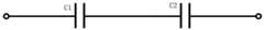
图1为本发明实施例提供的一种滤波电路的电路示意图;1 is a schematic circuit diagram of a filter circuit provided by an embodiment of the present invention;
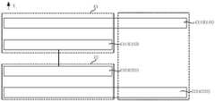
图2为本发明实施例提供的一种滤波电路的剖面结构示意图;2 is a schematic cross-sectional structural diagram of a filter circuit provided by an embodiment of the present invention;
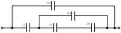
图3为图2对应的一种滤波电路的等效电路示意图;FIG. 3 is a schematic diagram of an equivalent circuit of a filter circuit corresponding to FIG. 2;
图4为现有技术提供的一种滤波电路的电路示意图;4 is a schematic circuit diagram of a filter circuit provided by the prior art;
图5为本发明实施例提供的另一种滤波电路的电路示意图;5 is a schematic circuit diagram of another filter circuit provided by an embodiment of the present invention;
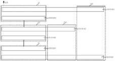
图6为本发明实施例提供的另一种滤波电路的剖面结构示意图;6 is a schematic cross-sectional structural diagram of another filter circuit provided by an embodiment of the present invention;
图7为现有技术提供的另一种滤波电路的电路示意图;7 is a schematic circuit diagram of another filter circuit provided by the prior art;
图8为本发明实施例提供的另一种滤波电路的电路示意图;8 is a schematic circuit diagram of another filter circuit provided by an embodiment of the present invention;
图9为本发明实施例提供的另一种滤波电路的电路示意图;9 is a schematic circuit diagram of another filter circuit provided by an embodiment of the present invention;
图10为图9提供的滤波电路中至少两个电感的磁场方向相同时对应的一种性能示意图;FIG. 10 is a performance schematic diagram corresponding to when the magnetic field directions of at least two inductors in the filter circuit provided in FIG. 9 are the same;
图11为图9提供的滤波电路中至少两个电感的磁场方向不同时对应的一种性能示意图;FIG. 11 is a performance schematic diagram corresponding to when the magnetic field directions of at least two inductors in the filter circuit provided in FIG. 9 are different;
图12为现有技术提供的另一种滤波电路的电路示意图;12 is a schematic circuit diagram of another filter circuit provided by the prior art;
图13为图12提供的滤波电路的一种性能示意图;Fig. 13 is a performance schematic diagram of the filter circuit provided in Fig. 12;
图14为图8提供的滤波电路的一种性能示意图;Fig. 14 is a performance schematic diagram of the filter circuit provided in Fig. 8;
图15为本发明实施例提供的一种多工器的结构示意图。FIG. 15 is a schematic structural diagram of a multiplexer according to an embodiment of the present invention.
具体实施方式Detailed ways
下面结合附图和实施例对本发明作进一步的详细说明。可以理解的是,此处所描述的具体实施例仅仅用于解释本发明,而非对本发明的限定。另外还需要说明的是,为了便于描述,附图中仅示出了与本发明相关的部分而非全部结构。The present invention will be further described in detail below in conjunction with the accompanying drawings and embodiments. It should be understood that the specific embodiments described herein are only used to explain the present invention, but not to limit the present invention. In addition, it should be noted that, for the convenience of description, the drawings only show some but not all structures related to the present invention.
图1为本发明实施例提供的一种滤波电路的电路示意图,图2为本发明实施例提供的一种滤波电路的剖面结构示意图。如图1和图2所示,该滤波电路包括至少两个串联的电容,至少两个串联的电容包括第一电容C1和第二电容C2;第一电容C1包括第一电容极板C11,第二电容C2包括第二电容极板C22;在第一方向X上,第一电容极板C11的垂直投影与第二电容极板C22的垂直投影至少部分交叠;其中,第一方向X为第一电容极板C11的厚度方向。FIG. 1 is a schematic circuit diagram of a filter circuit provided by an embodiment of the present invention, and FIG. 2 is a schematic cross-sectional structural schematic diagram of a filter circuit provided by an embodiment of the present invention. As shown in FIG. 1 and FIG. 2 , the filter circuit includes at least two capacitors connected in series, and the at least two capacitors connected in series include a first capacitor C1 and a second capacitor C2; the first capacitor C1 includes a first capacitor plate C11, and the first capacitor C1 includes a first capacitor plate C11. The second capacitor C2 includes a second capacitor plate C22; in the first direction X, the vertical projection of the first capacitor plate C11 and the vertical projection of the second capacitor plate C22 at least partially overlap; wherein, the first direction X is the first The thickness direction of a capacitor plate C11.
具体地,第一电容C1的第一端作为滤波电路的第一端,第一电容C1的第二端与第二电容C2的第一端连接,第二电容C2的第二端作为滤波电路的第二端,实现第一电容C1和第二电容C2的串联。第一电容C1和第二电容C2具有两个导电极,常见的电容导电极可以为极板。第一电容C1包括的第一电容极板C11可以划分为两个极板,两个极板之间具有介质,并在厚度方向上的垂直投影至少部分交叠,使得第一电容极板C11和介质形成第一电容C1。同理,第二电容C2包括的第二电容极板C22同样可以划分为两个极板,两个极板之间具有介质,并在厚度方向上的垂直投影至少部分交叠,使得第二电容极板C22和介质形成第二电容C2。在第一方向X上,第一电容极板C11的垂直投影与第二电容极板C22的垂直投影至少部分交叠时,使得第一电容极板C11和第二电容极板C22可以作为一个新电容的两个极板,同时第一电容极板C11和第二电容极板C22在第一方向X具有一定的空间,可以实现第一电容极板C11和第二电容极板C22之间具有介质,从而使得第一电容极板C11和第二电容极板C22以及两者之间的介质形成新的电容。示例性地,当滤波电路采用注塑工艺形成封装时,第一电容极板C11和第二电容极板C22之间的介质可以为封装层。第一电容极板C11和第二电容极板C22不同的极板部分组成新的电容时,可以使新的电容与第一电容C1和第二电容C2中的一个具有并联连接关系,或者与第一电容C1和第二电容C2同时形成π型连接。进而在不额外设置电容的基础上,增加了滤波电路中的电容数量,同时增加了滤波电路中的电容值,从而可以在不增加滤波电路占用空间的基础上提高滤波电路的性能,或者可以在保证滤波电路性能的基础上减小滤波电路的占用空间,有利于提高滤波电路的集成度。Specifically, the first end of the first capacitor C1 serves as the first end of the filter circuit, the second end of the first capacitor C1 is connected to the first end of the second capacitor C2, and the second end of the second capacitor C2 serves as the first end of the filter circuit At the second end, the first capacitor C1 and the second capacitor C2 are connected in series. The first capacitor C1 and the second capacitor C2 have two conductive electrodes, and the common conductive electrodes of capacitors can be polar plates. The first capacitor electrode plate C11 included in the first capacitor C1 can be divided into two electrode plates, and there is a medium between the two electrode plates, and the vertical projections in the thickness direction at least partially overlap, so that the first capacitor electrode plate C11 and The medium forms the first capacitor C1. Similarly, the second capacitor electrode plate C22 included in the second capacitor C2 can also be divided into two electrode plates, and there is a medium between the two electrode plates, and the vertical projections in the thickness direction at least partially overlap, so that the second capacitor The plate C22 and the dielectric form the second capacitor C2. In the first direction X, when the vertical projection of the first capacitor plate C11 and the vertical projection of the second capacitor plate C22 at least partially overlap, the first capacitor plate C11 and the second capacitor plate C22 can be used as a new The two plates of the capacitor, while the first capacitor plate C11 and the second capacitor plate C22 have a certain space in the first direction X, so that there is a medium between the first capacitor plate C11 and the second capacitor plate C22. , so that the first capacitor plate C11 and the second capacitor plate C22 and the medium between them form a new capacitor. Exemplarily, when the filter circuit is encapsulated by an injection molding process, the medium between the first capacitor plate C11 and the second capacitor plate C22 may be an encapsulation layer. When the different plate parts of the first capacitor plate C11 and the second capacitor plate C22 form a new capacitor, the new capacitor can be connected in parallel with one of the first capacitor C1 and the second capacitor C2, or with the first capacitor C1 and the second capacitor C2. A capacitor C1 and a second capacitor C2 form a π-type connection at the same time. Furthermore, on the basis of not setting additional capacitors, the number of capacitors in the filter circuit is increased, and the capacitance value in the filter circuit is also increased, so that the performance of the filter circuit can be improved without increasing the space occupied by the filter circuit, or it can be used in the filter circuit. On the basis of ensuring the performance of the filter circuit, the occupied space of the filter circuit is reduced, which is beneficial to improve the integration degree of the filter circuit.
需要说明的是,第一电容极板C11的垂直投影与第二电容极板C22的垂直投影至少部分交叠时,可以是第一电容极板C11中两个极板中的至少一个与第二电容极板C22中两个极板中的至少一个在第一方向X上的垂直投影至少部分交叠,其中,第一电容极板C11中两个极板中的至少一个与第二电容极板C22中两个极板中的至少一个不连接。It should be noted that, when the vertical projection of the first capacitor plate C11 and the vertical projection of the second capacitor plate C22 at least partially overlap, it may be at least one of the two plates in the first capacitor plate C11 and the second capacitor plate C11. The vertical projection of at least one of the two polar plates in the capacitor plate C22 in the first direction X at least partially overlaps, wherein at least one of the two polar plates in the first capacitive plate C11 and the second capacitive plate At least one of the two plates in C22 is not connected.
本实施例的技术方案,通过设置至少两个串联的电容中,第一电容的第一电容极板和第二电容的第二电容极板在第一方向上的垂直投影至少部分交叠,可以使得第一电容极板和第二电容极板形成新的电容,在不额外设置电容的基础上,增加了滤波电路中的电容数量,同时增加了滤波电路中的电容值,从而可以在不增加滤波电路占用空间的基础上提高滤波电路的性能,或者可以在保证滤波电路性能的基础上减小滤波电路的占用空间,有利于提高滤波电路的集成度。In the technical solution of this embodiment, by setting at least two capacitors connected in series, the vertical projections of the first capacitor plate of the first capacitor and the second capacitor plate of the second capacitor in the first direction at least partially overlap, so that the The first capacitor plate and the second capacitor plate form a new capacitor. On the basis of not setting additional capacitors, the number of capacitors in the filter circuit is increased, and the capacitance value in the filter circuit is also increased, so that it can be The performance of the filter circuit can be improved on the basis of the space occupied by the filter circuit, or the space occupied by the filter circuit can be reduced on the basis of ensuring the performance of the filter circuit, which is beneficial to improve the integration degree of the filter circuit.
在上述技术方案的基础上,第一电容极板和第二电容极板平行设置。On the basis of the above technical solution, the first capacitor electrode plate and the second capacitor electrode plate are arranged in parallel.
具体地,第一电容极板和第二电容极板用于形成新电容时,新电容的电容值与第一电容极板和第二电容极板之间的距离成反比。通过设置第一电容极板和第二电容极板平行设置,可以使新电容的两个极板之间的距离为定值,从而使得新电容的电容值容易计算,以便于根据滤波电路的需要设置第一电容极板和第二电容极板在第一方向上的交叠面积。Specifically, when the first capacitor plate and the second capacitor plate are used to form a new capacitor, the capacitance value of the new capacitor is inversely proportional to the distance between the first capacitor plate and the second capacitor plate. By setting the first capacitor plate and the second capacitor plate in parallel, the distance between the two plates of the new capacitor can be fixed, so that the capacitance value of the new capacitor can be easily calculated, so as to meet the needs of the filter circuit The overlapping area of the first capacitor electrode plate and the second capacitor electrode plate in the first direction is set.
在上述各技术方案的基础上,第一电容极板包括相对设置的第一电容上极板和第一电容下极板,第二电容极板包括相对设置的第二电容上极板和第二电容下极板,第一电容下极板与第二电容上极板相邻设置;第一电容上极板在第一方向上的垂直投影与第二电容上极板和第二电容下极板中的至少一个在第一方向上的垂直投影至少部分交叠,或者,第一电容下极板与第二电容下极板在第一方向上的垂直投影至少部分交叠。On the basis of the above technical solutions, the first capacitor plate includes a first capacitor upper plate and a first capacitor lower plate arranged oppositely, and the second capacitor plate includes a second capacitor upper plate and a second capacitor arranged oppositely. The lower electrode plate of the capacitor, the lower electrode plate of the first capacitor is arranged adjacent to the upper electrode plate of the second capacitor; the vertical projection of the upper electrode plate of the first capacitor in the first direction is the same as the upper electrode plate of the second capacitor and the lower electrode plate of the second capacitor. The vertical projections of at least one of them in the first direction at least partially overlap, or the vertical projections of the first capacitor lower plate and the second capacitor lower plate in the first direction at least partially overlap.
具体地,在第一电容与第二电容串联时,可以使得第一电容下极板与第二电容上极板电连接。此时第一电容下极板的电位与第二电容上极板的电位相同。在形成新电容时,可以设置第一电容上极板与第二电容上极板形成新电容,此时新电容与第一电容并联。或者可以设置第一电容上极板与第二电容下极板形成新电容,此时新电容与第一电容和第二电容形成π型连接。或者可以设置第一电容下极板与第二电容下极板形成新电容,此时新电容与第二电容并联。Specifically, when the first capacitor and the second capacitor are connected in series, the lower plate of the first capacitor can be electrically connected to the upper plate of the second capacitor. At this time, the potential of the lower plate of the first capacitor is the same as the potential of the upper plate of the second capacitor. When forming a new capacitor, the upper plate of the first capacitor and the upper plate of the second capacitor may be set to form a new capacitor, and at this time, the new capacitor is connected in parallel with the first capacitor. Alternatively, the upper plate of the first capacitor and the lower plate of the second capacitor can be set to form a new capacitor, and at this time, the new capacitor forms a π-type connection with the first capacitor and the second capacitor. Alternatively, the lower electrode plate of the first capacitor and the lower electrode plate of the second capacitor can be set to form a new capacitor, and at this time, the new capacitor is connected in parallel with the second capacitor.
优选地,继续参考图2,第一电容上极板C111在第一方向X上的垂直投影与第二电容下极板C222在第一方向X上的垂直投影至少部分交叠。Preferably, with continued reference to FIG. 2 , the vertical projection of the first capacitor upper plate C111 in the first direction X and the vertical projection of the second capacitor lower plate C222 in the first direction X at least partially overlap.
具体地,图3为图2对应的一种滤波电路的等效电路示意图。如图2和图3所示,当第一电容上极板C111在第一方向X上的垂直投影与第二电容下极板C222在第一方向X上的垂直投影至少部分交叠时,第一电容上极板C111与第二电容下极板C222形成新的电容,作为第一寄生电容Cs1。此时第一寄生电容Cs1的第一端与第一电容C1的第一端连接,第一寄生电容Cs1的第二端与第二电容C2的第二端连接,实现了第一寄生电容Cs1、第一电容C1和第二电容C2形成π型连接。Specifically, FIG. 3 is a schematic diagram of an equivalent circuit of a filter circuit corresponding to FIG. 2 . As shown in FIG. 2 and FIG. 3 , when the vertical projection of the first capacitor upper plate C111 in the first direction X and the vertical projection of the second capacitor lower plate C222 in the first direction X at least partially overlap, the A capacitor upper plate C111 and a second capacitor lower plate C222 form a new capacitor as the first parasitic capacitor Cs1. At this time, the first end of the first parasitic capacitor Cs1 is connected to the first end of the first capacitor C1, and the second end of the first parasitic capacitor Cs1 is connected to the second end of the second capacitor C2, so that the first parasitic capacitor Cs1, The first capacitor C1 and the second capacitor C2 form a π-type connection.
图4为现有技术提供的一种滤波电路的电路示意图。如图4所示,现有的滤波电路可以包括T型连接的三个电容,分别为第一T型电容C01、第二T型电容C02和第三T型电容C03。第一T型电容C01和第二T型电容C02串联,第三T型电容C03的一端连接至第一T型电容C01和第二T型电容C02的连接点。此时滤波电路需要设置三个电容。在此基础上,参考图2和图3,通过设置滤波电路包括第一电容C1和第二电容C2,第一电容上极板C111在第一方向X上的垂直投影与第二电容下极板C222在第一方向X上的垂直投影至少部分交叠,使得第一寄生电容Cs1、第一电容C1和第二电容C2形成π型连接,不仅可以在保持滤波电路性能的基础上减少电容的数量设置,减少了滤波电路的占用空间。同时可以将电容的T型连接转换为π型连接,在保持滤波电路的等效容值不变的基础上,可以减小第一电容和第二电容的容值需求,从而可以进一步地减小滤波电路的占用空间。FIG. 4 is a schematic circuit diagram of a filter circuit provided in the prior art. As shown in FIG. 4 , the existing filter circuit may include three capacitors connected in a T-type connection, namely a first T-type capacitor C01 , a second T-type capacitor C02 and a third T-type capacitor C03 . The first T-type capacitor C01 and the second T-type capacitor C02 are connected in series, and one end of the third T-type capacitor C03 is connected to the connection point of the first T-type capacitor C01 and the second T-type capacitor C02. At this time, the filter circuit needs to set three capacitors. On this basis, referring to FIG. 2 and FIG. 3 , by setting the filter circuit to include a first capacitor C1 and a second capacitor C2, the vertical projection of the upper plate C111 of the first capacitor in the first direction X is the same as the lower plate of the second capacitor. The vertical projections of C222 in the first direction X at least partially overlap, so that the first parasitic capacitor Cs1, the first capacitor C1 and the second capacitor C2 form a π-type connection, which can not only reduce the number of capacitors on the basis of maintaining the performance of the filter circuit set, reducing the space occupied by the filter circuit. At the same time, the T-type connection of the capacitor can be converted into a π-type connection. On the basis of keeping the equivalent capacitance of the filter circuit unchanged, the capacitance requirements of the first capacitor and the second capacitor can be reduced, thereby further reducing The space occupied by the filter circuit.
可选地,继续参考图2,第一电容上极板C111在第一方向X上的垂直投影与第二电容下极板C222在第一方向X上的垂直投影完全交叠。Optionally, with continued reference to FIG. 2 , the vertical projection of the first capacitor upper plate C111 in the first direction X completely overlaps the vertical projection of the second capacitor lower plate C222 in the first direction X.
具体地,电容的两个极板在厚度方向的垂直投影交叠的面积与电容值成正比。第一寄生电容Cs1的两个极板为第一电容上极板C111和第二电容下极板C222。通过设置第一电容上极板C111在第一方向X上的垂直投影与第二电容下极板C222在第一方向X上的垂直投影完全交叠,可以使得第一寄生电容Cs1的两个极板在厚度方向的垂直投影交叠的面积最大,从而有利于实现第一寄生电容Cs1具有较大的容值,有利于提高滤波电路的性能。Specifically, the overlapping area of the vertical projections of the two polar plates of the capacitor in the thickness direction is proportional to the capacitance value. The two plates of the first parasitic capacitor Cs1 are the first capacitor upper plate C111 and the second capacitor lower plate C222. By setting the vertical projection of the first capacitor upper plate C111 in the first direction X and the vertical projection of the second capacitor lower plate C222 in the first direction X to completely overlap, the two poles of the first parasitic capacitor Cs1 can be made to overlap. The overlapping area of the vertical projections of the plates in the thickness direction is the largest, which is beneficial to realize that the first parasitic capacitance Cs1 has a larger capacitance value and is beneficial to improve the performance of the filter circuit.
图5为本发明实施例提供的另一种滤波电路的电路示意图,图6为本发明实施例提供的另一种滤波电路的剖面结构示意图。如图5和图6所示,该滤波电路还包括第三电容C3,第三电容C3串联于第一电容C1远离第二电容C2的一端;第三电容C3包括第三电容极板C33;在第二方向Y上,第三电容极板C33的垂直投影与第二电容极板C22的垂直投影至少部分交叠;其中,第二方向Y为第二电容极板C22的厚度方向。FIG. 5 is a schematic circuit diagram of another filter circuit provided by an embodiment of the present invention, and FIG. 6 is a schematic cross-sectional structure diagram of another filter circuit provided by an embodiment of the present invention. As shown in FIG. 5 and FIG. 6 , the filter circuit further includes a third capacitor C3, which is connected in series with one end of the first capacitor C1 away from the second capacitor C2; the third capacitor C3 includes a third capacitor plate C33; In the second direction Y, the vertical projection of the third capacitor plate C33 and the vertical projection of the second capacitor plate C22 at least partially overlap; wherein the second direction Y is the thickness direction of the second capacitor plate C22.
具体地,第三电容C3串联于第一电容C1和第二电容C2的一侧,实现第三电容C3、第一电容C1和第二电容C2的串联。示例性地,如图5所示,第三电容C3可以串联于第一电容C1远离第二电容C2的一端。第二方向Y为第二电容极板C22的厚度方向,第一方向X为第一电容极板C11的厚度方向,当第一电容极板C11和第二电容极板C22平行时,第二方向Y与第一方向X为相同的方向。第三电容极板C33可以划分为两个极板,两个极板之间具有介质,并在厚度方向上的垂直投影至少部分交叠,使得第三电容极板C33和介质形成第三电容C3。在第二方向Y上,第三电容极板C33的垂直投影与第二电容极板C22的垂直投影至少部分交叠时,使得第三电容极板C33和第二电容极板C22可以作为另一个新的电容的两个极板,同时第三电容极板C33和第二电容极板C22在第二方向Y上具有一定的空间,可以实现第三电容极板C33和第二电容极板C22之间具有介质。示例性地,当滤波电路采用注塑工艺形成封装时,第三电容极板C33和第二电容极板C22之间的介质可以为封装层。从而使得第三电容极板C33和第二电容极板C22以及两者之间的介质形成另一个新的电容。进而在不额外设置电容的基础上,增加了滤波电路中的电容数量,同时增加了滤波电路中的电容值,从而可以在不增加滤波电路占用空间的基础上提高滤波电路的性能,或者可以在保证滤波电路性能的基础上减小滤波电路的占用空间,有利于提高滤波电路的集成度。Specifically, the third capacitor C3 is connected in series with one side of the first capacitor C1 and the second capacitor C2 to realize the series connection of the third capacitor C3, the first capacitor C1 and the second capacitor C2. Exemplarily, as shown in FIG. 5 , the third capacitor C3 may be connected in series with one end of the first capacitor C1 away from the second capacitor C2 . The second direction Y is the thickness direction of the second capacitor plate C22, and the first direction X is the thickness direction of the first capacitor plate C11. When the first capacitor plate C11 and the second capacitor plate C22 are parallel, the second direction Y and the first direction X are the same direction. The third capacitor electrode plate C33 can be divided into two electrode plates, and there is a medium between the two electrode plates, and the vertical projections in the thickness direction at least partially overlap, so that the third capacitor electrode plate C33 and the medium form a third capacitor C3 . In the second direction Y, when the vertical projection of the third capacitor plate C33 and the vertical projection of the second capacitor plate C22 at least partially overlap, so that the third capacitor plate C33 and the second capacitor plate C22 can serve as another The two plates of the new capacitor, while the third capacitor plate C33 and the second capacitor plate C22 have a certain space in the second direction Y, which can realize the difference between the third capacitor plate C33 and the second capacitor plate C22. There is a medium in between. Exemplarily, when the filter circuit is encapsulated by an injection molding process, the medium between the third capacitor plate C33 and the second capacitor plate C22 may be an encapsulation layer. Thus, the third capacitor plate C33 and the second capacitor plate C22 and the medium between them form another new capacitor. Furthermore, on the basis of not setting additional capacitors, the number of capacitors in the filter circuit is increased, and the capacitance value in the filter circuit is also increased, so that the performance of the filter circuit can be improved without increasing the space occupied by the filter circuit, or it can be used in the filter circuit. On the basis of ensuring the performance of the filter circuit, the occupied space of the filter circuit is reduced, which is beneficial to improve the integration degree of the filter circuit.
示例性地,第三电容极板C33可以包括相对设置的第三电容上极板C331和第三电容下极板C332,第一电容极板C11可以包括相对设置的第一电容上极板C111和第一电容下极板C112,第二电容极板C22可以包括相对设置的第二电容上极板C221和第二电容下极板C222。第三电容下极板C332可以与第一电容上极板C111连接,第一电容下极板C112与第二电容上极板C221连接,实现第一电容C1、第二电容C2和第三电容C3的串联。此时可以设置第三电容上极板C331和第二电容下极板C222在第二方向Y上的垂直投影至少部分交叠,并形成另一个新的电容,作为第二寄生电容Cs2。此时第二寄生电容Cs2的第一端与第三电容上极板C331连接,第二寄生电容Cs2的第二端与第二电容下极板C222连接,实现了第二寄生电容Cs2、第三电容C3和第二电容C2的等效π型连接。Exemplarily, the third capacitor plate C33 may include a third capacitor upper plate C331 and a third capacitor lower plate C332 arranged oppositely, and the first capacitor plate C11 may include a relatively arranged first capacitor upper plate C111 and The first capacitor lower electrode plate C112 and the second capacitor electrode plate C22 may include a second capacitor upper electrode plate C221 and a second capacitor lower electrode plate C222 which are disposed opposite to each other. The third capacitor lower plate C332 can be connected to the first capacitor upper plate C111, and the first capacitor lower plate C112 is connected to the second capacitor upper plate C221 to realize the first capacitor C1, the second capacitor C2 and the third capacitor C3 of concatenation. At this time, the vertical projections of the third capacitor upper plate C331 and the second capacitor lower plate C222 in the second direction Y may at least partially overlap to form another new capacitor as the second parasitic capacitor Cs2. At this time, the first end of the second parasitic capacitor Cs2 is connected to the upper plate C331 of the third capacitor, and the second end of the second parasitic capacitor Cs2 is connected to the lower plate C222 of the second capacitor, thereby realizing the second parasitic capacitance Cs2, the third Equivalent π-type connection of the capacitor C3 and the second capacitor C2.
图7为现有技术提供的另一种滤波电路的电路示意图。如图7所示,现有的滤波电路可以包括双T型连接的五个电容,即在图4的基础上,增加了第四T型电容C04和第五T型电容C05。第四T型电容C04与第一T型电容C01和第二T型电容C02串联,第五T型电容C05的一端连接至第四T型电容C04和第一T型电容C01的连接点。此时滤波电路需要设置五个电容。在此基础上,参考图5和图6,通过设置滤波电路包括第一电容C1、第二电容C2和第三电容C3,在第一方向X上,第一电容上极板C111的垂直投影与第二电容下极板C222的垂直投影至少部分交叠,在第二方向Y上,第三电容极板C33的垂直投影与第二电容极板C22的垂直投影至少部分交叠,从而可以形成第一寄生电容Cs1和第二寄生电容Cs2,不仅可以在保持滤波电路性能的基础上减少电容的数量设置,减少了滤波电路的占用空间。同时可以将电容的T型连接转换为π型连接,在保持滤波电路的等效容值不变的基础上,可以减小第一电容和第二电容的容值需求,从而可以进一步地减小滤波电路的占用空间。FIG. 7 is a schematic circuit diagram of another filter circuit provided in the prior art. As shown in FIG. 7 , the existing filter circuit may include five capacitors connected with double T-types, that is, on the basis of FIG. 4 , a fourth T-type capacitor C04 and a fifth T-type capacitor C05 are added. The fourth T-type capacitor C04 is connected in series with the first T-type capacitor C01 and the second T-type capacitor C02, and one end of the fifth T-type capacitor C05 is connected to the connection point of the fourth T-type capacitor C04 and the first T-type capacitor C01. At this time, the filter circuit needs to set five capacitors. On this basis, referring to FIG. 5 and FIG. 6 , by setting the filter circuit to include the first capacitor C1, the second capacitor C2 and the third capacitor C3, in the first direction X, the vertical projection of the upper plate C111 of the first capacitor is the same as the The vertical projection of the second capacitor lower plate C222 at least partially overlaps, and in the second direction Y, the vertical projection of the third capacitor plate C33 and the vertical projection of the second capacitor plate C22 at least partially overlap, thereby forming a first The first parasitic capacitor Cs1 and the second parasitic capacitor Cs2 can not only reduce the number of capacitors on the basis of maintaining the performance of the filter circuit, but also reduce the space occupied by the filter circuit. At the same time, the T-type connection of the capacitor can be converted into a π-type connection. On the basis of keeping the equivalent capacitance of the filter circuit unchanged, the capacitance requirements of the first capacitor and the second capacitor can be reduced, thereby further reducing The space occupied by the filter circuit.
优选地,参考图6,第三电容极板C33在第二方向Y上的垂直投影与第二电容极板C22在第二方向Y上的垂直投影完全交叠,可以使得第二寄生电容Cs2的两个极板在厚度方向的垂直投影交叠的面积最大,从而有利于实现第一寄生电容Cs1具有较大的容值,有利于提高滤波电路的性能。Preferably, referring to FIG. 6 , the vertical projection of the third capacitor plate C33 in the second direction Y completely overlaps the vertical projection of the second capacitor plate C22 in the second direction Y, which can make the second parasitic capacitance Cs2 The overlapping area of the vertical projections of the two polar plates in the thickness direction is the largest, which is beneficial to realize that the first parasitic capacitor Cs1 has a larger capacitance value and is beneficial to improve the performance of the filter circuit.
在上述技术方案的基础上,第三电容极板和第二电容极板平行设置。On the basis of the above technical solution, the third capacitor electrode plate and the second capacitor electrode plate are arranged in parallel.
具体地,第三电容极板和第二电容极板用于形成新电容时,新电容的电容值与第三电容极板和第二电容极板之间的距离成反比。通过设置第三电容极板和第二电容极板平行设置,可以使新电容的两个极板之间的距离为定值,从而使得新电容的电容值容易计算,以便于根据滤波电路的需要设置第三电容极板和第二电容极板在第二方向上的交叠面积。Specifically, when the third capacitor electrode plate and the second capacitor electrode plate are used to form a new capacitor, the capacitance value of the new capacitor is inversely proportional to the distance between the third capacitor electrode plate and the second capacitor electrode plate. By setting the third capacitor pole plate and the second capacitor pole plate in parallel, the distance between the two pole plates of the new capacitor can be fixed, so that the capacitance value of the new capacitor can be easily calculated, so as to meet the needs of the filter circuit The overlapping area of the third capacitor electrode plate and the second capacitor electrode plate in the second direction is set.
图8为本发明实施例提供的另一种滤波电路的电路示意图。如图8所示,滤波电路还包括至少两个电感L,至少两个电感L的一端与电容的连接点连接,至少两个电感L的磁场方向相同;其中,电容的连接点为串联电容之间的连接点。FIG. 8 is a schematic circuit diagram of another filter circuit provided by an embodiment of the present invention. As shown in FIG. 8 , the filter circuit further includes at least two inductors L, one end of the at least two inductors L is connected to the connection point of the capacitor, and the magnetic field directions of the at least two inductors L are the same; wherein, the connection point of the capacitor is the connection point between the series capacitors. connection point between.
具体地,电容包括串联的至少两个电容,电容的连接点为串联电容之间的连接点。示例性地,如图8所示,电容包括串联的第一电容C1、第二电容C2和第三电容C3。此时电容的连接点包括第一电容C1与第二电容C2的连接点N1以及第三电容C3与第一电容C1的连接点N2。滤波电路包括两个电感L,每个电感L的一端分别与一个电容的连接点连接。示例性地,如图8所示,一个电感L的一端与第一电容C1与第二电容C2的连接点N1连接,另一个电感L的一端与第三电容C3与第一电容C1的连接点N2连接。通过设置至少两个电感L的磁场方向相同,可以使得至少两个电感L之间具有正耦合,从而可以形成一个传输零点,有利于提高滤波电路的滤波性能。Specifically, the capacitor includes at least two capacitors connected in series, and the connection point of the capacitors is the connection point between the capacitors in series. Exemplarily, as shown in FIG. 8 , the capacitor includes a first capacitor C1 , a second capacitor C2 and a third capacitor C3 connected in series. At this time, the connection points of the capacitors include the connection point N1 of the first capacitor C1 and the second capacitor C2 and the connection point N2 of the third capacitor C3 and the first capacitor C1. The filter circuit includes two inductors L, and one end of each inductor L is respectively connected to a connection point of a capacitor. Exemplarily, as shown in FIG. 8, one end of one inductor L is connected to the connection point N1 of the first capacitor C1 and the second capacitor C2, and one end of the other inductor L is connected to the connection point of the third capacitor C3 and the first capacitor C1. N2 connection. By setting the magnetic field directions of the at least two inductors L to be the same, positive coupling can be formed between the at least two inductors L, so that a transmission zero point can be formed, which is beneficial to improve the filtering performance of the filtering circuit.
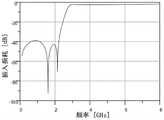
示例性地,图9为本发明实施例提供的另一种滤波电路的电路示意图,图10为图9提供的滤波电路中至少两个电感的磁场方向相同时对应的一种性能示意图,图11为图9提供的滤波电路中至少两个电感的磁场方向不同时对应的一种性能示意图。其中,横坐标为频率,纵坐标为插入损耗。由图10和图11可知,通过设置至少两个电感L的磁场方向相同,至少两个电感L之间具有正耦合,从而可以在滤波电路的通带频率范围外形成传输零点,从而可以提高滤波电路的抑制效果,有效地提高了滤波电路的滤波效果。Exemplarily, FIG. 9 is a schematic circuit diagram of another filter circuit provided by an embodiment of the present invention, FIG. 10 is a schematic diagram of a performance corresponding to at least two inductors in the filter circuit provided in FIG. 9 when the magnetic field directions of at least two inductors are the same, and FIG. 11 . A performance schematic diagram corresponding to when the magnetic field directions of at least two inductors in the filter circuit of FIG. 9 are different. Among them, the abscissa is the frequency, and the ordinate is the insertion loss. It can be seen from Fig. 10 and Fig. 11 that by setting at least two inductors L with the same magnetic field direction and positive coupling between at least two inductors L, a transmission zero point can be formed outside the passband frequency range of the filter circuit, so that the filter can be improved. The suppression effect of the circuit effectively improves the filtering effect of the filter circuit.
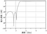
在此基础上,图12为现有技术提供的另一种滤波电路的电路示意图,图13为图12提供的滤波电路的一种性能示意图。其中,横坐标为频率,纵坐标为插入损耗。如图12所示,滤波电路在具有双T型连接的五个电容的基础上,还包括两个滤波电感L’,两个滤波电感L’分别串联在第五T型电容C05的一端与第四T型电容C04和第一T型电容C01的连接点之间,以及第三T型电容C03的一端与第一T型电容C01和第二T型电容C02的连接点之间。如图13所示,滤波电路在通带频率范围外具有两个传输零点。On this basis, FIG. 12 is a schematic circuit diagram of another filter circuit provided in the prior art, and FIG. 13 is a performance schematic diagram of the filter circuit provided in FIG. 12 . Among them, the abscissa is the frequency, and the ordinate is the insertion loss. As shown in Figure 12, the filter circuit further includes two filter inductors L' on the basis of the five capacitors with double T-type connections. The two filter inductors L' are respectively connected in series with one end of the fifth T-type capacitor C05 and the first Between the connection point of the four T-type capacitors C04 and the first T-type capacitor C01, and between one end of the third T-type capacitor C03 and the connection point of the first T-type capacitor C01 and the second T-type capacitor C02. As shown in Figure 13, the filter circuit has two transmission zeros outside the passband frequency range.
图14为图8提供的滤波电路的一种性能示意图。其中,横坐标为频率,纵坐标为插入损耗。继续参考图8和图14,当第一电容C1和第二电容C2之间具有第一寄生电容Cs1,第三电容C3和第二电容C2之间具有第一寄生电容Cs2,且至少两个电感L的磁场方向相同时,滤波电路同样在通带频率范围外具有两个传输零点。由此可知,在第一电容C1和第二电容C2之间具有第一寄生电容Cs1,第三电容C3和第二电容C2之间具有第一寄生电容Cs2,且至少两个电感L的磁场方向相同时,滤波电路可以在不减少传输零点的同时减少电容的数量,减少了滤波电路的占用空间。同时可以在保持滤波电路的等效容值不变的基础上减小电容所需的电容值,从而可以进一步地减小滤波电路的占用空间。FIG. 14 is a performance diagram of the filter circuit provided in FIG. 8 . Among them, the abscissa is the frequency, and the ordinate is the insertion loss. Continuing to refer to FIG. 8 and FIG. 14 , when there is a first parasitic capacitance Cs1 between the first capacitor C1 and the second capacitor C2, a first parasitic capacitance Cs2 between the third capacitor C3 and the second capacitor C2, and at least two inductances When the magnetic field direction of L is the same, the filter circuit also has two transmission zeros outside the passband frequency range. It can be seen from this that there is a first parasitic capacitance Cs1 between the first capacitor C1 and the second capacitor C2, a first parasitic capacitance Cs2 between the third capacitor C3 and the second capacitor C2, and the magnetic field directions of the at least two inductors L At the same time, the filter circuit can reduce the number of capacitors without reducing the transmission zero point, thereby reducing the occupied space of the filter circuit. At the same time, the capacitance value required by the capacitor can be reduced on the basis of keeping the equivalent capacitance value of the filter circuit unchanged, thereby further reducing the occupied space of the filter circuit.
本发明实施例还提供一种滤波器。该滤波器包括本发明任意实施例提供的滤波电路。The embodiment of the present invention also provides a filter. The filter includes the filter circuit provided by any embodiment of the present invention.
具体地,滤波器至少包括本发明任意实施例提供的滤波电路,因此具有滤波电路的有益效果,此处不再赘述。另外,滤波器还可以包括其他滤波电路,用于提高滤波器的滤波功能。示例性地,其他滤波电路可以是低通滤波电路、高通滤波电路或带通滤波电路,本发明实施例不做限定。Specifically, the filter includes at least the filter circuit provided in any embodiment of the present invention, and thus has the beneficial effect of the filter circuit, which will not be repeated here. In addition, the filter may also include other filtering circuits for improving the filtering function of the filter. Exemplarily, the other filter circuit may be a low-pass filter circuit, a high-pass filter circuit, or a band-pass filter circuit, which is not limited in this embodiment of the present invention.
本发明实施例还提供一种多工器。图15为本发明实施例提供的一种多工器的结构示意图。如图15所示,该多工器包括本发明任意实施例提供的滤波电路210。The embodiment of the present invention also provides a multiplexer. FIG. 15 is a schematic structural diagram of a multiplexer according to an embodiment of the present invention. As shown in FIG. 15 , the multiplexer includes the
继续参考图15,多工器包括一个第一端IN和至少两个第二端;每一滤波电路210串联连接于多工器的第一端IN和任一第二端之间。Continuing to refer to FIG. 15 , the multiplexer includes a first terminal IN and at least two second terminals; each
具体地,图15中示例性地示出了多工器包括一个第一端IN和n个第二端,分别为OUT1、OUT2……OUTn。每个滤波电路210串联于第一端IN和一第二端之间。例如,第一个滤波电路210串联于第一端IN和第一个第二端OUT1之间,第二个滤波电路210串联于第一端IN和第一个第二端OUT2之间……以此类推。由于多工器具有本发明任意实施例提供的滤波电路210,因此具有滤波电路的有益效果,此处不再赘述。Specifically, FIG. 15 exemplarily shows that the multiplexer includes one first terminal IN and n second terminals, which are OUT1 , OUT2 . . . OUTn respectively. Each
需要说明的是,多工器还可以包括其他滤波电路,其他滤波电路串联于第一端IN和任一第二端之间,其他滤波电路可以是低通滤波电路、高通滤波电路或带通滤波电路,本发明实施例不做限定。It should be noted that the multiplexer may also include other filter circuits, and the other filter circuits are connected in series between the first terminal IN and any second terminal, and the other filter circuits may be low-pass filter circuits, high-pass filter circuits or band-pass filter circuits. circuit, which is not limited in the embodiment of the present invention.
注意,上述仅为本发明的较佳实施例及所运用技术原理。本领域技术人员会理解,本发明不限于这里所述的特定实施例,对本领域技术人员来说能够进行各种明显的变化、重新调整和替代而不会脱离本发明的保护范围。因此,虽然通过以上实施例对本发明进行了较为详细的说明,但是本发明不仅仅限于以上实施例,在不脱离本发明构思的情况下,还可以包括更多其他等效实施例,而本发明的范围由所附的权利要求范围决定。Note that the above are only preferred embodiments of the present invention and applied technical principles. Those skilled in the art will understand that the present invention is not limited to the specific embodiments described herein, and various obvious changes, readjustments and substitutions can be made by those skilled in the art without departing from the protection scope of the present invention. Therefore, although the present invention has been described in detail through the above embodiments, the present invention is not limited to the above embodiments, and can also include more other equivalent embodiments without departing from the concept of the present invention. The scope is determined by the scope of the appended claims.
Claims (10)
Translated fromChinesePriority Applications (2)
| Application Number | Priority Date | Filing Date | Title |
|---|---|---|---|
| CN202210220194.0ACN114584093A (en) | 2022-03-08 | 2022-03-08 | Filter circuit, filter and multiplexer |
| PCT/CN2022/137885WO2023169025A1 (en) | 2022-03-08 | 2022-12-09 | Filter circuit, filter and multiplexer |
Applications Claiming Priority (1)
| Application Number | Priority Date | Filing Date | Title |
|---|---|---|---|
| CN202210220194.0ACN114584093A (en) | 2022-03-08 | 2022-03-08 | Filter circuit, filter and multiplexer |
Publications (1)
| Publication Number | Publication Date |
|---|---|
| CN114584093Atrue CN114584093A (en) | 2022-06-03 |
Family
ID=81774452
Family Applications (1)
| Application Number | Title | Priority Date | Filing Date |
|---|---|---|---|
| CN202210220194.0APendingCN114584093A (en) | 2022-03-08 | 2022-03-08 | Filter circuit, filter and multiplexer |
Country Status (2)
| Country | Link |
|---|---|
| CN (1) | CN114584093A (en) |
| WO (1) | WO2023169025A1 (en) |
Cited By (1)
| Publication number | Priority date | Publication date | Assignee | Title |
|---|---|---|---|---|
| WO2023169025A1 (en)* | 2022-03-08 | 2023-09-14 | 安徽安努奇科技有限公司 | Filter circuit, filter and multiplexer |
Citations (6)
| Publication number | Priority date | Publication date | Assignee | Title |
|---|---|---|---|---|
| US20030076199A1 (en)* | 2001-10-18 | 2003-04-24 | Murata Manufacturing Co., Ltd. | LC high-pass filter circuit device, laminated LC high-pass filter device, multiplexer, and radio communication apparatus |
| US20150303890A1 (en)* | 2013-10-24 | 2015-10-22 | Murata Manufacturing Co., Ltd. | Composite lc resonator and band pass filter |
| CN108011605A (en)* | 2017-12-06 | 2018-05-08 | 深圳振华富电子有限公司 | One kind miniaturization is high to suppress LTCC bandpass filters |
| US20190200454A1 (en)* | 2017-12-21 | 2019-06-27 | Qualcomm Incorporated | Three dimensional inductor-capacitor apparatus and method of fabricating |
| CN112671366A (en)* | 2021-01-20 | 2021-04-16 | 安徽安努奇科技有限公司 | Filter circuits, filters and multiplexers |
| CN113410053A (en)* | 2021-06-18 | 2021-09-17 | 安徽安努奇科技有限公司 | Capacitor |
Family Cites Families (5)
| Publication number | Priority date | Publication date | Assignee | Title |
|---|---|---|---|---|
| JP6319758B2 (en)* | 2013-02-28 | 2018-05-09 | デクセリアルズ株式会社 | Capacitance device, resonance circuit, and electronic equipment |
| KR20170109782A (en)* | 2016-03-22 | 2017-10-10 | 삼성전기주식회사 | Complex electronic component |
| CN105719613B (en)* | 2016-04-22 | 2018-06-01 | 上海天马微电子有限公司 | array substrate, display panel and display device |
| CN108512520B (en)* | 2018-02-27 | 2022-04-29 | 苏州汉天下电子有限公司 | Monolithic integrated structure of bulk acoustic wave resonator and capacitor, manufacturing method thereof, filter, duplexer, and radio frequency communication module |
| CN114584093A (en)* | 2022-03-08 | 2022-06-03 | 安徽安努奇科技有限公司 | Filter circuit, filter and multiplexer |
- 2022
- 2022-03-08CNCN202210220194.0Apatent/CN114584093A/enactivePending
- 2022-12-09WOPCT/CN2022/137885patent/WO2023169025A1/ennot_activeCeased
Patent Citations (6)
| Publication number | Priority date | Publication date | Assignee | Title |
|---|---|---|---|---|
| US20030076199A1 (en)* | 2001-10-18 | 2003-04-24 | Murata Manufacturing Co., Ltd. | LC high-pass filter circuit device, laminated LC high-pass filter device, multiplexer, and radio communication apparatus |
| US20150303890A1 (en)* | 2013-10-24 | 2015-10-22 | Murata Manufacturing Co., Ltd. | Composite lc resonator and band pass filter |
| CN108011605A (en)* | 2017-12-06 | 2018-05-08 | 深圳振华富电子有限公司 | One kind miniaturization is high to suppress LTCC bandpass filters |
| US20190200454A1 (en)* | 2017-12-21 | 2019-06-27 | Qualcomm Incorporated | Three dimensional inductor-capacitor apparatus and method of fabricating |
| CN112671366A (en)* | 2021-01-20 | 2021-04-16 | 安徽安努奇科技有限公司 | Filter circuits, filters and multiplexers |
| CN113410053A (en)* | 2021-06-18 | 2021-09-17 | 安徽安努奇科技有限公司 | Capacitor |
Cited By (1)
| Publication number | Priority date | Publication date | Assignee | Title |
|---|---|---|---|---|
| WO2023169025A1 (en)* | 2022-03-08 | 2023-09-14 | 安徽安努奇科技有限公司 | Filter circuit, filter and multiplexer |
Also Published As
| Publication number | Publication date |
|---|---|
| WO2023169025A1 (en) | 2023-09-14 |
Similar Documents
| Publication | Publication Date | Title |
|---|---|---|
| US10944375B2 (en) | Multilayer band pass filter | |
| CN102790599B (en) | Filter | |
| WO2023179089A1 (en) | Resonator, filter, and multiplexer | |
| CN110994087B (en) | A high-low-pass parallel LTCC band-stop filter | |
| CN114679149B (en) | An N77 bandpass filter based on IPD technology | |
| JP2005341577A (en) | Balun transformer and low-pass filter | |
| TWI738580B (en) | Even-mode resonator filter with high stability | |
| CN114584093A (en) | Filter circuit, filter and multiplexer | |
| JP2015089097A (en) | Polarized low pass filter and diplexer | |
| US8860531B2 (en) | Filter having electrical circuit arrangement with concentrated elements in multi-layer substrates | |
| JP2822825B2 (en) | Composite electronic components | |
| TWI736444B (en) | Coupled resonator filter with high quality factor | |
| CN112671366A (en) | Filter circuits, filters and multiplexers | |
| US7782157B2 (en) | Resonant circuit, filter circuit, and multilayered substrate | |
| JP3135443B2 (en) | Multilayer ceramic capacitors | |
| JPWO2017110179A1 (en) | Circuit board, filter circuit and capacitance element | |
| CN214429521U (en) | Filter circuit, filter and multiplexer | |
| JPH04284606A (en) | Filter element | |
| JP3197249B2 (en) | Multilayer LC high-pass filter | |
| JP3207413U (en) | Low-pass filter with stopband noise suppression | |
| JP4339819B2 (en) | High pass filter | |
| CN216981874U (en) | Filter circuit and multiplexer | |
| US20230282953A1 (en) | Multilayered filter device | |
| US12401108B2 (en) | Filter circuit | |
| CN114257202A (en) | Filter circuit and multiplexer |
Legal Events
| Date | Code | Title | Description |
|---|---|---|---|
| PB01 | Publication | ||
| PB01 | Publication | ||
| SE01 | Entry into force of request for substantive examination | ||
| SE01 | Entry into force of request for substantive examination |