CN114583482A - electrical connector assembly - Google Patents
electrical connector assemblyDownload PDFInfo
- Publication number
- CN114583482A CN114583482ACN202210276044.1ACN202210276044ACN114583482ACN 114583482 ACN114583482 ACN 114583482ACN 202210276044 ACN202210276044 ACN 202210276044ACN 114583482 ACN114583482 ACN 114583482A
- Authority
- CN
- China
- Prior art keywords
- connector assembly
- connector
- housing
- wafer
- terminals
- Prior art date
- Legal status (The legal status is an assumption and is not a legal conclusion. Google has not performed a legal analysis and makes no representation as to the accuracy of the status listed.)
- Granted
Links
Images


Classifications
- H—ELECTRICITY
- H01—ELECTRIC ELEMENTS
- H01R—ELECTRICALLY-CONDUCTIVE CONNECTIONS; STRUCTURAL ASSOCIATIONS OF A PLURALITY OF MUTUALLY-INSULATED ELECTRICAL CONNECTING ELEMENTS; COUPLING DEVICES; CURRENT COLLECTORS
- H01R12/00—Structural associations of a plurality of mutually-insulated electrical connecting elements, specially adapted for printed circuits, e.g. printed circuit boards [PCB], flat or ribbon cables, or like generally planar structures, e.g. terminal strips, terminal blocks; Coupling devices specially adapted for printed circuits, flat or ribbon cables, or like generally planar structures; Terminals specially adapted for contact with, or insertion into, printed circuits, flat or ribbon cables, or like generally planar structures
- H01R12/70—Coupling devices
- H01R12/71—Coupling devices for rigid printing circuits or like structures
- H01R12/72—Coupling devices for rigid printing circuits or like structures coupling with the edge of the rigid printed circuits or like structures
- H01R12/73—Coupling devices for rigid printing circuits or like structures coupling with the edge of the rigid printed circuits or like structures connecting to other rigid printed circuits or like structures
- H01R12/735—Printed circuits including an angle between each other
- H01R12/737—Printed circuits being substantially perpendicular to each other
- H—ELECTRICITY
- H01—ELECTRIC ELEMENTS
- H01R—ELECTRICALLY-CONDUCTIVE CONNECTIONS; STRUCTURAL ASSOCIATIONS OF A PLURALITY OF MUTUALLY-INSULATED ELECTRICAL CONNECTING ELEMENTS; COUPLING DEVICES; CURRENT COLLECTORS
- H01R13/00—Details of coupling devices of the kinds covered by groups H01R12/70 or H01R24/00 - H01R33/00
- H01R13/648—Protective earth or shield arrangements on coupling devices, e.g. anti-static shielding
- H01R13/658—High frequency shielding arrangements, e.g. against EMI [Electro-Magnetic Interference] or EMP [Electro-Magnetic Pulse]
- H01R13/6581—Shield structure
- H01R13/6585—Shielding material individually surrounding or interposed between mutually spaced contacts
- H01R13/6586—Shielding material individually surrounding or interposed between mutually spaced contacts for separating multiple connector modules
- H01R13/6587—Shielding material individually surrounding or interposed between mutually spaced contacts for separating multiple connector modules for mounting on PCBs
- H—ELECTRICITY
- H01—ELECTRIC ELEMENTS
- H01R—ELECTRICALLY-CONDUCTIVE CONNECTIONS; STRUCTURAL ASSOCIATIONS OF A PLURALITY OF MUTUALLY-INSULATED ELECTRICAL CONNECTING ELEMENTS; COUPLING DEVICES; CURRENT COLLECTORS
- H01R12/00—Structural associations of a plurality of mutually-insulated electrical connecting elements, specially adapted for printed circuits, e.g. printed circuit boards [PCB], flat or ribbon cables, or like generally planar structures, e.g. terminal strips, terminal blocks; Coupling devices specially adapted for printed circuits, flat or ribbon cables, or like generally planar structures; Terminals specially adapted for contact with, or insertion into, printed circuits, flat or ribbon cables, or like generally planar structures
- H01R12/70—Coupling devices
- H01R12/7082—Coupling device supported only by cooperation with PCB
- H—ELECTRICITY
- H01—ELECTRIC ELEMENTS
- H01R—ELECTRICALLY-CONDUCTIVE CONNECTIONS; STRUCTURAL ASSOCIATIONS OF A PLURALITY OF MUTUALLY-INSULATED ELECTRICAL CONNECTING ELEMENTS; COUPLING DEVICES; CURRENT COLLECTORS
- H01R12/00—Structural associations of a plurality of mutually-insulated electrical connecting elements, specially adapted for printed circuits, e.g. printed circuit boards [PCB], flat or ribbon cables, or like generally planar structures, e.g. terminal strips, terminal blocks; Coupling devices specially adapted for printed circuits, flat or ribbon cables, or like generally planar structures; Terminals specially adapted for contact with, or insertion into, printed circuits, flat or ribbon cables, or like generally planar structures
- H01R12/70—Coupling devices
- H01R12/71—Coupling devices for rigid printing circuits or like structures
- H01R12/712—Coupling devices for rigid printing circuits or like structures co-operating with the surface of the printed circuit or with a coupling device exclusively provided on the surface of the printed circuit
- H01R12/716—Coupling device provided on the PCB
- H—ELECTRICITY
- H01—ELECTRIC ELEMENTS
- H01R—ELECTRICALLY-CONDUCTIVE CONNECTIONS; STRUCTURAL ASSOCIATIONS OF A PLURALITY OF MUTUALLY-INSULATED ELECTRICAL CONNECTING ELEMENTS; COUPLING DEVICES; CURRENT COLLECTORS
- H01R12/00—Structural associations of a plurality of mutually-insulated electrical connecting elements, specially adapted for printed circuits, e.g. printed circuit boards [PCB], flat or ribbon cables, or like generally planar structures, e.g. terminal strips, terminal blocks; Coupling devices specially adapted for printed circuits, flat or ribbon cables, or like generally planar structures; Terminals specially adapted for contact with, or insertion into, printed circuits, flat or ribbon cables, or like generally planar structures
- H01R12/70—Coupling devices
- H01R12/71—Coupling devices for rigid printing circuits or like structures
- H01R12/72—Coupling devices for rigid printing circuits or like structures coupling with the edge of the rigid printed circuits or like structures
- H01R12/722—Coupling devices for rigid printing circuits or like structures coupling with the edge of the rigid printed circuits or like structures coupling devices mounted on the edge of the printed circuits
- H01R12/724—Coupling devices for rigid printing circuits or like structures coupling with the edge of the rigid printed circuits or like structures coupling devices mounted on the edge of the printed circuits containing contact members forming a right angle
- H—ELECTRICITY
- H01—ELECTRIC ELEMENTS
- H01R—ELECTRICALLY-CONDUCTIVE CONNECTIONS; STRUCTURAL ASSOCIATIONS OF A PLURALITY OF MUTUALLY-INSULATED ELECTRICAL CONNECTING ELEMENTS; COUPLING DEVICES; CURRENT COLLECTORS
- H01R12/00—Structural associations of a plurality of mutually-insulated electrical connecting elements, specially adapted for printed circuits, e.g. printed circuit boards [PCB], flat or ribbon cables, or like generally planar structures, e.g. terminal strips, terminal blocks; Coupling devices specially adapted for printed circuits, flat or ribbon cables, or like generally planar structures; Terminals specially adapted for contact with, or insertion into, printed circuits, flat or ribbon cables, or like generally planar structures
- H01R12/70—Coupling devices
- H01R12/71—Coupling devices for rigid printing circuits or like structures
- H01R12/72—Coupling devices for rigid printing circuits or like structures coupling with the edge of the rigid printed circuits or like structures
- H01R12/722—Coupling devices for rigid printing circuits or like structures coupling with the edge of the rigid printed circuits or like structures coupling devices mounted on the edge of the printed circuits
- H01R12/727—Coupling devices presenting arrays of contacts
- H—ELECTRICITY
- H01—ELECTRIC ELEMENTS
- H01R—ELECTRICALLY-CONDUCTIVE CONNECTIONS; STRUCTURAL ASSOCIATIONS OF A PLURALITY OF MUTUALLY-INSULATED ELECTRICAL CONNECTING ELEMENTS; COUPLING DEVICES; CURRENT COLLECTORS
- H01R13/00—Details of coupling devices of the kinds covered by groups H01R12/70 or H01R24/00 - H01R33/00
- H01R13/46—Bases; Cases
- H01R13/514—Bases; Cases composed as a modular blocks or assembly, i.e. composed of co-operating parts provided with contact members or holding contact members between them
- H—ELECTRICITY
- H01—ELECTRIC ELEMENTS
- H01R—ELECTRICALLY-CONDUCTIVE CONNECTIONS; STRUCTURAL ASSOCIATIONS OF A PLURALITY OF MUTUALLY-INSULATED ELECTRICAL CONNECTING ELEMENTS; COUPLING DEVICES; CURRENT COLLECTORS
- H01R13/00—Details of coupling devices of the kinds covered by groups H01R12/70 or H01R24/00 - H01R33/00
- H01R13/46—Bases; Cases
- H01R13/516—Means for holding or embracing insulating body, e.g. casing, hoods
- H01R13/518—Means for holding or embracing insulating body, e.g. casing, hoods for holding or embracing several coupling parts, e.g. frames
- H—ELECTRICITY
- H01—ELECTRIC ELEMENTS
- H01R—ELECTRICALLY-CONDUCTIVE CONNECTIONS; STRUCTURAL ASSOCIATIONS OF A PLURALITY OF MUTUALLY-INSULATED ELECTRICAL CONNECTING ELEMENTS; COUPLING DEVICES; CURRENT COLLECTORS
- H01R13/00—Details of coupling devices of the kinds covered by groups H01R12/70 or H01R24/00 - H01R33/00
- H01R13/646—Details of coupling devices of the kinds covered by groups H01R12/70 or H01R24/00 - H01R33/00 specially adapted for high-frequency, e.g. structures providing an impedance match or phase match
- H01R13/6461—Means for preventing cross-talk
- H01R13/6471—Means for preventing cross-talk by special arrangement of ground and signal conductors, e.g. GSGS [Ground-Signal-Ground-Signal]
- H—ELECTRICITY
- H01—ELECTRIC ELEMENTS
- H01R—ELECTRICALLY-CONDUCTIVE CONNECTIONS; STRUCTURAL ASSOCIATIONS OF A PLURALITY OF MUTUALLY-INSULATED ELECTRICAL CONNECTING ELEMENTS; COUPLING DEVICES; CURRENT COLLECTORS
- H01R13/00—Details of coupling devices of the kinds covered by groups H01R12/70 or H01R24/00 - H01R33/00
- H01R13/648—Protective earth or shield arrangements on coupling devices, e.g. anti-static shielding
- H01R13/658—High frequency shielding arrangements, e.g. against EMI [Electro-Magnetic Interference] or EMP [Electro-Magnetic Pulse]
- H01R13/6581—Shield structure
- H—ELECTRICITY
- H01—ELECTRIC ELEMENTS
- H01R—ELECTRICALLY-CONDUCTIVE CONNECTIONS; STRUCTURAL ASSOCIATIONS OF A PLURALITY OF MUTUALLY-INSULATED ELECTRICAL CONNECTING ELEMENTS; COUPLING DEVICES; CURRENT COLLECTORS
- H01R13/00—Details of coupling devices of the kinds covered by groups H01R12/70 or H01R24/00 - H01R33/00
- H01R13/648—Protective earth or shield arrangements on coupling devices, e.g. anti-static shielding
- H01R13/658—High frequency shielding arrangements, e.g. against EMI [Electro-Magnetic Interference] or EMP [Electro-Magnetic Pulse]
- H01R13/6591—Specific features or arrangements of connection of shield to conductive members
- H01R13/6596—Specific features or arrangements of connection of shield to conductive members the conductive member being a metal grounding panel
Landscapes
- Connector Housings Or Holding Contact Members (AREA)
- Details Of Connecting Devices For Male And Female Coupling (AREA)
- Coupling Device And Connection With Printed Circuit (AREA)
Abstract
Translated fromChinese
Description
Translated fromChinese本申请是申请人为“莫列斯有限公司”、申请日为2020年05月29日、申请号为202010476672.5、发明名称为“具有薄片体的连接器系统”的申请的分案申请。This application is a divisional application of the applicant "Morres Co., Ltd.", the application date is May 29, 2020, the application number is 202010476672.5, and the invention name is "connector system with thin body".
技术领域technical field
本公开概括而言涉及电连接器,且更具体地涉及包括用于将正交的电路元件相互连接的薄片体的电连接器组件。The present disclosure relates generally to electrical connectors, and more particularly to electrical connector assemblies that include sheets for interconnecting orthogonal circuit elements.
背景技术Background technique
电连接器典型地设计为满足机械和电气两者的要求。高速或高数据速率电连接器常用于需要极高的密度和高数据速率的背板应用中。为了达到所需的机械和电气的要求,这种背板连接器常利用或结合具有支撑多个导电端子的一绝缘网板(web)的薄片体组件。通常可取的是,使用薄片体组件来创建能够达到所需的高数据速率的一结构,该结构也足够坚固以支持所需的组装工艺。薄片体组件典型地定向为垂直于安装背板连接器的电路基板的平面。Electrical connectors are typically designed to meet both mechanical and electrical requirements. High-speed or high-data-rate electrical connectors are often used in backplane applications that require extremely high densities and high data rates. To meet the desired mechanical and electrical requirements, such backplane connectors often utilize or incorporate sheet assemblies having an insulating web supporting a plurality of conductive terminals. It is generally desirable to use sheet assemblies to create a structure capable of achieving the desired high data rates that is also robust enough to support the desired assembly process. The wafer assembly is typically oriented perpendicular to the plane of the circuit substrate on which the backplane connector is mounted.
背板连接器可以提供为用于各种不同配置中的任何一种。在一直角夹层配置中,一对对接的连接器安装于两个平行的(并且常是共面的)电路基板或电路元件上。在这样的夹层配置中,通过在一相邻配置中添加额外的对接连接器或通过使用具有更多薄片体组件的连接器,可以在两个电路基板之间建立额外的电连接。Backplane connectors can be provided in any of a variety of different configurations. In a right angle sandwich configuration, a pair of mated connectors are mounted on two parallel (and often coplanar) circuit substrates or circuit elements. In such mezzanine configurations, additional electrical connections can be established between the two circuit substrates by adding additional mating connectors in an adjacent configuration or by using connectors with more wafer components.
在一正交配置中,两直角背板连接器用于电连接彼此正交的两个电路基板或电路元件。这导致两连接器相对于彼此旋转90度。因此,各连接器的行数和列数受到限制,因为一个连接器的行数和列数必须与另一个连接器的行数和列数匹配。在两正交背板连接器上添加额外的电连接需要增加其中一个连接器的薄片体组件的数量并增加另一个连接器的薄片体组件的高度。然而,修改用于形成薄片体组件的模具(tooling)或创建改变一薄片体组件内的端子数量的新模具典型地非常昂贵。In an orthogonal configuration, two right-angle backplane connectors are used to electrically connect two circuit substrates or circuit elements that are orthogonal to each other. This results in the two connectors being rotated 90 degrees relative to each other. Therefore, the number of rows and columns for each connector is limited because the number of rows and columns of one connector must match the number of rows and columns of another connector. Adding additional electrical connections to the two orthogonal backplane connectors requires increasing the number of wafer assemblies of one of the connectors and increasing the height of the wafer assemblies of the other connector. However, modifying the tooling used to form wafer assemblies or creating new tooling that changes the number of terminals within a wafer assembly is typically very expensive.
因此,期望提供一种正交连接器组件,其中可以轻而易举地修改电路或电连接的数量。Accordingly, it is desirable to provide an orthogonal connector assembly in which the number of circuits or electrical connections can be easily modified.
前述背景讨论仅旨在帮助读者。既不意欲限制本文所述的创新,也不意欲限制或扩展所讨论的现有技术。因此,前述讨论不应被认为表示现有系统的任何特定要素不适合与本文所述的创新一起使用,也不旨在表示任何要素对于实施本文所述的创新是必不可少的。本文所述的创新的实施方式和应用由所附权利要求限定。The foregoing background discussion is intended to assist the reader only. It is neither intended to limit the innovations described herein, nor to limit or extend the prior art discussed. Accordingly, the foregoing discussion should not be taken to mean that any particular element of existing systems is unsuitable for use with the innovations described herein, nor is it intended to mean that any element is essential to implementing the innovations described herein. The innovative implementations and applications described herein are defined by the appended claims.
发明内容SUMMARY OF THE INVENTION
本发明描述了各种示范性的连接器和连接器组件,其允许设计灵活性和节省成本。This disclosure describes various exemplary connectors and connector assemblies that allow for design flexibility and cost savings.
本申请提供了一种电连接器组件,包括:一壳体元件,所述壳体元件包括一第一部分和一第二部分,所述第一部分与所述第二部分各包括在对接面上的多个开口,且所述第一部分与所述第二部分间隔开;以及多个第一薄片体,其由所述壳体元件支撑在所述壳体元件的第一部分内,每一第一薄片体包括多个导电端子和支撑所述多个导电端子的一绝缘支撑元件,每一端子具有:一接触部,其配置为将所述端子电连接于另一电气元件;以及一尾部,其配置为将所述端子电连接于一电路元件,每一端子的尾部是沿所述电连接器组件的一下表面设置;以及至少一个第二薄片体,其由所述壳体支撑在所述壳体元件的第二部分内。The present application provides an electrical connector assembly, comprising: a housing element, the housing element includes a first part and a second part, the first part and the second part each include a joint on the mating surface a plurality of openings with the first portion spaced apart from the second portion; and a plurality of first sheets supported by the housing element within the first portion of the housing element, each first sheet The body includes a plurality of conductive terminals and an insulating support element supporting the plurality of conductive terminals, each terminal having: a contact portion configured to electrically connect the terminal to another electrical component; and a tail portion configured In order to electrically connect the terminals to a circuit element, the tail of each terminal is disposed along a lower surface of the electrical connector assembly; and at least one second sheet is supported by the housing on the housing inside the second part of the element.
其中,所述壳体元件包括位于所述第一部分和所述第二部分之间的一间隔部分。Wherein the housing element includes a spacer portion between the first portion and the second portion.
其中,所述间隔部分没有导电端子。Wherein, the spacing portion has no conductive terminals.
电连接器组件还包括在所述第一薄片体和所述至少一个第二薄片体之间的至少一个间隔薄片体,所述间隔薄片体没有可以工作的端子。The electrical connector assembly also includes at least one spacer wafer between the first wafer and the at least one second wafer, the spacer wafer having no operative terminals.
其中,所述壳体元件构造为一体成型的单件式结构。In this case, the housing element is constructed as an integrally formed one-piece structure.
其中,所述壳体元件的所述第一部分和所述第二部分是用作一单个壳体元件的两个独立壳体元件的部分,且用于将所述两个独立壳体元件固定在一起的结构可以占用所述间隔部分的一些或全部空间。wherein the first part and the second part of the housing element are parts of two separate housing elements serving as a single housing element and for securing the two separate housing elements in the The structure together may occupy some or all of the space of the spaced portion.
其中,所述第一部分与所述第二部分在平行于或沿着所述电连接器组件安装于其上的第一电路基板的一方向上间隔开。wherein the first portion and the second portion are spaced apart in a direction parallel to or along a first circuit substrate on which the electrical connector assembly is mounted.
其中,所述第一部分将所述多个第一薄片体中的一些但不是全部收容在其内,所述第二部分将一个以上的所述第二薄片体收容在其内,所述第二部分内的第二薄片体与所述第一部分内的其他的所述第一薄片体相同或不同。Wherein, the first portion accommodates some but not all of the plurality of first sheets therein, the second portion accommodates one or more of the second sheets therein, and the second sheet The second flakes in a section are the same as or different from the other first flakes in the first section.
其中,所述间隔部分没有开口。Wherein, the spacer portion has no opening.
其中,所述间隔部分包括与所述对接面的开口相似但是没有端子的多个开口。Wherein, the spacer portion includes a plurality of openings similar to the openings of the abutting surfaces but without terminals.
其中,没有端子插入其内的一个或多个间隔薄片体位于所述第一组薄片体和所述薄片体之间并且设置于所述间隔部分内。Wherein, one or more spacer laminae into which no terminals are inserted are located between the first set of laminae and the laminae and disposed within the spacer portion.
一种电连接器组件的一些实施例还可包括:一壳体元件,所述壳体元件具有多个外表面;多个薄片体,其由所述壳体元件支撑,每一薄片体包括多个导电端子和支撑所述多个导电端子的一绝缘支撑元件,每一端子具有一接触部,所述接触部配置为将所述端子电连接于另一电气元件;以及一卫星连接器,其设置在所述壳体元件的其中一个外表面上,所述卫星连接器包括一绝缘卫星基座以及由所述卫星基座支撑的多个连接件,每一连接件具有一端接部分,所述端接部分可以被连接于一线缆。Some embodiments of an electrical connector assembly may further include: a housing element having a plurality of outer surfaces; a plurality of sheets supported by the housing element, each sheet comprising a plurality of a plurality of conductive terminals and an insulating support element supporting the plurality of conductive terminals, each terminal having a contact portion configured to electrically connect the terminal to another electrical component; and a satellite connector, which Disposed on one of the outer surfaces of the housing element, the satellite connector includes an insulating satellite base and a plurality of connectors supported by the satellite base, each connector having an end portion, the The termination portion can be connected to a cable.
在一些实施例中,所述多个薄片体是平行的且朝向一第一方向,而所述卫星连接器的所述多个连接件位于与所述多个薄片体垂直的一平面内。In some embodiments, the plurality of lamellae are parallel and face a first direction, and the plurality of connectors of the satellite connector lie in a plane perpendicular to the plurality of lamellae.
在一些实施例中,所述卫星连接器的所述多个连接件包括导电端子。In some embodiments, the plurality of connections of the satellite connector include conductive terminals.
在一些实施例中,所述多个连接件的端接部分是沿所述卫星基座的一后表面设置。In some embodiments, the termination portions of the plurality of connectors are disposed along a rear surface of the satellite base.
在一些实施例中,所述卫星连接器的连接件的端接部分端接于一导电元件。In some embodiments, the termination portion of the connector of the satellite connector terminates in a conductive element.
在一些实施例中,所述导电元件是具有多个导电导线的一线缆,每一导线端接于其中一个连接件的端接部分。In some embodiments, the conductive element is a cable having a plurality of conductive wires, each wire terminating in a termination portion of one of the connectors.
在一些实施例中,所述导电元件是一柔性电路元件,所述柔性电路元件具有多个电导体,每一电导体端接于其中一个连接件的端接部分。In some embodiments, the conductive element is a flexible circuit element having a plurality of electrical conductors, each electrical conductor terminating in a termination portion of one of the connectors.
在一些实施例中,所述多个薄片体均为大体平板的且排列为一并排关系,而所述卫星连接器的卫星基座为大体平板的,所述多个薄片体的平面垂直于所述卫星基座的平面。In some embodiments, the plurality of lamellae are substantially flat and arranged in a side-by-side relationship, and the satellite base of the satellite connector is substantially flat, and the planes of the plurality of lamellae are perpendicular to the the plane of the satellite base.
在一些实施例中,所述壳体元件包括间隔开的第一侧壁和第二侧壁,且所述多个薄片体平行于所述两侧壁。In some embodiments, the housing element includes spaced first and second side walls, and the plurality of laminae are parallel to the two side walls.
在一些实施例中,所述多个薄片体限定具有一第一端和一相反的第二端的一子组件,所述第一端相邻于所述第一侧壁设置,且所述第二端相邻于所述第二侧壁设置。In some embodiments, the plurality of sheets define a subassembly having a first end and an opposing second end, the first end being disposed adjacent the first sidewall, and the second end An end is disposed adjacent to the second side wall.
在一些实施例中,所述多个薄片体设置于所述壳体元件内。In some embodiments, the plurality of sheets are disposed within the housing element.
在一些实施例中,所述卫星基座是与所述壳体独立的部件。In some embodiments, the satellite base is a separate component from the housing.
在一些实施例中,所述多个薄片体包括多个高速信号端子和多个接地元件。In some embodiments, the plurality of sheets include a plurality of high-speed signal terminals and a plurality of ground elements.
在一些实施例中,所述薄片体的端子包括沿一对接面的一对接部分,且所述端子的尾部沿一基板安装面设置,所述对接面垂直于所述基板安装面。In some embodiments, the terminal of the sheet body includes a mating portion along a mating surface, and the tail portion of the terminal is disposed along a substrate mounting surface, and the mating surface is perpendicular to the substrate mounting surface.
在一些实施例中,所述端子的尾部包括压接脚。In some embodiments, the tail portion of the terminal includes a crimp pin.
在一些实施例中,所述壳体元件的一部分和所述卫星基座的一部分限定围绕所述多个薄片体的端子的一对接部分的一罩体,所述罩体配置为可以用来收容一对接电连接器。In some embodiments, a portion of the housing element and a portion of the satellite base define a housing surrounding a mating portion of the terminals of the plurality of wafers, the housing being configured to receive A pair of electrical connectors.
在一些实施例中,所述卫星基座的所述部分限定所述罩体的一上部。In some embodiments, the portion of the satellite base defines an upper portion of the housing.
在一些实施例中,所述卫星连接器的所述多个连接件包括至少一个电源端子。In some embodiments, the plurality of connections of the satellite connector include at least one power terminal.
在一些实施例中,所述卫星连接器的所述多个连接件包括至少一个光纤连接器。In some embodiments, the plurality of connectors of the satellite connector include at least one fiber optic connector.
在一些实施例中,所述卫星连接器的所述多个连接件包括多个高速信号端子和多个接地元件。In some embodiments, the plurality of connections of the satellite connector include a plurality of high-speed signal terminals and a plurality of ground elements.
在一些实施例中,所述卫星连接器的所述多个连接件包括至少一个导电低速信号端子。In some embodiments, the plurality of connections of the satellite connector include at least one conductive low-speed signal terminal.
在一些实施例中,所述电连接器组件还可包括:一第二电连接器组件,其具有一第二壳体元件,所述第二壳体元件包括多个外表面,所述壳体元件支撑多个第二薄片体,每一薄片体包括多个导电端子和支撑所述多个导电端子的一绝缘支撑元件,每一端子具有一接触部,所述接触部配置为将所述端子电连接于另一电气元件;以及一第二卫星连接器,其沿所述第二壳体元件的其中一个外表面设置,所述第二卫星连接器包括一绝缘的第二卫星基座及由所述第二卫星基座支撑的多个连接件,每一连接件具有一端接部分,所述端接部分可以被连接至所述卫星连接器的所述线缆。In some embodiments, the electrical connector assembly may further include: a second electrical connector assembly having a second housing element including a plurality of outer surfaces, the housing The element supports a plurality of second sheets, each sheet including a plurality of conductive terminals and an insulating support element supporting the plurality of conductive terminals, each terminal having a contact portion configured to connect the terminal electrically connected to another electrical component; and a second satellite connector disposed along one of the outer surfaces of the second housing component, the second satellite connector including an insulating second satellite base and The second satellite base supports a plurality of connectors, each connector having a termination portion that can be connected to the cable of the satellite connector.
在一些实施例中,所述壳体元件具有一上表面,每一端子还具有一尾部,所述尾部配置为将所述端子电连接于一电路元件,每一端子的尾部沿所述电连接器的一下表面设置,所述上表面与所述下表面相反,且所述卫星连接器沿所述壳体元件的所述上表面设置。In some embodiments, the housing element has an upper surface, each terminal further has a tail, the tail is configured to electrically connect the terminal to a circuit element, and the tail of each terminal is along the electrical connection The upper surface is opposite the lower surface of the connector, and the satellite connector is arranged along the upper surface of the housing element.
一种电连接器组件的其他实施例中可包括:一壳体元件,所述壳体元件包括一第一部分和一第二部分,所述第一部分与所述第二部分间隔开;以及多个第一薄片体,其由所述壳体元件支撑在所述壳体元件的第一部分内,每一第一薄片体包括多个导电端子和支撑所述多个导电端子的一绝缘支撑元件,每一端子具有:一接触部,其配置为将所述端子电连接于另一电气元件;以及一尾部,其配置为将所述端子电连接于一电路元件,每一端子的尾部是沿所述电连接器的一下表面设置;以及至少一个第二薄片体,其由所述壳体支撑在所述壳体元件的第二部分内。Other embodiments of an electrical connector assembly may include: a housing member including a first portion and a second portion, the first portion being spaced apart from the second portion; and a plurality of a first sheet body supported by the housing element within the first portion of the housing element, each first sheet body comprising a plurality of conductive terminals and an insulating support member supporting the plurality of conductive terminals, each A terminal has: a contact portion configured to electrically connect the terminal to another electrical component; and a tail portion configured to electrically connect the terminal to a circuit component, the tail portion of each terminal extending along the a lower surface of the electrical connector is provided; and at least one second sheet is supported by the housing within the second portion of the housing element.
在一些实施例中,所述壳体元件包括位于所述第一部分和所述第二部分之间的一间隔部分。In some embodiments, the housing element includes a spacer portion between the first portion and the second portion.
在一些实施例中,所述间隔部分没有导电端子。In some embodiments, the spacer portion has no conductive terminals.
在一些实施例中,所述电连接器组件还可包括在所述第一薄片体和所述至少一个第二薄片体之间的至少一个间隔薄片体,所述间隔薄片体没有可以工作的端子。In some embodiments, the electrical connector assembly may further include at least one spacer wafer between the first wafer and the at least one second wafer, the spacer wafer having no operative terminals .
一种电连接器组件的其他实施例可包括:一第一电连接器组件,其具有一第一壳体元件、由所述壳体元件支撑的多个第一薄片体,每一薄片体包括多个导电端子和支撑所述导电端子的一绝缘支撑元件,每一端子具有:一接触部,其配置为将所述端子电连接于另一电气元件;以及一尾部,其配置为将所述端子电连接于一电路元件,每一端子的尾部是沿着所述电连接器的一下表面设置;一第一卫星连接器,其沿所述第一电连接器的一外表面设置,所述第一卫星连接器包括一绝缘的第一卫星基座和由所述第一卫星基座支撑的多个连接件,每一连接件具有一端接部分,所述端接部分可以被连接于一卫星线缆;一第二电连接器组件,其具有一第二壳体元件、由所述壳体元件支撑多个第二薄片体,每一薄片体包括多个导电端子和支撑所述多个导电端子的一绝缘支撑元件,每一导电端子具有一接触部,所述接触部配置为将所述导电端子电连接于另一电气元件;以及一第二卫星连接器,其沿所述第二电连接器的一外表面设置,所述第二卫星连接器包括一绝缘的第二卫星基座和由所述第二卫星基座支撑的多个连接件,各连接件具有一端接部分,所述端接部分可以被连接于所述卫星线缆。Other embodiments of an electrical connector assembly may include: a first electrical connector assembly having a first housing element, a plurality of first sheets supported by the housing element, each sheet comprising a plurality of conductive terminals and an insulating support element supporting the conductive terminals, each terminal having: a contact portion configured to electrically connect the terminal to another electrical component; and a tail portion configured to connect the The terminals are electrically connected to a circuit element, and the tail of each terminal is arranged along the lower surface of the electrical connector; a first satellite connector is arranged along an outer surface of the first electrical connector, the The first satellite connector includes an insulated first satellite base and a plurality of connectors supported by the first satellite base, each connector having a termination portion that can be connected to a satellite cable; a second electrical connector assembly having a second housing element, a plurality of second sheets supported by the housing element, each sheet including a plurality of conductive terminals and supporting the plurality of conductive an insulating support element of the terminal, each conductive terminal having a contact portion configured to electrically connect the conductive terminal to another electrical component; and a second satellite connector along the second electrical component An outer surface of the connector is provided, the second satellite connector includes an insulating second satellite base and a plurality of connecting pieces supported by the second satellite base, each connecting piece having an end portion, the A termination portion may be connected to the satellite cable.
一种电连接器组件的另有的实施例可包括:一第一电连接器组件,其具有一第一壳体元件,所述第一壳体元件支撑多个导电的第一端子,每一第一端子具有一接触部;一第一卫星连接器,其沿所述第一电连接器的一外表面设置,所述第一卫星连接器包括一绝缘的第一卫星基座及由所述第一卫星基座支撑的多个第一连接件,每一第一连接件具有一对接部分和一端接部分,所述端接部分可以被连接于一卫星线缆;一第二电连接器组件,其具有一第二壳体元件,所述第二壳体元件支撑多个导电的第二端子,每一第二端子具有一接触部,所述接触部配置为使所述第二端子对接于所述第一端子的其中一个接触部;以及一第二卫星连接器,其沿所述第二电连接器的一外表面设置,所述第二卫星连接器包括一绝缘的第二卫星基座和由所述第二卫星基座支撑的多个第二连接件,每一第二连接件具有一对接部分和一端接部分,所述第二连接件的对接部分被配置为与所述第一卫星连接器的其中一个第一连接件的所述对接部分对接。Alternative embodiments of an electrical connector assembly may include: a first electrical connector assembly having a first housing element supporting a plurality of conductive first terminals, each The first terminal has a contact part; a first satellite connector is arranged along an outer surface of the first electrical connector, the first satellite connector includes an insulating first satellite base and is connected by the a plurality of first connectors supported by the first satellite base, each first connector having a docking portion and a terminal portion that can be connected to a satellite cable; a second electrical connector assembly , which has a second housing element that supports a plurality of conductive second terminals, each second terminal having a contact portion configured to allow the second terminal to abut against one of the contacts of the first terminal; and a second satellite connector disposed along an outer surface of the second electrical connector, the second satellite connector including an insulating second satellite base and a plurality of second connectors supported by the second satellite base, each second connector having a docking portion and an abutting portion, the docking portion of the second connector being configured to interface with the first connector The mating portion of one of the first connectors of the satellite connector is mated.
附图说明Description of drawings
本公开通过举例示出但不限于附图,在附图中类似的附图标记表示类似的部件,而且在附图中:The present disclosure is shown by way of example and not by way of limitation in the accompanying drawings, in which like reference numerals refer to like parts, and in the drawings:
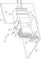
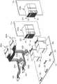
图1是根据本公开的一连接器系统的一立体图。1 is a perspective view of a connector system according to the present disclosure.
图2是处于未对接状态的图1的连接器系统的一立体图,其中一卫星连接器组件从其上分解出。2 is a perspective view of the connector system of FIG. 1 in an undocked state with a satellite connector assembly exploded therefrom.
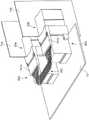
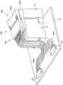
图3是图1的其中一个连接器组件的一立体图,其中壳体部件从其上分解出。FIG. 3 is a perspective view of one of the connector assemblies of FIG. 1 with the housing components exploded therefrom.
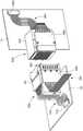
图4是图3的连接器组件的薄片体组件的一子组件的一立体图,其中一个薄片体组件从其上分解出。4 is a perspective view of a subassembly of the wafer assembly of the connector assembly of FIG. 3 with one wafer assembly exploded therefrom.
图5是图4的其中一个薄片体组件的一分解立体图。FIG. 5 is an exploded perspective view of one of the wafer assemblies of FIG. 4 .
图6是图1的另一个连接器组件的一立体图,其中卫星连接器从其上分解出。FIG. 6 is a perspective view of another connector assembly of FIG. 1 with the satellite connector exploded therefrom.
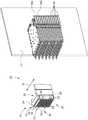
图7是图6的连接器组件的一部分的一立体图,其中壳体部件从其上分解出。FIG. 7 is a perspective view of a portion of the connector assembly of FIG. 6 with the housing components exploded therefrom.
图8是图6的连接器组件的薄片体组件的一子组件的一立体图,其中接地元件和其中一个薄片体组件从其上分解出。8 is a perspective view of a subassembly of the wafer assembly of the connector assembly of FIG. 6 with the ground element and one of the wafer assemblies exploded therefrom.
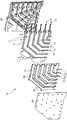
图9是图8的其中一个薄片体组件的一分解立体图。FIG. 9 is an exploded perspective view of one of the wafer assemblies of FIG. 8 .
图10是示出图3的连接器组件的薄片体以及图6的薄片体和卫星连接器组件的姿态的一示意图。FIG. 10 is a schematic diagram showing the attitude of the wafer of the connector assembly of FIG. 3 and the wafer and satellite connector assembly of FIG. 6 .
图11是根据本公开的一连接器系统的一替代实施例的一立体图。11 is a perspective view of an alternative embodiment of a connector system according to the present disclosure.
图12是处于未对接状态的图11的连接器系统的一立体图,其中一卫星连接器组件从其上分解出。12 is a perspective view of the connector system of FIG. 11 in an undocked state with a satellite connector assembly exploded therefrom.
图13是根据本公开的一连接器系统的又一替代实施例的一立体图。13 is a perspective view of yet another alternative embodiment of a connector system according to the present disclosure.
图14是处于未对接状态的图13的连接器系统的一立体图,其中一卫星连接器组件从其上分解出。14 is a perspective view of the connector system of FIG. 13 in an undocked state with a satellite connector assembly exploded therefrom.
图15是根据本公开的一连接器系统的还一替代实施例的一立体图。15 is a perspective view of yet another alternative embodiment of a connector system according to the present disclosure.
图16是处于未对接状态的图15的连接器系统的一立体图,其中一卫星连接器组件从其上分解出。16 is a perspective view of the connector system of FIG. 15 in an undocked state with a satellite connector assembly exploded therefrom.
图17是根据本公开的一连接器系统的再一替代实施例的一立体图。17 is a perspective view of yet another alternative embodiment of a connector system according to the present disclosure.
图18是处于未对接状态的图17的连接器系统的一立体图,其中一卫星连接器组件从其上分解出;18 is a perspective view of the connector system of FIG. 17 in an undocked state with a satellite connector assembly exploded therefrom;
图19是处于未对接状态的图17的连接器系统的一立体图,其中卫星连接器组件部分组装;以及19 is a perspective view of the connector system of FIG. 17 in an undocked state with the satellite connector assembly partially assembled; and
图20是与图2相似的一个立体图,但是具有组装在壳体上的一对新增的对接卫星连接器。Figure 20 is a perspective view similar to Figure 2, but with an additional pair of docking satellite connectors assembled to the housing.
具体实施方式Detailed ways
参照图1至图2,示出一正交连接器系统10。正交连接器系统10包括:一第一直角连接器组件20,安装于一第一电路元件或第一电路基板11上;以及一第二直角连接器组件60,其安装于一第二电路元件或第二电路基板13上。第一电路基板11和第二电路基板13彼此正交。1-2, an
第一连接器组件20包括一第一绝缘壳体21和多个薄片体组件30。第一壳体21具有一前对接端或前对接面22、一相反的后端或薄片体插入端或者后面或薄片体插入面23、两个侧壁24、一基板安装端或基板安装表面25以及一相反的上端或上表面26。对接面22、两个侧壁24和基板安装表面25的一部分限定一对接接口部分27,对接接口部分27配置为收容于第二连接器组件60的一插口(receptacle)或罩体105内。The
前对接面22可包括多个开口或孔28,多个开口或孔28配置为在将两个连接器组件对接在一起时收容来自第二连接器组件60的对接端子。薄片体插入端23可以是敞开的,以便多个薄片体组件30插入壳体21。除了相邻对接接口部分27之外,壳体21可以沿着基板安装表面25敞开。两个侧壁24、基板安装表面25和上表面26的长度可以不相同。例如,在一些实施例中,侧壁24可以比上表面26更短(在图2中的对接方向“A”上)。The
第一连接器组件20的多个薄片体组件30可以具有任何所需的构造。参照图3-图5,示出多个薄片体组件30的一示例性实施例。该组的多个薄片体组件30包括多个平行的薄片体组件,其中各平行薄片体组件垂直于第一电路基板11。如图5所示,各薄片体组件30包括多个高速信号端子31、多个接地元件或参考元件37、一绝缘基座元件或绝缘薄片体42以及一大体平板形的接地板或参考板44。在某些应用中,高速信号端子可以被用(re-purposed)于提供电源。The plurality of
高速信号端子31可以以相邻的对32排列,其中各对中的相邻端子之间的竖向间隔的量较小,而相邻的对之间的竖向间隔的量较大。如本文所使用的,关于第一连接器组件20的词“竖向”指的是垂直于第一电路基板11的平面的一方向,如图1至图2所示,且关于第一连接器组件20的词“水平”指的是平行于第一电路基板11的平面的一方向。The high-
各信号端子31具有:一对接端33,配置为与第二连接器组件60的一高速信号端子71对接;以及一安装尾部34,配置为电连接于第一电路基板11。在一实施例中,安装尾部34可以按机械接合第一电路基板11上的镀孔的压接引脚(press-fit pin)配置。各信号端子31的位于对接端33和安装尾部34之间的本体部35配置为改变方向,使得第一连接器组件20可以按一直角连接器配置。Each of the
如图所示,各接地元件37具有:一对接端38,配置为与第二连接器组件60的一接地端子或接地元件77对接;以及一安装尾部39,配置为电连接于第一电路基板11。接地元件37的主体40在对接端38和安装尾部39之间延伸且具有一U形横截面。各接地元件37的主体40位于相邻各对32的信号端子31的本体部35,以使端子32的对位于其相邻的接地元件37的U形横截面内,以提供屏蔽和所需的阻抗。在一些实施例中,多个接地元件37可以通过导电网板41连接。As shown, each
绝缘薄片体42支撑多个对32的竖向对齐的信号端子31,且在一实施例中,绝缘薄片体42可以围绕信号端子31的一部分嵌件成型。接地元件37然后可以诸如通过热熔接(heat staking)固定于或附接于薄片体42和大体平板状的接地板44。The insulating
可以考虑形成薄片体组件30的其他构造和其他方式。例如,在一实施例中,尽管端子31以边缘耦合的信号对32示出,但是端子31也可以按宽边耦合信号对配置,其中各对的端子31的平面部分彼此平行且相邻。在一实施例中,一端子对的各端子可以设置于其自己的薄片体内,并且将薄片体组装在一起以创建端子对。进一步地,接地元件可以设置于其自己的薄片体内,其自己的薄片体固定于信号端子的薄片体以形成薄片体组件。在一些实施例中,接地元件37和/或接地板44可以省略。Other configurations and other ways of forming the
由于第一壳体21和薄片体组件30的构造,可以容易地在第一连接器组件20上添加额外的端子31。更具体地,可以通过增加第一连接器组件20的横向宽度或侧壁24之间的距离(如图3中的箭头“B”所示)且将额外的薄片体组件30插入到第一壳体21的薄片体插入端23来添加额外的端子31。更具体地,第一壳体21可以形成有一成型模组(未示出),其允许在成型工序之前改变两个侧壁24之间的距离。结果,第一连接器组件20的端子的数量可以通过配置壳体模具以使更多的薄片体组件能够插入第一壳体21中来修改,而无对制造薄片体组件所需的模具进行修改的昂贵费用。Due to the configuration of the
参照图2至图3,第一壳体21包括一第一部分50和一第二部分51。第一部分50和第二部分51各包括在对接面22上的多个开口28。第一部分50可以与第二部分51间隔开。如图所示,第一部分50与第二部分51在平行于或沿着第一电路基板11的一方向上间隔开。第一部分50将多个薄片体组件30中的一些但不是全部收容在其内。第二部分51可以将一个以上的薄片体组件30a收容在其内。如图所示,第二部分51使一个薄片体30a收容在其内。第二部分51内的薄片体组件30a可以与第一部分50内的其他的薄片体组件30相同或不同,并且在本文中可以基于上下文与其他薄片体组件30分开引用(referenced)或共同引用。替代的功能可以由诸如电源、与其他薄片体组件30相比可支持一交替传输(alternatetransmission)阻抗的一电改性薄片体或者甚至一不同的传输介质(诸如光学介质)的组件30a来支持或提供。2 to 3 , the
在一实施例中,没有开口的一间隔部分52可以设置在第一壳体21的第一部分50和第二部分51之间。在另一实施例中,间隔部分(未示出)可以包括与对接面22的开口29相似但是没有端子的多个开口。没有端子(或至少没有对接部分)插入其内的一个或多个间隔薄片体30b可以位于该组薄片体组件30和薄片体组件30a之间并且设置于间隔部分52内。通过这样的配置,多个或一摞的薄片体组件30、30a和间隔薄片体30b可以组装在一起以创建一子组件,然后子组件通过薄片体插入端23插入第一壳体21。In one embodiment, a
尽管以将第一壳体21构造为一体成型的单件式结构进行说明,但是第一壳体21可以由组装在一起的多个部件形成。例如,参照图16,第一连接器组件320b的第一部分50和第二部分351可以是用作一单个壳体元件的两个独立壳体元件的部分。用于将两个独立的壳体元件固定在一起的结构可以占用间隔部分52的一些或全部空间。Although described as a one-piece structure in which the
参照图6至图7,第二连接器组件60包括一第二绝缘壳体61、多个薄片体组件70、一接地支撑元件85以及一卫星连接器组件90。第二壳体61具有一前对接端或前对接面62、一相反的后插入端或薄片体插入端或者后插入面或薄片体插入面63、两个侧壁64、一基板安装端或基板安装表面65以及一相反的上端或上表面66。Referring to FIGS. 6 to 7 , the
薄片体组件70的端子的对接部分延伸穿过接地支撑元件85,以便与第一连接器组件20的高速信号端子31和接地元件37对接。薄片体插入端63可以是敞开的以便多个薄片体组件70插入第二壳体61。除了相邻对接端62之外,第二壳体61可以沿基板安装表面65敞开。侧壁64和上表面66的长度可以不相同。The mating portions of the terminals of the
第二连接器组件60的薄片体组件70可以按与薄片体组件30相似或相同的方式配置。参照图7至图9,示出多个薄片体组件70的一示例性实施例。一组的薄片体组件70包括多个平行的薄片体组件70,各平行薄片体组件垂直于第二电路基板13。如图所示,各薄片体组件70包括多个高速信号端子71、多个接地元件或参考元件77、一绝缘基座元件或绝缘薄片体82以及一大体平的接地板或参考板84。The
多个高速信号端子71可以以相邻的对72排列,其中各对的相邻的端子之间的竖向间隔的量较小而在相邻的对之间的水平间隔的量较大。如本文所使用的,关于第二连接器组件60的词“竖向”指的是垂直于第二电路基板13的平面的一方向,如图1至图2所示,而关于第二连接器组件60的词“水平”指的是平行于第二电路基板13的平面的一方向。The plurality of high-
各信号端子71具有:一对接端73,配置为与第一连接器组件20的一高速信号端子31对接;以及一安装尾部74,配置为电连接于第二电路基板13。如上所述,在一实施例中,安装尾部74可以按机械接合第一电路基板11上的镀孔的压接引脚配置。各信号端子71的对接端73和安装尾部74之间的本体部75配置为改变方向,使得第二连接器组件60可以按一直角连接器配置。Each of the
如图所示,各接地元件77具有:一对接端78,配置为与第一连接器组件20的一接地端子或接地元件37对接;以及一安装尾部79,配置为电连接于第二电路基板13。接地元件77的主体80在对接端78和安装尾部79之间延伸且具有一U形横截面。各接地元件77的主体80位于相邻各对72的信号端子71的本体部75,以使端子72的对位于其相邻的接地元件77的U形横截面内,以提供屏蔽和所需的阻抗。在一些实施例中,多个接地元件77可以通过导电网板81连接。As shown, each
绝缘薄片体82支撑成对72的竖向对齐的信号端子71,且在一实施例中,绝缘薄片体82可以围绕信号端子71的一部分嵌件成型。接地元件77然后可以例如通过热熔接固定于或附接于薄片体82和大体平的接地板84。The insulating
为了允许第一连接器组件20与第二连接器组件60对接,第一连接器组件20的对接接口部分27必须配置为收容于第二连接器组件60的罩体105内。此外,第一连接器组件20和第二连接器组件60也必须具有相同的配置。更具体地,信号端子31、71和接地元件37、77的行数和列数相同,端子和接地元件之间的间隔或间距相同,且信号端子的对接端33、73和接地元件的对接端38、78也必须配置为彼此对接。To allow the
虽然形成包含端子薄片体的连接器组件在一些连接器系统中是可取的,但是将端子薄片体与正交连接器组件一起使用典型地会降低修改各连接器组件可以携带的端子的数量的灵活性。更具体地,尽管典型地可以增加第一连接器组件20的两个侧壁24之间的距离以使额外的薄片体组件30能够插入,但是修改第二连接器组件60以与这种修改的第一连接器组件对接将需要增加第二壳体61的高度(即平行于侧壁64或垂直于第二电路基板13)以及薄片体组件70的高度。While forming connector assemblies containing terminal wafers is desirable in some connector systems, the use of terminal wafers with orthogonal connector assemblies typically reduces the flexibility to modify the number of terminals that each connector assembly can carry sex. More specifically, while the distance between the two
第二连接器组件60示出不需要修改薄片体组件70的一解决方案。第二连接器组件60包括一个或多个卫星连接器组件90,其安装于第二壳体61的上表面66上且形成连接器组件60的上表面。参照图1、图2以及图6至图7,在一实施例中,卫星连接器组件90包括:一卫星连接器91,具有一卫星基座92,其中多个导电端子100安装在卫星基座92中;一柔性线缆或柔性电路元件102,具有多个导体103;以及一基板对基板电连接器120。卫星基座92具有一端子保持体93和一对接部分95。对接部分95以一大体倒U形配置,其中一连接结构或网板96在一对间隔开的侧壁97之间延伸。The
导电端子100可以具有任何结构,只要它们配置为与第一连接器组件20的薄片体组件30a的端子对接。因此,在示出的实施例中,端子100包括以与薄片体组件30a相同的图案设置的高速信号端子和接地端子或参考端子。端子100包括一对接部分或对接端(图6中未示出)和一端接部分或端接端101。各端子100的端接端101端接于线缆102的其中一个导体103。线缆102的导体103将卫星基座92内的至少一些端子100电连接于基板对基板电连接器120的至少一些端子(未示出)。The conductive terminals 100 may have any structure as long as they are configured to be mated with the terminals of the
当将卫星连接器91安装于第二壳体61上时,第二壳体61的侧壁64的一部分可以与卫星基座92的侧壁97对齐。通过缩减第二壳体61的上表面66的长度,第二壳体61的侧壁64和基板安装表面65的一部分与卫星基座92一起限定一罩体105,罩体105配置为将第一连接器组件20的对接接口部分27收容于罩体105内。When the
进一步地,缩减第二壳体61的上表面66的长度提供收容第一壳体21的间隔部分52的一开口。在一替代实施例中,上表面66可以朝向第一连接器组件20延伸与侧壁64和基板安装表面65相同(或一些其他)的长度,而第一壳体21的间隔部分52设置有沿着对接面22延伸的容纳第二壳体61的上表面66的一凹部(未示出)。Further, reducing the length of the
第二壳体61的上表面66和卫星基座92的主体93的下表面可包括对准结构或对准元件,以使卫星基座91对准第二壳体61。如图所示,第二壳体61包括多个突起或栓(peg)67,多个突起或栓(peg)67收容于卫星基座92的主体93的下表面上的同样多个的凹部或开口(未示出)内。The
连接元件或连接结构可以设置成将卫星基座92固定于第二壳体61的上表面66。可以使用任何类型的连接结构。如图所示,诸如螺丝的紧固件107可以延伸穿过卫星基座92到第二壳体61上的螺纹孔68中。可以考虑诸如压接元件或热熔接的其他连接元件或连接结构。A connecting element or connecting structure may be provided to secure the
一基板安装电连接器125可以安装在第二电路基板13上并配置为与基板对基板电连接器120对接。基板安装电连接器125的导电端子(未示出)可以电连接于第二电路基板13上的或第二电路基板13的导电迹线(未示出)。A substrate mount
如果需要,一些或全部端子100可以替换成与配置为发送和接收光信号的线缆102、基板对基板连接器120和基板安装连接器125的光连接和对应的元件。If desired, some or all of the terminals 100 may be replaced with optical connections and corresponding components to the
在组装期间,在一实施例中,在没有卫星连接器组件90的情况下,通过将一力施加于第二壳体61的上表面66和/或薄片体组件70以使高速信号端子71的安装尾部74和接地元件77的安装尾部79强迫进入第二电路基板13上的对准孔中,第二连接器组件60安装于第二电路基板13上。卫星连接器组件90安装于且固定于第二壳体61的上表面66。基板对基板连接器120然后可以对准并对接预先安装于第二电路基板13上的基板安装连接器125。在另一实施例中,可以将包括卫星连接器组件90的完全组装的第二连接器组件60安装于第二电路基板13,从而第二连接器组件60可以在安装操作之前完全组装。During assembly, in one embodiment, without the
第一连接器组件20和第二连接器组件60可包括对准结构和/或引导结构,以便在对接时两个连接器组件的对准和引导。可以使用任何所需的结构。如图所示,第一连接器组件20包括相邻对接面22的第一部分50沿各表面25、26的两个突起54和相邻间隔部分52沿各表面25、26的一单个凹部或开口55。第二连接器组件60包括沿各侧壁64的两个凹部或开口69,两个凹部或开口69配置成(例如尺寸和对准上设置成)在第一连接器组件和第二连接器组件对接在一起时与第一连接器组件20的突起54对接。如图所示,第二壳体61的上表面66在相邻第二壳体61的对接端62处不完全去除,以形成一对向内延伸的突起66a。向内延伸的突起66a配置成(例如尺寸和对准设置成)以在第一连接器组件20和第二连接器组件60对接在一起时与沿第一壳体21的各表面25、26的开口55对接。The
参照图10,其中第一连接器组件20的薄片体组件30以虚线示意性地示出,而第二连接器组件60的薄片体组件70以实线示意性地示出。可以看到的是,在连接器组件20和第二连接器组件60对接时,第一连接器组件20的薄片体组件30正交于第二连接器组件60的薄片体组件70。然而,卫星连接器组件90(以实线示出)垂直于第二连接器组件60的薄片体组件70且因此平行于第一连接器组件20的薄片体组件30。结果,在第二部分51的薄片体组件30a(以虚线示出)和卫星连接器组件90之间存在一一对应。Referring to Figure 10, the
通过这样的配置,可以容易地修改薄片体组件30a和卫星连接器组件90内的端子而不影响第一部分50的薄片体组件30和第二连接器组件60的薄片体组件70。换句话说,薄片体组件30a和卫星连接器组件90可以以任何方式配置而无需使薄片体组件30、70的改变对应。这种前预计后设计的独立的性质轻而易举地允许进行添加和修改,从而在否则可能需要重新设计和重新加工的产品配置选择中提供相当大的灵活性,产品配置选择包括诸如添加回环和交叉连接功能的独特的架构解决方案。此外,所公开的结构避免或减少了对可能在传输损耗和定时延迟方面不是最佳的间接解决方案的需求。With such a configuration, the terminals within
由于第一连接器组件20和第二连接器组件60的对接,在第一电路基板11和第二电路基板13之间将建立多个电连接。更具体地,从第一电路基板11经过第一连接器组件20的第一壳体21的第一部分50内的薄片体组件30的高速信号端子31和接地元件37,而后经过第二连接器组件60的薄片体组件70的相应的高速信号端子71和接地元件77到第二电路基板13的电连接将被建立。另外,从第一电路基板11经过第一连接器组件20的第一壳体21的第二部分51的薄片体组件30a而后经过卫星连接器组件90的端子92、经过线缆93到基板对基板电连接器120的电连接建立。通过将基板对基板电连接器120连接于基板安装连接器125,可以完成第一电路基板11和第二电路基板13之间的电连接。Due to the mating of the
可以考虑使用各种替代配置。例如,参照图11至图12,一替代实施例示出,其中,一对第一连接器组件20a、20b分别安装于第一电路基板11a、11b上,而一对第二连接器组件60a、60b安装于一单个的第二电路基板13上。一卫星连接器组件190具有一对卫星连接器191a、191b,其中一线缆202在两个卫星连接器191a、191b之间延伸。其中一个卫星连接器191a安装于一个第二连接器组件60a的第二连接器壳体61,且另一个卫星连接器191b安装于另一个连接器组件60b的第二连接器壳体61。因为线缆202在两个卫星连接器191a、191b之间延伸,所以在两个卫星连接器191a、191b之间直接建立电连接。Various alternative configurations can be considered. For example, referring to Figures 11-12, an alternative embodiment is shown in which a pair of
通过这样的配置,从第一电路基板11a经过第一连接器组件20a的第二部分51的薄片体组件30a、经过第一卫星连接器191a、经过线缆202到第二卫星连接器191b、经过第一连接器组件20b的第二部分的薄片体组件30a到第一电路基板11b的电连接建立。通过这样的配置,在第一电路基板11a和第一电路基板11b之间可以建立电连接而无需通过第二电路基板13建立电连接。With such a configuration, from the
图13至图14示出又一替代实施例,其中一卫星连接器组件290包括安装于四个第二连接器组件60a-60d的顶部上的四个卫星连接器291a-291d。卫星连接器291a-291d通过一线缆302相互连接,线缆302以任何所需的方式将四个卫星连接器的端子相互连接。更具体地,第一卫星连接器291a的端子可以连接于其他卫星连接器291b-291d的任何端子,第二卫星连接器291b的端子可以连接于其他卫星连接器291a、291c-d的任何端子,第三卫星连接器291c的端子可以连接于其他卫星连接器291a-b、291d的任何端子,而第四卫星连接器291d的端子可以连接于其他卫星连接器291a-291c的任何端子。卫星线缆组件290操作为通过安装于各自的第一电路基板11a-11d上的四个第一电连接器组件20a-20d将四个第一电路基板11a-11d连接,而信号不通过第二电路基板13。Figures 13-14 illustrate yet another alternative embodiment in which a
除了第一连接器组件20在第一壳体21的第二部分51内具有一单个薄片体组件30a且卫星连接器91具有一单行端子外,第一连接器组件20的第二部分51还可包括多个薄片体30a,且卫星连接器391可具有与薄片体30a的端子对接的多行端子。更具体地,参照图15至图16,第一连接器组件320a、320b分别安装于一第一电路基板11a、11b上。第一连接器组件320a、320b可以与上述第一连接器组件20相同,不同之处在于各第一连接器组件的第一壳体321具有一更大的第二部分351,其中第二部分351内设置有多个薄片体组件30a。如图所示,第一连接器组件320b具有用于第一部分50和第二部分351的独立的壳体部件。与上述第一连接器组件20的部件或元件相同或相似的部件或元件由相同的附图标记表示。In addition to the
卫星线缆组件390包括一对多行卫星连接器391a、391b,其中每个多行卫星连接器391a、391b配置为与第一连接器组件320a、320b的其中一个对接。多行卫星连接器391a、391b可以与上述单行卫星连接器91相同或相似,不同之处在于它们包括竖向在第二壳体61上方的多行的端子。换句话说,侧壁403比卫星基座92的侧壁97高,以容纳由卫星基座392支撑的更多行的端子。进一步地,多行尾部401从端子保持体393向后延伸。与卫星连接器组件90的部件或元件相同或相似的部件或元件由相同的附图标记表示。The satellite cable assembly 390 includes a pair of
多行卫星连接器391a、391b可以用于以上述关于图1至图9、图11至图14或这些图组合的方式将多个电路基板连接。例如,如图15至图16所示,两个多行卫星连接器391a、391b的上行尾部401a-401b通过一对线缆402a、402b连接。结果,端薄片体或上薄片体30a(如图15至图16所示)可以通过卫星连接器组件390电连接,而与上述的关于图11至图14情况一样信号无需通过第二电路基板13。此外,两个多行卫星连接器391a、391b的下行尾部402c、402d通过线缆402c-402f连接于多个基板安装连接器120。多个基板安装连接器120连接于多个基板对基板连接器(未示出),多个基板对基板连接器机械且电连接于第二电路基板13。The
在图17至图19所示的另一示例中,一第二连接器组件490可包括一多行卫星连接器491,其形成有一多部件基座492。在所示的示例中,基座492由两个或多个基座部件492a、492b形成,各基座部件492a、492b具有固定在其内的端子。端子可以端接到具有连接的基板安装连接器120的线缆502a、502b,或者端子可以端接到线缆(未示出)而该线缆端接到相邻的第二连接器组件490的其他基座部件492a、492b。In another example shown in FIGS. 17-19 , a second connector assembly 490 may include a
图20是与图2相似的一个立体图,但是具有组装在壳体上的一对新增的对接卫星连接器590、690。这对额外的对接卫星连接器590、690具有设置为对接在一起的端子与壳体。Figure 20 is a perspective view similar to Figure 2, but with an additional pair of
尽管图1至图9示出薄片体组件30a和卫星连接器组件90各具有与薄片体组件30、70相似或相同的高速信号端子和接地元件的一阵列,但是可以考虑替代结构。第一壳体21的第二部分51可包括或建立任何类型的连接,包括电源端子、光纤连接器和低速信号端子以及与图1至图5中示出的那些类似的高速信号端子和接地元件。在一些例子中,第二部分51内的连接可以不安装于与薄片体组件30、30a类似的一薄片体组件至少一薄片体组件内。卫星连接器组件90配置有将与第二部分51的那些连接对接的连接。作为一示例,返回参照图10,薄片体组件30a和卫星连接器组件90各示出为具有两个电源端子110、两个光纤连接器111以及两对高速端子112,其中接地元件113位于两对高速端子112之间并在两对高速端子112的两端上。Although FIGS. 1-9
将认识到的是,前述说明提供所公开的系统和技术的示例。然而,可以预期的是,本公开的其他实施方式可以在细节上与前述示例不同。对本公开内容或其示例的所有参照旨在参照在那时正讨论的特定示例,并不意欲暗含对本公开的范围的任何更一般的限制。所有关于某些特征的区分和贬低性的语言旨在表明对那些特征不是优先的,但不将其完全排除在本公开的范围之外,除非另有说明。It will be appreciated that the foregoing description provides examples of the disclosed systems and techniques. It is contemplated, however, that other embodiments of the present disclosure may differ in detail from the foregoing examples. All references to the present disclosure or examples thereof are intended to refer to the specific example being discussed at the time, and are not intended to imply any more general limitations on the scope of the present disclosure. All distinguishing and disparaging language regarding certain features is intended to indicate that those features are not preferred, but not to exclude them entirely from the scope of the present disclosure, unless stated otherwise.
本文中数值范围的列举仅旨在用作分别指代每个单独数值落入该范围内的简写方法,除非本文另有说明,并且每个单独数值都被并入说明书中,就好像它在本文中被单独列举一样。本文所述的所有方法可以按任何合适的顺序执行,除非本文另有说明或与上下文明显矛盾。The recitation of ranges of values herein is merely intended to serve as a shorthand method of referring individually to each individual value falling within that range, unless otherwise indicated herein, and each individual value is incorporated into the specification as if it were herein are listed separately. All methods described herein can be performed in any suitable order unless otherwise indicated herein or otherwise clearly contradicted by context.
因此,本公开包括适用法律所允许的本文随附权利要求中引用的主题的所有修改和等同物。而且,除非本文另有说明或与上下文明显矛盾,否则本公开包含所有可能变化的上述要素的任何组合。此外,本文所述的优点可能并不适用于权利要求所涵盖的所有实施例。Accordingly, this disclosure includes all modifications and equivalents of the subject matter recited in the claims appended hereto as permitted by applicable law. Furthermore, unless otherwise indicated herein or otherwise clearly contradicted by context, this disclosure encompasses any combination of the above-described elements in all possible variations. Furthermore, the advantages described herein may not apply to all embodiments covered by the claims.
Claims (11)
Applications Claiming Priority (5)
| Application Number | Priority Date | Filing Date | Title |
|---|---|---|---|
| US201962855287P | 2019-05-31 | 2019-05-31 | |
| US62/855,287 | 2019-05-31 | ||
| US16/879,788 | 2020-05-21 | ||
| US16/879,788US11114803B2 (en) | 2019-05-31 | 2020-05-21 | Connector system with wafers |
| CN202010476672.5ACN112018537B (en) | 2019-05-31 | 2020-05-29 | Connector system with wafer |
Related Parent Applications (1)
| Application Number | Title | Priority Date | Filing Date |
|---|---|---|---|
| CN202010476672.5ADivisionCN112018537B (en) | 2019-05-31 | 2020-05-29 | Connector system with wafer |
Publications (2)
| Publication Number | Publication Date |
|---|---|
| CN114583482Atrue CN114583482A (en) | 2022-06-03 |
| CN114583482B CN114583482B (en) | 2025-07-15 |
Family
ID=73506318
Family Applications (2)
| Application Number | Title | Priority Date | Filing Date |
|---|---|---|---|
| CN202010476672.5AActiveCN112018537B (en) | 2019-05-31 | 2020-05-29 | Connector system with wafer |
| CN202210276044.1AActiveCN114583482B (en) | 2019-05-31 | 2020-05-29 | Electrical connector components |
Family Applications Before (1)
| Application Number | Title | Priority Date | Filing Date |
|---|---|---|---|
| CN202010476672.5AActiveCN112018537B (en) | 2019-05-31 | 2020-05-29 | Connector system with wafer |
Country Status (2)
| Country | Link |
|---|---|
| CN (2) | CN112018537B (en) |
| TW (1) | TWI743813B (en) |
Families Citing this family (3)
| Publication number | Priority date | Publication date | Assignee | Title |
|---|---|---|---|---|
| JP7681713B2 (en)* | 2021-01-29 | 2025-05-22 | モレックス エルエルシー | BACKPLANE CONNECTOR HAVING SHIELD TERMINALS - Patent application |
| CN115864032A (en)* | 2021-09-24 | 2023-03-28 | 华为技术有限公司 | Orthogonal system architecture and network device |
| CN117096638A (en)* | 2022-05-11 | 2023-11-21 | 中兴通讯股份有限公司 | Backboard structure and communication equipment |
Citations (4)
| Publication number | Priority date | Publication date | Assignee | Title |
|---|---|---|---|---|
| CN2884588Y (en)* | 2006-02-28 | 2007-03-28 | 上海瓯宝电子科技有限公司 | Combined connector |
| US20070155241A1 (en)* | 2005-12-31 | 2007-07-05 | Erni Elektroapparate Gmbh | Plug-and-socket connector |
| CN104718666A (en)* | 2012-08-27 | 2015-06-17 | 富加宜(亚洲)私人有限公司 | High speed electrical connector |
| CN108352633A (en)* | 2015-12-14 | 2018-07-31 | 莫列斯有限公司 | It omits the back panel connector of earth shield body and uses its system |
Family Cites Families (9)
| Publication number | Priority date | Publication date | Assignee | Title |
|---|---|---|---|---|
| DE19535822A1 (en)* | 1995-09-26 | 1997-03-27 | Amp Holland | Arrangement for connecting an electrical connector to a complementary connector |
| JP4958183B2 (en)* | 2006-01-20 | 2012-06-20 | タイコ エレクトロニクス ネーデルランド ビーヴイ | Electrical connector |
| MY155071A (en)* | 2008-12-12 | 2015-08-28 | Molex Inc | Resonance modifying connector |
| WO2011050277A2 (en)* | 2009-10-23 | 2011-04-28 | Molex Incorporated | Right angle adaptor |
| US8814595B2 (en)* | 2011-02-18 | 2014-08-26 | Amphenol Corporation | High speed, high density electrical connector |
| US8894442B2 (en)* | 2012-04-26 | 2014-11-25 | Tyco Electronics Corporation | Contact modules for receptacle assemblies |
| US9548570B2 (en)* | 2013-07-23 | 2017-01-17 | Molex, Llc | Direct backplane connector |
| CN105449461B (en)* | 2014-09-30 | 2017-09-22 | 莫列斯公司 | Electric connector |
| US10128619B2 (en)* | 2017-01-27 | 2018-11-13 | Te Connectivity Corporation | Ground shield for a contact module |
- 2020
- 2020-05-28TWTW109117800Apatent/TWI743813B/enactive
- 2020-05-29CNCN202010476672.5Apatent/CN112018537B/enactiveActive
- 2020-05-29CNCN202210276044.1Apatent/CN114583482B/enactiveActive
Patent Citations (4)
| Publication number | Priority date | Publication date | Assignee | Title |
|---|---|---|---|---|
| US20070155241A1 (en)* | 2005-12-31 | 2007-07-05 | Erni Elektroapparate Gmbh | Plug-and-socket connector |
| CN2884588Y (en)* | 2006-02-28 | 2007-03-28 | 上海瓯宝电子科技有限公司 | Combined connector |
| CN104718666A (en)* | 2012-08-27 | 2015-06-17 | 富加宜(亚洲)私人有限公司 | High speed electrical connector |
| CN108352633A (en)* | 2015-12-14 | 2018-07-31 | 莫列斯有限公司 | It omits the back panel connector of earth shield body and uses its system |
Also Published As
| Publication number | Publication date |
|---|---|
| CN112018537A (en) | 2020-12-01 |
| TWI743813B (en) | 2021-10-21 |
| TW202101830A (en) | 2021-01-01 |
| CN114583482B (en) | 2025-07-15 |
| CN112018537B (en) | 2022-02-01 |
Similar Documents
| Publication | Publication Date | Title |
|---|---|---|
| TWI760222B (en) | Backplane connector | |
| CN114556705B (en) | Connector components | |
| US20230047149A1 (en) | Connector assembly | |
| CN101432934B (en) | electrical connector | |
| TWI858382B (en) | Electrical connector and assembly thereof | |
| JP3889447B2 (en) | Connector assembly having shielded module and method of manufacturing the same | |
| CN100391058C (en) | high speed differential signal connector with interstitial ground appearance | |
| CN102176564B (en) | There is the electric connector system of electrical connection and guidance feature | |
| US7785152B2 (en) | High density connector having two-leveled contact interface | |
| US8366458B2 (en) | Electrical power connector system | |
| US8353728B2 (en) | Receptacle connector having contact modules and plug connector having a paddle board | |
| TWM453990U (en) | Mezzanine connector with terminal brick | |
| CN110299630A (en) | Electric coupler component | |
| US11114803B2 (en) | Connector system with wafers | |
| CN111525307B (en) | Dual connector assembly for circuit board | |
| TW202209765A (en) | Contact module for a header assembly | |
| CN114583482B (en) | Electrical connector components | |
| CN102106042A (en) | Electrical connectors and assemblies having socket members | |
| CN117317637A (en) | Electrical connector assembly and method of manufacturing the same | |
| CN117317712B (en) | Electric connector | |
| CN117317644B (en) | Electric connector | |
| TWM664848U (en) | Terminal module and backplane connector | |
| CN115706371A (en) | Direct insertion type orthogonal board-to-board connector system | |
| CN117317659A (en) | Socket assembly | |
| CN117317638A (en) | Electric connector assembly |
Legal Events
| Date | Code | Title | Description |
|---|---|---|---|
| PB01 | Publication | ||
| PB01 | Publication | ||
| SE01 | Entry into force of request for substantive examination | ||
| SE01 | Entry into force of request for substantive examination | ||
| GR01 | Patent grant | ||
| GR01 | Patent grant |