CN114582958B - Manufacturing method of semiconductor structure and semiconductor structure - Google Patents
Manufacturing method of semiconductor structure and semiconductor structureDownload PDFInfo
- Publication number
- CN114582958B CN114582958BCN202210462531.7ACN202210462531ACN114582958BCN 114582958 BCN114582958 BCN 114582958BCN 202210462531 ACN202210462531 ACN 202210462531ACN 114582958 BCN114582958 BCN 114582958B
- Authority
- CN
- China
- Prior art keywords
- layer
- dielectric layer
- electrode
- support structure
- forming
- Prior art date
- Legal status (The legal status is an assumption and is not a legal conclusion. Google has not performed a legal analysis and makes no representation as to the accuracy of the status listed.)
- Active
Links
Images


Classifications
- H—ELECTRICITY
- H10—SEMICONDUCTOR DEVICES; ELECTRIC SOLID-STATE DEVICES NOT OTHERWISE PROVIDED FOR
- H10D—INORGANIC ELECTRIC SEMICONDUCTOR DEVICES
- H10D62/00—Semiconductor bodies, or regions thereof, of devices having potential barriers
- H10D62/10—Shapes, relative sizes or dispositions of the regions of the semiconductor bodies; Shapes of the semiconductor bodies
- H10D62/113—Isolations within a component, i.e. internal isolations
- H10D62/115—Dielectric isolations, e.g. air gaps
- H10D62/116—Dielectric isolations, e.g. air gaps adjoining the input or output regions of field-effect devices, e.g. adjoining source or drain regions
- H—ELECTRICITY
- H10—SEMICONDUCTOR DEVICES; ELECTRIC SOLID-STATE DEVICES NOT OTHERWISE PROVIDED FOR
- H10B—ELECTRONIC MEMORY DEVICES
- H10B12/00—Dynamic random access memory [DRAM] devices
- H—ELECTRICITY
- H10—SEMICONDUCTOR DEVICES; ELECTRIC SOLID-STATE DEVICES NOT OTHERWISE PROVIDED FOR
- H10D—INORGANIC ELECTRIC SEMICONDUCTOR DEVICES
- H10D30/00—Field-effect transistors [FET]
- H10D30/01—Manufacture or treatment
- H10D30/021—Manufacture or treatment of FETs having insulated gates [IGFET]
- H10D30/027—Manufacture or treatment of FETs having insulated gates [IGFET] of lateral single-gate IGFETs
- H—ELECTRICITY
- H10—SEMICONDUCTOR DEVICES; ELECTRIC SOLID-STATE DEVICES NOT OTHERWISE PROVIDED FOR
- H10D—INORGANIC ELECTRIC SEMICONDUCTOR DEVICES
- H10D30/00—Field-effect transistors [FET]
- H10D30/60—Insulated-gate field-effect transistors [IGFET]
- H10D30/637—Lateral IGFETs having no inversion channels, e.g. buried channel lateral IGFETs, normally-on lateral IGFETs or depletion-mode lateral IGFETs
- H—ELECTRICITY
- H10—SEMICONDUCTOR DEVICES; ELECTRIC SOLID-STATE DEVICES NOT OTHERWISE PROVIDED FOR
- H10D—INORGANIC ELECTRIC SEMICONDUCTOR DEVICES
- H10D62/00—Semiconductor bodies, or regions thereof, of devices having potential barriers
- H10D62/10—Shapes, relative sizes or dispositions of the regions of the semiconductor bodies; Shapes of the semiconductor bodies
- H10D62/13—Semiconductor regions connected to electrodes carrying current to be rectified, amplified or switched, e.g. source or drain regions
- H10D62/149—Source or drain regions of field-effect devices
- H10D62/151—Source or drain regions of field-effect devices of IGFETs
- H—ELECTRICITY
- H10—SEMICONDUCTOR DEVICES; ELECTRIC SOLID-STATE DEVICES NOT OTHERWISE PROVIDED FOR
- H10D—INORGANIC ELECTRIC SEMICONDUCTOR DEVICES
- H10D64/00—Electrodes of devices having potential barriers
- H10D64/20—Electrodes characterised by their shapes, relative sizes or dispositions
- H10D64/27—Electrodes not carrying the current to be rectified, amplified, oscillated or switched, e.g. gates
- H10D64/311—Gate electrodes for field-effect devices
- H10D64/411—Gate electrodes for field-effect devices for FETs
- H10D64/511—Gate electrodes for field-effect devices for FETs for IGFETs
- H10D64/512—Disposition of the gate electrodes, e.g. buried gates
Landscapes
- Internal Circuitry In Semiconductor Integrated Circuit Devices (AREA)
- Semiconductor Memories (AREA)
Abstract
Description
Translated fromChinese技术领域technical field
本公开涉及半导体技术领域,尤其涉及一种半导体结构的制作方法及半导体结构。The present disclosure relates to the field of semiconductor technology, and in particular, to a method for fabricating a semiconductor structure and a semiconductor structure.
背景技术Background technique
动态随机存取存储器(DRAM,Dynamic Random Access Memory)具有体积小、集成度高、功耗低的优点,同时存取速度比只读存储器(ROM,Read Only Memory)快。随着半导体行业的不断发展,对半导体结构的要求越来越高。Dynamic random access memory (DRAM, Dynamic Random Access Memory) has the advantages of small size, high integration, low power consumption, and access speed is faster than read only memory (ROM, Read Only Memory). With the continuous development of the semiconductor industry, the requirements for semiconductor structures are getting higher and higher.
其中,DRAM芯片主要由晶体管和电容组成,为提高DRAM芯片的存储密度,电容器的尺寸越来越小。而随着电容器尺寸的缩小,电容结构在形成过程中先形成下电极,形成的下电极与支撑层之间的深宽比越来越大,导致后续形成介电层的材料的填充能力下降,严重时会造成电容底部无法填入介质层或者填入的介质层的厚度达不到要求,从而造成严重的漏电问题。Among them, DRAM chips are mainly composed of transistors and capacitors. In order to improve the storage density of DRAM chips, the size of capacitors is getting smaller and smaller. As the size of the capacitor shrinks, the lower electrode is first formed during the formation of the capacitor structure, and the aspect ratio between the formed lower electrode and the supporting layer becomes larger and larger, resulting in a decrease in the filling ability of the material for the subsequent formation of the dielectric layer. In severe cases, the bottom of the capacitor cannot be filled with the dielectric layer or the thickness of the filled dielectric layer cannot meet the requirements, resulting in serious leakage problems.
发明内容SUMMARY OF THE INVENTION
以下是对本公开详细描述的主题的概述。本概述并非是为了限制权利要求的保护范围。The following is an overview of the subject matter detailed in this disclosure. This summary is not intended to limit the scope of protection of the claims.
本公开提供了一种半导体结构的制作方法及半导体结构。The present disclosure provides a method for fabricating a semiconductor structure and a semiconductor structure.
本公开的第一方面提供了一种半导体结构的制作方法,所述半导体结构的制作方法包括:A first aspect of the present disclosure provides a method for fabricating a semiconductor structure, and the method for fabricating the semiconductor structure includes:
提供基底,所述基底内设有多个分立设置的接触结构;providing a substrate with a plurality of discrete contact structures disposed in the substrate;
于所述基底上形成第一支撑结构和牺牲层;forming a first support structure and a sacrificial layer on the substrate;
形成第一通孔,所述第一通孔的底部暴露所述接触结构的顶面;forming a first through hole, and the bottom of the first through hole exposes the top surface of the contact structure;
于所述第一通孔的侧壁形成介电层,所述第一通孔内的所述介电层之间形成第二通孔;forming a dielectric layer on the sidewall of the first through hole, and forming a second through hole between the dielectric layers in the first through hole;
于所述第二通孔内形成第一电极结构,所述第一电极结构覆盖部分所述接触结构表面和位于所述第二通孔内的所述介电层的侧壁,每个所述第一电极结构对应不同的接触结构;A first electrode structure is formed in the second through hole, the first electrode structure covers part of the surface of the contact structure and the sidewall of the dielectric layer in the second through hole, each of the The first electrode structures correspond to different contact structures;
在所述第一电极结构上形成第二支撑结构;forming a second support structure on the first electrode structure;
去除所述牺牲层、部分所述第一支撑结构、部分所述第二支撑结构;removing the sacrificial layer, part of the first support structure, and part of the second support structure;
形成第二电极结构,所述第二电极结构至少覆盖部分所述介电层表面。A second electrode structure is formed, and the second electrode structure covers at least part of the surface of the dielectric layer.
根据本公开的一些实施例,于所述第二通孔内形成第一电极结构,包括:According to some embodiments of the present disclosure, forming a first electrode structure in the second through hole includes:
于所述第二通孔的侧壁和底部形成第一电极层,所述第二通孔内的所述第一电极层形成第三通孔;forming a first electrode layer on the sidewall and bottom of the second through hole, and forming a third through hole in the first electrode layer in the second through hole;
于所述第三通孔内形成缓冲层,其中,所述缓冲层和所述第一电极层形成所述第一电极结构。A buffer layer is formed in the third through hole, wherein the buffer layer and the first electrode layer form the first electrode structure.
根据本公开的一些实施例,于所述第二通孔的侧壁和底部形成第一电极层,包括:According to some embodiments of the present disclosure, forming a first electrode layer on the sidewall and bottom of the second through hole includes:
于所述第二通孔内形成第一初始电极层,所述第一初始电极层延伸至所述第二通孔外,并覆盖所述介电层的顶面;forming a first initial electrode layer in the second through hole, the first initial electrode layer extending to the outside of the second through hole and covering the top surface of the dielectric layer;
将位于所述介电层的顶面的部分所述第一初始电极层断开,被保留下来的所述第一初始电极层形成所述第一电极层。A part of the first initial electrode layer located on the top surface of the dielectric layer is disconnected, and the remaining first initial electrode layer forms the first electrode layer.
根据本公开的一些实施例,将位于所述介电层的顶面的部分所述第一初始电极层断开,包括:According to some embodiments of the present disclosure, disconnecting a portion of the first initial electrode layer on the top surface of the dielectric layer includes:
于所述第一初始电极层上形成依次层叠设置的第一介质层、隔离层和掩膜层;forming a first dielectric layer, an isolation layer and a mask layer which are stacked in sequence on the first initial electrode layer;
图形化所述掩膜层,以在所述掩膜层上形成掩膜开口;patterning the mask layer to form mask openings on the mask layer;
通过所述掩膜开口刻蚀部分所述隔离层、部分所述第一介质层和部分所述第一初始电极层;Etching part of the isolation layer, part of the first dielectric layer and part of the first initial electrode layer through the mask opening;
将位于所述介电层的顶面的部分所述第一初始电极层断开。A portion of the first initial electrode layer located on the top surface of the dielectric layer is disconnected.
根据本公开的一些实施例,所述介电层覆盖所述第一支撑结构的部分顶面。According to some embodiments of the present disclosure, the dielectric layer covers a portion of the top surface of the first support structure.
根据本公开的一些实施例,于所述第一通孔的侧壁形成介电层,包括:According to some embodiments of the present disclosure, forming a dielectric layer on the sidewall of the first via includes:
于所述第一通孔内形成初始介电层,所述初始介电层延伸至所述第一通孔外,并覆盖所述第一支撑结构的顶面;forming an initial dielectric layer in the first through hole, the initial dielectric layer extending outside the first through hole and covering the top surface of the first support structure;
去除位于所述第一通孔底部的所述初始介电层,被保留下来的所述初始介电层形成中间介电层,所述第一通孔内的所述中间介电层之间形成所述第二通孔;removing the initial dielectric layer located at the bottom of the first through hole, and the remaining initial dielectric layer forms an intermediate dielectric layer, which is formed between the intermediate dielectric layers in the first through hole the second through hole;
去除相邻的所述第一通孔之间的所述第一支撑结构的顶面的部分所述中间介电层,形成所述介电层。Part of the intermediate dielectric layer on the top surface of the first support structure between the adjacent first through holes is removed to form the dielectric layer.
根据本公开的一些实施例,去除所述牺牲层、部分所述第一支撑结构、部分所述第二支撑结构,包括:According to some embodiments of the present disclosure, removing the sacrificial layer, part of the first support structure, and part of the second support structure includes:
于所述第二支撑结构上形成多个分立设置的第四通孔,所述第四通孔贯穿所述第二支撑结构、所述介电层、所述第一支撑结构和所述牺牲层;A plurality of discrete fourth through holes are formed on the second support structure, the fourth through holes penetrate through the second support structure, the dielectric layer, the first support structure and the sacrificial layer ;
去除所述牺牲层,暴露出所述介电层的部分侧壁,其中,被保留下来的所述第一支撑结构和所述第二支撑结构形成支撑结构。Removing the sacrificial layer exposes a portion of the sidewall of the dielectric layer, wherein the remaining first support structure and the second support structure form a support structure.
根据本公开的一些实施例,形成第二电极结构,包括:According to some embodiments of the present disclosure, forming a second electrode structure includes:
形成所述第二电极结构,所述第二电极结构包裹所述支撑结构的部分侧壁和所述介电层的部分侧壁。The second electrode structure is formed, and the second electrode structure wraps a portion of the sidewall of the support structure and a portion of the sidewall of the dielectric layer.
根据本公开的一些实施例,于所述基底上形成第一支撑结构和牺牲层,包括:According to some embodiments of the present disclosure, forming a first support structure and a sacrificial layer on the substrate includes:
于所述基底上形成层叠设置的第一初始支撑层、第一牺牲层、第二初始支撑层、第二牺牲层和第三初始支撑层。A first initial support layer, a first sacrificial layer, a second initial support layer, a second sacrificial layer and a third initial support layer are formed on the substrate.
根据本公开的一些实施例,形成第一通孔,包括:According to some embodiments of the present disclosure, forming the first through hole includes:
于所述第一支撑结构上形成依次层叠设置的第二介质层和第三牺牲层;forming a second dielectric layer and a third sacrificial layer stacked in sequence on the first support structure;
图形化所述第三牺牲层,以在所述第三牺牲层上形成多个间隔设置的第五通孔;patterning the third sacrificial layer to form a plurality of spaced fifth through holes on the third sacrificial layer;
沿所述第五通孔刻蚀所述第二介质层,以在所述第二介质层内形成多个间隔设置的第六通孔;etching the second dielectric layer along the fifth through holes to form a plurality of sixth through holes spaced apart in the second dielectric layer;
去除剩余的所述第三牺牲层;removing the remaining third sacrificial layer;
沿所述第六通孔刻蚀所述第一支撑结构,以在所述第一支撑结构上形成所述第一通孔,多个所述第一通孔间隔设置;etching the first support structure along the sixth through hole to form the first through hole on the first support structure, and a plurality of the first through holes are arranged at intervals;
去除剩余的所述第二介质层。The remaining second dielectric layer is removed.
根据本公开的一些实施例,图形化所述第三牺牲层,以在所述第三牺牲层上形成多个间隔设置的第五通孔,包括:According to some embodiments of the present disclosure, patterning the third sacrificial layer to form a plurality of spaced fifth through holes on the third sacrificial layer, including:
于所述第三牺牲层上形成层叠设置的第三介质层和第一隔离层;forming a stacked third dielectric layer and a first isolation layer on the third sacrificial layer;
图形化所述第三介质层和所述第一隔离层,以在所述第一隔离层和所述第三介质层内形成第七通孔;patterning the third dielectric layer and the first isolation layer to form seventh through holes in the first isolation layer and the third dielectric layer;
沿所述第七通孔刻蚀所述第三牺牲层,以在所述第三牺牲层上形成所述第五通孔;etching the third sacrificial layer along the seventh through hole to form the fifth through hole on the third sacrificial layer;
去除剩余的所述第三介质层和所述第一隔离层。The remaining third dielectric layer and the first isolation layer are removed.
本公开的第二方面提供了一种半导体结构,包括:A second aspect of the present disclosure provides a semiconductor structure comprising:
基底,所述基底设有多个分立设置的接触结构;a substrate, the substrate is provided with a plurality of discretely arranged contact structures;
第一电极结构,所述第一电极结构与所述接触结构连接;a first electrode structure, the first electrode structure is connected to the contact structure;
介电层,所述介电层设在所述第一电极结构的外侧壁;a dielectric layer, the dielectric layer is provided on the outer sidewall of the first electrode structure;
第一支撑结构,所述第一支撑结构位于所述介电层两侧的侧壁上,其中,所述介电层还覆盖所述第一支撑结构的部分顶面;a first support structure, the first support structure is located on the sidewalls on both sides of the dielectric layer, wherein the dielectric layer also covers part of the top surface of the first support structure;
第二支撑结构,所述第二支撑结构设在所述介电层的顶面;a second support structure, the second support structure is provided on the top surface of the dielectric layer;
第二电极结构,所述第二电极结构覆盖所述第一支撑结构、所述第二支撑结构和所述介电层外表面。A second electrode structure covering the first support structure, the second support structure and the outer surface of the dielectric layer.
根据本公开的一些实施例,所述介电层包括第一介电层和第二介电层;According to some embodiments of the present disclosure, the dielectric layer includes a first dielectric layer and a second dielectric layer;
所述第一介电层设在所述第一电极结构的外侧壁上;the first dielectric layer is provided on the outer sidewall of the first electrode structure;
所述第二介电层与所述第一介电层连接,所述第二介电层覆盖整个所述第一支撑结构的顶面,且所述第二介电层位于所述第一支撑结构和所述第二支撑结构之间。The second dielectric layer is connected to the first dielectric layer, the second dielectric layer covers the entire top surface of the first support structure, and the second dielectric layer is located on the first support between the structure and the second support structure.
根据本公开的一些实施例,所述介电层包括第三介电层;According to some embodiments of the present disclosure, the dielectric layer includes a third dielectric layer;
所述第三介电层设在所述第一电极结构的外侧壁上,且所述第三介电层的顶面与所述第一电极结构的顶面平齐。The third dielectric layer is disposed on the outer sidewall of the first electrode structure, and the top surface of the third dielectric layer is flush with the top surface of the first electrode structure.
根据本公开的一些实施例,所述介电层包括第四介电层和第五介电层;According to some embodiments of the present disclosure, the dielectric layer includes a fourth dielectric layer and a fifth dielectric layer;
所述第四介电层设在所述第一电极结构的外侧壁上;the fourth dielectric layer is provided on the outer sidewall of the first electrode structure;
所述第五介电层与所述第四介电层连接,所述第五介电层覆盖部分所述第一支撑结构的顶面,且所述第五介电层位于所述第一支撑结构和所述第二支撑结构之间。The fifth dielectric layer is connected to the fourth dielectric layer, the fifth dielectric layer covers part of the top surface of the first support structure, and the fifth dielectric layer is located on the first support between the structure and the second support structure.
根据本公开的一些实施例,所述第一电极结构包括第一电极层和缓冲层;According to some embodiments of the present disclosure, the first electrode structure includes a first electrode layer and a buffer layer;
所述第一电极层与所述接触结构连接,并包裹所述缓冲层,其中,所述第一电极层的外侧壁与所述介电层连接。The first electrode layer is connected to the contact structure and wraps the buffer layer, wherein the outer sidewall of the first electrode layer is connected to the dielectric layer.
根据本公开的一些实施例,所述缓冲层的材质包括多晶硅、掺杂碳的氮化硅或掺杂碳的氧化硅中的一种或多种。According to some embodiments of the present disclosure, the material of the buffer layer includes one or more of polysilicon, carbon-doped silicon nitride, or carbon-doped silicon oxide.
本公开实施例所提供的半导体结构的制作方法及半导体结构中,先在第一通孔的侧壁和第一支撑结构的部分顶面上形成介电层,有效提高了由高K材料制成的介电层的填充能力和填充质量,从而有效提高了后续所形成的第一电极结构和第二电极结构之间的绝缘性,防止第一电极结构和第二电极结构之间发生漏电,从而提高了半导体结构的性能和良率。In the method for fabricating a semiconductor structure and the semiconductor structure provided by the embodiments of the present disclosure, a dielectric layer is first formed on the sidewall of the first through hole and part of the top surface of the first support structure, which effectively improves the efficiency of the semiconductor structure made of high-K materials. The filling capacity and filling quality of the dielectric layer can effectively improve the insulation between the first electrode structure and the second electrode structure formed subsequently, and prevent the leakage between the first electrode structure and the second electrode structure. The performance and yield of semiconductor structures are improved.
在阅读并理解了附图和详细描述后,可以明白其他方面。Other aspects will become apparent upon reading and understanding of the drawings and detailed description.
附图说明Description of drawings
并入到说明书中并且构成说明书的一部分的附图示出了本公开的实施例,并且与描述一起用于解释本公开实施例的原理。在这些附图中,类似的附图标记用于表示类似的要素。下面描述中的附图是本公开的一些实施例,而不是全部实施例。对于本领域技术人员来讲,在不付出创造性劳动的前提下,可以根据这些附图获得其他的附图。The accompanying drawings, which are incorporated in and constitute a part of the specification, illustrate the embodiments of the present disclosure and together with the description serve to explain the principles of the embodiments of the present disclosure. In the figures, like reference numerals are used to refer to like elements. The drawings in the following description are of some, but not all, embodiments of the present disclosure. For those skilled in the art, other drawings can be obtained from these drawings without creative effort.
图1是根据一示例性实施例示出的半导体结构的制作方法的流程图。FIG. 1 is a flow chart of a method for fabricating a semiconductor structure according to an exemplary embodiment.
图2是根据一示例性实施例示出的半导体结构的制作方法中形成第一光刻胶层的示意图。FIG. 2 is a schematic diagram of forming a first photoresist layer in a method for fabricating a semiconductor structure according to an exemplary embodiment.
图3是根据一示例性实施例示出的半导体结构的制作方法中形成第八通孔的示意图。FIG. 3 is a schematic diagram of forming an eighth through hole in a method for fabricating a semiconductor structure according to an exemplary embodiment.
图4是根据一示例性实施例示出的半导体结构的制作方法中形成第一掩膜层的示意图。FIG. 4 is a schematic diagram of forming a first mask layer in a method for fabricating a semiconductor structure according to an exemplary embodiment.
图5是根据一示例性实施例示出的半导体结构的制作方法中形成第一掩膜柱的示意图。FIG. 5 is a schematic diagram of forming a first mask pillar in a method for fabricating a semiconductor structure according to an exemplary embodiment.
图6是根据一示例性实施例示出的半导体结构的制作方法中形成第三氮氧化硅层的示意图。FIG. 6 is a schematic diagram of forming a third silicon oxynitride layer in a method for fabricating a semiconductor structure according to an exemplary embodiment.
图7是根据一示例性实施例示出的半导体结构的制作方法中形成第二掩膜层的示意图。FIG. 7 is a schematic diagram of forming a second mask layer in a method for fabricating a semiconductor structure according to an exemplary embodiment.
图8是根据一示例性实施例示出的半导体结构的制作方法中去除顶面的第二掩膜层的示意图。FIG. 8 is a schematic diagram of removing the second mask layer on the top surface in a method for fabricating a semiconductor structure according to an exemplary embodiment.
图9是根据一示例性实施例示出的半导体结构的制作方法中形成第二掩膜柱的示意图。FIG. 9 is a schematic diagram of forming a second mask pillar in a method for fabricating a semiconductor structure according to an exemplary embodiment.
图10是根据一示例性实施例示出的半导体结构的制作方法中形成第七通孔的示意图。FIG. 10 is a schematic diagram of forming a seventh through hole in a method for fabricating a semiconductor structure according to an exemplary embodiment.
图11是根据一示例性实施例示出的半导体结构的制作方法中形成第五通孔的示意图。FIG. 11 is a schematic diagram of forming a fifth through hole in a method for fabricating a semiconductor structure according to an exemplary embodiment.
图12是根据一示例性实施例示出的半导体结构的制作方法中形成第六通孔的示意图。FIG. 12 is a schematic diagram of forming a sixth through hole in a method for fabricating a semiconductor structure according to an exemplary embodiment.
图13是根据一示例性实施例示出的半导体结构的制作方法中形成第一通孔的示意图。FIG. 13 is a schematic diagram of forming a first through hole in a method for fabricating a semiconductor structure according to an exemplary embodiment.
图14是根据一示例性实施例示出的半导体结构的制作方法中形成初始介电层的示意图。FIG. 14 is a schematic diagram of forming an initial dielectric layer in a method for fabricating a semiconductor structure according to an exemplary embodiment.
图15是根据一示例性实施例示出的半导体结构的制作方法中形成第二通孔的示意图。FIG. 15 is a schematic diagram of forming a second through hole in a method for fabricating a semiconductor structure according to an exemplary embodiment.
图16是根据一示例性实施例示出的半导体结构的制作方法中形成第一初始电极层的示意图。FIG. 16 is a schematic diagram of forming a first initial electrode layer in a method for fabricating a semiconductor structure according to an exemplary embodiment.
图17是根据一示例性实施例示出的半导体结构的制作方法中形成掩膜层的示意图。FIG. 17 is a schematic diagram of forming a mask layer in a method for fabricating a semiconductor structure according to an exemplary embodiment.
图18是根据一示例性实施例示出的半导体结构的制作方法中形成第一电极层的示意图。FIG. 18 is a schematic diagram of forming a first electrode layer in a method for fabricating a semiconductor structure according to an exemplary embodiment.
图19是根据一示例性实施例示出的半导体结构的制作方法中形成初始缓冲层的示意图。FIG. 19 is a schematic diagram of forming an initial buffer layer in a method for fabricating a semiconductor structure according to an exemplary embodiment.
图20是根据一示例性实施例示出的半导体结构的制作方法中形成缓冲层的示意图。FIG. 20 is a schematic diagram of forming a buffer layer in a method for fabricating a semiconductor structure according to an exemplary embodiment.
图21是根据一示例性实施例示出的半导体结构的制作方法中形成第四掩膜层的示意图。FIG. 21 is a schematic diagram of forming a fourth mask layer in a method for fabricating a semiconductor structure according to an exemplary embodiment.
图22是根据一示例性实施例示出的半导体结构的制作方法中形成第四通孔的示意图。FIG. 22 is a schematic diagram of forming a fourth through hole in a method for fabricating a semiconductor structure according to an exemplary embodiment.
图23是根据一示例性实施例示出的半导体结构的制作方法中形成支撑结构的示意图。FIG. 23 is a schematic diagram of forming a support structure in a method for fabricating a semiconductor structure according to an exemplary embodiment.
图24是根据一示例性实施例示出的半导体结构的制作方法中形成第二电极结构的示意图。FIG. 24 is a schematic diagram of forming a second electrode structure in a method for fabricating a semiconductor structure according to an exemplary embodiment.
图25是根据一示例性实施例示出的半导体结构的制作方法中介电层的示意图。FIG. 25 is a schematic diagram of a dielectric layer in a method for fabricating a semiconductor structure according to an exemplary embodiment.
图26是根据一示例性实施例示出的半导体结构的制作方法中介电层的示意图。FIG. 26 is a schematic diagram of a dielectric layer in a method for fabricating a semiconductor structure according to an exemplary embodiment.
附图标记:Reference number:
10、基底;20、接触结构;30、第一支撑结构;31、第一初始支撑层;32、第二初始支撑层;33、第三初始支撑层;40、牺牲层;41、第一牺牲层;42、第二牺牲层;50、第一通孔;60、第二介质层;70、第三牺牲层;80、第五通孔;90、第六通孔;100、第三介质层;110、第一隔离层;120、第七通孔;130、第一旋涂碳层;140、第一氮氧化硅层;141、第一光刻胶层;150、第八通孔;160、第一掩膜层;170、第一掩膜柱;180、第二旋涂碳层;190、第二氮氧化硅层;200、第三旋涂碳层;210、第三氮氧化硅层;220、第九通孔;230、第二掩膜层;240、第二掩膜柱;250、介电层;251、初始介电层;252、中间介电层;253、第一介电层;254、第二介电层;255、第三介电层;256、第四介电层;257、第五介电层;260、第二通孔;270、第一电极结构;271、第一电极层;272、缓冲层;280、第三通孔;290、第一介质层;300、隔离层;310、掩膜层;320、第二支撑结构;321、第四旋涂碳层;322、第四氮氧化硅层;323、第四掩膜层;330、第四通孔;340、支撑结构;350、第二电极结构;2711、第一初始电极层;2721、初始缓冲层。10, substrate; 20, contact structure; 30, first support structure; 31, first initial support layer; 32, second initial support layer; 33, third initial support layer; 40, sacrificial layer; 41, first sacrificial layer layer; 42, the second sacrificial layer; 50, the first through hole; 60, the second dielectric layer; 70, the third sacrificial layer; 80, the fifth through hole; 90, the sixth through hole; 100, the third dielectric layer 110, the first isolation layer; 120, the seventh through hole; 130, the first spin-on carbon layer; 140, the first silicon oxynitride layer; 141, the first photoresist layer; 150, the eighth through hole; 160 170, the first mask post; 180, the second spin-on carbon layer; 190, the second silicon oxynitride layer; 200, the third spin-on carbon layer; 210, the third silicon oxynitride layer 220, the ninth through hole; 230, the second mask layer; 240, the second mask column; 250, the dielectric layer; 251, the initial dielectric layer; 252, the intermediate dielectric layer; 253, the first dielectric layer; 254, the second dielectric layer; 255, the third dielectric layer; 256, the fourth dielectric layer; 257, the fifth dielectric layer; 260, the second through hole; 270, the first electrode structure; 271, 272, buffer layer; 280, third through hole; 290, first dielectric layer; 300, isolation layer; 310, mask layer; 320, second support structure; 321, fourth spin-on carbon layer 322, the fourth silicon oxynitride layer; 323, the fourth mask layer; 330, the fourth through hole; 340, the support structure; 350, the second electrode structure; 2711, the first initial electrode layer; 2721, the initial buffer layer .
具体实施方式Detailed ways
为使本公开实施例的目的、技术方案和优点更加清楚,下面将结合本公开实施例中的附图,对公开实施例中的技术方案进行清楚、完整地描述,显然,所描述的实施例是本公开一部分实施例,而不是全部的实施例。基于本公开中的实施例,本领域技术人员在没有做出创造性劳动前提下所获得的所有其他实施例,都属于本公开保护的范围。需要说明的是,在不冲突的情况下,本公开中的实施例及实施例中的特征可以相互任意组合。In order to make the purposes, technical solutions and advantages of the embodiments of the present disclosure more clear, the technical solutions in the disclosed embodiments will be clearly and completely described below with reference to the accompanying drawings in the embodiments of the present disclosure. Obviously, the described embodiments These are some, but not all, embodiments of the present disclosure. Based on the embodiments in the present disclosure, all other embodiments obtained by those skilled in the art without creative efforts shall fall within the protection scope of the present disclosure. It should be noted that, the embodiments of the present disclosure and the features of the embodiments may be arbitrarily combined with each other under the condition of no conflict.
动态随机存取存储器(DRAM,Dynamic Random Access Memory)具有体积小、集成度高、功耗低的优点,同时存取速度比只读存储器(ROM,Read Only Memory)快。随着半导体行业的不断发展,对半导体结构的要求越来越高。Dynamic random access memory (DRAM, Dynamic Random Access Memory) has the advantages of small size, high integration, low power consumption, and access speed is faster than read only memory (ROM, Read Only Memory). With the continuous development of the semiconductor industry, the requirements for semiconductor structures are getting higher and higher.
其中,DRAM芯片主要由晶体管和电容组成,为提高DRAM芯片的存储密度,电容器的尺寸越来越小。而随着电容器尺寸的缩小,电容结构在形成过程中先形成下电极,形成的下电极与支撑层之间的深宽比越来越大,导致后续形成介电层的材料的填充能力下降,严重时会造成电容底部无法填入介质层或者填入的介质层的厚度达不到要求,从而造成严重的漏电问题。Among them, DRAM chips are mainly composed of transistors and capacitors. In order to improve the storage density of DRAM chips, the size of capacitors is getting smaller and smaller. As the size of the capacitor shrinks, the lower electrode is first formed during the formation of the capacitor structure, and the aspect ratio between the formed lower electrode and the supporting layer becomes larger and larger, resulting in a decrease in the filling ability of the material for the subsequent formation of the dielectric layer. In severe cases, the bottom of the capacitor cannot be filled with the dielectric layer or the thickness of the filled dielectric layer cannot meet the requirements, resulting in serious leakage problems.
为了解决上述技术问题之一,本公开示例性的实施例中提供了一种半导体结构的制作方法,下面结合图1至图26对半导体结构的制作方法进行介绍。In order to solve one of the above technical problems, an exemplary embodiment of the present disclosure provides a method for fabricating a semiconductor structure, which is described below with reference to FIGS. 1 to 26 .
本实施例对半导体结构不作限制,下面将以半导体结构为动态随机存储器(DRAM)为例进行介绍,但本实施例并不以此为限,本实施例中的半导体结构还可以为其他的结构。This embodiment does not limit the semiconductor structure. The following will take the semiconductor structure as a dynamic random access memory (DRAM) as an example for introduction, but this embodiment is not limited to this, and the semiconductor structure in this embodiment may also be other structures .
如图1所示,本公开一示例性的实施例提供的一种半导体结构的制作方法,包括如下的步骤:As shown in FIG. 1 , a method for fabricating a semiconductor structure provided by an exemplary embodiment of the present disclosure includes the following steps:
步骤S100:提供基底,基底设有多个分立设置的接触结构。Step S100: Provide a substrate, and the substrate is provided with a plurality of discrete contact structures.
步骤S200:于基底上形成第一支撑结构和牺牲层。Step S200 : forming a first support structure and a sacrificial layer on the substrate.
步骤S300:形成第一通孔,第一通孔的底部暴露接触结构的顶面。Step S300 : forming a first through hole, and the bottom of the first through hole exposes the top surface of the contact structure.
步骤S400:于第一通孔的侧壁形成介电层,第一通孔内的介电层之间形成第二通孔。Step S400 : forming a dielectric layer on the sidewall of the first through hole, and forming a second through hole between the dielectric layers in the first through hole.
步骤S500:于第二通孔内形成第一电极结构,第一电极结构覆盖部分接触结构表面和位于第二通孔内的介电层的侧壁,每个第一电极结构对应不同的接触结构。Step S500 : forming a first electrode structure in the second through hole, the first electrode structure covers part of the surface of the contact structure and the sidewall of the dielectric layer in the second through hole, and each first electrode structure corresponds to a different contact structure .
步骤S600:在第一电极结构上形成第二支撑结构。Step S600 : forming a second support structure on the first electrode structure.
步骤S700:去除牺牲层、部分第一支撑结构、部分第二支撑结构。Step S700: Remove the sacrificial layer, part of the first support structure, and part of the second support structure.
步骤S800:形成第二电极结构,第二电极结构至少覆盖部分介电层表面。Step S800 : forming a second electrode structure covering at least part of the surface of the dielectric layer.
如图2所示,在步骤S100中,基底10作为动态随机存储器的支撑部件,用于支撑设在其上的其他部件,其中,基底10可以由半导体材料制成,半导体材料可以为硅、锗、硅锗化合物以及硅碳化合物中的一种或者多种。在本实施例中基底10采用硅材料,而本实施例采用硅材料作为基底10是为了方便本领域技术人员对后续形成方法的理解,并不构成限定,在实际应用过程中,可以根据需求选择合适的基底的材料。As shown in FIG. 2, in step S100, the
参照图2所示,基底10内设有多个分立设置的接触结构20。Referring to FIG. 2 , a plurality of
其中,接触结构20可以设置在基底10内的有源区的源漏区和栅极结构中的至少一个上,作为电极引出结构,施加工作电压、引出工作电流。比如,当接触结构20设置在源极区上,该接触结构20作为电容接触结构与电容结构连接;又比如,当接触结构20设置在漏极区上,该接触结构20作为位线接触结构与位线连接;再比如,当接触结构20设置在栅极结构上,该接触结构20用于连接栅极结构和芯片的焊盘等结构连接,方便外部给芯片施加电压。其中,接触结构20的材料可以包括但不限于多晶硅、氮化钛或钨。Wherein, the
在步骤S400中,如图24所示,形成的介电层250的材料可以包括但不限于高K材料。其中,高K材料例如可以为氧化锆(ZrOx)、氧化铪(HfOx)、氧化钛锆(ZrTiOx)、氧化钌(RuOx)、氧化铝(AlOx)中的一种或其组合,也就是说,介电层250的材质可以为上述材料的一种,也可以是上述材料的混合物。介电层250的材料使用高K材料形成,有利于提高后续单位面积电容结构的电容值,增加后续形成的电容结构的存储量,提高半导体结构的性能。In step S400, as shown in FIG. 24, the material of the formed
如图26所示,第一电极结构270可以包括下电极以及位于下电极围成区域内的缓冲层,而缓冲层的材料可以包括但不限于多晶硅等。上电极一般形成在第二电极结构350中(后面有详细介绍)。As shown in FIG. 26 , the
本公开实施例所提供的半导体结构的制作方法及半导体结构中,先在第一通孔50的侧壁和第一支撑结构30的部分顶面上形成介电层250,有效提高了由高K材料制成的介电层250的填充能力和填充质量。而后形成第一电极结构270和第二电极结构350,第一电极结构270、介电层250和第二电极结构350共同构成一种电容结构,从而有效提高了后续所形成的第一电极结构270和第二电极结构350之间的绝缘性,防止第一电极结构270和第二电极结构350之间发生漏电,从而提高了半导体结构的性能和良率。In the method for fabricating a semiconductor structure and the semiconductor structure provided by the embodiments of the present disclosure, the
根据一个示例性实施例,如图2至图13所示,本实施例是对上文中步骤S200的进一步说明。According to an exemplary embodiment, as shown in FIG. 2 to FIG. 13 , this embodiment is a further description of step S200 above.
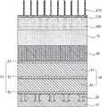
于基底10上形成第一支撑结构30和牺牲层40。第一支撑结构30、牺牲层40层叠设置。第一支撑结构30和牺牲层40的层数为多层,且第一支撑结构30和牺牲层40依次交替层叠设置。A
其中,第一支撑结构30和牺牲层40的形成过程可以采用以下方法:Wherein, the formation process of the
利用原子层沉积工艺、物理气相沉积工艺或化学气相沉积工艺在基底10上依次形成层叠设置的第一初始支撑层31、第一牺牲层41、第二初始支撑层32、第二牺牲层42和第三初始支撑层33。A first
也就是说,在该实施例中,第一支撑结构30的层数为间隔设置的三层,牺牲层40的层数为间隔设置的两层。其中,第一支撑结构30的材料可以包括但不限于氮化硅或碳氮化硅,牺牲层40的材料可以包括但不限于氧化物或多晶硅。That is to say, in this embodiment, the number of layers of the
本实施例中,通过上述第一支撑结构和牺牲层的结构设计,可以对后续所形成的介电层和第一电极结构进行侧壁支撑,防止介电层和第一电极结构在后续工艺中倾斜或倒塌。而牺牲层40可以在后续形成第二电极结构时去除。In this embodiment, through the structural design of the first support structure and the sacrificial layer, the sidewall support of the subsequently formed dielectric layer and the first electrode structure can be performed to prevent the dielectric layer and the first electrode structure from being damaged in the subsequent process. Tilt or collapse. The
根据一个示例性实施例,本实施例是对上文中步骤S300的进一步说明。According to an exemplary embodiment, this embodiment is a further description of the above step S300.
如图13所示,于位于顶层的第一支撑结构30上形成多个第一通孔50,其中,多个第一通孔50与多个分立设置的接触结构20一一对应设置,并且,每个第一通孔50依次贯穿第三初始支撑层33、第二牺牲层42、第二初始支撑层32、第一牺牲层41和第一初始支撑层31,并暴露出位于第一通孔50下方的接触结构20的顶面。As shown in FIG. 13 , a plurality of first through
在一些实施例中,如图2至图13所示,第一通孔50的形成过程可以采用以下方法:In some embodiments, as shown in FIG. 2 to FIG. 13 , the formation process of the first through
利用原子层沉积工艺、物理气相沉积工艺或化学气相沉积工艺在顶层的第一支撑结构30(具体为第三初始支撑层33)上形成层叠设置的第二介质层60和第三牺牲层70。其中,第二介质层60的材质可以包括但不限于多晶硅。第三牺牲层70的材质可以包括但不限于氧化物,比如氧化硅等。The
而后,图形化第三牺牲层70,以在第三牺牲层70上形成多个间隔设置的第五通孔80。其中,多个第五通孔80与多个分立设置的接触结构20一一对应设置。Then, the third
沿第五通孔80,利用刻蚀工艺对第二介质层60进行刻蚀处理,以在第二介质层60内形成多个间隔设置的第六通孔90。多个第六通孔90与多个第五通孔80一一对应设置。Along the fifth through
然后,通过刻蚀气体或刻蚀液去除剩余的第三牺牲层70。Then, the remaining third
待第三牺牲层70去除完成后,沿第六通孔90利用刻蚀工艺对第一支撑结构30进行刻蚀处理,以在第一支撑结构30上形成多个间隔设置的第一通孔50。After the third
最后,利用刻蚀气体或刻蚀液去除剩余的第二介质层60。Finally, the remaining
在本实施例中,利用层叠设置的第二介质层60和第三牺牲层70,经过多次刻蚀依次形成第五通孔80和第六通孔90,最后沿第六通孔90刻蚀形成第一通孔50,能够有效增加第一通孔50的刻蚀精度,以及获得高深宽比的第一通孔50,提高了后续形成的电容结构的器件性能和半导体结构的良率。In this embodiment, the
如图10至图11所示,在一些实施例中,形成上文中第五通孔80的过程可以采用以下方法:As shown in FIG. 10 to FIG. 11 , in some embodiments, the process of forming the fifth through
利用原子层沉积工艺、物理气相沉积工艺或化学气相沉积工艺在第三牺牲层70上沉积层叠设置的第三介质层100和第一隔离层110。其中,第三介质层100可以包括旋涂碳层,第一隔离层110的材料可以包括但不限于氮氧化硅。The stacked third
而后,图形化第三介质层100和第一隔离层110,以在第一隔离层110和第三介质层100内形成第七通孔120。Then, the third
然后,沿第七通孔120利用刻蚀工艺对第三牺牲层70进行刻蚀处理,从而形成间隔设置的多个第五通孔80。Then, the third
待第五通孔80形成之后,去除剩余的第三介质层100和第一隔离层110。After the fifth through
本实施例中,通过在第三介质层100和第一隔离层110中形成第七通孔120,而后形成第五通孔80,能够有效提高第五通孔80的刻蚀质量,从而保证后续所形成的第一通孔50的形成质量。In this embodiment, by forming the seventh through
参照图2至图10所示,为了提高第七通孔120的形成质量,保证所形成的第一通孔50的形状质量,并有效提高半导体结构的性能和良率。在一些实施例中,第七通孔120的形成过程可以采用以下方法:Referring to FIG. 2 to FIG. 10 , in order to improve the formation quality of the seventh through
利用原子层沉积工艺、物理气相沉积工艺或化学沉积工艺在第一隔离层110上依次沉积形成层叠设置的第一旋涂碳层130和第一氮氧化硅层140。A first spin-on
待第一氮氧化硅层140形成之后,在第一氮氧化硅层140顶面上形成一层第一光刻胶层141,图形化第一光刻胶层141,以在第一光刻胶层141上形成多个掩膜开口,以掩膜开口为基准,利用刻蚀工艺在第一旋涂碳层130和第一氮氧化硅层140上形成多个间隔设置第八通孔150。After the first
而后,利用原子层沉积工艺、化学气相沉积工艺或物理气相沉积工艺在第八通孔150内形成第一掩膜层160。第一掩膜层160延伸至第八通孔150外并覆盖第一氮氧化硅层140的顶面。Then, a
通过刻蚀工艺去除部分第一掩膜层160,保留位于第八通孔150侧壁上的第一掩膜层160,被保留下来的第一掩膜层160形成第一掩膜柱170。A part of the
利用刻蚀工艺去除剩余的第一旋涂碳层130和第一氮氧化硅层140,保留第一掩膜柱170。The remaining first spin-on
然后,在第一隔离层110上形成第二旋涂碳层180、第二氮氧化硅层190、第三旋涂碳层200和第三氮氧化硅层210。其中,第二旋涂碳层180覆盖多个第一掩膜柱170。Then, a second spin-on
利用刻蚀工艺在第三氮氧化硅层210和第三旋涂碳层200中形成多个间隔设置的第九通孔220。利用沉积工艺在第九通孔220内形成第二掩膜层230,第二掩膜层230延伸至第九通孔220外并覆盖第三氮氧化硅层210的顶面。A plurality of ninth through
通过刻蚀工艺去除部分第二掩膜层230,保留位于第九通孔220侧壁上的第二掩膜层230,被保留下来的第二掩膜层230形成第二掩膜柱240。其中,第二掩膜柱240和第一掩膜柱170错位设置。A part of the
最后,以第一掩膜柱170和第二掩膜柱240为掩膜利用刻蚀工艺对第一隔离层110和第三介质层100进行刻蚀处理,从而形成多个间隔设置的第七通孔120。Finally, the
根据一个示例性实施例,本实施例是对上文中步骤S400的进一步说明。According to an exemplary embodiment, this embodiment is a further description of the above step S400.
如图13至图23所示,在一些实施例中,介电层250的形成过程可以采用以下方法:As shown in FIG. 13 to FIG. 23 , in some embodiments, the formation process of the
利用原子层沉积工艺、化学气相沉积工艺或物理气相沉积工艺在第一通孔50内形成初始介电层251,初始介电层251延伸至第一通孔50外,并覆盖第一支撑结构30的部分顶面,即,上层第一支撑结构30的顶面。其中,初始介电层251的材料可以包括但不限于高K材料。An
而后,通过刻蚀工艺去除位于第一通孔50底部的初始介电层251,被保留下来的初始介电层251形成中间介电层252,此时,第一通孔50内的中间介电层252之间形成第二通孔260。Then, the
然后,再通过刻蚀工艺去除相邻的第一通孔50之间的第一支撑结构30的顶面的部分中间介电层252,被保留下来的中间介电层252形成介电层250。Then, part of the
参照图13至图26所示,在一些实施例中,相邻的第一通孔50之间的第一支撑结构30顶面的中间介电层252可以全部去除;或者,去除一部分中间介电层252,保留靠近第一通孔50的部分中间介电层252,该部分中间介电层252的侧壁与位于其下方的第一支撑结构30的外侧壁平齐;又或者,去除一部分中间介电层252,被保留下来的部分中间介电层252的长度为位于其下方的第一支撑结构30的顶面的长度的三分之一至二分之一。Referring to FIGS. 13 to 26 , in some embodiments, the
需要说明的是,在一些实施例中,介电层250可以为叠层结构,例如,介电层250可以包括三层结构,且三层结构的材质分别为氧化锆-氧化铝-氧化锆,即,介电层250可以包括依次连接的氧化锆层、氧化铝层和氧化锆层。It should be noted that, in some embodiments, the
本实施例中,先形成初始介电层,而后去除第一通孔的底壁的初始介电层以形成中间介电层,最后再将相邻第一通孔之间的支撑结构顶面的部分中间介电层去除,形成介电层,上述形成介电层的过程的方法简单,且便于操作,能有效保证介电层的形成质量和形成厚度,从而提高半导体结构的性能和良率。In this embodiment, an initial dielectric layer is formed first, and then the initial dielectric layer on the bottom wall of the first through hole is removed to form an intermediate dielectric layer, and finally the top surface of the support structure between adjacent first through holes is removed. Part of the intermediate dielectric layer is removed to form a dielectric layer. The above-mentioned method of forming the dielectric layer is simple and easy to operate, and can effectively ensure the formation quality and thickness of the dielectric layer, thereby improving the performance and yield of the semiconductor structure.
根据一个示例性实施例,本实施例是对上文中步骤S500的进一步说明。According to an exemplary embodiment, this embodiment is a further description of the above step S500.
如图15至图20所示,在第二通孔260内形成第一电极结构270。其中,第一电极结构270包括第一电极层271和缓冲层272,第一电极层271可以包括电容结构中的下电极,且第一电极层271的材料可以包括但不限于钨、多晶硅或氮化钛等。缓冲层272的材料可以包括但不限于多晶硅、掺杂碳的氮化硅或掺杂碳的氧化硅中的一种或多种,或者,其他低应力材料。As shown in FIGS. 15 to 20 , a
在一些实施例中,第一电极结构270的形成可以采用以下方法:In some embodiments, the formation of the
首先,利用原子层沉积工艺、化学气相沉积工艺或物理气相沉积工艺在第二通孔260的侧壁和底部形成第一电极层271。第二通孔260内的第一电极层271之间形成第三通孔280。First, the
本实施例中,第一电极层271的形成过程包括:In this embodiment, the formation process of the
利用沉积工艺在第二通孔260内形成第一初始电极层2711,第一初始电极层2711延伸至第二通孔260外,并覆盖介电层250的顶面。A first
而后,将位于介电层250的顶面的部分第一初始电极层2711断开,被保留下来的第一初始电极层2711形成第一电极层271。Then, part of the first
其中,第一初始电极层2711的断开过程可以包括:The disconnection process of the first
利用沉积工艺在第一初始电极层2711上形成依次层叠设置的第一介质层290、隔离层300和掩膜层310。A first dielectric layer 290 , an
图形化掩膜层310,以在掩膜层310上形成掩膜开口。通过掩膜开口刻蚀去除部分隔离层300、部分第一介质层290和部分第一初始电极层2711。最后通过刻蚀工艺去除剩余的掩膜层310、隔离层300和第一介质层290,从而将介电层250顶面的部分第一初始电极层2711断开。The
本实施例中,利用第一介质层、隔离层和掩膜层,能够准确去除部分第一初始电极层,提高后续保留下来的第一电极层的形成精度。In this embodiment, by using the first dielectric layer, the isolation layer and the mask layer, part of the first initial electrode layer can be accurately removed, and the formation accuracy of the subsequently retained first electrode layer can be improved.
待第一电极层271形成之后,通过沉积工艺在第三通孔280内沉积一层初始缓冲层2721,该初始缓冲层2721延伸至第三通孔280外,并覆盖中间介电层252的顶面上。待初始缓冲层2721形成之后,通过刻蚀或化学机械研磨去除中间介电层250的顶面的初始缓冲层2721,保留位于第三通孔280内的初始缓冲层2721,被保留下来的初始缓冲层2721形成缓冲层272。缓冲层272和第一电极层271形成第一电极结构270。该第一电极结构270形成之后覆盖部分接触结构20的表面以及位于第二通孔260内的介电层250的侧壁上,每个第一电极结构270对应不同的接触结构20。After the
本实施例中,第一电极结构包括第一电极层和缓冲层,并且第一电极层包裹缓冲层,从而通过缓冲层减少后续电容结构在形成过程中的应力,提高电容结构的稳定性。In this embodiment, the first electrode structure includes a first electrode layer and a buffer layer, and the first electrode layer wraps the buffer layer, so that the buffer layer reduces the stress during the formation of the subsequent capacitor structure and improves the stability of the capacitor structure.
根据一个示例性实施例,本实施例是对上文中步骤S600的进一步说明。According to an exemplary embodiment, this embodiment is a further description of the above step S600.
如图21至图23所示,待第一电极结构270形成之后,在第一电极结构270上形成第二支撑结构320。其中,第二支撑结构320的材料包括但不限于氮化硅或硅碳氮,且第二支撑结构320可以为单层结构,也可以为层叠设置的多层结构。As shown in FIGS. 21 to 23 , after the
以第二支撑结构320为单层结构为例,可以利用原子层沉积工艺、物理气相沉积工艺或化学气相沉积工艺在介电层250的顶面上形成第二支撑结构320。Taking the
根据一个示例性实施例,本实施例是对上文中步骤S700的进一步说明。According to an exemplary embodiment, this embodiment is a further description of step S700 above.
继续参照图21至图23所示,在一些实施例中,将第一电极结构270断开的过程可以通过去除牺牲层40、部分第一支撑结构30和部分第二支撑结构320的方式来实现,具体过程如下:Continuing to refer to FIGS. 21 to 23 , in some embodiments, the process of disconnecting the
通过沉积工艺在第二支撑结构320上形成依次层叠设置的第四旋涂碳层321、第四氮氧化硅层322和第四掩膜层323。A fourth spin-on
图形化第四掩膜层323,从而在第四掩膜层323上形成掩膜开口。而后,利用掩膜开口对第四氮氧化硅层322、第四旋涂碳层321和第二支撑结构320上进行刻蚀,以在第二支撑结构320上形成多个分立设置的第四通孔330,并通过刻蚀工艺去除剩余的第四旋涂碳层321、第四氮氧化硅层322和第四掩膜层323。The
然后,继续刻蚀,直至第四通孔330依次贯穿第二支撑结构320、中间介电层252、第一支撑结构30和牺牲层40。Then, the etching is continued until the fourth through
待第四通孔330形成之后,利用第四通孔330所形成的开口区域,通过刻蚀工艺去除剩余的牺牲层40(包括第一牺牲层41和第二牺牲层42),以暴露介电层250的部分侧壁,被保留下来的第一支撑结构30和第二支撑结构320形成支撑结构340。After the fourth through
在本实施例中,利用第四通孔一方面可以将中间介电层断开,另一方面也便于去除牺牲层,从而方便后续形成第二电极结构。In this embodiment, on the one hand, the intermediate dielectric layer can be disconnected by using the fourth through hole, and on the other hand, it is convenient to remove the sacrificial layer, so as to facilitate the subsequent formation of the second electrode structure.
根据一个示例性实施例,本实施例是对上文中步骤S800的进一步说明。According to an exemplary embodiment, this embodiment is a further description of step S800 above.
如图24所示,待支撑结构340形成之后,形成第二电极结构350,第二电极结构350可以包括电容结构中的上电极,第二电极结构350的材料可以包括但不限于多晶硅、钨或氮化钛等。其中,在一些实施例中,第二电极结构350的形成过程可以采用以下方法:As shown in FIG. 24 , after the supporting
利用原子层沉积工艺、物理气相沉积工艺或化学气相沉积工艺形成第二电极结构350,该第二电极结构350包裹支撑结构340和介电层250的部分侧壁。The
其中,在一些公开示例中,可以通过原子层沉积工艺于支撑结构340和介电层250的部分侧壁上形成第二电极结构350。原子层沉积工艺具有沉积速率慢、沉积形成的膜层致密性高以及阶梯覆盖率好的特点。利用原子层沉积工艺形成第二电极结构能够在空间范围较小的条件下对支撑结构和介电层的侧壁进行覆盖,避免占据较大的空间,有效保证第二电极结构的形成质量,进而提高后续所形成的电容结构的性能和良率。Wherein, in some disclosed examples, the
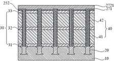
如图24至图26所示,本公开一示例性的实施例提供了一种半导体结构。该半导体结构包括:基底10、第一电极结构270、介电层250、第一支撑结构30、第二支撑结构320和第二电极结构350。As shown in FIGS. 24-26 , an exemplary embodiment of the present disclosure provides a semiconductor structure. The semiconductor structure includes: a
其中,在基底10内设有多个分立设置的接触结构20。第一电极结构270设在基底10上,并与接触结构20连接,多个第一电极结构270与多个接触结构20一一对应设置,即,每个第一电极结构270对应不同的接触结构20。介电层250设在第一电极结构270的外侧壁上。Wherein, a plurality of
第一支撑结构30设置在介电层250两侧的侧壁上,并且,介电层250还覆盖第一支撑结构30的部分顶面。第二支撑结构320设在介电层250的顶面上。第二电极结构350覆盖第一支撑结构30、第二支撑结构320和介电层250的外表面。The
在本实施例中,第一电极结构、介电层和第二电极结构共同构成一种电容结构。而在该电容结构的形成过程中,先形成介电层,在保证介电层的填充能力和填充质量的前提下,再形成第一电极结构和第二电极结构,从而有效提高了后续所形成的第一电极结构和第二电极结构之间的绝缘性,防止第一电极结构和第二电极结构之间发生漏电,从而提高了半导体结构的性能和良率。In this embodiment, the first electrode structure, the dielectric layer and the second electrode structure together constitute a capacitor structure. In the process of forming the capacitor structure, the dielectric layer is formed first, and the first electrode structure and the second electrode structure are formed on the premise of ensuring the filling ability and filling quality of the dielectric layer, thereby effectively improving the subsequent formation The insulation between the first electrode structure and the second electrode structure prevents leakage between the first electrode structure and the second electrode structure, thereby improving the performance and yield of the semiconductor structure.
如图25所示,在一些实施例中,介电层250包括第一介电层253和第二介电层254。其中,第一介电层253设在第一电极结构270的外侧壁上,第一介电层253沿自基底10的底面至其顶面的延伸方向设置。第二介电层254位于第一支撑结构30和第二支撑结构320之间,第二介电层254的一端与第一介电层253的顶端连接,且第二介电层254覆盖整个第一支撑结构30的顶面。As shown in FIG. 25 , in some embodiments, the
本实施例中,第二介电层的外侧壁与第一支撑结构和第二支撑结构的外侧壁平齐设置,能够减少半导体结构的制程工序,有助于提高半导体结构的产能,另一个方面,第二介电层也能提高第一电极结构和第二电极结构之间的绝缘效果,提高半导体结构的性能和良率。In this embodiment, the outer sidewalls of the second dielectric layer are disposed flush with the outer sidewalls of the first support structure and the second support structure, which can reduce the manufacturing process of the semiconductor structure and help improve the productivity of the semiconductor structure. On the other hand, , the second dielectric layer can also improve the insulating effect between the first electrode structure and the second electrode structure, and improve the performance and yield of the semiconductor structure.
如图26所示,在一些实施例中,介电层250包括第三介电层255。第三介电层255设在第一电极结构270的外侧壁上,并沿自基底10的底面至其顶面的延伸方向设置。其中,第三介电层255的顶面与第一电极结构270的顶面平齐。As shown in FIG. 26 , in some embodiments, the
本实施例中,第三介电层的顶面与第一电极结构的顶面平齐,由此,可以在同一刻蚀步骤中去除部分第三介电层和部分第一电极结构,减少半导体结构的制程工序,从而提高半导体结构的产能。In this embodiment, the top surface of the third dielectric layer is flush with the top surface of the first electrode structure, so that part of the third dielectric layer and part of the first electrode structure can be removed in the same etching step, reducing the number of semiconductors The manufacturing process of the structure, thereby increasing the productivity of the semiconductor structure.
如图24所示,在一些实施例中,介电层250包括第四介电层256和第五介电层257。第四介电层256设在第一电极结构270的外侧壁上,并沿自基底10的底面至其顶面的方向延伸。第五介电层257位于第一支撑结构30和第二支撑结构320之间,第五介电层257的一端与第四介电层256的顶端连接,其中,第五介电层257覆盖部分第一支撑结构30的顶面。As shown in FIG. 24 , in some embodiments, the
在一些公开实施例中,第五介电层257可以覆盖第一支撑结构30的顶面的三分之一至二分之一之间。In some disclosed embodiments, the
本实施例中,第五介电层覆盖部分第一支撑结构的顶面,且第五介电层的长度与第一支撑结构的顶面的长度之间可以存在比例关系,从而可以使得后续形成不同规格的电容结构,提高了半导体结构的适用性。In this embodiment, the fifth dielectric layer covers part of the top surface of the first support structure, and there may be a proportional relationship between the length of the fifth dielectric layer and the length of the top surface of the first support structure, so that the subsequent formation of Capacitor structures of different specifications improve the applicability of semiconductor structures.
如图24至图26所示,在一些实施例中,第一电极结构270包括第一电极层271和缓冲层272。第一电极层271与接触结构20连接,并包裹缓冲层272。其中,第一电极层271的外侧壁与介电层250连接。其中,缓冲层272的材质可以包括但不限于多晶硅、掺杂碳的氮化硅或掺杂碳的氧化硅中的一种或多种。或者,缓冲层272的材质还可以是其他低应力的材料。As shown in FIGS. 24 to 26 , in some embodiments, the
本实施例中,第一电极层包裹缓冲层设置,而缓冲层可以减少后续电容结构在形成过程中的应力,提高电容结构的稳定性。In this embodiment, the first electrode layer is arranged by wrapping the buffer layer, and the buffer layer can reduce the stress during the formation of the subsequent capacitor structure and improve the stability of the capacitor structure.
在本公开的描述中,需要说明的是,术语“中心”、“上”、“下”、“左”、“右”、“竖直”、“水平”、“内”、“外”等指示的方位或位置关系为基于附图所示的方位或位置关系,仅是为了便于描述本公开和简化描述,而不是指示或暗示所指的装置或元件必须具有特定的方位、以特定的方位构造和操作,因此不能理解为对本公开的限制。In the description of the present disclosure, it should be noted that the terms "center", "upper", "lower", "left", "right", "vertical", "horizontal", "inner", "outer", etc. The indicated orientation or positional relationship is based on the orientation or positional relationship shown in the drawings, and is only for the convenience of describing the present disclosure and simplifying the description, rather than indicating or implying that the indicated device or element must have a specific orientation or a specific orientation. construction and operation, and therefore should not be construed as limiting the present disclosure.
可以理解的是,本公开所使用的术语“第一”、“第二”等可在本公开中用于描述各种结构,但这些结构不受这些术语的限制。这些术语仅用于将第一个结构与另一个结构区分。It will be understood that the terms "first", "second", etc. used in the present disclosure may be used in the present disclosure to describe various structures, but these structures are not limited by these terms. These terms are only used to distinguish one structure from another.
在一个或多个附图中,相同的元件采用类似的附图标记来表示。为了清楚起见,附图中的多个部分没有按比例绘制。此外,可能未示出某些公知的部分。为了简明起见,可以在一幅图中描述经过数个步骤后获得的结构。在下文中描述了本公开的许多特定的细节,例如器件的结构、材料、尺寸、处理工艺和技术,以便更清楚地理解本公开。但正如本领域技术人员能够理解的那样,可以不按照这些特定的细节来实现本公开。Like elements are represented by like reference numerals in one or more of the figures. For the sake of clarity, various parts of the figures are not drawn to scale. Additionally, some well-known parts may not be shown. For the sake of brevity, the structure obtained after several steps can be depicted in one figure. Numerous specific details of the present disclosure are described below, such as device structures, materials, dimensions, processing techniques and techniques, in order to provide a clearer understanding of the present disclosure. However, as can be understood by one skilled in the art, the present disclosure may be practiced without these specific details.
最后应说明的是:以上各实施例仅用以说明本公开的技术方案,而非对其限制;尽管参照前述各实施例对本公开进行了详细的说明,本领域技术人员应当理解:其依然可以对前述各实施例所记载的技术方案进行修改,或者对其中部分或者全部技术特征进行等同替换;而这些修改或者替换,并不使相应技术方案的本质脱离本公开各实施例技术方案的范围。Finally, it should be noted that the above embodiments are only used to illustrate the technical solutions of the present disclosure, but not to limit them; although the present disclosure has been described in detail with reference to the above-mentioned embodiments, those skilled in the art should understand that: it can still be Modifications are made to the technical solutions described in the foregoing embodiments, or some or all of the technical features thereof are equivalently replaced; these modifications or replacements do not make the essence of the corresponding technical solutions depart from the scope of the technical solutions of the embodiments of the present disclosure.
Claims (17)
Priority Applications (1)
| Application Number | Priority Date | Filing Date | Title |
|---|---|---|---|
| CN202210462531.7ACN114582958B (en) | 2022-04-29 | 2022-04-29 | Manufacturing method of semiconductor structure and semiconductor structure |
Applications Claiming Priority (1)
| Application Number | Priority Date | Filing Date | Title |
|---|---|---|---|
| CN202210462531.7ACN114582958B (en) | 2022-04-29 | 2022-04-29 | Manufacturing method of semiconductor structure and semiconductor structure |
Publications (2)
| Publication Number | Publication Date |
|---|---|
| CN114582958A CN114582958A (en) | 2022-06-03 |
| CN114582958Btrue CN114582958B (en) | 2022-08-02 |
Family
ID=81784782
Family Applications (1)
| Application Number | Title | Priority Date | Filing Date |
|---|---|---|---|
| CN202210462531.7AActiveCN114582958B (en) | 2022-04-29 | 2022-04-29 | Manufacturing method of semiconductor structure and semiconductor structure |
Country Status (1)
| Country | Link |
|---|---|
| CN (1) | CN114582958B (en) |
Families Citing this family (2)
| Publication number | Priority date | Publication date | Assignee | Title |
|---|---|---|---|---|
| CN118042824A (en)* | 2022-11-04 | 2024-05-14 | 长鑫存储技术有限公司 | Semiconductor structure and manufacturing method thereof |
| CN115939031A (en)* | 2022-12-30 | 2023-04-07 | 联合微电子中心有限责任公司 | Wafer structure and method for controlling wafer bow |
Citations (6)
| Publication number | Priority date | Publication date | Assignee | Title |
|---|---|---|---|---|
| CN107706181A (en)* | 2017-10-27 | 2018-02-16 | 睿力集成电路有限公司 | High aspect ratio structure, capacitor arrangement, semiconductor storage unit and preparation method |
| CN110504283A (en)* | 2018-05-17 | 2019-11-26 | 长鑫存储技术有限公司 | Columnar capacitor array structure and preparation method |
| CN111106095A (en)* | 2018-10-29 | 2020-05-05 | 长鑫存储技术有限公司 | Trenches and methods for forming the same, methods for making capacitors, and capacitors |
| CN111328428A (en)* | 2020-02-10 | 2020-06-23 | 长江存储科技有限责任公司 | Semiconductor plug having etch-resistant layer in three-dimensional memory device |
| CN113161484A (en)* | 2021-04-19 | 2021-07-23 | 长鑫存储技术有限公司 | Preparation method of semiconductor structure and semiconductor structure |
| CN113314669A (en)* | 2020-02-27 | 2021-08-27 | 长鑫存储技术有限公司 | Double-sided capacitor structure and forming method thereof |
Family Cites Families (1)
| Publication number | Priority date | Publication date | Assignee | Title |
|---|---|---|---|---|
| US11869932B2 (en)* | 2020-09-10 | 2024-01-09 | Changxin Memory Technologies, Inc. | Manufacturing method of capacitive structure, and capacitor |
- 2022
- 2022-04-29CNCN202210462531.7Apatent/CN114582958B/enactiveActive
Patent Citations (6)
| Publication number | Priority date | Publication date | Assignee | Title |
|---|---|---|---|---|
| CN107706181A (en)* | 2017-10-27 | 2018-02-16 | 睿力集成电路有限公司 | High aspect ratio structure, capacitor arrangement, semiconductor storage unit and preparation method |
| CN110504283A (en)* | 2018-05-17 | 2019-11-26 | 长鑫存储技术有限公司 | Columnar capacitor array structure and preparation method |
| CN111106095A (en)* | 2018-10-29 | 2020-05-05 | 长鑫存储技术有限公司 | Trenches and methods for forming the same, methods for making capacitors, and capacitors |
| CN111328428A (en)* | 2020-02-10 | 2020-06-23 | 长江存储科技有限责任公司 | Semiconductor plug having etch-resistant layer in three-dimensional memory device |
| CN113314669A (en)* | 2020-02-27 | 2021-08-27 | 长鑫存储技术有限公司 | Double-sided capacitor structure and forming method thereof |
| CN113161484A (en)* | 2021-04-19 | 2021-07-23 | 长鑫存储技术有限公司 | Preparation method of semiconductor structure and semiconductor structure |
Also Published As
| Publication number | Publication date |
|---|---|
| CN114582958A (en) | 2022-06-03 |
Similar Documents
| Publication | Publication Date | Title |
|---|---|---|
| US8058678B2 (en) | Semiconductor memory device including a cylinder type storage node and a method of fabricating the same | |
| CN102646638B (en) | Comprise semiconductor device and the manufacture method thereof of capacitor and Metal Contact | |
| CN100405541C (en) | Capacitor capacitor and method of forming same | |
| CN113345835B (en) | Semiconductor device and method for manufacturing the same | |
| US8841195B2 (en) | Semiconductor device with multi-layered storage node and method for fabricating the same | |
| TWI440140B (en) | Memory capacitor structure and manufacturing method thereof | |
| CN100405589C (en) | Semiconductor device and manufacturing method thereof | |
| JP2010226109A (en) | Capacitor structure and manufacturing method thereof, and semiconductor device including the capacitor and manufacturing method thereof | |
| WO2021109595A1 (en) | Memory and forming method therefor | |
| US20230171947A1 (en) | Semiconductor structure and manufacturing method thereof | |
| JP2009164535A (en) | Semiconductor device and manufacturing method thereof | |
| CN112951770B (en) | Storage method and storage method | |
| CN114582958B (en) | Manufacturing method of semiconductor structure and semiconductor structure | |
| KR100632938B1 (en) | DRAM device having capacitor and method for forming same | |
| CN113314669A (en) | Double-sided capacitor structure and forming method thereof | |
| WO2022205711A1 (en) | Method for preparing semiconductor structure and semiconductor structure | |
| CN114639638B (en) | Manufacturing method of semiconductor structure and semiconductor structure | |
| JP2010153509A (en) | Semiconductor device and manufacturing method thereof | |
| KR20050116421A (en) | Method of forming self-aligned contact in semiconductor memory device and method of fabricating the semiconductor memory device using the method | |
| TW202329398A (en) | Semiconductor structure and manufacturing method thereof | |
| US6844229B2 (en) | Method of manufacturing semiconductor device having storage electrode of capacitor | |
| US20100155802A1 (en) | Semiconductor device and method of forming semiconductor device | |
| KR100949880B1 (en) | Semiconductor device and manufacturing method thereof | |
| CN111370419A (en) | A semiconductor device and method of making the same | |
| JPH09331038A (en) | Semiconductor memory and its fabrication |
Legal Events
| Date | Code | Title | Description |
|---|---|---|---|
| PB01 | Publication | ||
| PB01 | Publication | ||
| SE01 | Entry into force of request for substantive examination | ||
| SE01 | Entry into force of request for substantive examination | ||
| GR01 | Patent grant | ||
| GR01 | Patent grant |