CN114551627A - light sensing module - Google Patents
light sensing moduleDownload PDFInfo
- Publication number
- CN114551627A CN114551627ACN202011255911.0ACN202011255911ACN114551627ACN 114551627 ACN114551627 ACN 114551627ACN 202011255911 ACN202011255911 ACN 202011255911ACN 114551627 ACN114551627 ACN 114551627A
- Authority
- CN
- China
- Prior art keywords
- light
- sensing module
- light sensing
- wavelength conversion
- conversion structure
- Prior art date
- Legal status (The legal status is an assumption and is not a legal conclusion. Google has not performed a legal analysis and makes no representation as to the accuracy of the status listed.)
- Granted
Links
- 238000006243chemical reactionMethods0.000claimsabstractdescription78
- 239000000126substanceSubstances0.000claimsdescription52
- 239000000843powderSubstances0.000claimsdescription36
- 239000000945fillerSubstances0.000claimsdescription34
- 230000003287optical effectEffects0.000claimsdescription26
- VYPSYNLAJGMNEJ-UHFFFAOYSA-NSilicium dioxideChemical compoundO=[Si]=OVYPSYNLAJGMNEJ-UHFFFAOYSA-N0.000claimsdescription25
- 239000000463materialSubstances0.000claimsdescription25
- -1methyl silica gelChemical compound0.000claimsdescription22
- 229910002027silica gelInorganic materials0.000claimsdescription21
- 239000000741silica gelSubstances0.000claimsdescription21
- 229910052761rare earth metalInorganic materials0.000claimsdescription13
- 229910052751metalInorganic materials0.000claimsdescription10
- 239000002184metalSubstances0.000claimsdescription10
- 238000001228spectrumMethods0.000claimsdescription10
- 239000000377silicon dioxideSubstances0.000claimsdescription9
- GWEVSGVZZGPLCZ-UHFFFAOYSA-NTitan oxideChemical compoundO=[Ti]=OGWEVSGVZZGPLCZ-UHFFFAOYSA-N0.000claimsdescription8
- 229920001343polytetrafluoroethylenePolymers0.000claimsdescription5
- 239000004810polytetrafluoroethyleneSubstances0.000claimsdescription5
- XLOMVQKBTHCTTD-UHFFFAOYSA-NZinc monoxideChemical compound[Zn]=OXLOMVQKBTHCTTD-UHFFFAOYSA-N0.000claimsdescription4
- 239000000853adhesiveSubstances0.000claimsdescription4
- 230000001070adhesive effectEffects0.000claimsdescription4
- 238000005538encapsulationMethods0.000claimsdescription4
- 229910044991metal oxideInorganic materials0.000claimsdescription4
- 150000004706metal oxidesChemical class0.000claimsdescription4
- 239000004408titanium dioxideSubstances0.000claimsdescription4
- 229920001296polysiloxanePolymers0.000claimsdescription3
- 235000012239silicon dioxideNutrition0.000claimsdescription3
- 229910052582BNInorganic materials0.000claimsdescription2
- PZNSFCLAULLKQX-UHFFFAOYSA-NBoron nitrideChemical compoundN#BPZNSFCLAULLKQX-UHFFFAOYSA-N0.000claimsdescription2
- MCMNRKCIXSYSNV-UHFFFAOYSA-NZrO2Inorganic materialsO=[Zr]=OMCMNRKCIXSYSNV-UHFFFAOYSA-N0.000claimsdescription2
- PMHQVHHXPFUNSP-UHFFFAOYSA-Mcopper(1+);methylsulfanylmethane;bromideChemical compoundBr[Cu].CSCPMHQVHHXPFUNSP-UHFFFAOYSA-M0.000claimsdescription2
- 150000004767nitridesChemical class0.000claimsdescription2
- TWNQGVIAIRXVLR-UHFFFAOYSA-Noxo(oxoalumanyloxy)alumaneChemical compoundO=[Al]O[Al]=OTWNQGVIAIRXVLR-UHFFFAOYSA-N0.000claimsdescription2
- RVTZCBVAJQQJTK-UHFFFAOYSA-Noxygen(2-);zirconium(4+)Chemical compound[O-2].[O-2].[Zr+4]RVTZCBVAJQQJTK-UHFFFAOYSA-N0.000claimsdescription2
- 229910052814silicon oxideInorganic materials0.000claimsdescription2
- 239000011787zinc oxideSubstances0.000claimsdescription2
- OAICVXFJPJFONN-UHFFFAOYSA-NPhosphorusChemical compound[P]OAICVXFJPJFONN-UHFFFAOYSA-N0.000claims1
- 125000001153fluoro groupChemical groupF*0.000claims1
- LIVNPJMFVYWSIS-UHFFFAOYSA-Nsilicon monoxideChemical class[Si-]#[O+]LIVNPJMFVYWSIS-UHFFFAOYSA-N0.000claims1
- 230000035945sensitivityEffects0.000description28
- 229920002050silicone resinPolymers0.000description24
- 239000008393encapsulating agentSubstances0.000description23
- 230000000694effectsEffects0.000description15
- 230000000052comparative effectEffects0.000description9
- 239000000919ceramicSubstances0.000description7
- 229910052712strontiumInorganic materials0.000description4
- 229910052788bariumInorganic materials0.000description2
- 230000009286beneficial effectEffects0.000description2
- 229910052791calciumInorganic materials0.000description2
- 238000002474experimental methodMethods0.000description2
- 125000000524functional groupChemical group0.000description2
- 125000001997phenyl groupChemical group[H]C1=C([H])C([H])=C(*)C([H])=C1[H]0.000description2
- 102100032047AlsinHuman genes0.000description1
- 101710187109AlsinProteins0.000description1
- 229910004283SiO 4Inorganic materials0.000description1
- 229910052771TerbiumInorganic materials0.000description1
- 229910052782aluminiumInorganic materials0.000description1
- 230000007812deficiencyEffects0.000description1
- 230000005284excitationEffects0.000description1
- 239000003292glueSubstances0.000description1
- 229910052749magnesiumInorganic materials0.000description1
- 238000000034methodMethods0.000description1
- 125000002496methyl groupChemical group[H]C([H])([H])*0.000description1
- 239000000203mixtureSubstances0.000description1
- 230000035515penetrationEffects0.000description1
- 229920005989resinPolymers0.000description1
- 239000011347resinSubstances0.000description1
- 230000007704transitionEffects0.000description1
Images


Classifications
- H—ELECTRICITY
- H10—SEMICONDUCTOR DEVICES; ELECTRIC SOLID-STATE DEVICES NOT OTHERWISE PROVIDED FOR
- H10F—INORGANIC SEMICONDUCTOR DEVICES SENSITIVE TO INFRARED RADIATION, LIGHT, ELECTROMAGNETIC RADIATION OF SHORTER WAVELENGTH OR CORPUSCULAR RADIATION
- H10F30/00—Individual radiation-sensitive semiconductor devices in which radiation controls the flow of current through the devices, e.g. photodetectors
- H10F30/20—Individual radiation-sensitive semiconductor devices in which radiation controls the flow of current through the devices, e.g. photodetectors the devices having potential barriers, e.g. phototransistors
- H10F30/21—Individual radiation-sensitive semiconductor devices in which radiation controls the flow of current through the devices, e.g. photodetectors the devices having potential barriers, e.g. phototransistors the devices being sensitive to infrared, visible or ultraviolet radiation
- H—ELECTRICITY
- H10—SEMICONDUCTOR DEVICES; ELECTRIC SOLID-STATE DEVICES NOT OTHERWISE PROVIDED FOR
- H10F—INORGANIC SEMICONDUCTOR DEVICES SENSITIVE TO INFRARED RADIATION, LIGHT, ELECTROMAGNETIC RADIATION OF SHORTER WAVELENGTH OR CORPUSCULAR RADIATION
- H10F77/00—Constructional details of devices covered by this subclass
- H10F77/40—Optical elements or arrangements
- H10F77/413—Optical elements or arrangements directly associated or integrated with the devices, e.g. back reflectors
- H—ELECTRICITY
- H10—SEMICONDUCTOR DEVICES; ELECTRIC SOLID-STATE DEVICES NOT OTHERWISE PROVIDED FOR
- H10F—INORGANIC SEMICONDUCTOR DEVICES SENSITIVE TO INFRARED RADIATION, LIGHT, ELECTROMAGNETIC RADIATION OF SHORTER WAVELENGTH OR CORPUSCULAR RADIATION
- H10F77/00—Constructional details of devices covered by this subclass
- H10F77/40—Optical elements or arrangements
- H10F77/496—Luminescent members, e.g. fluorescent sheets
- H—ELECTRICITY
- H10—SEMICONDUCTOR DEVICES; ELECTRIC SOLID-STATE DEVICES NOT OTHERWISE PROVIDED FOR
- H10F—INORGANIC SEMICONDUCTOR DEVICES SENSITIVE TO INFRARED RADIATION, LIGHT, ELECTROMAGNETIC RADIATION OF SHORTER WAVELENGTH OR CORPUSCULAR RADIATION
- H10F77/00—Constructional details of devices covered by this subclass
- H10F77/50—Encapsulations or containers
Landscapes
- Light Receiving Elements (AREA)
- Engineering & Computer Science (AREA)
- Microelectronics & Electronic Packaging (AREA)
- Led Device Packages (AREA)
- Photometry And Measurement Of Optical Pulse Characteristics (AREA)
Abstract
Translated fromChinese
Description
Translated fromChinese技术领域technical field
本发明涉及一种光感测模块,特别是涉及一种紫外光感测模块。The present invention relates to a light sensing module, in particular to an ultraviolet light sensing module.
背景技术Background technique
紫外光发光二极管(light-emitting diode,LED)的应用越来越广泛,通常会作为一紫外光光源。为了感测紫外光光源的光强度,紫外光发光二极管一般会搭配一紫外光光电二极管(photodiode,PD)使用。Ultraviolet light-emitting diodes (LEDs) are more and more widely used, and are usually used as an ultraviolet light source. In order to sense the light intensity of the ultraviolet light source, the ultraviolet light emitting diode is generally used with an ultraviolet photodiode (PD).
光电二极管的功能是将接收到的光子(photon)转换成电子(electron),当接收到光线的强度越高时,便会产生强度较高的电流。也就是说,光电二极管可将光讯号转换成电讯号,且产生的电讯号的强度会与接收到的光讯号的强度呈正比。The function of the photodiode is to convert the received photons (photon) into electrons (electron). That is, the photodiode can convert the optical signal into an electrical signal, and the intensity of the generated electrical signal is proportional to the intensity of the received optical signal.
一般来说,紫外光光电二极管的价格高出可见光光电二极管的价格许多,导致紫外光感测模块的价格一直居高不下。为了降低紫外光感测模块的价格,现有技术中,尝试将可见光光电二极管与紫外光发光二极管搭配使用,也就是说,以可见光光电二极管取代紫外光光电二极管。然而,一般的可见光光电二极管对紫外光的灵敏度不佳,而无法产生与紫外光强度对应的电流。Generally speaking, the price of UV photodiodes is much higher than that of visible light photodiodes, so the price of UV light sensing modules has remained high. In order to reduce the price of the ultraviolet light sensing module, in the prior art, an attempt is made to use a visible light photodiode with an ultraviolet light emitting diode, that is, to replace the ultraviolet light photodiode with a visible light photodiode. However, general visible light photodiodes have poor sensitivity to ultraviolet light and cannot generate a current corresponding to the intensity of ultraviolet light.
因此,目前尚无法有效降低紫外光感测模块的价格,并且,如何使可见光光电二极管与紫外光发光二极管搭配使用,已成为该领域所欲解决的重要课题之一。Therefore, the price of the ultraviolet light sensing module cannot be effectively reduced at present, and how to use the visible light photodiode with the ultraviolet light emitting diode has become one of the important issues to be solved in this field.
发明内容SUMMARY OF THE INVENTION
本发明所要解决的技术问题在于,针对现有技术的不足提供一种光感测模块。The technical problem to be solved by the present invention is to provide a light sensing module in view of the deficiencies of the prior art.
为了解决上述的技术问题,本发明所采用的其中一技术方案是提供一种光感测模块。本发明公开一种光感测模块。所述光感测模块是用于接受一第一光束,并产生与所述第一光束的强度相对应的一电流。所述光感测模块包括一载体、一光电二极管芯片以及一光波长转换结构,所述光电二极管芯片设置于所述载体上,所述光波长转换结构设置于所述载体上并覆盖所述光电二极管芯片上。其中,所述第一光束通过所述光波长转换结构而转换成一第二光束,所述光电二极管芯片接收所述第二光束并产生所述电流。In order to solve the above technical problems, one of the technical solutions adopted by the present invention is to provide a light sensing module. The invention discloses a light sensing module. The light sensing module is used for receiving a first light beam and generating a current corresponding to the intensity of the first light beam. The light sensing module includes a carrier, a photodiode chip and a light wavelength conversion structure, the photodiode chip is arranged on the carrier, and the light wavelength conversion structure is arranged on the carrier and covers the photoelectric on the diode chip. The first light beam is converted into a second light beam by the light wavelength conversion structure, and the photodiode chip receives the second light beam and generates the current.
为了解决上述的技术问题,本发明所采用的另外一技术方案是提供一种电子装置。所述电子装置包括一光发射模块以及一光感测模块。所述光发射模块产生一第一光束,所述光感测模块是用于接受所述第一光束并产生与所述第一光束的强度相对应的一电流。所述光感测模块包括一载体、一光电二极管芯片以及一光波长转换结构,所述光电二极管芯片设置于所述载体上,所述光波长转换结构设置于所述载体上并覆盖所述光电二极管芯片上。其中,所述第一光束通过所述光波长转换结构而转换成一第二光束,所述光电二极管芯片接收所述第二光束并产生所述电流。In order to solve the above technical problem, another technical solution adopted by the present invention is to provide an electronic device. The electronic device includes a light emitting module and a light sensing module. The light emitting module generates a first light beam, and the light sensing module is used for receiving the first light beam and generating a current corresponding to the intensity of the first light beam. The light sensing module includes a carrier, a photodiode chip and a light wavelength conversion structure, the photodiode chip is arranged on the carrier, and the light wavelength conversion structure is arranged on the carrier and covers the photoelectric on the diode chip. The first light beam is converted into a second light beam by the light wavelength conversion structure, and the photodiode chip receives the second light beam and generates the current.
本发明的其中一有益效果在于,本发明所提供的光感测模块,其能通过“所述第一光束通过所述光波长转换结构而转换成一第二光束”以及“所述光电二极管芯片接收所述第二光束并产生所述电流”的技术方案,以达到降低光感测模块的成本的效果。One of the beneficial effects of the present invention is that the light sensing module provided by the present invention can be converted into a second light beam by "the first light beam is converted into a second light beam by the light wavelength conversion structure" and "the photodiode chip receives the second light beam and generate the current", so as to achieve the effect of reducing the cost of the light sensing module.
为使能更进一步了解本发明的特征及技术内容,请参阅以下有关本发明的详细说明与附图,然而所提供的附图仅用于提供参考与说明,并非用来对本发明加以限制。For further understanding of the features and technical content of the present invention, please refer to the following detailed description and accompanying drawings of the present invention. However, the accompanying drawings are only for reference and description, not for limiting the present invention.
附图说明Description of drawings
图1为本发明第一实施例的光感测模块的剖面示意图。FIG. 1 is a schematic cross-sectional view of a light sensing module according to a first embodiment of the present invention.
图2为本发明第二实施例的光感测模块的剖面示意图。FIG. 2 is a schematic cross-sectional view of a light sensing module according to a second embodiment of the present invention.
图3图2中区域III的放大示意图。FIG. 3 is an enlarged schematic view of region III in FIG. 2 .
图4为本发明第三实施例的光感测模块的剖面示意图。4 is a schematic cross-sectional view of a light sensing module according to a third embodiment of the present invention.
图5为本发明第四实施例的光感测模块的剖面示意图。5 is a schematic cross-sectional view of a light sensing module according to a fourth embodiment of the present invention.
图6为本发明第五实施例的光感测模块的剖面示意图。6 is a schematic cross-sectional view of a light sensing module according to a fifth embodiment of the present invention.
图7为本发明第六实施例的光感测模块的剖面示意图。7 is a schematic cross-sectional view of a light sensing module according to a sixth embodiment of the present invention.
图8为本发明电子装置的剖面示意图。8 is a schematic cross-sectional view of the electronic device of the present invention.
具体实施方式Detailed ways
以下是通过特定的具体实例来说明本发明所公开有关“光感测模块”的实施方式,本领域技术人员可由本说明书所公开的内容了解本发明的优点与效果。本发明可通过其他不同的具体实施例加以施行或应用,本说明书中的各项细节也可基于不同观点与应用,在不背离本发明的构思下进行各种修改与变更。另外,本发明的附图仅为简单示意说明,并非依实际尺寸的描绘,事先声明。以下的实施方式将进一步详细说明本发明的相关技术内容,但所公开的内容并非用以限制本发明的保护范围。另外,本文中所使用的术语“或”,应视实际情况可能包括相关联的列出项目中的任一个或者多个的组合。The following is a specific example to illustrate the implementation of the "light sensing module" disclosed in the present invention, and those skilled in the art can understand the advantages and effects of the present invention from the content disclosed in this specification. The present invention can be implemented or applied through other different specific embodiments, and various details in this specification can also be modified and changed based on different viewpoints and applications without departing from the concept of the present invention. In addition, the drawings of the present invention are merely schematic illustrations, and are not drawn according to the actual size, and are stated in advance. The following embodiments will further describe the related technical contents of the present invention in detail, but the disclosed contents are not intended to limit the protection scope of the present invention. In addition, the term "or", as used herein, should include any one or a combination of more of the associated listed items, as the case may be.
为了解决以往紫外光感测模块成本较高的问题,本发明结合使用可见光光电二极管(光电二极管芯片)以及光波长转换结构,以取代现有的紫外光光电二极管。并通过添加其他成分或调整成分比例,来提升可见光光电二极管对紫外光的灵敏度。如此一来,便可将可见光光电二极管应用于紫外光感测模块中,并达到降低紫外光感测模块的成本的效果。In order to solve the problem of high cost of the conventional ultraviolet light sensing module, the present invention uses a visible light photodiode (photodiode chip) and a light wavelength conversion structure in combination to replace the existing ultraviolet light photodiode. And by adding other components or adjusting the proportion of components, the sensitivity of visible light photodiodes to ultraviolet light can be improved. In this way, the visible light photodiode can be applied to the ultraviolet light sensing module, and the effect of reducing the cost of the ultraviolet light sensing module can be achieved.
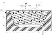
请参阅图1所示,本发明的光感测模块1包括一载体10、一光电二极管芯片20以及一光波长转换结构30。光感测模块1是用于接收一第一光束,并产生与第一光束的强度相对应的一电流。Please refer to FIG. 1 , the
载体10具有一承载面11与一内环侧表面12,承载面11与内环侧表面12相互连接,并形成一承载空间13。The
光电二极管芯片20位于承载空间13内,并设置于载体10的承载面11上。光电二极管芯片20位于载体10与光波长转换结构30之间,且被光波长转换结构30完整覆盖。The
光波长转换结构30位于承载空间13内,并设置于载体10的承载面11以及内环侧表面12上。光波长转换结构30可接收第一光束,并将第一光束转换成一第二光束,光电二极管芯片20接收第二光束后,会产生与第二光束的强度相对应的电流。由于电讯号与光讯号呈正比,故可通过量测光电二极管芯片20产生的电流大小,来推知第一光束的光强度,以达到感测第一光束的效果。The light
具体来说,本发明的光感测模块是紫外光感测模块,而光电二极管芯片20是可见光光电二极管。因此,光感测模块1接收的第一光束是紫外光,第一光束的频谱中具有一介于10纳米至400纳米之间的波峰。光波长转换结构30将第一光束(紫外光)转换成第二光束(可见光),以使光电二极管芯片20(可见光光电二极管)接收第二光束并产生电流,第二光束具有一介于400纳米至700纳米之间的频谱。Specifically, the light sensing module of the present invention is an ultraviolet light sensing module, and the
光波长转换结构的材料包括一萤光物质(fluorescent material)。荧光物质可将紫外光转换为可见光,因此,本发明可将可见光光电二极管应用于紫外光感测模块中。荧光物质是选自于由下列所构成的群组:含稀土元素的金属氧化物、含稀土元素的金属氮化物、含稀土元素的金属磷化物、含稀土元素的金属硅氧化物、含稀土元素的金属氮氧化物、含稀土元素的金属氧碳氮化物及其组合物。The material of the light wavelength conversion structure includes a fluorescent material. The fluorescent substance can convert ultraviolet light into visible light, therefore, the visible light photodiode can be applied to the ultraviolet light sensing module in the present invention. The fluorescent substance is selected from the group consisting of: rare earth element-containing metal oxide, rare earth element-containing metal nitride, rare earth element-containing metal phosphide, rare earth element-containing metal silicon oxide, rare earth element-containing metal oxide Metal oxynitrides, metal oxycarbonitrides containing rare earth elements and their compositions.
具体来说,荧光物质是选自于由下列所构成的群组:Ba2.0Eu0.6Mg3.2Al30.5Ox、(Ba,Sr)3.0Mg3.2Al30.5O51.9:Eu2+、BaMgAl10O17:Eu、Ba,Mg,Al10O17:Eu,Mn、CeMgAl11O19:Tb3+、Tb3Al5O12:Ce3+、La3Si6N11:Ce、(Ba,Sr)2Si5N8:Eu、(Sr,Ca)AlSiN3:Eu、(Sr,Ba)10(PO4)6Cl2:Eu、LaPO4:Ce,Tb、(Ba,Sr,Ca)2SiO4:Eu2+、Si6-zAlzOzN8-z:Eu及其组合物;其中,x为任意正数,z为小于6的任意正数。Specifically, the fluorescent substance is selected from the group consisting of Ba2.0 Eu0.6 Mg3.2 Al30.5 Ox , (Ba,Sr)3.0 Mg3.2 Al30.5 O51.9 :Eu2+ , BaMgAl10 O17 :Eu, Ba,Mg,Al10 O17 :Eu,Mn, CeMgAl11 O19 :Tb3+ , Tb3 Al5 O12 :Ce3+ , La3 Si6 N11 :Ce,(Ba,Sr)2 Si5 N8 :Eu, (Sr,Ca)AlSiN3 :Eu, (Sr,Ba)10 (PO4 )6 Cl2 :Eu, LaPO4 :Ce,Tb, (Ba,Sr,Ca)2 SiO4 : Eu2+ , Si6-z Alz Oz N8-z : Eu and combinations thereof; wherein, x is any positive number, and z is any positive number less than 6.
[对照组1][Control group 1]
为比较光感测模块的感测灵敏度,将一可见光发光二极管与一可见光光电二极管(即本发明的光电二极管芯片20)搭配使用,作为对照组1。经实验后,对照组1的可见光光电二极管产生3.789微安培(μA)的电流,并将此电流量订定为100%的目标值。In order to compare the sensing sensitivity of the light sensing module, a visible light emitting diode and a visible light photodiode (ie, the
[第一实施例][First Embodiment]
请参阅图1所示,第一实施例的光感测模块1包括前述载体10、光电二极管芯片20以及光波长转换结构30。光波长转换结构30的材料中包括一封装胶31以及一荧光物质32,荧光物质32均匀分散于封装胶31中。Referring to FIG. 1 , the
于本发明中,封装胶是透光性树脂。于一较佳实施例中,封装胶是具有一特定官能基的硅胶。例如苯基硅胶(phenyl silicone)、甲基硅胶(methylsilicone)或氟基硅胶(fluorosilicone)。在部分的实施例中,较佳是采用甲基硅胶或苯基硅胶,更佳是采用甲基硅胶,因为其等在紫外线C(UVC)的波长范围(100纳米至280纳米)下具有良好的穿透率。In the present invention, the encapsulant is a light-transmitting resin. In a preferred embodiment, the encapsulant is silica gel with a specific functional group. For example, phenyl silicone, methylsilicone or fluorosilicone. In some embodiments, methyl silica gel or phenyl silica gel is preferred, and methyl silica gel is more preferred because it has good performance in the ultraviolet C (UVC) wavelength range (100 nm to 280 nm). penetration rate.
[实验例1、2][Experimental example 1, 2]
实验例1、2的光感测模块对应于第一实施例(图1)中光感测模块的结构。请参表1所示,实验例1、2中分别使用不同的封装胶,以比较不同封装胶对光感测模块的感测灵敏度的影响。在实验例1、2中,先以紫外光照射光感测模块,再量测光电二极管芯片所产生的电流,并以对照组1的结果作为目标值的100%。The light sensing modules of Experimental Examples 1 and 2 correspond to the structures of the light sensing modules in the first embodiment ( FIG. 1 ). Please refer to Table 1. In Experimental Examples 1 and 2, different encapsulation adhesives were used to compare the effects of different encapsulation adhesives on the sensing sensitivity of the light sensing module. In experimental examples 1 and 2, the photo-sensing module was first irradiated with ultraviolet light, and then the current generated by the photodiode chip was measured, and the result of
在实验例1、2中,光波长转换结构的材料包括封装胶以及荧光物质,实验例1中的封装胶为苯基硅胶(例如道康宁公司所贩卖的OE-6650),实验例2中的封装胶为甲基硅胶(例如道康宁公司所贩卖的OE-6351)。实验例1、2中的荧光物质皆为含稀土元素的金属氧化物,其化学式为Tb3Al5O12:Ce3+(例如根本化学公司所贩卖的TAG-T3),且以光波长转换结构的总重为100重量百分比,荧光物质的含量为40重量百分比。In Experimental Examples 1 and 2, the materials of the optical wavelength conversion structure include encapsulant and fluorescent substances. The encapsulant in Experimental Example 1 is phenyl silica gel (such as OE-6650 sold by Dow Corning), and the encapsulant in Experimental Example 2 is The glue is methyl silica gel (eg, OE-6351 sold by Dow Corning). The fluorescent substances in the experimental examples 1 and 2 are all metal oxides containing rare earth elements, and their chemical formula is Tb3 Al5 O12 : Ce3+ (such as TAG-T3 sold by Basic Chemical Co., Ltd.), and the wavelength of light is converted. The total weight of the structure is 100% by weight, and the content of the fluorescent substance is 40% by weight.
表1Table 1

由表1的结果可得知,使用具有特定官能基的硅胶(甲基硅胶或苯基硅胶)作为封装胶,可提升光感测模块的感测灵敏度。并且,比较实施例1及实施例2,甲基硅胶(实验例2)相较于苯基硅胶(实验例1),更可提升光感测模块的感测灵敏度。From the results in Table 1, it can be known that using silica gel with specific functional groups (methyl silica gel or phenyl silica gel) as the encapsulant can improve the sensing sensitivity of the light sensing module. In addition, comparing Example 1 and Example 2, methyl silica gel (Experimental Example 2) can further improve the sensing sensitivity of the light sensing module compared to phenyl silica gel (Experimental Example 1).
[实验例3至11][Experimental Examples 3 to 11]
实验例3至11的光感测模块对应于第一实施例(图1)中光感测模块的结构。请参表2所示,实验例3至11中分别具有不同含量的荧光物质,以比较荧光物质的含量对光感测模块的感测灵敏度的影响。在实验例3至11中,先以紫外光照射光感测模块,再量测光电二极管芯片所产生的电流,并以对照组1的结果作为目标值的100%。The light sensing modules of Experimental Examples 3 to 11 correspond to the structures of the light sensing modules in the first embodiment ( FIG. 1 ). Please refer to Table 2. Experimental Examples 3 to 11 respectively have different contents of fluorescent substances to compare the influence of the contents of fluorescent substances on the sensing sensitivity of the light sensing module. In experimental examples 3 to 11, the photo-sensing module was first irradiated with ultraviolet light, and then the current generated by the photodiode chip was measured, and the result of
在实验例3至11中,光波长转换结构的材料包括封装胶以及荧光物质,封装胶是甲基硅胶,荧光物质为Tb3Al5O12:Ce3+,荧光物质的含量是基于光波长转换结构的总重为100重量百分比。In Experimental Examples 3 to 11, the material of the light wavelength conversion structure includes an encapsulant and a fluorescent substance, the encapsulant is methyl silica gel, the fluorescent substance is Tb3 Al5 O12 :Ce3+ , and the content of the fluorescent substance is based on the wavelength of the light The total weight of the transition structure is 100 weight percent.
表2Table 2

由表2的结果可得知,荧光物质的含量也会影响光感测模块对紫外光的灵敏度。于一些实施例中,以光波长转换结构的总重为100重量百分比,当荧光物质的含量为5重量百分比至80重量百分比时,可提升光感测模块的感测灵敏度。较佳的,以光波长转换结构的总重为100重量百分比,荧光物质的含量为7重量百分比至40重量百分比。更佳的,以光波长转换结构的总重为100重量百分比,荧光物质的含量为10重量百分比至40重量百分比。再更佳的,以光波长转换结构的总重为100重量百分比,荧光物质的含量为12重量百分比至30重量百分比。It can be known from the results in Table 2 that the content of the fluorescent substance also affects the sensitivity of the light sensing module to ultraviolet light. In some embodiments, when the total weight of the light wavelength conversion structure is 100 wt %, when the content of the fluorescent substance is 5 wt % to 80 wt %, the sensing sensitivity of the light sensing module can be improved. Preferably, the total weight of the light wavelength conversion structure is 100% by weight, and the content of the fluorescent substance is 7% by weight to 40% by weight. More preferably, the total weight of the light wavelength conversion structure is 100% by weight, and the content of the fluorescent substance is 10% by weight to 40% by weight. More preferably, the total weight of the light wavelength conversion structure is 100 weight percent, and the content of the fluorescent substance is 12 weight percent to 30 weight percent.
[第二实施例][Second Embodiment]
请参阅图2所示,第二实施例的光感测模块1与第一实施例的光感测模块1(图1)相似,其差异在于:光波长转换结构30的材料进一步包括一硅树脂粉末33(siliconepowder),硅树脂粉末33均匀分散于封装胶31中。Please refer to FIG. 2 , the
硅树脂粉末33的添加,可使光波长转换结构30的表面301形成有一微结构302(fine structure),以提供抗反射功效。请参阅图3所示,微观而言,微结构302在光波长转换结构30的表面上沿着一深度方向H形成,微结构302的折射率,会随着深度方向H而改变,当光线射入微结构发生连续反射时,可增加光线通过。The addition of the
[实验例12及比较例1][Experimental Example 12 and Comparative Example 1]
实验例12的光感测模块对应于第二实施例(图2)中光感测模块的结构。比较例1的光感测模块与实验例12的光感测模块相似,其差异在于:比较例1的光波长转换结构中并未添加硅树脂粉末,而是添加陶瓷二氧化硅粉末(ceramic silicon oxide powder)。The light sensing module of Experimental Example 12 corresponds to the structure of the light sensing module in the second embodiment ( FIG. 2 ). The light-sensing module of Comparative Example 1 is similar to the light-sensing module of Experimental Example 12. The difference is that the light wavelength conversion structure of Comparative Example 1 does not add silicone resin powder, but adds ceramic silicon dioxide powder. oxide powder).
请参表3所示,实验例12及比较例1中使用甲基硅胶作为封装胶。实验例12及比较例1中的荧光物质为Tb3Al5O12:Ce3+,基于光波长转换结构的总重为100重量百分比,荧光物质的含量是15重量百分比。基于光波长转换结构的总重为100重量百分比,实验例12中添加有60重量百分比的硅树脂粉末(信越化学公司生产的TS120),比较例1中添加有10重量百分比的陶瓷二氧化硅粉末。在实验例12及比较例1中,先以紫外光照射光感测模块,再量测光电二极管芯片所产生的电流,并以对照组1的结果作为目标值的100%。Please refer to Table 3. In Experimental Example 12 and Comparative Example 1, methyl silica gel was used as the encapsulant. The fluorescent substance in Experimental Example 12 and Comparative Example 1 was Tb3 Al5 O12 :Ce3+ , the total weight based on the light wavelength conversion structure was 100 wt %, and the content of the fluorescent substance was 15 wt %. Based on the total weight of the light wavelength conversion structure being 100% by weight, 60% by weight of silicone resin powder (TS120 produced by Shin-Etsu Chemical Co., Ltd.) was added in Experimental Example 12, and 10% by weight of ceramic silica powder was added in Comparative Example 1 . In Experimental Example 12 and Comparative Example 1, the light sensing module was first irradiated with ultraviolet light, and then the current generated by the photodiode chip was measured, and the result of the
表3table 3

由表3的结果可得知,于光波长转换结构中添加硅树脂粉末或陶瓷二氧化硅粉末,会影响光感测模块的感测灵敏度。From the results in Table 3, it can be known that adding silicone resin powder or ceramic silica powder to the light wavelength conversion structure will affect the sensing sensitivity of the light sensing module.
实验例7、12及比较例1的光转换模块,具有相似的结构及成分比例,其差异在于:实验例7未添加硅树脂粉末或陶瓷二氧化硅粉末,实验例12添加硅树脂粉末,比较例1添加陶瓷二氧化硅粉末。The light conversion modules of Experimental Examples 7, 12 and Comparative Example 1 have similar structures and component ratios. The difference is that in Experimental Example 7, no silicone resin powder or ceramic silica powder was added, and in Experimental Example 12, silicone resin powder was added. Example 1 Addition of ceramic silica powder.
由表2及表3的结果可得知,未添加硅树脂粉末或陶瓷二氧化硅粉末时,光电二极管芯片的目标值为70.9%(实验例7)。于光波长转换结构中添加硅树脂粉末,可提升光电二极管芯片的目标值至74.8%(实验例12)。于光波长转换结构中添加陶瓷二氧化硅粉末,反而会降低光电二极管芯片的目标值为65.3%(比较例1)。As can be seen from the results in Tables 2 and 3, when no silicone resin powder or ceramic silica powder was added, the target value of the photodiode chip was 70.9% (Experimental Example 7). Adding silicone resin powder to the light wavelength conversion structure can increase the target value of the photodiode chip to 74.8% (Experimental Example 12). Adding ceramic silica powder to the optical wavelength conversion structure instead lowered the target value of the photodiode chip by 65.3% (Comparative Example 1).
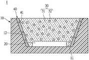
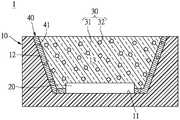
请参阅图4、图5所示,于一些实施例中,光感测模块1进一步包括一反射层40。反射层40设置于载体10的承载面11或内环侧表面12上,且反射层40位于载体10与光波长转换结构30之间。Referring to FIGS. 4 and 5 , in some embodiments, the
反射层40可反射光线,提升第一光束与第二光束被光电二极管芯片20接收的机率,进而提升光感测模块1的感测灵敏度。反射层40的材料包括一可见光反射填料41,可见光反射填料41均匀分散于反射层40中。可见光反射填料41可提升第二光束被光电二极管芯片20接收的机率,进而提升光感测模块1的感测灵敏度。The
具体来说,可见光反射填料41是选自于由下列所构成的群组:二氧化钛、氧化铝、氧化锌、二氧化硅、氮化硼及其组合物。以反射层40的总重为100重量百分比,可见光反射填料41的含量为20重量百分比至50重量百分比。Specifically, the visible light
[第三实施例][Third Embodiment]
请参阅图4所示,第三实施例的光感测模块1与第一实施例的光感测模块1(图1)相似,其差异在于:第三实施例的光感测模块1进一步包括一反射层40。反射层40设置于载体10的内环侧表面12上,且反射层40位于载体10与光波长转换结构30之间。Referring to FIG. 4 , the
[第四实施例][Fourth Embodiment]
请参阅图5所示,第四实施例的光感测模块1与第一实施例的光感测模块1(图1)相似,其差异在于:第四实施例的光感测模块1进一步包括一反射层40。反射层40设置于载体10的承载面11以及内环侧表面12上,且反射层40位于载体10与光波长转换结构30之间。Please refer to FIG. 5 , the
[实验例13、14][Experimental examples 13 and 14]
实验例13的光感测模块对应于第三实施例(图4)中光感测模块的结构,实验例14的光感测模块对应于第四实施例(图5)中光感测模块的结构。请参表4所示,实验例13、14中反射层设置的面积不同,以比较不同反射层设置面积对光感测模块的感测灵敏度的影响。在实验例13、14中,先以紫外光照射光感测模块,再量测光电二极管芯片所产生的电流,并以对照组1的结果作为目标值的100%。The optical sensing module of Experimental Example 13 corresponds to the structure of the optical sensing module in the third embodiment ( FIG. 4 ), and the optical sensing module of Experimental Example 14 corresponds to the optical sensing module of the fourth embodiment ( FIG. 5 ). structure. As shown in Table 4, the reflective layers in Experimental Examples 13 and 14 have different areas to compare the effects of different reflective layers on the sensing sensitivity of the light sensing module. In the experimental examples 13 and 14, the photo-sensing module was first irradiated with ultraviolet light, and then the current generated by the photodiode chip was measured, and the result of the
在实验例13、14中,光波长转换结构包括封装胶与荧光物质,封装胶是甲基硅胶,荧光物质为Tb3Al5O12:Ce3+,且以光波长转换结构的总重为100重量百分比,荧光物质的含量为15重量百分比。反射层包括可见光反射填料,可见光反射填料是二氧化钛。In Experimental Examples 13 and 14, the light wavelength conversion structure includes an encapsulant and a fluorescent substance, the encapsulant is methyl silica gel, the fluorescent substance is Tb3 Al5 O12 :Ce3+ , and the total weight of the light wavelength conversion structure is 100% by weight, the content of the fluorescent substance is 15% by weight. The reflective layer includes a visible light reflective filler, and the visible light reflective filler is titanium dioxide.
表4Table 4

由表4的结果可得知,载体上反射层设置的面积越大,可提升光感测模块的感测灵敏度。From the results in Table 4, it can be known that the larger the area of the reflective layer on the carrier is, the greater the sensing sensitivity of the light sensing module can be.
值得注意的是,实验例7、13及14的光转换模块,具有相似的结构及成分比例,其差异在于:实验例7未设置反射层,实验例13仅于载体的内环侧表面上设置反射层,实验例14同时于载体的承载面以及内环侧表面上设置反射层。It is worth noting that the light conversion modules of experimental examples 7, 13 and 14 have similar structures and component ratios, the difference is that: experimental example 7 does not have a reflective layer, and experimental example 13 is only provided on the inner ring side surface of the carrier Reflective layer, Experimental Example 14 At the same time, a reflective layer is provided on the bearing surface of the carrier and the side surface of the inner ring.
由表3及表4的结果可得知,实验例7中光电二极管芯片可达到的目标值为70.9%,实验例13中光电二极管芯片可达到的目标值为75.3%,实验例14中光电二极管芯片可达到的目标值为80.2%。据此,反射层的设置,可提升光感测模块的感测灵敏度可达到72%以上。并且,反射层可选择性设置于载体的承载面或是内环侧表面,于一较佳实施例中,当反射层同时设置于载体的承载面以及内环侧表面时,光感测模块的感测灵敏度可达到76%以上。From the results in Table 3 and Table 4, it can be known that the target value that can be achieved by the photodiode chip in Experimental Example 7 is 70.9%, the target value that can be achieved by the photodiode chip in Experimental Example 13 is 75.3%, and the photodiode in Experimental Example 14 The target value that can be achieved is 75.3%. The chip achievable target value is 80.2%. Accordingly, the setting of the reflective layer can improve the sensing sensitivity of the light sensing module by more than 72%. In addition, the reflective layer can be selectively disposed on the carrier surface or the inner ring side surface. In a preferred embodiment, when the reflective layer is simultaneously disposed on the carrier carrier surface and the inner ring side surface, the light sensing module The sensing sensitivity can reach more than 76%.
[第五实施例][Fifth Embodiment]
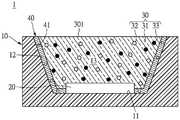
请参阅图6所示,第五实施例的光感测模块1与第四实施例的光感测模块1(图5)相似,其差异在于:除了封装胶31与荧光物质32之外,光波长转换结构30的材料进一步包括一硅树脂粉末33,硅树脂粉末33均匀分散于封装胶31中。因此,第五实施例的光波长转换结构30的表面301形成有一微结构302(如图3所示)。Referring to FIG. 6 , the
[实验例15至19][Experimental Examples 15 to 19]
实验例15至19的光感测模块对应于第五实施例(图6)中光感测模块的结构。请参表5所示,实验例15至19中的光波长转换结构具有不同含量的硅树脂粉末,以比较不同硅树脂粉末的添加量对光感测模块的感测灵敏度的影响。在实验例15至19中,先以紫外光照射光感测模块,再量测光电二极管芯片所产生的电流,并以对照组1的结果作为目标值的100%。The light sensing modules of Experimental Examples 15 to 19 correspond to the structures of the light sensing modules in the fifth embodiment ( FIG. 6 ). Please refer to Table 5. The optical wavelength conversion structures in Experimental Examples 15 to 19 have different contents of silicone resin powder, so as to compare the effects of different addition amounts of silicone resin powder on the sensing sensitivity of the optical sensing module. In Experimental Examples 15 to 19, the photo-sensing module was first irradiated with ultraviolet light, and then the current generated by the photodiode chip was measured, and the result of
在实验例15至19中,光波长转换结构的材料包括封装胶、荧光物质以及硅树脂粉末,封装胶是甲基硅胶,荧光物质为Tb3Al5O12:Ce3+。荧光物质的含量是基于光波长转换结构的总重为100重量百分比。硅树脂粉末的添加量是基于封装胶的总重为100重量份。In Experimental Examples 15 to 19, the materials of the light wavelength conversion structure include encapsulant, fluorescent substance and silicone resin powder, the encapsulant is methyl silica gel, and the fluorescent substance is Tb3 Al5 O12 :Ce3+ . The content of the fluorescent substance is 100 weight percent based on the total weight of the light wavelength conversion structure. The added amount of the silicone resin powder is 100 parts by weight based on the total weight of the encapsulant.
表5table 5

由表5的结果可得知,不同硅树脂粉末的添加量,会影响光感测模块的感测灵敏度。以封装胶的总重为100重量份,当硅树脂粉末的添加量为40重量份以上时,光电二极管芯片可达到75%以上的目标值。较佳的,当硅树脂粉末的添加量为50重量份至90重量份时,光电二极管芯片可达到80%以上的目标值。较佳的,当硅树脂粉末的添加量为60重量份至80重量份时,光电二极管芯片可达到82%以上的目标值。From the results in Table 5, it can be known that the addition amount of different silicone resin powders will affect the sensing sensitivity of the light sensing module. Taking the total weight of the encapsulant as 100 parts by weight, when the addition amount of the silicone resin powder is more than 40 parts by weight, the photodiode chip can reach the target value of more than 75%. Preferably, when the addition amount of the silicone resin powder is 50 to 90 parts by weight, the photodiode chip can reach the target value of more than 80%. Preferably, when the addition amount of the silicone resin powder is 60 to 80 parts by weight, the photodiode chip can reach the target value of more than 82%.
由表3及表4的结果可得知,实验例14中光电二极管芯片可达到的目标值为80.2%,实验例17中光电二极管芯片可达到的目标值为84.3%。据此,硅树脂粉末的添加,可提升光感测模块的感测灵敏度达到82%以上。From the results in Tables 3 and 4, it can be known that the target value that can be achieved by the photodiode chip in Experimental Example 14 is 80.2%, and the target value that can be achieved by the photodiode chip in Experimental Example 17 is 84.3%. Accordingly, the addition of the silicone resin powder can improve the sensing sensitivity of the light sensing module to more than 82%.
[对照组2][Control group 2]
不同的荧光物质,可产生不同的可见光频谱。因此,为比较不同荧光物质对光感测模块的感测灵敏度的影响,将一紫外光发光二极管搭配一紫外光光电二极管使用,作为对照组2。经实验后,对照组2的紫外光光电二极管产生14.59微安培(μA)的电流,并将此电流量订定为100%的目标值。Different fluorescent substances can produce different visible light spectrum. Therefore, in order to compare the effects of different fluorescent substances on the sensing sensitivity of the light sensing module, an ultraviolet light emitting diode and an ultraviolet light photodiode were used as the
[实验例20至32][Experimental Examples 20 to 32]
请参阅表6所示,实验例20至32是分别对不同的荧光物质的粉末进行激发测试。先以紫外光照射荧光物质粉末,再以可见光光电二极管接收经荧光物质粉末转换后的光线,并观察转换后光线频谱中的波峰波长值(简称为光转换波长)以及可见光光电二极管产生的电流,并以对照组2的结果作为目标值的100%。Please refer to Table 6. Experimental Examples 20 to 32 respectively conduct excitation tests on powders of different fluorescent substances. First, irradiate the fluorescent material powder with ultraviolet light, and then use the visible light photodiode to receive the light converted by the fluorescent material powder, and observe the peak wavelength value in the spectrum of the converted light (referred to as the light conversion wavelength) and the current generated by the visible light photodiode. And take the result of
表6Table 6

由表6的结果可得知,使用上述荧光物质皆可达到将紫外光(第一光束)转换为可见光(第二光束)的作用,不同的荧光物质,会使转换后的可见光(第二光束)具有不同的光线频谱。当荧光物质的光转换波长介于450纳米至650纳米,光电二极管芯片可达到45%至100%的目标值。较佳的,当荧光物质的光转换波长介于453纳米至647纳米,光电二极管芯片可达到45%至100%的目标值。更佳的,当荧光物质的光转换波长介于465纳米至625纳米,光电二极管芯片可达到70%至100%的目标值。From the results in Table 6, it can be known that the above fluorescent substances can be used to convert ultraviolet light (first beam) into visible light (second beam). Different fluorescent substances will cause the converted visible light (second beam). ) have different light spectrums. When the light conversion wavelength of the fluorescent substance is between 450 nm and 650 nm, the photodiode chip can reach the target value of 45% to 100%. Preferably, when the light conversion wavelength of the fluorescent substance is between 453 nm and 647 nm, the photodiode chip can reach the target value of 45% to 100%. More preferably, when the light conversion wavelength of the fluorescent substance is between 465 nm and 625 nm, the photodiode chip can reach the target value of 70% to 100%.
[实验例33至39][Experimental Examples 33 to 39]
实验例33至39的光感测模块对应于第五实施例(图6)中光感测模块的结构。请参阅表7所示,实验例33至39使用了另一种荧光物质(Ba,Sr)2Si5N8:Eu,取代实验例1至19中使用的荧光物质。并且,实验例33至39分别具有不同含量的荧光物质,以比较荧光物质的含量对光感测模块的感测灵敏度的影响。在实验例33至39中,先以紫外光照射光感测模块,再量测光电二极管芯片所产生的电流,并以对照组1的结果作为目标值的100%。The light sensing modules of Experimental Examples 33 to 39 correspond to the structures of the light sensing modules in the fifth embodiment ( FIG. 6 ). Referring to Table 7, Experimental Examples 33 to 39 used another fluorescent substance (Ba,Sr)2 Si5 N8 :Eu instead of the fluorescent substance used in Experimental Examples 1 to 19. In addition, experimental examples 33 to 39 respectively have different contents of fluorescent substances, so as to compare the influence of the contents of fluorescent substances on the sensing sensitivity of the light sensing module. In experimental examples 33 to 39, the photo-sensing module was first irradiated with ultraviolet light, and then the current generated by the photodiode chip was measured, and the result of
表7Table 7

由表7的结果可得知,选用不同的荧光物质,也会影响光感测模块对紫外光的灵敏度。于一些实施例中,以光波长转换结构的总重为100重量百分比,荧光物质的含量为5重量百分比至80重量百分比。较佳的,以光波长转换结构的总重为100重量百分比,荧光物质的含量为7重量百分比至40重量百分比。更佳的,以光波长转换结构的总重为100重量百分比,荧光物质的含量为10重量百分比至40重量百分比。再更佳的,以光波长转换结构的总重为100重量百分比,荧光物质的含量为12重量百分比至30重量百分比。From the results in Table 7, it can be known that the selection of different fluorescent substances will also affect the sensitivity of the light sensing module to ultraviolet light. In some embodiments, the total weight of the light wavelength conversion structure is 100% by weight, and the content of the fluorescent substance is 5% by weight to 80% by weight. Preferably, the total weight of the light wavelength conversion structure is 100% by weight, and the content of the fluorescent substance is 7% by weight to 40% by weight. More preferably, the total weight of the light wavelength conversion structure is 100% by weight, and the content of the fluorescent substance is 10% by weight to 40% by weight. More preferably, the total weight of the light wavelength conversion structure is 100 weight percent, and the content of the fluorescent substance is 12 weight percent to 30 weight percent.
由表5及表7的结果可得知,实验例18中光电二极管芯片可达到的目标值为85.1%,实验例37光电二极管芯片可达到的目标值为89.3%。据此,当荧光物质的光转换波长介于500纳米至620纳米,光电二极管芯片可达到75%至100%的目标值。较佳的,当荧光物质的光转换波长介于550纳米至620纳米,光电二极管芯片可达到80%至100%的目标值。更佳的,当荧光物质的光转换波长介于570纳米至610纳米,光电二极管芯片可达到88%至100%的目标值。From the results in Table 5 and Table 7, it can be known that the target value that can be achieved by the photodiode chip in Experimental Example 18 is 85.1%, and the target value that can be achieved by the photodiode chip in Experimental Example 37 is 89.3%. Accordingly, when the light conversion wavelength of the fluorescent substance is between 500 nm and 620 nm, the photodiode chip can reach the target value of 75% to 100%. Preferably, when the light conversion wavelength of the fluorescent substance is between 550 nm and 620 nm, the photodiode chip can reach the target value of 80% to 100%. More preferably, when the light conversion wavelength of the fluorescent substance is between 570 nm and 610 nm, the photodiode chip can reach the target value of 88% to 100%.
请参阅图7所示,于一些实施例中,除了可见光反射填料41之外,反射层40的材料可进一步包括一紫外光反射填料42。紫外光反射填料42的添加,可增加第一光束被荧光物质32转换为第二光束的机率,进而提升光感测模块1的感测灵敏度。Referring to FIG. 7 , in some embodiments, in addition to the visible light
[第六实施例][Sixth Embodiment]
请参阅图7所示,第六实施例的光感测模块1与第五实施例的光感测模块1(图6)相似,其差异在于:反射层40的材料进一步包括一紫外光反射填料42,紫外光反射填料42均匀分散于反射层40中。Please refer to FIG. 7 , the
具体来说,紫外光反射填料42是选自于由下列所构成的群组:聚四氟乙烯、二氧化锆、氮化铝、及其组合物。以反射层40的总重为100重量百分比,紫外光反射填料42的含量为10重量百分比至80重量百分比。Specifically, the UV
[实验例40][Experimental Example 40]
实验例40的光感测模块对应于第六实施例(图7)中光感测模块的结构。请参表8所示,实验例40的反射层中进一步包括紫外光反射填料,且紫外光反射填料是聚四氟乙烯(L206),以反射层的总重为100重量百分比,紫外光反射填料的含量为80重量百分比。在实验例40中,先以紫外光照射光感测模块,再量测光电二极管芯片所产生的电流,并以对照组1的结果作为目标值的100%。The light sensing module of Experimental Example 40 corresponds to the structure of the light sensing module in the sixth embodiment ( FIG. 7 ). Please refer to Table 8, the reflective layer of Experimental Example 40 further includes a UV reflective filler, and the UV reflective filler is polytetrafluoroethylene (L206), and the total weight of the reflective layer is 100% by weight, and the UV reflective filler The content is 80 weight percent. In Experimental Example 40, the light sensing module was first irradiated with ultraviolet light, and then the current generated by the photodiode chip was measured, and the result of
在实验例40中,光波长转换结构的材料包括封装胶、荧光物质以及硅树脂粉末,封装胶是甲基硅胶,荧光物质为Tb3Al5O12:Ce3+。以光波长转换结构的总重为100重量百分比,荧光物质的含量为15重量百分比,硅树脂粉末的含量为80重量百分比。反射层的材料中包括可见光反射填料(二氧化钛)与紫外光反射填料(聚四氟乙烯),以光波长转换结构的总重为100重量百分比,可见光反射填料的含量为重量百分比,紫外光反射填料的含量为80重量百分比。In Experimental Example 40, the material of the light wavelength conversion structure includes encapsulant, fluorescent substance and silicone resin powder, the encapsulant is methyl silica gel, and the fluorescent substance is Tb3 Al5 O12 :Ce3+ . The total weight of the light wavelength conversion structure is 100% by weight, the content of the fluorescent substance is 15% by weight, and the content of the silicone resin powder is 80% by weight. The material of the reflective layer includes visible light reflective filler (titanium dioxide) and ultraviolet light reflective filler (polytetrafluoroethylene), the total weight of the light wavelength conversion structure is 100 weight percent, the content of the visible light reflective filler is weight percent, and the ultraviolet light reflective filler is The content is 80 weight percent.
表8Table 8

由表8的结果可得知,紫外光反射填料的添加,可提升光感测模块的感测灵敏度。于一些实施例中,以光波长转换结构的总重为100重量百分比,紫外光反射填料的含量大于或等于40重量百分比。较佳的,以光波长转换结构的总重为100重量百分比,紫外光反射填料的含量为50重量百分比至90重量百分比。更佳的,以光波长转换结构的总重为100重量百分比,紫外光反射填料的含量为60重量百分比至85重量百分比。From the results in Table 8, it can be known that the addition of the ultraviolet light reflective filler can improve the sensing sensitivity of the light sensing module. In some embodiments, with the total weight of the light wavelength conversion structure being 100 weight percent, the content of the ultraviolet light reflective filler is greater than or equal to 40 weight percent. Preferably, the total weight of the light wavelength conversion structure is 100% by weight, and the content of the ultraviolet light reflective filler is 50% by weight to 90% by weight. More preferably, the total weight of the light wavelength conversion structure is 100 weight percent, and the content of the ultraviolet light reflective filler is 60 weight percent to 85 weight percent.
值得注意的是,实验例18及实验例40的光转换模块,具有相似的结构及成分比例,其差异在于:实验例40中的反射层,相较于实验例18额外添加了聚四氟乙烯(紫外光反射填料)。It is worth noting that the light conversion modules of Experimental Example 18 and Experimental Example 40 have similar structures and component ratios. The difference is that compared to Experimental Example 18, the reflective layer in Experimental Example 40 is additionally added with polytetrafluoroethylene. (UV reflective filler).
由表5及表8的结果可得知,实验例18中光电二极管芯片可达到的目标值为85.1%,实验例40光电二极管芯片可达到的目标值为92.4%。据此,于反射层中额外添加了紫外光反射填料,可进一步使光电二极管芯片可达到90%至100%的目标值。From the results in Table 5 and Table 8, it can be known that the target value that can be achieved by the photodiode chip in Experimental Example 18 is 85.1%, and the target value that can be achieved by the photodiode chip in Experimental Example 40 is 92.4%. Accordingly, the ultraviolet light reflective filler is additionally added to the reflective layer, which can further enable the photodiode chip to reach the target value of 90% to 100%.
请参阅图8所示,本发明另提供一种电子装置3,电子装置3包括一光发射模块2以及前述的光感测模块1。光发射模块2可产生一第一光束。光感测模块1可接收第一光束,并产生与第一光束的强度相对应的一电流。Referring to FIG. 8 , the present invention further provides an electronic device 3 . The electronic device 3 includes a
具体来说,光感测模块1包括前述的载体10、光电二极管芯片20与光波长转换结构30,光感测模块1的详细结构如前所述,于此不再赘述。具体来说,光发射模块2包括一发光二极管芯片,发光二极管芯片可产生第一光束。Specifically, the
于一些实施例中,光发射模块2可产生紫外光(第一光束),即第一光束具有一介于10纳米至400纳米之间的波峰。光感测模块1中的光波长转换结构30可将紫外光(第一光束)转换为可见光(第二光束),即第一光束具有一介于400纳米至700纳米之间的波峰。接着,光电二极管芯片20于接收第二光束后,会产生与第二光束的强度相对应的一电流。In some embodiments, the
[实施例的有益效果][Advantageous effects of the embodiment]
本发明的其中一有益效果在于,本发明所提供的光感测模块,其能通过“所述光波长转换结构30接收所述第一光束转换成一第二光束”以及“所述光电二极管芯片20接收所述第二光束并产生所述电流”的技术方案,以达到降低光感测模块1的成本的效果。One of the beneficial effects of the present invention is that the light sensing module provided by the present invention can receive the first light beam and convert it into a second light beam through "the light
更进一步来说,本发明所提供的光感测模块,其能通过“所述光波长转换结构的材料包括一封装胶,所述封装胶是具有甲基的硅胶或具有苯基的硅胶”的技术方案,以达到提升光感测模块1的灵敏度的功效。More specifically, the light sensing module provided by the present invention can pass through "the material of the light wavelength conversion structure includes an encapsulant, and the encapsulant is silica gel with methyl groups or silica gel with phenyl groups". The technical solution is to achieve the effect of improving the sensitivity of the
更进一步来说,本发明所提供的光感测模块,其能通过“所述第二光束具有一介于453纳米至647纳米之间频谱”以及“所述第二光束具有一介于465纳米至625纳米之间频谱”的技术方案,以达到提升光感测模块1的灵敏度的功效。Furthermore, the light sensing module provided by the present invention can pass "the second light beam has a spectrum between 453 nm and 647 nm" and "the second light beam has a spectrum between 465 nm and 625 nm". The technical solution of "spectrum between nanometers" can achieve the effect of improving the sensitivity of the
更进一步来说,本发明所提供的光感测模块,其能通过“所述光波长转换结构30的材料包括一硅树脂粉末33”的技术方案,以达到提升光感测模块1的灵敏度的功效。Furthermore, in the light sensing module provided by the present invention, the technical solution of "the material of the light
更进一步来说,本发明所提供的光感测模块,其能通过“所述反射层40的材料包括一可见光反射填料41”以及“所述反射层40的材料包括一紫外光反射填料42”的技术方案,以达到提升光感测模块1的灵敏度的功效。Furthermore, the light sensing module provided by the present invention can pass through "the material of the
以上所公开的内容仅为本发明的优选可行实施例,并非因此局限本发明的权利要求书的保护范围,所以凡是运用本发明说明书及附图内容所做的等效技术变化,均包含于本发明的权利要求书的保护范围内。The content disclosed above is only a preferred feasible embodiment of the present invention, and is not intended to limit the protection scope of the claims of the present invention. Therefore, any equivalent technical changes made by using the contents of the description and the accompanying drawings of the present invention are included in the present invention. within the protection scope of the claims of the invention.
Claims (19)
Priority Applications (2)
| Application Number | Priority Date | Filing Date | Title |
|---|---|---|---|
| CN202011255911.0ACN114551627B (en) | 2020-11-11 | 2020-11-11 | Light sensing module |
| US17/517,750US20220149214A1 (en) | 2020-11-11 | 2021-11-03 | Light sensor module |
Applications Claiming Priority (1)
| Application Number | Priority Date | Filing Date | Title |
|---|---|---|---|
| CN202011255911.0ACN114551627B (en) | 2020-11-11 | 2020-11-11 | Light sensing module |
Publications (2)
| Publication Number | Publication Date |
|---|---|
| CN114551627Atrue CN114551627A (en) | 2022-05-27 |
| CN114551627B CN114551627B (en) | 2024-10-29 |
Family
ID=81453857
Family Applications (1)
| Application Number | Title | Priority Date | Filing Date |
|---|---|---|---|
| CN202011255911.0AActiveCN114551627B (en) | 2020-11-11 | 2020-11-11 | Light sensing module |
Country Status (2)
| Country | Link |
|---|---|
| US (1) | US20220149214A1 (en) |
| CN (1) | CN114551627B (en) |
Families Citing this family (1)
| Publication number | Priority date | Publication date | Assignee | Title |
|---|---|---|---|---|
| KR102519070B1 (en)* | 2022-07-11 | 2023-04-07 | 주식회사 루트센서 | Optical sensor and electronic device including thereof |
Citations (10)
| Publication number | Priority date | Publication date | Assignee | Title |
|---|---|---|---|---|
| US20030080341A1 (en)* | 2001-01-24 | 2003-05-01 | Kensho Sakano | Light emitting diode, optical semiconductor element and epoxy resin composition suitable for optical semiconductor element and production methods therefor |
| JP2005216384A (en)* | 2004-01-29 | 2005-08-11 | Sharp Corp | Optical pickup device |
| JP2005247661A (en)* | 2004-03-05 | 2005-09-15 | Matsushita Electric Works Ltd | Silica aerogel, method for manufacturing silica aerogel, and apparatus for detecting elementary particle |
| CN101022139A (en)* | 2006-02-15 | 2007-08-22 | 财团法人工业技术研究院 | Light sensing element and its manufacturing method |
| CN102017167A (en)* | 2008-04-29 | 2011-04-13 | 皇家飞利浦电子股份有限公司 | Photo-detector with wavelength converter |
| US20110162711A1 (en)* | 2008-06-06 | 2011-07-07 | Sumitomo Bakelite Co., Ltd. | Wavelength-converting composition and photovoltaic device comprising layer composed of wavelength-converting composition |
| CN104332524A (en)* | 2014-08-26 | 2015-02-04 | 日月光半导体制造股份有限公司 | Electronic device, optical module and manufacturing method thereof |
| US20150102374A1 (en)* | 2012-05-21 | 2015-04-16 | Osram Opto Semiconductors Gmbh | Optoelectronic component and method for producing it |
| CN205911310U (en)* | 2016-07-18 | 2017-01-25 | 研晶光电股份有限公司 | Light source module |
| WO2018047757A1 (en)* | 2016-09-07 | 2018-03-15 | 住友化学株式会社 | Wavelength conversion material-containing silicone resin composition, and wavelength conversion material-containing sheet |
Family Cites Families (8)
| Publication number | Priority date | Publication date | Assignee | Title |
|---|---|---|---|---|
| US4096387A (en)* | 1976-12-09 | 1978-06-20 | Rca Corporation | Ultraviolet radiation detector |
| JP4211359B2 (en)* | 2002-03-06 | 2009-01-21 | 日亜化学工業株式会社 | Manufacturing method of semiconductor device |
| US20110120554A1 (en)* | 2008-03-27 | 2011-05-26 | Rensselaer Polytechnic Institute | Ultra-low reflectance broadband omni-directional anti-reflection coating |
| DE102011009819A1 (en)* | 2011-01-31 | 2012-02-16 | Mitsubishi Polyester Film Gmbh | A biaxially stretched polyester film having a high cyclohexanedimethanol content and a secondary diol content, and a primary and secondary dicarboxylic acid portion, and a process for their preparation and their use |
| KR102338448B1 (en)* | 2014-07-23 | 2021-12-10 | 린텍 가부시키가이샤 | Curable composition, method for manufacturing curable composition, cured product, method for using curable composition, and optical device |
| US9716190B2 (en)* | 2015-03-23 | 2017-07-25 | Sii Semiconductor Corporation | Optical sensor device and method of manufacturing optical sensor device |
| KR102725510B1 (en)* | 2018-12-17 | 2024-11-04 | 킹 압둘라 유니버시티 오브 사이언스 앤드 테크놀로지 | Ultraviolet detection with high-speed wavelength conversion layer |
| WO2020170841A1 (en)* | 2019-02-21 | 2020-08-27 | ソニーセミコンダクタソリューションズ株式会社 | Avalanche-photodiode sensor and distance measurement device |
- 2020
- 2020-11-11CNCN202011255911.0Apatent/CN114551627B/enactiveActive
- 2021
- 2021-11-03USUS17/517,750patent/US20220149214A1/ennot_activeAbandoned
Patent Citations (10)
| Publication number | Priority date | Publication date | Assignee | Title |
|---|---|---|---|---|
| US20030080341A1 (en)* | 2001-01-24 | 2003-05-01 | Kensho Sakano | Light emitting diode, optical semiconductor element and epoxy resin composition suitable for optical semiconductor element and production methods therefor |
| JP2005216384A (en)* | 2004-01-29 | 2005-08-11 | Sharp Corp | Optical pickup device |
| JP2005247661A (en)* | 2004-03-05 | 2005-09-15 | Matsushita Electric Works Ltd | Silica aerogel, method for manufacturing silica aerogel, and apparatus for detecting elementary particle |
| CN101022139A (en)* | 2006-02-15 | 2007-08-22 | 财团法人工业技术研究院 | Light sensing element and its manufacturing method |
| CN102017167A (en)* | 2008-04-29 | 2011-04-13 | 皇家飞利浦电子股份有限公司 | Photo-detector with wavelength converter |
| US20110162711A1 (en)* | 2008-06-06 | 2011-07-07 | Sumitomo Bakelite Co., Ltd. | Wavelength-converting composition and photovoltaic device comprising layer composed of wavelength-converting composition |
| US20150102374A1 (en)* | 2012-05-21 | 2015-04-16 | Osram Opto Semiconductors Gmbh | Optoelectronic component and method for producing it |
| CN104332524A (en)* | 2014-08-26 | 2015-02-04 | 日月光半导体制造股份有限公司 | Electronic device, optical module and manufacturing method thereof |
| CN205911310U (en)* | 2016-07-18 | 2017-01-25 | 研晶光电股份有限公司 | Light source module |
| WO2018047757A1 (en)* | 2016-09-07 | 2018-03-15 | 住友化学株式会社 | Wavelength conversion material-containing silicone resin composition, and wavelength conversion material-containing sheet |
Also Published As
| Publication number | Publication date |
|---|---|
| CN114551627B (en) | 2024-10-29 |
| US20220149214A1 (en) | 2022-05-12 |
Similar Documents
| Publication | Publication Date | Title |
|---|---|---|
| TW578313B (en) | Opto-electronic component | |
| US8138671B2 (en) | Color-stable phosphor converted LED | |
| CN105358615B (en) | Additives for Silicone Encapsulation Materials | |
| JP4922189B2 (en) | Optical element, method for manufacturing element that emits radiation, optical element, and element that emits radiation | |
| JP5743548B2 (en) | Lighting device | |
| JP5355544B2 (en) | Optoelectronic device emitting electromagnetic radiation and method of manufacturing an optoelectronic device | |
| US9773953B2 (en) | Organic phosphor-functionalized nanoparticles and compositions comprising the same | |
| JP2016537810A (en) | LED encapsulant | |
| TW201927929A (en) | LED filament lamps with white filament appearance | |
| US9741910B1 (en) | Optoelectronic component | |
| CN103262267A (en) | Optoelectronic semiconductor component | |
| US10032962B2 (en) | LED package structure | |
| CN102652369B (en) | Optoelectronic semiconductor components | |
| TW201914060A (en) | Quantum dot-based color-converted light emitting device and method for manufacturing the same | |
| CN108666407A (en) | Light emitting diode packaging structure with surface light source and manufacturing method thereof | |
| CN108367916A (en) | Conversion element has its opto-electronic device, and the method for manufacture conversion element | |
| CN114551627B (en) | Light sensing module | |
| CN103187515A (en) | Light conversion structure and packaging structure of light emitting diode applying same | |
| TW200836379A (en) | Light emitting semiconductor device | |
| CN103820118B (en) | Phosphor composition and the light emitting device packaging piece with this phosphor composition | |
| CN108538987A (en) | Optical semiconductor device and package for optical semiconductor device | |
| CN219759608U (en) | Packaging structure | |
| RU2524234C2 (en) | Luminescent coating for improving efficiency of converting energy of incident light and method of producing said coating | |
| US8569610B2 (en) | Light-emitting polymer | |
| JP2011222852A (en) | Optical semiconductor device |
Legal Events
| Date | Code | Title | Description |
|---|---|---|---|
| PB01 | Publication | ||
| PB01 | Publication | ||
| SE01 | Entry into force of request for substantive examination | ||
| SE01 | Entry into force of request for substantive examination | ||
| GR01 | Patent grant | ||
| GR01 | Patent grant |