CN114546101A - Tactile sense reproduction device, display panel, and display device - Google Patents
Tactile sense reproduction device, display panel, and display deviceDownload PDFInfo
- Publication number
- CN114546101A CN114546101ACN202011333604.XACN202011333604ACN114546101ACN 114546101 ACN114546101 ACN 114546101ACN 202011333604 ACN202011333604 ACN 202011333604ACN 114546101 ACN114546101 ACN 114546101A
- Authority
- CN
- China
- Prior art keywords
- electrode
- temperature control
- end electrode
- semiconductor
- semiconductor temperature
- Prior art date
- Legal status (The legal status is an assumption and is not a legal conclusion. Google has not performed a legal analysis and makes no representation as to the accuracy of the status listed.)
- Granted
Links
Images


Classifications
- H—ELECTRICITY
- H01—ELECTRIC ELEMENTS
- H01L—SEMICONDUCTOR DEVICES NOT COVERED BY CLASS H10
- H01L23/00—Details of semiconductor or other solid state devices
- H01L23/34—Arrangements for cooling, heating, ventilating or temperature compensation ; Temperature sensing arrangements
- H01L23/38—Cooling arrangements using the Peltier effect
- G—PHYSICS
- G06—COMPUTING OR CALCULATING; COUNTING
- G06F—ELECTRIC DIGITAL DATA PROCESSING
- G06F3/00—Input arrangements for transferring data to be processed into a form capable of being handled by the computer; Output arrangements for transferring data from processing unit to output unit, e.g. interface arrangements
- G06F3/01—Input arrangements or combined input and output arrangements for interaction between user and computer
- G06F3/016—Input arrangements with force or tactile feedback as computer generated output to the user
- G—PHYSICS
- G06—COMPUTING OR CALCULATING; COUNTING
- G06F—ELECTRIC DIGITAL DATA PROCESSING
- G06F3/00—Input arrangements for transferring data to be processed into a form capable of being handled by the computer; Output arrangements for transferring data from processing unit to output unit, e.g. interface arrangements
- G06F3/01—Input arrangements or combined input and output arrangements for interaction between user and computer
- G06F3/03—Arrangements for converting the position or the displacement of a member into a coded form
- G06F3/041—Digitisers, e.g. for touch screens or touch pads, characterised by the transducing means
- G06F3/0412—Digitisers structurally integrated in a display
- H—ELECTRICITY
- H10—SEMICONDUCTOR DEVICES; ELECTRIC SOLID-STATE DEVICES NOT OTHERWISE PROVIDED FOR
- H10K—ORGANIC ELECTRIC SOLID-STATE DEVICES
- H10K59/00—Integrated devices, or assemblies of multiple devices, comprising at least one organic light-emitting element covered by group H10K50/00
- H10K59/40—OLEDs integrated with touch screens
- H—ELECTRICITY
- H10—SEMICONDUCTOR DEVICES; ELECTRIC SOLID-STATE DEVICES NOT OTHERWISE PROVIDED FOR
- H10N—ELECTRIC SOLID-STATE DEVICES NOT OTHERWISE PROVIDED FOR
- H10N10/00—Thermoelectric devices comprising a junction of dissimilar materials, i.e. devices exhibiting Seebeck or Peltier effects
- H10N10/10—Thermoelectric devices comprising a junction of dissimilar materials, i.e. devices exhibiting Seebeck or Peltier effects operating with only the Peltier or Seebeck effects
- H10N10/17—Thermoelectric devices comprising a junction of dissimilar materials, i.e. devices exhibiting Seebeck or Peltier effects operating with only the Peltier or Seebeck effects characterised by the structure or configuration of the cell or thermocouple forming the device
- H—ELECTRICITY
- H10—SEMICONDUCTOR DEVICES; ELECTRIC SOLID-STATE DEVICES NOT OTHERWISE PROVIDED FOR
- H10N—ELECTRIC SOLID-STATE DEVICES NOT OTHERWISE PROVIDED FOR
- H10N10/00—Thermoelectric devices comprising a junction of dissimilar materials, i.e. devices exhibiting Seebeck or Peltier effects
- H10N10/80—Constructional details
- H10N10/85—Thermoelectric active materials
- H10N10/851—Thermoelectric active materials comprising inorganic compositions
- H10N10/855—Thermoelectric active materials comprising inorganic compositions comprising compounds containing boron, carbon, oxygen or nitrogen
- H—ELECTRICITY
- H10—SEMICONDUCTOR DEVICES; ELECTRIC SOLID-STATE DEVICES NOT OTHERWISE PROVIDED FOR
- H10N—ELECTRIC SOLID-STATE DEVICES NOT OTHERWISE PROVIDED FOR
- H10N10/00—Thermoelectric devices comprising a junction of dissimilar materials, i.e. devices exhibiting Seebeck or Peltier effects
- H10N10/80—Constructional details
- H10N10/85—Thermoelectric active materials
- H10N10/851—Thermoelectric active materials comprising inorganic compositions
- H10N10/8556—Thermoelectric active materials comprising inorganic compositions comprising compounds containing germanium or silicon
Landscapes
- Engineering & Computer Science (AREA)
- General Engineering & Computer Science (AREA)
- Theoretical Computer Science (AREA)
- Physics & Mathematics (AREA)
- General Physics & Mathematics (AREA)
- Chemical & Material Sciences (AREA)
- Human Computer Interaction (AREA)
- Inorganic Chemistry (AREA)
- Condensed Matter Physics & Semiconductors (AREA)
- Computer Hardware Design (AREA)
- Microelectronics & Electronic Packaging (AREA)
- Power Engineering (AREA)
- User Interface Of Digital Computer (AREA)
Abstract
Description
Translated fromChinese技术领域technical field
本发明涉及触觉再现技术领域,具体而言,涉及一种触觉再现装置、显示面板和显示装置。The present invention relates to the technical field of haptic reproduction, and in particular, to a haptic reproduction device, a display panel and a display device.
背景技术Background technique
作为新兴的人机交互技术,表面触觉再现技术能够通过裸指触摸屏幕来感知物体特性,在多媒体终端实现高效自然的交互,具有巨大的研究价值。表面触觉再现技术是在一载体平面上设置振动源(如压电陶瓷芯片),使载体因共振而发生机械变形,形成一定的摩擦力,从而实现不同触觉/触感的模拟。As an emerging human-computer interaction technology, surface tactile reproduction technology can sense the characteristics of objects by touching the screen with bare fingers, and realize efficient and natural interaction in multimedia terminals, which has great research value. The surface tactile reproduction technology is to set a vibration source (such as a piezoelectric ceramic chip) on a carrier plane, so that the carrier is mechanically deformed due to resonance, forming a certain friction force, thereby realizing the simulation of different tactile/tactile sensations.
人体接触物体表面时,除了能够感知到上述力学信号,还能感知温觉信号,由此才能更准确、更丰富的感知物体表面特性。然而,由于载体材质的比热的固定不变的,只能实现单一种质料的温觉,感受较为单一。而且载体在发生共振时,会因本身振动时阻尼产生发热现象,发热现象会使共振效率与共振峰产生偏移,影响触觉模拟的准确性。同时,由于形变量不同,载体表面热量也分布不均匀。When the human body touches the surface of an object, in addition to the above-mentioned mechanical signals, it can also perceive the temperature sensory signal, so that the surface characteristics of the object can be perceived more accurately and abundantly. However, since the specific heat of the carrier material is fixed, only the temperature sensation of a single material can be realized, and the feeling is relatively simple. Moreover, when the carrier resonates, it will generate heat due to the damping of its own vibration, and the heat phenomenon will cause the resonance efficiency to shift from the formant peak, which will affect the accuracy of the tactile simulation. At the same time, due to the different deformations, the heat distribution on the surface of the carrier is also uneven.
需要说明的是,在上述背景技术部分发明的信息仅用于加强对本发明的背景的理解,因此可以包括不构成对本领域普通技术人员已知的现有技术的信息。It should be noted that the information disclosed in the above Background section is only for enhancing understanding of the background of the invention, and therefore may include information that does not form the prior art known to a person of ordinary skill in the art.
发明内容SUMMARY OF THE INVENTION
本发明的目的在于提供一种触觉再现装置、显示面板和显示装置,解决现有技术存在的一种或多种问题。The purpose of the present invention is to provide a haptic reproduction device, a display panel and a display device to solve one or more problems existing in the prior art.
根据本发明的第一个方面,提供一种触觉再现装置,包括:According to a first aspect of the present invention, there is provided a haptic reproduction device, comprising:
基板,包括在第一方向上依次交替排列的多个形变区和多个节点区,所述基板能够发生振动,使所述形变区发生形变,所述节点区不发生形变;a substrate, comprising a plurality of deformation regions and a plurality of node regions alternately arranged in sequence in the first direction, the substrate can vibrate, so that the deformation regions are deformed, and the node regions are not deformed;
半导体控温组件,包括多个设于所述基板的一面且沿所述第一方向排列的半导体控温单元,所述半导体控温单元包括热端电极、P端电极、N端电极、P型半导体和N型半导体,各所述热端电极设于各所述形变区,各所述P端电极、N端电极设于各所述节点区,所述P型半导体连接所述P端电极和热端电极,所述N型半导体连接所述N端电极和热端电极。A semiconductor temperature control assembly, comprising a plurality of semiconductor temperature control units arranged on one side of the substrate and arranged along the first direction, the semiconductor temperature control units including a hot end electrode, a P end electrode, an N end electrode, a P type A semiconductor and an N-type semiconductor, each of the hot-end electrodes is arranged in each of the deformation regions, each of the P-end electrodes and N-end electrodes are arranged in each of the node regions, and the P-type semiconductor is connected to the P-end electrode and the N-type semiconductor. A hot terminal electrode, the N-type semiconductor is connected to the N terminal electrode and the hot terminal electrode.
在本发明的一种示例性实施例中,各所述半导体控温单元中,所述P端电极包括第一P端电极和第二P端电极,所述N端电极包括第一N端电极和第二N端电极,所述P型半导体包括第一P型半导体和第二P型半导体,所述N型半导体包括第一N型半导体和第二N型半导体;In an exemplary embodiment of the present invention, in each of the semiconductor temperature control units, the P-terminal electrode includes a first P-terminal electrode and a second P-terminal electrode, and the N-terminal electrode includes a first N-terminal electrode and a second N-terminal electrode, the P-type semiconductor includes a first P-type semiconductor and a second P-type semiconductor, and the N-type semiconductor includes a first N-type semiconductor and a second N-type semiconductor;
其中,所述热端电极设于一个所述形变区,所述第一P端电极和第一N端电极设于所述热端电极一侧的所述节点区,所述第一P型半导体连接所述第一P端电极和所述热端电极,所述第一N型半导体连接所述第一N端电极和所述热端电极;所述第二P端电极和第二N端电极设于所述热端电极另一侧的节点区,所述第二P型半导体连接所述第二P端电极和所述热端电极,所述第二N型半导体连接所述第二N端电极和所述热端电极;Wherein, the hot end electrode is arranged in one of the deformation regions, the first P end electrode and the first N end electrode are arranged in the node region on one side of the hot end electrode, and the first P-type semiconductor connecting the first P-terminal electrode and the hot-terminal electrode, the first N-type semiconductor connecting the first N-terminal electrode and the hot-terminal electrode; the second P-terminal electrode and the second N-terminal electrode A node region located on the other side of the hot terminal electrode, the second P-type semiconductor is connected to the second P terminal electrode and the hot terminal electrode, and the second N-type semiconductor is connected to the second N terminal an electrode and the hot end electrode;
其中,在所述第一方向上相邻的两个所述半导体控温单元中,一个所述半导体控温单元中的第一P端电极、第一N端电极和另一个所述半导体控温单元中的第二P端电极、第二N端电极设于同一个所述节点区。Wherein, in the two adjacent semiconductor temperature control units in the first direction, the first P terminal electrode and the first N terminal electrode in one of the semiconductor temperature control units and the other semiconductor temperature control unit The second P-terminal electrode and the second N-terminal electrode in the unit are arranged in the same node region.
在本发明的一种示例性实施例中,位于同一个所述节点区的第一P端电极和第二P端电极连接为一体或各自独立,位于同一个所述节点区的第一N端电极和第二N端电极连接为一体或各自独立。In an exemplary embodiment of the present invention, the first P-side electrode and the second P-side electrode located in the same node region are connected as a whole or independently, and are located at the first N-end of the same node region The electrode and the second N-terminal electrode are connected integrally or independently.
在本发明的一种示例性实施例中,所述半导体控温组件的数量为多个,所述多个半导体控温组件沿第二方向排列,所述第二方向与所述第一方向不同;In an exemplary embodiment of the present invention, the number of the semiconductor temperature control components is plural, and the plurality of semiconductor temperature control components are arranged along a second direction, and the second direction is different from the first direction ;
其中,在所述第二方向上相邻的两个所述半导体控温单元中,一个所述半导体控温单元中的第一P端电极和另一个所述半导体控温单元中的第一N端电极连接为一体,一个所述半导体控温单元中的第二P端电极和另一个所述半导体控温单元中的第二N端电极连接为一体。Wherein, in the two adjacent semiconductor temperature control units in the second direction, the first P terminal electrode in one of the semiconductor temperature control units and the first N electrode in the other semiconductor temperature control unit The terminal electrodes are connected as a whole, and the second P terminal electrode in one of the semiconductor temperature control units and the second N terminal electrode in the other semiconductor temperature control unit are connected as a whole.
在本发明的一种示例性实施例中,所述第二方向与所述第一方向垂直;或,所述第一方向为径向,所述第二方向为周向。In an exemplary embodiment of the present invention, the second direction is perpendicular to the first direction; or, the first direction is a radial direction, and the second direction is a circumferential direction.
在本发明的一种示例性实施例中,所述热端电极为透明电极。In an exemplary embodiment of the present invention, the hot end electrode is a transparent electrode.
在本发明的一种示例性实施例中,所述热端电极的材料为半导体氧化铟锡或石墨烯。In an exemplary embodiment of the present invention, the material of the hot end electrode is semiconductor indium tin oxide or graphene.
在本发明的一种示例性实施例中,所述N端电极和P端电极均为金属电极。In an exemplary embodiment of the present invention, both the N-terminal electrode and the P-terminal electrode are metal electrodes.
在本发明的一种示例性实施例中,所述触觉再现装置还包括:In an exemplary embodiment of the present invention, the haptic reproduction device further includes:
导热层,设于所述热端电极背离所述基板的一侧,且至少覆盖所述形变区。The heat conduction layer is arranged on the side of the hot end electrode away from the substrate, and covers at least the deformation area.
在本发明的一种示例性实施例中,所述导热层背离所述基板一侧的表面为凹凸不平的表面。In an exemplary embodiment of the present invention, the surface of the thermally conductive layer on the side facing away from the substrate is an uneven surface.
在本发明的一种示例性实施例中,所述导热层的材料为氮化铝、氮化硼、碳化硅、氧化镁、氧化铝中任意一种或多种的组合。In an exemplary embodiment of the present invention, the material of the thermally conductive layer is any one or a combination of aluminum nitride, boron nitride, silicon carbide, magnesium oxide, and aluminum oxide.
在本发明的一种示例性实施例中,所述基板背离所述半导体控温组件一侧的表面为凹凸不平的表面。In an exemplary embodiment of the present invention, the surface of the substrate on the side facing away from the semiconductor temperature control component is an uneven surface.
根据本发明的第二个方面,提供一种显示面板,包括:According to a second aspect of the present invention, there is provided a display panel, comprising:
相对设置的背板和盖板;Oppositely arranged backplane and cover;
发光器件,设于所述背板和盖板之间;a light-emitting device, arranged between the back plate and the cover plate;
上述触觉再现装置,所述触觉再现装置的基板为所述盖板,所述半导体控温组件位于所述盖板朝向或背离所述背板的一侧。In the above-mentioned tactile reproduction device, the substrate of the tactile reproduction device is the cover plate, and the semiconductor temperature control component is located on the side of the cover plate facing or away from the back plate.
在本发明的一种示例性实施例中,所述显示面板还包括触控电极,所述触控电极设于所述发光器件和盖板之间,所述半导体控温组件位于所述盖板朝向所述背板的一侧,其中,所述热端电极与所述触控电极复用。In an exemplary embodiment of the present invention, the display panel further includes touch electrodes, the touch electrodes are disposed between the light-emitting device and a cover plate, and the semiconductor temperature control assembly is located on the cover plate The side facing the backplane, wherein the hot end electrodes are multiplexed with the touch electrodes.
根据本发明的第三个方面,提供一种显示装置,包括上述显示面板。According to a third aspect of the present invention, there is provided a display device including the above-mentioned display panel.
本发明的触觉再现装置在基板上设置半导体控温单元,半导体控温单元的热端电极设于各形变区,P端电极、N端电极设于各节点区,当有电流通过半导体控温单元时,能使形变区产生的热量向节点区转移,最终使基板整体热量分布均匀,避免因局部热量过高影响共振效率与共振峰,确保了触觉模拟的准确性。同时还能控制形变区的温度与升降温变化,模拟不同介面比热与热导率不同产生的温觉效应,实现不同温觉的触觉感知,也适用于发生较大形变的基板,提高触觉再现技术的丰富性。In the tactile reproducing device of the present invention, a semiconductor temperature control unit is arranged on the substrate, the hot end electrode of the semiconductor temperature control unit is arranged in each deformation area, the P end electrode and the N end electrode are arranged in each node area, when a current flows through the semiconductor temperature control unit At the same time, the heat generated in the deformation area can be transferred to the node area, and finally the overall heat distribution of the substrate can be evenly distributed, avoiding the resonance efficiency and resonance peak due to excessive local heat, and ensuring the accuracy of tactile simulation. At the same time, it can also control the temperature and temperature changes in the deformation zone, simulate the temperature effect caused by different specific heat and thermal conductivity of different interfaces, and realize the tactile perception of different temperature senses. It is also suitable for substrates with large deformation to improve tactile reproduction. richness of technology.
应当理解的是,以上的一般描述和后文的细节描述仅是示例性和解释性的,并不能限制本发明。It is to be understood that both the foregoing general description and the following detailed description are exemplary and explanatory only and are not restrictive of the invention.
附图说明Description of drawings
此处的附图被并入说明书中并构成本说明书的一部分,示出了符合本发明的实施例,并与说明书一起用于解释本发明的原理。显而易见地,下面描述中的附图仅仅是本发明的一些实施例,对于本领域普通技术人员来讲,在不付出创造性劳动的前提下,还可以根据这些附图获得其他的附图。The accompanying drawings, which are incorporated in and constitute a part of this specification, illustrate embodiments consistent with the invention and together with the description serve to explain the principles of the invention. Obviously, the drawings in the following description are only some embodiments of the present invention, and for those of ordinary skill in the art, other drawings can also be obtained from these drawings without creative effort.
图1为基板发生共振时的一种形态示意图;Fig. 1 is a kind of morphological schematic diagram when the substrate resonates;
图2为基板共振时表面形成的正弦波驻波图;Fig. 2 is the sine wave standing wave diagram formed on the surface when the substrate resonates;
图3为基板发生共振时的另一种形态示意图;Fig. 3 is another morphological schematic diagram when the substrate resonates;
图4为本发明第一种实施方式中半导体控温组件的结构示意图;4 is a schematic structural diagram of a semiconductor temperature control assembly in the first embodiment of the present invention;
图5为本发明第二种实施方式中半导体控温组件的结构示意图;5 is a schematic structural diagram of a semiconductor temperature control assembly in a second embodiment of the present invention;
图6为图5中一个半导体控温单元的结构剖视图;6 is a structural cross-sectional view of a semiconductor temperature control unit in FIG. 5;
图7为本发明第三种实施方式中半导体控温组件的结构示意图;7 is a schematic structural diagram of a semiconductor temperature control assembly in a third embodiment of the present invention;
图8为本发明实施方式半导体控温组件与电源第一种连接示意图;8 is a schematic diagram of the first connection between the semiconductor temperature control assembly and the power supply according to the embodiment of the present invention;
图9为本发明实施方式半导体控温组件与电源第二种连接示意图;9 is a schematic diagram of a second connection between the semiconductor temperature control assembly and the power supply according to the embodiment of the present invention;
图10为本发明实施方式半导体控温组件与电源第三种连接示意图;10 is a schematic diagram of a third connection between the semiconductor temperature control assembly and the power supply according to the embodiment of the present invention;
图11为本发明实施方式包含导热层的触觉再现装置的俯视图;11 is a top view of a haptic reproduction device including a thermally conductive layer according to an embodiment of the present invention;
图12为本发明实施方式包含导热层的触觉再现装置的剖视图;12 is a cross-sectional view of a haptic reproduction device including a thermally conductive layer according to an embodiment of the present invention;
图13为本发明实施方式中导热层具有凹凸不平的表面的示意图;13 is a schematic diagram of a thermally conductive layer having an uneven surface in an embodiment of the present invention;
图14为本发明实施方式中基板具有凹凸不平的表面的示意图;14 is a schematic diagram of a substrate having an uneven surface according to an embodiment of the present invention;
图15为本发明实施方式中显示面板的结构示意图。FIG. 15 is a schematic structural diagram of a display panel in an embodiment of the present invention.
图中:100、基板;10A、形变区;10B、节点区;200、半导体控温组件;20、半导体控温单元;21、热端电极;22、P端电极;221、第一P端电极;222、第二P端电极;23、N端电极;231、第一N端电极;232、第二N端电极;24、P型半导体;241、第一P型半导体;242、第二P型半导体;25、N型半导体;251、第一N型半导体;252、第二N型半导体;300、导热层;400、压电陶瓷片;500、背板;600、盖板;700、发光器件。In the figure: 100, substrate; 10A, deformation area; 10B, node area; 200, semiconductor temperature control component; 20, semiconductor temperature control unit; 21, hot end electrode; 22, P end electrode; 221, first
具体实施方式Detailed ways
现在将参考附图更全面地描述示例实施方式。然而,示例实施方式能够以多种形式实施,且不应被理解为限于在此阐述的实施方式;相反,提供这些实施方式使得本发明将全面和完整,并将示例实施方式的构思全面地传达给本领域的技术人员。图中相同的附图标记表示相同或类似的结构,因而将省略它们的详细描述。Example embodiments will now be described more fully with reference to the accompanying drawings. Example embodiments, however, can be embodied in various forms and should not be construed as limited to the embodiments set forth herein; rather, these embodiments are provided so that this disclosure will be thorough and complete, and will fully convey the concept of example embodiments to those skilled in the art. The same reference numerals in the drawings denote the same or similar structures, and thus their detailed descriptions will be omitted.
本发明实施方式中提供了一种触觉再现装置,结合图1-图3,本发明实施方式的触觉再现装置包括基板100和设于基板100上的半导体控温组件200。An embodiment of the present invention provides a haptic reproduction device. With reference to FIGS. 1 to 3 , the haptic reproduction device of the embodiment of the present invention includes a
基板100为振动的载体,基板100上设有振动源,基板100可在振动源(如压电陶瓷片400)的激励下产生共振,本实施方式中,如图1所示,振动源为多个沿y方向排列的压电陶瓷片400,压电陶瓷片400可以使基板100表面形成如图所示的共振,根据基板100振动时的形态将基板100划分为在x方向上依次交替排列的多个条状的形变区10A和多个条状的节点区10B,x方向与y方向垂直;形变区10A为可以发生形变的区域,节点区10B为不发生形变的区域。图2所示为图1的振动模式下基板100表面形成的振动曲线,本实施例中,该振动曲线为正弦波驻波曲线,图中横坐标表示振动时间t,纵坐标表示基板100各位置振动的位移h。形变区10A对应驻波曲线位于横坐标上方和下方的部分,节点区10B对应驻波曲线与横坐标交叉点。The
在其他实施方式中,基板还可以根据振动源的振动模式、位置等不同呈现不同的振动形态,以便于用户触摸到不同的触感。例如,基板的振动形式还可以为如图3所示的同心圆状,即从基板中心向外振动,在任意半径的截面上,其振动曲线也为图2所示的形态。此时,也可以将基板划分为沿x方向(远离圆心方向)上依次交替排列的多个环形的形变区10A和多个环形的节点区10B,形变区10A为可以发生形变的区域,节点区10B为不发生形变的区域。In other embodiments, the substrate may also present different vibration forms according to the vibration mode and position of the vibration source, so as to facilitate the user to experience different tactile sensations. For example, the vibration form of the substrate can also be concentric circles as shown in FIG. 3 , that is, vibrate outward from the center of the substrate, and on a cross-section of any radius, the vibration curve is also the shape shown in FIG. 2 . At this time, the substrate can also be divided into a plurality of
除此之外,基板的振动形态还可以为其他任何形态,无论哪种形态,其都会有交替排布的形变区和节点区,形变区都会交替呈现波峰和波谷,而节点区则位置不变。形变区的温度较高,而节点区的温度较低。In addition, the vibration form of the substrate can also be any other form. No matter which form, it will have alternately arranged deformation areas and node areas. The deformation areas will alternately show peaks and troughs, while the position of the node areas will remain unchanged. . The deformation zone has a higher temperature, while the node zone has a lower temperature.
需要说明的是,严格来讲,不发生形变的区域只有一个点,实际上,由于形变大小是连续过渡的,为了方便描述,可将形变量位于一个较小阈值范围内的区域均看作不发生形变的区域,即节点区10B为一个较窄的区域。形变区10A因自身阻尼作用存在发热现象,形变越大的地方,温度越高。而节点区10B则相对温度较低。It should be noted that, strictly speaking, there is only one point in the non-deformed region. In fact, since the deformation size is a continuous transition, for the convenience of description, the region where the deformation amount is within a small threshold range can be regarded as non-deformed. The region where the deformation occurs, that is, the
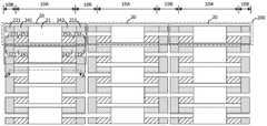
参考图4,半导体控温组件200包括多个基板100上且沿x方向排列的半导体控温单元20,半导体控温单元20包括热端电极21、P端电极22、N端电极23、P型半导体24和N型半导体25,P型半导体24连接P端电极22和热端电极21,N型半导体25连接N端电极23和热端电极21。其工作原理是P型半导体24和N型半导体25联结成为一个热电偶,形成一个P-N结,当有直流电通过这个P-N结时,由于温差电势的存在,就会产生能量的转移。热端电极21位于温度较高一端,P端电极22、N端电极23位于温度较低的一端,电流在各电极和半导体中运动,使得热端电极21的热量向P端电极22、N端电极23转移,最终达到平衡。由于热端电极21设于各形变区10A,P端电极22、N端电极23设于各节点区10B,因此会使形变区10A产生的热量向节点区10B转移,最终使基板100整体热量分布均匀,避免因局部热量过高影响共振效率与共振峰,确保了触觉模拟的准确性。需要说明的是,P型半导体24和N型半导体25分别连接形变区10A和节点区10B的电极,其位置根据电极的大小不同而不同,可能位于形变区10A,也可能位于节点区10B,还可能跨过这两个区域。Referring to FIG. 4 , the semiconductor
另一方面,由于上述热量转移是在直流电的驱动下进行,控制电流大小即可实现对热量转移情况的控制,进而实现对温度的控制。由于手指接触的区域为形变区10A,可以根据该原理可控制形变区10A的温度与升降温变化,模拟不同介面比热与热导率不同产生的温觉效应,实现不同温觉的触觉感知,提高触觉再现技术的丰富性。On the other hand, since the above-mentioned heat transfer is carried out under the driving of direct current, the control of the heat transfer can be realized by controlling the magnitude of the current, thereby realizing the control of the temperature. Since the area touched by the finger is the
再一方面,形变区10A内波峰或波谷位置为温度最高点,节点区10B为温度最低点,波峰或波谷位置到节点区10B的距离为振动波长的1/4。由于触觉感受的半波长需不超过20mm,因此高低温距离差最大可为10mm,也就是说,波峰或波谷位置到节点区10B的距离最大可为10mm。由于本发明的半导体控温单元20为水平设置,因此完全可以对较大形变的基板100进行控温,避免因热量引起共振锋偏移。同时可以透过外加电源/电容器,实现正负Thomson效应。On the other hand, the position of the wave crest or trough in the
本发明中,如图所示,半导体控温组件200可以设置在基板100上方,以半导体控温组件200背离基板100的一面为手指触摸面。半导体控温组件200也可以设置在基板100下方,以基板100背离半导体控温组件200的一面作为手指触摸面。另外,半导体控温组件200和振动源可以设置在基板100的同一面,也可以设置在不同面。In the present invention, as shown in the figure, the semiconductor
下面以图1所示的振动形态为例,以半导体控温组件200设置在基板100上方为例,对本发明实施方式的触觉再现装置进行详细说明:Taking the vibration form shown in FIG. 1 as an example, and taking the semiconductor
图4所示为第一种实施方式中的半导体控温组件200的俯视示意图,本实施方式中,x方向上示意性的示出了三个半导体控温单元20,以对基板100在x方向上各形变区10A温度进行均衡。以一个半导体控温单元20为例,半导体控温单元20包括热端电极21、P端电极22、N端电极23、P型半导体24和N型半导体25,P型半导体24连接P端电极22和热端电极21,N型半导体25连接N端电极23和热端电极21。本实施方式中,半导体控温单元20是非对称的结构,例如每个半导体控温单元20只有左侧的P端电极22、N端电极23,可以理解的是,P端电极22、N端电极23也可以位于热端电极右侧。FIG. 4 is a schematic top view of the semiconductor
图5所示为第二种实施方式中半导体控温组件200的俯视示意图,图6是图5中A-A处的截面示意图,半导体控温单元20为左右对称的结构,P端电极22包括第一P端电极221和第二P端电极222,N端电极23包括第一N端电极231和第二N端电极232,P型半导体24包括第一P型半导体241和第二P型半导体242,N型半导体25包括第一N型半导体251和第二N型半导体252。FIG. 5 is a schematic top view of the semiconductor
结合图5和图6,以一个半导体控温单元20为例,热端电极21位于一个形变区10A,第一P端电极221和第一N端电极231位于热端电极21左侧的节点区10B,第一P型半导体241连接第一P端电极221和热端电极21,第一N型半导体251连接第一N端电极231和热端电极21;第二P端电极222和第二N端电极232位于热端电极21右侧的节点区10B,第二P型半导体242连接第二P端电极222和热端电极21,第二N型半导体252连接第二N端电极232和热端电极21。该对称结构半导体控温单元20左右两部分均可以进行热量转移,即中间形变区10A的热量可以分别向左右两侧的节点区10B转移,以提高温度均衡的速率。5 and 6 , taking a semiconductor
在x方向上,由于相邻的两个半导体控温单元20都是对称结构,因此,其中一个半导体控温单元20中的第一P端电极221、第一N端电极231和另一个半导体控温单元20中的第二P端电极222、第二N端电极232位于同一个节点区10B。在本实施例所示的结构中,位于同一个节点区10B的第一P端电极221和第二P端电极222各自独立,位于同一个节点区10B的第一N端电极231和第二N端电极232各自独立。In the x-direction, since the two adjacent semiconductor
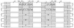
图7所示为第三种实施方式中的半导体控温组件200的结构示意图,与图5不同的是,在本实施方式中,位于同一个节点区10B的第一P端电极221和第二P端电极222连接为一体,位于同一个节点区10B的第一N端电极231和第二N端电极232连接为一体。FIG. 7 is a schematic structural diagram of the semiconductor
上述三个实施方式中,半导体控温组件200的数量均为多个,多个半导体控温组件200沿y方向排列,即所有的半导体控温单元20呈阵列排布,以此可以对整个基板100都进行散热。在y方向上相邻的两个半导体控温单元20中,一个半导体控温单元20中的第一P端电极221和另一个半导体控温单元20中的第一N端电极231连接为一体,一个半导体控温单元20中的第二P端电极222和另一个半导体控温单元20中的第二N端电极232连接为一体,由此使得y方向的半导体控温单元20串联在一起,所有的半导体控温单元20覆盖在整个基板100上,对基板100各位置都进行散热和均温,使得整个基板100的温度都能够实现均衡。In the above three embodiments, the number of semiconductor
半导体控温单元20需要与电源连接。对于一个半导体控温单元20而言,电源正极与N端电极23连接,负极与P端电极22连接。当半导体控温单元20阵列排布时,有多种连接电源的方式,均可以实现热量转移。图8-图10示出了不同结构半导体控温组件200与电源不同连接方式的示意图。The semiconductor
如图8所示,以图5结构的半导体控温组件200为例,每个半导体控温单元20的第一N端电极231、第一P端电极221可以单独连接一个电源的正负极,对称的另一侧的第二N端电极232、第二P端电极222可以单独连接一个电源的正负极。As shown in FIG. 8 , taking the semiconductor
如图9所示,继续以图5结构的半导体控温组件200为例,y方向上的所有半导体控温单元20左侧的N端电极23和P端电极22可以串联连接一个电源,即第一个第一N端电极231连接电源正极,最后一个第一P端电极221连接电源负极。对称的另一侧的N端电极23和P端电极22也串联连接在同一个电源上。As shown in FIG. 9, continuing to take the semiconductor
如图10所示,以图7结构的半导体控温组件200为例,在x方向上,位于同一个节点区10B的第一P端电极221、第二P端电极222连接、第一N端电极231、第二N端电极232连接为一个整体电极时,y方向上各相邻的整体电极的一端可连接在一个电源的正极,另一端连接另一个电源的负极。As shown in FIG. 10 , taking the semiconductor
本发明实施方式中,由于热端电极21设置于形变区10A,占用面积较大,为了不影响显示画面,实现视觉效果,优选采用透明电极。具体材料可以为半导体氧化铟锡(ITO)或石墨烯等。P端电极、N端电极仅位于节点区10B,面积较小,可以采用金属电极。金属电极的材料可以是一种金属,也可以是多种金属组成的合金,还可以由多种金属膜层形成,如Ni、Cu、Au形成的三层膜结构,其电阻较低,导热效果好,厚度可以设置为500nm-3μm。In the embodiment of the present invention, since the
触觉再现装置还包括导热层300,参考图11和图12,图11示出了包含导热层300的触觉再现装置的俯视图,图12为图11中B-B处的截面示意图,导热层300设于热端电极21背离基板100的一侧,此时,手指接触的面为导热层300背离基板100的一面。导热层300采用导热材料制作,例如可以为氮化铝、氮化硼、碳化硅、氧化镁、氧化铝等。导热层300至少覆盖形变区10A,起到大面积热传作用,避免表面温度积累,提高热平衡效率。在本实施方式中,导热层300上设有开口310,开口310暴露出下方的P端电极22和N端电极23,以便于与外部电源线连接。图中仅示出了一种开口形式,开口还可以是其他形式,本发明不对此进行特殊限定。The tactile reproduction device further includes a thermally
在一种实施方式中,参考图13,导热层300背离基板100一侧的表面为凹凸不平的表面,由此可以提高导热层300的表面积,实现散热,另一方面当导热层300为手指接触面时,凹凸不平的表面还能增加触觉接触面积或表面粗躁度的变化,更进一步提升触觉特性。如图所示,凹凸不平的表面可以为均匀分布有多个凸起的表面,凸起可以是规则或不规则的排布,凸起的形状可以是如图所示的矩形,还可以是锥形、圆形等其他任意形状。制作该结构的导热层300时,可以先通过流延工艺(tape casting)形成一整面的结构,然后使用等离子刻蚀搭配掩膜板进行刻蚀,也可使用曝光显影后的光刻胶作为掩模进行刻蚀,当然也可以采用其他方式进行制作,本申请不对具体工艺进行特殊限定。In one embodiment, referring to FIG. 13 , the surface of the thermally
在另一种实施方式中,参考图14,当手指接触面为基板100背离导热层300的一面时,半导体控温组件200设置在基板100下方,导热层300设于半导体控温组件200背离基板100的一侧。想要提高散热与增加触觉接触面积或表面粗躁度的变化,也可以通过在基板100背面形成凹凸不平的表面来实现。基板100背面凹凸不平的表面结构与导热层300表面的结构相似,此处不再赘述。In another embodiment, referring to FIG. 14 , when the finger contact surface is the side of the
以上实施方式中对图1所示的振动形式下半导体控温组件的结构设计进行了描述,对于图3所示的其他振动形式,半导体控温组件同样可以参考图4、5、7所示的结构,在各形变区和节点区设置半导体控温单元。可以理解的是,在图3所示的实施方式中,x方向是指远离圆心的任意方向,即任意半径所在的径向方向,y方向为环绕圆心的方向,即周向。另外,靠近圆心处的控温单元宽度较窄,远离圆心处的控温单元宽度较宽,以此覆盖更多的面积,实现良好的散热。In the above embodiments, the structural design of the semiconductor temperature control assembly in the vibration form shown in FIG. 1 is described. For other vibration forms shown in FIG. 3 , the semiconductor temperature control assembly can also refer to those shown in FIGS. structure, and a semiconductor temperature control unit is arranged in each deformation region and node region. It can be understood that, in the embodiment shown in FIG. 3 , the x direction refers to any direction away from the center of the circle, that is, the radial direction where any radius is located, and the y direction refers to the direction surrounding the center of the circle, that is, the circumferential direction. In addition, the width of the temperature control unit near the center of the circle is narrow, and the width of the temperature control unit far from the center of the circle is wider, so as to cover more area and achieve good heat dissipation.
本发明实施方式还提供一种显示面板,如图15所示,包括相对设置的背板500和盖板600,以及设于背板500和盖板600之间发光器件700,图中所示的发光器件700为OLED发光器件700,包括设置在像素界定层开口区的阳极层、有机发光功能层和阴极层,OLED发光器件700被封装层封装保护。OLED发光器件700上方即为盖板600。本实施方式中触觉再现装置的基板100即为图中的盖板600,也就是说,半导体控温组件200和振动源都设置在盖板600上,使得显示面板除了能显示画面,还能具有触觉再现的功能。由于热端电极21可采用透明电极,因此不会对面板显示造成影响。An embodiment of the present invention further provides a display panel, as shown in FIG. 15 , comprising a
半导体控温组件200可以设置在盖板600朝向背板500的一侧,也可以设置在背离背板500的一侧。当半导体控温组件200设置在盖板600朝向背板500的一侧,手指触摸面为盖板600的表面,当半导体控温组件200设置在盖板600背离背板500的一侧,手指触摸面为半导体控温组件200的表面。两种方式都可以对盖板600进行散热。The semiconductor
在一种实施方式中,显示面板为触控显示面板,其包括设置在盖板600上的触控膜层,触控膜层包含触控电极,当半导体控温组件200设置在盖板600朝向背板500的一侧时,半导体控温组件200的热端电极21可以复用为触控电极,由此使得盖板600同时作为触控显示面和触觉感受面。In one embodiment, the display panel is a touch display panel, which includes a touch film layer disposed on the
本发明实施方式还提供一种显示装置,包括上述显示面板。因此,也具有上述技术效果。Embodiments of the present invention further provide a display device including the above-mentioned display panel. Therefore, the above-mentioned technical effect is also obtained.
本发明对于显示装置的适用不做具体限制,其可以是电视机、笔记本电脑、平板电脑、可穿戴显示设备、手机、电子书、等任何具有显示功能的产品或部件。The present invention does not specifically limit the application of the display device, which can be any product or component with a display function, such as a TV set, a notebook computer, a tablet computer, a wearable display device, a mobile phone, an e-book, and the like.
以上实施方式以应用于显示领域进行了介绍,本发明对于压电陶瓷芯片组件的适用不做具体限制,其可以应用于显示装置中,以实现显示和触觉再现的结合,也还可以应用于实验设备、检测设备等其他领域中。The above embodiments are introduced in the field of display. The application of the present invention to the piezoelectric ceramic chip assembly is not specifically limited. It can be applied to a display device to realize the combination of display and tactile reproduction, and can also be applied to experiments. equipment, testing equipment and other fields.
虽然本说明书中使用相对性的用语,例如“上”“下”来描述图标的一个组件对于另一组件的相对关系,但是这些术语用于本说明书中仅出于方便,例如根据附图中所述的示例的方向。能理解的是,如果将图标的装置翻转使其上下颠倒,则所叙述在“上”的组件将会成为在“下”的组件。当某结构在其它结构“上”时,有可能是指某结构一体形成于其它结构上,或指某结构“直接”设置在其它结构上,或指某结构通过另一结构“间接”设置在其它结构上。Although relative terms such as "upper" and "lower" are used in this specification to describe the relative relationship of one component of an icon to another component, these terms are used in this specification only for convenience, such as according to the direction of the example described. It will be appreciated that if the device of the icon is turned upside down, the components described as "on" will become the components on "bottom". When a certain structure is "on" other structures, it may mean that a certain structure is integrally formed on other structures, or that a certain structure is "directly" arranged on other structures, or that a certain structure is "indirectly" arranged on another structure through another structure. other structures.
用语“一个”、“一”、“该”、“所述”和“至少一个”用以表示存在一个或多个要素/组成部分/等;用语“包括”和“具有”用以表示开放式的包括在内的意思并且是指除了列出的要素/组成部分/等之外还可存在另外的要素/组成部分/等。The terms "a", "an", "the", "said" and "at least one" are used to indicate the presence of one or more elements/components/etc; the terms "include" and "have" are used to indicate an open-ended Inclusive means and means that additional elements/components/etc may be present in addition to the listed elements/components/etc.
本领域技术人员在考虑说明书及实践这里公开的发明后,将容易想到本发明的其它实施方案。本申请旨在涵盖本发明的任何变型、用途或者适应性变化,这些变型、用途或者适应性变化遵循本发明的一般性原理并包括本发明未公开的本技术领域中的公知常识或惯用技术手段。说明书和实施例仅被视为示例性的,本发明的真正范围和精神由所附的权利要求指出。Other embodiments of the invention will readily occur to those skilled in the art upon consideration of the specification and practice of the invention disclosed herein. This application is intended to cover any variations, uses or adaptations of the invention which follow the general principles of the invention and which include common knowledge or conventional techniques in the art not disclosed by the invention . The specification and examples are to be regarded as exemplary only, with the true scope and spirit of the invention being indicated by the appended claims.
Claims (15)
Priority Applications (2)
| Application Number | Priority Date | Filing Date | Title |
|---|---|---|---|
| CN202011333604.XACN114546101B (en) | 2020-11-24 | 2020-11-24 | Tactile reproduction device, display panel, and display device |
| US17/489,632US11600549B2 (en) | 2020-11-24 | 2021-09-29 | Tactile representation device, display panel and display device |
Applications Claiming Priority (1)
| Application Number | Priority Date | Filing Date | Title |
|---|---|---|---|
| CN202011333604.XACN114546101B (en) | 2020-11-24 | 2020-11-24 | Tactile reproduction device, display panel, and display device |
Publications (2)
| Publication Number | Publication Date |
|---|---|
| CN114546101Atrue CN114546101A (en) | 2022-05-27 |
| CN114546101B CN114546101B (en) | 2024-05-17 |
Family
ID=81658588
Family Applications (1)
| Application Number | Title | Priority Date | Filing Date |
|---|---|---|---|
| CN202011333604.XAActiveCN114546101B (en) | 2020-11-24 | 2020-11-24 | Tactile reproduction device, display panel, and display device |
Country Status (2)
| Country | Link |
|---|---|
| US (1) | US11600549B2 (en) |
| CN (1) | CN114546101B (en) |
Cited By (2)
| Publication number | Priority date | Publication date | Assignee | Title |
|---|---|---|---|---|
| CN115359736A (en)* | 2022-09-23 | 2022-11-18 | 武汉天马微电子有限公司 | Display module and display device |
| CN118675419A (en)* | 2024-05-29 | 2024-09-20 | 昆山国显光电有限公司 | Temperature control assembly and display device |
Citations (7)
| Publication number | Priority date | Publication date | Assignee | Title |
|---|---|---|---|---|
| CN102129952A (en)* | 2010-01-12 | 2011-07-20 | 上海微电子装备有限公司 | Cooling devices and concentrators for high-pressure gas discharge lamps |
| CN102331800A (en)* | 2011-05-18 | 2012-01-25 | 东南大学 | A multi-heat source temperature tactile reproduction device |
| CN104063054A (en)* | 2014-06-06 | 2014-09-24 | 南京航空航天大学 | Tactile reproduction device and tactile reproduction method based on two-way friction force control |
| CN104331155A (en)* | 2014-10-27 | 2015-02-04 | 北京理工大学 | Device using electric stimulation to realize touch reappearing |
| RU161159U1 (en)* | 2015-04-06 | 2016-04-10 | Александр Иванович Грядунов | DEVICE FOR MAINTAINING HUMAN ACTIVE PERFORMANCE |
| CN106708262A (en)* | 2016-12-08 | 2017-05-24 | 苏州欧菲光科技有限公司 | Electronic equipment and tactile feedback device thereof |
| CN108461617A (en)* | 2018-02-08 | 2018-08-28 | 南方科技大学 | Temperature regulation device and preparation method |
Family Cites Families (2)
| Publication number | Priority date | Publication date | Assignee | Title |
|---|---|---|---|---|
| TWI714319B (en)* | 2019-10-28 | 2020-12-21 | 錼創顯示科技股份有限公司 | Micro light-emitting diode device |
| TWI757904B (en)* | 2020-10-06 | 2022-03-11 | 友達光電股份有限公司 | Electronic device |
- 2020
- 2020-11-24CNCN202011333604.XApatent/CN114546101B/enactiveActive
- 2021
- 2021-09-29USUS17/489,632patent/US11600549B2/enactiveActive
Patent Citations (7)
| Publication number | Priority date | Publication date | Assignee | Title |
|---|---|---|---|---|
| CN102129952A (en)* | 2010-01-12 | 2011-07-20 | 上海微电子装备有限公司 | Cooling devices and concentrators for high-pressure gas discharge lamps |
| CN102331800A (en)* | 2011-05-18 | 2012-01-25 | 东南大学 | A multi-heat source temperature tactile reproduction device |
| CN104063054A (en)* | 2014-06-06 | 2014-09-24 | 南京航空航天大学 | Tactile reproduction device and tactile reproduction method based on two-way friction force control |
| CN104331155A (en)* | 2014-10-27 | 2015-02-04 | 北京理工大学 | Device using electric stimulation to realize touch reappearing |
| RU161159U1 (en)* | 2015-04-06 | 2016-04-10 | Александр Иванович Грядунов | DEVICE FOR MAINTAINING HUMAN ACTIVE PERFORMANCE |
| CN106708262A (en)* | 2016-12-08 | 2017-05-24 | 苏州欧菲光科技有限公司 | Electronic equipment and tactile feedback device thereof |
| CN108461617A (en)* | 2018-02-08 | 2018-08-28 | 南方科技大学 | Temperature regulation device and preparation method |
Cited By (3)
| Publication number | Priority date | Publication date | Assignee | Title |
|---|---|---|---|---|
| CN115359736A (en)* | 2022-09-23 | 2022-11-18 | 武汉天马微电子有限公司 | Display module and display device |
| CN115359736B (en)* | 2022-09-23 | 2023-11-21 | 武汉天马微电子有限公司 | Display assembly and display device |
| CN118675419A (en)* | 2024-05-29 | 2024-09-20 | 昆山国显光电有限公司 | Temperature control assembly and display device |
Also Published As
| Publication number | Publication date |
|---|---|
| CN114546101B (en) | 2024-05-17 |
| US11600549B2 (en) | 2023-03-07 |
| US20220165642A1 (en) | 2022-05-26 |
Similar Documents
| Publication | Publication Date | Title |
|---|---|---|
| US10749144B2 (en) | Display substrate and method for preparing the same, and display device | |
| CN106293244B (en) | Touch-control display panel and its driving method and touch control display apparatus | |
| TWI408441B (en) | Touch display panel and touch substrate | |
| CN101320766B (en) | Current spreading layer, light emitting diode device and manufacturing method thereof | |
| JP5795291B2 (en) | Touch sensing electrode and touch panel | |
| CN203299774U (en) | Touch panel and touch display panel | |
| CN114546101B (en) | Tactile reproduction device, display panel, and display device | |
| CN103376966A (en) | Electrostatic capacity type touch screen panel for display device and method of manufacturing the same | |
| KR20110133840A (en) | Touch panel | |
| CN204539691U (en) | Heat radiation module with high and low surface combined with mobile device | |
| JP2013004074A (en) | Capacitive touch panel | |
| US11393959B2 (en) | Micro light-emitting diode device | |
| CN111971645A (en) | Shape-changeable electronic device and operation method thereof | |
| CN105702701A (en) | Piezoelectric touch organic light-emitting display panel and manufacturing method thereof, and organic light-emitting display | |
| CN117222197A (en) | Display modules and electronic equipment | |
| CN109739382A (en) | Touch Devices and Display Devices | |
| TW202016713A (en) | Touch module | |
| CN115000117B (en) | Array substrate and display panel | |
| CN110729339A (en) | Organic light emitting diode display device and manufacturing method thereof | |
| CN206821132U (en) | A portable device with heat dissipation structure | |
| CN101424989A (en) | Touch input device and electronic system comprising same | |
| CN114967234B (en) | Display backplane, adjustment method and display device thereof | |
| CN105282961B (en) | Electronic substrate heat radiation structure | |
| TWI543039B (en) | Flat heater | |
| CN112817480B (en) | Touch display module and display device |
Legal Events
| Date | Code | Title | Description |
|---|---|---|---|
| PB01 | Publication | ||
| PB01 | Publication | ||
| SE01 | Entry into force of request for substantive examination | ||
| SE01 | Entry into force of request for substantive examination | ||
| GR01 | Patent grant | ||
| GR01 | Patent grant |