CN114545532A - Mask-embedded microlens array and method of use - Google Patents
Mask-embedded microlens array and method of useDownload PDFInfo
- Publication number
- CN114545532A CN114545532ACN202011291940.2ACN202011291940ACN114545532ACN 114545532 ACN114545532 ACN 114545532ACN 202011291940 ACN202011291940 ACN 202011291940ACN 114545532 ACN114545532 ACN 114545532A
- Authority
- CN
- China
- Prior art keywords
- microlens array
- mask
- microlens
- embedded
- mask layer
- Prior art date
- Legal status (The legal status is an assumption and is not a legal conclusion. Google has not performed a legal analysis and makes no representation as to the accuracy of the status listed.)
- Pending
Links
Images


Classifications
- G—PHYSICS
- G02—OPTICS
- G02B—OPTICAL ELEMENTS, SYSTEMS OR APPARATUS
- G02B3/00—Simple or compound lenses
- G02B3/0006—Arrays
- G—PHYSICS
- G02—OPTICS
- G02B—OPTICAL ELEMENTS, SYSTEMS OR APPARATUS
- G02B3/00—Simple or compound lenses
- G02B3/0006—Arrays
- G02B3/0037—Arrays characterized by the distribution or form of lenses
Landscapes
- Physics & Mathematics (AREA)
- General Physics & Mathematics (AREA)
- Optics & Photonics (AREA)
- Optical Elements Other Than Lenses (AREA)
Abstract
Translated fromChinese
Description
Translated fromChinese技术领域technical field
本发明涉及深度相机,具体地,涉及一种内嵌掩模的微透镜阵列及使用方法。The present invention relates to a depth camera, in particular, to a microlens array embedded in a mask and a method of using the same.
背景技术Background technique
微透镜阵列是由通光孔径及浮雕深度为微米级的透镜组成的阵列,它不仅具有传统透镜的聚焦、成像等基本功能,而且具有单元尺寸小、集成度高的特点,使得它能够完成传统光学元件无法完成的功能,并能构成许多新型的光学系统。The microlens array is an array composed of lenses with a clear aperture and a relief depth of micrometers. It not only has the basic functions of traditional lenses such as focusing and imaging, but also has the characteristics of small unit size and high integration. Optical components can not complete the function, and can form many new optical systems.
微透镜阵列可分为折射型微透镜阵列与衍射型微透镜阵列两类。衍射微透镜列阵利用其表面波长量级的三维浮雕结构对光波进行调制、变换,具有轻而薄、设计灵活等特点。作为功能元件,在波前传感、光聚能、光整形等多种系统可得到广泛应用。Microlens arrays can be divided into two types: refractive microlens arrays and diffractive microlens arrays. The diffractive microlens array modulates and transforms the light wave by using the three-dimensional relief structure of the surface wavelength magnitude, and has the characteristics of lightness, thinness and flexible design. As a functional element, it can be widely used in various systems such as wavefront sensing, light concentrating, and light shaping.
微透镜阵列系统广泛应用于光学成像,光学非成像系统及其他光学系统中,能通过表面微结构实现光束整形,高频率波等功能。然而受限于微结构,光束聚焦往往伴随着像差和次级衍射,如向外投射散斑状结构光时,平行光入射单个透镜会汇聚成一点,但是当微透镜孔径较小时,衍射效应会变得明显。当有衍射和像差存在时,平行光束会在焦平面形成弥散圆,影响整个散点图的对比度,不利于后续算法的处理。Microlens array systems are widely used in optical imaging, optical non-imaging systems and other optical systems, and can realize beam shaping and high-frequency wave functions through surface microstructures. However, limited by the microstructure, beam focusing is often accompanied by aberration and secondary diffraction. For example, when speckle structured light is projected outward, the parallel light incident on a single lens will converge to a point, but when the aperture of the microlens is small, the diffraction effect will become apparent. When there is diffraction and aberration, the parallel beam will form a circle of confusion in the focal plane, which will affect the contrast of the entire scattergram, which is not conducive to the processing of subsequent algorithms.
发明内容SUMMARY OF THE INVENTION
针对现有技术中的缺陷,本发明的目的是提供一种内嵌掩模的微透镜阵列及使用方法。In view of the defects in the prior art, the purpose of the present invention is to provide a microlens array with a built-in mask and a method for using the same.
根据本发明提供的内嵌掩模的微透镜阵列,包括基板、无机层、掩膜层以及微透镜阵列;The mask-embedded microlens array provided according to the present invention includes a substrate, an inorganic layer, a mask layer and a microlens array;
所述基板的一侧面上形成所述无机层,所述无机层上与所述基板相背离的一侧面上形成所述掩膜层;所述掩膜层上与所述基板相背离的一侧面上形成所述微透镜阵列;The inorganic layer is formed on one side of the substrate, the mask layer is formed on the side of the inorganic layer away from the substrate; the mask layer is formed on the side away from the substrate forming the microlens array on it;
所述掩膜层上的镂空与所述微透镜阵列上的微透镜一一对应;所述掩模层位于所述微透镜阵列入射光方向的焦点深度位置。The hollows on the mask layer correspond one-to-one with the microlenses on the microlens array; the mask layer is located at the focal depth position of the incident light direction of the microlens array.
优选地,所述镂空为圆形,所述镂空的直径A与所述微透镜的焦距和通光孔径之间的关系,需满足如下条件式:Preferably, the hollow is circular, and the relationship between the diameter A of the hollow and the focal length and clear aperture of the microlens must satisfy the following conditional formula:

其中,λ为入射光的波长,f为微透镜的焦距,d为微透镜的通光孔径。Among them, λ is the wavelength of the incident light, f is the focal length of the microlens, and d is the clear aperture of the microlens.
优选地,所述微透镜的厚度与所述微透镜的焦距相等。Preferably, the thickness of the microlens is equal to the focal length of the microlens.
优选地,每一所述微透镜与对应镂空之间的对准偏差不超所述镂空直径的10%。Preferably, the alignment deviation between each of the microlenses and the corresponding hollow does not exceed 10% of the diameter of the hollow.
优选地,所述微透镜阵列中微透镜排列方式包括满铺式和非满铺式;Preferably, the arrangement of the microlenses in the microlens array includes a full-coverage type and a non-full-coverage type;
所述满铺式为相邻的微透镜之间不具有间隙,所述非满铺式为相邻的微透镜之间具有间隙。The full-coverage type means that there are no gaps between adjacent microlenses, and the non-full-coverage type means that there are gaps between adjacent microlenses.
优选地,所述微透镜的曲面面型为非球面,每一所述微透镜的曲面面型公式z为:Preferably, the curved surface type of the microlenses is aspherical, and the curved surface type formula z of each of the microlenses is:

其中,c是曲面的曲率,r是微透镜的径向坐标,k是圆锥系数。where c is the curvature of the surface, r is the radial coordinate of the microlens, and k is the conic coefficient.
优选地,所述无机层采用二氧化硅层。Preferably, the inorganic layer is a silicon dioxide layer.
优选地,所述基板采用光学玻璃或光学塑料。Preferably, the substrate is made of optical glass or optical plastic.
优选地,所述微透镜阵列的排布方式包括三角形、四边形、六边形以及八边形中的任一形状。Preferably, the arrangement of the microlens array includes any shape of triangle, quadrangle, hexagon and octagon.
根据本发明提供的的内嵌掩模的微透镜阵列的使用方法,包括如下步骤:According to the method for using the microlens array embedded in the mask provided by the present invention, the method includes the following steps:
将多束准直光束入射所述微透镜阵列;injecting multiple collimated light beams into the microlens array;
所述微透镜阵列使得所述准直光束聚焦于所述掩模层的镂空内,以通过所述掩模层进行次级衍射光和杂散光的过滤;The microlens array makes the collimated light beam focus in the hollow of the mask layer, so as to filter the secondary diffracted light and stray light through the mask layer;
过滤后的所述准直光束从基板中出射。The filtered collimated beam emerges from the substrate.
与现有技术相比,本发明具有如下的有益效果:Compared with the prior art, the present invention has the following beneficial effects:
本发明中在基板的一侧面上形成掩膜层,在掩膜层上与基板相背离的一侧面上形成所述微透镜阵列,同时控制连续微透镜表面的面型,能够使得经过微透镜阵列系统的光束得到约束,有效地过滤掉次级衍射和杂散光,进而提高有效光的利用率,提高了散斑状结构光投射后中光斑点的对比度,便于在光斑点图像中进行光斑点的提取。In the present invention, a mask layer is formed on one side of the substrate, and the microlens array is formed on the side of the mask layer away from the substrate. At the same time, the surface shape of the continuous microlens surface is controlled, so that the microlens array can pass through the microlens array. The beam of the system is constrained, and the secondary diffraction and stray light are effectively filtered out, thereby improving the utilization rate of the effective light, improving the contrast of the light spot after the speckle structured light is projected, and facilitating the extraction of the light spot in the light spot image. .
附图说明Description of drawings
为了更清楚地说明本发明实施例或现有技术中的技术方案,下面将对实施例或现有技术描述中所需要使用的附图作简单地介绍,显而易见地,下面描述中的附图仅仅是本发明的实施例,对于本领域普通技术人员来讲,在不付出创造性劳动的前提下,还可以根据提供的附图获得其他的附图。通过阅读参照以下附图对非限制性实施例所作的详细描述,本发明的其它特征、目的和优点将会变得更明显:In order to explain the embodiments of the present invention or the technical solutions in the prior art more clearly, the following briefly introduces the accompanying drawings that need to be used in the description of the embodiments or the prior art. Obviously, the accompanying drawings in the following description are only It is an embodiment of the present invention. For those of ordinary skill in the art, other drawings can also be obtained according to the provided drawings without creative work. Other features, objects and advantages of the present invention will become more apparent by reading the detailed description of non-limiting embodiments with reference to the following drawings:
图1为本发明实施例中内嵌掩模的微透镜阵列的结构示意图;1 is a schematic structural diagram of a microlens array with an embedded mask in an embodiment of the present invention;
图2(a)为本发明实施例中微透镜阵列满铺式排列的示意图;Fig. 2 (a) is the schematic diagram of the microlens array full-covered arrangement in the embodiment of the present invention;
图2(b)为本发明实施例中微透镜阵列非满铺式排列的示意图;FIG. 2(b) is a schematic diagram of a non-covered arrangement of microlens arrays in an embodiment of the present invention;
图3为本发明实施例中基板上掩模层侧视图与顶视图的对应示意图;3 is a corresponding schematic diagram of a side view and a top view of a mask layer on a substrate in an embodiment of the present invention;
图4为本发明实施例中内嵌掩模的微透镜阵列生成散斑状结构光的单点光路示意图;4 is a schematic diagram of a single-point optical path for generating speckle-shaped structured light by a microlens array embedded with a mask in an embodiment of the present invention;
图5为本发明实施例中内嵌掩模的微透镜阵列的使用步骤示意图。FIG. 5 is a schematic diagram of the steps of using the microlens array embedded in the mask according to the embodiment of the present invention.
图中:In the picture:
1为基板;2为无机层;3为掩膜层;4为微透镜阵列;5为虚焦点。1 is the substrate; 2 is the inorganic layer; 3 is the mask layer; 4 is the microlens array; 5 is the virtual focus.
具体实施方式Detailed ways
下面结合具体实施例对本发明进行详细说明。以下实施例将有助于本领域的技术人员进一步理解本发明,但不以任何形式限制本发明。应当指出的是,对本领域的普通技术人员来说,在不脱离本发明构思的前提下,还可以做出若干变形和改进。这些都属于本发明的保护范围。The present invention will be described in detail below with reference to specific embodiments. The following examples will help those skilled in the art to further understand the present invention, but do not limit the present invention in any form. It should be noted that, for those skilled in the art, several modifications and improvements can be made without departing from the concept of the present invention. These all belong to the protection scope of the present invention.
需要说明的是,当元件被称为“固定于”或“设置于”另一个元件,它可以直接在另一个元件上或者间接在该另一个元件上。当一个元件被称为是“连接于”另一个元件,它可以是直接连接到另一个元件或间接连接至该另一个元件上。另外,连接即可以是用于固定作用也可以是用于电路连通作用。It should be noted that when an element is referred to as being "fixed to" or "disposed on" another element, it can be directly on the other element or indirectly on the other element. When an element is referred to as being "connected to" another element, it can be directly connected to the other element or indirectly connected to the other element. In addition, the connection can be used for either a fixing function or a circuit connecting function.
需要理解的是,术语“长度”、“宽度”、“上”、“下”、“前”、“后”、“左”、“右”、“竖直”、“水平”、“顶”、“底”“内”、“外”等指示的方位或位置关系为基于附图所示的方位或位置关系,仅是为了便于描述本发明实施例和简化描述,而不是指示或暗示所指的装置或元件必须具有特定的方位、以特定的方位构造和操作,因此不能理解为对本发明的限制。It is to be understood that the terms "length", "width", "upper", "lower", "front", "rear", "left", "right", "vertical", "horizontal", "top" , "bottom", "inside", "outside", etc. indicate the orientation or positional relationship based on the orientation or positional relationship shown in the accompanying drawings, which are only for the convenience of describing the embodiments of the present invention and simplifying the description, rather than indicating or implying that The device or element must have a specific orientation, be constructed and operated in a specific orientation, and therefore should not be construed as a limitation of the present invention.
此外,术语“第一”、“第二”仅用于描述目的,而不能理解为指示或暗示相对重要性或者隐含指明所指示的技术特征的数量。由此,限定有“第一”、“第二”的特征可以明示或者隐含地包括一个或者更多该特征。在本发明实施例的描述中,“多个”的含义是两个或两个以上,除非另有明确具体的限定。In addition, the terms "first" and "second" are only used for descriptive purposes, and should not be construed as indicating or implying relative importance or implying the number of indicated technical features. Thus, a feature defined as "first", "second" may expressly or implicitly include one or more of that feature. In the description of the embodiments of the present invention, "plurality" means two or more, unless otherwise expressly and specifically defined.
在本发明中的内嵌掩模的微透镜阵列,包括基板、无机层、掩膜层以及微透镜阵列;The mask-embedded microlens array in the present invention includes a substrate, an inorganic layer, a mask layer and a microlens array;
所述基板的一侧面上形成所述无机层,所述无机层上与所述基板相背离的一侧面上形成所述掩膜层;所述掩膜层上与所述基板相背离的一侧面上形成所述微透镜阵列;The inorganic layer is formed on one side of the substrate, the mask layer is formed on the side of the inorganic layer away from the substrate; the mask layer is formed on the side away from the substrate forming the microlens array on it;
所述掩膜层上的镂空与所述微透镜阵列上的微透镜一一对应;所述掩模层位于所述微透镜阵列入射光方向的焦点深度位置。The hollows on the mask layer correspond one-to-one with the microlenses on the microlens array; the mask layer is located at the focal depth position of the incident light direction of the microlens array.
本发明实施例中在基板的一侧面上形成掩膜层,在掩膜层上与基板相背离的一侧面上形成所述微透镜阵列,同时控制连续微透镜表面的面型,能够使得经过微透镜阵列系统的光束得到约束,有效地过滤掉次级衍射和杂散光,进而提高有效光的利用率,提高了散斑状结构光投射后中光斑点的对比度,便于光斑图中光斑点的提取。In the embodiment of the present invention, a mask layer is formed on one side of the substrate, and the microlens array is formed on the side of the mask layer away from the substrate. The beam of the lens array system is constrained, which effectively filters out secondary diffraction and stray light, thereby improving the utilization rate of effective light, improving the contrast of light spots after the speckle structured light is projected, and facilitating the extraction of light spots in the speckle image.
以上是本发明的核心思想,为使本发明的上述目的、特征和优点能够更加明显易懂,下面将结合本发明实施例中的附图,对本发明实施例中的技术方案进行清楚、完整地描述,显然,所描述的实施例仅仅是本发明一部分实施例,而不是全部的实施例。基于本发明中的实施例,本领域普通技术人员在没有做出创造性劳动前提下所获得的所有其他实施例,都属于本发明保护的范围。The above is the core idea of the present invention. In order to make the above objects, features and advantages of the present invention more obvious and easy to understand, the technical solutions in the embodiments of the present invention will be clearly and completely described below with reference to the accompanying drawings in the embodiments of the present invention. Description, it is obvious that the described embodiments are only some, but not all, embodiments of the present invention. Based on the embodiments of the present invention, all other embodiments obtained by those of ordinary skill in the art without creative efforts shall fall within the protection scope of the present invention.
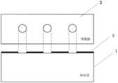
图1为本发明实施例中内嵌掩模的微透镜阵列的结构示意图,如图1所示,本发明提供的内嵌掩模的微透镜阵列,包括基板1、无机层2、掩膜层3以及微透镜阵列4;FIG. 1 is a schematic structural diagram of a mask-embedded microlens array according to an embodiment of the present invention. As shown in FIG. 1 , the mask-embedded microlens array provided by the present invention includes a
所述基板1的一侧面上形成所述无机层2,所述无机层2上与所述基板1相背离的一侧面上形成所述掩膜层3;所述掩膜层3上与所述基板1相背离的一侧面上形成所述微透镜阵列4;The
所述掩膜层3上的镂空与所述微透镜阵列4上的微透镜一一对应;所述掩模层位于所述微透镜阵列4入射光方向的焦点深度位置。The hollows on the
图3为本发明实施例中基板上掩模层侧视图与顶视图的对应示意图,如图3所示,所述镂空为圆形,所述镂空的直径A与所述微透镜的焦距和通光孔径之间的关系,需满足如下条件式:FIG. 3 is a corresponding schematic diagram of a side view and a top view of a mask layer on a substrate in an embodiment of the present invention. As shown in FIG. 3 , the hollow is a circle, and the diameter A of the hollow is related to the focal length and distance of the microlens. The relationship between the apertures needs to satisfy the following conditional formula:

其中,λ为入射光的波长,f为微透镜的焦距,d为微透镜的通光孔径。Among them, λ is the wavelength of the incident light, f is the focal length of the microlens, and d is the clear aperture of the microlens.
在本发明实施例中,掩模层的镂空直径不能过大或过小,当镂空直径过大时,非有效光会经过镂空透射出来,影响成像效果;当微透镜用于生成圆形光斑时,过多的杂光会影响光斑的对比度。当镂空圆形直径过小时,有效光会被遮挡,降低整个光学系统的光学效率。In the embodiment of the present invention, the hollow diameter of the mask layer cannot be too large or too small. When the hollow diameter is too large, ineffective light will be transmitted through the hollow, affecting the imaging effect; when the microlens is used to generate a circular light spot , too much stray light will affect the contrast of the spot. When the diameter of the hollow circle is too small, the effective light will be blocked, reducing the optical efficiency of the entire optical system.
在本发明实施例中,所述微透镜的厚度与所述微透镜的焦距相等,能够使微透镜焦点位置落在掩模层的同一深度。In the embodiment of the present invention, the thickness of the microlens is equal to the focal length of the microlens, so that the focal position of the microlens can fall at the same depth of the mask layer.
所述微透镜的制作方法如下:The manufacturing method of the microlens is as follows:
将设计镂空图案的掩模层形成之后,在掩模层的基础上镀上一层厚度与微透镜焦距相同的二氧化硅膜,在镀膜时精准控制微透镜的厚度。再通过压印,光刻或刻蚀方式对所镀膜层进行加工,得到与镂空图案匹配的微透镜阵列4。After the mask layer with the hollow pattern is formed, a silicon dioxide film with the same thickness as the focal length of the microlens is coated on the basis of the mask layer, and the thickness of the microlens is precisely controlled during coating. Then, the coated layer is processed by imprinting, photolithography or etching to obtain a
在本发明实施例中,每一所述微透镜与对应镂空之间的对准偏差不超所述镂空直径的10%。In the embodiment of the present invention, the alignment deviation between each of the microlenses and the corresponding hollow does not exceed 10% of the diameter of the hollow.
图2(a)为本发明实施例中微透镜阵列满铺式排列的示意图,图2(b)为本发明实施例中微透镜阵列非满铺式排列的示意图,如图2所示,所述微透镜阵列4中微透镜排列方式包括满铺式和非满铺式;FIG. 2(a) is a schematic diagram of a full-coverage arrangement of microlens arrays in an embodiment of the present invention, and FIG. 2(b) is a schematic diagram of a non-full-coverage arrangement of microlens arrays in an embodiment of the present invention. As shown in FIG. 2, the The microlens arrangement in the
如图2(a)所示,所述满铺式为相邻的微透镜之间不具有间隙,所述微透镜阵列4的整个入光面均为有效区域。如图2(b)所示,所述非满铺式为相邻的微透镜之间具有间隙。非满铺式中每个微透镜的通光孔径为圆形,微透镜间具有空隙,所述微透镜阵列4的有效区域仅为每个微透镜通光孔的圆形区域。As shown in FIG. 2( a ), the full-floor type means that there is no gap between adjacent microlenses, and the entire light incident surface of the
在本发明一实施例中,所述微透镜阵列4的排布方式包括三角形、四边形、六边形以及八边形中的任一形状。In an embodiment of the present invention, the arrangement of the
在本发明一实施例中,所述微透镜的曲面面型为非球面,每一所述微透镜的曲面面型公式z为:In an embodiment of the present invention, the curved surface of the microlens is aspherical, and the curved surface formula z of each of the microlenses is:

其中,c是曲面的曲率,r是微透镜的径向坐标,k是圆锥系数。其中,微透镜的曲率决定微透镜的焦距,微透镜的圆锥系数决定了在该曲率基础上对面型的调整。where c is the curvature of the surface, r is the radial coordinate of the microlens, and k is the conic coefficient. The curvature of the microlens determines the focal length of the microlens, and the conic coefficient of the microlens determines the adjustment of the face shape based on the curvature.
所述微透镜的曲面面型能够改善由于球面聚焦产生的非理想像点的尺寸和出射光线的球面度。The curved surface type of the microlens can improve the size of the non-ideal image point and the sphericity of the outgoing light due to spherical focusing.
在本发明一实施例中,所述无机层2采用二氧化硅层。二氧化硅层先于掩模层镀在基板1上,用于为金属制成的掩模层打底,提高掩模层的附着力,所述二氧化硅层也可以采用多种无机膜层制成。In an embodiment of the present invention, the
在本发明一实施例中,所述基板1采用光学玻璃或光学塑料。所述基板1具有韧性不易碎并且易于无机层2附着。In an embodiment of the present invention, the
图4为本发明实施例中内嵌掩模的微透镜阵列生成散斑状结构光的单点光路示意图,如图4所示,所述微透镜阵列4使得入射的所述准直光束聚焦于所述掩模层的镂空内,以通过所述掩模层进行次级衍射光和杂散光的过滤,从而提高了散斑状结构光投射后中光斑点的对比度,便于在光斑点图像中进行光斑点的提取。FIG. 4 is a schematic diagram of a single-point optical path for generating speckle structured light by a microlens array embedded with a mask in an embodiment of the present invention. As shown in FIG. 4 , the
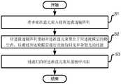
图5为本发明实施例中内嵌掩模的微透镜阵列的使用步骤示意图,如图5所示,本发明提供的所述的内嵌掩模的微透镜阵列的使用方法,包括如下步骤:5 is a schematic diagram of the steps of using the microlens array embedded in the mask in the embodiment of the present invention. As shown in FIG. 5 , the method of using the microlens array embedded in the mask provided by the present invention includes the following steps:
将多束准直光束入射所述微透镜阵列4;injecting multiple collimated light beams into the
所述微透镜阵列4使得所述准直光束聚焦于所述掩模层的镂空内,以通过所述掩模层进行次级衍射光和杂散光的过滤;The
过滤后的所述准直光束从基板1中出射。The filtered collimated beam emerges from the
从基板1中出射光线为发散光线,其虚焦点5位于基板1中,比微透镜形成的焦点更靠近光线的出射面。后续如将激光散点图放大投射,则应在基板1的出光侧匹配所需规格的成像镜头,该成像镜头的物面即为出射发散光线的虚焦点5所在面。The light emitted from the
本发明实施例中,在基板的一侧面上形成掩膜层,在掩膜层上与基板相背离的一侧面上形成所述微透镜阵列,同时控制连续微透镜表面的面型,能够使得经过微透镜阵列系统的光束得到约束,有效地过滤掉次级衍射和杂散光,进而提高有效光的利用率,提高了散斑状结构光投射后中光斑点的对比度,便于在光斑点图像中进行光斑点的提取。In the embodiment of the present invention, a mask layer is formed on one side of the substrate, and the microlens array is formed on the side of the mask layer away from the substrate. The beam of the microlens array system is constrained, which effectively filters out secondary diffraction and stray light, thereby improving the utilization rate of effective light and improving the contrast of the light spot after the speckle structured light is projected, which is convenient for the light spot image. Extraction of spots.
本说明书中各个实施例采用递进的方式描述,每个实施例重点说明的都是与其他实施例的不同之处,各个实施例之间相同相似部分互相参见即可。对所公开的实施例的上述说明,使本领域专业技术人员能够实现或使用本发明。对这些实施例的多种修改对本领域的专业技术人员来说将是显而易见的,本文中所定义的一般原理可以在不脱离本发明的精神或范围的情况下,在其它实施例中实现。因此,本发明将不会被限制于本文所示的这些实施例,而是要符合与本文所公开的原理和新颖特点相一致的最宽的范围。The various embodiments in this specification are described in a progressive manner, and each embodiment focuses on the differences from other embodiments, and the same and similar parts between the various embodiments can be referred to each other. The above description of the disclosed embodiments enables any person skilled in the art to make or use the present invention. Various modifications to these embodiments will be readily apparent to those skilled in the art, and the generic principles defined herein may be implemented in other embodiments without departing from the spirit or scope of the invention. Thus, the present invention is not intended to be limited to the embodiments shown herein, but is to be accorded the widest scope consistent with the principles and novel features disclosed herein.
以上对本发明的具体实施例进行了描述。需要理解的是,本发明并不局限于上述特定实施方式,本领域技术人员可以在权利要求的范围内做出各种变形或修改,这并不影响本发明的实质内容。Specific embodiments of the present invention have been described above. It should be understood that the present invention is not limited to the above-mentioned specific embodiments, and those skilled in the art can make various variations or modifications within the scope of the claims, which do not affect the essential content of the present invention.
Claims (10)
Translated fromChinese

Priority Applications (1)
| Application Number | Priority Date | Filing Date | Title |
|---|---|---|---|
| CN202011291940.2ACN114545532A (en) | 2020-11-18 | 2020-11-18 | Mask-embedded microlens array and method of use |
Applications Claiming Priority (1)
| Application Number | Priority Date | Filing Date | Title |
|---|---|---|---|
| CN202011291940.2ACN114545532A (en) | 2020-11-18 | 2020-11-18 | Mask-embedded microlens array and method of use |
Publications (1)
| Publication Number | Publication Date |
|---|---|
| CN114545532Atrue CN114545532A (en) | 2022-05-27 |
Family
ID=81660531
Family Applications (1)
| Application Number | Title | Priority Date | Filing Date |
|---|---|---|---|
| CN202011291940.2APendingCN114545532A (en) | 2020-11-18 | 2020-11-18 | Mask-embedded microlens array and method of use |
Country Status (1)
| Country | Link |
|---|---|
| CN (1) | CN114545532A (en) |
Cited By (2)
| Publication number | Priority date | Publication date | Assignee | Title |
|---|---|---|---|---|
| CN116125570A (en)* | 2023-04-14 | 2023-05-16 | 福建福特科光电股份有限公司 | Preparation method of microlens array with gap mask |
| CN116125569A (en)* | 2023-04-14 | 2023-05-16 | 福建福特科光电股份有限公司 | Preparation method of microlens array based on nanoimprint lithography |
Citations (4)
| Publication number | Priority date | Publication date | Assignee | Title |
|---|---|---|---|---|
| DE19812803A1 (en)* | 1998-03-16 | 1999-10-07 | Gf Mestechnik Gmbh | Spatial filter array manufacture |
| US20040017612A1 (en)* | 1998-04-15 | 2004-01-29 | Bright View Technologies, Inc. | Micro-lens array with precisely aligned aperture mask and methods of producing same |
| CN1493890A (en)* | 2002-09-12 | 2004-05-05 | 夏普株式会社 | Exposure device and exposure method of microlens array |
| CN213986897U (en)* | 2020-11-18 | 2021-08-17 | 深圳市光鉴科技有限公司 | Microlens array with embedded mask |
- 2020
- 2020-11-18CNCN202011291940.2Apatent/CN114545532A/enactivePending
Patent Citations (4)
| Publication number | Priority date | Publication date | Assignee | Title |
|---|---|---|---|---|
| DE19812803A1 (en)* | 1998-03-16 | 1999-10-07 | Gf Mestechnik Gmbh | Spatial filter array manufacture |
| US20040017612A1 (en)* | 1998-04-15 | 2004-01-29 | Bright View Technologies, Inc. | Micro-lens array with precisely aligned aperture mask and methods of producing same |
| CN1493890A (en)* | 2002-09-12 | 2004-05-05 | 夏普株式会社 | Exposure device and exposure method of microlens array |
| CN213986897U (en)* | 2020-11-18 | 2021-08-17 | 深圳市光鉴科技有限公司 | Microlens array with embedded mask |
Cited By (3)
| Publication number | Priority date | Publication date | Assignee | Title |
|---|---|---|---|---|
| CN116125570A (en)* | 2023-04-14 | 2023-05-16 | 福建福特科光电股份有限公司 | Preparation method of microlens array with gap mask |
| CN116125569A (en)* | 2023-04-14 | 2023-05-16 | 福建福特科光电股份有限公司 | Preparation method of microlens array based on nanoimprint lithography |
| CN116125569B (en)* | 2023-04-14 | 2023-09-12 | 福建福特科光电股份有限公司 | Preparation method of microlens array based on nanoimprint lithography |
Similar Documents
| Publication | Publication Date | Title |
|---|---|---|
| JP7269712B2 (en) | Projector with metalens | |
| CN109073910B (en) | Apparatus for forming at least one focused beam in the near region from incident electromagnetic waves | |
| US7850319B2 (en) | Light-absorbing member | |
| TWI490588B (en) | Optical imaging lens and electronic device using the same | |
| JP2022542172A (en) | Aperture Metasurface and Hybrid Refractive Metasurface Imaging Systems | |
| JP4803836B2 (en) | Imaging optical system | |
| TWI487936B (en) | Optical imaging lens and electronic device comprising the same | |
| CN213987055U (en) | Light projector based on micro-lens | |
| JPWO2009031299A1 (en) | Antireflection structure, optical unit and optical device | |
| TW201426085A (en) | Optical imaging lens and electronic device using the same | |
| TWI479189B (en) | Optical imaging lens and electronic device using the same | |
| TWI471593B (en) | Optical imaging lens and eletronic device comprising the same | |
| TW201805679A (en) | Optical imaging system | |
| CN114545532A (en) | Mask-embedded microlens array and method of use | |
| TW202331393A (en) | Imaging lens and electronic device | |
| CN107783206A (en) | Double-layer microlens array optical element | |
| WO2020088057A1 (en) | Projection module, imaging device, and electronic device | |
| CN213986897U (en) | Microlens array with embedded mask | |
| CN111812828B (en) | Infrared collimating lens and infrared lens module | |
| WO2021000199A1 (en) | Lens module | |
| CN106772727B (en) | A kind of column vector beam dielectric grating Diode laser condenser lens | |
| CN112188066B (en) | Cameras and Electronic Equipment | |
| TWI529414B (en) | Optical imaging lens and eletronic device comprising the same | |
| JP4457589B2 (en) | Optical apparatus having a transmissive optical element | |
| CN114545642A (en) | Microlens-Based Light Projector |
Legal Events
| Date | Code | Title | Description |
|---|---|---|---|
| PB01 | Publication | ||
| PB01 | Publication | ||
| SE01 | Entry into force of request for substantive examination | ||
| SE01 | Entry into force of request for substantive examination |