CN114513128A - Current supply system and method of operation, associated integrated circuit and power supply system - Google Patents
Current supply system and method of operation, associated integrated circuit and power supply systemDownload PDFInfo
- Publication number
- CN114513128A CN114513128ACN202111357732.2ACN202111357732ACN114513128ACN 114513128 ACN114513128 ACN 114513128ACN 202111357732 ACN202111357732 ACN 202111357732ACN 114513128 ACN114513128 ACN 114513128A
- Authority
- CN
- China
- Prior art keywords
- current
- value
- voltage
- digital
- control circuit
- Prior art date
- Legal status (The legal status is an assumption and is not a legal conclusion. Google has not performed a legal analysis and makes no representation as to the accuracy of the status listed.)
- Pending
Links
- 238000000034methodMethods0.000titleabstractdescription8
- 239000007787solidSubstances0.000claimsabstractdescription31
- 238000012937correctionMethods0.000claimsabstractdescription7
- 230000004044responseEffects0.000claimsdescription14
- 238000006243chemical reactionMethods0.000claimsdescription13
- 230000033228biological regulationEffects0.000claimsdescription9
- 230000004913activationEffects0.000claimsdescription3
- 230000006978adaptationEffects0.000description7
- 230000007423decreaseEffects0.000description4
- 238000012544monitoring processMethods0.000description4
- 230000001105regulatory effectEffects0.000description4
- 238000005070samplingMethods0.000description4
- 230000005856abnormalityEffects0.000description3
- 238000001514detection methodMethods0.000description3
- 230000008569processEffects0.000description3
- 230000008901benefitEffects0.000description2
- 239000003990capacitorSubstances0.000description2
- 239000000463materialSubstances0.000description2
- 230000009471actionEffects0.000description1
- 230000003213activating effectEffects0.000description1
- 230000003044adaptive effectEffects0.000description1
- 230000032683agingEffects0.000description1
- 238000013459approachMethods0.000description1
- 230000000712assemblyEffects0.000description1
- 238000000429assemblyMethods0.000description1
- 230000008859changeEffects0.000description1
- 238000004891communicationMethods0.000description1
- 238000010276constructionMethods0.000description1
- 230000001276controlling effectEffects0.000description1
- 238000010586diagramMethods0.000description1
- 230000000694effectsEffects0.000description1
- 230000005669field effectEffects0.000description1
- 230000006870functionEffects0.000description1
- 238000010438heat treatmentMethods0.000description1
- 230000007257malfunctionEffects0.000description1
- 238000004519manufacturing processMethods0.000description1
- 238000005259measurementMethods0.000description1
- 238000005457optimizationMethods0.000description1
- 238000013021overheatingMethods0.000description1
- 238000012545processingMethods0.000description1
- 230000007704transitionEffects0.000description1
Images


Classifications
- H—ELECTRICITY
- H02—GENERATION; CONVERSION OR DISTRIBUTION OF ELECTRIC POWER
- H02M—APPARATUS FOR CONVERSION BETWEEN AC AND AC, BETWEEN AC AND DC, OR BETWEEN DC AND DC, AND FOR USE WITH MAINS OR SIMILAR POWER SUPPLY SYSTEMS; CONVERSION OF DC OR AC INPUT POWER INTO SURGE OUTPUT POWER; CONTROL OR REGULATION THEREOF
- H02M3/00—Conversion of DC power input into DC power output
- H02M3/02—Conversion of DC power input into DC power output without intermediate conversion into AC
- H02M3/04—Conversion of DC power input into DC power output without intermediate conversion into AC by static converters
- H02M3/10—Conversion of DC power input into DC power output without intermediate conversion into AC by static converters using discharge tubes with control electrode or semiconductor devices with control electrode
- H02M3/145—Conversion of DC power input into DC power output without intermediate conversion into AC by static converters using discharge tubes with control electrode or semiconductor devices with control electrode using devices of a triode or transistor type requiring continuous application of a control signal
- H02M3/155—Conversion of DC power input into DC power output without intermediate conversion into AC by static converters using discharge tubes with control electrode or semiconductor devices with control electrode using devices of a triode or transistor type requiring continuous application of a control signal using semiconductor devices only
- H02M3/156—Conversion of DC power input into DC power output without intermediate conversion into AC by static converters using discharge tubes with control electrode or semiconductor devices with control electrode using devices of a triode or transistor type requiring continuous application of a control signal using semiconductor devices only with automatic control of output voltage or current, e.g. switching regulators
- H02M3/157—Conversion of DC power input into DC power output without intermediate conversion into AC by static converters using discharge tubes with control electrode or semiconductor devices with control electrode using devices of a triode or transistor type requiring continuous application of a control signal using semiconductor devices only with automatic control of output voltage or current, e.g. switching regulators with digital control
- H—ELECTRICITY
- H05—ELECTRIC TECHNIQUES NOT OTHERWISE PROVIDED FOR
- H05B—ELECTRIC HEATING; ELECTRIC LIGHT SOURCES NOT OTHERWISE PROVIDED FOR; CIRCUIT ARRANGEMENTS FOR ELECTRIC LIGHT SOURCES, IN GENERAL
- H05B45/00—Circuit arrangements for operating light-emitting diodes [LED]
- H05B45/30—Driver circuits
- H05B45/37—Converter circuits
Landscapes
- Engineering & Computer Science (AREA)
- Power Engineering (AREA)
- Dc-Dc Converters (AREA)
- Circuit Arrangement For Electric Light Sources In General (AREA)
Abstract
Description
Translated fromChinese优先权要求priority claim
本申请要求在2020年11月17日提交的意大利专利102020000027504号申请的优先权权益,其内容通过引用以法律允许的最大程度整体并入本文。This application claims the benefit of priority from Italian Patent Application No. 102020000027504, filed on November 17, 2020, the contents of which are hereby incorporated by reference in their entirety to the fullest extent permitted by law.
技术领域technical field
本公开的实施例涉及用于减少发光二极管或类似固态光源的电源系统中的功率损耗的解决方案。Embodiments of the present disclosure relate to solutions for reducing power losses in power supply systems for light emitting diodes or similar solid state light sources.
背景技术Background technique
电源电路,例如AC/DC或DC/DC开关模式电源在本领域中是公知的。存在许多类型的电子转换器,其主要分为隔离式转换器和非隔离式转换器。例如,非隔离式电子转换器是“降压”、“升压”、“降压-升压”、
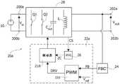
图1是DC/DC电子转换器20的示意图。尤其,通用电子转换器20包括用于接收DC电压Vin的两个输入端子200a和200b以及用于提供DC电压Vout的两个输出端子202a和202b。例如,输入电压Vin可以由诸如电池的DC电压源10提供,或者可以借助于诸如桥式整流器的整流器电路以及可能的滤波电路从AC电压获得。相反,输出电压Vout可以用于向负载30供电。FIG. 1 is a schematic diagram of a DC/DC
如公知的,电子转换器包括一个或多个电抗组件,例如电感和/或电容,以及一个或多个电子开关,电子开关被配置成控制:从输入端子200a和200b到一个或多个电抗组件的电流流动、和/或从一个或多个电抗组件到输出端子202a和202b的电流流动。As is known, an electronic converter includes one or more reactive components, such as inductors and/or capacitors, and one or more electronic switches configured to control: from the
例如,图2示出典型的电子转换器20a。具体地,电子转换器20a包括连接在输入端子200a、200b与输出端子202a、202b之间的开关级/电路28。这种开关级28包括一个或多个电抗组件,例如一个或多个电感L、例如电感器或变压器,和/或一个或多个电容器C。此外,开关级28包括一个或多个电子开关,诸如开关Q1和Q2,电子开关被配置成控制流过一个或多个电抗组件的一个或多个电流。例如,在典型的电子转换器中,一个或多个电子开关用于控制流经电感L的电流,电感L例如是电感器(例如,在升压、降压或降压-升压转换器的情况下)或变压器(例如,在反激、正向或半桥转换器的情况下)。For example, Figure 2 shows a typical
电子转换器20a通常还包括控制电路22a,控制电路被配置成驱动一个或多个电子开关的开关,以便获得所请求的输出电压Vout。The
例如,为此目的,电子转换器20a可以包括反馈(FBC)电路24,例如分压器,反馈(FBC)电路被配置成生成指示输出电压Vout(并且优选与输出电压成比例)的反馈信号FB,并且控制电路22a被配置成通过将反馈信号FB与参考信号(例如参考电压Vref)进行比较来生成用于一个或多个电子开关的驱动信号。For example, for this purpose, the
例如,如本领域所公知的,开关级28可以被配置成使得流经电感L的电流可以在连续导通模式(CCM)、不连续导通模式(DCM)或过渡模式(TM)中(经由一个或多个电子开关)被控制。For example, as is known in the art, switching
例如在CCM中,控制电路22a通常以包括两个开关阶段的开关时段来驱动开关级28的电子开关(使用驱动器电路220),其中:在第一阶段期间,流经电感L的电流增加;并且在第二阶段期间,流经电感L的电流减小。In CCM, for example, the
相反地,在DCM中,控制电路22a通常以包括三个开关阶段的开关时段来驱动开关级28的电子开关,其中:在第一阶段期间,流经电感L的电流增加;在第二阶段期间,流经电感L的电流减小,其中当流经电感L的电流达到零时,第二阶段结束;并且在第三阶段期间,流经电感L的电流保持为零。Conversely, in DCM, the
例如在DCM中,第三阶段的开始可以是转换器拓扑所固有的(例如,通过使用一个或多个二极管,当流经电感L的电流达到零时该二极管自动断开),或者如图2所示,通过使用零电流检测(ZCD)电路26,该电路被配置成通过监控指示流经电感L的电流(并且优选地与该电流成比例)的信号CS来生成零电流信号ZC。In DCM, for example, the onset of the third phase can be inherent to the converter topology (eg, by using one or more diodes that automatically turn off when the current through the inductor L reaches zero), or as shown in Figure 2 As shown, using a zero current detection (ZCD)
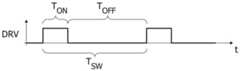
通常,大量的驱动方案在本领域中是已知的。例如,在各种已知的解决方案中,开关周期TSW的持续时间可以是恒定的,并且第一阶段的持续时间可以经由比例积分(PI)或比例积分微分(PID)调节器来确定,比例积分(PI)或比例积分微分(PID)调节器被配置成调节参考信号Vref与由反馈电路24提供的反馈信号FB之间的差。例如,这通过PWM生成器电路220示意地示出,该PWM生成器电路被配置成生成PWM信号DRV,该PWM信号具有开关周期TSW(例如,具有固定或预定的时段),其中信号DRV在第一持续时间TON内被设置为第一逻辑电平(例如,高电平),在第二持续时间TOFF内被设置为第二逻辑电平(例如,低电平),其中TSW=TON+TOFF(也参见图3)。例如,电路220可以是模拟和/或数字PI或PID调节器,其被配置成改变接通持续时间TON以便将参考信号Vref与反馈信号FB之间的差调节为零。In general, a large number of drive schemes are known in the art. For example, in various known solutions, the duration of the switching period TSW may be constant, and the duration of the first phase may be determined via a proportional-integral (PI) or proportional-integral-derivative (PID) regulator, A proportional-integral (PI) or proportional-integral-derivative (PID) regulator is configured to regulate the difference between the reference signal Vref and the feedback signal FB provided by the
因此,在所考虑的示例中,电子转换器20、20a是被配置成提供经调节的输出电压Vout的电压源。这种电压源也可以用于提供恒定电流负载。例如,图4A和图4B示出典型的情况,其中,(调节)电压源20用于向给定数量n的并联连接的发光二极管(LED)串34供电,其中每个LED串包括给定数量N的LED或类似的固态光源L,诸如激光二极管或OLED(有机发光二极管)。例如,在图4A和图4B中示出4个串,其中:第一串包括五个光源L;第二串包括四个光源L;第三串包括三个光源L;第四串包括两个光源L。Thus, in the example considered, the
例如,这种串34可以用作LCD面板的背景照明,或者通常用于其中必须单独控制流过每个串34的电流的任何应用中。
此外,如图5所示,通常也可以单独地控制流过给定串34的每个光源L的电流。例如,为此目的,每个光源L可以并联连接相应的电子开关Sw,即,用于给定串34的光源L1、...、LN的开关SW1、...、SWN,其中每个电子开关通过各自的驱动信号Sw_ctrl1、...、Sw_ctrlN来驱动。因此,通过还使用光源L的单独控制,LED串也可以用作有源LED或OLED面板。Furthermore, as shown in FIG. 5 , the current flowing through each light source L of a given
因此,在许多应用中:各个串34的固态光源的数量N可以不同;和/或一个或多个串34的接通的固态光源L的数量可以随时间变化。Thus, in many applications: the number N of solid state light sources for each
然而,这意味着在各个并联连接的LED串34处的电压降可以彼此不同和/或可以随时间变化。此外,电压降也可能由于制造公差、温度(尤其是在OLED面板的情况下)和老化而变化。为此,LED串通常不是直接经由电压源20提供的电压Vout供电,而是电流调节器/限制器32与每个LED串34串联连接。However, this means that the voltage drops at the individual parallel connected
例如,在图4A中,每个LED串34的正端子连接(例如,直接连接)到正输出端子202A,并且每个LED串34的负端子经由相应的电流调节器/限制器32(即,电流吸收器)连接(例如,直接连接)到负输出端子202b。相反,在图4B中,每个LED串34的负端子连接(例如,直接连接)到负输出端子202b,并且每个LED串34的正端子经由相应的电流调节器/限制器32(即电流源)连接(例如,直接地连接)到正输出端子202a。For example, in Figure 4A, the positive terminal of each
因此,每个电流调节器/限制器32被配置成将流过相应LED串34的电流值设置(在调节器的情况下)或限制(在电流限制器的情况下)到例如用于第一串的值I1、用于第二串的值I2、等等。例如,通常每个电流调节器/限制器32被配置成根据控制信号CTRL设置相应的电流,例如:将所述相应电流设定为零,从而关断所述相应LED串;或者将相应的电流设置为给定(固定或可以设置的)值,从而接通(激活)相应的LED串,其中由相应的LED串发射的光的亮度取决于给定值。Thus, each current regulator/
通常,如所公知的,以这种方式,通过控制由各种光源L发射的光的强度,也可以设置由LED串发射的光的颜色。In general, in this way, by controlling the intensity of the light emitted by the various light sources L, the color of the light emitted by the LED string can also be set, as is well known.
例如,为此目的,每个电流调节器/限制器32可以被配置成根据一个或多个(模拟和/或数字)控制信号(诸如用于第一电流调节器/限制器32的控制信号CTRL1、用于第二电流调节器/限制器32的控制信号CTRL2等)接通或关断相应的LED串和/或设置相应电流的值。通常,除了前面讨论的问题外,流过LED串的电流的不同值的设置通常也暗示每个发光元件L处的电压降可以随时间变化。For example, each current regulator/
例如,通过使用用于控制信号CTRL的脉宽调制(PWM)信号,由给定串34的光源发射的光的(平均)强度取决于相应PWM信号CTRL的占空比。类似地,通过使用信号Sw_ctrl1、...、Sw_ctrlN的PWM信号,由给定串34的每个光源发射的光的(平均)强度取决于相应PWM信号Sw_ctrl的占空比。For example, by using a pulse width modulated (PWM) signal for the control signal CTRL, the (average) intensity of light emitted by the light sources of a given
因此,通常电流调节器/限制器32的给定(最大)值是固定的,并且光源34的亮度经由PWM信号CTRL和/或Sw_CTRL、通过接通和关断所述串34和/或各个光源L来控制。实际上,电流调节器/限制器32被配置成设置流过每个LED串34的电流值。此外可选地,每个LED串34的各种光源也可以单独地接通或关断,由此电流可以仅流过光源的子集,即,电流调节器/限制器32被配置成设置用于相应LED串的全局电流,并且附加开关可以用于使流过该串的光源中的一个或多个光源的电流无效。Therefore, typically the given (maximum) value of the current regulator/
通常,电流调节器/限制器32是线性电流调节器,这因此意味着相应LED串处的电压Vout与电压降之间的差被施加到电流调节器/限制器32,这基本耗散了过量的功率,从而生成电损耗。Typically, the current regulator/
为此,通常优选地将电压Vout维持在略高于LED串处的最大电压降。因此,在电压Vout固定的情况下,电压Vout必须等于(或大于)需要最大供电电压的最坏情况。相反,自适应系统也是例如从美国专利申请公开号2004/0233144或2010/0156315或美国专利号6,864,641已知的,所有这些美国专利申请公开都通过引用并入本文,其中,输出电压Vout的值根据LED串34或电流调节器/限制器32处的电压降而变化。For this reason, it is generally preferable to maintain the voltage Vout slightly above the maximum voltage drop at the LED string. Therefore, with the voltage Vout fixed, the voltage Vout must be equal to (or greater than) the worst case where the maximum supply voltage is required. In contrast, adaptive systems are also known, for example, from US Patent Application Publication Nos. 2004/0233144 or 2010/0156315 or US Patent No. 6,864,641, all of which are incorporated herein by reference, wherein the value of the output voltage Vout Varies according to the voltage drop at the
这种解决方案通常包括校准阶段,其中确定LED串34处的最大电压降。例如为此目的,通过一次一个地接通LED串或者同时接通所有LED串,LED面板的操作功能被校准过程本身周期性地中断。Such solutions typically include a calibration phase in which the maximum voltage drop at the
然而,在LED用于发信号通知危险情况的情形下,例如在汽车行业中,例如在尾灯的情况下,这些方法代表了LED系统的显著限制,该尾灯应当能够发信号通知突然制动或方向指示器。此外例如,在有源LED面板的情况下,每串的激活光源的数量可能频繁变化,由此最坏情况的假设仍然生成显著的功率损耗。However, in situations where LEDs are used to signal dangerous situations, such as in the automotive industry, for example in the case of taillights, these approaches represent a significant limitation of LED systems, which should be able to signal sudden braking or direction indicator. Also, for example, in the case of active LED panels, the number of activated light sources per string may vary frequently, whereby worst-case assumptions still generate significant power losses.
鉴于上述情况,在本领域中需要提供用于基于实际负载需求来动态地适配电压源的输出电压的解决方案。In view of the above, there is a need in the art to provide a solution for dynamically adapting the output voltage of a voltage source based on actual load demands.
发明内容SUMMARY OF THE INVENTION
根据一个或多个实施例,提供了一种电流供应系统。实施例还涉及相关的集成电路、电源系统和操作电流供应系统的方法。According to one or more embodiments, a current supply system is provided. Embodiments also relate to related integrated circuits, power supply systems, and methods of operating current supply systems.
本公开的各种实施例涉及例如在集成电路中实现的电流供应系统。Various embodiments of the present disclosure relate to current supply systems implemented, for example, in integrated circuits.
具体地,在各种实施例中,电流供应系统包括被配置成连接到电压源的第一输出端子上的一个或多个第一端子以及多个第二端子,其中,第二端子中的每个第二端子被配置成经由相应固态光源串连接到电压源的第二输出端子。Specifically, in various embodiments, the current supply system includes one or more first terminals and a plurality of second terminals configured to be connected to a first output terminal of a voltage source, wherein each of the second terminals The second terminals are configured to be connected to the second output terminals of the voltage source via the respective strings of solid state light sources.
在各种实施例中,电流供应系统包括多个电流调节器或限制器,其中,第二端子中的每个第二端子经由相应的电流调节器或限制器连接到一个或多个第一端子中的至少一个第一端子,其中,所述电流调节器或限制器中的每个电流调节器或限制器被配置成将流经连接到相应第二端子的固态光源串的电流限制到相应最大值。因此,电流供应系统可以用于限制也包括电压源和可选地固态光源串的电源系统中的电流流动。In various embodiments, the current supply system includes a plurality of current regulators or limiters, wherein each of the second terminals is connected to one or more of the first terminals via a respective current regulator or limiter at least one first terminal in, wherein each of the current regulators or limiters is configured to limit the current flowing through the string of solid state light sources connected to the corresponding second terminal to a corresponding maximum value. Thus, the current supply system can be used to limit current flow in a power supply system that also includes a voltage source and optionally a string of solid state light sources.
在各种实施例中,电流供应系统还包括第三端子,第三端子被配置成向电压源提供参考信号,其中,参考信号指示将由电压源在电压源的第一输出端子和第二输出端子之间生成的所请求的输出电压。因此,控制电路可以被配置成生成该参考信号。In various embodiments, the current supply system further includes a third terminal configured to provide a reference signal to the voltage source, wherein the reference signal indicates that the voltage source is to be supplied by the voltage source at the first output terminal and the second output terminal of the voltage source generated between the requested output voltages. Accordingly, the control circuit may be configured to generate the reference signal.
具体地,在各种实施例中,控制电路包括至少一个模数转换器和数模转换器转换电路。具体地,至少一个模数转换器被配置成获得第二端子处的电压和电压源的第一输出端子与第二输出端子之间的电压(即,由电压源生成的输出电压)的数字样本。数模转换器转换电路被配置成接收数字调节值并且在输出处向第三端子/电压源提供参考信号。Specifically, in various embodiments, the control circuit includes at least one analog-to-digital converter and a digital-to-analog converter conversion circuit. Specifically, the at least one analog-to-digital converter is configured to obtain digital samples of the voltage at the second terminal and the voltage between the first and second output terminals of the voltage source (ie, the output voltage generated by the voltage source). . The digital-to-analog converter conversion circuit is configured to receive the digital adjustment value and provide a reference signal at the output to the third terminal/voltage source.
例如,通常参考信号可以用于设置电压源的参考电压,例如,参考信号可以与将由电压源生成的所请求的输出电压成比例。在这种情况下,数模转换器转换电路可以包括模数转换器,模数转换器被配置成根据数字调节值直接生成参考信号。然而,参考信号也可以用于改变电压源的反馈信号。例如,在这种情况下,第三端子可以耦联到电压源的反馈端子,以便改变指示由电压源生成的输出电压的反馈信号。For example, typically a reference signal may be used to set the reference voltage of the voltage source, eg, the reference signal may be proportional to the requested output voltage to be generated by the voltage source. In this case, the digital-to-analog converter conversion circuit may comprise an analog-to-digital converter configured to generate the reference signal directly from the digital adjustment value. However, the reference signal can also be used to vary the feedback signal of the voltage source. For example, in this case, the third terminal may be coupled to the feedback terminal of the voltage source in order to vary the feedback signal indicative of the output voltage generated by the voltage source.
在各种实施例中,控制电路包括数字前馈控制电路和数字反馈控制电路两者。In various embodiments, the control circuit includes both a digital feedforward control circuit and a digital feedback control circuit.
在各种实施例中,前馈控制电路被配置成通过根据数字样本确定第二端子与电压源的第二输出端子之间(即,在固态光源的串处)的最大电压降并且通过将给定的裕量加到该最大电压降来计算指示所请求的输出电压的数字前馈调节值。In various embodiments, the feedforward control circuit is configured by determining the maximum voltage drop between the second terminal and the second output terminal of the voltage source (ie, at the string of solid state light sources) from the digital samples and by giving the A certain margin is added to this maximum voltage drop to calculate a digital feedforward regulation value indicative of the requested output voltage.
相反,在各种实施例中,反馈控制电路被配置成根据数字样本确定多个电流调节器或限制器处的最小电压降并且根据最小电压降和裕量之间的差确定反馈校正值。Rather, in various embodiments, the feedback control circuit is configured to determine the minimum voltage drop at the plurality of current regulators or limiters from the digital samples and to determine the feedback correction value from the difference between the minimum voltage drop and the headroom.
在各种实施例中,控制电路被配置成响应于电流供应系统的启动,将数字调节值设置成指示所请求的最大输出电压的第一值,即,最初电压源提供最大供电电压。In various embodiments, the control circuit is configured to, in response to activation of the current supply system, set the digital adjustment value to a first value indicative of the requested maximum output voltage, ie, initially the voltage source provides the maximum supply voltage.
在各种实施例中,控制电路然后被配置成确定数字调节值是否对应于第一(最大)值。在这种情况下,控制电路根据前馈值设置数字调节值,例如,将数字调节值设置为前馈值,由此电压源从最大值“跳”到与前馈值相对应的新的输出电压。相反地,当数字调节值不对应于第一值时(例如,因为已经使用了前馈值),控制电路可以将反馈校正值加到数字调节值,从而实现输出电压的微调。In various embodiments, the control circuit is then configured to determine whether the digital adjustment value corresponds to the first (maximum) value. In this case, the control circuit sets the digital adjustment value according to the feedforward value, e.g. the digital adjustment value is set to the feedforward value, whereby the voltage source "jumps" from the maximum value to a new output corresponding to the feedforward value Voltage. Conversely, when the digital adjustment value does not correspond to the first value (eg, because a feedforward value has been used), the control circuit may add a feedback correction value to the digital adjustment value, thereby enabling fine adjustment of the output voltage.
通常,控制电路也可以检测各种事件并且将数字调节值设置为最大值(从而重新激活前馈控制)或者最小值(从而使对固态光源串的电流供应无效)。Typically, the control circuit can also detect various events and set the digital adjustment value to a maximum value (thus reactivating the feedforward control) or a minimum value (thus deactivating the current supply to the solid state light source string).
例如,在各种实施例中,电流调节器或限制器中的每个被配置成从控制电路接收指示至少第一操作模式和第二操作模式的至少一个控制信号。例如,当至少一个控制信号指示第一操作模式时,相应的电流调节器或限制器可以被配置成使所述电流无效。相反,当所述至少一个控制信号指示第二操作模式时,相应的电流调节器或限制器可以被配置成将电流限制到相应的最大值。例如为此目的,所述至少一个控制信号可以包括脉宽调制信号,其中,脉宽调制信号的第一逻辑电平指示第一操作模式,并且脉宽调制信号的第二逻辑电平指示第二操作模式。通常,至少一个控制信号也可以指示最大值。例如,这样的控制信号可以用于选择性地接通或关断所述串和/或执行对由光源发射的光进行调光。For example, in various embodiments, each of the current regulator or limiter is configured to receive at least one control signal from the control circuit indicative of at least a first mode of operation and a second mode of operation. For example, when at least one control signal indicates a first mode of operation, a corresponding current regulator or limiter may be configured to disable the current. Conversely, when the at least one control signal indicates the second mode of operation, the corresponding current regulator or limiter may be configured to limit the current to the corresponding maximum value. For example for this purpose, the at least one control signal may comprise a pulse width modulation signal, wherein a first logic level of the pulse width modulation signal indicates a first mode of operation and a second logic level of the pulse width modulation signal indicates a second operating mode. Typically, at least one control signal may also indicate a maximum value. For example, such a control signal may be used to selectively turn the strings on or off and/or perform dimming of the light emitted by the light source.
例如,在这种情况下,控制电路可以被配置成根据控制信号确定是否应当关断所有固态光源串。例如,在PWM信号的情况下,控制电路可以确定控制信号是否指示所有电流调节器或限制器对于完整的PWM周期或对于多个PWM周期被关断(第一操作模式)。在这种情况下,控制电路也可以通过将数字调节值设置成指示所请求的最小输出电压的第二值来(基本)使所述电压源无效。For example, in this case, the control circuit may be configured to determine from the control signal whether all strings of solid state light sources should be turned off. For example, in the case of a PWM signal, the control circuit may determine whether the control signal instructs all current regulators or limiters to be turned off for a full PWM cycle or for multiple PWM cycles (first mode of operation). In this case, the control circuit may also (substantially) deactivate the voltage source by setting the digital adjustment value to a second value indicative of the requested minimum output voltage.
另外,控制电路可以被配置成根据控制信号确定是否应当接通固态光源串中的至少一个固态光源串(第二操作模式)。例如,在PWM信号的情况下,控制电路可以确定控制信号是否指示至少一个电流调节器或限制器应当在当前PWM周期期间被接通。Additionally, the control circuit may be configured to determine from the control signal whether at least one of the strings of solid state light sources should be turned on (second mode of operation). For example, in the case of a PWM signal, the control circuit may determine whether the control signal indicates that at least one current regulator or limiter should be turned on during the current PWM cycle.
具体地,在使输出电压无效的情况下,控制电路可以通过开始新的前馈控制动作来恢复操作。具体地,响应于已经确定至少一个电流调节器或限制器应当被接通,控制电路可以验证数字调节值是否对应于第二(最小)值(指示输出电压具有其最小值)。在这种情况下,控制电路可以将数字调节值设置成第一(最大)值。因此,响应于将数字调节值设置成第一(最大)值,电压源将提供最大输出电压,并且控制电路将再次根据前馈值(在给定时段之后)设置数字调节值。Specifically, in the event of deactivating the output voltage, the control circuit can resume operation by starting a new feedforward control action. Specifically, in response to having determined that at least one current regulator or limiter should be turned on, the control circuit may verify whether the digital regulation value corresponds to the second (minimum) value (indicating that the output voltage has its minimum value). In this case, the control circuit may set the digital adjustment value to the first (maximum) value. Thus, in response to setting the digital adjustment value to the first (maximum) value, the voltage source will provide the maximum output voltage and the control circuit will again set the digital adjustment value according to the feedforward value (after a given period).
在各种实施例中,控制电路也可以确定光源是否确实被供电。例如,为此目的,控制电路可以确定控制信号是否指示至少一个电流调节器或限制器应当使用第二操作模式。在这种情况下,控制电路可以确定电流是否流过应当使用第二操作模式的至少一个电流调节器或限制器。例如,响应于确定没有电流流过应当使用第二操作模式的电流调节器或限制器中的至少一个,控制电路可以改变数字调节值以便增加所请求的输出电压。In various embodiments, the control circuit may also determine whether the light source is indeed powered. For example, for this purpose, the control circuit may determine whether the control signal indicates that the at least one current regulator or limiter should use the second mode of operation. In this case, the control circuit may determine whether current is flowing through the at least one current regulator or limiter that should use the second mode of operation. For example, in response to determining that no current is flowing through at least one of the current regulator or limiter that should use the second mode of operation, the control circuit may change the digital regulation value to increase the requested output voltage.
附图说明Description of drawings
现在将参考附图描述本公开的实施例,附图仅通过非限制性示例的方式提供,并且其中:Embodiments of the present disclosure will now be described with reference to the accompanying drawings, provided by way of non-limiting example only, and in which:
图1示出典型的电源系统;Figure 1 shows a typical power system;
图2和图3示出利用电子转换器实现的电压源的示例;Figures 2 and 3 show examples of voltage sources implemented with electronic converters;
图4A、图4B和图5示出电源系统的示例,其中,电压源和电流供应系统用于向多个固态光源串供电;Figures 4A, 4B and 5 illustrate examples of power supply systems in which a voltage source and current supply system are used to power multiple strings of solid state light sources;
图6和图7示出用于固态光源串的电流供应系统的实施例;6 and 7 illustrate embodiments of current supply systems for strings of solid state light sources;
图8和图9示出用于图6和图7的电流供应系统的控制电路的实施例;Figures 8 and 9 illustrate embodiments of control circuits for the current supply system of Figures 6 and 7;
图10和图11示出图8和图9的控制电路的操作的实施例;Figures 10 and 11 illustrate an embodiment of the operation of the control circuit of Figures 8 and 9;
图12和图13示出实施例,其中,多个电流供应系统连接至同一电压源;以及Figures 12 and 13 illustrate embodiments in which multiple current supply systems are connected to the same voltage source; and
图14示出用于固态光源串的电流供应系统的另外的实施例。Figure 14 shows a further embodiment of a current supply system for a string of solid state light sources.
具体实施方式Detailed ways
在以下描述中,给出了许多具体细节以提供对实施例的透彻理解。可以在没有一个或几个具体细节的情况下,或者利用其他方法、组件、材料等来实施所述实施例。在其他情况下,没有详细示出或描述公知的结构、材料或操作,以避免使实施例的方面模糊。In the following description, numerous specific details are set forth to provide a thorough understanding of the embodiments. The described embodiments may be practiced without one or more of the specific details, or with other methods, components, materials, etc. In other instances, well-known structures, materials, or operations have not been shown or described in detail to avoid obscuring aspects of the embodiments.
在整个说明书中对“一个实施例”或“实施例”的引用意味着结合该实施例描述的特定特征、结构或特性被包括在至少一个实施例中。因此,在本说明书中的各个地方出现的短语“在一个实施例中”或“在实施例中”不一定全部指代同一实施例。此外,特定特征、结构或特性可以以任何合适的方式组合在一个或多个实施例中。Reference throughout this specification to "one embodiment" or "an embodiment" means that a particular feature, structure or characteristic described in connection with the embodiment is included in at least one embodiment. Thus, appearances of the phrases "in one embodiment" or "in an embodiment" in various places in this specification are not necessarily all referring to the same embodiment. Furthermore, the particular features, structures or characteristics may be combined in any suitable manner in one or more embodiments.
本文提供的标题仅为了方便起见并且不解释实施例的范围或含义。The headings provided herein are for convenience only and do not interpret the scope or meaning of the embodiments.
在下面的图6至图14中,将注意到,已经参考图1和图5描述的部件、元件或组件由先前在这些图中使用的相同附图标记表示;为了不使本具体实施方式过于复杂,下面将不再重复对这些前述元件的描述。In Figures 6 to 14 below, it will be noted that parts, elements or assemblies that have been described with reference to Figures 1 and 5 are designated by the same reference numerals previously used in these Figures; in order not to obscure the present detailed description Complicated, the description of these aforementioned elements will not be repeated below.
如前所述,本说明书涉及用于向负载供应电流的解决方案,所述负载诸如是如关于图4A、图4B或图5所描述的固态光源L的串34。As previously mentioned, the present specification relates to a solution for supplying current to a load, such as a
图6示出与图4B的描述一致的第一实施例,并且图7示出与图4B的描述一致的第一实施例。FIG. 6 shows a first embodiment consistent with the description of FIG. 4B , and FIG. 7 shows a first embodiment consistent with the description of FIG. 4B .
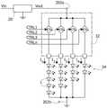
具体地,图6和图7示出用于固态光源L的多个串34(诸如LED串或OLED串)的电源系统的实施例。In particular, FIGS. 6 and 7 illustrate an embodiment of a power supply system for
具体地,在所考虑的实施例中,电源系统包括可变电压源20,所述可变电压源包括:两个输入端子(例如,关于图1和图2描述的端子200a和200b)被配置成接收输入电压Vin,并且正输出端子202a和负输出端子202b被配置成提供(调节的)输出电压Vout。Specifically, in the embodiment under consideration, the power supply system includes a
通常,电压源20可以是线性调节器,或者优选地是如关于图2和图3所描述的开关模式电子转换器。例如,在图6和图7中示意地示出电压源20,该电压源被配置成接收:来自反馈电路24(例如包括至少两个电阻器R1和R2的分压器)的指示输出电压Vout(并且优选地与输出电压成比例)的反馈信号FB;以及指示所请求的输出电压Vout(并且优选与所请求的输出电压成比例)的参考信号Vref。Typically, the
在各种实施例中,反馈电路24也可以直接集成在电压源20中。In various embodiments, the
在所考虑的实施例中,电源系统还包括电流供应系统。具体地,电流供应系统包括:In the considered embodiment, the power supply system further comprises a current supply system. Specifically, the current supply system includes:
一个或多个第一端子,被配置成连接到电压源20的第一输出端子,例如,图6中的负输出端子202b或图7中的正输出端子202a;以及one or more first terminals configured to be connected to a first output terminal of the
给定数量n的第二端子OUT1、...、OUTn(例如端子OUT1、...、OUT4),其中,每个第二端子OUT被配置成经由相应的固态光源串34连接到电压源20的第二输出端子,例如图6中的正输出端子202a或图7中的负输出端子202b;以及A given number n of second terminals OUT1 , . . . , OUTn (eg, terminals OUT1 , . the second output terminal of , such as the
给定数量N的电流调节器/限制器32,其中,相应的电流调节器/限制器32(例如直接)连接在相应的第二端子OUT和所述一个或多个第一端子中的至少一个第一端子之间。a given number N of current regulators/
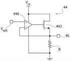
具体而言,每个电流调节器/限制器32被配置成将流经电流调节器/限制器32的电流根据相应控制信号CTRL(即信号CTRL1、...、CTRL)限制成相应的最大值,由此每个电流调节器/限制器32被配置成将流经相应固态光源串34的电流限制成相应的最大值。具体地,电流调节器/限制器32在图6中所示的实施例中是电流吸收器,并且在图7中所示的实施例中是电流源。Specifically, each current regulator/
在所考虑的实施例中,电流供应系统还包括用于向电压源20提供参考信号Vref的另外的端子和控制电路40,控制电路被配置成:生成控制信号CTRL1、...、CTRLn;监控第二端子OUT1、...、OUTn中的每个第二端子处的电压;并且在所述另外的端子处生成参考信号Vref,从而设置所请求的输出电压Vout。In the considered embodiment, the current supply system further comprises further terminals for supplying the reference signalVref to the
在各种实施例中,电流供应系统、尤其是电流调节器/限制器32和控制电路40可以在同一集成电路中实现。在各种实施例中,电压源20的控制电路22(参见图2)也可以实现在同一集成电路中。In various embodiments, the current supply system, particularly the current regulator/
如前所述,在各种实施例中,控制信号CTRL可以是二进制信号,其中,每个电流调节器/限制器32被配置成当信号CTRL具有第一逻辑值时将流经相应串34的电流限制为零,并且当信号CTRL具有第二逻辑值时将流经相应串的电流限制为相应(恒定)最大值。然而,信号CTRL也可以是能够直接设置最大值的模拟信号或者能够设置多个最大值的数字信号。As previously mentioned, in various embodiments, the control signal CTRL may be a binary signal, wherein each current regulator/
例如,在各种实施例中,控制电路40被配置成生成作为脉宽调制(PWM)信号的信号CTRL,其中,信号具有相同的开关时段,但是每个信号CTRL具有各自的占空比。For example, in various embodiments, the
在各种实施例中,串34还可以包括不同数量的光源L(参见图4A和图4B的描述)。附加地或替代地,每个光源L也可以具有相关联的相应电子开关,该电子开关被配置成选择性地使光源L短路,从而允许对每个光源的电源的单独控制(参见图5的描述)。In various embodiments,
因此,每个信号CTRL也可以包括多个模拟信号和/或数字信号,例如用于设置最大值的信号,以及一个或多个PWM信号,用于接通和关断相应的LED串34和/或光源L的或相应的LED串34的子集。Thus, each signal CTRL may also include a plurality of analog and/or digital signals, such as a signal for setting a maximum value, and one or more PWM signals for switching on and off the corresponding
例如在各种实施例中,控制电路40可以被配置成生成信号CTRL和可选地生成用于附加电子开关Sw的驱动信号Sw_CTRL,以便生成例如有源LED或OLED面板的所请求的照明模式。例如,为此目的,控制电路40可以包括用于接收识别所请求的照明模式的数据的通信接口。For example, in various embodiments, the
因此,在各种实施例中,固态光源的被激活的串34的数量可以随时间而改变。此外,在各种实施例中,串34的固态光源的数量可以不同(基于应用),或者被激活的串34的被激活的固态光源的数量可以随着时间而改变,即,被激活的串34处的电压降可以随着时间而改变。此外,在被激活的串34处的电压降也可能由于其他原因(诸如温度变化)和/或由于流过该串的最大电流的不同设置而改变。Thus, in various embodiments, the number of activated
在各种实施例中,控制电路40被配置成根据端子OUT1、...、OUTn处的电压VOUT1、...、VOUTn生成参考信号Vref。通常,控制电路40可以被配置成测量端子OUT1、...、OUTn处的相对于正端子202a(即Vout)或优选地相对于负端子202b(即接地)的电压VOUT1、...、VOUTn。例如,在图6中,控制电路40被配置成测量端子OUT处的相对于一个或多个第一端子(连接到负端子/接地202b)的电压,从而测量相应电流调节器/限制器32处的电压降。相反地,在图7中,控制电路40被配置成测量端子OUT处的相对于负端子/接地202b的电压,从而测量相应固态光源串34处的电压降。In various embodiments, the
具体地,在各种实施例中,控制电路40被配置成确定串34处的最大电压降VLED_MAX,并且将输出电压Vout(经由参考信号Vref)设置成大于给定量VM的值。在各种实施例中,在不中断由串34投射的当前照明模式的情况下执行该动态自适应。例如,这在汽车领域中特别有意义,其中,串34可以用于发信号通知警告情况或危险情况。在各种实施例中,动态自适应还能够调节输出电压,以便使输出电压适应于与OLED、工艺扩展和/或温度特别相关的其他变化,诸如老化现象。Specifically, in various embodiments, the
在各种实施例中,经由控制电路40内的数字处理来执行以上操作。例如,这具有的优点是,控制电路40也可以执行一系列进一步的诊断和功能操作,诸如:In various embodiments, the above operations are performed via digital processing within
-监控负载条件,例如以便确定临时或永久的开路负载或短路条件,这些负载条件例如可以用于禁用相应的光源串;- monitoring load conditions, eg in order to determine temporary or permanent open-circuit load or short-circuit conditions, which load conditions can eg be used to disable the corresponding light source string;
-监控电流调节器/限制器32和/或串34的一个或多个温度,所述一个或多个温度可以用于禁用相应的电流调节器32和串34,或者减小相应的最大电流;- monitoring one or more temperatures of the current regulator/
-实现热降额模型,其中,基于对光源的过高温度的测量来适应最大电流。- Implementing a thermal derating model, wherein the maximum current is adapted based on the measurement of excessive temperature of the light source.
如上所述,通常电流供应系统包括给定数量n的电流调节器/限制器32,所述电流调节器/限制器连接到相应端子OUT1、...、OUTn,其中每个端子OUT1、...、OUTn可以经由相应的固态光源串34连接到电压源20的输出端子。通常,实际连接到n个电流调节器/限制器32的串32的数量也可小于n。此外,每个电流调节器/限制器32可以总是被使能,或优选地经由相应的控制信号CTRL1、...、CTRLn选择性地使能,即,有源串34的数量可以是固定的或可变的。As mentioned above, typically the current supply system comprises a given number n of current regulators/
在各种实施例中,控制电路40被配置成:例如,根据该控制信号CTRL1、...、CTRLn来确定该固态光源的被激活的串34;并且确定指示在固态光源的被激活的串34处的最大电压降(并且优选地与该最大电压降成比例)的数字样本。In various embodiments, the
如前所述,控制电路40可以被配置成直接监控固态光源串34处的电压降。在这方面,最大电压降的选择可以在模拟电平(即,在模数转换之前)或在数字电平(即,在模数转换之后)执行。As previously discussed, the
可替代地,控制电路40可以被配置成监控电流调节器/限制器32处的电压降。在这种情况下,控制电路40可以根据电流调节器/限制器32处的电压降和电压Vout计算固态光源串34处的电压降。同样在这种情况下,可以在模拟电平(即,在模数转换之前)执行一个或多个先前操作,或者可以在数字电平(即,在模数转换之后)执行所有操作。Alternatively, the
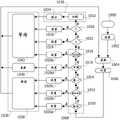
例如,图8示出控制电路40的实施例,其中控制电路40被配置成例如通过在图6中测量端子OUT处相对于端子202b/接地的电压来监控指示电流调节器/限制器32处的电压降(并且优选地与该电压降成比例)的电压。For example, FIG. 8 shows an embodiment of a
例如,在所考虑的实施例中,控制电路40被配置成获取端子OUT1、...、OUTn处的电压VOUT1、...、VOUTn的数字样本VOUT1_ADC、...、VOUTn_ADC,并且将这些数字样本VOUT1_ADC、...、VOUTn_ADC存储到存储器406。例如,如图8示意所示,为此目的,控制电路可以包括至少一个模数转换器(ADC)404以及被配置成将一个或多个模数转换器404连接到端子OUT1、...、OUTn的可选的多路复用器402。通常,多路复用器402完全是可选的,因为控制电路50也可以包括n个ADC404,即每个端子OUT1、...、OUTn一个ADC。例如,在各种实施例中,(一个或多个)ADC404具有8、12或16比特的分辨率。For example, in the embodiment under consideration, the
通常,(一个或多个)ADC的数量和相应的转换速度应当被选择以便确保可以以足够高的频率对电压VOUT1、...、VOUTn进行采样。In general, the number of ADC(s) and the corresponding conversion speed should be chosen to ensure that the voltages VOUT1 , . . . , VOUTn can be sampled at a sufficiently high frequency.
例如,如前所述,信号CTRL可以是PWM信号,其中,每个信号CTRL1、...、CTRLn对于给定的接通期间(相应的串被激活)被设置成高电平,并且对于给定的关断持续时间(相应的串被解除激活)被设置成低电平。通常,信号CTRL1、...、CTRLn也可以在完整的PWM周期期间保持低电平,由此解除激活相应的串,即,占空比可以在[0;1]的范围中被选择。For example, as before, the signal CTRL may be a PWM signal, wherein each signal CTRL1, . . . , CTRLn is set high for a given on-period (the corresponding string is activated), and is set low for a given off-time duration (the corresponding string is deactivated). Typically, the signals CTRL1, . . . , CTRLn can also remain low during a complete PWM cycle, thereby deactivating the corresponding string, ie the duty cycle can be selected in the range [0;1].
因此,该控制电路40可以被配置成获得各电压VOUT1、...、VOUTn的一个或多个数字样本,而相应的信号CTRL1、...、CTRLn被设置成高电平。例如,通常这种PWM信号具有200和1400Hz之间的频率。因此,如果PWM信号的最小接通时间大于ADC转换时间加上用于对所有信道进行采样的多路复用时间,则可以使用单个ADC 404。Thus, the
在不同的实施例中,该控制电路40也可以在不同的信号CTRL1、...、CTRL之间引入相位偏移,相位偏移允许取样不同的电压序列。在各种实施例中,该控制电路也可以被配置成:对于在给定PWM周期期间待被激活的串34,确保接通时间大于允许经由(一个或多个)ADC 404进行采样的给定最小值。In different embodiments, the
因此,在所考虑的实施例中,样本VOUT1_ADC、...、VOUTn_ADC指示电流调节器/限制器32处的电压降。Thus, in the considered embodiment, the samples VOUT1_ADC , . . . , VOUTn_ADC are indicative of the voltage drop at the current regulator/
在所考虑的实施例中,控制电路40因此也被配置成(经由一个或多个ADC 404和可选的多路复用器402)获取端子202a处的电压Vout的数字样本Vout_ADC,并且将样本Vout_ADC存储到存储器406。In the embodiment under consideration, the
具体地,在各种实施例中,控制电路40被配置成根据数字样本VOUT1_ADC、…、VOUTn_ADC及该数字样本Vout_ADC确定被激活的串32(例如,在该当前PWM周期期间相应的信号CTRL1、…、CTRLn已被设置成高电平的串34)处的最大电压降VLED_MAX。Specifically, in various embodiments, the
例如,在所考虑的实施例中,控制电路40首先在模块/电路408处选择数字样本VOUT1_ADC、…、VOUTn_ADC的最小值VOUT_MIN、即电流调节器/限制器32处的最小电压降,并且然后在模块/电路410处根据以下公式计算最大电压降VLED_MAX:For example, in the embodiment under consideration,
VLED_MAX=Vout_ADC-VOUT_MIN。 (1)VLED_MAX =Vout_ADC -VOUT_MIN . (1)
相反,图9示出实施例,其中,控制电路40被配置成例如通过在图7中测量端子OUT1、…、OUTn处相对于端子202b/接地的电压来直接监控指示串24处的电压降(并且优选地与该电压降成比例)的电压。In contrast, FIG. 9 shows an embodiment in which the
因此,在这种情况下,存储到存储器404的样本VOUT1_ADC、…、VOUTn_ADC已经指示串34处的电压降,并且控制电路40被配置成通过在块/电路416处选择数字样本VOUT1_ADC、…、VOUTn_ADC的最大值来确定最大电压降VLED_MAX。Thus, in this case, the samples VOUT1_ADC , . . . , VOUTn_ADC stored to
通常,如前所述,在块408或块416的选择应当仅使用与激活的电流调节器/限制器34相关联的样本VOUT1_ADC、…、VOUTn_ADC。这可以在AD转换期间已经实现(即,通过仅对激活的电流调节器/限制器的值进行采样)和/或通过在块408或416处根据控制信号CTRL选择样本的子集来实现。Typically, the selection at
因此,在图8和图9所示的实施例中,控制电路40被配置成获得端子OUT1、...、OUTn处的电压的数字样本,并且确定串34处的最大电压降VLED_MAX。如前所述,这也可以包括测量输出电压Vout,如图8所示。Thus, in the embodiment shown in FIGS. 8 and 9 , the
一旦获得最大电压降VLED_MAX,控制电路就可以通过将给定的裕量电压VM加到最大电压降VLED_MAX来确定所请求的输出电压Vout_req,即:Once the maximum voltage dropVLED_MAX is obtained, the control circuit can determine the requested output voltageVout_req by adding the given headroom voltageVM to the maximum voltage dropVLED_MAX , namely:
Vout_req=VLED_MAX+VM。 (2)Vout_req =VLED_MAX+ VM . (2)
例如,对于典型的电流调节器/限制器,0.5V至1.5V的裕量电压,例如在0.5V和1.0V之间,是足够的。For example, for a typical current regulator/limiter, a headroom voltage of 0.5V to 1.5V, eg between 0.5V and 1.0V, is sufficient.
例如,图8和图9示意地示出加法器块/电路412,加法器块/电路被配置成通过将数字值VM加到数字值VLED_MAX来生成数字信号Vout_req。For example, FIGS. 8 and 9 schematically illustrate an adder block/
此外,控制电路40被配置成根据所请求的输出电压Vout_req确定参考信号Vref的值。具体地,如前所述,在各个实施例中,反馈信号FB与输出电压成比例,并且电压源20被配置成将反馈信号FB调节为参考信号Vref,即,输出电压可以计算如下:Furthermore, the

例如,通过使用如图6和图7所示的分压器,输出电压可以计算如下:For example, by using the voltage divider shown in Figure 6 and Figure 7, the output voltage can be calculated as follows:

因此,通过重新表述公式(2)和(3),参考信号Vref的值可以计算为:Therefore, by restating equations (2) and (3), the value of the reference signalVref can be calculated as:
Vref=K·(VLED_MAX+VM)。 (5)Vref =K·(VLED_MAX+ VM ). (5)
例如,在各种实施例中,比例值K可以在控制电路40中固定,并且反馈电路24应当被配置成使用相同的比例值K。可替代地,值K可以是可编程的。For example, in various embodiments, the scale value K may be fixed in the
例如,图8和图9示出数模转换器(DAC)418以及块/电路414,数模转换器被配置成根据数字信号Vreg生成参考信号Vref,块/电路被配置成例如通过根据系数缩放信号Vout_req来根据数字信号Vout_req生成Vreg。实际上,电路414可以被配置成使用比例值,该比例值还考虑了DAC 418的转换率,以便获得如公式(5)所示的所请求的参考信号Vref。For example, FIGS. 8 and 9 show a digital-to-analog converter (DAC) 418 configured to generate a reference signalVref from a digital signalVreg and a block/
因此,在各种实施例中,输出电压Vout被设置成在给定PWM周期期间被激活的所述串34处的最大电压降VLED_MAX加上附加的裕量电压VM,从而在所有操作条件下自动优化所供应的功率。Thus, in various embodiments, the output voltageVout is set to the maximum voltage dropVLED_MAX at the
然而,在下一个PWM时段期间激活附加串34的情况下,该串34可以具有大于或小于先前最大电压降的电压降。例如,在电压降较大的情况下,输出电压Vout可能太小而不能为该串34的光源供电,由此相应的光源不被接通,从而导致开路负载条件。However, where an
在各种实施例中,控制电路40被配置成例如基于相应的电压VOUT1_ADC、...、VOUTn_ADC的值或通过使用附加的电流传感器来确定这样的开路负载条件,并且然后将值Vref设置为给定的最大值Vref_MAX。In various embodiments, the
附加地或可替代地,控制电路40可以被配置成:当激活串34时,存储相应的值VOUT1_ADC、...、VOUTn_ADC;当串34是被解除激活的串34时,保持存储的相应值VOUT1_ADC、...、VOUTn_ADC;并且一旦在随后的PWM周期期间激活新的串34,则使用存储的值以便确定存储的值是否大于先前的最大值VLED_MAX;并且在存储的值更大的情况下,将值Vref设置为给定的最大值Vref_MAX。Additionally or alternatively, the
因此,在具有超过先前计算的最大值VLED_MAX的电压降的串34被使能的情况下,控制电路40可以立即将输出DAC 414的值设置为最大值。Thus, in the event that a
因此,在迄今为止所考虑的实施例中,使用了参考信号Vref的开环/前馈控制。实际上,系数K的值是固定的,或者例如在块414中设置在控制电路40内,而反馈电路应当被配置成例如经由比率R1/R2使用相同的系数K。因此,在串34处的最大电压降VLED_MAX显著变化的情况下,这种类型的控制尤其有用。Therefore, in the embodiments considered so far, open loop/feedforward control of the reference signalVref is used. In practice, the value of the coefficient K is fixed or set within the
然而,由于组件的扩展或温度变化而引起的常数K和反馈电路24的相应反馈比(例如,比率R1/R2)的微弱变化可能使调节电压Vout达到比预期更高或更低的值,结果是在电流调节器/限制器32处的应当对应于电压VM的最小电压降V32_MIN增加或减小,从而在一种情况下在增加的功率消耗方面或者在另外的情况下不允许正确的电流供应方面影响系统的优化。However, slight changes in the constant K and the corresponding feedback ratio of the feedback circuit 24 (eg, the ratio R1/R2) due to component expansion or temperature changes may cause the regulation voltageVout to reach a higher or lower value than expected, The result is an increase or decrease in the minimum voltage drop V32_MIN at the current regulator/
因此,在各种实施例中,当系统接通时(例如,通过暂时接通所有串34),并且可选地当在随后的PWM周期期间一个或多个串34不再被激活时和/或当在随后的PWM周期期间一个或多个附加串34被重新激活时,使用先前的前馈控制来设置参考信号Vref。通常,如将在下面更详细地描述的,前馈控制也可以响应于检测到其他事件而被使用。Thus, in various embodiments, when the system is turned on (eg, by temporarily turning on all strings 34), and optionally when one or
相反,附加的闭环控制被用于调节参考信号Vref,以便将电流调节器/限制器32处的最小电压降V32_MIN调节到值VM(也参见公式(5))。Instead, additional closed-loop control is used to adjust the reference signalVref in order to adjust the minimum voltage dropV32_MIN at the current regulator/
例如,如图8和图9中示意地示出的,该附加闭环调节可以在块/电路414中实现,该块/电路也可以接收最小电压降V32_MIN和值VM。For example, as shown schematically in Figures 8 and 9, this additional closed loop regulation may be implemented in block/
通常,控制电路40,例如经由(一个或多个)ADC 406和块408/416,可以被配置成通过直接测量电流调节器/限制器32处的电压降V32(参见图8)或通过计算当前输出电压Vout_ADC与最大电压VLED_MAX(在图9中测量)之间的差来确定最小电压降V32_MIN。In general, the
例如,在各种实施例中,控制电路40、例如块/电路414,可以被配置成实现包括集成组件的(数字)调节器,其中,控制电路40被配置成改变(增加或减少)被提供给DAC 418的数字信号Vreg,直到最小电压降V32_MIN对应于电压VM。For example, in various embodiments,
相反地,在各种实施例中,控制电路40被配置成使用近似调节,其中,数字信号Vreg的值基于表而变化,该表已经为最小电压降V32_MIN的多个范围存储了值Vreg的相应变化。例如,在各种实施例中,块/电路414使用信号Vreg的以下变化,其中,值OL_THR表示较低的阈值,例如,指示开路负载条件的阈值,例如0.5V:Rather, in various embodiments, the
因此,在这种情况下,电压V32_MIN被调节到在[1.03V;1.19V]的范围中的值。代替存储最小电压降V32_MIN的值,该表还可存储最小电压降V32_MIN与电压VM之间的差的范围。Therefore, in this case, the voltage V32_MIN is adjusted to a value in the range of [1.03V; 1.19V]. Instead of storing the value of the minimum voltage dropV32_MIN , the table may also store the range of the difference between the minimum voltage dropV32_MIN and the voltage VM.
另外的示范性调节可以使用信号Vreg的以下变化:Additional exemplary adjustments may use the following changes in signalVreg :
因此,在这种情况下,电压V32_MIN被调节到在[1.25V;1.57V]的范围中的值。Therefore, in this case, the voltage V32_MIN is adjusted to a value in the range of [1.25V; 1.57V].
因此,即使参考电压Vref与输出电压Vout之间的比率不是精确地等于1/K,控制电路40也能够以非常少的步骤校正最小电压降V32_MIN,尤其是直到V32_MIN=VM。Therefore, even if the ratio between the reference voltage Vref and the output voltage Vout is not exactly equal to 1/K, the
例如,一旦在给定PWM周期中设置了参考信号Vreg,控制块就可以在随后的PWM周期期间使用闭环控制,以便进一步调节最小电压降V32_MIN。通常,基于电压源20的调节速度,控制电路40可以在每个PWM周期或在给定数量的PWM周期之后改变参考信号Vreg。For example, once the reference signal Vreg is set in a given PWM cycle, the control block can use closed-loop control during subsequent PWM cycles to further adjust the minimum voltage drop V32 —MIN . Generally, based on the speed of regulation of the
图10示出控制电路40的操作的实施例的流程图。FIG. 10 shows a flowchart of an embodiment of the operation of the
具体地,在开始步骤1000之后,控制电路40在步骤1002将值Vreg设置为给定的最大值MAX,例如255,由此电压源20提供最大输出电压Vmax。接下来,控制电路40前进到步骤1004,其中控制电路40通过(一个或多个)ADC 404获取在端子OUT1、...、OUTn处的电压VOUT1_ADC、...、VOUTn_ADC的样本。在步骤1006,控制电路40然后计算所请求的数字信号Vout_req,例如,如上所述(经由图8中的块406、408和410,或者图9中的块406和416)。Specifically, after starting
在各种实施例中,控制电路40然后进行到可选的异常处理例程1008,异常处理例程可以分析以下各项中的至少一项:数字样本VOUT1_ADC、...、VOUTn_ADC、串34处的最大电压降VLED_MAX和/或调节器34处的最小电压降V32_MIN;以及控制信号CTRL1、...、CTRLn。In various embodiments,
在检测到异常的情况下(步骤1008的输出“Y”),控制电路进行到步骤1020,其中将值Vreg设置为给定值,这可以取决于检测到的异常。相反,在没有检测到异常的情况下(步骤1008的输出“N”),控制电路进行到可选步骤1022,其中控制电路40可以确定值Vreg是否大于给定的最小值MIN。In the event an abnormality is detected ("Y" output of step 1008), the control circuit proceeds to step 1020, where the valueVreg is set to a given value, which may depend on the detected abnormality. Conversely, in the event that no abnormality is detected ("N" output of step 1008), the control circuit proceeds to
在值Vreg对应于(或小于)最小值MIN(步骤1022的输出“Y”)的情况下,控制电路40在步骤1024处将值Vreg设置为最大值MAX。相反,值Vreg大于最小值MIN(步骤1008的输出“N”),控制电路进行到步骤1022。如下面将更详细描述的,当所有LED串32被解除激活时,值Vreg可以被设置为最小值MIN。因此,当至少一个LED串32应当被重新激活时,步骤1022和1024用于重新激活电压源20。In the event that the value Vreg corresponds to (or is less than) the minimum value MIN (output "Y" of step 1022 ), the
在所考虑的实施例中,控制电路40在步骤1026确定值Vreg是否对应于最大值MAX。在值Vreg对应于(或大于)最大值MAX(步骤1022的输出“Y”)的情况下,控制电路40在步骤1028将值Vreg设置为所请求的数字信号Vout_req,从而实现前馈控制。因此,在步骤1028处的前馈控制在启动之后开始(因为在步骤1002将该值设置为MAX),或者可以通过响应于在步骤1008处检测到的异常在1020将值Vreg设置为MAX来选择性地开始。In the embodiment under consideration, the
相反,值Vreg不对应于(或小于)最大值MAX(步骤1026的输出“N”),控制电路进行到步骤1030,其中开环控制用于根据最小电压降V32_MIN改变值Vreg。Conversely, the valueVreg does not correspond to (or is less than) the maximum value MAX (output "N" of step 1026), and the control circuit proceeds to step 1030, where open loop control is used to vary the valueVreg according to the minimum voltage dropV32_MIN .
因此,一旦在步骤1020、1024、1028或1030中的一个步骤处设置了值Vreg,控制电路40可以进行到等待步骤1036,该等待步骤用于设置值Vreg的更新间隔,并且控制电路可以返回到步骤1004以开始新的周期。Thus, once the valueVreg is set at one of
因此,在所考虑的实施例中,步骤1008和1036可以在电路或模块414内实现。Accordingly, steps 1008 and 1036 may be implemented within circuit or
如前所述,控制电路可以处理各种异常。As mentioned earlier, the control circuit can handle various exceptions.
图11在这方面示出异常处理例程1008的实施例。FIG. 11 illustrates an embodiment of an exception handling routine 1008 in this regard.
具体地,在所考虑的实施例中,异常处理例程可以被配置成验证以下条件中的一个或多个条件:Specifically, in the embodiments under consideration, the exception handling routine may be configured to verify one or more of the following conditions:
-在步骤1010,例如,根据可编程标志,验证是否启用或禁用输出电压Vout的自动适应;- at
-在步骤1012,例如,根据控制信号CTRL1、...、CTRL,验证是否所有LED串34被解除激活(例如,在当前PWM周期期间);- at
-在步骤1014,例如,根据控制信号CTRL1、...、CTRL,验证在该系统通电后是否第一次激活给定的LED串;- at
-在步骤1016,例如,根据值VOUT1_ADC、…、VOUTn_ADC和控制信号CTRL1、…、CTRLn,例如通过验证电压VOUT1_ADC、…、VOUTn_ADC中的一个电压是否指示相应串32的光源L被关断(即使相应控制信号CTRL1、…、CTRLn指示LED串被激活),来验证是否存在临时开路负载条件;- at step 1016, for example, according to the values VOUT1_ADC , . . . , VOUTn_ADC and the control signals CTRL1,. off (even if the corresponding control signals CTRL1,...,CTRLn indicate that the LED string is activated), to verify whether there is a temporary open load condition;
-在步骤1018,例如根据控制信号CTRL1、...、CTRLN,验证是否控制信号CTRL1、...、CTRLN中的至少一个控制信号具有不允许经由(一个或多个)ADC 404进行采样的接通持续时间;- at
在各种实施例中,如图11所示,这些步骤可以按顺序布置,例如从步骤1010到1018,从而允许利用优先级(例如,步骤1010的最高优先级到步骤1018的最低优先级)来处理各种异常。In various embodiments, as shown in FIG. 11 , the steps may be arranged in order, eg, from
因此,如前所述,可以基于检测到的异常来设置值Vreg。Therefore, as previously described, the value Vreg may be set based on the detected anomaly.
例如,在各种实施例中,控制电路40可以被配置成实现以下操作中的一个或多个操作:For example, in various embodiments,
-响应于在步骤1010检测到输出电压Vout的自动适应被禁用,在步骤1020a将值Vreg设置为最大值MAX;- in response to detecting at
-响应于在步骤1012检测到所有LED串34被解除激活,在步骤1020b将值Vreg设置为最小值MIN;- in response to detecting at
-响应于在所述系统通电之后在步骤1014检测到给定LED串被第一次激活,在步骤1020c将值Vreg设置为最大值MAX;- setting the valueVreg to the maximum value MAX at
-响应于在步骤1016检测到临时开路负载条件,在步骤1020d增加值Vreg,例如通过将值Vreg设置为最大值MAX或通过将恒定值(诸如先前表格中所示的12或16)加到当前值Vreg;- In response to detecting a temporary open load condition at step 1016, increase the valueVreg at
-响应于在步骤1018检测到接通持续时间太短而不允许经由(一个或多个)ADC404进行采样,在步骤1020e将值Vreg设置为最大值MAX。- In response to detecting at
图11还示出,在步骤1030处的开环控制可以包括第一步骤1032,其中,将值V32_MIN与各种范围(参见前面的表)进行比较,以及第二步骤1034,其中,根据值V32_MIN的检测范围将校正因子加到当前值Vreg。Figure 11 also shows that the open loop control at
因此,一旦在步骤1020a-1020e、1024、1028或1034中的一个步骤已经更新值Vreg,控制电路40可以进行到等待步骤1036。Thus, once the value Vreg has been updated at one of
通常,所有更新可以使用相同的等待时间,或者如图所示,不同的等待步骤可以用于值Vreg的不同更新。In general, the same wait time can be used for all updates, or as shown, different wait steps can be used for different updates of the valueVreg .
举例来说,在所考虑的实施例中,步骤1020a、1020b和1020c进行到步骤1038,其中,控制电路立即将新值Vreg提供到DAC 418。For example, in the embodiment under consideration,
相反,步骤1020d可进行到步骤1040,其中,控制电路更新提供给DAC 418的Vreg以用于下一PWM周期,或优选地稍微提前进行更新,例如在下一PWM周期开始之前的100us。Conversely,
最后,在所考虑的实施例中,步骤1024、1028和1034进行到步骤1042,其中,控制电路40等待给定数量的PWM循环,例如,控制电路40可以在给定等待时间(例如,在10与50ms之间选择)之后在下一PWM周期处将新值Vreg提供到DAC 418。例如,可以基于用于将电压Vout调节到新值的调节器20的响应时间来选择等待时间。Finally, in the embodiment under consideration, steps 1024, 1028, and 1034 proceed to step 1042, where the
通常,由于步骤1012用于通过将值Vreg设置为最小值MIN来基本使输出电压Vout无效,所以该步骤也可以用于检测可能需要使输出电压Vout无效的其他条件。例如,在各种实施例中,控制电路40被配置成响应于检测到以下条件中的一个或多个条件而从步骤1012进行到步骤1020b:电压源20、电流调节器32和/或光源L的过温条件;以及ADC 404和/或DAC414的故障。In general, since
因此,在各种实施例中,控制电路40可以被配置成:Thus, in various embodiments, the
-管理所述装置的启动;- managing the activation of the device;
-当控制电路没有接收到指示所请求的照明模式的数据时,例如通过关断到串34的电流供应来管理待机和故障安全情况;- managing standby and fail-safe conditions, eg by switching off the current supply to the
-管理临时或永久的开路负载条件;- manage temporary or permanent open circuit load conditions;
-在危险的加热和/或热关断的情况下,例如在由电流调节器/限制器32耗散过多功率的情况下和/或在电流调节器/限制器32过热的情况下,管理LED上的电流降额过程;- In the event of a dangerous heating and/or thermal shutdown, eg in the event of excessive power being dissipated by the current regulator/
-在电池系统的情况下,例如通过减小流过所述串的电流和/或关断所述串34来管理低功率模式;- in the case of a battery system, for example by reducing the current flowing through the string and/or switching off the
-例如通过关断相应的串34来管理可能的短路条件;- managing possible short-circuit conditions, eg by switching off the corresponding
-管理所述控制信号CTRL的给定条件,例如,以便确保所述占空比足够长,以便允许在相应的接通时段期间对相应的电压VOUT进行采样。- managing the given conditions of the control signal CTRL, eg to ensure that the duty cycle is long enough to allow the corresponding voltage VOUT to be sampled during the corresponding on-period.
因此,在先前的实施例中,每个电流供应系统可以用于供应多达N串光源。然而,在典型的应用中,要提供的串的数量也可以大于50,例如,多于100个串。Thus, in the previous embodiments, each current supply system can be used to supply up to N strings of light sources. However, in typical applications, the number of strings to be provided may also be greater than 50, eg, more than 100 strings.
因此,在这种情况下,电流供应系统、例如相应的集成电路,将需要大量的电流调节器/限制器32,这在仅需要供应少量的串34的情况下将是相当无用的。可替代地,串34可以被分成子组,其中,串34的每个子组经由相应的电压源20和相应的电流供应系统来供电。然而,这也涉及附加的成本,因为必须使用额外的电压源。Therefore, in this case, the current supply system, eg the corresponding integrated circuit, would require a large number of current regulators/
相反,图12示出模块化系统,其中,单个电压源20和多个电流供应系统(在图12中用附图标记501、…、50k表示)用于向串34供电。例如,如前所述,这种电流供应系统可以在相应的集成电路中实现。In contrast, FIG. 12 shows a modular system in which a
具体地,如前所述,每个电流供应系统501、…、50k包括连接到相应端子OUT1、...、OUTN的N个电流调节器/限制器32,以及被配置成根据端子OUT1、...、OUTN处的电压来设置参考信号Vref的控制电路40。具体地,控制电路40被配置成根据串34处的最大电压降和/或电流调节器/限制器32处的最小电压降来设置参考信号Vref。Specifically, as previously mentioned, each current supply system 501 , . . . , 50k includes N current regulators/
在这方面,发明人已经观察到,通过使用附加电路,相同的电压源20可以由多个电流供应系统501、…、50k共享,该附加电路被配置成向电压源20提供由各种控制电路44提供的最大参考信号Vref。In this regard, the inventors have observed that the
具体地,如图12所示,在这种情况下,电源系统包括电压源20和连接到同一电压源20的给定数量k的电流供应系统501、…、50k。例如,每个电流供应系统501、…、50k也可以被配置成向N个串供电,从而能够向总共k*N个串供电。Specifically, as shown in FIG. 12 , in this case, the power supply system comprises a
具体地,每个电流供应系统501、…、50k包括各自的控制电路40,控制电路因此生成各自的参考信号Vref1、...、Vrefk。因此,在各种实施例中,电源系统包括电路44,该电路被配置成确定参考信号Vref1、...、Vrefk的最大值并且将该最大值提供给电压源20作为参考信号Vref。In particular, each current supply system 501 , . . . , 50k includes a
具体地,图12示出实施例,其中,通过在每个电流供应系统501、…、50k内提供子电路44,以分布式方式实现该电路44。具体地,每个电流供应系统501、…、50k包括被配置成连接到电压源20的端子Vref的相应端子46,即,在使用中这些端子46连接在一起。此外,每个子电路44被配置成,当相应的参考信号Vref1、...、Vrefk大于相应端子46处的电压时,将相应的参考信号Vref1、...、Vrefk施加到相应的端子46。In particular, Figure 12 shows an embodiment in which the
例如,图13示出电路44的可能实施例。For example, FIG. 13 shows a possible embodiment of
具体地,在所考虑的实施例中,电路44包括:Specifically, in the embodiment under consideration,
-可变电流源442,诸如场效应晶体管,被配置成根据控制信号生成正电流,其中,电流被提供给电阻器R,并且其中,电阻器R处的电压被施加到端子46;以及- a variable
-运算放大器440,被配置成在第一(正/非反相)输入处接收被指示为Vrefk的相应参考信号,并且在第二(负/反相)输入处接收电阻器R处的电压,其中,运算放大器440的输出控制可变电流源442。- an
因此,在所考虑的实施例中,在端子46处的电压小于参考信号Vrefk的情况下,运算放大器440改变电流源442所提供的电流,直到端子46处的电压对应于参考信号Vrefk。然而,在端子46处的电压大于参考信号Vrefk的情况下,将使电流源442无效并且端子46处的电压将被保持。Thus, in the embodiment under consideration, where the voltage at
因此,在非常大的LED或OLED系统的情况下,通过仅允许具有最高参考值Vref的控制电路40来控制电压源20,单个电压源20可以由不同的电流供应系统50共享。Thus, in the case of very large LED or OLED systems, a
发明人已经观察到,电压源20的参考电压Vref通常不是外部可用的。The inventors have observed that the reference voltageVref of the
然而,如图14所示,在这种情况下,控制电路40可以包括或关联反馈适应电路42,反馈适应电路被配置成根据控制电路40提供的参考信号Vref来适应反馈信号FB。例如,反馈适应电路42可以被配置成:However, as shown in FIG. 14 , in this case the
-如图14所示,适应所述反馈电路24的参考电压,例如,电阻器R1和R2可以串联连接在电压Vout与由反馈适应电路42根据参考信号Vref提供的电压FB_OUT之间;- as shown in Figure 14, adapting the reference voltage of the
-在电阻器R2中注入电流,从而改变电阻器R2处的电压降;- inject current in resistor R2, thereby changing the voltage drop at resistor R2;
-改变所述电阻器R1和/或R2的电阻。- changing the resistance of said resistors R1 and/or R2.
权利要求是本文提供的本公开的技术教导的集成部分。The claims are an integral part of the technical teachings of the disclosure provided herein.
当然,在不损害本发明的原理的情况下,构造和实施例的细节可以相对于在此仅通过示例描述和例示的内容而广泛地变化,而不由此脱离由所附权利要求限定的本发明的范围。Of course, without prejudice to the principles of the invention, the details of construction and implementation may vary widely with respect to what has been described and illustrated herein by way of example only, without thereby departing from the invention as defined by the appended claims range.
Claims (12)
Translated fromChineseApplications Claiming Priority (4)
| Application Number | Priority Date | Filing Date | Title |
|---|---|---|---|
| IT102020000027504 | 2020-11-17 | ||
| IT202000027504 | 2020-11-17 | ||
| US17/523,641 | 2021-11-10 | ||
| US17/523,641US11483909B2 (en) | 2020-11-17 | 2021-11-10 | Current supply system, related integrated circuit, power supply system and method of operating a current supply system |
Publications (1)
| Publication Number | Publication Date |
|---|---|
| CN114513128Atrue CN114513128A (en) | 2022-05-17 |
Family
ID=81548463
Family Applications (1)
| Application Number | Title | Priority Date | Filing Date |
|---|---|---|---|
| CN202111357732.2APendingCN114513128A (en) | 2020-11-17 | 2021-11-16 | Current supply system and method of operation, associated integrated circuit and power supply system |
Country Status (1)
| Country | Link |
|---|---|
| CN (1) | CN114513128A (en) |
Citations (5)
| Publication number | Priority date | Publication date | Assignee | Title |
|---|---|---|---|---|
| US20040164685A1 (en)* | 2003-02-20 | 2004-08-26 | Visteon Global Technologies, Inc. | Method and apparatus for controlling light emitting diodes |
| US20100194308A1 (en)* | 2009-01-30 | 2010-08-05 | Freescale Semiconductor, Inc. | Led driver with dynamic headroom control |
| CN102083257A (en)* | 2009-09-28 | 2011-06-01 | 英特赛尔美国股份有限公司 | Integrator for providing overshoot protection and light switching mode during non-zero load condition for an led driver circuitry |
| US20110169423A1 (en)* | 2009-10-15 | 2011-07-14 | Richtek Technology Corporation | Circuit and Method for Controlling Light Emitting Device, and Integrated Circuit Therefor |
| CN103188853A (en)* | 2011-12-28 | 2013-07-03 | 艾沃特有限公司 | Predictive control of power converter for LED driver |
- 2021
- 2021-11-16CNCN202111357732.2Apatent/CN114513128A/enactivePending
Patent Citations (5)
| Publication number | Priority date | Publication date | Assignee | Title |
|---|---|---|---|---|
| US20040164685A1 (en)* | 2003-02-20 | 2004-08-26 | Visteon Global Technologies, Inc. | Method and apparatus for controlling light emitting diodes |
| US20100194308A1 (en)* | 2009-01-30 | 2010-08-05 | Freescale Semiconductor, Inc. | Led driver with dynamic headroom control |
| CN102083257A (en)* | 2009-09-28 | 2011-06-01 | 英特赛尔美国股份有限公司 | Integrator for providing overshoot protection and light switching mode during non-zero load condition for an led driver circuitry |
| US20110169423A1 (en)* | 2009-10-15 | 2011-07-14 | Richtek Technology Corporation | Circuit and Method for Controlling Light Emitting Device, and Integrated Circuit Therefor |
| CN103188853A (en)* | 2011-12-28 | 2013-07-03 | 艾沃特有限公司 | Predictive control of power converter for LED driver |
Similar Documents
| Publication | Publication Date | Title |
|---|---|---|
| US7919936B2 (en) | Driving circuit for powering light sources | |
| US8253352B2 (en) | Circuits and methods for powering light sources | |
| US7843150B2 (en) | Power regulation for LED strings | |
| EP1776628B1 (en) | Switched constant current driving and control circuit | |
| US10278242B2 (en) | Thermal and power optimization for linear regulator | |
| US9866117B2 (en) | Power supply with adaptive-controlled output voltage | |
| CN103188853B (en) | Predictive control of power converter for LED driver | |
| US10136487B2 (en) | Power optimization for linear regulator | |
| KR101084920B1 (en) | Output Driver Control and LED Driver Controllers on Multiple LED Strings | |
| EP2579688B1 (en) | Constant-current led driver circuit and output voltage adjustable circuit and method thereof | |
| Xu et al. | High dimming ratio LED driver with fast transient boost converter | |
| CN102083257A (en) | Integrator for providing overshoot protection and light switching mode during non-zero load condition for an led driver circuitry | |
| CN103517503A (en) | LED driver using PWM signal for dimming and driving method | |
| US10051704B2 (en) | LED dimmer circuit and method | |
| CN110881231B (en) | Dimming circuit and control method thereof | |
| EP4002958B1 (en) | A current supply system and a method of operating said current supply system | |
| EP3139483A1 (en) | Electronic reverse buck converter, and corresponding method of operating an electronic reverse buck converter | |
| CN114513128A (en) | Current supply system and method of operation, associated integrated circuit and power supply system | |
| KR101854693B1 (en) | Backlight unit | |
| JP7509861B2 (en) | Method for controlling a lighting device, lighting control circuit and lighting system | |
| KR20120036215A (en) | Power control system for driving led | |
| TW201637516A (en) | LED driver with adaptive reference voltage tracking control and method thereof |
Legal Events
| Date | Code | Title | Description |
|---|---|---|---|
| PB01 | Publication | ||
| PB01 | Publication | ||
| SE01 | Entry into force of request for substantive examination | ||
| SE01 | Entry into force of request for substantive examination |