CN114512615A - Organic photoelectric detector based on organic-metal ion chelated electron transport layer - Google Patents
Organic photoelectric detector based on organic-metal ion chelated electron transport layerDownload PDFInfo
- Publication number
- CN114512615A CN114512615ACN202111633250.5ACN202111633250ACN114512615ACN 114512615 ACN114512615 ACN 114512615ACN 202111633250 ACN202111633250 ACN 202111633250ACN 114512615 ACN114512615 ACN 114512615A
- Authority
- CN
- China
- Prior art keywords
- transport layer
- electron transport
- organic
- peie
- metal ion
- Prior art date
- Legal status (The legal status is an assumption and is not a legal conclusion. Google has not performed a legal analysis and makes no representation as to the accuracy of the status listed.)
- Pending
Links
- 229910021645metal ionInorganic materials0.000titleclaimsabstractdescription15
- 238000000137annealingMethods0.000claimsabstractdescription16
- 239000000758substrateSubstances0.000claimsabstractdescription13
- 230000005525hole transportEffects0.000claimsabstractdescription9
- 239000002184metalSubstances0.000claimsabstractdescription9
- 229910052751metalInorganic materials0.000claimsabstractdescription9
- 238000004528spin coatingMethods0.000claimsabstractdescription7
- 239000000243solutionSubstances0.000claimsdescription37
- 238000000034methodMethods0.000claimsdescription13
- 239000011259mixed solutionSubstances0.000claimsdescription12
- 238000002360preparation methodMethods0.000claimsdescription12
- 239000002904solventSubstances0.000claimsdescription7
- IJGRMHOSHXDMSA-UHFFFAOYSA-NAtomic nitrogenChemical compoundN#NIJGRMHOSHXDMSA-UHFFFAOYSA-N0.000claimsdescription6
- 229910052757nitrogenInorganic materials0.000claimsdescription3
- 238000007650screen-printingMethods0.000claimsdescription2
- 238000005507sprayingMethods0.000claimsdescription2
- 238000004140cleaningMethods0.000claims2
- 238000007664blowingMethods0.000claims1
- 238000001035dryingMethods0.000claims1
- 239000012467final productSubstances0.000claims1
- 238000004806packaging method and processMethods0.000claims1
- 239000000463materialSubstances0.000abstractdescription24
- 238000006243chemical reactionMethods0.000abstractdescription10
- 238000002156mixingMethods0.000abstractdescription9
- 239000004065semiconductorSubstances0.000abstractdescription6
- 230000007547defectEffects0.000abstractdescription3
- 230000003287optical effectEffects0.000abstractdescription3
- 230000002401inhibitory effectEffects0.000abstractdescription2
- 230000027756respiratory electron transport chainEffects0.000abstractdescription2
- 239000010409thin filmSubstances0.000abstractdescription2
- 230000000052comparative effectEffects0.000description16
- IBMVRGMZLQWAJY-SLZAGEDMSA-N2-[(2Z)-2-[[20-[(Z)-[1-(dicyanomethylidene)-3-oxoinden-2-ylidene]methyl]-12,12,24,24-tetrakis(5-hexylthiophen-2-yl)-5,9,17,21-tetrathiaheptacyclo[13.9.0.03,13.04,11.06,10.016,23.018,22]tetracosa-1(15),2,4(11),6(10),7,13,16(23),18(22),19-nonaen-8-yl]methylidene]-3-oxoinden-1-ylidene]propanedinitrileChemical compoundCCCCCCc1ccc(s1)C1(c2ccc(CCCCCC)s2)c2cc3-c4sc5cc(\C=C6/C(=O)c7ccccc7C6=C(C#N)C#N)sc5c4C(c4ccc(CCCCCC)s4)(c4ccc(CCCCCC)s4)c3cc2-c2sc3cc(\C=C4/C(=O)c5ccccc5C4=C(C#N)C#N)sc3c12IBMVRGMZLQWAJY-SLZAGEDMSA-N0.000description11
- 238000010438heat treatmentMethods0.000description5
- 238000012360testing methodMethods0.000description5
- UHOVQNZJYSORNB-UHFFFAOYSA-NBenzeneChemical compoundC1=CC=CC=C1UHOVQNZJYSORNB-UHFFFAOYSA-N0.000description3
- OKKJLVBELUTLKV-UHFFFAOYSA-NMethanolChemical compoundOCOKKJLVBELUTLKV-UHFFFAOYSA-N0.000description3
- 229910006404SnO 2Inorganic materials0.000description3
- 238000004833X-ray photoelectron spectroscopyMethods0.000description3
- 230000009920chelationEffects0.000description3
- 238000001514detection methodMethods0.000description3
- 239000011368organic materialSubstances0.000description3
- RFFLAFLAYFXFSW-UHFFFAOYSA-N1,2-dichlorobenzeneChemical compoundClC1=CC=CC=C1ClRFFLAFLAYFXFSW-UHFFFAOYSA-N0.000description2
- HEDRZPFGACZZDS-UHFFFAOYSA-NChloroformChemical compoundClC(Cl)ClHEDRZPFGACZZDS-UHFFFAOYSA-N0.000description2
- MVPPADPHJFYWMZ-UHFFFAOYSA-NchlorobenzeneChemical compoundClC1=CC=CC=C1MVPPADPHJFYWMZ-UHFFFAOYSA-N0.000description2
- 238000010586diagramMethods0.000description2
- 239000011147inorganic materialSubstances0.000description2
- 239000000203mixtureSubstances0.000description2
- 238000012986modificationMethods0.000description2
- 230000004048modificationEffects0.000description2
- 239000002861polymer materialSubstances0.000description2
- XMWRBQBLMFGWIX-UHFFFAOYSA-NC60 fullereneChemical compoundC12=C3C(C4=C56)=C7C8=C5C5=C9C%10=C6C6=C4C1=C1C4=C6C6=C%10C%10=C9C9=C%11C5=C8C5=C8C7=C3C3=C7C2=C1C1=C2C4=C6C4=C%10C6=C9C9=C%11C5=C5C8=C3C3=C7C1=C1C2=C4C6=C2C9=C5C3=C12XMWRBQBLMFGWIX-UHFFFAOYSA-N0.000description1
- 229920000144PEDOT:PSSPolymers0.000description1
- 239000004698PolyethyleneSubstances0.000description1
- 239000004642PolyimideSubstances0.000description1
- VYPSYNLAJGMNEJ-UHFFFAOYSA-NSilicium dioxideChemical compoundO=[Si]=OVYPSYNLAJGMNEJ-UHFFFAOYSA-N0.000description1
- 229920002125Sokalan®Polymers0.000description1
- XTXRWKRVRITETP-UHFFFAOYSA-NVinyl acetateChemical compoundCC(=O)OC=CXTXRWKRVRITETP-UHFFFAOYSA-N0.000description1
- 229910052782aluminiumInorganic materials0.000description1
- 150000001412aminesChemical class0.000description1
- 230000009286beneficial effectEffects0.000description1
- 230000000903blocking effectEffects0.000description1
- 239000000969carrierSubstances0.000description1
- 239000013522chelantSubstances0.000description1
- 238000004891communicationMethods0.000description1
- 238000011161developmentMethods0.000description1
- 230000000694effectsEffects0.000description1
- 238000005538encapsulationMethods0.000description1
- 230000004438eyesightEffects0.000description1
- 229910003472fullereneInorganic materials0.000description1
- 229910052737goldInorganic materials0.000description1
- 229910010272inorganic materialInorganic materials0.000description1
- 150000002500ionsChemical class0.000description1
- 230000031700light absorptionEffects0.000description1
- 238000004519manufacturing processMethods0.000description1
- 238000005259measurementMethods0.000description1
- 230000004297night visionEffects0.000description1
- 230000005693optoelectronicsEffects0.000description1
- 239000003960organic solventSubstances0.000description1
- 229920000301poly(3-hexylthiophene-2,5-diyl) polymerPolymers0.000description1
- 229920003229poly(methyl methacrylate)Polymers0.000description1
- 239000004584polyacrylic acidSubstances0.000description1
- 229920000515polycarbonatePolymers0.000description1
- 239000004417polycarbonateSubstances0.000description1
- -1polyethylenePolymers0.000description1
- 229920000573polyethylenePolymers0.000description1
- 229920001721polyimidePolymers0.000description1
- 239000004926polymethyl methacrylateSubstances0.000description1
- 229920002635polyurethanePolymers0.000description1
- 239000004814polyurethaneSubstances0.000description1
- 238000012545processingMethods0.000description1
- 238000005215recombinationMethods0.000description1
- 230000006798recombinationEffects0.000description1
- 238000005057refrigerationMethods0.000description1
- 238000011160researchMethods0.000description1
- 239000011347resinSubstances0.000description1
- 229920005989resinPolymers0.000description1
- 229910052709silverInorganic materials0.000description1
- 238000003860storageMethods0.000description1
- 230000003746surface roughnessEffects0.000description1
- 238000012876topographyMethods0.000description1
Images


Classifications
- H—ELECTRICITY
- H10—SEMICONDUCTOR DEVICES; ELECTRIC SOLID-STATE DEVICES NOT OTHERWISE PROVIDED FOR
- H10K—ORGANIC ELECTRIC SOLID-STATE DEVICES
- H10K71/00—Manufacture or treatment specially adapted for the organic devices covered by this subclass
- H10K71/10—Deposition of organic active material
- H10K71/12—Deposition of organic active material using liquid deposition, e.g. spin coating
- H—ELECTRICITY
- H10—SEMICONDUCTOR DEVICES; ELECTRIC SOLID-STATE DEVICES NOT OTHERWISE PROVIDED FOR
- H10K—ORGANIC ELECTRIC SOLID-STATE DEVICES
- H10K30/00—Organic devices sensitive to infrared radiation, light, electromagnetic radiation of shorter wavelength or corpuscular radiation
- H10K30/20—Organic devices sensitive to infrared radiation, light, electromagnetic radiation of shorter wavelength or corpuscular radiation comprising organic-organic junctions, e.g. donor-acceptor junctions
- H—ELECTRICITY
- H10—SEMICONDUCTOR DEVICES; ELECTRIC SOLID-STATE DEVICES NOT OTHERWISE PROVIDED FOR
- H10K—ORGANIC ELECTRIC SOLID-STATE DEVICES
- H10K85/00—Organic materials used in the body or electrodes of devices covered by this subclass
- H10K85/30—Coordination compounds
- Y—GENERAL TAGGING OF NEW TECHNOLOGICAL DEVELOPMENTS; GENERAL TAGGING OF CROSS-SECTIONAL TECHNOLOGIES SPANNING OVER SEVERAL SECTIONS OF THE IPC; TECHNICAL SUBJECTS COVERED BY FORMER USPC CROSS-REFERENCE ART COLLECTIONS [XRACs] AND DIGESTS
- Y02—TECHNOLOGIES OR APPLICATIONS FOR MITIGATION OR ADAPTATION AGAINST CLIMATE CHANGE
- Y02E—REDUCTION OF GREENHOUSE GAS [GHG] EMISSIONS, RELATED TO ENERGY GENERATION, TRANSMISSION OR DISTRIBUTION
- Y02E10/00—Energy generation through renewable energy sources
- Y02E10/50—Photovoltaic [PV] energy
- Y02E10/549—Organic PV cells
Landscapes
- Engineering & Computer Science (AREA)
- Chemical & Material Sciences (AREA)
- Manufacturing & Machinery (AREA)
- Inorganic Chemistry (AREA)
- Materials Engineering (AREA)
- Physics & Mathematics (AREA)
- Electromagnetism (AREA)
- Light Receiving Elements (AREA)
Abstract
Description
Translated fromChinese技术领域technical field
本发明属于有机半导体薄膜光电探测器技术领域,具体涉及基于有机-金属离子螯合电子传输层的有机光电探测器。The invention belongs to the technical field of organic semiconductor thin film photodetectors, in particular to an organic photodetector based on an organic-metal ion chelated electron transport layer.
背景技术Background technique
有机光电探测器是利用具有光电效应的有机半导体材料制成的能够实现光电转换的一类器件。传统的光电探测器采用无机半导体材料制成,其制作工艺复杂,成本高,工作电压较高且通常需要制冷系统,不适于做柔性、大面积器件。由于有机材料具有较高的光吸收系数,质轻,价廉,加工性能优异且可室温工作等特点,更易制备小体积、低功耗、低成本的探测器件,能够弥补无机光电探测器中普遍存在的设备昂贵、工艺复杂等缺点。种类繁多的有机半导体材料为有机光电探测器件的发展和创新提供了很大的可选择性,其次有机半导体材料剪裁性好,可根据需要合成出具有相应光电特性的新材料。因此有机光电探测器在可穿戴电子设备、生物医疗、人工视觉、光通信网络、夜视等领域具有广泛应用。Organic photodetectors are a class of devices that can realize photoelectric conversion by using organic semiconductor materials with photoelectric effect. Traditional photodetectors are made of inorganic semiconductor materials, which are complicated in fabrication process, high in cost, high in operating voltage and usually require a refrigeration system, which are not suitable for flexible, large-area devices. Because organic materials have the characteristics of high light absorption coefficient, light weight, low price, excellent processing performance and room temperature operation, etc., it is easier to prepare small-volume, low-power, low-cost detection devices, which can make up for the widespread use of inorganic photodetectors. There are disadvantages such as expensive equipment and complicated process. A wide variety of organic semiconductor materials provide great selectivity for the development and innovation of organic photodetection devices. Secondly, organic semiconductor materials have good tailoring properties, and new materials with corresponding optoelectronic properties can be synthesized according to needs. Therefore, organic photodetectors have a wide range of applications in wearable electronic devices, biomedicine, artificial vision, optical communication networks, night vision and other fields.
比探测率(D*)是用来衡量有机光电探测器探测能力的重要参数,如何提高有机光电探测器的D*是本领域研究的重要问题,而器件的光/暗电流对D*具有重要影响,因此需要通过减小器件暗电流和增大光电流来提高D*。现有技术中已经发展出了在阴极与光活性层之间插入阴极界面层(又称电子传输层/空穴阻挡层)的结构以提高电子的迁移率,降低暗电流。The specific detectivity (D*) is an important parameter used to measure the detection capability of organic photodetectors. How to improve the D* of organic photodetectors is an important research issue in this field, and the light/dark current of the device plays an important role in D*. Therefore, it is necessary to improve D* by reducing the dark current of the device and increasing the photocurrent. In the prior art, a structure in which a cathode interface layer (also known as an electron transport layer/hole blocking layer) is inserted between the cathode and the photoactive layer has been developed to improve the mobility of electrons and reduce the dark current.
然而,现有技术中电子传输层的表面具有较多缺陷,电子传输层的表面不平整,导致电子传输层与光活性层之间具有较大的界面接触电阻,增加了载流子的复合几率,降低了光电流密度和电子迁移率。研究发现存在电子传输层(如PEIE)与部分活性层材料发生化学反应等问题,这极大地影响了器件的探测性能。此外刚性电子传输层将会极大限制有机光电探测器在柔性电子领域的应用。However, in the prior art, the surface of the electron transport layer has many defects, and the surface of the electron transport layer is uneven, resulting in a large interface contact resistance between the electron transport layer and the photoactive layer, which increases the recombination probability of carriers , reducing the photocurrent density and electron mobility. The study found that there are problems such as chemical reaction between the electron transport layer (such as PEIE) and some active layer materials, which greatly affects the detection performance of the device. In addition, the rigid electron transport layer will greatly limit the application of organic photodetectors in the field of flexible electronics.
发明内容SUMMARY OF THE INVENTION
本发明针对上述现有技术中存在的问题,提出了基于有机-金属离子螯合电子传输层的有机光电探测器,其中电子传输层使导电阴极的表面更加平整,同时优化器件能级排列,使电子更有效的传输,提高光电流并降低暗电流;抑制电子传输层与活性层材料之间的化学反应,以改善器件性能;此外该电子传输层具有较好的机械柔性,可用于制备超柔性有机光电探测器。In view of the problems existing in the above-mentioned prior art, the present invention proposes an organic photodetector based on an organic-metal ion chelated electron transport layer, wherein the electron transport layer makes the surface of the conductive cathode more flat, and at the same time optimizes the device energy level arrangement, so that the More efficient electron transport, increase photocurrent and reduce dark current; inhibit chemical reaction between electron transport layer and active layer material to improve device performance; in addition, the electron transport layer has good mechanical flexibility and can be used to prepare ultra-flexible Organic Photodetectors.
本发明所采用的技术方案如下:The technical scheme adopted in the present invention is as follows:
基于有机-金属离子螯合电子传输层的有机光电探测器的制备方法,其特征在于,包括以下步骤:The preparation method of an organic photodetector based on an organic-metal ion chelated electron transport layer is characterized in that, comprising the following steps:
步骤1:对由衬底和导电阴极组成的基板依次进行清洗、氮气吹干和紫外清洗;Step 1: Clean, dry with nitrogen and UV clean the substrate consisting of the substrate and the conductive cathode in sequence;
步骤2:将0.3wt%的PEIE(聚乙氧基乙烯亚胺)溶液与15mg/ml的(Sn(CH3COO)2·4H2O溶液按照10:(1~10)的体积比混合,之后旋涂于导电阴极表面,经100~200℃的热退火处理后,得到含有由PEIE中的N元素和(Sn(CH3COO)2·4H2O中的Sn2+螯合而成的N-Sn键的电子传输层;Step 2: Mix 0.3wt% PEIE (polyethoxyethyleneimine) solution with 15mg/ml (Sn(CH3COO )2· 4H2O solution in a volume ratio of 10:(1-10), Then spin-coated on the surface of the conductive cathode, and after thermal annealing at 100-200 °C, a chelate containing N element in PEIE and Sn2+ in (Sn(CH3 COO)2 ·4H2 O) was obtained. Electron transport layer of N-Sn bond;
步骤3:在电子传输层上依次制备光活性层、空穴传输层和金属阳极,封装得到有机光电探测器。Step 3: A photoactive layer, a hole transport layer and a metal anode are sequentially prepared on the electron transport layer, and an organic photodetector is obtained by encapsulation.
进一步地,步骤2中采用丝网印刷或喷涂工艺替代旋涂工艺,将混合后溶液覆于导电阴极表面。Further, in
进一步地,步骤2中热退火处理的时间为15~60min。Further, the time of thermal annealing treatment in
进一步地,步骤2所得电子传输层的厚度为20~80nm。Further, the thickness of the electron transport layer obtained in
进一步地,步骤1中衬底采用透明聚合物材料或石英玻璃制得,所述透明聚合物材料采用聚乙烯、聚甲基丙烯酸甲酯、聚碳酸酯、聚氨基甲酸酯、聚酰亚胺、氯醋树脂和聚丙烯酸的一种或多种。Further, in
进一步地,步骤1中导电阴极的材料为ITO,厚度为185~300nm。Further, the material of the conductive cathode in
进一步地,步骤3中光活性层的制备过程具体为:将给体与受体按照1:(0.01~100)的质量比混合,溶于溶剂之后旋涂于电子传输层表面,经热退火和溶剂退火中的一种或多种方式处理后制得;其中,热退火的温度为80~200℃,时间为10~30min;溶剂退火的温度为室温,时间为10~120min。Further, the preparation process of the photoactive layer in
进一步地,所述热退火处理采用恒温热台加热、烘箱加热、远红外加热和热风加热中的一种或多种;所述溶剂退火采用有机溶剂可以采用氯苯、氯仿、甲醇和邻二氯苯中的一种或多种。Further, the thermal annealing treatment adopts one or more of constant temperature heating table heating, oven heating, far-infrared heating and hot air heating; the solvent annealing adopts organic solvent, and can use chlorobenzene, chloroform, methanol and o-dichlorobenzene. One or more of benzene.
进一步地,步骤3中空穴传输层的材料为poly-TPD、PVK、MoO3、P3HT、PEDOT:PSS等其中一种或多种,厚度为15~30nm。Further, the material of the hole transport layer in
进一步地,步骤3中金属阳极的材料为Ag、Al和Au中的一种或多种,厚度为100nm。Further, the material of the metal anode in
本发明还提出了一种根据上述制备方法制得的有机光电探测器,其特征在于,包括自下而上依次设置的衬底、导电阴极、电子传输层、光活性层、空穴传输层和金属阳极。The present invention also provides an organic photodetector prepared according to the above preparation method, which is characterized by comprising a substrate, a conductive cathode, an electron transport layer, a photoactive layer, a hole transport layer and Metal anode.
本发明的有益效果为:The beneficial effects of the present invention are:
1、本发明提出了基于有机-金属离子螯合电子传输层的有机光电探测器及其制备方法,通过将PEIE和Sn2+螯合制备得到电子传输层PEIE-Sn,不仅有助于平滑粗糙度较大的导电阴极表面(图4)减少界面缺陷,还可以优化导电阴极和光活性层之间的能级排列促进电子传输,提高器件性能;更重要的是,引入的Sn2+与PEIE中的N元素发生螯合,可显著抑制仅采用PEIE为电子传输层材料与光活性层材料之间的化学反应(图3),进一步提升器件性能;1. The present invention proposes an organic photodetector based on an organic-metal ion chelated electron transport layer and a preparation method thereof. The electron transport layer PEIE-Sn is prepared by chelating PEIE and Sn2+ , which not only helps smooth and rough The larger conductive cathode surface (Fig. 4) reduces interface defects, and can also optimize the energy level arrangement between the conductive cathode and the photoactive layer to promote electron transport and improve device performance; more importantly, the introduced Sn2+ and PEIE The chelation of the N element can significantly inhibit the chemical reaction between the electron transport layer material and the photoactive layer material using only PEIE (Figure 3), and further improve the device performance;
2、本发明提出的电子传输层PEIE-Sn具有较好的空气稳定性、对紫外不敏感(图7;2. The electron transport layer PEIE-Sn proposed by the present invention has good air stability and is insensitive to ultraviolet (Fig. 7;
3、本发明提出的电子传输层PEIE-Sn将无机和有机结合,兼具有机材料的机械柔性和无机材料的高电子迁移率,在提高器件性能的同时还可以用于超柔性有机电子器件。3. The electron transport layer PEIE-Sn proposed by the present invention combines inorganic and organic materials, has both the mechanical flexibility of organic materials and the high electron mobility of inorganic materials, and can also be used for ultra-flexible organic electronic devices while improving device performance.
附图说明Description of drawings
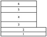
图1为本发明实施例1提出的基于有机-金属离子螯合电子传输层的有机光电探测器的结构示意图;1 is a schematic structural diagram of an organic photodetector based on an organic-metal ion chelated electron transport layer proposed in Example 1 of the present invention;
图2为本发明对比例1的电子传输层(PEIE)、实施例3的电子传输层(PEIE-Sn)和SnO2材料的N(1s)、O(1s)和Sn(3d)XPS曲线;2 is the N(1s), O(1s) and Sn(3d) XPS curves of the electron transport layer (PEIE) of Comparative Example 1, the electron transport layer (PEIE-Sn) of Example 3 and SnO2 materials of the present invention;
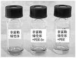
图3为本发明涉及的ITIC-Th(非富勒烯受体)溶液,PEIE溶液与ITIC-Th溶液的混合溶液,及实施例3的PEIE-Sn混合溶液与ITIC-Th溶液的混合溶液的反应实物图;Fig. 3 is the ITIC-Th (non-fullerene acceptor) solution involved in the present invention, the mixed solution of PEIE solution and ITIC-Th solution, and the mixed solution of PEIE-Sn mixed solution and ITIC-Th solution of Example 3. Reaction physical map;
图4为本发明实施例1~3和对比例1~3中制备在ITO上的电子传输层的AFM表面形貌图;Fig. 4 is the AFM surface topography of electron transport layers prepared on ITO in Examples 1-3 and Comparative Examples 1-3 of the present invention;
图5为本发明实施例1~3和对比例1~3所得有机光电探测器的J-V曲线,其中插图为放大的Jph-V曲线;5 is the JV curves of organic photodetectors obtained in Examples 1 to 3 and Comparative Examples 1 to 3 of the present invention, wherein the inset is an enlarged Jph -V curve;
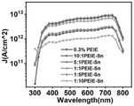
图6为本发明实施例1~3和对比例1~3所得有机光电探测器的D*-λ曲线;6 is the D*-λ curve of the organic photodetectors obtained in Examples 1-3 and Comparative Examples 1-3 of the present invention;
图7为本发明实施例2所得有机光电探测器的空气、紫外光稳定性的D*-λ曲线。7 is the D*-λ curve of the air and ultraviolet light stability of the organic photodetector obtained in Example 2 of the present invention.
附图标记如下:The reference numbers are as follows:
1-衬底,2-导电阴极,3-电子传输层,4-光活性层,5-空穴传输层,6-金属阳极。1-substrate, 2-conductive cathode, 3-electron transport layer, 4-photoactive layer, 5-hole transport layer, 6-metal anode.
具体实施方式Detailed ways
下面将结合本发明实施例中的附图,对本发明实施例中的技术方案进行清楚、完整地描述,显然,所描述的实施例仅仅是本发明一部分实施例,而不是全部的实施例。基于本发明中的实施例,本领域普通技术人员在没有做出创造性劳动前提下所获得的所有其他实施例,都属于本发明保护的范围。The technical solutions in the embodiments of the present invention will be clearly and completely described below with reference to the accompanying drawings in the embodiments of the present invention. Obviously, the described embodiments are only a part of the embodiments of the present invention, but not all of the embodiments. Based on the embodiments of the present invention, all other embodiments obtained by those of ordinary skill in the art without creative efforts shall fall within the protection scope of the present invention.
实施例1Example 1
本实施例提出了一种基于有机-金属离子螯合电子传输层的有机光电探测器,结构如图1所示,包括自下而上依次设置的衬底1、导电阴极2、电子传输层3、光活性层4、空穴传输层5和金属阳极6。This embodiment proposes an organic photodetector based on an organic-metal ion chelated electron transport layer. The structure is shown in FIG. 1 , including a
本实施例还提出上述有机光电探测器的制备方法,包括以下步骤:This embodiment also proposes a method for preparing the above organic photodetector, comprising the following steps:
步骤1:采用ITO作为由衬底1和导电阴极2共同组成的基板,对所述基板依次进行清洗、氮气吹干和紫外清洗;Step 1: ITO is used as the substrate composed of the
步骤2:将0.3wt%的PEIE溶液与15mg/ml的(Sn(CH3COO)2·4H2O溶液按照10:1的体积比混合,得到PEIE-Sn混合溶液,之后以5000rpm的转速旋涂40s于导电阴极2表面,经150℃热退火处理15min后,得到30nm厚的电子传输层(PEIE-Sn)3;Step2: Mix 0.3wt% PEIE solution with 15mg/ml (Sn(CH3COO)2·4H2O solution in a volume ratio of 10:1 to obtain a PEIE-Sn mixed solution, and then spin at 5000rpm Coated on the surface of the
步骤3:配制PBDB-T:ITIC-Th的质量比为1:1的、溶质浓度为30mg/mL的混合溶液,以2000rpm的转速旋涂40s于电子传输层3表面,经110℃热退火处理10min后,得到光活性层4;Step 3: Prepare a mixed solution with a mass ratio of PBDB-T:ITIC-Th of 1:1 and a solute concentration of 30 mg/mL, spin-coat on the surface of the
步骤4:在10-4Pa的真空度、650℃温度下,在光活性层4表面蒸镀MoO3,得到10nm厚的空穴传输层5,之后在空穴传输层5表面蒸镀100nm厚的金属阳极Ag,最后封装得到有机光电探测器。Step 4: Under the vacuum degree of 10−4 Pa and the temperature of 650° C., MoO3 is vapor-deposited on the surface of the
实施例2Example 2
本实施例提出了一种基于有机-金属离子螯合电子传输层的有机光电探测器的制备方法,与实施例1相比区别仅在于:将步骤2中0.3wt%的PEIE溶液与15mg/ml的(Sn(CH3COO)2·4H2O溶液的混合体积比调整为5:1;其他步骤不变。This example proposes a preparation method of an organic photodetector based on an organic-metal ion chelated electron transport layer. Compared with Example 1, the only difference is that the 0.3wt% PEIE solution in
实施例3Example 3
本实施例提出了一种基于有机-金属离子螯合电子传输层的有机光电探测器的制备方法,与实施例1相比区别仅在于:将步骤2中0.3wt%的PEIE溶液与15mg/ml的(Sn(CH3COO)2·4H2O溶液的混合体积比调整为1:1;其他步骤不变。This example proposes a preparation method of an organic photodetector based on an organic-metal ion chelated electron transport layer. Compared with Example 1, the only difference is that the 0.3wt% PEIE solution in
对比例1Comparative Example 1
本对比例提出了一种有机光电探测器的制备方法,与实施例1相比区别仅在于:步骤2中仅采用0.3wt%的PEIE溶液旋涂于导电阴极2表面,以制备电子传输层(PEIE);其他步骤不变。This comparative example proposes a preparation method of an organic photodetector. Compared with Example 1, the only difference is that in
对比例2Comparative Example 2
本对比例提出了一种有机光电探测器的制备方法,与实施例1相比区别仅在于:将步骤2中0.3wt%的PEIE溶液与15mg/ml的(Sn(CH3COO)2·4H2O溶液的混合体积比调整为1:5;其他步骤不变。This comparative example proposes a preparation method of an organic photodetector. Compared with Example 1, the only difference is: the 0.3wt% PEIE solution in
对比例3Comparative Example 3
本对比例提出了一种有机光电探测器的制备方法,与实施例1相比区别仅在于:将步骤2中0.3wt%的PEIE溶液与15mg/ml的(Sn(CH3COO)2·4H2O溶液的混合体积比调整为1:10;其他步骤不变。This comparative example proposes a preparation method of an organic photodetector. Compared with Example 1, the only difference is: the 0.3wt% PEIE solution in
本发明通过如图2所示的X射线光电子能谱(XPS)测量证实了PEIE与Sn2+之间存在螯合作用,具体为:如图2(a)所示,对比例1的电子传输层(PEIE)材料的N1s结合能为398.35eV,当引入Sn2+离子后,实施例1的电子传输层(PEIE-Sn)材料的N1s结合能右移,表明结合能增大;同理,如图2(c)所示,PEIE-Sn材料的Sn3d结合能相较于PEIE材料也有增大;而根据如图2(b)所示的O1s结合能可知,PEIE-Sn材料相较于PEIE材料,其O1s结合能更接近于SnO2材料,表明实施例1的电子传输层(PEIE-Sn)材料中可能有SnO2存在。进而表明PEIE-Sn材料的电子从PEIE中的N转移到Sn2+上,这种电子转移削弱了PEIE中胺的电负性,从而抑制了PEIE和ITIC-Th之间的化学反应,提高了光电探测器的性能。In the present invention, the X-ray photoelectron spectroscopy (XPS) measurement as shown in Figure 2 confirms the existence of chelation between PEIE and Sn2+ , specifically: as shown in Figure 2(a), the electron transport in Comparative Example 1 The N1s binding energy of the layer (PEIE) material is 398.35 eV. When Sn2+ ions are introduced, the N1s binding energy of the electron transport layer (PEIE-Sn) material of Example 1 shifts to the right, indicating that the binding energy increases; similarly, As shown in Figure 2(c), the Sn3d binding energy of PEIE-Sn material is also increased compared with PEIE material; and according to the O1s binding energy shown in Figure 2(b), PEIE-Sn material is compared with PEIE material. material, its O1s binding energy is closer to SnO2 material, indicating that SnO2 may exist in the electron transport layer (PEIE-Sn) material of Example 1. Furthermore, it is shown that the electrons of PEIE-Sn materials are transferred from N in PEIE to Sn2+ , and this electron transfer weakens the electronegativity of amines in PEIE, thereby inhibiting the chemical reaction between PEIE and ITIC-Th, improving the Photodetector performance.
根据如图3所示的ITIC-Th溶液,PEIE溶液与ITIC-Th溶液的混合溶液,及实施例3的PEIE-Sn混合溶液与ITIC-Th溶液的混合溶液的反应实物图,可知淡蓝色的ITIC-Th溶液在分别加入无色透明的PEIE溶液和PEIE-Sn混合溶液后,加入PEIE溶液的ITIC-Th溶液颜色由淡蓝色变为淡黄色,而加入PEIE-Sn混合溶液的ITIC-Th溶液颜色无变化,同样表明Sn2+的引入可以抑制PEIE和ITIC-Th之间的化学反应。According to the actual reaction diagram of the ITIC-Th solution, the mixed solution of the PEIE solution and the ITIC-Th solution, and the mixed solution of the PEIE-Sn mixed solution of Example 3 and the ITIC-Th solution as shown in Figure 3, it can be seen that the light blue After adding colorless and transparent PEIE solution and PEIE-Sn mixed solution respectively, the color of ITIC-Th solution added with PEIE solution changed from light blue to light yellow, while the color of ITIC-Th solution added with PEIE-Sn mixed solution changed from light blue to light yellow. There was no change in the color of the Th solution, which also indicated that the introduction of Sn2+ could inhibit the chemical reaction between PEIE and ITIC-Th.
对实施例1~3和对比例1~3中制备在ITO上的电子传输层进行AFM表面形貌表征,结果如图4所示,可知ITO基板的表面较为粗糙,其Rq=4.13nm,而在ITO表面制备一层由PEIE和Sn2+螯合得到的电子传输层PEIE-Sn后,粗糙度得到改善,并且实施例1~3中制得的电子传输层PEIE-Sn对ITO表面粗糙度的改善较为明显。The electron transport layers prepared on ITO in Examples 1-3 and Comparative Examples 1-3 were characterized by AFM surface morphology. The results are shown in Figure 4. It can be seen that the surface of the ITO substrate is relatively rough, and its Rq = 4.13nm, After preparing an electron transport layer PEIE-Sn obtained by chelating PEIE and Sn2+ on the surface of ITO, the roughness is improved, and the electron transport layer PEIE-Sn prepared in Examples 1 to 3 is rough on the surface of ITO The improvement is more obvious.
之后在光源300~800nm连续可调,-0.5V偏置电压的测试条件下,对实施例1~3和对比例1~3所得有机光电探测器进行光电测试,分别获得如图5所示的J-V曲线和如图6所示的D*-λ曲线。After that, under the test conditions of continuously adjustable light source 300-800nm and -0.5V bias voltage, photoelectric tests were carried out on the organic photodetectors obtained in Examples 1-3 and Comparative Examples 1-3, respectively, as shown in Figure 5. J-V curve and D*-λ curve as shown in Figure 6.
从J-V曲线可以看出,相较于对比例1中仅采用PEIE作为电子传输层,在PEIE中引入Sn2+发生螯合反应后,在保证光电流基本不变的同时抑制暗电流;尤其当实施例3中0.3wt%的PEIE溶液与15mg/ml的(Sn(CH3COO)2·4H2O溶液的混合体积比为1:1的情况,所得有机光电探测器的光电流还有一定增大。It can be seen from the JV curve that, compared with the use of PEIE as the electron transport layer in Comparative Example 1, the introduction of Sn2+ into PEIE and the chelation reaction can suppress the dark current while keeping the photocurrent basically unchanged. In Example 3, when the mixing volume ratio of 0.3 wt% PEIE solution and 15 mg/ml (Sn(CH3 COO)2 ·4H2 O solution is 1:1, the photocurrent of the obtained organic photodetector is still certain increase.
从D*-λ曲线可以看出,当选用如实施例1~3所示的混合体积比为(1、5或10):1的情形,可以很大程度提高有机光电探测器的D*,其中混合体积比为5:1的PEIE-Sn作为电子传输层的有机光电探测器(实施例2)的D*约是PEIE作为电子传输层的光电探测器(对比例1)的4倍。但是针对于对比例2和3中0.3wt%的PEIE溶液与15mg/ml的(Sn(CH3COO)2·4H2O溶液的混合体积比为1:(5或10)的情况,可能由于如图4所示的其表面粗糙度较大,界面接触较差导致器件的暗电流上升。It can be seen from the D*-λ curve that when the mixing volume ratio shown in Examples 1 to 3 is (1, 5 or 10):1, the D* of the organic photodetector can be greatly improved. The D* of the organic photodetector in which PEIE-Sn with a mixed volume ratio of 5:1 as the electron transport layer (Example 2) is about 4 times that of the photodetector with PEIE as the electron transport layer (Comparative Example 1). But for the case where the mixing volume ratio of 0.3wt% PEIE solution and 15mg/ml (Sn(CH3COO)2· 4H2O solution is 1:(5 or 10) in Comparative Examples 2 and3 , it may be due to As shown in Figure 4, the surface roughness is large, and the interface contact is poor, which leads to the increase of the dark current of the device.
进一步对实施例2所制备的有机光电探测器进行空气稳定性和紫外稳定性测试。紫外稳定性的测试条件:未封装器件直接暴露在空气(相对湿度平均=40%)中,用340nm紫外光持续照射数小时,随后进行光电测试获得如图7(a)所示的D*-λ曲线。空气稳定性的存储条件:未封装器件直接暴露在空气(相对湿度平均=40%)中数小时,随后进行光电测试获得如图7(b)所示的D*-λ曲线。从7(a)曲线可以看出,器件紫外光照射下其D*衰减较少。从7(b)曲线可以看出,器件暴露在空气中100h,其仍然保持较高的D*。The organic photodetector prepared in Example 2 was further tested for air stability and ultraviolet stability. Test conditions for UV stability: the unpackaged device was directly exposed to the air (average relative humidity = 40%), continuously irradiated with 340 nm UV light for several hours, and then subjected to photoelectric testing to obtain D*- as shown in Figure 7(a). λ curve. Storage conditions for air stability: The unpackaged device was directly exposed to air (average relative humidity = 40%) for several hours, followed by photoelectric testing to obtain the D*-λ curve shown in Figure 7(b). It can be seen from the curve 7(a) that the D* decay of the device is less under UV light irradiation. It can be seen from curve 7(b) that the device still maintains a high D* when exposed to air for 100 h.
最后应说明的是:以上实施例仅用以说明本发明的技术方案,而非对其限制;尽管参照前述实施例对本发明进行了详细的说明,本领域的普通技术人员应当理解:其依然可以对前述实施例所记载的技术方案进行修改,或者对其中部分或者全部技术特征进行等同替换;而这些修改或者替换,并不使相应技术方案的本质脱离本发明实施例技术方案的范围,其均应涵盖在本发明的权利要求和说明书的范围当中。Finally, it should be noted that the above embodiments are only used to illustrate the technical solutions of the present invention, but not to limit them; although the present invention has been described in detail with reference to the foregoing embodiments, those of ordinary skill in the art should understand that it can still be Modifications are made to the technical solutions recorded in the foregoing embodiments, or some or all of the technical features thereof are equivalently replaced; and these modifications or replacements do not make the essence of the corresponding technical solutions deviate from the scope of the technical solutions of the embodiments of the present invention. It should be covered within the scope of the claims and description of the present invention.
Claims (6)
Priority Applications (1)
| Application Number | Priority Date | Filing Date | Title |
|---|---|---|---|
| CN202111633250.5ACN114512615A (en) | 2021-12-29 | 2021-12-29 | Organic photoelectric detector based on organic-metal ion chelated electron transport layer |
Applications Claiming Priority (1)
| Application Number | Priority Date | Filing Date | Title |
|---|---|---|---|
| CN202111633250.5ACN114512615A (en) | 2021-12-29 | 2021-12-29 | Organic photoelectric detector based on organic-metal ion chelated electron transport layer |
Publications (1)
| Publication Number | Publication Date |
|---|---|
| CN114512615Atrue CN114512615A (en) | 2022-05-17 |
Family
ID=81547789
Family Applications (1)
| Application Number | Title | Priority Date | Filing Date |
|---|---|---|---|
| CN202111633250.5APendingCN114512615A (en) | 2021-12-29 | 2021-12-29 | Organic photoelectric detector based on organic-metal ion chelated electron transport layer |
Country Status (1)
| Country | Link |
|---|---|
| CN (1) | CN114512615A (en) |
Citations (8)
| Publication number | Priority date | Publication date | Assignee | Title |
|---|---|---|---|---|
| US5091278A (en)* | 1990-08-31 | 1992-02-25 | Xerox Corporation | Blocking layer for photoreceptors |
| CN1649184A (en)* | 2005-03-04 | 2005-08-03 | 友达光电股份有限公司 | Organic light emitting diode and display device including the organic light emitting diode |
| CN104183726A (en)* | 2013-05-21 | 2014-12-03 | 海洋王照明科技股份有限公司 | Organic light emission diode and preparation method thereof |
| CN110518123A (en)* | 2019-07-26 | 2019-11-29 | 西安电子科技大学 | Using composite material as the perovskite solar battery and preparation method of electron transfer layer |
| CN111081885A (en)* | 2018-10-19 | 2020-04-28 | 华中科技大学 | A polymer-metal chelate cathode interface material and its application |
| CN111490167A (en)* | 2020-04-24 | 2020-08-04 | 电子科技大学 | A near-infrared flexible detector based on optical microcavity effect and its preparation method |
| CN111740018A (en)* | 2020-07-07 | 2020-10-02 | 吉林大学 | A broadband, low-noise, ultra-fast response organic photodetector with cascade structure and preparation method thereof |
| CN111952454A (en)* | 2020-07-28 | 2020-11-17 | 电子科技大学 | An organic photodetector based on a hybrid electron transport layer and its preparation method |
- 2021
- 2021-12-29CNCN202111633250.5Apatent/CN114512615A/enactivePending
Patent Citations (8)
| Publication number | Priority date | Publication date | Assignee | Title |
|---|---|---|---|---|
| US5091278A (en)* | 1990-08-31 | 1992-02-25 | Xerox Corporation | Blocking layer for photoreceptors |
| CN1649184A (en)* | 2005-03-04 | 2005-08-03 | 友达光电股份有限公司 | Organic light emitting diode and display device including the organic light emitting diode |
| CN104183726A (en)* | 2013-05-21 | 2014-12-03 | 海洋王照明科技股份有限公司 | Organic light emission diode and preparation method thereof |
| CN111081885A (en)* | 2018-10-19 | 2020-04-28 | 华中科技大学 | A polymer-metal chelate cathode interface material and its application |
| CN110518123A (en)* | 2019-07-26 | 2019-11-29 | 西安电子科技大学 | Using composite material as the perovskite solar battery and preparation method of electron transfer layer |
| CN111490167A (en)* | 2020-04-24 | 2020-08-04 | 电子科技大学 | A near-infrared flexible detector based on optical microcavity effect and its preparation method |
| CN111740018A (en)* | 2020-07-07 | 2020-10-02 | 吉林大学 | A broadband, low-noise, ultra-fast response organic photodetector with cascade structure and preparation method thereof |
| CN111952454A (en)* | 2020-07-28 | 2020-11-17 | 电子科技大学 | An organic photodetector based on a hybrid electron transport layer and its preparation method |
Similar Documents
| Publication | Publication Date | Title |
|---|---|---|
| Huang et al. | Water‐resistant and flexible perovskite solar cells via a glued interfacial layer | |
| Feng et al. | Record efficiency stable flexible perovskite solar cell using effective additive assistant strategy | |
| CN111952454B (en) | An organic photodetector based on a hybrid electron transport layer and its preparation method | |
| Lee et al. | Investigation of charge carrier behavior in high performance ternary blend polymer solar cells | |
| CN110492000B (en) | A kind of perovskite photodetector based on sodium alginate cross-linked photoactive layer and preparation method thereof | |
| Qian et al. | Multifunctional effect of p‐doping, antireflection, and encapsulation by polymeric acid for high efficiency and stable carbon nanotube‐based silicon solar cells | |
| Zhen et al. | An ethanolamine-functionalized fullerene as an efficient electron transport layer for high-efficiency inverted polymer solar cells | |
| CN109920918B (en) | Perovskite photoelectric detector based on composite electron transport layer and preparation method thereof | |
| CN109585660B (en) | Perovskite photoelectric detector based on organic-inorganic hybrid double passivation layers and preparation method thereof | |
| CN110504368B (en) | An organic photodetector based on a hybrid hole transport layer and its preparation method | |
| Balasaravanan et al. | Triphenylamine (TPA)‐functionalized structural isomeric polythiophenes as dopant free hole‐transporting materials for tin perovskite solar cells | |
| Zhao et al. | Molecular modulator for stable inverted planar perovskite solar cells with efficiency enhanced by interface engineering | |
| Liu et al. | A cross‐linked interconnecting layer enabling reliable and reproducible solution‐processing of organic tandem solar cells | |
| CN111933807B (en) | A highly stable perovskite photodetector prepared based on additive treatment and preparation method thereof | |
| CN109879761B (en) | Non-lead perovskite photoelectric functional material, solar cell, and preparation method and application of material | |
| CN110473971A (en) | One kind is based on organic wide spectrum photodetector of ternary and preparation method thereof | |
| CN111785837A (en) | A kind of tin-based perovskite thin film and its preparation method and application | |
| CN109326723B (en) | A kind of organic photodetector based on magnetic field effect spin coating process and preparation method | |
| CN111162173B (en) | An organic photodetector with a doped electron transport layer and its preparation method | |
| AL-Amar et al. | A new method to improve the lifetime stability of small molecule bilayer heterojunction organic solar cells | |
| CN109360892A (en) | A visible-near-infrared wide-spectrum detection device using high-response perovskite/polymer hybrid film and its preparation method | |
| Yang et al. | Aqueous solution‐processed NiOx anode buffer layers applicable for polymer solar cells | |
| Wijaya et al. | A Highly Stable Organic–Inorganic Hybrid Electron Transport Layer for Ultraflexible Organic Photodiodes | |
| CN113072589B (en) | A class of fluoroboron dipyrrole derivatives, preparation method and photodetector using the same as donor doped | |
| CN110492001A (en) | A kind of organic photodetector and preparation method thereof based on spin coating heating process |
Legal Events
| Date | Code | Title | Description |
|---|---|---|---|
| PB01 | Publication | ||
| PB01 | Publication | ||
| SE01 | Entry into force of request for substantive examination | ||
| SE01 | Entry into force of request for substantive examination | ||
| RJ01 | Rejection of invention patent application after publication | Application publication date:20220517 | |
| RJ01 | Rejection of invention patent application after publication |