CN114512447A - Semiconductor device and method of making the same - Google Patents
Semiconductor device and method of making the sameDownload PDFInfo
- Publication number
- CN114512447A CN114512447ACN202011170771.7ACN202011170771ACN114512447ACN 114512447 ACN114512447 ACN 114512447ACN 202011170771 ACN202011170771 ACN 202011170771ACN 114512447 ACN114512447 ACN 114512447A
- Authority
- CN
- China
- Prior art keywords
- semiconductor device
- integrated circuit
- sealing ring
- semiconductor substrate
- fingers
- Prior art date
- Legal status (The legal status is an assumption and is not a legal conclusion. Google has not performed a legal analysis and makes no representation as to the accuracy of the status listed.)
- Granted
Links
- 239000004065semiconductorSubstances0.000titleclaimsabstractdescription93
- 238000004519manufacturing processMethods0.000titleclaimsdescription8
- 238000007789sealingMethods0.000claimsabstractdescription107
- 239000000758substrateSubstances0.000claimsabstractdescription49
- 238000000034methodMethods0.000claimsabstractdescription41
- 230000004888barrier functionEffects0.000claimsdescription16
- 230000008569processEffects0.000description24
- 229910052751metalInorganic materials0.000description11
- 239000002184metalSubstances0.000description11
- 150000001875compoundsChemical class0.000description7
- 230000005669field effectEffects0.000description6
- 239000012212insulatorSubstances0.000description6
- 150000002500ionsChemical class0.000description6
- 238000005530etchingMethods0.000description5
- 239000000463materialSubstances0.000description5
- 230000001902propagating effectEffects0.000description5
- 230000001681protective effectEffects0.000description5
- XUIMIQQOPSSXEZ-UHFFFAOYSA-NSiliconChemical compound[Si]XUIMIQQOPSSXEZ-UHFFFAOYSA-N0.000description4
- 229910052710siliconInorganic materials0.000description4
- 239000010703siliconSubstances0.000description4
- 229910000577Silicon-germaniumInorganic materials0.000description3
- LEVVHYCKPQWKOP-UHFFFAOYSA-N[Si].[Ge]Chemical compound[Si].[Ge]LEVVHYCKPQWKOP-UHFFFAOYSA-N0.000description3
- 230000009286beneficial effectEffects0.000description3
- 230000000694effectsEffects0.000description3
- 229910052732germaniumInorganic materials0.000description3
- GNPVGFCGXDBREM-UHFFFAOYSA-Ngermanium atomChemical compound[Ge]GNPVGFCGXDBREM-UHFFFAOYSA-N0.000description3
- 229910044991metal oxideInorganic materials0.000description3
- 150000004706metal oxidesChemical class0.000description3
- 238000001020plasma etchingMethods0.000description3
- 238000000992sputter etchingMethods0.000description3
- JBRZTFJDHDCESZ-UHFFFAOYSA-NAsGaChemical compound[As]#[Ga]JBRZTFJDHDCESZ-UHFFFAOYSA-N0.000description2
- 229910001218Gallium arsenideInorganic materials0.000description2
- 229910000673Indium arsenideInorganic materials0.000description2
- GPXJNWSHGFTCBW-UHFFFAOYSA-NIndium phosphideChemical compound[In]#PGPXJNWSHGFTCBW-UHFFFAOYSA-N0.000description2
- 238000000231atomic layer depositionMethods0.000description2
- 239000003990capacitorSubstances0.000description2
- 238000005229chemical vapour depositionMethods0.000description2
- 238000007772electroless platingMethods0.000description2
- 238000009713electroplatingMethods0.000description2
- 230000006870functionEffects0.000description2
- RPQDHPTXJYYUPQ-UHFFFAOYSA-Nindium arsenideChemical compound[In]#[As]RPQDHPTXJYYUPQ-UHFFFAOYSA-N0.000description2
- 239000000203mixtureSubstances0.000description2
- 238000005240physical vapour depositionMethods0.000description2
- 238000000623plasma-assisted chemical vapour depositionMethods0.000description2
- HBMJWWWQQXIZIP-UHFFFAOYSA-Nsilicon carbideChemical compound[Si+]#[C-]HBMJWWWQQXIZIP-UHFFFAOYSA-N0.000description2
- 229910010271silicon carbideInorganic materials0.000description2
- 238000004528spin coatingMethods0.000description2
- 229910005540GaPInorganic materials0.000description1
- NRTOMJZYCJJWKI-UHFFFAOYSA-NTitanium nitrideChemical compound[Ti]#NNRTOMJZYCJJWKI-UHFFFAOYSA-N0.000description1
- 239000002253acidSubstances0.000description1
- 239000003513alkaliSubstances0.000description1
- 229910052782aluminiumInorganic materials0.000description1
- XAGFODPZIPBFFR-UHFFFAOYSA-NaluminiumChemical compound[Al]XAGFODPZIPBFFR-UHFFFAOYSA-N0.000description1
- QVGXLLKOCUKJST-UHFFFAOYSA-Natomic oxygenChemical compound[O]QVGXLLKOCUKJST-UHFFFAOYSA-N0.000description1
- 239000002585baseSubstances0.000description1
- 230000015572biosynthetic processEffects0.000description1
- 230000008859changeEffects0.000description1
- 238000004140cleaningMethods0.000description1
- 238000000151depositionMethods0.000description1
- 238000001312dry etchingMethods0.000description1
- 238000009837dry grindingMethods0.000description1
- 238000009472formulationMethods0.000description1
- HZXMRANICFIONG-UHFFFAOYSA-Ngallium phosphideChemical compound[Ga]#PHZXMRANICFIONG-UHFFFAOYSA-N0.000description1
- 239000007789gasSubstances0.000description1
- 238000000227grindingMethods0.000description1
- 238000002513implantationMethods0.000description1
- WPYVAWXEWQSOGY-UHFFFAOYSA-Nindium antimonideChemical compound[Sb]#[In]WPYVAWXEWQSOGY-UHFFFAOYSA-N0.000description1
- 238000012986modificationMethods0.000description1
- 230000004048modificationEffects0.000description1
- 229910021421monocrystalline siliconInorganic materials0.000description1
- 230000035772mutationEffects0.000description1
- 239000002135nanosheetSubstances0.000description1
- 239000002070nanowireSubstances0.000description1
- 239000001301oxygenSubstances0.000description1
- 229910052760oxygenInorganic materials0.000description1
- 229920002120photoresistant polymerPolymers0.000description1
- 238000005498polishingMethods0.000description1
- 230000002265preventionEffects0.000description1
- 238000000926separation methodMethods0.000description1
- 239000002904solventSubstances0.000description1
- 238000004544sputter depositionMethods0.000description1
- 230000003068static effectEffects0.000description1
- 239000000126substanceSubstances0.000description1
- WFKWXMTUELFFGS-UHFFFAOYSA-NtungstenChemical compound[W]WFKWXMTUELFFGS-UHFFFAOYSA-N0.000description1
- 229910052721tungstenInorganic materials0.000description1
- 239000010937tungstenSubstances0.000description1
- 238000001039wet etchingMethods0.000description1
Images


Classifications
- H—ELECTRICITY
- H01—ELECTRIC ELEMENTS
- H01L—SEMICONDUCTOR DEVICES NOT COVERED BY CLASS H10
- H01L23/00—Details of semiconductor or other solid state devices
- H01L23/562—Protection against mechanical damage
- H—ELECTRICITY
- H01—ELECTRIC ELEMENTS
- H01L—SEMICONDUCTOR DEVICES NOT COVERED BY CLASS H10
- H01L21/00—Processes or apparatus adapted for the manufacture or treatment of semiconductor or solid state devices or of parts thereof
- H01L21/70—Manufacture or treatment of devices consisting of a plurality of solid state components formed in or on a common substrate or of parts thereof; Manufacture of integrated circuit devices or of parts thereof
- H01L21/77—Manufacture or treatment of devices consisting of a plurality of solid state components or integrated circuits formed in, or on, a common substrate
- H—ELECTRICITY
- H01—ELECTRIC ELEMENTS
- H01L—SEMICONDUCTOR DEVICES NOT COVERED BY CLASS H10
- H01L23/00—Details of semiconductor or other solid state devices
- H—ELECTRICITY
- H01—ELECTRIC ELEMENTS
- H01L—SEMICONDUCTOR DEVICES NOT COVERED BY CLASS H10
- H01L23/00—Details of semiconductor or other solid state devices
- H01L23/564—Details not otherwise provided for, e.g. protection against moisture
Landscapes
- Engineering & Computer Science (AREA)
- Physics & Mathematics (AREA)
- Condensed Matter Physics & Semiconductors (AREA)
- General Physics & Mathematics (AREA)
- Computer Hardware Design (AREA)
- Microelectronics & Electronic Packaging (AREA)
- Power Engineering (AREA)
- Manufacturing & Machinery (AREA)
- Semiconductor Integrated Circuits (AREA)
Abstract
Translated fromChinese
Description
Translated fromChinese技术领域technical field
本发明总体来说涉及半导体技术领域,具体而言,涉及一种半导体装置及其制作方法。The present invention generally relates to the technical field of semiconductors, and in particular, to a semiconductor device and a method for fabricating the same.
背景技术Background technique
半导体集成电路产业已经历快速成长。随着半导体器件的尺寸不断减小,对芯片外围的密封环所起到防止湿气、离子进入芯片内部以及防止裂缝向芯片内传播的作用的要求越来越高。然而,现有技术中的密封环的防护效果并不理想。The semiconductor integrated circuit industry has experienced rapid growth. As the size of semiconductor devices continues to decrease, the requirements for the sealing ring around the chip to prevent moisture and ions from entering the chip and preventing cracks from propagating into the chip are getting higher and higher. However, the protective effect of the sealing ring in the prior art is not ideal.
发明内容SUMMARY OF THE INVENTION
本发明实施例提供的半导体装置及其制作方法,其密封环的防护效果更强。In the semiconductor device and the manufacturing method thereof provided by the embodiments of the present invention, the protection effect of the sealing ring is stronger.
本发明实施例的半导体装置,包括半导体基底、形成在所述半导体基底中的集成电路区域以及一个或多个密封环,一个或多个密封环设于所述半导体基底中,且围绕所述集成电路区域的周边布置,用以防护所述集成电路区域;其中,所述密封环具有波浪形结构。A semiconductor device according to an embodiment of the present invention includes a semiconductor substrate, an integrated circuit region formed in the semiconductor substrate, and one or more sealing rings, wherein the one or more sealing rings are provided in the semiconductor substrate and surround the integrated circuit The periphery of the circuit area is arranged to protect the integrated circuit area; wherein, the sealing ring has a wavy structure.
在其中一个实施方式中,所述密封环包括多个波峰部和多个波谷部,多个所述波峰部和多个所述波谷部交替设置,每个所述波峰部朝所述集成电路区域的方向凸设,每个所述波谷部朝背离所述集成电路区域的方向凸设。In one embodiment, the sealing ring includes a plurality of crests and a plurality of troughs, a plurality of the crests and a plurality of the troughs are alternately arranged, and each of the crests faces the integrated circuit region and each of the valleys is protruded in a direction away from the integrated circuit region.
在其中一个实施方式中,多个所述波峰部的曲率相同,多个所述波谷部的曲率相同。In one of the embodiments, the plurality of crest portions have the same curvature, and the plurality of the trough portions have the same curvature.
在其中一个实施方式中,每个所述波峰部与每个所述波谷部的曲率相同。In one of the embodiments, each of the peaks and each of the troughs have the same curvature.
在其中一个实施方式中,所述密封环的数量为至少两个。In one of the embodiments, the number of the sealing rings is at least two.
在其中一个实施方式中,相邻的两个所述密封环的其中一个所述密封环的多个所述波峰部与另一个所述密封环的多个波峰部对应设置;In one of the embodiments, a plurality of the wave crest portions of one of the two adjacent seal rings are arranged corresponding to the wave crest portions of the other seal ring;
相邻的两个所述密封环的其中一个所述密封环的多个所述波谷部与另一个所述密封环的多个波谷部对应设置。The plurality of trough portions of one of the two adjacent seal rings are arranged corresponding to the plurality of trough portions of the other seal ring.
在其中一个实施方式中,相邻的两个所述密封环的其中一个所述密封环的多个所述波峰部与另一个所述密封环的多个波谷部对应设置;In one of the embodiments, a plurality of the wave crest portions of one of the two adjacent sealing rings are arranged corresponding to the plurality of wave troughs of the other sealing ring;
相邻的两个所述密封环的其中一个所述密封环的多个所述波谷部与另一个所述密封环的多个波峰部对应设置。The plurality of trough portions of one of the two adjacent seal rings are arranged corresponding to the plurality of crest portions of the other seal ring.
在其中一个实施方式中,所述密封环的数量为至少两个,相邻的两个所述密封环的其中一个所述密封环包括多个指状部,所述指状部朝向另一个所述密封环的方向延伸。In one of the embodiments, the number of the sealing rings is at least two, and one of the two adjacent sealing rings includes a plurality of fingers, the fingers facing the other. extend in the direction of the sealing ring.
在其中一个实施方式中,所述指状部连接于相邻的两个所述密封环,以使至少两个所述密封环形成一网状结构。In one embodiment, the fingers are connected to two adjacent sealing rings, so that at least two of the sealing rings form a network structure.
在其中一个实施方式中,所述指状部具有弧形表面,所述弧形表面朝向另一个所述密封环。In one of the embodiments, the fingers have arcuate surfaces facing the other of the sealing rings.
在其中一个实施方式中,所述半导体装置还包括阻挡层,所述阻挡层设于所述半导体基底和所述密封环之间。In one embodiment, the semiconductor device further includes a barrier layer disposed between the semiconductor substrate and the seal ring.
本发明实施例的半导体装置的制作方法,包括如下步骤:The manufacturing method of the semiconductor device according to the embodiment of the present invention includes the following steps:
提供一具有集成电路区域的半导体基底;providing a semiconductor substrate having an integrated circuit region;
在所述半导体基底上形成一个或多个沟槽,所述沟槽围绕所述集成电路区域的周边布置;以及forming one or more trenches in the semiconductor substrate, the trenches being arranged around the perimeter of the integrated circuit region; and
在所述一个或多个沟槽内形成一个或多个密封环,所述密封环具有波浪形结构。One or more sealing rings are formed within the one or more grooves, the sealing rings having a wavy configuration.
在其中一个实施方式中,在所述一个或多个沟槽内形成一个或多个密封环之前,所述方法还包括:In one embodiment, prior to forming one or more seal rings in the one or more grooves, the method further comprises:
形成与所述沟槽表面共形的阻挡层。A barrier layer is formed conformal to the trench surface.
在其中一个实施方式中,所述密封环包括多个波峰部和多个波谷部,多个所述波峰部和多个所述波谷部交替设置,每个所述波峰部朝所述集成电路区域的方向凸设,每个所述波谷部朝背离所述集成电路区域的方向凸设。In one embodiment, the sealing ring includes a plurality of crests and a plurality of troughs, a plurality of the crests and a plurality of the troughs are alternately arranged, and each of the crests faces the integrated circuit region and each of the valleys is protruded in a direction away from the integrated circuit region.
在其中一个实施方式中,多个所述波峰部的曲率相同,多个所述波谷部的曲率相同。In one of the embodiments, the plurality of crest portions have the same curvature, and the plurality of the trough portions have the same curvature.
在其中一个实施方式中,每个所述波峰部与每个所述波谷部的曲率相同。In one of the embodiments, each of the peaks and each of the troughs have the same curvature.
在其中一个实施方式中,所述密封环的数量为至少两个。In one of the embodiments, the number of the sealing rings is at least two.
在其中一个实施方式中,相邻的两个所述密封环的其中一个所述密封环的多个所述波峰部与另一个所述密封环的多个波峰部对应设置;In one of the embodiments, a plurality of the wave crest portions of one of the two adjacent seal rings are arranged corresponding to the wave crest portions of the other seal ring;
相邻的两个所述密封环的其中一个所述密封环的多个所述波谷部与另一个所述密封环的多个波谷部对应设置。The plurality of trough portions of one of the two adjacent seal rings are arranged corresponding to the plurality of trough portions of the other seal ring.
在其中一个实施方式中,相邻的两个所述密封环的其中一个所述密封环的多个所述波峰部与另一个所述密封环的多个波谷部对应设置;In one of the embodiments, a plurality of the wave crest portions of one of the two adjacent sealing rings are arranged corresponding to the plurality of wave troughs of the other sealing ring;
相邻的两个所述密封环的其中一个所述密封环的多个所述波谷部与另一个所述密封环的多个波峰部对应设置。The plurality of trough portions of one of the two adjacent seal rings are arranged corresponding to the plurality of crest portions of the other seal ring.
在其中一个实施方式中,所述密封环的数量为至少两个,相邻的两个所述密封环的其中一个所述密封环包括多个指状部,所述指状部朝向另一个所述密封环的方向延伸。In one of the embodiments, the number of the sealing rings is at least two, and one of the two adjacent sealing rings includes a plurality of fingers, the fingers facing the other. extend in the direction of the sealing ring.
在其中一个实施方式中,所述指状部连接于相邻的两个所述密封环,以使至少两个所述密封环形成一网状结构。In one embodiment, the fingers are connected to two adjacent sealing rings, so that at least two of the sealing rings form a network structure.
在其中一个实施方式中,所述指状部具有弧形表面,所述弧形表面朝向另一个所述密封环。In one of the embodiments, the fingers have arcuate surfaces facing the other of the sealing rings.
上述发明中的一个实施例具有如下优点或有益效果:An embodiment of the above invention has the following advantages or beneficial effects:
本发明实施例的密封环具有波浪形结构,该波浪形结构使密封环朝向集成电路区域方向的表面以及背离集成电路区域的方向的表面均呈弧形,弧形表面相比平面具有更大的拦截面积,使本发明实施例的密封环能够更加有效地防止湿气和离子进入集成电路区域内以及防止裂缝朝向集成电路区域内传播,显著提高了密封环的防护作用。The sealing ring of the embodiment of the present invention has a wave-shaped structure, and the wave-shaped structure makes the surface of the sealing ring in the direction of the integrated circuit area and the surface in the direction away from the integrated circuit area are arc-shaped, and the arc-shaped surface has a larger surface than a flat surface. The intercepting area enables the sealing ring of the embodiment of the present invention to more effectively prevent moisture and ions from entering the integrated circuit area and prevent cracks from propagating toward the integrated circuit area, which significantly improves the protective effect of the sealing ring.
附图说明Description of drawings
通过参照附图详细描述其示例实施方式,本发明的上述和其它特征及优点将变得更加明显。The above and other features and advantages of the present invention will become more apparent from the detailed description of example embodiments thereof with reference to the accompanying drawings.
图1示出的是本发明实施例的半导体装置的剖视图。FIG. 1 is a cross-sectional view of a semiconductor device according to an embodiment of the present invention.
图2示出的是图1中K处的第一实施例的局部放大图。FIG. 2 shows a partial enlarged view of the first embodiment at K in FIG. 1 .
图3示出的是图1中K处的第二实施例的局部放大图。FIG. 3 shows a partial enlarged view of the second embodiment at K in FIG. 1 .
图4示出的是图3中L处的指状部的一实施方式的局部放大图。FIG. 4 shows a partial enlarged view of an embodiment of the finger at L in FIG. 3 .
图5示出的是图1中K处的第三实施例的局部放大图。FIG. 5 shows a partial enlarged view of the third embodiment at K in FIG. 1 .
图6示出的是图1中K处的第四实施例的局部放大图。FIG. 6 shows a partial enlarged view of the fourth embodiment at K in FIG. 1 .
图7至13示出的是本发明实施例的半导体装置的制作方法的不同工艺阶段的剖视图,其中图7至图11示出的是图2中沿A-A的剖视图,图12和图13示出的是图5中沿B-B的剖视图。FIGS. 7 to 13 are cross-sectional views of different process stages of a method for fabricating a semiconductor device according to an embodiment of the present invention, wherein FIGS. 7 to 11 are cross-sectional views along the line A-A in FIG. 2 , and FIGS. 12 and 13 show The sectional view taken along the line B-B in FIG. 5 is shown.
其中,附图标记说明如下:Among them, the reference numerals are described as follows:
100、半导体基底 110、集成电路区域100.
120、沟槽 200、密封环120,
201、空间 210、指状部201.
211、弧形表面 220、波峰部211,
230、波谷部 300、掩模层230,
400、阻挡层 500、金属层400,
具体实施方式Detailed ways
现在将参考附图更全面地描述示例实施方式。然而,示例实施方式能够以多种形式实施,且不应被理解为限于在此阐述的实施方式;相反,提供这些实施方式使得本发明将全面和完整,并将示例实施方式的构思全面地传达给本领域的技术人员。图中相同的附图标记表示相同或类似的结构,因而将省略它们的详细描述。Example embodiments will now be described more fully with reference to the accompanying drawings. Example embodiments, however, can be embodied in various forms and should not be construed as limited to the embodiments set forth herein; rather, these embodiments are provided so that this disclosure will be thorough and complete, and will fully convey the concept of example embodiments to those skilled in the art. The same reference numerals in the drawings denote the same or similar structures, and thus their detailed descriptions will be omitted.
半导体装置通常设置有密封环,该密封环围绕半导体装置的集成电路区域的外周延伸。密封环通常是一个或多个金属层的连续环。在一个或多个示例实施例中,密封环可以具有以下一项或多项功能:提供防护以防止外界湿气进入形成在半导体装置的中集成电路组件。提供防护以防止离子侵入形成在衬底中的集成电路部件,并提供防护结构以防止裂缝在衬底中朝向密封环向内的集成电路部件所在的区域的传播。Semiconductor devices are typically provided with a seal ring that extends around the periphery of the integrated circuit region of the semiconductor device. The sealing ring is usually a continuous ring of one or more metal layers. In one or more example embodiments, the seal ring may have one or more of the following functions: provide protection from outside moisture from entering integrated circuit components formed in the semiconductor device. Shielding is provided to prevent ion intrusion into integrated circuit components formed in the substrate, and a shielding structure is provided to prevent propagation of cracks in the substrate toward areas where the integrated circuit components are located inwardly of the seal ring.
本发明实施例可用于采用密封环的任何合适的半导体装置,比如互补式金属氧化物半导体场效晶体管、互补式金属氧化物半导体装置、p型金属氧化物半导体装置、n型金属氧化物半导体装置、鳍状场效晶体管、全绕式栅极金属氧化物半导体场效晶体管如纳米线装置或纳米片装置、或其他多栅极场效晶体管。在集成电路或其部分(其可包含静态随机存取存储器及/或逻辑电路、无源构件如电阻、电容、或电感、与有源构件如p型场效晶体管、n型场效晶体管、鳍状场效晶体管、互补式金属氧化物半导体场效晶体管、互补式金属氧化物半导体晶体管、双极晶体管、高电压晶体管、高频晶体管、其他存储器单元、或上述的组合)的加工时,可制作半导体装置。Embodiments of the present invention may be used in any suitable semiconductor device that employs a seal ring, such as CMOS field effect transistors, CMOS devices, p-type metal oxide semiconductor devices, n-type metal oxide semiconductor devices , fin field effect transistors, fully wound gate metal oxide semiconductor field effect transistors such as nanowire devices or nanosheet devices, or other multi-gate field effect transistors. In integrated circuits or portions thereof (which may include static random access memory and/or logic circuits, passive components such as resistors, capacitors, or inductors, and active components such as p-type field effect transistors, n-type field effect transistors, fins MOSFETs, CMOS FETs, CMOS transistors, bipolar transistors, high-voltage transistors, high-frequency transistors, other memory cells, or a combination of the above) can be fabricated semiconductor device.
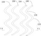
如图1所示,图1示出的是本发明实施例的半导体装置的剖视图。本发明实施例的半导体装置包括半导体基底100、形成在半导体基底100中的集成电路区域110以及多个密封环200,多个密封环200设于半导体基底100中,且围绕集成电路区域110的周边布置,用以防护集成电路区域110。其中,密封环200具有波浪形结构。As shown in FIG. 1 , FIG. 1 shows a cross-sectional view of a semiconductor device according to an embodiment of the present invention. The semiconductor device according to the embodiment of the present invention includes a
集成电路区域110内可以设有一个或多个有源器件(例如,晶体管、二极管、光二极管等)、一个或多个无源器件(例如,电阻器、电容器、电感器等)、或上述的组合。Integrated
多个密封环200围绕在集成电路区域110的周边,至少实现如下一种功能:防止湿气进入形成在集成电路区域110的衬底中的集成电路元件、防止离子进入衬底中形成的集成电路元件,以及防止衬底中的裂缝朝向集成电路元件所在的密封环200的内部区域传播。The plurality of sealing
相比现有技术中的密封环的形状,本发明实施例的密封环200具有波浪形结构,该波浪形结构使密封环200朝向集成电路区域110方向的表面以及背离集成电路区域110的方向的表面均呈弧形表面,弧形表面相比平面具有更大的拦截面积,使本发明实施例的密封环200能够更加有效地防止湿气和离子进入集成电路区域110内以及防止裂缝朝向集成电路区域110内传播,显著提高了密封环200的防护作用。Compared with the shape of the sealing ring in the prior art, the sealing
如图2所示,图2示出的是图1中K处的第一实施例的局部放大图。本发明实施例的半导体装置包括四个密封环200,围绕集成电路区域110的周边依次布置。As shown in FIG. 2 , FIG. 2 shows a partial enlarged view of the first embodiment at K in FIG. 1 . The semiconductor device according to the embodiment of the present invention includes four sealing
本发明实施例的密封环200包括多个波峰部220和多个波谷部230,多个波峰部220和多个波谷部230交替设置,每个波峰部220朝集成电路区域110的方向凸设,每个波谷部230朝背离集成电路区域110的方向凸设。多个波峰部220的曲率相同,多个波谷部230的曲率相同。每个波峰部220与每个波谷部230的曲率相同。The sealing
通过上述密封环200的多个波峰部220和多个波谷部230的形状相同且曲率相同的设计,使得每个密封环200的每处波峰部220和每处波谷部230的拦截面积大致相同且均匀,避免出现拦截面积不一致产生突变而引发结构强度不同,最终导致突变处易发生损坏。另外,密封环200的结构相同且均匀还便于加工。Through the design of the plurality of
当然,可以理解的是,上述的密封环200的多个波峰部220和多个波谷部230还可以采用如下变形结构,例如:Of course, it can be understood that the plurality of
一个密封环200上的多个波峰部220之间的曲率可以不同,一个密封环200上的多个波谷部230之间的曲率可以不同;或者,一个密封环200上的多个波峰部220的曲率相同,而波峰部220的曲率与波谷部230的曲率不同。The curvatures between the plurality of
当然,上述的密封环200还可以是至少部分具有波浪形结构。Of course, the above-mentioned
如图2所示,本发明实施例的半导体装置具有四个密封环200。四个密封环200之间可以是等间距设置,也可以非等间距设置。As shown in FIG. 2 , the semiconductor device according to the embodiment of the present invention has four seal rings 200 . The four sealing rings 200 may be arranged at equal intervals, and may also be arranged at unequal intervals.
当然,应当理解的是,本发明实施例的密封环200的数量并非限定于上述的四个,例如还可以为一个、两个、三个、或五个以上等。Of course, it should be understood that the number of the sealing rings 200 in the embodiment of the present invention is not limited to the above-mentioned four, for example, it may also be one, two, three, or more than five.
相邻的两个密封环200的其中一个密封环200的多个波峰部220与另一个密封环200的多个波峰部220对应设置。相邻的两个密封环200的其中一个密封环200的多个波谷部230与另一个密封环200的多个波谷部230对应设置。The plurality of
通过上述一个密封环200的多个波峰部220与另一个密封环200的多个波峰部220对应设置以及一个密封环200的多个波谷部230与另一个密封环200的多个波谷部230对应设置的设计,使得多个密封环200并排设置的情况下,更能节省空间,有利于缩小半导体器件的尺寸。The plurality of
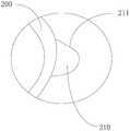
如图3所示,图3示出的是图1中K处的第二实施例的局部放大图。本发明实施例中相邻的两个密封环200的其中一个密封环200包括多个指状部210,指状部210朝向另一个密封环200的方向延伸,且不与另一个密封环200连接。As shown in FIG. 3 , FIG. 3 shows a partial enlarged view of the second embodiment at K in FIG. 1 . In the embodiment of the present invention, one of the two adjacent sealing rings 200 includes a plurality of
一个密封环200上的多个指状部210可以与波峰部220的数量相同,多个指状部210可以分别设置在多个波峰部220的顶点处。通过指状部210的设计,可进一步增大密封环200的拦截面积,有助于提高密封环200的防护效果。The number of the plurality of
当然,可以理解的是,上述的多个指状部210可以不设置在多个波峰部220的顶点处,而是设置在波峰部220的其他区域;亦或是,多个指状部210分别设置在多个波谷部230的底点处;再或是,多个指状部210设置在多个波谷部230的除了底点处的其他区域。Of course, it can be understood that the above-mentioned plurality of
如图4所示,图4示出的是图3中L处的指状部210的一实施方式的局部放大图。本发明实施例的指状部210具有弧形表面211,弧形表面211朝向另一个密封环200。由于弧形表面211相对于平面的表面积更大,更进一步增大了密封环200的拦截面积,进一步提高了密封环200的防护效果。As shown in FIG. 4 , FIG. 4 shows a partial enlarged view of an embodiment of the
当然,在其他实施方式中,指状部210还可以具有其他形状的表面。Of course, in other embodiments, the
如图5所示,图5示出的是图1中K处的第三实施例的局部放大图。本发明实施例的相邻的两个密封环200之间通过多个指状部210相连接。相邻的两个密封环200之间的多个指状部210围绕集成电路区域110的周边相间隔设置。As shown in FIG. 5 , FIG. 5 shows a partial enlarged view of the third embodiment at K in FIG. 1 . In the embodiment of the present invention, two adjacent sealing rings 200 are connected by a plurality of
通过多个指状部210连接于相邻的两个密封环200的设计,使得多个密封环200之间并非独立设置,而是形成一网状结构,网状结构的密封环200更加坚固,其防护作用更强。Through the design that the plurality of
如图6所示,图6示出的是图1中K处的第四实施例的局部放大图。本发明实施例的相邻的两个密封环200的其中一个密封环200的多个波峰部220与另一个密封环200的多个波谷部230对应设置。相邻的两个密封环200的其中一个密封环200的多个波谷部230与另一个密封环200的多个波峰部220对应设置。As shown in FIG. 6 , FIG. 6 shows a partial enlarged view of the fourth embodiment at K in FIG. 1 . In the embodiment of the present invention, the plurality of
这样,在沿着垂直于多个密封环200的截面上,波峰部220和波谷部230是交替设置的,当裂纹向集成电路区域110内部传播时,由于波峰部220的凸面和波谷部230的凹面交替设置,其中一个密封环200的波峰部220与另一个密封环200的波谷部230之间的空间201变大更大。裂纹向内传播时,需依次穿过波峰部220/空间201/波谷部230/波峰部220/空间201等,这种结构的设计,更加有助于防止裂纹、离子或湿气向内传播。In this way, on a cross section perpendicular to the plurality of sealing
当然,可以理解的是,上述相邻的两个密封环200还可以采取除了上述波峰部220与波谷部230对应设置的方式相错设置,例如其中一个密封环200和与之相邻的另一个密封环200上下错开一定距离。Of course, it can be understood that the above-mentioned two adjacent sealing rings 200 can also be arranged in a staggered manner in addition to the above-mentioned corresponding arrangement of the
另外,还可以理解的是,图6所示的实施例还可以设有多个指状部210,指状部210可以自一个密封环200向另一个密封环200延伸,而不与该另一个密封环200相连接;也可以是,指状部210与相邻的两个密封环200相连接。关于指状部210的结构和优点与上述图4和图6所示实施例相同,此处不再赘述。In addition, it can also be understood that the embodiment shown in FIG. 6 may also be provided with a plurality of
下面结合图7至图13,详细说明本发明实施例的半导体装置的制作方法。图7至13示出的是本发明实施例的半导体装置的制作方法的不同工艺阶段的剖视图,其中图7至11示出的是图2中沿A-A的剖视图,图12和图13示出的是图5中沿B-B的剖视图。The fabrication method of the semiconductor device according to the embodiment of the present invention will be described in detail below with reference to FIG. 7 to FIG. 13 . FIGS. 7 to 13 are cross-sectional views of different process stages of a method for fabricating a semiconductor device according to an embodiment of the present invention, wherein FIGS. 7 to 11 are cross-sectional views along A-A in FIG. 2 , and FIGS. It is a sectional view taken along B-B in FIG. 5 .
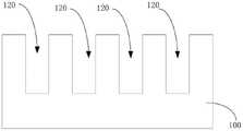
如图7所示,提供一具有集成电路区域110的半导体基底100,在半导体基底100上形成一个或多个沟槽120,沟槽120围绕集成电路区域110的周边布置。As shown in FIG. 7 , a
在一实施方式中,半导体基底100可以包含半导体材料如基体硅或单晶硅。在其他实施例或额外实施例中,半导体基底100中可包含另一半导体元素如结晶结构的锗。半导体基底100亦可包含半导体化合物如硅锗、碳化硅、砷化镓、磷化镓、磷化铟、砷化铟、锑化铟、或上述的组合。半导体基底100亦可包含绝缘层上半导体基底100如绝缘层上硅基底、绝缘层上硅锗基底、或绝缘层上锗基底。In one embodiment, the
在一些实施例中,半导体基底100为块材(bulk)半导体基底,例如半导体晶片。举例而言,半导体基底100包含硅或其他元素半导体材料,例如锗。半导体基底100可经掺杂(例如P型、N型或前述的组合)或不经掺杂。在一些实施例中,半导体基底100包含介电层上外延成长的半导体层。外延成长的半导体层可由硅锗、硅、锗、一或多个其他合适的材料或前述的组合制成。In some embodiments, the
在一些其他的实施例中,半导体基底100包含化合物半导体。举例而言,化合物半导体包含一或多个III-V族化合物半导体,具有由式AlX1GaX2InX3AsY1PY2NY3SbY4定义的组成,其中X1、X2、X3、Y1、Y2、Y3和Y4代表相对的比例。它们各自大于或等于0,且整体相加等于1。化合物半导体可包含碳化硅、砷化镓、砷化铟、磷化铟、一或多个其他合适的化合物半导体或前述的组合。也可使用其他包含II-VI族化合物半导体的合适的基底。In some other embodiments, the
在一些实施例中,半导体基底100为绝缘体上覆半导体(semiconductor-on-insulator,SOI)基底的主动层。绝缘体上覆半导体基底的制造可使用注入氧隔离(separation by implantation of oxygen,SIMOX)工艺、晶片接合工艺、其他合适的工艺或前述的组合。在一些其他的实施例中,半导体基底100包含多层结构。举例而言,半导体基底100包含形成在块材硅层上的硅锗层。In some embodiments, the
形成一个或多个沟槽120的方法,可以在半导体基底100上沉积一掩模层300,该掩模层300界定出该一个或多个沟槽120。在一实施方式中,掩模层300可以为光刻胶。The method of forming one or
如图8所示,在半导体基底100上沉积一掩模层300后,进行蚀刻,以形成上述的沟槽120。在一实施方式中,蚀刻可采用任何现在已知或以后开发的适用于移除材料的技术,其包含但不限于:干式蚀刻工艺(例如:电浆蚀刻、无电浆气体蚀刻、溅射蚀刻(sputteretching)、离子铣磨(ion milling)、反应离子蚀刻(reactive ion etching,RIE);或者湿式蚀刻工艺(例如:施用酸、碱、或溶剂来溶解结构的一部分、或使用研磨剂配方来研磨掉结构的一部分)。As shown in FIG. 8 , after depositing a
如图9所示,形成沟槽120后,在沟槽120表面形成一与所述沟槽120表面共形的阻挡层400。在一实施方式中,阻挡层400的形成可使用化学气相沉积工艺、原子层沉积工艺、物理气相沉积工艺、电浆辅助化学气相沉积工艺、电镀工艺、无电电镀工艺、旋转涂布工艺、一或多个其他合适的工艺或前述的组合。As shown in FIG. 9 , after the
在一实施方式中,阻挡层400可以包括氮化钛(TiN)或其他合适的材料。In one embodiment, the
如图10所示,形成阻挡层400后,在所述阻挡层400的上方形成一金属层500。在一实施方式中,金属层500可以包括钨或铝。As shown in FIG. 10 , after the
在一实施方式中,金属层500的形成可使用化学气相沉积工艺、原子层沉积工艺、物理气相沉积工艺、电浆辅助化学气相沉积工艺、电镀工艺、无电电镀工艺、旋转涂布工艺、一或多个其他合适的工艺或前述的组合。In one embodiment, the
如图11所示,金属层500形成后,去除部分金属层500和部分阻挡层400,以形成密封环200。在一实施方式中,去除部分金属层500和部分阻挡层400可采用化学机械研磨工艺、磨削工艺、蚀刻工艺、干式研磨工艺、湿法清洗、一或多个其他合适的工艺或前述的组合。As shown in FIG. 11 , after the
如图12和图13所示,图12和图13示出的是图5中沿B-B的剖视图。其中,图12示出的是在半导体基底100上形成沟槽120后,依次形成阻挡层400和金属层500。图13示出的是去除部分阻挡层400和金属层500后,形成密封环200。由于该B-B处相邻的两个密封环200是通过指状部210相连接,故在阻挡层400上形成的金属层500仅示出两个密封环200,且相比图11中的密封环200的宽度更宽。As shown in FIG. 12 and FIG. 13 , FIG. 12 and FIG. 13 show a cross-sectional view along B-B in FIG. 5 . 12 shows that after the
综上所述,本发明实施例的半导体装置及其制作方法的优点和有益效果在于:To sum up, the advantages and beneficial effects of the semiconductor device and the fabrication method thereof according to the embodiments of the present invention are as follows:
本发明实施例的密封环200具有波浪形结构,该波浪形结构使密封环200朝向集成电路区域110方向的表面以及背离集成电路区域110的方向的表面均呈弧形表面,弧形表面相比平面具有更大的拦截面积,使本发明实施例的密封环200能够更加有效地防止湿气和离子进入集成电路区域110内以及防止裂缝朝向集成电路区域110内传播,显著提高了密封环200的防护作用。The sealing
在此应注意,附图中示出而且在本说明书中描述的半导体装置及其制作方法仅仅是采用本发明的原理的一个示例。本领域的普通技术人员应当清楚地理解,本发明的原理并非仅限于附图中示出或说明书中描述的装置的任何细节或任何部件。It should be noted here that the semiconductor device and method of fabricating the same shown in the accompanying drawings and described in this specification are but one example to which the principles of the present invention are employed. It should be clearly understood by those skilled in the art that the principles of the invention are not limited to any detail or any component of the apparatus illustrated in the drawings or described in the specification.
应可理解的是,本发明不将其应用限制到本说明书提出的部件的详细结构和布置方式。本发明能够具有其他实施方式,并且能够以多种方式实现并且执行。前述变形形式和修改形式落在本发明的范围内。应可理解的是,本说明书公开和限定的本发明延伸到文中和/或附图中提到或明显的两个或两个以上单独特征的所有可替代组合。所有这些不同的组合构成本发明的多个可替代方面。本说明书所述的实施方式说明了已知用于实现本发明的最佳方式,并且将使本领域技术人员能够利用本发明。It should be understood that the present invention is not limited in its application to the detailed structure and arrangement of components set forth in this specification. The invention is capable of other embodiments, of being implemented and of being carried out in various ways. The aforementioned variations and modifications fall within the scope of the present invention. It will be understood that the invention disclosed and defined in this specification extends to all alternative combinations of two or more of the individual features mentioned or evident in the text and/or drawings. All of these different combinations constitute various alternative aspects of the present invention. The embodiments described in this specification illustrate the best mode known for carrying out the invention, and will enable any person skilled in the art to utilize the invention.
Claims (12)
Translated fromChinesePriority Applications (3)
| Application Number | Priority Date | Filing Date | Title |
|---|---|---|---|
| CN202011170771.7ACN114512447B (en) | 2020-10-28 | 2020-10-28 | Semiconductor device and method for manufacturing the same |
| PCT/CN2021/104759WO2022088745A1 (en) | 2020-10-28 | 2021-07-06 | Semiconductor device and fabrication method therefor |
| US17/455,972US12132012B2 (en) | 2020-10-28 | 2021-11-22 | Semiconductor device and manufacturing method thereof |
Applications Claiming Priority (1)
| Application Number | Priority Date | Filing Date | Title |
|---|---|---|---|
| CN202011170771.7ACN114512447B (en) | 2020-10-28 | 2020-10-28 | Semiconductor device and method for manufacturing the same |
Publications (2)
| Publication Number | Publication Date |
|---|---|
| CN114512447Atrue CN114512447A (en) | 2022-05-17 |
| CN114512447B CN114512447B (en) | 2025-02-21 |
Family
ID=81381857
Family Applications (1)
| Application Number | Title | Priority Date | Filing Date |
|---|---|---|---|
| CN202011170771.7AActiveCN114512447B (en) | 2020-10-28 | 2020-10-28 | Semiconductor device and method for manufacturing the same |
Country Status (2)
| Country | Link |
|---|---|
| CN (1) | CN114512447B (en) |
| WO (1) | WO2022088745A1 (en) |
Citations (6)
| Publication number | Priority date | Publication date | Assignee | Title |
|---|---|---|---|---|
| JPH07201855A (en)* | 1993-12-28 | 1995-08-04 | Fujitsu Ltd | Semiconductor device |
| US20020167071A1 (en)* | 2001-05-10 | 2002-11-14 | Mu-Chun Wang | Guard ring for protecting integrated circuits |
| CN1610092A (en)* | 2003-10-23 | 2005-04-27 | 株式会社瑞萨科技 | Semiconductor device |
| CN105702636A (en)* | 2014-12-16 | 2016-06-22 | 三星电子株式会社 | Moisture blocking structure and/or a guard ring, a semiconductor device, and a manufacturing method |
| TWI686905B (en)* | 2019-02-18 | 2020-03-01 | 世界先進積體電路股份有限公司 | Semiconductor structure |
| CN110875256A (en)* | 2018-08-30 | 2020-03-10 | 南亚科技股份有限公司 | Semiconductor element and method for manufacturing the same |
Family Cites Families (4)
| Publication number | Priority date | Publication date | Assignee | Title |
|---|---|---|---|---|
| US6492716B1 (en)* | 2001-04-30 | 2002-12-10 | Zeevo, Inc. | Seal ring structure for IC containing integrated digital/RF/analog circuits and functions |
| JP4636839B2 (en)* | 2004-09-24 | 2011-02-23 | パナソニック株式会社 | Electronic devices |
| CN102315247B (en)* | 2010-07-08 | 2013-04-24 | 上海华虹Nec电子有限公司 | Super-junction semiconductor device with groove-type terminal structure |
| US10128201B2 (en)* | 2017-02-16 | 2018-11-13 | Globalfoundries Singapore Pte. Ltd. | Seal ring for wafer level package |
- 2020
- 2020-10-28CNCN202011170771.7Apatent/CN114512447B/enactiveActive
- 2021
- 2021-07-06WOPCT/CN2021/104759patent/WO2022088745A1/ennot_activeCeased
Patent Citations (6)
| Publication number | Priority date | Publication date | Assignee | Title |
|---|---|---|---|---|
| JPH07201855A (en)* | 1993-12-28 | 1995-08-04 | Fujitsu Ltd | Semiconductor device |
| US20020167071A1 (en)* | 2001-05-10 | 2002-11-14 | Mu-Chun Wang | Guard ring for protecting integrated circuits |
| CN1610092A (en)* | 2003-10-23 | 2005-04-27 | 株式会社瑞萨科技 | Semiconductor device |
| CN105702636A (en)* | 2014-12-16 | 2016-06-22 | 三星电子株式会社 | Moisture blocking structure and/or a guard ring, a semiconductor device, and a manufacturing method |
| CN110875256A (en)* | 2018-08-30 | 2020-03-10 | 南亚科技股份有限公司 | Semiconductor element and method for manufacturing the same |
| TWI686905B (en)* | 2019-02-18 | 2020-03-01 | 世界先進積體電路股份有限公司 | Semiconductor structure |
Also Published As
| Publication number | Publication date |
|---|---|
| WO2022088745A1 (en) | 2022-05-05 |
| CN114512447B (en) | 2025-02-21 |
Similar Documents
| Publication | Publication Date | Title |
|---|---|---|
| US12324247B2 (en) | Integrated standard cell structure | |
| CN103378155B (en) | Pseudo-FinFET structure and manufacture method thereof | |
| CN102290378B (en) | Semiconductor device and method for manufacturing the same | |
| KR101645820B1 (en) | Finfet seal ring | |
| CN109980012A (en) | Semiconductor devices | |
| US8747992B2 (en) | Non-uniform semiconductor device active area pattern formation | |
| CN112530943A (en) | Semiconductor device and method for manufacturing the same | |
| CN106876336A (en) | Semiconductor structure and its manufacture method | |
| TWI775766B (en) | Semiconductor devices | |
| US9048246B2 (en) | Die seal ring and method of forming the same | |
| TW202011607A (en) | Semiconductor device and manufacturing method thereof | |
| CN111969044A (en) | Semiconductor device with a plurality of semiconductor chips | |
| KR102785033B1 (en) | Semiconductor device and manufacturing method | |
| WO2021065590A1 (en) | Semiconductor integrated circuit device and method of manufacturing semiconductor integrated circuit device | |
| CN114512447B (en) | Semiconductor device and method for manufacturing the same | |
| CN108122839B (en) | Method of manufacturing semiconductor device | |
| US12132012B2 (en) | Semiconductor device and manufacturing method thereof | |
| US12040237B2 (en) | Semiconductor device structure with spacer | |
| TWI723062B (en) | Semiconductor device structure and method for forming the same | |
| US12205849B2 (en) | Semiconductor device structure with source/drain structure and method for forming the same | |
| CN113053828B (en) | Sealing ring and forming method thereof | |
| US20230387117A1 (en) | Semiconductor device structure with air gap and method for forming the same | |
| US20240105775A1 (en) | Semiconductor device structure and method for forming the same | |
| TW202517062A (en) | Method of manufacturing semiconductor structure | |
| CN118888572A (en) | Semiconductor structure and method for manufacturing the same |
Legal Events
| Date | Code | Title | Description |
|---|---|---|---|
| PB01 | Publication | ||
| PB01 | Publication | ||
| SE01 | Entry into force of request for substantive examination | ||
| SE01 | Entry into force of request for substantive examination | ||
| GR01 | Patent grant | ||
| GR01 | Patent grant |