CN114499484B - Dual-band ultra-wideband 4 x 8 radio frequency matrix switch - Google Patents
Dual-band ultra-wideband 4 x 8 radio frequency matrix switchDownload PDFInfo
- Publication number
- CN114499484B CN114499484BCN202111623787.3ACN202111623787ACN114499484BCN 114499484 BCN114499484 BCN 114499484BCN 202111623787 ACN202111623787 ACN 202111623787ACN 114499484 BCN114499484 BCN 114499484B
- Authority
- CN
- China
- Prior art keywords
- transistor
- drain
- source
- radio frequency
- gate
- Prior art date
- Legal status (The legal status is an assumption and is not a legal conclusion. Google has not performed a legal analysis and makes no representation as to the accuracy of the status listed.)
- Active
Links
Images
Classifications
- H—ELECTRICITY
- H03—ELECTRONIC CIRCUITRY
- H03K—PULSE TECHNIQUE
- H03K17/00—Electronic switching or gating, i.e. not by contact-making and –breaking
- H03K17/51—Electronic switching or gating, i.e. not by contact-making and –breaking characterised by the components used
- H03K17/56—Electronic switching or gating, i.e. not by contact-making and –breaking characterised by the components used by the use, as active elements, of semiconductor devices
- H03K17/687—Electronic switching or gating, i.e. not by contact-making and –breaking characterised by the components used by the use, as active elements, of semiconductor devices the devices being field-effect transistors
- H03K17/693—Switching arrangements with several input- or output-terminals, e.g. multiplexers, distributors
- H—ELECTRICITY
- H03—ELECTRONIC CIRCUITRY
- H03K—PULSE TECHNIQUE
- H03K17/00—Electronic switching or gating, i.e. not by contact-making and –breaking
- H03K17/51—Electronic switching or gating, i.e. not by contact-making and –breaking characterised by the components used
- H03K17/56—Electronic switching or gating, i.e. not by contact-making and –breaking characterised by the components used by the use, as active elements, of semiconductor devices
- H03K17/687—Electronic switching or gating, i.e. not by contact-making and –breaking characterised by the components used by the use, as active elements, of semiconductor devices the devices being field-effect transistors
- H03K17/6871—Electronic switching or gating, i.e. not by contact-making and –breaking characterised by the components used by the use, as active elements, of semiconductor devices the devices being field-effect transistors the output circuit comprising more than one controlled field-effect transistor
- Y—GENERAL TAGGING OF NEW TECHNOLOGICAL DEVELOPMENTS; GENERAL TAGGING OF CROSS-SECTIONAL TECHNOLOGIES SPANNING OVER SEVERAL SECTIONS OF THE IPC; TECHNICAL SUBJECTS COVERED BY FORMER USPC CROSS-REFERENCE ART COLLECTIONS [XRACs] AND DIGESTS
- Y02—TECHNOLOGIES OR APPLICATIONS FOR MITIGATION OR ADAPTATION AGAINST CLIMATE CHANGE
- Y02D—CLIMATE CHANGE MITIGATION TECHNOLOGIES IN INFORMATION AND COMMUNICATION TECHNOLOGIES [ICT], I.E. INFORMATION AND COMMUNICATION TECHNOLOGIES AIMING AT THE REDUCTION OF THEIR OWN ENERGY USE
- Y02D30/00—Reducing energy consumption in communication networks
- Y02D30/70—Reducing energy consumption in communication networks in wireless communication networks
Landscapes
- Electronic Switches (AREA)
Abstract
Translated fromChinese
Description
Translated fromChinese技术领域technical field
本发明属于射频集成电路技术领域,具体涉及一种双频段超宽带4×8射频矩阵开关。The invention belongs to the technical field of radio frequency integrated circuits, and in particular relates to a dual-
背景技术Background technique
在如今的无线通信时代,随着射频集成电路和电子信息产业的发展,无线通信终端集成度越来越高,通信技术的标准也更加丰富,通信频段拥挤、通信模式并存,针对单一频段的射频接收前端已逐渐不能满足日常需求。为满足多频段通信需求,可重构射频前端应运而生。In today's wireless communication era, with the development of radio frequency integrated circuits and electronic information industry, the integration of wireless communication terminals is getting higher and higher, the standards of communication technology are also more abundant, the communication frequency bands are crowded, and the communication modes coexist. The receiving front end has gradually failed to meet daily needs. In order to meet the needs of multi-band communication, a reconfigurable RF front-end emerges as the times require.
射频矩阵开关是可重构射频前端的关键模块,通过射频矩阵开关对射频前端模块(如低噪声放大器、滤波器)进行切换实现射频前端的重构来满足不同频段的通信需求。射频矩阵开关含有多个输入端和多个输出端,因此可以将任何一个输入连接到任何一个输出。射频矩阵开关分为阻塞矩阵、非阻塞矩阵和完整或部分访问矩阵。阻塞矩阵允许将单个输入连接到任何单个输出,因此,在任何给定时间只有一个信号路径是可用的。常见的阻塞型矩阵开关采用两个单刀多掷开关背对背相连,即单刀端与单刀端相连。这种开关结构简单,但由于开关支路多,高频信号会从关断支路泄露,导致隔离度低,插损大。非阻塞矩阵允许同时连接多个输入/输出信号路径。常见的非阻塞矩阵开关由多个横向单刀多掷开关和纵向单刀多掷开关构成,横向每个单刀多掷开关的每一个掷分别与每个纵向的单刀多掷开关的一个掷相连,例如,若要构成4×4矩阵开关,则需要4个横向单刀四掷开关和4个纵向单刀四掷开关,每个横向单刀四掷开关的4个掷分别连接4个不同纵向单刀四掷开关的一个掷。非阻塞矩阵的电路结构复杂,面积较大,同时也由于开关支路多,高频信号从关断支路泄露,导致隔离度低,插损大等问题。完整或部分访问矩阵的常见结构是采用多个多路功分器和多个单刀多掷开关的形式,例如若要构成4×4矩阵开关,则需要4个四路功分器和4个单刀四掷开关,每个四路功分器的一路连接一个单刀四掷开关的一个掷,由此实现将一个输入通过功分器连接到多个输出端口。该种结构同样面临电路复杂,面积大,成本较高等问题,另外,由于引入功分器,将输入信号分成多路输出,导致插损很大,如四路功分器便会引入4dB的插损,同时由于功分器的带宽有限,矩阵开关难以做到宽频带。The RF matrix switch is a key module of the reconfigurable RF front-end. The RF front-end modules (such as low-noise amplifiers and filters) are switched through the RF matrix switch to realize the reconfiguration of the RF front-end to meet the communication requirements of different frequency bands. RF matrix switches have multiple inputs and multiple outputs so that any input can be connected to any output. RF matrix switches are divided into blocking matrix, non-blocking matrix and full or partial access matrix. A blocking matrix allows a single input to be connected to any single output, so only one signal path is available at any given time. A common blocking matrix switch uses two single-pole multi-throw switches connected back to back, that is, the single-pole end is connected to the single-pole end. This kind of switch has a simple structure, but because there are many switching branches, high-frequency signals will leak from the off branch, resulting in low isolation and large insertion loss. A non-blocking matrix allows multiple input/output signal paths to be connected simultaneously. A common non-blocking matrix switch is composed of multiple horizontal SPMT switches and vertical SPMT switches. Each throw of each horizontal SPMT switch is connected to a throw of each vertical SPMT switch. For example, To form a 4×4 matrix switch, you need 4 horizontal SP4T switches and 4 vertical SP4T switches, and the 4 throws of each horizontal SP4T switch are connected to one of 4 different vertical SP4T switches toss. The circuit structure of the non-blocking matrix is complex and the area is large. At the same time, due to the large number of switching branches, the high-frequency signal leaks from the off branch, resulting in low isolation and large insertion loss. A common structure for a full or partial access matrix is in the form of multiple multi-channel power dividers and multiple single-pole multi-throw switches. For example, to form a 4×4 matrix switch, four four-way power dividers and four single-pole For a four-throw switch, one side of each four-way power divider is connected to one throw of a single-pole four-throw switch, thereby realizing the connection of one input to multiple output ports through the power divider. This structure also faces the problems of complex circuit, large area, and high cost. In addition, due to the introduction of a power divider, the input signal is divided into multiple outputs, resulting in a large insertion loss. For example, a four-way power divider will introduce a 4dB insertion loss. At the same time, due to the limited bandwidth of the power divider, it is difficult for the matrix switch to achieve a wide frequency band.
因此如何实现可以覆盖多个通信协议频段的超宽带射频矩阵开关的设计,且使射频矩阵开关具有结构简单、低成本、低损耗的优势,就成为了研究热点。Therefore, how to realize the design of an ultra-wideband RF matrix switch that can cover multiple communication protocol frequency bands, and how to make the RF matrix switch have the advantages of simple structure, low cost, and low loss has become a research hotspot.
发明内容Contents of the invention
针对背景技术所存在的问题,本发明的目的在于提供一种双频段超宽带4×8射频矩阵开关。该矩阵开关包括三个单刀四掷射频开关(SP4T)和一个开关滤波电路构成,通过开关的切换,使得开关滤波电路一条输出支路呈现高通滤波或低通滤波,而另一条输出支路呈现关闭状态,即使得矩阵开关有两种模式,高频输出模式或低频输出模式;同时,在任意模式工作时,滤波电路的存在使得射频信号很难从关闭的支路泄露出去,从而降低了矩阵开关的插入损耗。In view of the problems existing in the background technology, the object of the present invention is to provide a dual-
为实现上述目的,本发明的技术方案如下:To achieve the above object, the technical scheme of the present invention is as follows:
一种双频段超宽带4×8射频矩阵开关,包括控制网络、一个输入单刀四掷射频开关、两个输出单刀四掷射频开关(SP4T)和一个开关滤波电路;其中,输入单刀四掷射频开关的单刀端与开关滤波电路的输入端相连;两个输出单刀四掷射频开关的单刀端分别与开关滤波电路的两个输出端相连;A dual-
所述开关滤波电路包括高通滤波和低通滤波两条支路,两条支路共用同一个输入端,其中,高通滤波支路由一个电容和一个晶体管串联组成,低通滤波支路包括一个电感和两个晶体管,其中一个晶体管串联在支路上,另一个晶体管并联在支路上;The switching filter circuit includes two branches of high-pass filtering and low-pass filtering, and the two branches share the same input terminal, wherein the high-pass filtering branch is composed of a capacitor and a transistor in series, and the low-pass filtering branch includes an inductor and Two transistors, one of which is connected in series on the branch, and the other transistor is connected in parallel on the branch;
输入单刀四掷射频开关的四个掷为射频矩阵开关的四个输入端,两个输出单刀四掷射频开关的掷为射频矩阵开关的八个输出端;The four throws of the input single-pole four-throw radio frequency switch are the four input terminals of the radio frequency matrix switch, and the throws of the two output single-pole four-throw radio frequency switches are the eight output terminals of the radio frequency matrix switch;
所述控制网络用于为射频矩阵开关中的晶体管提供偏置电压。The control network is used to provide bias voltage for transistors in the radio frequency matrix switch.
进一步地,所述两个输出单刀四掷射频开关分别为高频段单刀四掷射频开关和低频段单刀四掷射频开关;高频段单刀四掷射频开关与低频端单刀四掷射频开关的拓扑结构一致,低频端单刀四掷射频开关的晶体管尺寸较高频段单刀四掷射频开关的晶体管尺寸更大。这是因为低频段单刀四掷射频开关的插损主要由晶体管的寄生电阻决定,晶体管尺寸越大,晶体管导通时的等效电阻越小,而高频段单刀四掷射频开关的插损主要由于信号从关断支路的关断晶体管泄露,处于关断态下的晶体管等效为寄生电容,晶体管尺寸越小,寄生电容越小,信号泄露也越小;Further, the two output single-pole four-throw radio frequency switches are respectively a high-frequency single-pole four-throw radio frequency switch and a low-frequency single-pole four-throw radio frequency switch; the topology of the high-frequency single-pole four-throw radio frequency switch is consistent with that of the low-frequency end single-pole four-throw radio frequency switch , the transistor size of the low-frequency end single-pole four-throw RF switch is larger than that of the high-frequency end single-pole four-throw RF switch. This is because the insertion loss of the low-frequency single-pole four-throw RF switch is mainly determined by the parasitic resistance of the transistor. The larger the transistor size, the smaller the equivalent resistance when the transistor is turned on, while the insertion loss of the high-frequency single-pole four-throw RF switch is mainly due to The signal leaks from the turn-off transistor of the turn-off branch, and the transistor in the turn-off state is equivalent to a parasitic capacitance. The smaller the transistor size, the smaller the parasitic capacitance, and the smaller the signal leakage;
进一步地,高频段单刀四掷射频开关与开关滤波电路的高通滤波支路相连,低频段单刀四掷射频开关与开关滤波电路的低通滤波支路相连;即低频段单刀四掷射频开关的输出端口当作矩阵开关的低频段输出端口,高频段单刀四掷射频开关的输出端口当作矩阵开关的高频段输出端口。Further, the high-frequency single-pole four-throw radio frequency switch is connected to the high-pass filter branch of the switch filter circuit, and the low-frequency single-pole four-throw radio frequency switch is connected to the low-pass filter branch of the switch filter circuit; that is, the output of the low-frequency single-pole four-throw radio frequency switch The port is used as the low-frequency output port of the matrix switch, and the output port of the high-frequency single-pole four-throw RF switch is used as the high-frequency output port of the matrix switch.
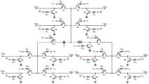
进一步地,所述控制网络包括偏置电阻Rg1-Rg25;所述输入单刀四掷射频开关包括晶体管M1-M8;所述开关滤波电路包括晶体管M25、M26、M27,及第一电容C1、第一电感L1;高频段单刀四掷射频开关包括晶体管M9-M16;低频段单刀四掷射频开关包括晶体管M17-M24;Further, the control network includes bias resistors Rg1-Rg25; the input single-pole four-throw radio frequency switch includes transistors M1-M8; the switch filter circuit includes transistors M25, M26, M27, and a first capacitor C1, a first Inductor L1; high-frequency single-pole four-throw RF switch includes transistors M9-M16; low-frequency single-pole four-throw RF switch includes transistors M17-M24;
其中,第一输入端口Port1与晶体管M1的源极、晶体管M2的漏极相连,晶体管M2的栅极与偏置电阻Rg3相连,晶体管M2的源极接地,晶体管M1的栅极与偏置电阻Rg1一端相连,晶体管M1的漏极与晶体管M3的漏极、晶体管M5的漏极、晶体管M7的漏极、电容C1的一端、电感L1的一端相连,晶体管M3的源极与晶体管M4的漏极、第二输入端口Port2相连,晶体管M3的栅极与偏置电阻Rg2的一端相连,晶体管M4的源极接地,晶体管M4的栅极与偏置电阻Rg4一端相连,晶体管M5的源极与晶体管M6的漏极、第三输入端口Port3相连,晶体管M5的栅极与偏置电阻Rg5的一端相连,晶体管M6的源极接地,晶体管M6的栅极与偏置电阻Rg7一端相连,晶体管M7的源极与晶体管M8的漏极、第四输入端口Port4相连,晶体管M7的栅极与偏置电阻Rg6的一端相连,晶体管M8的源极接地,晶体管M8的栅极与偏置电阻Rg8一端相连,电容C1的另一端与晶体管M25的漏极相连,晶体管M25的栅极与偏置电阻Rg25的一端相连,电感L1的另一端与晶体管M27的漏极、晶体管M26的源极相连,晶体管M27的栅极与偏置电阻Rg27的一端相连,晶体管M26的栅极与偏置电阻Rg26的一端相连,输出端口Port5与晶体管M9的源极、晶体管M10的漏极相连,晶体管M10的栅极与偏置电阻Rg11相连,晶体管M10的源极接地,晶体管M9的栅极与偏置电阻Rg9一端相连,晶体管M9的漏极与晶体管M11的漏极、晶体管M13的漏极、晶体管M15的漏极、晶体管M25的源极相连,晶体管M11的源极与晶体管M12的漏极、输出端口Port6相连,晶体管M11的栅极与偏置电阻Rg10的一端相连,晶体管M12的源极接地,晶体管M12的栅极与偏置电阻Rg12一端相连,晶体管M13的源极与晶体管M14的漏极、输出端口Port7相连,晶体管M13的栅极与偏置电阻Rg13的一端相连,晶体管M14的源极接地,晶体管M14的栅极与偏置电阻Rg15一端相连,晶体管M15的源极与晶体管M16的漏极、输出端口Port8相连,晶体管M15的栅极与偏置电阻Rg14的一端相连,晶体管M16的源极接地,晶体管M16的栅极与偏置电阻Rg16一端相连,输出端口Port9与晶体管M17的源极、晶体管M18的漏极相连,晶体管M18的栅极与偏置电阻Rg19相连,晶体管M18的源极接地,晶体管M17的栅极与偏置电阻Rg17一端相连,晶体管M17的漏极与晶体管M19的漏极、晶体管M21的漏极、晶体管M23的漏极、晶体管M26的漏极相连,晶体管M19的源极与晶体管M20的漏极、输出端口Port10相连,晶体管M19的栅极与偏置电阻Rg18的一端相连,晶体管M20的源极接地,晶体管M20的栅极与偏置电阻Rg20一端相连,晶体管M21的源极与晶体管M22的漏极、输出端口Port11相连,晶体管M21的栅极与偏置电阻Rg21的一端相连,晶体管M22的源极接地,晶体管M22的栅极与偏置电阻Rg23一端相连,晶体管M23的源极与晶体管M24的漏极、输出端口Port12相连,晶体管M23的栅极与偏置电阻Rg22的一端相连,晶体管M24的源极接地,晶体管M24的栅极与偏置电阻Rg24一端相连。Wherein, the first input port Port1 is connected to the source of the transistor M1 and the drain of the transistor M2, the gate of the transistor M2 is connected to the bias resistor Rg3, the source of the transistor M2 is grounded, and the gate of the transistor M1 is connected to the bias resistor Rg1 One end is connected, the drain of the transistor M1 is connected with the drain of the transistor M3, the drain of the transistor M5, the drain of the transistor M7, one end of the capacitor C1, and one end of the inductor L1, and the source of the transistor M3 is connected with the drain of the transistor M4, The second input port Port2 is connected, the gate of the transistor M3 is connected to one end of the bias resistor Rg2, the source of the transistor M4 is grounded, the gate of the transistor M4 is connected to one end of the bias resistor Rg4, the source of the transistor M5 is connected to the end of the transistor M6 The drain is connected to the third input port Port3, the gate of the transistor M5 is connected to one end of the bias resistor Rg5, the source of the transistor M6 is grounded, the gate of the transistor M6 is connected to one end of the bias resistor Rg7, and the source of the transistor M7 is connected to one end of the bias resistor Rg7. The drain of the transistor M8 is connected to the fourth input port Port4, the gate of the transistor M7 is connected to one end of the bias resistor Rg6, the source of the transistor M8 is grounded, the gate of the transistor M8 is connected to one end of the bias resistor Rg8, and the capacitor C1 The other end is connected to the drain of the transistor M25, the gate of the transistor M25 is connected to one end of the bias resistor Rg25, the other end of the inductor L1 is connected to the drain of the transistor M27 and the source of the transistor M26, and the gate of the transistor M27 is connected to the bias resistor Rg25. One end of the setting resistor Rg27 is connected, the gate of the transistor M26 is connected to one end of the biasing resistor Rg26, the output port Port5 is connected to the source of the transistor M9 and the drain of the transistor M10, the gate of the transistor M10 is connected to the biasing resistor Rg11, The source of the transistor M10 is grounded, the gate of the transistor M9 is connected to one end of the bias resistor Rg9, the drain of the transistor M9 is connected to the drain of the transistor M11, the drain of the transistor M13, the drain of the transistor M15, and the source of the transistor M25 , the source of the transistor M11 is connected to the drain of the transistor M12 and the output port Port6, the gate of the transistor M11 is connected to one end of the bias resistor Rg10, the source of the transistor M12 is grounded, and the gate of the transistor M12 is connected to one end of the bias resistor Rg12 The source of the transistor M13 is connected to the drain of the transistor M14 and the output port Port7, the gate of the transistor M13 is connected to one end of the bias resistor Rg13, the source of the transistor M14 is grounded, and the gate of the transistor M14 is connected to the bias resistor Rg15 One terminal is connected, the source of the transistor M15 is connected to the drain of the transistor M16 and the output port Port8, the gate of the transistor M15 is connected to one end of the bias resistor Rg14, the source of the transistor M16 is grounded, and the gate of the transistor M16 is connected to the bias resistor Rg14 One end of Rg16 is connected, the output port Port9 is connected to the source of the transistor M17 and the drain of the transistor M18, the gate of the transistor M18 is connected to the bias resistor Rg19, the source of the transistor M18 is grounded, the gate of the transistor M17 is connected to the bias resistor Rg17 One end is connected, the drain of the transistor M17 is connected with the drain of the transistor M19, the drain of the transistor M21, the drain of the transistor M23, and the drain of the transistor M26, and the source of the transistor M19 is connected with the drain of the transistor M20 and the output port Port10 , the gate of the transistor M19 is connected to one end of the bias resistor Rg18, the source of the transistor M20 is grounded, the gate of the transistor M20 is connected to one end of the bias resistor Rg20, the source of the transistor M21 is connected to the drain of the transistor M22, and the output port Port11 The gate of the transistor M21 is connected to one end of the bias resistor Rg21, the source of the transistor M22 is grounded, the gate of the transistor M22 is connected to one end of the bias resistor Rg23, the source of the transistor M23 is connected to the drain of the transistor M24, and the output port Port12 is connected, the gate of the transistor M23 is connected to one end of the bias resistor Rg22, the source of the transistor M24 is grounded, and the gate of the transistor M24 is connected to one end of the bias resistor Rg24.
综上所述,由于采用了上述技术方案,本发明的有益效果是:In summary, owing to adopting above-mentioned technical scheme, the beneficial effect of the present invention is:
本发明射频矩阵开关具有4个输入端口和8个输出端口,每个端口可以连接不同元器件,通过在不同元器件之间的切换实现射频前端的重构;且本发明射频矩阵开关在DC~18GHz频带内插损小于3.5dB,隔离度大于18dB,其中低频段输出端口在DC~9GHz内的插入损耗小于3.1dB,高频段输出端口在高频段8GHz~18GHz的插入损耗小于3.5dB;在低频段输出端导通时,高频段输出端到输入端的隔离度在DC~18GHz内大于18dB,在高频段输出端导通时,低频段输出端到输入端的隔离度在DC~18GHz内大于36dB。The radio frequency matrix switch of the present invention has 4 input ports and 8 output ports, and each port can be connected with different components, and the reconfiguration of the radio frequency front end is realized by switching between different components; and the radio frequency matrix switch of the present invention operates between DC~ The insertion loss in the 18GHz frequency band is less than 3.5dB, and the isolation is greater than 18dB. The insertion loss of the output port of the low frequency band is less than 3.1dB in the range of DC to 9GHz, and the insertion loss of the output port of the high frequency band is less than 3.5dB in the high frequency band of 8GHz to 18GHz; When the output end of the frequency band is turned on, the isolation from the output end of the high frequency band to the input end is greater than 18dB within DC to 18GHz.
附图说明Description of drawings
图1为本发明实施例1双频段超宽带4×8射频矩阵开关的电路结构图。FIG. 1 is a circuit structure diagram of a dual-
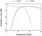
图2为本发明实施例1双频段超宽带4×8射频矩阵开关的插入损耗仿真图。FIG. 2 is a simulation diagram of insertion loss of a dual-
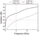
图3为本发明实施例1双频段超宽带4×8射频矩阵开关的隔离度仿真图。FIG. 3 is a simulation diagram of isolation of a dual-
具体实施方式Detailed ways
为使本发明的目的、技术方案和优点更加清楚,下面结合实施方式和附图,对本发明作进一步地详细描述。In order to make the purpose, technical solution and advantages of the present invention clearer, the present invention will be further described in detail below in conjunction with the implementation methods and accompanying drawings.
一种双频段超宽带4×8射频矩阵开关,包括控制网络,依次串联的输入SP4T、开关滤波电路,及与开关滤波电路两个输出端相连的高频段输出SP4T及低频段输出SP4T;A dual-
所述输入SP4T用于将四个输入端口的其中一个连接到开关滤波电路,并关闭其他输入端口;所述开关滤波电路用于切换高频段输出SP4T和低频段输出SP4T,开关滤波电路的一条输出支路串联电感作为低频支路,用于低通滤波,并在该支路关断时,减少高频信号流入,另一条支路串联电容作为高频支路,用于高通滤波,并在该支路关断时,减少低频信号流入,从而降低矩阵开关的插入损耗;所述高频段输出SP4T用于将开关滤波电路高频支路与一个输出端口相连,并关断其余端口;所述低频段输出SP4T用于将开关滤波电路低频支路与一个输出端口相连,并关断其余端口。The input SP4T is used to connect one of the four input ports to the switch filter circuit and close the other input ports; the switch filter circuit is used to switch the high-band output SP4T and the low-frequency output SP4T, and one output of the switch filter circuit The series inductor of the branch is used as a low-frequency branch for low-pass filtering, and when the branch is turned off, it reduces the inflow of high-frequency signals, and the other branch is used as a high-frequency branch for high-pass filtering. When the branch is turned off, the inflow of low-frequency signals is reduced, thereby reducing the insertion loss of the matrix switch; the high-frequency output SP4T is used to connect the high-frequency branch of the switch filter circuit to an output port, and turn off the remaining ports; the low-frequency The frequency band output SP4T is used to connect the low-frequency branch of the switch filter circuit with one output port and turn off the other ports.
实施例1Example 1
一种双频段超宽带4×8射频矩阵开关,其电路结构图如图1所示,包括控制网络、一个输入SP4T、两个输出SP4T和一个开关滤波电路;A dual-
输入SP4T包括晶体管M1、M2、M3、M4、M5、M6、M7、M8,所述晶体管M1的源极与输入端口Port1、晶体管M2的漏极相连,晶体管M2的栅极与偏置电阻Rg3相连,晶体管M2的源极接地,晶体管M1的栅极与偏置电阻Rg1一端相连,晶体管M1的漏极与晶体管M3的漏极、晶体管M5的漏极、晶体管M7的漏极、电容C1的一端、电感L1的一端相连,晶体管M3的源极与晶体管M4的漏极、输入端口Port2相连,晶体管M3的栅极与偏置电阻Rg2的一端相连,晶体管M4的源极接地,晶体管M4的栅极与偏置电阻Rg4一端相连,晶体管M5的源极与晶体管M6的漏极、输入端口Port3相连,晶体管M5的栅极与偏置电阻Rg5的一端相连,晶体管M6的源极接地,晶体管M6的栅极与偏置电阻Rg7一端相连,晶体管M7的源极与晶体管M8的漏极、输入端口Port4相连,晶体管M7的栅极与偏置电阻Rg6的一端相连,晶体管M8的源极接地,晶体管M8的栅极与偏置电阻Rg8一端相连;The input SP4T includes transistors M1, M2, M3, M4, M5, M6, M7, M8, the source of the transistor M1 is connected to the input port Port1 and the drain of the transistor M2, and the gate of the transistor M2 is connected to the bias resistor Rg3 , the source of the transistor M2 is grounded, the gate of the transistor M1 is connected to one end of the bias resistor Rg1, the drain of the transistor M1 is connected to the drain of the transistor M3, the drain of the transistor M5, the drain of the transistor M7, and one end of the capacitor C1, One end of the inductor L1 is connected, the source of the transistor M3 is connected to the drain of the transistor M4 and the input port Port2, the gate of the transistor M3 is connected to one end of the bias resistor Rg2, the source of the transistor M4 is grounded, and the gate of the transistor M4 is connected to the input port Port2. One end of the bias resistor Rg4 is connected, the source of the transistor M5 is connected to the drain of the transistor M6 and the input port Port3, the gate of the transistor M5 is connected to one end of the bias resistor Rg5, the source of the transistor M6 is grounded, and the gate of the transistor M6 Connected to one end of the bias resistor Rg7, the source of the transistor M7 is connected to the drain of the transistor M8 and the input port Port4, the gate of the transistor M7 is connected to one end of the bias resistor Rg6, the source of the transistor M8 is grounded, and the gate of the transistor M8 The pole is connected to one end of the bias resistor Rg8;
双频段SP2T包括晶体管M25、M26、M27,及第一电容C1、第一电感L1,所述电容C1的另一端与晶体管M25的漏极相连,晶体管M25的栅极与偏置电阻Rg25的一端相连,电感L1的另一端与晶体管M27的漏极、晶体管M26的源极相连,晶体管M27的栅极与偏置电阻Rg27的一端相连,晶体管M26的栅极与偏置电阻Rg26的一端相连;The dual-band SP2T includes transistors M25, M26, and M27, and a first capacitor C1 and a first inductor L1. The other end of the capacitor C1 is connected to the drain of the transistor M25, and the gate of the transistor M25 is connected to one end of the bias resistor Rg25. , the other end of the inductor L1 is connected to the drain of the transistor M27 and the source of the transistor M26, the gate of the transistor M27 is connected to one end of the bias resistor Rg27, and the gate of the transistor M26 is connected to one end of the bias resistor Rg26;
输出高频段SP4T包括晶体管M9、M10、M11、M12、M13、M14、M15、M16,所述晶体管M9的源极与输出端口Port5、晶体管M10的漏极相连,晶体管M10的栅极与偏置电阻Rg11相连,晶体管M10的源极接地,晶体管M9的栅极与偏置电阻Rg9一端相连,晶体管M9的漏极与晶体管M11的漏极、晶体管M13的漏极、晶体管M15的漏极、晶体管M25的源极相连,晶体管M11的源极与晶体管M12的漏极、输出端口Port6相连,晶体管M11的栅极与偏置电阻Rg10的一端相连,晶体管M12的源极接地,晶体管M12的栅极与偏置电阻Rg12一端相连,晶体管M13的源极与晶体管M14的漏极、输出端口Port7相连,晶体管M13的栅极与偏置电阻Rg13的一端相连,晶体管M14的源极接地,晶体管M14的栅极与偏置电阻Rg15一端相连,晶体管M15的源极与晶体管M16的漏极、输出端口Port8相连,晶体管M15的栅极与偏置电阻Rg14的一端相连,晶体管M16的源极接地,晶体管M16的栅极与偏置电阻Rg16一端相连;The output high-frequency band SP4T includes transistors M9, M10, M11, M12, M13, M14, M15, and M16, the source of the transistor M9 is connected to the output port Port5 and the drain of the transistor M10, and the gate of the transistor M10 is connected to the bias resistor Rg11 is connected, the source of transistor M10 is grounded, the gate of transistor M9 is connected to one end of bias resistor Rg9, the drain of transistor M9 is connected to the drain of transistor M11, the drain of transistor M13, the drain of transistor M15, the drain of transistor M25 The source is connected, the source of the transistor M11 is connected to the drain of the transistor M12 and the output port Port6, the gate of the transistor M11 is connected to one end of the bias resistor Rg10, the source of the transistor M12 is grounded, and the gate of the transistor M12 is connected to the bias One end of the resistor Rg12 is connected, the source of the transistor M13 is connected to the drain of the transistor M14 and the output port Port7, the gate of the transistor M13 is connected to one end of the bias resistor Rg13, the source of the transistor M14 is grounded, the gate of the transistor M14 is connected to the bias One end of the setting resistor Rg15 is connected, the source of the transistor M15 is connected to the drain of the transistor M16 and the output port Port8, the gate of the transistor M15 is connected to one end of the bias resistor Rg14, the source of the transistor M16 is grounded, and the gate of the transistor M16 is connected to the output port Port8. One end of the bias resistor Rg16 is connected;
输出低频段SP4T包括晶体管M17、M18、M19、M20、M21、M22、M23、M24,所述晶体管M17的源极与输出端口Port9、晶体管M18的漏极相连,晶体管M18的栅极与偏置电阻Rg19相连,晶体管M18的源极接地,晶体管M17的栅极与偏置电阻Rg17一端相连,晶体管M17的漏极与晶体管M19的漏极、晶体管M21的漏极、晶体管M23的漏极、晶体管M26的漏极相连,晶体管M19的源极与晶体管M20的漏极、输出端口Port10相连,晶体管M19的栅极与偏置电阻Rg18的一端相连,晶体管M20的源极接地,晶体管M20的栅极与偏置电阻Rg20一端相连,晶体管M21的源极与晶体管M22的漏极、输出端口Port11相连,晶体管M21的栅极与偏置电阻Rg21的一端相连,晶体管M22的源极接地,晶体管M22的栅极与偏置电阻Rg23一端相连,晶体管M23的源极与晶体管M24的漏极、输出端口Port12相连,晶体管M23的栅极与偏置电阻Rg22的一端相连,晶体管M24的源极接地,晶体管M24的栅极与偏置电阻Rg24一端相连;The output low frequency band SP4T includes transistors M17, M18, M19, M20, M21, M22, M23, M24, the source of the transistor M17 is connected to the output port Port9 and the drain of the transistor M18, and the gate of the transistor M18 is connected to the bias resistor Rg19 is connected, the source of transistor M18 is grounded, the gate of transistor M17 is connected to one end of bias resistor Rg17, the drain of transistor M17 is connected to the drain of transistor M19, the drain of transistor M21, the drain of transistor M23, the drain of transistor M26 The drain is connected, the source of the transistor M19 is connected to the drain of the transistor M20 and the output port Port10, the gate of the transistor M19 is connected to one end of the bias resistor Rg18, the source of the transistor M20 is grounded, and the gate of the transistor M20 is connected to the bias One end of the resistor Rg20 is connected, the source of the transistor M21 is connected to the drain of the transistor M22 and the output port Port11, the gate of the transistor M21 is connected to one end of the bias resistor Rg21, the source of the transistor M22 is grounded, the gate of the transistor M22 is connected to the bias One end of the setting resistor Rg23 is connected, the source of the transistor M23 is connected with the drain of the transistor M24 and the output port Port12, the gate of the transistor M23 is connected with one end of the bias resistor Rg22, the source of the transistor M24 is grounded, and the gate of the transistor M24 is connected with the output port Port12. One end of the bias resistor Rg24 is connected;
本实施双频段超宽带4×8射频矩阵开关的插入损耗仿真图如图2所示,隔离度仿真图如图3所示。The insertion loss simulation diagram of this implementation of the dual-
从图2可以看出,该矩阵开关的低频段输出端口在DC~9GHz内的插入损耗小于3.1dB,高频段输出端口在高频段8GHz~18GHz的插入损耗小于3.5dB;从图3可以看出,在低频段输出端导通时,高频段输出端到输入端的隔离度在DC~18GHz内大于18dB,在高频段输出端导通时,低频段输出端到输入端的隔离度在DC~18GHz内大于36dB。因此,本发明实现了2~18GHz超宽带双频段的低插损高隔离度的射频矩阵开关。It can be seen from Figure 2 that the insertion loss of the low-frequency output port of the matrix switch is less than 3.1dB in the DC-9GHz range, and the insertion loss of the high-frequency output port in the high-frequency range 8GHz-18GHz is less than 3.5dB; it can be seen from Figure 3 , when the low-band output is turned on, the isolation from the high-frequency output to the input is greater than 18dB within DC to 18GHz; when the high-frequency output is turned on, the isolation from the low-frequency output to the input is within DC to 18GHz Greater than 36dB. Therefore, the present invention realizes a 2-18GHz ultra-wideband dual-band radio frequency matrix switch with low insertion loss and high isolation.
以上所述,仅为本发明的具体实施方式,本说明书中所公开的任一特征,除非特别叙述,均可被其他等效或具有类似目的的替代特征加以替换;所公开的所有特征、或所有方法或过程中的步骤,除了互相排斥的特征和/或步骤以外,均可以任何方式组合。The above is only a specific embodiment of the present invention. Any feature disclosed in this specification, unless specifically stated, can be replaced by other equivalent or alternative features with similar purposes; all the disclosed features, or All method or process steps may be combined in any way, except for mutually exclusive features and/or steps.
Claims (4)
Priority Applications (1)
| Application Number | Priority Date | Filing Date | Title |
|---|---|---|---|
| CN202111623787.3ACN114499484B (en) | 2021-12-28 | 2021-12-28 | Dual-band ultra-wideband 4 x 8 radio frequency matrix switch |
Applications Claiming Priority (1)
| Application Number | Priority Date | Filing Date | Title |
|---|---|---|---|
| CN202111623787.3ACN114499484B (en) | 2021-12-28 | 2021-12-28 | Dual-band ultra-wideband 4 x 8 radio frequency matrix switch |
Publications (2)
| Publication Number | Publication Date |
|---|---|
| CN114499484A CN114499484A (en) | 2022-05-13 |
| CN114499484Btrue CN114499484B (en) | 2023-04-18 |
Family
ID=81496487
Family Applications (1)
| Application Number | Title | Priority Date | Filing Date |
|---|---|---|---|
| CN202111623787.3AActiveCN114499484B (en) | 2021-12-28 | 2021-12-28 | Dual-band ultra-wideband 4 x 8 radio frequency matrix switch |
Country Status (1)
| Country | Link |
|---|---|
| CN (1) | CN114499484B (en) |
Families Citing this family (1)
| Publication number | Priority date | Publication date | Assignee | Title |
|---|---|---|---|---|
| CN115987264A (en)* | 2022-12-22 | 2023-04-18 | 电子科技大学 | Ultra-wideband dual-band working mode single-pole double-throw radio frequency switch |
Citations (7)
| Publication number | Priority date | Publication date | Assignee | Title |
|---|---|---|---|---|
| JP2005323297A (en)* | 2004-05-11 | 2005-11-17 | Nippon Telegr & Teleph Corp <Ntt> | 4x4 switch and 8x8 switch |
| JP2005354407A (en)* | 2004-06-10 | 2005-12-22 | Hitachi Metals Ltd | High frequency circuit, high frequency component and multiband communication apparatus using the same |
| JP2009033598A (en)* | 2007-07-30 | 2009-02-12 | Hitachi Metals Ltd | High frequency circuit and high frequency module employing same, communication equipment, and control method of high frequency circuit |
| CN101542917A (en)* | 2007-06-20 | 2009-09-23 | Lg伊诺特有限公司 | Signal processing apparatus |
| CN104885373A (en)* | 2012-12-26 | 2015-09-02 | 株式会社村田制作所 | Switch module |
| CN108519751A (en)* | 2018-04-02 | 2018-09-11 | 南京国睿安泰信科技股份有限公司 | A kind of novel solid matrix switching system |
| US10326484B1 (en)* | 2018-06-06 | 2019-06-18 | Psemi Corporation | Reconfigurable carrier aggregation FECC with switched filters and programmable band switching LNA |
Family Cites Families (3)
| Publication number | Priority date | Publication date | Assignee | Title |
|---|---|---|---|---|
| US8165535B2 (en)* | 2006-06-04 | 2012-04-24 | Samsung Electro-Mechanics | Systems, methods and apparatuses for complementary metal oxide semiconductor (CMOS) antenna switches using switched resonators |
| US7890063B2 (en)* | 2006-10-03 | 2011-02-15 | Samsung Electro-Mechanics | Systems, methods, and apparatuses for complementary metal oxide semiconductor (CMOS) antenna switches using body switching in multistacking structure |
| WO2017223141A1 (en)* | 2016-06-22 | 2017-12-28 | Skyworks Solutions, Inc. | Electromagnetic coupler arrangements for multi-frequency power detection, and devices including same |
- 2021
- 2021-12-28CNCN202111623787.3Apatent/CN114499484B/enactiveActive
Patent Citations (7)
| Publication number | Priority date | Publication date | Assignee | Title |
|---|---|---|---|---|
| JP2005323297A (en)* | 2004-05-11 | 2005-11-17 | Nippon Telegr & Teleph Corp <Ntt> | 4x4 switch and 8x8 switch |
| JP2005354407A (en)* | 2004-06-10 | 2005-12-22 | Hitachi Metals Ltd | High frequency circuit, high frequency component and multiband communication apparatus using the same |
| CN101542917A (en)* | 2007-06-20 | 2009-09-23 | Lg伊诺特有限公司 | Signal processing apparatus |
| JP2009033598A (en)* | 2007-07-30 | 2009-02-12 | Hitachi Metals Ltd | High frequency circuit and high frequency module employing same, communication equipment, and control method of high frequency circuit |
| CN104885373A (en)* | 2012-12-26 | 2015-09-02 | 株式会社村田制作所 | Switch module |
| CN108519751A (en)* | 2018-04-02 | 2018-09-11 | 南京国睿安泰信科技股份有限公司 | A kind of novel solid matrix switching system |
| US10326484B1 (en)* | 2018-06-06 | 2019-06-18 | Psemi Corporation | Reconfigurable carrier aggregation FECC with switched filters and programmable band switching LNA |
Non-Patent Citations (3)
| Title |
|---|
| chang-ho lee等.a Novel DP4T antenna switch for dual band WLAN applications.2004 iee radio frequency integrated circuits systems . digest of papers.2004,571-574.* |
| 廖奎旭 ; 杨自强 ; 杨涛 ; .基于锁相环的L波段频率源设计与实现.电子产品世界.2012,(07),43-44.* |
| 林维涛 ; 石强 ; .一种高功率低谐波单刀三掷开关组合设计.现代雷达.2020,(第03期),72-76.* |
Also Published As
| Publication number | Publication date |
|---|---|
| CN114499484A (en) | 2022-05-13 |
Similar Documents
| Publication | Publication Date | Title |
|---|---|---|
| CN105227167B (en) | A kind of cmos switch circuit | |
| CN103401531A (en) | Multi-mode radio frequency antenna switch | |
| CN104969479A (en) | Reducing insertion loss in LNA bypass mode by using a single-pole-triple-throw switch in a RF front end module | |
| CN114499484B (en) | Dual-band ultra-wideband 4 x 8 radio frequency matrix switch | |
| CN103956989B (en) | A Multimode Multifrequency Reconfigurable Gm‑C Complex Filter | |
| CN105515561A (en) | Multipath switching circuit, chip and communication terminal | |
| CN114826230B (en) | Ultra-wideband single-pole multi-throw radio frequency switch applying reconfigurable filter network | |
| CN207588819U (en) | A kind of L frequency ranges multi-channel switch wave filter group | |
| CN109714005A (en) | A kind of restructural double frequency-band frequency mixer | |
| CN113098403A (en) | Ultra-wideband low-current drive amplifier based on GaAs pHEMT process | |
| CN112583358A (en) | A dual-band reconfigurable power amplifier | |
| CN210640865U (en) | CMOS millimeter wave ultra-wideband parallel asymmetric single-pole double-throw switch | |
| CN112491407A (en) | Coupling type single-pole double-throw switch applied to radio frequency integrated circuit | |
| CN205017288U (en) | Single pole single throw RF switch and RF switch is thrown to single -pole double throw RF switch and hilted broadsword that constitute more thereof | |
| CN210327526U (en) | High-speed switch suitable for millimeter wave frequency band | |
| CN114362774B (en) | 5G NR LFEM out-of-band suppression zero point reconfigurable structure receiver | |
| CN115225073A (en) | Novel double-mode change-over switch | |
| US7254371B2 (en) | Multi-port multi-band RF switch | |
| CN116015242A (en) | NB system passive chip circuit and chip module based on IPD technology | |
| CN106470028A (en) | A kind of high frequency transmit-receive switch integrated approach and device | |
| CN214256272U (en) | SPDT switch circuit for radio frequency chip | |
| CN110708126B (en) | Broadband integrated vector signal modulation device and method | |
| CN211238450U (en) | Microstrip continuous passband broadband duplexer | |
| US10622995B2 (en) | Independent control of branch FETs for RF performance improvement | |
| CN222531668U (en) | High-isolation radio frequency switch circuit |
Legal Events
| Date | Code | Title | Description |
|---|---|---|---|
| PB01 | Publication | ||
| PB01 | Publication | ||
| SE01 | Entry into force of request for substantive examination | ||
| SE01 | Entry into force of request for substantive examination | ||
| GR01 | Patent grant | ||
| GR01 | Patent grant |