CN114497156A - display device - Google Patents
display deviceDownload PDFInfo
- Publication number
- CN114497156A CN114497156ACN202210097649.4ACN202210097649ACN114497156ACN 114497156 ACN114497156 ACN 114497156ACN 202210097649 ACN202210097649 ACN 202210097649ACN 114497156 ACN114497156 ACN 114497156A
- Authority
- CN
- China
- Prior art keywords
- pad
- layer
- disposed
- touch
- display device
- Prior art date
- Legal status (The legal status is an assumption and is not a legal conclusion. Google has not performed a legal analysis and makes no representation as to the accuracy of the status listed.)
- Granted
Links
Images


Classifications
- H—ELECTRICITY
- H10—SEMICONDUCTOR DEVICES; ELECTRIC SOLID-STATE DEVICES NOT OTHERWISE PROVIDED FOR
- H10K—ORGANIC ELECTRIC SOLID-STATE DEVICES
- H10K59/00—Integrated devices, or assemblies of multiple devices, comprising at least one organic light-emitting element covered by group H10K50/00
- H10K59/40—OLEDs integrated with touch screens
- G—PHYSICS
- G06—COMPUTING OR CALCULATING; COUNTING
- G06F—ELECTRIC DIGITAL DATA PROCESSING
- G06F1/00—Details not covered by groups G06F3/00 - G06F13/00 and G06F21/00
- G06F1/16—Constructional details or arrangements
- G06F1/1613—Constructional details or arrangements for portable computers
- G06F1/1633—Constructional details or arrangements of portable computers not specific to the type of enclosures covered by groups G06F1/1615 - G06F1/1626
- G06F1/1637—Details related to the display arrangement, including those related to the mounting of the display in the housing
- G06F1/1643—Details related to the display arrangement, including those related to the mounting of the display in the housing the display being associated to a digitizer, e.g. laptops that can be used as penpads
- G—PHYSICS
- G06—COMPUTING OR CALCULATING; COUNTING
- G06F—ELECTRIC DIGITAL DATA PROCESSING
- G06F1/00—Details not covered by groups G06F3/00 - G06F13/00 and G06F21/00
- G06F1/16—Constructional details or arrangements
- G06F1/1613—Constructional details or arrangements for portable computers
- G06F1/1633—Constructional details or arrangements of portable computers not specific to the type of enclosures covered by groups G06F1/1615 - G06F1/1626
- G06F1/1637—Details related to the display arrangement, including those related to the mounting of the display in the housing
- G06F1/1652—Details related to the display arrangement, including those related to the mounting of the display in the housing the display being flexible, e.g. mimicking a sheet of paper, or rollable
- G—PHYSICS
- G06—COMPUTING OR CALCULATING; COUNTING
- G06F—ELECTRIC DIGITAL DATA PROCESSING
- G06F3/00—Input arrangements for transferring data to be processed into a form capable of being handled by the computer; Output arrangements for transferring data from processing unit to output unit, e.g. interface arrangements
- G06F3/01—Input arrangements or combined input and output arrangements for interaction between user and computer
- G06F3/03—Arrangements for converting the position or the displacement of a member into a coded form
- G06F3/041—Digitisers, e.g. for touch screens or touch pads, characterised by the transducing means
- G06F3/0412—Digitisers structurally integrated in a display
- G—PHYSICS
- G06—COMPUTING OR CALCULATING; COUNTING
- G06F—ELECTRIC DIGITAL DATA PROCESSING
- G06F3/00—Input arrangements for transferring data to be processed into a form capable of being handled by the computer; Output arrangements for transferring data from processing unit to output unit, e.g. interface arrangements
- G06F3/01—Input arrangements or combined input and output arrangements for interaction between user and computer
- G06F3/03—Arrangements for converting the position or the displacement of a member into a coded form
- G06F3/041—Digitisers, e.g. for touch screens or touch pads, characterised by the transducing means
- G06F3/044—Digitisers, e.g. for touch screens or touch pads, characterised by the transducing means by capacitive means
- G06F3/0443—Digitisers, e.g. for touch screens or touch pads, characterised by the transducing means by capacitive means using a single layer of sensing electrodes
- G—PHYSICS
- G06—COMPUTING OR CALCULATING; COUNTING
- G06F—ELECTRIC DIGITAL DATA PROCESSING
- G06F3/00—Input arrangements for transferring data to be processed into a form capable of being handled by the computer; Output arrangements for transferring data from processing unit to output unit, e.g. interface arrangements
- G06F3/01—Input arrangements or combined input and output arrangements for interaction between user and computer
- G06F3/03—Arrangements for converting the position or the displacement of a member into a coded form
- G06F3/041—Digitisers, e.g. for touch screens or touch pads, characterised by the transducing means
- G06F3/044—Digitisers, e.g. for touch screens or touch pads, characterised by the transducing means by capacitive means
- G06F3/0446—Digitisers, e.g. for touch screens or touch pads, characterised by the transducing means by capacitive means using a grid-like structure of electrodes in at least two directions, e.g. using row and column electrodes
- H—ELECTRICITY
- H10—SEMICONDUCTOR DEVICES; ELECTRIC SOLID-STATE DEVICES NOT OTHERWISE PROVIDED FOR
- H10K—ORGANIC ELECTRIC SOLID-STATE DEVICES
- H10K50/00—Organic light-emitting devices
- H10K50/80—Constructional details
- H10K50/84—Passivation; Containers; Encapsulations
- H10K50/842—Containers
- H10K50/8426—Peripheral sealing arrangements, e.g. adhesives, sealants
- H—ELECTRICITY
- H10—SEMICONDUCTOR DEVICES; ELECTRIC SOLID-STATE DEVICES NOT OTHERWISE PROVIDED FOR
- H10K—ORGANIC ELECTRIC SOLID-STATE DEVICES
- H10K59/00—Integrated devices, or assemblies of multiple devices, comprising at least one organic light-emitting element covered by group H10K50/00
- H10K59/10—OLED displays
- H10K59/12—Active-matrix OLED [AMOLED] displays
- H10K59/121—Active-matrix OLED [AMOLED] displays characterised by the geometry or disposition of pixel elements
- H10K59/1213—Active-matrix OLED [AMOLED] displays characterised by the geometry or disposition of pixel elements the pixel elements being TFTs
- H—ELECTRICITY
- H10—SEMICONDUCTOR DEVICES; ELECTRIC SOLID-STATE DEVICES NOT OTHERWISE PROVIDED FOR
- H10K—ORGANIC ELECTRIC SOLID-STATE DEVICES
- H10K59/00—Integrated devices, or assemblies of multiple devices, comprising at least one organic light-emitting element covered by group H10K50/00
- H10K59/10—OLED displays
- H10K59/12—Active-matrix OLED [AMOLED] displays
- H10K59/131—Interconnections, e.g. wiring lines or terminals
- H—ELECTRICITY
- H10—SEMICONDUCTOR DEVICES; ELECTRIC SOLID-STATE DEVICES NOT OTHERWISE PROVIDED FOR
- H10K—ORGANIC ELECTRIC SOLID-STATE DEVICES
- H10K59/00—Integrated devices, or assemblies of multiple devices, comprising at least one organic light-emitting element covered by group H10K50/00
- H10K59/80—Constructional details
- H10K59/88—Dummy elements, i.e. elements having non-functional features
- H—ELECTRICITY
- H10—SEMICONDUCTOR DEVICES; ELECTRIC SOLID-STATE DEVICES NOT OTHERWISE PROVIDED FOR
- H10K—ORGANIC ELECTRIC SOLID-STATE DEVICES
- H10K77/00—Constructional details of devices covered by this subclass and not covered by groups H10K10/80, H10K30/80, H10K50/80 or H10K59/80
- H10K77/10—Substrates, e.g. flexible substrates
- H10K77/111—Flexible substrates
- G—PHYSICS
- G06—COMPUTING OR CALCULATING; COUNTING
- G06F—ELECTRIC DIGITAL DATA PROCESSING
- G06F2203/00—Indexing scheme relating to G06F3/00 - G06F3/048
- G06F2203/041—Indexing scheme relating to G06F3/041 - G06F3/045
- G06F2203/04102—Flexible digitiser, i.e. constructional details for allowing the whole digitising part of a device to be flexed or rolled like a sheet of paper
- G—PHYSICS
- G06—COMPUTING OR CALCULATING; COUNTING
- G06F—ELECTRIC DIGITAL DATA PROCESSING
- G06F2203/00—Indexing scheme relating to G06F3/00 - G06F3/048
- G06F2203/041—Indexing scheme relating to G06F3/041 - G06F3/045
- G06F2203/04103—Manufacturing, i.e. details related to manufacturing processes specially suited for touch sensitive devices
- G—PHYSICS
- G06—COMPUTING OR CALCULATING; COUNTING
- G06F—ELECTRIC DIGITAL DATA PROCESSING
- G06F2203/00—Indexing scheme relating to G06F3/00 - G06F3/048
- G06F2203/041—Indexing scheme relating to G06F3/041 - G06F3/045
- G06F2203/04111—Cross over in capacitive digitiser, i.e. details of structures for connecting electrodes of the sensing pattern where the connections cross each other, e.g. bridge structures comprising an insulating layer, or vias through substrate
- G—PHYSICS
- G06—COMPUTING OR CALCULATING; COUNTING
- G06F—ELECTRIC DIGITAL DATA PROCESSING
- G06F2203/00—Indexing scheme relating to G06F3/00 - G06F3/048
- G06F2203/041—Indexing scheme relating to G06F3/041 - G06F3/045
- G06F2203/04112—Electrode mesh in capacitive digitiser: electrode for touch sensing is formed of a mesh of very fine, normally metallic, interconnected lines that are almost invisible to see. This provides a quite large but transparent electrode surface, without need for ITO or similar transparent conductive material
- H—ELECTRICITY
- H10—SEMICONDUCTOR DEVICES; ELECTRIC SOLID-STATE DEVICES NOT OTHERWISE PROVIDED FOR
- H10K—ORGANIC ELECTRIC SOLID-STATE DEVICES
- H10K2102/00—Constructional details relating to the organic devices covered by this subclass
- H10K2102/301—Details of OLEDs
- H10K2102/311—Flexible OLED
- Y—GENERAL TAGGING OF NEW TECHNOLOGICAL DEVELOPMENTS; GENERAL TAGGING OF CROSS-SECTIONAL TECHNOLOGIES SPANNING OVER SEVERAL SECTIONS OF THE IPC; TECHNICAL SUBJECTS COVERED BY FORMER USPC CROSS-REFERENCE ART COLLECTIONS [XRACs] AND DIGESTS
- Y02—TECHNOLOGIES OR APPLICATIONS FOR MITIGATION OR ADAPTATION AGAINST CLIMATE CHANGE
- Y02E—REDUCTION OF GREENHOUSE GAS [GHG] EMISSIONS, RELATED TO ENERGY GENERATION, TRANSMISSION OR DISTRIBUTION
- Y02E10/00—Energy generation through renewable energy sources
- Y02E10/50—Photovoltaic [PV] energy
- Y02E10/549—Organic PV cells
Landscapes
- Engineering & Computer Science (AREA)
- Theoretical Computer Science (AREA)
- General Engineering & Computer Science (AREA)
- Physics & Mathematics (AREA)
- Human Computer Interaction (AREA)
- General Physics & Mathematics (AREA)
- Computer Hardware Design (AREA)
- Microelectronics & Electronic Packaging (AREA)
- Optics & Photonics (AREA)
- Geometry (AREA)
- Electroluminescent Light Sources (AREA)
- Devices For Indicating Variable Information By Combining Individual Elements (AREA)
Abstract
Translated fromChinese
Description
Translated fromChinese本申请是申请人于2017年7月31日在中国国家知识产权局提交的申请号为201710638744.X、发明名称为“有机发光显示模块”的发明专利申请的分案申请。This application is a divisional application of the invention patent application with the application number 201710638744.X and the invention name "Organic Light Emitting Display Module" submitted by the applicant in the State Intellectual Property Office of China on July 31, 2017.
技术领域technical field
在这里本公开涉及一种显示装置,更具体地,涉及一种集成有触摸感测单元的显示装置。The present disclosure herein relates to a display device, and more particularly, to a display device integrated with a touch sensing unit.
背景技术Background technique
正在开发诸如电视机、移动电话、台式计算机、导航装置和游戏控制台的多媒体装置中使用的各种显示装置。这样的显示装置包括作为输入单元的键盘或鼠标。另外,近年来,显示装置包括作为输入单元的触摸感测构件。Various display devices for use in multimedia devices such as televisions, mobile phones, desktop computers, navigation devices, and game consoles are being developed. Such a display device includes a keyboard or a mouse as an input unit. In addition, in recent years, display devices include a touch sensing member as an input unit.
发明内容SUMMARY OF THE INVENTION
本公开提供了一种去除显示面板的焊盘单元与触摸感测构件的焊盘单元之间的台阶部分以减少制造工艺中出现的缺陷的显示装置。The present disclosure provides a display device in which a step portion between a pad unit of a display panel and a pad unit of a touch sensing member is removed to reduce defects occurring in a manufacturing process.
本公开也提供了一种在显示面板上的有源区域与焊盘区域之间的边界区域弯曲时具有改善的可靠性的显示装置。The present disclosure also provides a display device having improved reliability when a boundary region between an active region and a pad region on a display panel is bent.
发明构思的实施例提供了一种有机发光显示模块,所述有机发光显示模块包括基体层、第一电路层、器件层、包封层、多个触摸电极、第二电路层和边界层。基体层包括有源区域、焊盘区域和在有源区域与焊盘区域之间的边界区域。第一电路层设置在基体层的有源区域上,并包括多个无机层和第一导电图案。器件层设置在第一电路层上,并包括被构造为通过使用从第一导电图案提供的电信号而产生光的有机发光器件。包封层设置在器件层上。所述多个触摸电极设置在包封层上。第二电路层设置在基体层的焊盘区域上,并包括多个无机层和第二导电图案。边界层设置在基体层的边界区域上,并包括有机层和第三导电图案,第三导电图案被构造为将第一导电图案电连接到第二导电图案。边界层可以不包括设置在基体层上的无机层。Embodiments of the inventive concept provide an organic light emitting display module including a base layer, a first circuit layer, a device layer, an encapsulation layer, a plurality of touch electrodes, a second circuit layer, and a boundary layer. The base layer includes an active area, a pad area, and a boundary area between the active area and the pad area. The first circuit layer is disposed on the active area of the base layer and includes a plurality of inorganic layers and a first conductive pattern. The device layer is disposed on the first circuit layer and includes an organic light emitting device configured to generate light by using an electrical signal provided from the first conductive pattern. The encapsulation layer is disposed on the device layer. The plurality of touch electrodes are disposed on the encapsulation layer. The second circuit layer is disposed on the pad area of the base layer, and includes a plurality of inorganic layers and second conductive patterns. The boundary layer is disposed on the boundary region of the base layer and includes an organic layer and a third conductive pattern configured to electrically connect the first conductive pattern to the second conductive pattern. The boundary layer may not include the inorganic layer disposed on the base layer.
在实施例中,第一电路层的多个无机层可以包括接触基体层的第一功能层,第二电路层的所述多个无机层可以包括直接接触基体层的第二功能层。In an embodiment, the plurality of inorganic layers of the first circuit layer may include a first functional layer that contacts the base layer, and the plurality of inorganic layers of the second circuit layer may include a second functional layer that directly contacts the base layer.
在实施例中,第二导电图案可以包括显示面板焊盘和触摸感测构件焊盘。显示面板焊盘可以设置在第二功能层上,并电连接到第一导电图案。触摸感测构件焊盘可以被设置为与第二功能层上的显示面板焊盘相邻,电连接到所述多个触摸电极,并与第一导电图案绝缘。In an embodiment, the second conductive pattern may include display panel pads and touch sensing member pads. The display panel pads may be disposed on the second functional layer and electrically connected to the first conductive patterns. The touch sensing member pads may be disposed adjacent to the display panel pads on the second functional layer, electrically connected to the plurality of touch electrodes, and insulated from the first conductive pattern.
在实施例中,显示面板焊盘可以包括:下显示面板焊盘;以及上显示面板焊盘,设置在下显示面板焊盘上,并电连接到下显示面板焊盘。In an embodiment, the display panel pads may include: a lower display panel pad; and an upper display panel pad disposed on the lower display panel pad and electrically connected to the lower display panel pad.
在实施例中,触摸感测构件焊盘可以包括:下触摸感测构件焊盘;以及上触摸感测构件焊盘,设置在下触摸感测构件焊盘上。In an embodiment, the touch sensing member pads may include: a lower touch sensing member pad; and an upper touch sensing member pad disposed on the lower touch sensing member pad.
在实施例中,第一导电图案可以包括晶体管,所述晶体管包括控制电极、输入电极和输出电极,输入电极、输出电极、下显示面板焊盘和下触摸感测构件焊盘可以设置在同一层上。In an embodiment, the first conductive pattern may include a transistor including a control electrode, an input electrode, and an output electrode, and the input electrode, the output electrode, the lower display panel pad, and the lower touch sensing member pad may be disposed on the same layer superior.
在实施例中,第二导电图案还可以包括与控制电极设置在同一层上的虚设电极。In an embodiment, the second conductive pattern may further include a dummy electrode disposed on the same layer as the control electrode.
在实施例中,有机发光显示模块还可以包括从所述多个触摸电极中的至少一个延伸的触摸信号线,以接触上触摸感测构件焊盘。In an embodiment, the organic light emitting display module may further include a touch signal line extending from at least one of the plurality of touch electrodes to contact the upper touch sensing member pad.
在实施例中,第二电路层还可以包括设置在上显示面板焊盘与下显示面板焊盘之间的多个绝缘层,所述多个绝缘层可以设置在上触摸感测构件焊盘与下触摸感测构件焊盘之间。In an embodiment, the second circuit layer may further include a plurality of insulating layers disposed between the pads of the upper display panel and the pad of the lower display panel, and the plurality of insulating layers may be disposed between the pads of the upper touch sensing member and the pads of the lower display panel. between the lower touch sensing member pads.
在实施例中,下触摸感测构件焊盘可以与上触摸感测构件焊盘电绝缘。In an embodiment, the lower touch sensing member pads may be electrically isolated from the upper touch sensing member pads.
在实施例中,下触摸感测构件焊盘可以电连接到上触摸感测构件焊盘。In an embodiment, the lower touch sensing member pads may be electrically connected to the upper touch sensing member pads.
在实施例中,上显示面板焊盘可以接触下显示面板焊盘,上触摸感测构件焊盘可以接触下触摸感测构件焊盘。In an embodiment, the upper display panel pads may contact the lower display panel pads, and the upper touch sensing member pads may contact the lower touch sensing member pads.
在实施例中,第一功能层和第二功能层可以分别包括阻挡层和缓冲层。In an embodiment, the first functional layer and the second functional layer may include a barrier layer and a buffer layer, respectively.
在实施例中,有机发光显示模块还可以包括驱动电路,所述驱动电路与焊盘区域叠置并被构造为控制在显示面板焊盘与第一导电图案之间流动的电信号。In an embodiment, the organic light emitting display module may further include a driving circuit overlapping with the pad area and configured to control electrical signals flowing between the display panel pads and the first conductive pattern.
在实施例中,第一电路层还可以包括设置在第一导电图案上的有机层,边界层还可以包括设置在第三导电图案上的有机层。In an embodiment, the first circuit layer may further include an organic layer disposed on the first conductive pattern, and the boundary layer may further include an organic layer disposed on the third conductive pattern.
在实施例中,基体层的边界区域和边界层可以是可弯曲的。In embodiments, the boundary regions and boundary layers of the base layer may be bendable.
在发明构思的实施例中,有机发光显示装置包括有机发光显示面板和设置在有机发光显示面板上的触摸感测构件。In an embodiment of the inventive concept, an organic light emitting display device includes an organic light emitting display panel and a touch sensing member disposed on the organic light emitting display panel.
在实施例中,有机发光显示面板可以包括基体层、导电图案、器件层和包封层。基体层可以包括有源区域、焊盘区域和有源区域与焊盘区域之间的边界区域。导电图案可以与有源区域叠置,设置在基体层上,通过低温多晶Si(LTPS)工艺来形成,并且包括显示面板焊盘和设置为与显示面板焊盘相邻的触摸感测构件焊盘,其中,触摸感测构件焊盘和显示面板焊盘可以从外部接收电信号。器件层可以设置在导电图案上,并包括被构造为通过使用从导电图案提供的电信号而产生光的有机发光器件。包封层可以设置在器件层上。In an embodiment, the organic light emitting display panel may include a base layer, a conductive pattern, a device layer and an encapsulation layer. The base layer may include an active area, a pad area, and a boundary area between the active area and the pad area. The conductive pattern may overlap the active area, be disposed on the base layer, be formed by a low temperature polysilicon (LTPS) process, and include display panel pads and touch-sensing member pads disposed adjacent to the display panel pads pad, wherein the touch sensing member pads and the display panel pads can receive electrical signals from the outside. The device layer may be disposed on the conductive pattern and include an organic light emitting device configured to generate light by using an electrical signal provided from the conductive pattern. An encapsulation layer may be disposed on the device layer.
在实施例中,触摸感测构件可以包括多个触摸电极和多条触摸信号线。所述多个触摸电极可以设置在包封层上。所述多条触摸信号线可以从所述多个触摸电极延伸,并电连接到导电图案,其中,触摸信号线的与边界区域叠置的一部分可以设置在两个有机层之间。In an embodiment, the touch sensing member may include a plurality of touch electrodes and a plurality of touch signal lines. The plurality of touch electrodes may be disposed on the encapsulation layer. The plurality of touch signal lines may extend from the plurality of touch electrodes and be electrically connected to the conductive pattern, wherein a portion of the touch signal lines overlapping the boundary region may be disposed between the two organic layers.
在实施例中,有机发光显示装置还可以包括电连接到触摸感测构件焊盘和显示面板焊盘的印刷电路板,其中,有机发光显示面板和触摸感测构件的与边界区域叠置的部分可以被弯曲。In an embodiment, the organic light emitting display device may further include a printed circuit board electrically connected to the touch sensing member pads and the display panel pads, wherein the organic light emitting display panel and portions of the touch sensing member overlapping the boundary area can be bent.
在发明构思的实施例中,有机发光显示模块包括基体层、第一功能层、多个晶体管、器件层、包封层、多个触摸电极、第二功能层、第一显示面板焊盘、第一触摸感测构件焊盘、第二显示面板焊盘、第二触摸感测构件焊盘和边界层。In an embodiment of the inventive concept, an organic light emitting display module includes a base layer, a first functional layer, a plurality of transistors, a device layer, an encapsulation layer, a plurality of touch electrodes, a second functional layer, a first display panel pad, a first display panel A touch sensing member pad, a second display panel pad, a second touch sensing member pad and a boundary layer.
在实施例中,基体层可以包括有源区域、焊盘区域和有源区域与焊盘区域之间的边界区域。第一功能层可以设置在基体层的有源区域上,并包括无机材料。所述多个晶体管可以设置在第一功能层上。器件层可以包括被构造为通过使用从所述多个晶体管中的至少一个提供的电信号而产生光的有机发光器件。包封层可以设置在器件层上,并包括有机材料和无机材料。所述多个触摸电极可以设置在包封层上。第二功能层可以设置在基体层的焊盘区域上,并包括无机材料。第一显示面板焊盘可以设置在第二功能层上,并电连接到所述多个晶体管中的至少一个。第一触摸感测构件焊盘可以被设置为与第二功能层上的第一显示面板焊盘相邻,并与所述多个晶体管绝缘。第二显示面板焊盘可以设置在第一显示面板焊盘上,并电连接到第一显示面板焊盘。第二触摸感测构件焊盘可以设置在第一触摸感测构件焊盘上,并电连接到所述多个触摸电极中的至少一个。边界层可以设置在基体层的边界区域上,并包括有机材料。边界层不包括设置在基体层上的无机层。In an embodiment, the base layer may include an active area, a pad area, and a boundary area between the active area and the pad area. The first functional layer may be disposed on the active area of the base layer and include an inorganic material. The plurality of transistors may be disposed on the first functional layer. The device layer may include an organic light emitting device configured to generate light by using an electrical signal provided from at least one of the plurality of transistors. The encapsulation layer may be disposed on the device layer and include organic materials and inorganic materials. The plurality of touch electrodes may be disposed on the encapsulation layer. The second functional layer may be disposed on the pad area of the base layer and include an inorganic material. The first display panel pad may be disposed on the second functional layer and electrically connected to at least one of the plurality of transistors. The first touch sensing member pads may be disposed adjacent to the first display panel pads on the second functional layer and insulated from the plurality of transistors. The second display panel pads may be disposed on the first display panel pads and electrically connected to the first display panel pads. The second touch sensing member pad may be disposed on the first touch sensing member pad and electrically connected to at least one of the plurality of touch electrodes. A boundary layer may be disposed on the boundary region of the base layer and include organic material. The boundary layer does not include the inorganic layer disposed on the base layer.
附图说明Description of drawings
包括附图以提供对发明构思的进一步的理解,并且附图被并入本说明书中并构成本说明书的一部分。附图示出发明构思的示例性实施例,并且与描述一起用来解释发明构思的原理。在附图中:The accompanying drawings are included to provide a further understanding of the inventive concept, and are incorporated in and constitute a part of this specification. The drawings illustrate exemplary embodiments of the inventive concept, and together with the description serve to explain principles of the inventive concept. In the attached image:
图1A是示出根据发明构思的实施例的显示装置的第一操作模式的透视图;1A is a perspective view illustrating a first operation mode of a display device according to an embodiment of the inventive concept;
图1B是示出根据发明构思的实施例的显示装置的第二操作模式的透视图;1B is a perspective view illustrating a second operation mode of the display device according to an embodiment of the inventive concept;
图1C是示出根据发明构思的实施例的显示装置的第三操作模式的透视图;1C is a perspective view illustrating a third operation mode of the display device according to an embodiment of the inventive concept;
图2A是示出根据发明构思的实施例的显示装置的第一操作模式的透视图;2A is a perspective view illustrating a first operation mode of a display device according to an embodiment of the inventive concept;
图2B是示出根据发明构思的实施例的显示装置的第二操作模式的透视图;2B is a perspective view illustrating a second operation mode of the display device according to an embodiment of the inventive concept;
图3是根据发明构思的实施例的显示装置的剖视图;3 is a cross-sectional view of a display device according to an embodiment of the inventive concept;
图4是根据发明构思的实施例的显示模块的剖视图;4 is a cross-sectional view of a display module according to an embodiment of the inventive concept;
图5是根据发明构思的实施例的有机发光显示面板的平面图;FIG. 5 is a plan view of an organic light emitting display panel according to an embodiment of the inventive concept;
图6是根据发明构思的实施例的像素的等效电路图;6 is an equivalent circuit diagram of a pixel according to an embodiment of the inventive concept;
图7和图8是根据发明构思的实施例的有机发光显示面板的局部剖视图;7 and 8 are partial cross-sectional views of an organic light emitting display panel according to an embodiment of the inventive concept;
图9是根据发明构思的实施例的触摸感测构件的平面图;9 is a plan view of a touch sensing member according to an embodiment of the inventive concept;
图10是的图9的部分AA的放大视图;Figure 10 is an enlarged view of part AA of Figure 9;
图11是沿图10的线I-I'截取的剖视图;Figure 11 is a cross-sectional view taken along line II' of Figure 10;
图12是图5和图9的显示面板焊盘和触摸感测构件焊盘的视图;12 is a view of the display panel pads and touch sensing member pads of FIGS. 5 and 9;
图13A是沿图12的线II-II'截取的剖视图;13A is a cross-sectional view taken along line II-II' of FIG. 12;
图13B是沿图12的线III-III'截取的剖视图;Figure 13B is a cross-sectional view taken along line III-III' of Figure 12;
图13C是沿图12的线IV-IV'截取的剖视图;Figure 13C is a cross-sectional view taken along line IV-IV' of Figure 12;
图14A是沿图12的线II-II'截取的剖视图;Figure 14A is a cross-sectional view taken along line II-II' of Figure 12;
图14B是沿图12的线III-III'截取的剖视图;Figure 14B is a cross-sectional view taken along line III-III' of Figure 12;
图14C和图14D是沿图12的线IV-IV'截取的剖视图;14C and 14D are cross-sectional views taken along line IV-IV' of FIG. 12;
图15A是沿图12的线II-II'截取的剖视图;15A is a cross-sectional view taken along line II-II' of FIG. 12;
图15B是沿图12的线III-III'截取的剖视图;Figure 15B is a cross-sectional view taken along line III-III' of Figure 12;
图15C是沿图12的线IV-IV'截取的剖视图;Figure 15C is a cross-sectional view taken along line IV-IV' of Figure 12;
图16A是沿图12的线II-II'截取的剖视图;16A is a cross-sectional view taken along line II-II' of FIG. 12;
图16B是沿图12的线III-III'截取的剖视图;Figure 16B is a cross-sectional view taken along line III-III' of Figure 12;
图16C是沿图12的线IV-IV'截取的剖视图;Figure 16C is a cross-sectional view taken along line IV-IV' of Figure 12;
图17A是沿图12的线II-II'截取的剖视图;17A is a cross-sectional view taken along line II-II' of FIG. 12;
图17B是沿图12的线III-III'截取的剖视图;Figure 17B is a cross-sectional view taken along line III-III' of Figure 12;
图17C和图17D是沿图12的线IV-IV'截取的剖视图;17C and 17D are cross-sectional views taken along line IV-IV' of FIG. 12;
图18A是沿图12的线II-II'截取的剖视图;Fig. 18A is a cross-sectional view taken along line II-II' of Fig. 12;
图18B是沿图12的线III-III'截取的剖视图;Figure 18B is a cross-sectional view taken along line III-III' of Figure 12;
图18C是沿图12的线IV-IV'截取的剖视图;Figure 18C is a cross-sectional view taken along line IV-IV' of Figure 12;
图19A是沿图12的线II-II'截取的剖视图;Fig. 19A is a cross-sectional view taken along line II-II' of Fig. 12;
图19B是沿图12的线III-III'截取的剖视图;Figure 19B is a cross-sectional view taken along line III-III' of Figure 12;
图19C是沿图12的线IV-IV'截取的剖视图;Figure 19C is a cross-sectional view taken along line IV-IV' of Figure 12;
图20A是沿图12的线II-II'截取的剖视图;Fig. 20A is a cross-sectional view taken along line II-II' of Fig. 12;
图20B是沿图12的线III-III'截取的剖视图;Figure 20B is a cross-sectional view taken along line III-III' of Figure 12;
图20C是沿图12的线IV-IV'截取的剖视图;Figure 20C is a cross-sectional view taken along line IV-IV' of Figure 12;
图21A是沿图12的线II-II'截取的剖视图;Figure 21A is a cross-sectional view taken along line II-II' of Figure 12;
图21B是沿图12的线III-III'截取的剖视图;Figure 21B is a cross-sectional view taken along line III-III' of Figure 12;
图21C是沿图12的线IV-IV'截取的剖视图;Figure 21C is a cross-sectional view taken along line IV-IV' of Figure 12;
图22和图23是根据发明构思的实施例的显示模块和印刷电路板的平面图;以及22 and 23 are plan views of a display module and a printed circuit board according to an embodiment of the inventive concept; and
图24是示出根据发明构思的实施例的显示模块的弯曲形状的视图。FIG. 24 is a view illustrating a curved shape of a display module according to an embodiment of the inventive concept.
具体实施方式Detailed ways
在下文中,将参照附图描述发明构思的实施例。在该说明书中,还将理解的是,当一个组件(或区域、层、部分)被称作“在”另一组件“上”、“连接到”或“结合到”另一组件时,该组件可以直接设置在所述另一组件上/直接连接/结合到所述另一组件,或者也可以存在中间的第三组件。Hereinafter, embodiments of the inventive concept will be described with reference to the accompanying drawings. In this specification, it will also be understood that when an element (or region, layer, section) is referred to as being "on," "connected to," or "coupled to" another element, the A component may be disposed directly on/connected/bonded directly to the other component, or there may also be an intervening third component.
同样的附图标记始终表示同样的元件。另外,在附图中,为了清楚地说明,夸大组件的厚度、比率和尺寸。术语“和/或”包括一个或更多个相关所列项的任意组合和所有组合。The same reference numbers refer to the same elements throughout. In addition, in the drawings, the thicknesses, ratios and sizes of components are exaggerated for clarity of explanation. The term "and/or" includes any and all combinations of one or more of the associated listed items.
将理解的是,尽管在这里使用诸如“第一”和“第二”的术语来描述各种元件,但是这些元件不应受这些术语限制。术语仅用来将一个组件与其它组件区域分开。例如,在不脱离所附权利要求的范围的情况下,一个实施例中的被称作第一元件的元件可以在另一实施例中被称作第二元件。除非指示为相反,否则单数形式的术语可以包括复数形式。It will be understood that, although terms such as "first" and "second" are used herein to describe various elements, these elements should not be limited by these terms. The term is only used to separate one component area from other components. For example, what was termed a first element in one embodiment could be termed a second element in another embodiment without departing from the scope of the appended claims. Terms in the singular may include the plural unless indicated to the contrary.
另外,为了解释附图中示出的组件的关系关联,使用“在……下面”、“在……下方”、“在……上方”、“上面的”等。术语可以是相对概念,并且基于附图中表达的方向来进行描述。In addition, "below", "below", "above", "above", etc., are used to explain the relational association of components shown in the figures. Terms may be relative concepts and are described based on directions expressed in the drawings.
“包括”或“包含”的含义指示性质、固定数量、步骤、操作、元件、组件或它们的组合,但是不排除其它性质、固定数量、步骤、操作、元件、组件或它们的组合。The meaning of "comprising" or "comprising" indicates properties, fixed numbers, steps, operations, elements, components, or combinations thereof, but does not exclude other properties, fixed numbers, steps, operations, elements, components, or combinations thereof.
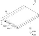
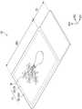
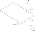
图1A是示出根据发明构思的实施例的显示装置DD的第一操作模式的透视图。图1B是示出根据发明构思的实施例的显示装置DD的第二操作模式的透视图。图1C是示出根据发明构思的实施例的显示装置DD的第三操作模式的透视图。FIG. 1A is a perspective view illustrating a first operation mode of a display device DD according to an embodiment of the inventive concept. FIG. 1B is a perspective view illustrating a second operation mode of the display device DD according to an embodiment of the inventive concept. FIG. 1C is a perspective view illustrating a third operation mode of the display device DD according to an embodiment of the inventive concept.
如图1A中所示,在第一操作模式中,其上显示图像IM的显示表面IS与由第一方向轴DR1和第二方向轴DR2限定的表面平行。显示表面IS的法线方向(即,显示装置DD的厚度方向)被指示为第三方向轴DR3。每个构件的前表面(或顶表面)和后表面(或底表面)通过第三方向轴DR3进行区分。然而,如第一方向轴DR1、第二方向轴DR2和第三方向轴DR3指示的方向可以是相对概念,因此,可以变成不同的方向。在下文中,第一方向至第三方向可以是分别由第一方向轴DR1、第二方向轴DR2和第三方向轴DR3指示的方向,并且可以分别由同样的附图标记表示。尽管在当前实施例中示出了柔性显示装置,但是发明构思的实施例不限于此。根据当前实施例的显示装置DD可以是刚性显示装置。As shown in FIG. 1A , in the first mode of operation, the display surface IS on which the image IM is displayed is parallel to the surface defined by the first direction axis DR1 and the second direction axis DR2 . The normal direction of the display surface IS (ie, the thickness direction of the display device DD) is indicated as the third direction axis DR3. The front surface (or top surface) and the rear surface (or bottom surface) of each member are distinguished by the third direction axis DR3. However, directions as indicated by the first direction axis DR1, the second direction axis DR2, and the third direction axis DR3 may be relative concepts, and thus, may become different directions. Hereinafter, the first to third directions may be directions indicated by the first direction axis DR1, the second direction axis DR2 and the third direction axis DR3, respectively, and may be denoted by the same reference numerals, respectively. Although the flexible display device is shown in the current embodiment, embodiments of the inventive concept are not limited thereto. The display device DD according to the current embodiment may be a rigid display device.
图1A至图1C示出了可折叠的显示装置作为柔性显示装置DD的示例。图2A和图2B示出了可折叠的显示装置作为柔性显示装置DD的示例。可选择地,显示装置DD可以是可卷曲的柔性显示装置,但是不具体限制。根据发明构思的实施例的柔性显示装置DD可以用于诸如电视机和监视器的大型电子装置以及诸如移动电话、台式PC、用于车辆的导航单元、游戏控制台和智能手表的中小型电子装置。1A to 1C illustrate a foldable display device as an example of the flexible display device DD. 2A and 2B illustrate a foldable display device as an example of the flexible display device DD. Alternatively, the display device DD may be a rollable flexible display device, but is not particularly limited. The flexible display device DD according to an embodiment of the inventive concept may be used for large-scale electronic devices such as televisions and monitors, as well as small and medium-sized electronic devices such as mobile phones, desktop PCs, navigation units for vehicles, game consoles, and smart watches .
如图1A中所示,柔性显示装置DD的显示表面IS可以包括多个区域。柔性显示装置DD包括其上显示有图像IM的显示区域DD-DA和与显示区域DD-DA相邻的非显示区域DD-NDA。非显示区域DD-NDA可以是其上不显示图像的区域。图1A示出花瓶作为图像IM的示例。例如,显示区域DD-DA可以具有矩形形状。非显示区域DD-NDA可以围绕显示区域DD-DA。然而,发明构思的实施例不限于此。例如,可以相对地设计显示区域DD-DA和非显示区域DD-NDA的形状。As shown in FIG. 1A , the display surface IS of the flexible display device DD may include a plurality of regions. The flexible display device DD includes a display area DD-DA on which the image IM is displayed and a non-display area DD-NDA adjacent to the display area DD-DA. The non-display area DD-NDA may be an area on which no image is displayed. FIG. 1A shows a vase as an example of an image IM. For example, the display area DD-DA may have a rectangular shape. The non-display area DD-NDA may surround the display area DD-DA. However, embodiments of the inventive concept are not limited thereto. For example, the shapes of the display area DD-DA and the non-display area DD-NDA may be relatively designed.
柔性显示装置DD可以包括壳体HS。壳体HS可以设置在柔性显示装置DD外部,以容纳内部组件。在下文中,为了便于描述,可以单独示出或不描述壳体HS。The flexible display device DD may include a housing HS. The housing HS may be disposed outside the flexible display device DD to accommodate internal components. Hereinafter, for convenience of description, the housing HS may be individually shown or not described.
如图1A至图1C中所示,显示装置DD可以包括根据操作的形式限定的多个区域。显示装置DD可以包括关于弯曲轴BX弯曲的弯曲区域BA、不弯曲的第一非弯曲区域NBA1和不弯曲的第二非弯曲区域NBA2。如图1B中所示,显示装置DD可以向内弯曲,以使第一非弯曲区域NBA1的显示表面IS和第二非弯曲区域NBA2的显示表面IS彼此面对。如图1C中所示,显示装置DD可以向外弯曲以使显示表面IS暴露于外部。As shown in FIGS. 1A to 1C , the display device DD may include a plurality of regions defined according to the form of operation. The display device DD may include a curved area BA that is curved about the curved axis BX, a first non-curved area NBA1 that is not curved, and a second non-curved area NBA2 that is not curved. As shown in FIG. 1B , the display device DD may be bent inward so that the display surface IS of the first non-curved area NBA1 and the display surface IS of the second non-curved area NBA2 face each other. As shown in FIG. 1C , the display device DD may be bent outward to expose the display surface IS to the outside.
在发明构思的实施例中,显示装置DD可以包括多个弯曲区域BA。另外,弯曲区域BA可以形成为与用于操纵显示装置DD的用户的操作对应。例如,与图1B和图1C不同,弯曲区域BA可以形成为与第一方向轴DR1平行或者形成在对角线方向上。弯曲区域BA可以具有根据其曲率半径确定的可变表面积。在发明构思的实施例中,显示装置DD可以具有仅重复图1A和图1B的操作模式的形状。In an embodiment of the inventive concept, the display device DD may include a plurality of bending areas BA. In addition, the bending area BA may be formed to correspond to the operation of the user for manipulating the display device DD. For example, unlike FIGS. 1B and 1C , the curved area BA may be formed in parallel with the first direction axis DR1 or in a diagonal direction. The curved area BA may have a variable surface area determined according to its radius of curvature. In an embodiment of the inventive concept, the display device DD may have a shape that repeats only the operation modes of FIGS. 1A and 1B .
图2A是示出根据发明构思的实施例的显示装置的第一操作模式的透视图。图2B是示出根据发明构思的实施例的显示装置的第二操作模式的透视图。图2A和图2B示出折叠非显示区域DD-NDA的显示装置作为可折叠的显示装置DD的示例。如上面所描述的,根据发明构思的实施例的显示装置DD不对弯曲区域BA和非弯曲区域NBA的数量以及弯曲区域的位置进行限制。FIG. 2A is a perspective view illustrating a first operation mode of a display device according to an embodiment of the inventive concept. FIG. 2B is a perspective view illustrating a second operation mode of the display device according to an embodiment of the inventive concept. 2A and 2B illustrate a display device in which the non-display area DD-NDA is folded as an example of the foldable display device DD. As described above, the display device DD according to an embodiment of the inventive concept does not limit the numbers of the bending areas BA and the non-bending areas NBA and the positions of the bending areas.
图3是根据发明构思的实施例的显示装置DD的剖视图。图4是根据发明构思的实施例的显示模块DM的剖视图。图3示出由第二方向轴DR2和第三方向轴DR3限定的剖视图,图4示出由第一方向轴DR1和第三方向轴DR3限定的剖视图。FIG. 3 is a cross-sectional view of a display device DD according to an embodiment of the inventive concept. FIG. 4 is a cross-sectional view of a display module DM according to an embodiment of the inventive concept. FIG. 3 shows a cross-sectional view defined by the second direction axis DR2 and the third direction axis DR3, and FIG. 4 shows a cross-sectional view defined by the first direction axis DR1 and the third direction axis DR3.
如图3中所示,显示装置DD包括保护膜PM、窗口WM、显示模块DM、第一粘合构件AM1和第二粘合构件AM2。显示模块DM设置在保护膜PM与窗口WM之间。第一粘合构件AM1结合到显示模块DM和保护膜PM,第二粘合构件AM2结合到显示模块DM和窗口WM。在发明构思的实施例中,可以省略第一粘合构件AM1和第二粘合构件AM2。可以通过涂覆工艺连续地制造保护膜PM和窗口WM。As shown in FIG. 3 , the display device DD includes a protective film PM, a window WM, a display module DM, a first adhesive member AM1 and a second adhesive member AM2. The display module DM is disposed between the protective film PM and the window WM. The first adhesive member AM1 is coupled to the display module DM and the protective film PM, and the second adhesive member AM2 is coupled to the display module DM and the window WM. In embodiments of the inventive concept, the first adhesive member AM1 and the second adhesive member AM2 may be omitted. The protective film PM and the window WM can be continuously manufactured through a coating process.
保护膜PM保护显示模块DM。保护膜PM提供了暴露于外部的第一外表面OS-L和粘合到第一粘合构件AM1的粘合表面AS1。保护膜PM防止外部湿气渗透到显示模块DM中,并吸收外部冲击。The protective film PM protects the display module DM. The protective film PM provides the first outer surface OS-L exposed to the outside and the adhesive surface AS1 to be adhered to the first adhesive member AM1. The protective film PM prevents external moisture from penetrating into the display module DM, and absorbs external shocks.
保护膜PM可以包括塑料膜。保护膜PM可以包括从由聚醚砜(PES)、聚丙烯酸酯(PAR)、聚醚酰亚胺(PEI)、聚萘二甲酸乙二醇酯(PEN)、聚对苯二甲酸乙二醇酯(PET)、聚苯硫醚(PPS)、聚烯丙基化物、聚酰亚胺(PI)、聚碳酸酯(PC)、聚(亚芳基醚砜)和它们的组合组成的组中选择的一种。The protective film PM may include a plastic film. The protective film PM can include from polyethersulfone (PES), polyacrylate (PAR), polyetherimide (PEI), polyethylene naphthalate (PEN), polyethylene terephthalate In the group consisting of ester (PET), polyphenylene sulfide (PPS), polyallyl, polyimide (PI), polycarbonate (PC), poly(arylene ether sulfone), and combinations thereof selected one.
用于形成保护膜PM的材料不限于塑料树脂。例如,保护膜PM可以包括有机/无机复合材料。保护膜PM可以包括多孔有机层和填充到多孔有机层的孔中的无机材料。保护膜PM还可以包括设置在塑料膜上的功能层。功能层可以包括树脂层。可以通过涂覆工艺来形成功能层。The material for forming the protective film PM is not limited to plastic resin. For example, the protective film PM may include an organic/inorganic composite material. The protective film PM may include a porous organic layer and an inorganic material filled into pores of the porous organic layer. The protective film PM may further include a functional layer provided on the plastic film. The functional layer may include a resin layer. The functional layer may be formed through a coating process.
窗口WM保护显示模块DM免受外部冲击,并向用户提供输入表面。窗口WM提供暴露于外部的第二外表面OS-U以及粘合到第二粘合构件AM2的粘合表面AS2。图1A至图1C的显示表面IS可以是第二外表面OS-U。The window WM protects the display module DM from external shocks and provides an input surface to the user. The window WM provides a second outer surface OS-U exposed to the outside and an adhesive surface AS2 that is adhered to the second adhesive member AM2. The display surface IS of FIGS. 1A to 1C may be the second outer surface OS-U.
在图2A和图2B的显示装置DD中,窗口WM可以不设置在弯曲区域BA上。然而,发明构思的实施例不限于此。例如,在发明构思的另一实施例中,窗口WM也可以设置在弯曲区域BA上。In the display device DD of FIGS. 2A and 2B , the window WM may not be provided on the curved area BA. However, embodiments of the inventive concept are not limited thereto. For example, in another embodiment of the inventive concept, the window WM may also be provided on the curved area BA.
显示模块DM包括通过连续的工艺一体地形成的有机发光显示面板DP和触摸感测单元TS。有机发光显示面板DP产生与输入的图像数据对应的图像(见图1A的附图标记IM)。有机发光显示面板DP提供在厚度方向DR3上彼此面对的第一显示面板表面BS1-L和第二显示面板表面BS1-U。The display module DM includes an organic light emitting display panel DP and a touch sensing unit TS integrally formed through continuous processes. The organic light emitting display panel DP generates an image corresponding to the input image data (see reference numeral IM in FIG. 1A ). The organic light emitting display panel DP provides a first display panel surface BS1-L and a second display panel surface BS1-U facing each other in the thickness direction DR3.
触摸感测单元TS获取外部输入的坐标信息。触摸感测单元TS可以直接设置在第二显示面板表面BS1-U上。在当前实施例中,触摸感测单元TS可以通过连续的工艺与有机发光显示面板DP一起制造。The touch sensing unit TS acquires externally input coordinate information. The touch sensing unit TS may be directly disposed on the second display panel surface BS1-U. In the current embodiment, the touch sensing unit TS may be manufactured together with the organic light emitting display panel DP through a continuous process.
尽管未单独示出,但是根据发明构思的实施例的显示模块DM还可以包括防反射层。防反射层可以包括滤色器、导电层/介电层/导电层的层叠结构或光学构件。防反射层可以吸收、相消干涉从外部入射的光或使从外部入射的光偏振,以减小外部光的反射率。Although not individually shown, the display module DM according to an embodiment of the inventive concept may further include an anti-reflection layer. The anti-reflection layer may include a color filter, a stacked structure of conductive layer/dielectric layer/conductive layer, or an optical member. The anti-reflection layer may absorb, destructively interfere with, or polarize light incident from the outside to reduce the reflectivity of the outside light.
第一粘合构件AM1和第二粘合构件AM2中的每个可以是光学透明粘合膜(OCA)、光学透明树脂(OCR)或压敏粘合膜(PSA)。第一粘合构件AM1和第二粘合构件AM2中的每个可以包括可光固化的粘合材料或可热固化的粘合材料。然而,发明构思的实施例不具体限制于此。Each of the first adhesive member AM1 and the second adhesive member AM2 may be an optically clear adhesive film (OCA), an optically clear resin (OCR), or a pressure-sensitive adhesive film (PSA). Each of the first adhesive member AM1 and the second adhesive member AM2 may include a photocurable adhesive material or a thermally curable adhesive material. However, embodiments of the inventive concept are not particularly limited thereto.
尽管未具体示出,但是显示装置DD还可以包括支撑功能层的框架结构,以维持图1A至图2B中示出的状态。框架结构可以包括铰接结构或铰链结构。Although not specifically shown, the display device DD may further include a frame structure supporting the functional layer to maintain the state shown in FIGS. 1A to 2B . The frame structure may include a hinged structure or a hinged structure.
如图4中所示,有机发光显示面板DP包括基体层SUB、设置在基体层SUB上的第一电路层CL1、发光器件层ELL和薄膜包封层TFE。基体层SUB可以包括至少一个塑料膜。基体层SUB可以包括塑料基底、玻璃基底、金属基底或有机/无机复合物基底作为柔性基底。As shown in FIG. 4 , the organic light emitting display panel DP includes a base layer SUB, a first circuit layer CL1 disposed on the base layer SUB, a light emitting device layer ELL, and a thin film encapsulation layer TFE. The base layer SUB may comprise at least one plastic film. The base layer SUB may include a plastic substrate, a glass substrate, a metal substrate or an organic/inorganic composite substrate as a flexible substrate.
第一电路层CL1可以包括多个绝缘层、多个导电层和半导体层。第一电路层CL1的所述多个导电层可以构成像素的信号线或电路部分。发光器件层ELL可以包括有机发光二极管OLED。薄膜包封层TFE密封发光器件层ELL。薄膜包封层TFE可以包括至少两个无机薄膜和设置在所述至少两个无机薄膜之间的有机薄膜。薄膜包封层TFE可以保护发光器件层ELL免受诸如湿气和尘土颗粒的外部物质的影响。The first circuit layer CL1 may include a plurality of insulating layers, a plurality of conductive layers, and a semiconductor layer. The plurality of conductive layers of the first circuit layer CL1 may constitute signal lines or circuit parts of the pixel. The light emitting device layer ELL may include an organic light emitting diode OLED. The thin film encapsulation layer TFE seals the light emitting device layer ELL. The thin film encapsulation layer TFE may include at least two inorganic thin films and an organic thin film disposed between the at least two inorganic thin films. The thin film encapsulation layer TFE may protect the light emitting device layer ELL from foreign substances such as moisture and dust particles.
在发明构思的当前实施例中,触摸感测单元TS可以是单层型。即,触摸感测单元TS可以包括单导电层。这里,单导电层意味着“导电层不被绝缘层划分”。第一金属层/第二金属层/金属氧化物层的层叠结构由于第一金属层和第二金属层不被金属氧化物层绝缘而可以与单导电层对应,而第一金属层/绝缘层/金属氧化物层的层叠结构可以与双导电层对应。In the current embodiment of the inventive concept, the touch sensing unit TS may be a single-layer type. That is, the touch sensing unit TS may include a single conductive layer. Here, the single conductive layer means "the conductive layer is not divided by the insulating layer". The stacked structure of the first metal layer/second metal layer/metal oxide layer may correspond to a single conductive layer since the first metal layer and the second metal layer are not insulated by the metal oxide layer, and the first metal layer/insulating layer The laminated structure of the /metal oxide layer may correspond to the double conductive layer.
可以使单导电层图案化以形成多个触摸电极和多条触摸信号线。即,触摸感测单元TS的传感器可以设置在同一层上。传感器可以直接设置在薄膜包封层TFE上。另外,触摸信号线中的每条的一部分可以与传感器设置在同一层上。触摸信号线中的每条的一部分可以设置在第一电路层CL1上。随后将详细地描述触摸感测单元TS的结构。The single conductive layer can be patterned to form multiple touch electrodes and multiple touch signal lines. That is, the sensors of the touch sensing unit TS may be disposed on the same layer. The sensor can be placed directly on the thin film encapsulation layer TFE. In addition, a portion of each of the touch signal lines may be provided on the same layer as the sensor. A portion of each of the touch signal lines may be disposed on the first circuit layer CL1. The structure of the touch sensing unit TS will be described in detail later.
触摸信号线和传感器中的每个可以包括氧化铟锡(ITO)、氧化铟锌(IZO)、氧化锌(ZnO)或氧化铟锡锌(ITZO)、PEDOT、金属纳米线和石墨烯。触摸信号线和传感器中的每个可以包括例如钼、银、钛、铜、铝和其合金的金属层。触摸信号线和传感器可以包括彼此相同的材料或彼此不同的材料。Each of the touch signal line and the sensor may include indium tin oxide (ITO), indium zinc oxide (IZO), zinc oxide (ZnO) or indium tin zinc oxide (ITZO), PEDOT, metal nanowires, and graphene. Each of the touch signal lines and sensors may include metal layers such as molybdenum, silver, titanium, copper, aluminum, and alloys thereof. The touch signal line and the sensor may include the same material as each other or different materials from each other.
当与包括多层型触摸感测构件的显示模块DM的结构相比时,根据发明构思的实施例的显示模块DM可以包括单层型触摸感测构件以简化其结构。尽管显示模块DM弯曲为图1B和图1C中所示,但是因为触摸感测单元TS细长,所以可以减小触摸感测单元TS中产生的应力。When compared with the structure of the display module DM including the multi-layer type touch sensing member, the display module DM according to the embodiment of the inventive concept may include the single-layer type touch sensing member to simplify the structure thereof. Although the display module DM is bent as shown in FIGS. 1B and 1C , since the touch sensing unit TS is elongated, stress generated in the touch sensing unit TS may be reduced.
图5是根据发明构思的实施例的有机发光显示面板DP的平面图。图6是根据发明构思的实施例的像素PX的等效电路图。图7和图8是根据发明构思的实施例的有机发光显示面板DP的局部剖视图。FIG. 5 is a plan view of an organic light emitting display panel DP according to an embodiment of the inventive concept. FIG. 6 is an equivalent circuit diagram of a pixel PX according to an embodiment of the inventive concept. 7 and 8 are partial cross-sectional views of an organic light emitting display panel DP according to an embodiment of the inventive concept.
如图5中所示,有机发光显示面板DP包括显示区域DA和非显示区域NDA。有机发光显示面板DP的显示区域DA和非显示区域NDA可以分别与显示装置DD的显示区域DD-DA和非显示区域DD-NDA对应。有机发光显示面板DP的显示区域DA和非显示区域NDA不必要分别与显示装置DD的显示区域DD-DA和非显示区域DD-NDA对应。例如,有机发光显示面板DP的显示区域DA和非显示区域NDA可以根据有机发光显示面板DP的结构/设计而变化。As shown in FIG. 5 , the organic light emitting display panel DP includes a display area DA and a non-display area NDA. The display area DA and the non-display area NDA of the organic light emitting display panel DP may correspond to the display area DD-DA and the non-display area DD-NDA of the display device DD, respectively. The display area DA and the non-display area NDA of the organic light emitting display panel DP do not necessarily correspond to the display area DD-DA and the non-display area DD-NDA of the display device DD, respectively. For example, the display area DA and the non-display area NDA of the organic light emitting display panel DP may vary according to the structure/design of the organic light emitting display panel DP.
有机发光显示面板DP可以包括多条信号线SGL和多个像素PX。其上设置有多个像素PX的区域可以被定义为显示区域DA。在当前实施例中,非显示区域NDA可以限定为沿显示区域DA的边缘并围绕显示区域DA。The organic light emitting display panel DP may include a plurality of signal lines SGL and a plurality of pixels PX. An area on which a plurality of pixels PX are disposed may be defined as a display area DA. In the current embodiment, the non-display area NDA may be defined along the edge of the display area DA and surrounding the display area DA.
多条信号线SGL包括栅极线GL、数据线DL、电源线PL和控制信号线CSL。栅极线GL连接到多个像素PX中的对应的像素,数据线DL分别连接到多个像素PX中的对应的像素PX。电源线PL连接到多个像素PX。连接有栅极线GL的栅极驱动电路DCV可以设置在非显示区域NDA的一侧上。控制信号线CSL可以向栅极驱动电路DCV提供控制信号。The plurality of signal lines SGL include gate lines GL, data lines DL, power supply lines PL, and control signal lines CSL. The gate lines GL are connected to corresponding ones of the plurality of pixels PX, and the data lines DL are respectively connected to corresponding ones of the plurality of pixels PX. The power line PL is connected to the plurality of pixels PX. The gate driving circuit DCV to which the gate line GL is connected may be disposed on one side of the non-display area NDA. The control signal line CSL may provide a control signal to the gate driving circuit DCV.
栅极线GL、数据线DL、电源线PL和控制信号线CSL的一部分可以设置在同一层上,其它部分可以设置在彼此不同的层上。当栅极线GL、数据线DL、电源线PL和控制信号线CSL中的设置在一层上的信号线被定义为第一信号线时,设置在一不同层上的信号线可以被定义为第二信号线。设置在又一层上的信号线可以被定义为第三信号线。Parts of the gate lines GL, the data lines DL, the power supply lines PL, and the control signal lines CSL may be provided on the same layer, and other parts may be provided on layers different from each other. When a signal line provided on one layer among the gate line GL, data line DL, power supply line PL and control signal line CSL is defined as the first signal line, the signal line provided on a different layer may be defined as the second signal line. A signal line disposed on a further layer may be defined as a third signal line.
栅极线GL、数据线DL、电源线PL和控制信号线CSL中的每个可以包括信号线单元和连接到信号线单元的端部的下焊盘PD-D。信号线单元可以被定义为除了栅极线GL、数据线DL、电源线PL和控制信号线CSL中的每个的下焊盘PD-D之外的部分。Each of the gate line GL, the data line DL, the power supply line PL, and the control signal line CSL may include a signal line unit and a lower pad PD-D connected to an end of the signal line unit. The signal line unit may be defined as a portion other than the lower pad PD-D of each of the gate line GL, the data line DL, the power supply line PL, and the control signal line CSL.
在发明构思的实施例中,下焊盘PD-D可以包括下显示面板焊盘PD-DPD和下触摸感测构件焊盘PD-TSD。可以通过与用于驱动像素PX的晶体管的工艺相同的工艺来形成下焊盘PD-D。例如,可以通过相同的低温多晶硅(LTPS)工艺或低温多晶氧化物(LTPO)工艺来形成用于驱动像素PX的晶体管和下焊盘PD-D。In an embodiment of the inventive concept, the lower pad PD-D may include a lower display panel pad PD-DPD and a lower touch sensing member pad PD-TSD. The lower pad PD-D may be formed through the same process as that used to drive the transistor of the pixel PX. For example, the transistor for driving the pixel PX and the lower pad PD-D may be formed through the same low temperature polysilicon (LTPS) process or low temperature polycrystalline oxide (LTPO) process.
在发明构思的实施例中,下显示面板焊盘PD-DPD可以包括控制焊盘CSL-P、数据焊盘DL-P和电源焊盘PL-P。尽管未示出栅极焊盘单元,但是栅极焊盘单元可以与栅极驱动电路DCV叠置,并连接到栅极驱动电路DCV。尽管未具体示出,但是非显示区域NDA的其上使控制焊盘CSL-P、数据焊盘DL-P和电源焊盘PL-P对齐的部分被定义为焊盘区域。如下面所描述的,触摸感测单元TS的焊盘可以设置为与上面描述的有机发光显示面板DP的焊盘相邻。In embodiments of the inventive concept, the lower display panel pads PD-DPD may include control pads CSL-P, data pads DL-P, and power pads PL-P. Although the gate pad unit is not shown, the gate pad unit may overlap with the gate driving circuit DCV and be connected to the gate driving circuit DCV. Although not specifically shown, a portion of the non-display area NDA on which the control pad CSL-P, the data pad DL-P, and the power pad PL-P are aligned is defined as a pad area. As described below, the pads of the touch sensing unit TS may be disposed adjacent to the pads of the organic light emitting display panel DP described above.
图6示出连接到一条栅极线GL、一条数据线DL和电源线PL的像素PX的示例。然而,发明构思的实施例不限于像素PX的构造。例如,像素PX可以具有各种构造。FIG. 6 shows an example of a pixel PX connected to one gate line GL, one data line DL, and a power supply line PL. However, embodiments of the inventive concept are not limited to the configuration of the pixels PX. For example, the pixels PX may have various configurations.
像素PX包括有机发光二极管OLED作为显示器件。有机发光二极管OLED可以是顶发射型二极管或底发射型二极管。像素PX包括第一晶体管TFT1(或开关晶体管)、第二晶体管TFT2(或驱动晶体管)和电容器CP作为用于驱动有机发光二极管OLED的电路单元。有机发光二极管OLED响应于从晶体管TFT1和TFT2提供的电信号而产生光。有机发光二极管OLED的阴极连接到第二电源电压(ELVSS)。The pixel PX includes an organic light emitting diode OLED as a display device. The organic light emitting diode OLED may be a top-emitting diode or a bottom-emitting diode. The pixel PX includes a first transistor TFT1 (or a switching transistor), a second transistor TFT2 (or a driving transistor) and a capacitor CP as circuit units for driving the organic light emitting diode OLED. The organic light emitting diode OLED generates light in response to electrical signals supplied from the transistors TFT1 and TFT2. The cathode of the organic light emitting diode OLED is connected to the second power supply voltage (ELVSS).
栅极线GL可以用来接收第一电源电压(ELVDD)。第一晶体管TFT1响应于施加到栅极线GL的扫描信号而输出施加到数据线DL的数据信号。电容器CP充入与从第一晶体管TFT1接收的数据信号对应的电压。The gate line GL may be used to receive the first power supply voltage (ELVDD). The first transistor TFT1 outputs a data signal applied to the data line DL in response to the scan signal applied to the gate line GL. The capacitor CP is charged with a voltage corresponding to the data signal received from the first transistor TFT1.
第二晶体管TFT2连接到有机发光二极管OLED。第二晶体管TFT2控制流经有机发光二极管OLED的驱动电流,以与电容器CP中存储的电荷量对应。有机发光二极管OLED在第二晶体管TFT2的导通期间发射光。The second transistor TFT2 is connected to the organic light emitting diode OLED. The second transistor TFT2 controls the driving current flowing through the organic light emitting diode OLED to correspond to the amount of charge stored in the capacitor CP. The organic light emitting diode OLED emits light during the turn-on period of the second transistor TFT2.
图7是与图6的等效电路的第一晶体管TFT1和电容器CP对应的部分的剖视图。图8是与图6的等效电路的第二晶体管TFT2和有机发光二极管OLED对应的部分的剖视图。FIG. 7 is a cross-sectional view of a portion corresponding to the first transistor TFT1 and the capacitor CP of the equivalent circuit of FIG. 6 . FIG. 8 is a cross-sectional view of a portion corresponding to the second transistor TFT2 and the organic light emitting diode OLED of the equivalent circuit of FIG. 6 .
如图7和图8中所示,第一电路层CL1设置在基体层SUB上。第一晶体管TFT1的半导体图案AL1(在下文中,被称作第一半导体图案)和第二晶体管TFT2的半导体图案AL2(在下文中,被称作第二半导体图案)设置在基体层SUB上。第一半导体图案AL1和第二半导体图案AL2可以选自于非晶硅、多晶硅和金属氧化物半导体。第一半导体图案AL1和第二半导体图案AL2可以由相同的材料形成。第一半导体图案AL1和第二半导体图案AL2可以由不同的材料形成。As shown in FIGS. 7 and 8 , the first circuit layer CL1 is provided on the base layer SUB. A semiconductor pattern AL1 (hereinafter, referred to as a first semiconductor pattern) of the first transistor TFT1 and a semiconductor pattern AL2 (hereinafter, referred to as a second semiconductor pattern) of the second transistor TFT2 are disposed on the base layer SUB. The first semiconductor pattern AL1 and the second semiconductor pattern AL2 may be selected from amorphous silicon, polysilicon, and metal oxide semiconductors. The first semiconductor pattern AL1 and the second semiconductor pattern AL2 may be formed of the same material. The first semiconductor pattern AL1 and the second semiconductor pattern AL2 may be formed of different materials.
第一电路层CL1包括第一导电图案(见图12的附图标记CDP1)以及有机/无机层BR、BF、12、14和16。第一导电图案(见图12的附图标记CDP1)可以包括第一晶体管TFT1、第二晶体管TFT2以及电极E1和E2。有机/无机层BR、BF、12、14和16可以包括第一功能层BR和BF、第一绝缘层12、第二绝缘层14以及第三绝缘层16。The first circuit layer CL1 includes a first conductive pattern (see reference numeral CDP1 in FIG. 12 ) and organic/inorganic layers BR, BF, 12 , 14 and 16 . The first conductive pattern (see reference numeral CDP1 in FIG. 12 ) may include a first transistor TFT1 , a second transistor TFT2 , and electrodes E1 and E2 . The organic/inorganic layers BR, BF, 12 , 14 and 16 may include first functional layers BR and BF, a first insulating
第一功能层BR和BF可以设置在基体层SUB的一个表面上。第一功能层BR和BF可以包括阻挡层BR和缓冲层BF中的至少一个。第一半导体图案AL1和第二半导体图案AL2可以设置在阻挡层BR或缓冲层BF上。The first functional layers BR and BF may be provided on one surface of the base layer SUB. The first functional layers BR and BF may include at least one of a barrier layer BR and a buffer layer BF. The first semiconductor pattern AL1 and the second semiconductor pattern AL2 may be disposed on the barrier layer BR or the buffer layer BF.
覆盖第一半导体图案AL1和第二半导体图案AL2的第一绝缘层12设置在基体层SUB上。第一绝缘层12包括有机层和/或无机层。具体地,第一绝缘层12可以包括多个无机薄膜。所述多个无机薄膜可以包括氮化硅层和氧化硅层。The first insulating
第一晶体管TFT1的控制电极GE1(在下文中,被称作第一控制电极)和第二晶体管TFT2的控制电极GE2(在下文中,被称作第二控制电极)设置在第一绝缘层12上。电容器CP的第一电极E1设置在第一绝缘层12上。可以通过与栅极线GL(见图5)的光刻工艺相同的光刻工艺来制造第一控制电极GE1、第二控制电极GE2和第一电极E1。即,第一控制电极GE1、第二控制电极GE2和第一电极E1可以由与栅极线GL的材料相同的材料来形成,具有与栅极线GL的层叠结构相同的层叠结构,并与栅极线GL设置在同一层上。A control electrode GE1 (hereinafter, referred to as a first control electrode) of the first transistor TFT1 and a control electrode GE2 (hereinafter, referred to as a second control electrode) of the second transistor TFT2 are provided on the first insulating
覆盖第一控制电极GE1和第二控制电极GE2以及第一电极E1的第二绝缘层14设置在第一绝缘层12上。第二绝缘层14包括有机层和/或无机层。具体地,第二绝缘层14可以包括多个无机薄膜。所述多个无机薄膜可以包括氮化硅层和氧化硅层。The second insulating
数据线DL(见图5)可以设置在第二绝缘层14上。第一晶体管TFT1的输入电极SE1(在下文中,被称作第一输入电极)和输出电极DE1(在下文中,被称作第一输出电极)设置在第二绝缘层14上。第二晶体管TFT2的输入电极SE2(在下文中,被称作第二输入电极)和输出电极DE2(在下文中,被称作第二输出电极)设置在第二绝缘层14上。第一输入电极SE1从数据线DL的对应数据线分支。电源线PL(见图5)可以与数据线DL设置在同一层上。第二输入电极SE2可以从电源线PL分支。The data line DL (see FIG. 5 ) may be disposed on the second insulating
电容器CP的第二电极E2设置在第二绝缘层14上。可以通过与数据线DL和电源线PL中的每个的光刻工艺相同的光刻工艺来制造第二电极E2。另外,第二电极E2可以由与数据线DL和电源线PL中的每个的材料相同的材料形成,具有与数据线DL和电源线PL中的每个的结构相同的结构,并与数据线DL和电源线PL中的每个设置在同一层上。The second electrode E2 of the capacitor CP is provided on the second insulating
第一输入电极SE1和第一输出电极DE1分别通过穿过第一绝缘层12和第二绝缘层14的第一通孔CH1和第二通孔CH2连接到第一半导体图案AL1。第一输出电极DE1可以电连接到第一电极E1。例如,第一输出电极DE1可以通过穿过第二绝缘层14的通孔(未示出)连接到第一电极E1。第二输入电极SE2和第二输出电极DE2分别通过穿过第一绝缘层12和第二绝缘层14的第三通孔CH3和第四通孔CH4连接到第二半导体图案AL2。根据发明构思的另一实施例,第一晶体管TFT1和第二晶体管TFT2中的每个可以具有底栅结构。The first input electrode SE1 and the first output electrode DE1 are connected to the first semiconductor pattern AL1 through first and second through holes CH1 and CH2 passing through the first insulating
覆盖第一输入电极SE1、第一输出电极DE1、第二输入电极SE2和第二输出电极DE2的第三绝缘层16设置在第二绝缘层14上。第三绝缘层16包括有机层和/或无机层。具体地,第三绝缘层16可以包括有机材料以提供平坦表面。A third insulating
可以根据像素的电路结构省略第一绝缘层12、第二绝缘层14和第三绝缘层16中的一个。第二绝缘层14和第三绝缘层16中的每个可以被定义为层间介电层。层间介电层可以设置在下导电图案与上导电图案之间,以使导电图案彼此绝缘,下导电图案设置在层间介电层下方,上导电图案设置在层间介电层上方。One of the first insulating
第一电路层CL1包括虚设导电图案。虚设导电图案与半导体图案AL1和AL2、控制电极GE1和GE2或者输出电极DE1和DE2设置在同一层上。虚设导电图案可以设置在非显示区域NDA(见图5)上。随后将详细地描述虚设导电图案。The first circuit layer CL1 includes dummy conductive patterns. The dummy conductive patterns are disposed on the same layer as the semiconductor patterns AL1 and AL2, the control electrodes GE1 and GE2, or the output electrodes DE1 and DE2. Dummy conductive patterns may be disposed on the non-display area NDA (see FIG. 5). The dummy conductive pattern will be described in detail later.
发光器件层ELL设置在第三绝缘层16上。像素限定层PXL和有机发光二极管OLED设置在第三绝缘层16上。阳极AE设置在第三绝缘层16上。阳极AE通过穿过第三绝缘层16的第五通孔CH5连接到第二输出电极DE2。开口OP限定在像素限定层PXL中。像素限定层PXL的开口OP暴露阳极AE的至少一部分。The light emitting device layer ELL is disposed on the third insulating
发光器件层ELL可以包括发射区域PXA和与发射区域PXA相邻的非发射区域NPXA。非发射区域NPXA可以围绕发射区域PXA。在当前实施例中,发射区域PXA被限定为与阳极AE对应。然而,发明构思的实施例不限于上面描述的发射区域PXA。即,如果从区域发射光,则该区域可以被定义为发射区域PXA。发射区域PXA可以被限定为与阳极AE的通过开口OP暴露的一部分对应。The light emitting device layer ELL may include an emission area PXA and a non-emission area NPXA adjacent to the emission area PXA. The non-emission area NPXA may surround the emission area PXA. In the current embodiment, the emission area PXA is defined to correspond to the anode AE. However, embodiments of the inventive concept are not limited to the above-described emission area PXA. That is, if light is emitted from an area, the area may be defined as an emission area PXA. The emission area PXA may be defined to correspond to a portion of the anode AE exposed through the opening OP.
空穴控制层HCL可以公共地设置在发射区域PXA和非发射区域NPXA上。尽管未具体示出,但是诸如空穴控制层HCL的公共层可以公共地设置在多个像素PX(见图5)上。The hole control layer HCL may be disposed on the emission region PXA and the non-emission region NPXA in common. Although not specifically shown, a common layer such as a hole control layer HCL may be commonly provided on a plurality of pixels PX (see FIG. 5 ).
有机发光层EML设置在空穴控制层HCL上。有机发光层EML可以被设置为覆盖开口OP。彼此相邻的有机发光层EML彼此电分离。The organic light emitting layer EML is disposed on the hole control layer HCL. The organic light emitting layer EML may be disposed to cover the opening OP. The organic light-emitting layers EML adjacent to each other are electrically separated from each other.
电子控制层ECL设置在有机发光层EML上。阴极CE设置在电子控制层ECL上。阴极CE公共地设置在多个像素PX上。The electron control layer ECL is disposed on the organic light emitting layer EML. The cathode CE is disposed on the electron control layer ECL. The cathodes CE are commonly provided on the plurality of pixels PX.
尽管将图案化的有机发光层EML示出为当前实施例中的示例,但是有机发光层EML可以公共地设置在多个像素PX上。这里,有机发光层EML可以发射白光。另外,有机发光层EML可以具有多层结构。Although the patterned organic light emitting layer EML is shown as an example in the current embodiment, the organic light emitting layer EML may be provided on a plurality of pixels PX in common. Here, the organic light emitting layer EML may emit white light. In addition, the organic light emitting layer EML may have a multilayer structure.
在当前实施例中,薄膜包封层TFE直接覆盖阴极CE。在当前实施例中,还可以设置覆盖阴极CE的覆层。这里,薄膜包封层TFE直接覆盖覆层。薄膜包封层TFE可以包括包含有机材料的有机层和包含无机材料的无机层。In the current embodiment, the thin film encapsulation layer TFE directly covers the cathode CE. In the current embodiment, a cladding layer covering the cathode CE may also be provided. Here, the thin-film encapsulation layer TFE directly covers the cladding layer. The thin film encapsulation layer TFE may include an organic layer including an organic material and an inorganic layer including an inorganic material.
图9是根据发明构思的实施例的触摸感测单元TS的平面图。FIG. 9 is a plan view of a touch sensing unit TS according to an embodiment of the inventive concept.
在当前实施例中,将1层电容式触摸感测构件TS示出为示例。1层电容式触摸感测构件TS可以以自电容方式或互电容方式来驱动。然而,发明构思的实施例不限于用于获取坐标信息的驱动方式。另外,触摸感测构件TS可以不限于1层结构。例如,触摸感测构件TS可以具有2层结构。In the current embodiment, a 1-layer capacitive touch sensing member TS is shown as an example. The 1-layer capacitive touch sensing member TS may be driven in a self-capacitance manner or a mutual capacitance manner. However, the embodiments of the inventive concept are not limited to the driving manner for acquiring the coordinate information. In addition, the touch sensing member TS may not be limited to a 1-layer structure. For example, the touch sensing member TS may have a 2-layer structure.
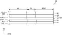
触摸感测构件TS可以包括第一触摸图案TE1-1至TE-3、第一触摸信号线SL1、第二触摸图案TE2-1至TE2-3、第二触摸信号线SL2和触摸感测构件焊盘上焊盘PD-U。The touch sensing member TS may include first touch patterns TE1-1 to TE-3, first touch signal lines SL1, second touch patterns TE2-1 to TE2-3, second touch signal lines SL2 and touch sensing member pads On-disk pad PD-U.
第一触摸图案TE1-1至TE1-3在第一方向DR1上延伸,并布置在第二方向DR2上。第一触摸图案TE1-1至TE1-3中的每个可以具有限定多个触摸开口OP-TC的网格形状。The first touch patterns TE1-1 to TE1-3 extend in the first direction DR1 and are arranged in the second direction DR2. Each of the first touch patterns TE1-1 to TE1-3 may have a mesh shape defining a plurality of touch openings OP-TC.
第一触摸图案TE1-1至TE1-3中的每个包括多个第一感测图案SP1和多个第一连接图案CP1。第一感测图案SP1布置在第一方向DR1上。第一连接图案CP1中的每个将沿第一方向DR1布置的两个相邻的第一感测图案SP1连接。Each of the first touch patterns TE1-1 to TE1-3 includes a plurality of first sensing patterns SP1 and a plurality of first connection patterns CP1. The first sensing patterns SP1 are arranged in the first direction DR1. Each of the first connection patterns CP1 connects two adjacent first sensing patterns SP1 arranged in the first direction DR1.
第一触摸信号线SL1中的每条可以连接到第一触摸图案TE1-1至TE1-3的一端,并连接到焊盘区域中的焊盘。第一触摸信号线SL1可以具有与第一触摸图案TE1-1至TE1-3的层结构相同的层结构。Each of the first touch signal lines SL1 may be connected to one end of the first touch patterns TE1-1 to TE1-3 and connected to pads in the pad area. The first touch signal line SL1 may have the same layer structure as that of the first touch patterns TE1-1 to TE1-3.
第二触摸图案TE2-1至TE2-3与第一触摸图案TE1-1至TE1-3绝缘,并与第一触摸图案TE1-1至TE1-3交叉。第二触摸图案TE2-1至TE2-3通过绝缘图案IL-P与第一触摸图案TE1-1至TE1-3绝缘。绝缘图案IL-P可以包括无机材料或有机材料。无机材料可以包括氧化硅或氮化硅。有机材料可以包括丙烯酸类树脂、甲基丙烯酸类树脂、聚异戊二烯类树脂、乙烯基类树脂、环氧类树脂、聚氨酯类树脂、纤维素类树脂和苝类树脂中的至少一种。The second touch patterns TE2-1 to TE2-3 are insulated from the first touch patterns TE1-1 to TE1-3 and intersect with the first touch patterns TE1-1 to TE1-3. The second touch patterns TE2-1 to TE2-3 are insulated from the first touch patterns TE1-1 to TE1-3 by the insulating pattern IL-P. The insulating pattern IL-P may include an inorganic material or an organic material. The inorganic material may include silicon oxide or silicon nitride. The organic material may include at least one of acrylic resin, methacrylic resin, polyisoprene-based resin, vinyl-based resin, epoxy-based resin, urethane-based resin, cellulose-based resin, and perylene-based resin.
第二触摸图案TE2-1至TE2-3中的每个可以具有限定多个触摸开口OP-TC的网格形状。Each of the second touch patterns TE2-1 to TE2-3 may have a mesh shape defining a plurality of touch openings OP-TC.
第二触摸图案TE2-1至TE2-3中的每个包括多个第二感测图案SP2和多个第二连接图案CP2。第二感测图案SP2布置在第二方向DR2上。第二连接图案CP2中的每个将沿第二方向DR2布置的两个相邻的第二感测图案SP2连接。Each of the second touch patterns TE2-1 to TE2-3 includes a plurality of second sensing patterns SP2 and a plurality of second connection patterns CP2. The second sensing patterns SP2 are arranged in the second direction DR2. Each of the second connection patterns CP2 connects two adjacent second sensing patterns SP2 arranged in the second direction DR2.
第二连接图案CP2中的每个可以具有桥接功能。绝缘图案IL-P设置在第一连接图案CP1上,第二连接图案CP2设置在绝缘图案IL-P上。Each of the second connection patterns CP2 may have a bridge function. The insulating pattern IL-P is disposed on the first connection pattern CP1, and the second connection pattern CP2 is disposed on the insulating pattern IL-P.
第二触摸信号线SL2中的每条也可以连接到第二触摸图案TE2-1至TE2-3的一端,并连接到焊盘区域中的焊盘。第二触摸信号线SL2可以具有与第二触摸图案TE2-1至TE2-3层结构相同的层结构。Each of the second touch signal lines SL2 may also be connected to one end of the second touch patterns TE2-1 to TE2-3 and connected to pads in the pad area. The second touch signal line SL2 may have the same layer structure as that of the second touch patterns TE2-1 to TE2-3.
第一触摸图案TE1-1至TE1-3以及第二触摸图案TE2-1至TE2-3彼此电容耦合。由于触摸感测信号被施加到第一触摸图案TE1-1至TE1-3,因此电容器设置在第一感测图案SP1与第二感测图案SP2之间。The first touch patterns TE1-1 to TE1-3 and the second touch patterns TE2-1 to TE2-3 are capacitively coupled to each other. Since the touch sensing signals are applied to the first touch patterns TE1-1 to TE1-3, capacitors are disposed between the first and second sensing patterns SP1 and SP2.
第一触摸图案TE1-1至TE1-3和第二触摸图案TE2-1至TE2-3的形状可以仅是示例,因此,发明构思的实施例不限于此。例如,连接图案CP1和CP2可以限定为第一触摸图案TE1-1至TE1-3与第二触摸图案TE2-1至TE2-3彼此交叉的部分,感测图案SP1和SP2可以限定为第一触摸图案TE1-1至TE1-3和第二触摸图案TE2-1至TE2-3彼此不叠置的部分。例如,第一触摸图案TE1-1至TE1-3和第二触摸图案TE2-1至TE2-3中的每个可以具有条形状,所述条形状具有预定宽度。The shapes of the first touch patterns TE1-1 to TE1-3 and the second touch patterns TE2-1 to TE2-3 may be only examples, and thus, embodiments of the inventive concept are not limited thereto. For example, the connection patterns CP1 and CP2 may be defined as portions where the first touch patterns TE1-1 to TE1-3 and the second touch patterns TE2-1 to TE2-3 cross each other, and the sensing patterns SP1 and SP2 may be defined as the first touch patterns Parts where the patterns TE1-1 to TE1-3 and the second touch patterns TE2-1 to TE2-3 do not overlap each other. For example, each of the first touch patterns TE1-1 to TE1-3 and the second touch patterns TE2-1 to TE2-3 may have a bar shape having a predetermined width.
触摸感测构件焊盘上焊盘PD-U可以设置在第一触摸信号线SL1和第二触摸信号线SL2的末端上。触摸感测构件焊盘上焊盘PD-U可以包括上显示面板焊盘PD-PDU和上触摸感测构件焊盘PD-TSU。可以通过与第一触摸图案TE1-1至TE-3、第一触摸信号线SL1、第二触摸图案TE2-1至TE2-3和第二触摸信号线SL2的工艺相同的工艺来形成触摸感测构件焊盘上焊盘PD-U。The touch-sensing member-on-pad pad PD-U may be disposed on ends of the first touch signal line SL1 and the second touch signal line SL2. The upper touch sensing member pads PD-U may include an upper display panel pad PD-PDU and an upper touch sensing member pad PD-TSU. The touch sensing may be formed through the same process as that of the first touch patterns TE1-1 to TE-3, the first touch signal lines SL1, the second touch patterns TE2-1 to TE2-3, and the second touch signal lines SL2 Pad PD-U on component pad.
图10是图9的部分AA的放大视图。图11是沿图10的线I-I'截取的剖视图。FIG. 10 is an enlarged view of part AA of FIG. 9 . FIG. 11 is a cross-sectional view taken along line II′ of FIG. 10 .
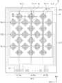
显示区域DA包括多个发射区域PXA和围绕多个发射区域PXA的非发射区域NPXA。第一感测图案SP1可以具有与非发射区域NPXA叠置的网格形状。尽管未具体示出,但是第二感测图案SP2以及触摸信号线SL1和SL2也可以具有与非发射区域NPXA叠置的网格形状。The display area DA includes a plurality of emission areas PXA and a non-emission area NPXA surrounding the plurality of emission areas PXA. The first sensing pattern SP1 may have a mesh shape overlapping with the non-emission area NPXA. Although not specifically shown, the second sensing pattern SP2 and the touch signal lines SL1 and SL2 may also have a mesh shape overlapping the non-emission area NPXA.
第一感测图案SP1包括在第一方向DR1上延伸的多个竖直部分SP1-C和在第二方向DR2上延伸的多个水平部分SP1-L。多个竖直部分SP1-C和多个水平部分SP1-L可以被限定为网格线。所述网格线可以具有几微米的线宽。The first sensing pattern SP1 includes a plurality of vertical portions SP1-C extending in the first direction DR1 and a plurality of horizontal portions SP1-L extending in the second direction DR2. The plurality of vertical parts SP1-C and the plurality of horizontal parts SP1-L may be defined as grid lines. The grid lines may have line widths of several micrometers.
多个竖直部分SP1-C和多个水平部分SP1-L可以彼此连接以限定多个触摸开口TS-OP。尽管示出了触摸开口TS-OP与发射区域PXA一一对应的结构,但是发明构思的实施例不限于此。一个触摸开口TS-OP可以与两个或更多个发射区域PXA对应。尽管图10和图11中示出了暴露于外部的网格线,但是显示模块DM(见图4)还可以包括设置在薄膜包封层TFE上的绝缘层以覆盖网格线。A plurality of vertical parts SP1-C and a plurality of horizontal parts SP1-L may be connected to each other to define a plurality of touch openings TS-OP. Although the structure in which the touch openings TS-OP and the emission areas PXA correspond one-to-one is shown, embodiments of the inventive concept are not limited thereto. One touch opening TS-OP may correspond to two or more emission areas PXA. Although the grid lines exposed to the outside are shown in FIGS. 10 and 11 , the display module DM (see FIG. 4 ) may further include an insulating layer disposed on the thin film encapsulation layer TFE to cover the grid lines.
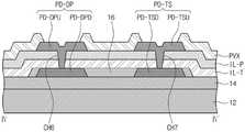
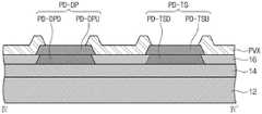
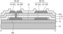
图12是图5和图9的显示面板焊盘PD-DP和触摸感测构件焊盘PD-TS的视图。显示模块DM可以包括有源区域AR-ACV、焊盘区域AR-PD和设置在有源区域AR-ACV与焊盘区域AR-PD之间的边界区域AR-BD。FIG. 12 is a view of the display panel pad PD-DP and the touch sensing member pad PD-TS of FIGS. 5 and 9 . The display module DM may include an active area AR-ACV, a pad area AR-PD, and a border area AR-BD disposed between the active area AR-ACV and the pad area AR-PD.
在有源区域AR-ACV中,显示模块DM包括第一导电图案CDP1。在焊盘区域AR-PD中,显示模块DM包括第二导电图案CDP2。在边界区域AR-BD中,显示模块DM包括第三导电图案CDP3。第一导电图案CDP1至第三导电图案CDP3中的每个可以包括金属作为用于传导电信号的图案,所述电信号用于驱动显示面板DP或触摸感测构件TS。In the active area AR-ACV, the display module DM includes a first conductive pattern CDP1. In the pad area AR-PD, the display module DM includes the second conductive pattern CDP2. In the border area AR-BD, the display module DM includes the third conductive pattern CDP3. Each of the first to third conductive patterns CDP1 to CDP3 may include metal as a pattern for conducting electrical signals for driving the display panel DP or the touch sensing member TS.
显示面板焊盘PD-DP和触摸感测构件焊盘PD-TS可以设置为彼此相邻。另外,显示面板焊盘PD-DP和触摸感测构件焊盘PD-TS可以设置为彼此平行。然而,发明构思的实施例不限于此。例如,如有必要,显示面板焊盘PD-DP和触摸感测构件焊盘PD-TS可以彼此分隔开,但不设置为彼此平行。The display panel pads PD-DP and the touch sensing member pads PD-TS may be disposed adjacent to each other. In addition, the display panel pads PD-DP and the touch sensing member pads PD-TS may be disposed parallel to each other. However, embodiments of the inventive concept are not limited thereto. For example, if necessary, the display panel pads PD-DP and the touch sensing member pads PD-TS may be spaced apart from each other, but not arranged to be parallel to each other.
图13A是沿图12的线II-II'截取的剖视图。图13B是沿图12的线III-III'截取的剖视图。图13C是沿图12的线IV-IV'截取的剖视图。图13A至图13C示出了发明构思的实施例。FIG. 13A is a cross-sectional view taken along line II-II′ of FIG. 12 . FIG. 13B is a cross-sectional view taken along line III-III′ of FIG. 12 . FIG. 13C is a cross-sectional view taken along line IV-IV' of FIG. 12 . 13A to 13C illustrate embodiments of the inventive concept.
参照示出了触摸感测构件焊盘的图13A,基体层SUB包括有源区域AR-ACV、焊盘区域AR-PD和设置在有源区域AR-ACV与焊盘区域AR-PD之间的边界区域AR-BD。Referring to FIG. 13A showing the touch sensing member pad, the base layer SUB includes an active area AR-ACV, a pad area AR-PD, and a pad area AR-PD disposed between the active area AR-ACV and the pad area AR-PD Border area AR-BD.
在根据发明构思的实施例的有源区域AR-ACV、焊盘区域AR-PD和边界区域AR-BD中,有源区域AR-ACV可以是包括发光器件层ELL的区域,焊盘区域AR-PD可以是包括从印刷电路板向其施加信号的显示面板焊盘PD-DP和触摸感测构件焊盘PD-TS的区域,边界区域AR-BD可以是有源区域AR-ACV与焊盘区域AR-PD之间的区域。In the active area AR-ACV, the pad area AR-PD, and the border area AR-BD according to embodiments of the inventive concept, the active area AR-ACV may be an area including the light emitting device layer ELL, the pad area AR- The PD may be an area including the display panel pad PD-DP and the touch sensing member pad PD-TS to which signals are applied from the printed circuit board, and the border area AR-BD may be the active area AR-ACV and the pad area The area between AR-PD.
电路层CL1和CL2设置在基体层SUB上。电路层CL1和CL2包括第一电路层CL1和第二电路层CL2。第一电路层CL1设置在基体层SUB的有源区域AR-ACV上。第二电路层CL2设置在基体层SUB的焊盘区域AR-PD上。The circuit layers CL1 and CL2 are provided on the base layer SUB. The circuit layers CL1 and CL2 include a first circuit layer CL1 and a second circuit layer CL2. The first circuit layer CL1 is disposed on the active area AR-ACV of the base layer SUB. The second circuit layer CL2 is disposed on the pad region AR-PD of the base layer SUB.
发光器件层ELL和薄膜包封层TFE设置在第一电路层CL1上。第一电路层CL1和第二电路层CL2可以分别包括功能层BR和BF。为了方便,在功能层BR和BF中,第一电路层CL1的功能层可以被称作第一功能层,第二电路层CL2的功能层可以被称作第二功能层。The light emitting device layer ELL and the thin film encapsulation layer TFE are disposed on the first circuit layer CL1. The first circuit layer CL1 and the second circuit layer CL2 may include functional layers BR and BF, respectively. For convenience, in the functional layers BR and BF, the functional layer of the first circuit layer CL1 may be referred to as the first functional layer, and the functional layer of the second circuit layer CL2 may be referred to as the second functional layer.
因为图7和图8中示出了第一电路层CL1、发光器件层ELL和薄膜包封层TFE,所以将省略其详细的描述。Since the first circuit layer CL1 , the light emitting device layer ELL, and the thin film encapsulation layer TFE are shown in FIGS. 7 and 8 , detailed descriptions thereof will be omitted.
触摸感测构件TS可以设置在薄膜包封层TFE上。触摸感测构件TS在剖面上包括触摸无机层IL-T、绝缘图案IL-P、多个触摸电极和触摸保护层PVX。触摸无机层IL-T和绝缘图案IL-P中的每个可以包括无机材料。触摸保护层PVX可以包括有机材料。The touch sensing member TS may be disposed on the thin film encapsulation layer TFE. The touch sensing member TS includes, in cross section, a touch inorganic layer IL-T, an insulating pattern IL-P, a plurality of touch electrodes, and a touch protection layer PVX. Each of the touch inorganic layer IL-T and the insulating pattern IL-P may include an inorganic material. The touch protection layer PVX may include organic materials.
参照图9,多个触摸电极可以形成第一触摸图案TE1-1至TE1-3、第一触摸信号线SL1、第二触摸图案TE2-1至TE2-3和第二触摸信号线SL2。9, a plurality of touch electrodes may form first touch patterns TE1-1 to TE1-3, first touch signal lines SL1, second touch patterns TE2-1 to TE2-3, and second touch signal lines SL2.
第二电路层CL2可以包括第二导电图案CDP2(见图12)以及有机/无机层BR、BF、12、14和16。第二导电图案CDP2可以包括显示面板焊盘PD-DP和触摸感测构件焊盘PD-TS。有机/无机层BR、BF、12、14和16可以包括第二功能层BR和BF、第一绝缘层12、第二绝缘层14和第三绝缘层16。The second circuit layer CL2 may include a second conductive pattern CDP2 (see FIG. 12 ) and organic/inorganic layers BR, BF, 12 , 14 and 16 . The second conductive pattern CDP2 may include display panel pads PD-DP and touch sensing member pads PD-TS. The organic/inorganic layers BR, BF, 12 , 14 and 16 may include second functional layers BR and BF, a first insulating
显示面板焊盘PD-DP可以设置在第二功能层上,并电连接到第一电路层CL1。第一绝缘层12和第二绝缘层14中的至少一个可以设置在显示面板焊盘PD-DP与第二功能层之间。The display panel pad PD-DP may be disposed on the second functional layer and electrically connected to the first circuit layer CL1. At least one of the first insulating
显示面板焊盘PD-DP可以包括下显示面板焊盘PD-DPD和上显示面板焊盘PD-DPU。下显示面板焊盘PD-DPD通过第三导电图案CDP3电连接到第一导电图案CDP1。上显示面板焊盘PD-DPU设置在下显示面板焊盘PD-DPD上,并电连接到下显示面板焊盘PD-DPD。因此,施加到上显示面板焊盘PD-DPU的电信号经由下显示面板焊盘PD-DPD被施加到第一电路层CL1的第一导电图案CDP1。The display panel pads PD-DP may include a lower display panel pad PD-DPD and an upper display panel pad PD-DPU. The lower display panel pad PD-DPD is electrically connected to the first conductive pattern CDP1 through the third conductive pattern CDP3. The upper display panel pad PD-DPU is disposed on the lower display panel pad PD-DPD, and is electrically connected to the lower display panel pad PD-DPD. Accordingly, the electrical signal applied to the upper display panel pad PD-DPU is applied to the first conductive pattern CDP1 of the first circuit layer CL1 via the lower display panel pad PD-DPD.
边界层BDL设置在基体层SUB的边界区域AR-BD上。边界层BDL可以包括有机层OG和第三导电图案CDP3。有机层OG可以接触基体层SUB的顶表面,并设置在第一电路层CL1与第二电路层CL2之间。更具体地,有机层OG可以设置在第一功能层与第二功能层之间。The boundary layer BDL is provided on the boundary region AR-BD of the base layer SUB. The boundary layer BDL may include the organic layer OG and the third conductive pattern CDP3. The organic layer OG may contact the top surface of the base layer SUB and be disposed between the first circuit layer CL1 and the second circuit layer CL2. More specifically, the organic layer OG may be disposed between the first functional layer and the second functional layer.
与第一电路层CL1和第二电路层CL2不同,边界层BDL可以不包括包含无机材料的无机层。因此,可以改善边界层BDL的柔性,可以容易地弯曲显示面板DP的与边界区域AR-BD叠置的一部分。Unlike the first circuit layer CL1 and the second circuit layer CL2, the boundary layer BDL may not include an inorganic layer including an inorganic material. Therefore, the flexibility of the boundary layer BDL can be improved, and a portion of the display panel DP overlapping the boundary area AR-BD can be easily bent.
有机层OG还可以设置在第三导电图案CDP3上。可以通过与第三绝缘层16或像素限定层PXL的工艺相同的工艺来形成设置在第三导电图案CDP3上的有机层。The organic layer OG may also be disposed on the third conductive pattern CDP3. The organic layer disposed on the third conductive pattern CDP3 may be formed through the same process as that of the third insulating
可以通过与下显示面板焊盘PD-DPD的工艺相同的工艺来形成第三导电图案CDP3。然而,发明构思的实施例不限于此。例如,第三导电图案CDP3可以通过单独的工艺来形成以接触下显示面板焊盘PD-DPD,并且然后电连接到下显示面板焊盘PD-DPD。The third conductive pattern CDP3 may be formed through the same process as that of the lower display panel pad PD-DPD. However, embodiments of the inventive concept are not limited thereto. For example, the third conductive pattern CDP3 may be formed through a separate process to contact the lower display panel pad PD-DPD, and then be electrically connected to the lower display panel pad PD-DPD.
参照图13B,触摸感测构件TS的触摸信号线SL2电连接到有源区域AR-ACV上的第三导电图案CDP3。第三导电图案CDP3电连接到焊盘区域AR-PD上的上触摸感测构件焊盘PD-TSU。这里,第三导电图案CDP3可以与下触摸感测构件焊盘PD-TSD电绝缘。Referring to FIG. 13B , the touch signal line SL2 of the touch sensing member TS is electrically connected to the third conductive pattern CDP3 on the active area AR-ACV. The third conductive pattern CDP3 is electrically connected to the upper touch sensing member pad PD-TSU on the pad area AR-PD. Here, the third conductive pattern CDP3 may be electrically insulated from the lower touch sensing member pad PD-TSD.
参照图9和图13B,触摸感测构件TS包括设置在有源区域AR-ACV上的第一触摸图案TE1-1至TE1-3和第二触摸图案TE2-1至TE2-3、设置在焊盘区域AR-PD上的触摸感测构件焊盘PD-TS以及将触摸图案TE1-1至TE1-3和TE2-1至TE2-3电连接到触摸感测构件焊盘PD-TS的触摸信号线SL1和SL2。Referring to FIGS. 9 and 13B , the touch sensing member TS includes first and second touch patterns TE1-1 to TE1-3 and TE2-1 to TE2-3 disposed on the active area AR-ACV. The touch sensing member pad PD-TS on the pad area AR-PD and the touch signals electrically connecting the touch patterns TE1-1 to TE1-3 and TE2-1 to TE2-3 to the touch sensing member pad PD-TS Lines SL1 and SL2.
触摸感测构件焊盘PD-TS可以包括下触摸感测构件焊盘PD-TSD和上触摸感测构件焊盘PD-TSU。上触摸感测构件焊盘PD-TSU通过触摸信号线SL1和SL2以及第三导电图案CDP3电连接到触摸图案TE1-1至TE1-3和TE2-1至TE2-3。即,上触摸感测构件焊盘PD-TSU通过触摸信号线SL1和SL2以及第三导电图案CDP3电连接到感测图案SP1和SP2。The touch sensing member pad PD-TS may include a lower touch sensing member pad PD-TSD and an upper touch sensing member pad PD-TSU. The upper touch sensing member pad PD-TSU is electrically connected to the touch patterns TE1-1 to TE1-3 and TE2-1 to TE2-3 through the touch signal lines SL1 and SL2 and the third conductive pattern CDP3. That is, the upper touch sensing member pad PD-TSU is electrically connected to the sensing patterns SP1 and SP2 through the touch signal lines SL1 and SL2 and the third conductive pattern CDP3.
下触摸感测构件焊盘PD-TSD可以与上触摸感测构件焊盘PD-TSU电绝缘。然而,发明构思的实施例不限于此。根据发明构思的另一实施例,下触摸感测构件焊盘PD-TSD可以电连接到上触摸感测构件焊盘PD-TSU。The lower touch sensing member pad PD-TSD may be electrically insulated from the upper touch sensing member pad PD-TSU. However, embodiments of the inventive concept are not limited thereto. According to another embodiment of the inventive concept, the lower touch sensing member pad PD-TSD may be electrically connected to the upper touch sensing member pad PD-TSU.
上触摸感测构件焊盘PD-TSU设置在下触摸感测构件焊盘PD-TSD上。上触摸感测构件焊盘PD-TSU可以设置在通过下触摸感测构件焊盘PD-TSD的厚度而增加的高度处。The upper touch sensing member pad PD-TSU is disposed on the lower touch sensing member pad PD-TSD. The upper touch sensing member pad PD-TSU may be disposed at a height increased by the thickness of the lower touch sensing member pad PD-TSD.
在图13B中,与图13A的第三导电图案CDP3不同,第三导电图案CDP3不电连接到第一导电图案CDP1。然而,发明构思的实施例不限于此。例如,如有必要,图13B的第三导电图案CDP3和第一导电图案CDP1可以彼此电连接。In FIG. 13B , unlike the third conductive pattern CDP3 of FIG. 13A , the third conductive pattern CDP3 is not electrically connected to the first conductive pattern CDP1 . However, embodiments of the inventive concept are not limited thereto. For example, if necessary, the third conductive pattern CDP3 and the first conductive pattern CDP1 of FIG. 13B may be electrically connected to each other.
在图13B中,因为其它组件与图13A的组件基本上相同,所以将省略关于所述其它组件的描述。In FIG. 13B , since other components are substantially the same as those of FIG. 13A , descriptions about the other components will be omitted.
测量的从基体层SUB到上显示面板焊盘PD-DPU的长度HH1与测量的从基体层SUB到上触摸感测构件焊盘PD-TSU的长度HH2基本上相同。The measured length HH1 from the base layer SUB to the upper display panel pad PD-DPU is substantially the same as the measured length HH2 from the base layer SUB to the upper touch sensing member pad PD-TSU.
尽管未示出,但是在发明构思的另一实施例中,触摸无机层IL-T和绝缘图案IL-P中的至少一个可以设置在边界区域AR-BD上。即,在此情况下,触摸无机层IL-T和绝缘图案IL-P中的至少一个可以设置在有源区域AR-ACV、焊盘区域AR-PD和边界区域AR-BD的整个表面上。Although not shown, in another embodiment of the inventive concept, at least one of the touch inorganic layer IL-T and the insulating pattern IL-P may be disposed on the border area AR-BD. That is, in this case, at least one of the touch inorganic layer IL-T and the insulating pattern IL-P may be disposed on the entire surface of the active area AR-ACV, the pad area AR-PD, and the border area AR-BD.
参照图13C,上显示面板焊盘PD-DPU和上触摸感测构件焊盘PD-TSU可以设置在同一层上。上显示面板焊盘PD-DPU可以通过第六通孔CH6电连接到下显示面板焊盘PD-DPD。尽管未示出,但是虚设电极可以设置在第一绝缘层12上。Referring to FIG. 13C , the upper display panel pad PD-DPU and the upper touch sensing member pad PD-TSU may be disposed on the same layer. The upper display panel pad PD-DPU may be electrically connected to the lower display panel pad PD-DPD through the sixth through hole CH6. Although not shown, dummy electrodes may be provided on the first insulating
因此,在将印刷电路板附着到显示面板焊盘PD-DP和触摸感测构件焊盘PD-TS的工艺中,因为显示面板焊盘PD-DP和触摸感测构件焊盘PD-TS具有相同的高度,所以施加到焊盘PD-DP和PD-TS的压力可以相同。因此,可以防止出现附着印刷电路板的工艺中出现的缺陷。另外,可以根据柔性显示装置DD的操纵操作来改善抵抗从外部施加的应力的耐久性。Therefore, in the process of attaching the printed circuit board to the display panel pad PD-DP and the touch sensing member pad PD-TS, since the display panel pad PD-DP and the touch sensing member pad PD-TS have the same height, so the pressure applied to pads PD-DP and PD-TS can be the same. Therefore, defects occurring in the process of attaching the printed circuit board can be prevented from occurring. In addition, the durability against stress applied from the outside can be improved according to the manipulation operation of the flexible display device DD.
图14A是沿图12的线II-II'截取的剖视图。图14B是沿图12的线III-III'截取的剖视图。图14C和图14D分别是沿图12的线IV-IV'截取的剖视图。图14A至图14C示出了发明构思的实施例。FIG. 14A is a cross-sectional view taken along line II-II' of FIG. 12 . FIG. 14B is a cross-sectional view taken along line III-III′ of FIG. 12 . 14C and 14D are cross-sectional views taken along line IV-IV' of FIG. 12, respectively. 14A to 14C illustrate embodiments of the inventive concept.
参照图14A的描述与参照图13A的描述基本上相同,因此将省略其描述。The description with reference to FIG. 14A is substantially the same as the description with reference to FIG. 13A, and thus the description thereof will be omitted.
参照图14B和图14C,上触摸感测构件焊盘PD-TSU可以通过第七通孔CH7电连接到下触摸感测构件焊盘PD-TSD。Referring to FIGS. 14B and 14C , the upper touch sensing member pad PD-TSU may be electrically connected to the lower touch sensing member pad PD-TSD through the seventh through hole CH7.
图14D示出了其中第六通孔CH6和第七通孔CH7中的每个具有比图14C的通孔中的每个的宽度大的宽度的状态。FIG. 14D shows a state in which each of the sixth through holes CH6 and the seventh through holes CH7 has a larger width than that of each of the through holes of FIG. 14C .
关于其它组件的描述与图13A至图13C的组件的描述基本上相同,因此将省略其描述。Descriptions about other components are substantially the same as those of FIGS. 13A to 13C , and thus descriptions thereof will be omitted.
图15A是沿图12的线II-II'截取的剖视图。图15B是沿图12的线III-III'截取的剖视图。图15C是沿图12的线IV-IV'截取的剖视图。图15A至图15C示出了发明构思的实施例。FIG. 15A is a cross-sectional view taken along line II-II′ of FIG. 12 . FIG. 15B is a cross-sectional view taken along line III-III′ of FIG. 12 . FIG. 15C is a cross-sectional view taken along line IV-IV' of FIG. 12 . 15A to 15C illustrate embodiments of the inventive concept.
参照图15A和图15C,上显示面板焊盘PD-DPU接触下显示面板焊盘PD-DPD。参照图15B和图15C,上触摸感测构件焊盘PD-TSU接触下触摸感测构件焊盘PD-TSD。Referring to FIGS. 15A and 15C , the upper display panel pad PD-DPU contacts the lower display panel pad PD-DPD. Referring to FIGS. 15B and 15C , the upper touch sensing member pad PD-TSU contacts the lower touch sensing member pad PD-TSD.
关于其它组件的描述与图13A至图13C的组件的描述基本上相同,因此将省略其描述。Descriptions about other components are substantially the same as those of FIGS. 13A to 13C , and thus descriptions thereof will be omitted.
图16A是沿图12的线II-II'截取的剖视图。图16B是沿图12的线III-III'截取的剖视图。图16C是沿图12的线IV-IV'截取的剖视图。图16A至图16C示出了发明构思的实施例。FIG. 16A is a cross-sectional view taken along line II-II′ of FIG. 12 . FIG. 16B is a cross-sectional view taken along line III-III′ of FIG. 12 . FIG. 16C is a cross-sectional view taken along line IV-IV' of FIG. 12 . 16A to 16C illustrate embodiments of the inventive concept.
与上面描述的第三导电图案CDP3不同,图16A和图16B的第三导电图案CDP3通过电极GE3电连接到第一导电图案CDP1,电极GE3通过与控制电极GE1和GE2的工艺相同的工艺来形成。Unlike the third conductive pattern CDP3 described above, the third conductive pattern CDP3 of FIGS. 16A and 16B is electrically connected to the first conductive pattern CDP1 through the electrode GE3 formed through the same process as that of the control electrodes GE1 and GE2 .
关于图16A和图16B的其它组件的描述与图13A和图13B的组件的描述基本上相同,因此将省略其描述。参照图16C的描述与参照图13C的描述基本上相同,因此将省略其描述。Descriptions about other components of FIGS. 16A and 16B are substantially the same as those of FIGS. 13A and 13B , and thus descriptions thereof will be omitted. The description with reference to FIG. 16C is substantially the same as the description with reference to FIG. 13C, and thus the description thereof will be omitted.
图17A是沿图12的线II-II'截取的剖视图。图17B是沿图12的线III-III'截取的剖视图。图17C和图17D是沿图12的线IV-IV'截取的剖视图。图17A至图17D示出了发明构思的实施例。FIG. 17A is a cross-sectional view taken along line II-II′ of FIG. 12 . FIG. 17B is a cross-sectional view taken along line III-III′ of FIG. 12 . 17C and 17D are cross-sectional views taken along line IV-IV' of FIG. 12 . 17A to 17D illustrate embodiments of the inventive concept.
图17A和图17B的第三导电图案CDP3通过电极GE3电连接到第一导电图案CDP1,电极GE3通过与控制电极GE1和GE2的工艺相同的工艺来形成。The third conductive pattern CDP3 of FIGS. 17A and 17B is electrically connected to the first conductive pattern CDP1 through the electrode GE3, which is formed through the same process as that of the control electrodes GE1 and GE2.
关于图17A和图17B的其它组件的描述与图14A和图14B的组件的描述基本上相同,因此将省略其描述。参照图17C和图17D的描述与参照图14C和14D的描述基本上相同,因此将省略其描述。Descriptions about other components of FIGS. 17A and 17B are substantially the same as those of FIGS. 14A and 14B , and thus descriptions thereof will be omitted. The description with reference to FIGS. 17C and 17D is substantially the same as the description with reference to FIGS. 14C and 14D , and thus the description thereof will be omitted.
图18A是沿图12的线II-II'截取的剖视图。图18B是沿图12的线III-III'截取的剖视图。图18C是沿图12的线IV-IV'截取的剖视图。图18A至图18C示出了发明构思的实施例。FIG. 18A is a cross-sectional view taken along line II-II′ of FIG. 12 . FIG. 18B is a cross-sectional view taken along line III-III′ of FIG. 12 . FIG. 18C is a cross-sectional view taken along line IV-IV' of FIG. 12 . 18A to 18C illustrate embodiments of the inventive concept.
图18A和图18B的第三导电图案CDP3通过电极GE3电连接到第一导电图案CDP1,电极GE3通过与控制电极GE1和GE2的工艺相同的工艺来形成。The third conductive pattern CDP3 of FIGS. 18A and 18B is electrically connected to the first conductive pattern CDP1 through the electrode GE3, which is formed through the same process as that of the control electrodes GE1 and GE2.
关于图18A和图18B的其它组件的描述与图15A和图15B的组件的描述基本上相同,因此将省略其描述。关于图18C的描述与关于图15C的描述基本上相同,因此将省略其描述。Descriptions about other components of FIGS. 18A and 18B are substantially the same as those of FIGS. 15A and 15B , and thus descriptions thereof will be omitted. The description about FIG. 18C is substantially the same as the description about FIG. 15C , and thus the description thereof will be omitted.
图19A是沿图12的线II-II'截取的剖视图。图19B是沿图12的线III-III'截取的剖视图。图19C是沿图12的线IV-IV'截取的剖视图。图19A至图19C示出了发明构思的实施例。FIG. 19A is a cross-sectional view taken along line II-II′ of FIG. 12 . FIG. 19B is a cross-sectional view taken along line III-III′ of FIG. 12 . FIG. 19C is a cross-sectional view taken along line IV-IV' of FIG. 12 . 19A to 19C illustrate embodiments of the inventive concept.
参照图19A和图19C,显示面板焊盘PD-DP具有单层结构。参照图19B和19C,触摸感测构件焊盘PD-TS具有单层结构。Referring to FIGS. 19A and 19C , the display panel pad PD-DP has a single-layer structure. 19B and 19C, the touch sensing member pad PD-TS has a single-layer structure.
关于其它组件的描述与图13A至图13C的组件的描述基本上相同,因此将省略其描述。Descriptions about other components are substantially the same as those of FIGS. 13A to 13C , and thus descriptions thereof will be omitted.
图20A是沿图12的线II-II'截取的剖视图。图20B是沿图12的线III-III'截取的剖视图。图20C是沿图12的线IV-IV'截取的剖视图。图20A至图20C示出了发明构思的实施例。FIG. 20A is a cross-sectional view taken along line II-II′ of FIG. 12 . FIG. 20B is a cross-sectional view taken along line III-III' of FIG. 12 . FIG. 20C is a cross-sectional view taken along line IV-IV' of FIG. 12 . 20A to 20C illustrate embodiments of the inventive concept.
参照图20A和图20C,显示面板焊盘PD-DP具有单层结构。参照图20B和图20C,触摸感测构件焊盘PD-TS具有单层结构。Referring to FIGS. 20A and 20C , the display panel pad PD-DP has a single-layer structure. Referring to FIGS. 20B and 20C , the touch sensing member pad PD-TS has a single-layer structure.
关于其它组件的描述与图13A至图13C的组件的描述基本上相同,因此将省略其描述。Descriptions about other components are substantially the same as those of FIGS. 13A to 13C , and thus descriptions thereof will be omitted.
如根据发明构思的实施例的图19A至图19C和图20A至图20C中所示,由于显示面板焊盘PD-DP和触摸感测构件焊盘PD-TS设置在同一高度处,并且具有单层结构,因此可以减少可在制造工艺中出现的缺陷。As shown in FIGS. 19A to 19C and 20A to 20C according to an embodiment of the inventive concept, since the display panel pad PD-DP and the touch sensing member pad PD-TS are disposed at the same height and have a single layer structure, thus reducing defects that can occur in the manufacturing process.
图21A是沿图12的线II-II'截取的剖视图。图21B是沿图12的线III-III'截取的剖视图。图21C是沿图12的线IV-IV'截取的剖视图。图21A至图21C示出了发明构思的实施例。FIG. 21A is a cross-sectional view taken along line II-II′ of FIG. 12 . FIG. 21B is a cross-sectional view taken along line III-III′ of FIG. 12 . FIG. 21C is a cross-sectional view taken along line IV-IV' of FIG. 12 . 21A to 21C illustrate embodiments of the inventive concept.
第二导电图案CDP2可以包括虚设电极ET-D、显示面板焊盘PD-DP和触摸感测构件焊盘PD-TS。The second conductive pattern CDP2 may include dummy electrodes ET-D, display panel pads PD-DP, and touch sensing member pads PD-TS.
虚设电极ET-D可以包括与第一电路层CL1的控制电极GE2的材料相同的材料。可以通过与控制电极GE2的工艺相同的工艺来形成虚设电极ET-D。虚设电极ET-D可以与其它电极绝缘,并执行用于调整焊盘区域AR-PD上的显示面板焊盘PD-DP的高度的功能。The dummy electrode ET-D may include the same material as that of the control electrode GE2 of the first circuit layer CL1. The dummy electrode ET-D may be formed through the same process as that of the control electrode GE2. The dummy electrode ET-D may be insulated from other electrodes and perform a function for adjusting the height of the display panel pad PD-DP on the pad area AR-PD.
关于其它组件的描述与图13A至图13C的组件的描述基本上相同,因此将省略其描述。Descriptions about other components are substantially the same as those of FIGS. 13A to 13C , and thus descriptions thereof will be omitted.
图22和图23示出了根据发明构思的实施例的显示模块DM以及印刷电路板PCB和PCB-1。22 and 23 illustrate a display module DM and printed circuit boards PCB and PCB-1 according to an embodiment of the inventive concept.
参照图22,显示模块DM的焊盘PD-TS和PD-DP电连接到印刷电路板PCB的焊盘PD-PCB。集成电路DIC可以设置在印刷电路板PCB上。可以以柔性印刷电路上芯片(COF)方式来形成集成电路DIC。集成电路DIC可以通过焊盘PD-PCB、PD-TS和PD-DP将数据信息传输到显示模块DM中/从显示模块DM接收数据信息。22, the pads PD-TS and PD-DP of the display module DM are electrically connected to the pads PD-PCB of the printed circuit board PCB. The integrated circuit DIC may be provided on a printed circuit board PCB. The integrated circuit DIC may be formed in a chip-on-flex (COF) fashion. The integrated circuit DIC may transmit/receive data information to/from the display module DM through the pads PD-PCB, PD-TS and PD-DP.
参照图23,集成电路DIC-1可以设置在显示模块DM的焊盘区域AR-PD上。这里,可以以塑料上芯片(COP)方式来形成集成电路DIC-1。Referring to FIG. 23, the integrated circuit DIC-1 may be disposed on the pad area AR-PD of the display module DM. Here, the integrated circuit DIC-1 may be formed in a chip-on-plastic (COP) manner.
尽管触摸信号线SL1和SL2不连接到图23中的集成电路DIC-1,但是发明构思的实施例不限于此。在发明构思的实施例中,触摸信号线SL1和SL2中的每条可以具有连接到集成电路DIC-1的结构。Although the touch signal lines SL1 and SL2 are not connected to the integrated circuit DIC- 1 in FIG. 23 , embodiments of the inventive concept are not limited thereto. In an embodiment of the inventive concept, each of the touch signal lines SL1 and SL2 may have a structure connected to the integrated circuit DIC-1.
图24示出了根据发明构思的实施例的显示模块DM的弯曲形状。参照图24,显示模块DM可以在边界区域AR-BD中弯曲。如上面描述的,显示模块DM的边界区域AR-BD可以不包括无机材料层,而是仅包括有机材料层。因此,边界区域AR-BD可以具有足以弯曲的柔性。FIG. 24 illustrates a curved shape of the display module DM according to an embodiment of the inventive concept. Referring to FIG. 24 , the display module DM may be curved in the border area AR-BD. As described above, the boundary region AR-BD of the display module DM may not include the inorganic material layer, but only the organic material layer. Therefore, the border region AR-BD may have flexibility enough to bend.
根据发明构思的实施例,显示面板的焊盘单元和触摸感测构件的焊盘单元可以设置在同一高度处。According to an embodiment of the inventive concept, the pad unit of the display panel and the pad unit of the touch sensing member may be disposed at the same height.
根据发明构思的实施例,显示面板的弯曲部分可以具有改善的柔性。According to embodiments of the inventive concept, the curved portion of the display panel may have improved flexibility.
对本领域技术人员来说显然可以对发明构思做出各种修改和改变。因此,本公开意图覆盖本发明的修改和改变,前提条件是其落入所附权利要求及其等同物的范围内。因此,在法律所允许的最大程度上,本发明的范围将由权利要求及其等同物的最宽可允许的解释来决定,并不受前述详细描述约束或限制。It will be apparent to those skilled in the art that various modifications and changes can be made to the inventive concept. Accordingly, this disclosure is intended to cover modifications and variations of this invention provided they come within the scope of the appended claims and their equivalents. Thus, to the maximum extent permitted by law, the scope of the present invention is to be determined by the broadest permissible interpretation of the following claims and their equivalents, and shall not be restricted or limited by the foregoing detailed description.
Claims (9)
Applications Claiming Priority (3)
| Application Number | Priority Date | Filing Date | Title |
|---|---|---|---|
| KR10-2016-0098607 | 2016-08-02 | ||
| KR1020160098607AKR102007435B1 (en) | 2016-08-02 | 2016-08-02 | Organic light emitting display module and organic light emitting display device having the same |
| CN201710638744.XACN107680984B (en) | 2016-08-02 | 2017-07-31 | Organic light emitting display module |
Related Parent Applications (1)
| Application Number | Title | Priority Date | Filing Date |
|---|---|---|---|
| CN201710638744.XADivisionCN107680984B (en) | 2016-08-02 | 2017-07-31 | Organic light emitting display module |
Publications (2)
| Publication Number | Publication Date |
|---|---|
| CN114497156Atrue CN114497156A (en) | 2022-05-13 |
| CN114497156B CN114497156B (en) | 2025-01-07 |
Family
ID=61072013
Family Applications (5)
| Application Number | Title | Priority Date | Filing Date |
|---|---|---|---|
| CN202210097778.3APendingCN114420740A (en) | 2016-08-02 | 2017-07-31 | display device |
| CN201710638744.XAActiveCN107680984B (en) | 2016-08-02 | 2017-07-31 | Organic light emitting display module |
| CN202210097649.4AActiveCN114497156B (en) | 2016-08-02 | 2017-07-31 | Display device |
| CN202210097648.XAPendingCN114497155A (en) | 2016-08-02 | 2017-07-31 | display device |
| CN202210099780.4AActiveCN114497157B (en) | 2016-08-02 | 2017-07-31 | Display device |
Family Applications Before (2)
| Application Number | Title | Priority Date | Filing Date |
|---|---|---|---|
| CN202210097778.3APendingCN114420740A (en) | 2016-08-02 | 2017-07-31 | display device |
| CN201710638744.XAActiveCN107680984B (en) | 2016-08-02 | 2017-07-31 | Organic light emitting display module |
Family Applications After (2)
| Application Number | Title | Priority Date | Filing Date |
|---|---|---|---|
| CN202210097648.XAPendingCN114497155A (en) | 2016-08-02 | 2017-07-31 | display device |
| CN202210099780.4AActiveCN114497157B (en) | 2016-08-02 | 2017-07-31 | Display device |
Country Status (3)
| Country | Link |
|---|---|
| US (7) | US10418425B2 (en) |
| KR (1) | KR102007435B1 (en) |
| CN (5) | CN114420740A (en) |
Families Citing this family (70)
| Publication number | Priority date | Publication date | Assignee | Title |
|---|---|---|---|---|
| US10270061B2 (en)* | 2015-03-03 | 2019-04-23 | Sharp Kabushiki Kaisha | Electroluminescent device and manufacturing method |
| KR101992915B1 (en)* | 2016-09-30 | 2019-06-25 | 엘지디스플레이 주식회사 | Organic light emitting display with touch sensor and fabricating method thereof |
| KR101992916B1 (en)* | 2016-09-30 | 2019-06-25 | 엘지디스플레이 주식회사 | Organic light emitting display with touch sensor and fabricating method thereof |
| KR101974086B1 (en) | 2016-09-30 | 2019-05-02 | 삼성디스플레이 주식회사 | Display module |
| KR102810070B1 (en)* | 2016-12-27 | 2025-05-21 | 엘지디스플레이 주식회사 | Display device |
| KR102060471B1 (en)* | 2017-02-01 | 2019-12-30 | 엘지전자 주식회사 | Display device using semiconductor light emitting device |
| KR102402597B1 (en)* | 2017-10-20 | 2022-05-26 | 삼성디스플레이 주식회사 | Display device |
| KR102456333B1 (en)* | 2017-10-23 | 2022-10-19 | 엘지디스플레이 주식회사 | Touch display device and panel |
| KR102407758B1 (en) | 2017-10-27 | 2022-06-10 | 엘지디스플레이 주식회사 | Touch display device and display panel |
| KR102390478B1 (en)* | 2017-10-31 | 2022-04-25 | 엘지디스플레이 주식회사 | Display device having a touch sensor |
| KR102449984B1 (en)* | 2017-10-31 | 2022-10-05 | 엘지디스플레이 주식회사 | Display device with touch sensor and manufacturing method for the same |
| CN111919512B (en)* | 2018-03-30 | 2023-08-15 | 夏普株式会社 | Display device |
| KR102457704B1 (en)* | 2018-04-16 | 2022-10-21 | 삼성디스플레이 주식회사 | Display device |
| KR102570978B1 (en)* | 2018-04-18 | 2023-08-25 | 엘지디스플레이 주식회사 | Organic light emitting display device with touch sensor |
| KR102593459B1 (en)* | 2018-04-18 | 2023-10-24 | 엘지디스플레이 주식회사 | Organic light emitting display device with touch sensor |
| KR102575506B1 (en)* | 2018-07-19 | 2023-09-05 | 엘지디스플레이 주식회사 | Display apparatus with touch sensor |
| KR102135093B1 (en)* | 2018-08-10 | 2020-07-17 | 엘지전자 주식회사 | Flexible transparent display sheet, and image display apparatus including the same |
| CN208848933U (en)* | 2018-08-29 | 2019-05-10 | 昆山国显光电有限公司 | Display panel and display device |
| KR102538829B1 (en) | 2018-09-18 | 2023-06-02 | 삼성디스플레이 주식회사 | Electronic apparatus |
| KR102650309B1 (en)* | 2018-09-19 | 2024-03-22 | 삼성디스플레이 주식회사 | Touch sensing unit and display device comprising the same |
| CN112823568B (en)* | 2018-09-25 | 2024-06-14 | 夏普株式会社 | Display device |
| WO2020065825A1 (en)* | 2018-09-27 | 2020-04-02 | シャープ株式会社 | Display device and method for manufacturing display device |
| KR102628360B1 (en)* | 2018-09-28 | 2024-01-22 | 엘지디스플레이 주식회사 | Display device |
| WO2020065922A1 (en)* | 2018-09-28 | 2020-04-02 | シャープ株式会社 | Display device and production method thereof |
| KR102578168B1 (en) | 2018-10-01 | 2023-09-14 | 삼성디스플레이 주식회사 | Display device |
| KR102566269B1 (en) | 2018-10-05 | 2023-08-14 | 삼성디스플레이 주식회사 | Display device |
| KR102632590B1 (en)* | 2018-10-16 | 2024-02-05 | 삼성디스플레이 주식회사 | Touch sensor and display device comprising the touch sensor |
| CN111198382B (en)* | 2018-11-16 | 2022-07-12 | 精準基因生物科技股份有限公司 | Time-of-flight distance measuring sensor and time-of-flight distance measuring method |
| KR102746592B1 (en)* | 2018-11-22 | 2024-12-24 | 엘지디스플레이 주식회사 | Display device |
| KR102661283B1 (en) | 2018-11-26 | 2024-05-02 | 삼성디스플레이 주식회사 | Display substrate, method of manufacturing the same, and display device including the same |
| KR102597411B1 (en) | 2018-11-28 | 2023-11-01 | 엘지디스플레이 주식회사 | Display device |
| KR102664157B1 (en)* | 2018-12-03 | 2024-05-07 | 엘지디스플레이 주식회사 | Transparent Display Device |
| KR102572268B1 (en)* | 2019-01-02 | 2023-08-30 | 삼성디스플레이 주식회사 | Display device and driving method thereof |
| KR102794348B1 (en)* | 2019-01-29 | 2025-04-10 | 삼성디스플레이 주식회사 | Display device |
| KR20200094885A (en)* | 2019-01-30 | 2020-08-10 | 삼성디스플레이 주식회사 | Display device |
| CN109817680B (en)* | 2019-01-31 | 2021-03-16 | 武汉华星光电半导体显示技术有限公司 | Flexible substrates and display panels |
| KR102818639B1 (en)* | 2019-02-15 | 2025-06-11 | 삼성디스플레이 주식회사 | Display panel |
| KR102707539B1 (en)* | 2019-02-22 | 2024-09-20 | 삼성디스플레이 주식회사 | Electronic apparatus |
| KR102778880B1 (en)* | 2019-03-13 | 2025-03-10 | 삼성디스플레이 주식회사 | Dispcay device |
| KR102441330B1 (en)* | 2019-03-27 | 2022-09-13 | 삼성디스플레이 주식회사 | flexible display device |
| KR102769361B1 (en)* | 2019-04-01 | 2025-02-17 | 삼성디스플레이 주식회사 | Display device and method for manufacturing the same |
| KR102771912B1 (en)* | 2019-04-29 | 2025-02-26 | 삼성디스플레이 주식회사 | Input sensing circuit and display module having the same |
| KR102770943B1 (en)* | 2019-05-07 | 2025-02-24 | 삼성디스플레이 주식회사 | Display device |
| KR102709147B1 (en)* | 2019-05-24 | 2024-09-26 | 삼성디스플레이 주식회사 | Display device |
| KR102825788B1 (en)* | 2019-06-19 | 2025-06-26 | 삼성디스플레이 주식회사 | Display device and method for manufacturing the display device |
| CN110197845B (en)* | 2019-06-20 | 2021-06-25 | 武汉华星光电半导体显示技术有限公司 | Display panel and method of making the same |
| KR20210011529A (en) | 2019-07-22 | 2021-02-02 | 삼성디스플레이 주식회사 | Display device and method for manufacturing the same |
| KR20210033120A (en)* | 2019-09-17 | 2021-03-26 | 삼성디스플레이 주식회사 | Display device |
| KR20210035378A (en)* | 2019-09-23 | 2021-04-01 | 삼성디스플레이 주식회사 | Display apparatus |
| KR20210045554A (en)* | 2019-10-16 | 2021-04-27 | 삼성디스플레이 주식회사 | Display device |
| KR102797540B1 (en) | 2019-10-22 | 2025-04-21 | 삼성디스플레이 주식회사 | Display Device and Method of manufacturing of the display device |
| KR102811555B1 (en)* | 2019-10-24 | 2025-05-22 | 삼성디스플레이 주식회사 | Display device |
| KR102825166B1 (en)* | 2019-10-28 | 2025-06-25 | 엘지디스플레이 주식회사 | Touch driving circuit and touch display device |
| CN110797352B (en)* | 2019-11-08 | 2022-10-28 | 京东方科技集团股份有限公司 | Display panel, method of making the same, and display device |
| CN110931529A (en)* | 2019-11-26 | 2020-03-27 | 武汉华星光电半导体显示技术有限公司 | Touch panel and method of making the same |
| KR20210074489A (en)* | 2019-12-12 | 2021-06-22 | 엘지디스플레이 주식회사 | Flexible display apparatus |
| CN111142714B (en) | 2020-01-21 | 2021-12-28 | 昆山国显光电有限公司 | Display panel and display device |
| KR20210099709A (en)* | 2020-02-04 | 2021-08-13 | 삼성디스플레이 주식회사 | Display device and fabricating method thereof |
| KR20210101376A (en)* | 2020-02-07 | 2021-08-19 | 삼성디스플레이 주식회사 | Touch sensor and display device having the same |
| KR20210126841A (en)* | 2020-04-10 | 2021-10-21 | 삼성디스플레이 주식회사 | Display device |
| CN111399294B (en)* | 2020-04-15 | 2021-07-27 | 苏州华星光电技术有限公司 | Array substrate and display panel |
| KR20210157940A (en) | 2020-06-22 | 2021-12-30 | 삼성디스플레이 주식회사 | Display device |
| CN111768693A (en)* | 2020-06-24 | 2020-10-13 | 武汉华星光电半导体显示技术有限公司 | Display panel |
| KR20220010692A (en)* | 2020-07-17 | 2022-01-26 | 삼성디스플레이 주식회사 | Display apparatus and manufacturing the same |
| KR102797946B1 (en)* | 2020-10-27 | 2025-04-18 | 삼성디스플레이 주식회사 | Display device and method of manufacturing the display device |
| CN112289777B (en)* | 2020-10-28 | 2023-07-25 | 武汉华星光电半导体显示技术有限公司 | Display panel and display device |
| CN114594868B (en)* | 2020-12-04 | 2025-05-30 | 京东方科技集团股份有限公司 | Touch structure and display device |
| CN113053923A (en)* | 2021-03-15 | 2021-06-29 | 武汉华星光电半导体显示技术有限公司 | Display panel and display device |
| CN116185232B (en)* | 2023-04-28 | 2023-07-18 | 惠科股份有限公司 | Array substrate and touch display panel |
| CN118092699B (en)* | 2024-04-17 | 2024-08-09 | 北京集创北方科技股份有限公司 | Integrated touch display module and touch display device |
Citations (5)
| Publication number | Priority date | Publication date | Assignee | Title |
|---|---|---|---|---|
| US20120299888A1 (en)* | 2011-05-26 | 2012-11-29 | Sung Gyu Kim | Display panel |
| CN103594483A (en)* | 2012-08-13 | 2014-02-19 | 乐金显示有限公司 | Organic light emitting display and method for manufacturing the same |
| US20140117316A1 (en)* | 2012-10-30 | 2014-05-01 | Samsung Display Co, Ltd. | Organic light-emitting display apparatus and method of manufacturing the same |
| US20150049030A1 (en)* | 2013-08-19 | 2015-02-19 | Samsung Display Co., Ltd. | Organic light emitting display device |
| CN104752484A (en)* | 2013-12-26 | 2015-07-01 | 乐金显示有限公司 | Organic Light Emitting Diode Display Device With Touch Screen And Method Of Fabricating The Same |
Family Cites Families (35)
| Publication number | Priority date | Publication date | Assignee | Title |
|---|---|---|---|---|
| KR100579184B1 (en)* | 2003-11-24 | 2006-05-11 | 삼성에스디아이 주식회사 | Organic light emitting display device |
| KR20080052836A (en)* | 2006-12-08 | 2008-06-12 | 삼성전자주식회사 | Liquid Crystal Display and Manufacturing Method Thereof |
| KR100873080B1 (en) | 2007-05-10 | 2008-12-09 | 삼성모바일디스플레이주식회사 | Organic electroluminescent display |
| JP4945483B2 (en) | 2008-02-27 | 2012-06-06 | 株式会社 日立ディスプレイズ | Display panel |
| KR101314779B1 (en)* | 2010-08-18 | 2013-10-08 | 엘지디스플레이 주식회사 | Electrostatic capacity type touch screen panel and method of manufacturing the same |
| KR101764415B1 (en) | 2010-10-29 | 2017-08-16 | 삼성디스플레이 주식회사 | Flat Panel Display with Built-in Touch Panel |
| TW201220923A (en)* | 2010-11-03 | 2012-05-16 | Wintek Corp | Touch-sensing display device |
| KR101359658B1 (en) | 2011-12-21 | 2014-02-06 | 엘지디스플레이 주식회사 | Flexible Print Circuit For Contecting A Touch Panel Controller To A Display Device Having The Touch Panel |
| KR101373044B1 (en) | 2012-04-19 | 2014-03-11 | 삼성디스플레이 주식회사 | Touch Screen Panel |
| KR101391243B1 (en)* | 2012-07-17 | 2014-05-02 | 삼성디스플레이 주식회사 | display device having touch sensing function |
| KR20140016593A (en) | 2012-07-30 | 2014-02-10 | 삼성디스플레이 주식회사 | Liquid crystal display and manufacturing method thereof |
| KR102037455B1 (en) | 2013-01-31 | 2019-10-29 | 삼성디스플레이 주식회사 | Organic Light Emitting Display integrated Touch Screen Panel |
| KR101796812B1 (en)* | 2013-02-15 | 2017-11-10 | 엘지디스플레이 주식회사 | Flexible organic light emitting display device and method of manufacturing the same |
| KR102089607B1 (en) | 2013-05-28 | 2020-03-17 | 삼성디스플레이 주식회사 | Display device |
| KR102076838B1 (en)* | 2013-06-26 | 2020-02-12 | 엘지디스플레이 주식회사 | Organic Light Emitting Diode Display Device capable of bending bezel area thereof |
| KR102032748B1 (en)* | 2013-06-28 | 2019-10-16 | 엘지디스플레이 주식회사 | Method for fabricating Organic Electroluminescence Device and the Organic Electroluminescence Device fabricated by the method |
| KR102192035B1 (en)* | 2013-12-02 | 2020-12-17 | 삼성디스플레이 주식회사 | Flexible display device including touch detecting sensor |
| KR102377905B1 (en)* | 2014-04-08 | 2022-03-23 | 삼성디스플레이 주식회사 | Flat panel display |
| KR102283584B1 (en)* | 2014-05-19 | 2021-07-30 | 삼성디스플레이 주식회사 | Display device |
| KR101725893B1 (en) | 2014-06-24 | 2017-04-12 | 엘지디스플레이 주식회사 | Display device integrated with touch screen panel and method for fabricating the same |
| KR102238994B1 (en)* | 2014-07-17 | 2021-04-12 | 엘지디스플레이 주식회사 | Display device |
| KR102375250B1 (en)* | 2014-09-04 | 2022-03-15 | 엘지디스플레이 주식회사 | Organic light emitting diode display apparatus and method for manufacturing the same |
| KR102240937B1 (en)* | 2014-10-10 | 2021-04-15 | 삼성디스플레이 주식회사 | Display device |
| KR102254737B1 (en)* | 2014-11-04 | 2021-05-25 | 삼성디스플레이 주식회사 | Display Device Integrated with Sensor |
| KR102357269B1 (en) | 2014-12-12 | 2022-02-03 | 삼성디스플레이 주식회사 | Organic light emitting display device and method of manufacturing the same |
| KR102313489B1 (en) | 2015-01-21 | 2021-10-18 | 삼성디스플레이 주식회사 | Touch panel and display apparatus having the same |
| KR102471237B1 (en)* | 2015-01-21 | 2022-11-28 | 삼성디스플레이 주식회사 | Folderable display device |
| KR102405257B1 (en)* | 2015-01-28 | 2022-06-03 | 삼성디스플레이 주식회사 | Display device |
| KR102511413B1 (en)* | 2015-12-15 | 2023-03-16 | 엘지디스플레이 주식회사 | Organic light emitting display device |
| KR101926526B1 (en)* | 2016-06-30 | 2018-12-10 | 엘지디스플레이 주식회사 | Organic light emitting display and fabricating method thereof |
| KR102651930B1 (en)* | 2016-07-29 | 2024-03-27 | 엘지디스플레이 주식회사 | Organic light emitting display device and method of manufacturing the same |
| KR101834792B1 (en)* | 2016-08-31 | 2018-03-06 | 엘지디스플레이 주식회사 | Organic light emitting display with touch sensor and fabricating method thereof |
| KR102793060B1 (en)* | 2016-12-16 | 2025-04-08 | 엘지디스플레이 주식회사 | Display device and fabricating method thereof |
| KR102438256B1 (en)* | 2017-06-07 | 2022-08-30 | 엘지디스플레이 주식회사 | Organic Light Emitting Display Device Having a Touch Screen And Method for Manufacturing the Same |
| KR20220153155A (en)* | 2021-05-10 | 2022-11-18 | 삼성디스플레이 주식회사 | Display device |
- 2016
- 2016-08-02KRKR1020160098607Apatent/KR102007435B1/enactiveActive
- 2017
- 2017-07-31CNCN202210097778.3Apatent/CN114420740A/enactivePending
- 2017-07-31CNCN201710638744.XApatent/CN107680984B/enactiveActive
- 2017-07-31CNCN202210097649.4Apatent/CN114497156B/enactiveActive
- 2017-07-31CNCN202210097648.XApatent/CN114497155A/enactivePending
- 2017-07-31CNCN202210099780.4Apatent/CN114497157B/enactiveActive
- 2017-08-02USUS15/667,429patent/US10418425B2/enactiveActive
- 2019
- 2019-09-06USUS16/562,479patent/US10651246B2/enactiveActive
- 2020
- 2020-05-08USUS16/870,832patent/US11018205B2/enactiveActive
- 2021
- 2021-05-24USUS17/327,846patent/US11522020B2/enactiveActive
- 2022
- 2022-11-04USUS17/980,604patent/US11716891B2/enactiveActive
- 2023
- 2023-06-21USUS18/212,519patent/US12089471B2/enactiveActive
- 2024
- 2024-09-05USUS18/824,907patent/US12414456B2/enactiveActive
Patent Citations (5)
| Publication number | Priority date | Publication date | Assignee | Title |
|---|---|---|---|---|
| US20120299888A1 (en)* | 2011-05-26 | 2012-11-29 | Sung Gyu Kim | Display panel |
| CN103594483A (en)* | 2012-08-13 | 2014-02-19 | 乐金显示有限公司 | Organic light emitting display and method for manufacturing the same |
| US20140117316A1 (en)* | 2012-10-30 | 2014-05-01 | Samsung Display Co, Ltd. | Organic light-emitting display apparatus and method of manufacturing the same |
| US20150049030A1 (en)* | 2013-08-19 | 2015-02-19 | Samsung Display Co., Ltd. | Organic light emitting display device |
| CN104752484A (en)* | 2013-12-26 | 2015-07-01 | 乐金显示有限公司 | Organic Light Emitting Diode Display Device With Touch Screen And Method Of Fabricating The Same |
Also Published As
| Publication number | Publication date |
|---|---|
| US20200273922A1 (en) | 2020-08-27 |
| US20190393274A1 (en) | 2019-12-26 |
| CN107680984A (en) | 2018-02-09 |
| US20230059081A1 (en) | 2023-02-23 |
| KR20180015326A (en) | 2018-02-13 |
| US12089471B2 (en) | 2024-09-10 |
| US11018205B2 (en) | 2021-05-25 |
| US20180040672A1 (en) | 2018-02-08 |
| CN114497156B (en) | 2025-01-07 |
| US12414456B2 (en) | 2025-09-09 |
| US11522020B2 (en) | 2022-12-06 |
| CN114420740A (en) | 2022-04-29 |
| US20230337504A1 (en) | 2023-10-19 |
| CN114497155A (en) | 2022-05-13 |
| US11716891B2 (en) | 2023-08-01 |
| CN114497157B (en) | 2025-07-18 |
| CN107680984B (en) | 2022-02-18 |
| US20210280643A1 (en) | 2021-09-09 |
| US10651246B2 (en) | 2020-05-12 |
| KR102007435B1 (en) | 2019-08-06 |
| US20240431176A1 (en) | 2024-12-26 |
| US10418425B2 (en) | 2019-09-17 |
| CN114497157A (en) | 2022-05-13 |
Similar Documents
| Publication | Publication Date | Title |
|---|---|---|
| CN107680984B (en) | Organic light emitting display module | |
| CN107527932B (en) | Display apparatus | |
| TWI696012B (en) | Display device | |
| CN107808893A (en) | Display device | |
| KR20250004578A (en) | Electronic device | |
| KR102122857B1 (en) | Organic light emitting display module and organic light emitting display device having the same | |
| KR102186452B1 (en) | Organic light emitting display module and organic light emitting display device having the same |
Legal Events
| Date | Code | Title | Description |
|---|---|---|---|
| PB01 | Publication | ||
| PB01 | Publication | ||
| SE01 | Entry into force of request for substantive examination | ||
| SE01 | Entry into force of request for substantive examination | ||
| GR01 | Patent grant | ||
| GR01 | Patent grant |