CN114496764B - A kind of semiconductor device and preparation method thereof - Google Patents
A kind of semiconductor device and preparation method thereofDownload PDFInfo
- Publication number
- CN114496764B CN114496764BCN202210335552.2ACN202210335552ACN114496764BCN 114496764 BCN114496764 BCN 114496764BCN 202210335552 ACN202210335552 ACN 202210335552ACN 114496764 BCN114496764 BCN 114496764B
- Authority
- CN
- China
- Prior art keywords
- metal
- window
- layer
- layer metal
- semiconductor
- Prior art date
- Legal status (The legal status is an assumption and is not a legal conclusion. Google has not performed a legal analysis and makes no representation as to the accuracy of the status listed.)
- Active
Links
- 239000004065semiconductorSubstances0.000titleclaimsabstractdescription100
- 238000002360preparation methodMethods0.000titleabstractdescription12
- 229910052751metalInorganic materials0.000claimsabstractdescription272
- 239000002184metalSubstances0.000claimsabstractdescription272
- 238000001704evaporationMethods0.000claimsabstractdescription52
- 230000008020evaporationEffects0.000claimsabstractdescription47
- 238000000034methodMethods0.000claimsabstractdescription26
- 229920002120photoresistant polymerPolymers0.000claimsdescription28
- 238000004519manufacturing processMethods0.000claimsdescription7
- 230000001154acute effectEffects0.000claimsdescription4
- 238000000151depositionMethods0.000claimsdescription3
- 238000007747platingMethods0.000claims1
- 238000007740vapor depositionMethods0.000abstractdescription17
- 238000000137annealingMethods0.000abstractdescription16
- 230000015556catabolic processEffects0.000abstractdescription9
- 238000005275alloyingMethods0.000abstractdescription7
- 238000006243chemical reactionMethods0.000abstractdescription3
- 230000002708enhancing effectEffects0.000abstractdescription2
- 239000010410layerSubstances0.000description261
- 238000010586diagramMethods0.000description8
- 229910002601GaNInorganic materials0.000description7
- 239000000758substrateSubstances0.000description7
- 239000000463materialSubstances0.000description6
- 230000015572biosynthetic processEffects0.000description4
- 150000002739metalsChemical class0.000description4
- 230000008569processEffects0.000description4
- JMASRVWKEDWRBT-UHFFFAOYSA-NGallium nitrideChemical compound[Ga]#NJMASRVWKEDWRBT-UHFFFAOYSA-N0.000description3
- 239000000853adhesiveSubstances0.000description2
- 230000001070adhesive effectEffects0.000description2
- 238000000231atomic layer depositionMethods0.000description2
- 238000005229chemical vapour depositionMethods0.000description2
- 230000000694effectsEffects0.000description2
- 238000005516engineering processMethods0.000description2
- 230000006872improvementEffects0.000description2
- 230000008018meltingEffects0.000description2
- 238000002844meltingMethods0.000description2
- 230000004048modificationEffects0.000description2
- 238000012986modificationMethods0.000description2
- 238000005240physical vapour depositionMethods0.000description2
- 229910001218Gallium arsenideInorganic materials0.000description1
- -1Si/TiChemical class0.000description1
- 229910004298SiO 2Inorganic materials0.000description1
- 239000012790adhesive layerSubstances0.000description1
- 239000000956alloySubstances0.000description1
- 229910045601alloyInorganic materials0.000description1
- 229910052782aluminiumInorganic materials0.000description1
- 230000003064anti-oxidating effectEffects0.000description1
- 230000004888barrier functionEffects0.000description1
- 230000009286beneficial effectEffects0.000description1
- 238000004891communicationMethods0.000description1
- 230000000295complement effectEffects0.000description1
- 230000008878couplingEffects0.000description1
- 238000010168coupling processMethods0.000description1
- 238000005859coupling reactionMethods0.000description1
- 230000007812deficiencyEffects0.000description1
- 230000005669field effectEffects0.000description1
- 229910052737goldInorganic materials0.000description1
- 238000003384imaging methodMethods0.000description1
- 230000010354integrationEffects0.000description1
- 238000003754machiningMethods0.000description1
- 238000001883metal evaporationMethods0.000description1
- 238000001465metallisationMethods0.000description1
- 229910003465moissaniteInorganic materials0.000description1
- 239000012299nitrogen atmosphereSubstances0.000description1
- 238000000059patterningMethods0.000description1
- 230000000717retained effectEffects0.000description1
- 229910010271silicon carbideInorganic materials0.000description1
- 239000002356single layerSubstances0.000description1
- 239000000126substanceSubstances0.000description1
Images


Classifications
- H—ELECTRICITY
- H01—ELECTRIC ELEMENTS
- H01L—SEMICONDUCTOR DEVICES NOT COVERED BY CLASS H10
- H01L21/00—Processes or apparatus adapted for the manufacture or treatment of semiconductor or solid state devices or of parts thereof
- H01L21/02—Manufacture or treatment of semiconductor devices or of parts thereof
- H01L21/04—Manufacture or treatment of semiconductor devices or of parts thereof the devices having potential barriers, e.g. a PN junction, depletion layer or carrier concentration layer
- H01L21/18—Manufacture or treatment of semiconductor devices or of parts thereof the devices having potential barriers, e.g. a PN junction, depletion layer or carrier concentration layer the devices having semiconductor bodies comprising elements of Group IV of the Periodic Table or AIIIBV compounds with or without impurities, e.g. doping materials
- H01L21/28—Manufacture of electrodes on semiconductor bodies using processes or apparatus not provided for in groups H01L21/20 - H01L21/268
- H01L21/283—Deposition of conductive or insulating materials for electrodes conducting electric current
- H01L21/285—Deposition of conductive or insulating materials for electrodes conducting electric current from a gas or vapour, e.g. condensation
- H01L21/28506—Deposition of conductive or insulating materials for electrodes conducting electric current from a gas or vapour, e.g. condensation of conductive layers
- H—ELECTRICITY
- H01—ELECTRIC ELEMENTS
- H01L—SEMICONDUCTOR DEVICES NOT COVERED BY CLASS H10
- H01L21/00—Processes or apparatus adapted for the manufacture or treatment of semiconductor or solid state devices or of parts thereof
- H01L21/02—Manufacture or treatment of semiconductor devices or of parts thereof
- H01L21/04—Manufacture or treatment of semiconductor devices or of parts thereof the devices having potential barriers, e.g. a PN junction, depletion layer or carrier concentration layer
- H01L21/0445—Manufacture or treatment of semiconductor devices or of parts thereof the devices having potential barriers, e.g. a PN junction, depletion layer or carrier concentration layer the devices having semiconductor bodies comprising crystalline silicon carbide
- H01L21/048—Making electrodes
- H01L21/0485—Ohmic electrodes
- H—ELECTRICITY
- H10—SEMICONDUCTOR DEVICES; ELECTRIC SOLID-STATE DEVICES NOT OTHERWISE PROVIDED FOR
- H10D—INORGANIC ELECTRIC SEMICONDUCTOR DEVICES
- H10D62/00—Semiconductor bodies, or regions thereof, of devices having potential barriers
- H10D62/80—Semiconductor bodies, or regions thereof, of devices having potential barriers characterised by the materials
- H10D62/85—Semiconductor bodies, or regions thereof, of devices having potential barriers characterised by the materials being Group III-V materials, e.g. GaAs
- H—ELECTRICITY
- H10—SEMICONDUCTOR DEVICES; ELECTRIC SOLID-STATE DEVICES NOT OTHERWISE PROVIDED FOR
- H10D—INORGANIC ELECTRIC SEMICONDUCTOR DEVICES
- H10D64/00—Electrodes of devices having potential barriers
- H10D64/60—Electrodes characterised by their materials
- H10D64/62—Electrodes ohmically coupled to a semiconductor
Landscapes
- Engineering & Computer Science (AREA)
- Physics & Mathematics (AREA)
- Condensed Matter Physics & Semiconductors (AREA)
- General Physics & Mathematics (AREA)
- Manufacturing & Machinery (AREA)
- Computer Hardware Design (AREA)
- Microelectronics & Electronic Packaging (AREA)
- Power Engineering (AREA)
- Chemical & Material Sciences (AREA)
- Crystallography & Structural Chemistry (AREA)
- Electrodes Of Semiconductors (AREA)
- Junction Field-Effect Transistors (AREA)
Abstract
Translated fromChinese
Description
Translated fromChinese技术领域technical field
本申请涉及半导体技术领域,具体而言,涉及一种半导体器件及其制备方法。The present application relates to the field of semiconductor technology, and in particular, to a semiconductor device and a preparation method thereof.
背景技术Background technique
半导体器件是用半导体材料作为工作物质的器件,具有小巧、高效、寿命长、易于集成等诸多优点,因而被广泛应用于成像、通信、机械加工等领域。但随着科技的进步,对于半导体器件也有了更高的需求。Semiconductor devices are devices that use semiconductor materials as working substances. They have many advantages such as small size, high efficiency, long life, and easy integration. Therefore, they are widely used in imaging, communication, machining and other fields. However, with the advancement of technology, there is also a higher demand for semiconductor devices.
对于欧姆金属来讲,通常为了获得较佳的性能,欧姆金属会是多层金属组成的叠层,且为了使得欧姆金属能够与半导体层形成欧姆接触,会进行多层合金化过程,但是由于耦合因素多,例如不同金属的熔点和扩散能力不同,不仅使得欧姆金属的底层与半导体层合金化的效果较差,而且还会导致欧姆金属的边缘呈现明显的起伏,造成了击穿薄弱点集中在退火后欧姆金属突出最大处,易发生电压击穿风险。For ohmic metals, usually in order to obtain better performance, the ohmic metal will be a stack composed of multiple layers of metal, and in order to enable the ohmic metal to form ohmic contact with the semiconductor layer, a multi-layer alloying process will be performed, but due to the coupling There are many factors, such as different melting points and diffusivity of different metals, which not only make the bottom layer of ohmic metal and the semiconductor layer have poor alloying effect, but also cause the edge of ohmic metal to show obvious fluctuations, resulting in the breakdown of weak points concentrated in After annealing, the ohmic metal protrudes to the maximum, which is prone to the risk of voltage breakdown.
发明内容SUMMARY OF THE INVENTION
本申请的目的在于,针对上述现有技术中的不足,提供一种半导体器件及其制备方法,以解决现有欧姆金属的底层与半导体层合金化的效果较差、且易发生电压击穿风险的问题。The purpose of the present application is to provide a semiconductor device and a preparation method thereof in view of the above-mentioned deficiencies in the prior art, so as to solve the problem that the alloying effect of the bottom layer of the ohmic metal and the semiconductor layer is poor and the risk of voltage breakdown is prone to occur. The problem.
为实现上述目的,本申请实施例采用的技术方案如下:To achieve the above purpose, the technical solutions adopted in the embodiments of the present application are as follows:
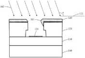
本申请实施例的一方面,提供一种半导体器件制备方法,方法包括:在半导体层上形成具有第一窗口的光刻胶层;在第一窗口内的半导体层上蒸镀形成关键层金属;在光刻胶层上通过倾角蒸镀形成具有第二窗口的第一介质层,第二窗口位于第一窗口的正上方且与第一窗口连通形成第三窗口,第二窗口的开窗面积小于第一窗口的开窗面积;在第三窗口内的关键层金属上蒸镀形成第一上层金属以得到叠层金属,其中,叠层金属具有相对的第一侧和第二侧,第一上层金属和关键层金属位于第一侧的两边缘和/或第二侧的两边缘之间具有第一预设间距。In one aspect of the embodiments of the present application, a method for fabricating a semiconductor device is provided. The method includes: forming a photoresist layer with a first window on a semiconductor layer; forming a key layer metal by vapor deposition on the semiconductor layer in the first window; A first dielectric layer with a second window is formed on the photoresist layer by tilt angle evaporation, the second window is located directly above the first window and communicates with the first window to form a third window, and the opening area of the second window is less than The opening area of the first window; the first upper layer metal is formed by vapor deposition on the key layer metal in the third window to obtain a laminated metal, wherein the laminated metal has opposite first and second sides, and the first upper layer The metal and the metal of the key layer are located at a first predetermined distance between the two edges of the first side and/or the two edges of the second side.
可选的,在第三窗口内的关键层金属上蒸镀形成第一上层金属以得到叠层金属之后,方法还包括:在第一介质层上通过倾角蒸镀形成具有第四窗口的第二介质层,第四窗口位于第二窗口的正上方且与第三窗口连通形成第五窗口,第四窗口的开窗面积小于第二窗口的开窗面积;在第五窗口内的第一上层金属上蒸镀形成第二上层金属,第二上层金属和第一上层金属位于第一侧的两边缘和/或第二侧的两边缘之间具有第二预设间距。Optionally, after forming the first upper layer metal by vapor deposition on the key layer metal in the third window to obtain the laminated metal, the method further includes: forming a second layer having a fourth window on the first dielectric layer by dip angle evaporation. In the dielectric layer, the fourth window is located directly above the second window and communicates with the third window to form a fifth window, and the opening area of the fourth window is smaller than that of the second window; the first upper metal layer in the fifth window The second upper layer metal is formed by upper evaporation, and the second upper layer metal and the first upper layer metal are located at the two edges of the first side and/or the two edges of the second side with a second predetermined distance.
可选的,第一预设间距和/或第二预设间距为0.07μm至0.1μm。Optionally, the first preset spacing and/or the second preset spacing is 0.07 μm to 0.1 μm.
可选的,第一介质层包括层叠的第一子层和第二子层,在光刻胶层上通过倾角蒸镀形成具有第二窗口的第一介质层包括:在光刻胶层上通过第一次倾角蒸镀形成具有窗口的第一子层;在第一子层上通过第二次倾角蒸镀形成具有窗口的第二子层,第一子层的窗口与第二子层的窗口连通形成第二窗口,第一次倾角蒸镀的原子入射方向沿顺时针方向转动至水平方向所需的角度为钝角,第二次倾角蒸镀的原子入射方向沿顺时针方向转动至水平方向所需的角度为锐角。Optionally, the first dielectric layer includes a stacked first sub-layer and a second sub-layer, and forming the first dielectric layer with the second window by tilting evaporation on the photoresist layer includes: passing on the photoresist layer A first sublayer with windows is formed by the first dip angle evaporation; a second sublayer with windows is formed on the first sublayer by the second dip angle evaporation, and the windows of the first sublayer and the windows of the second sublayer are formed. Connected to form a second window, the angle required for the atomic incident direction of the first dip angle evaporation to rotate clockwise to the horizontal direction is an obtuse angle, and the atomic incident direction of the second dip angle evaporation to rotate clockwise to the horizontal direction. The required angle is an acute angle.
可选的,第一次倾角蒸镀的原子入射方向和/或第二次倾角蒸镀的原子入射方向与半导体层厚度方向的夹角为10°至20°。Optionally, the included angle between the atomic incident direction of the first dip angle evaporation and/or the atomic incident direction of the second dip angle evaporation and the thickness direction of the semiconductor layer is 10° to 20°.
可选的, 在第一窗口内的半导体层上蒸镀形成关键层金属包括:在第一窗口内的半导体层上沿平行半导体层厚度方向蒸镀形成关键层金属。Optionally, forming the key layer metal by vapor deposition on the semiconductor layer in the first window includes: forming the key layer metal by vapor deposition on the semiconductor layer in the first window along a thickness direction parallel to the semiconductor layer.
可选的,在第三窗口内的关键层金属上蒸镀形成第一上层金属包括:在第三窗口内的关键层金属上沿平行半导体层厚度方向蒸镀形成第一上层金属。Optionally, forming the first upper layer metal by vapor deposition on the key layer metal in the third window includes: forming the first upper layer metal by vapor deposition on the key layer metal in the third window along a thickness direction parallel to the semiconductor layer.
本申请实施例的另一方面,提供一种半导体器件,包括半导体层和设置于半导体层上的叠层金属,叠层金属包括依次设置于半导体层上的关键层金属和第一上层金属,叠层金属具有相对的第一侧和第二侧,第一上层金属在半导体层的正投影位于关键层金属在半导体层的正投影内,且第一上层金属和关键层金属位于第一侧的两边缘和/或第二侧的两边缘之间具有第一预设间距。In another aspect of the embodiments of the present application, a semiconductor device is provided, which includes a semiconductor layer and a laminated metal disposed on the semiconductor layer. The laminated metal includes a key layer metal and a first upper layer metal disposed on the semiconductor layer in sequence. The layer metal has opposing first and second sides, the orthographic projection of the first upper metal layer on the semiconductor layer is within the orthographic projection of the key layer metal on the semiconductor layer, and the first upper layer metal and the critical layer metal are located on opposite sides of the first side. There is a first predetermined distance between the edge and/or the two edges of the second side.
可选的,半导体器件还包括设置于第一上层金属上的第二上层金属,第二上层金属在半导体层的正投影位于第一上层金属在半导体层的正投影内,且第二上层金属和第一上层金属位于第一侧的两边缘和/或第二侧的两边缘之间具有第二预设间距。Optionally, the semiconductor device further includes a second upper layer metal disposed on the first upper layer metal, the orthographic projection of the second upper layer metal on the semiconductor layer is located in the orthographic projection of the first upper layer metal on the semiconductor layer, and the second upper layer metal and There is a second predetermined distance between the two edges of the first upper layer metal on the first side and/or the two edges of the second side.
可选的,第一预设间距和/或第二预设间距为0.07μm至0.1μm。Optionally, the first preset spacing and/or the second preset spacing is 0.07 μm to 0.1 μm.
本申请的有益效果包括:The beneficial effects of this application include:
本申请提供了一种半导体器件及其制备方法,方法包括:在半导体层上形成具有第一窗口的光刻胶层;在第一窗口内的半导体层上蒸镀形成关键层金属;在光刻胶层上通过倾角蒸镀形成具有第二窗口的第一介质层,第二窗口位于第一窗口的正上方且与第一窗口连通形成第三窗口,第二窗口的开窗面积小于第一窗口的开窗面积;在第三窗口内的关键层金属上蒸镀形成第一上层金属,使得第一上层金属与关键层金属的相对两侧的边缘之间具有第一预设间距。如此,在欧姆金属的合金化过程中,由于位于第一预设间距范围内的关键层金属上方无其它层金属,可以使得关键层金属的边缘与半导体层能够充分进行合金化,提高合金反应效率,从而有效降低欧姆接触的电阻,尤其对于氮化镓基器件来讲,欧姆接触最有效导通电流的区域局限在欧姆金属与氮化镓界面的边缘部分,因此,通过上述方法能够进一步降低其欧姆接触的电阻,使得欧姆金属具有较高的电导率。此外,在欧姆金属退火后,还可以使得欧姆金属的边缘起伏较小,较为平整,从而提高器件栅源和栅漏之间的可靠性,增强器件的耐击穿能力。The application provides a semiconductor device and a preparation method thereof. The method includes: forming a photoresist layer with a first window on the semiconductor layer; forming a key layer metal by vapor deposition on the semiconductor layer in the first window; A first dielectric layer with a second window is formed on the adhesive layer by dip angle evaporation, the second window is located directly above the first window and communicates with the first window to form a third window, and the opening area of the second window is smaller than that of the first window A first upper layer metal is formed by vapor deposition on the key layer metal in the third window, so that there is a first preset distance between the first upper layer metal and the edges on opposite sides of the key layer metal. In this way, during the alloying process of the ohmic metal, since there is no other metal layer above the key layer metal within the first preset spacing range, the edge of the key layer metal and the semiconductor layer can be fully alloyed, and the alloying reaction efficiency can be improved. , so as to effectively reduce the resistance of the ohmic contact, especially for GaN-based devices, the most effective conduction current region of the ohmic contact is limited to the edge portion of the interface between the ohmic metal and the gallium nitride. Therefore, the above method can further reduce its resistance. The resistance of the ohmic contact makes the ohmic metal have a higher conductivity. In addition, after the ohmic metal is annealed, the edge of the ohmic metal can be made smaller and flatter, thereby improving the reliability between the gate-source and the gate-drain of the device and enhancing the breakdown resistance of the device.
附图说明Description of drawings
为了更清楚地说明本申请实施例的技术方案,下面将对实施例中所需要使用的附图作简单地介绍,应当理解,以下附图仅示出了本申请的某些实施例,因此不应被看作是对范围的限定,对于本领域普通技术人员来讲,在不付出创造性劳动的前提下,还可以根据这些附图获得其他相关的附图。In order to illustrate the technical solutions of the embodiments of the present application more clearly, the following drawings will briefly introduce the drawings that need to be used in the embodiments. It should be understood that the following drawings only show some embodiments of the present application, and therefore do not It should be regarded as a limitation of the scope, and for those of ordinary skill in the art, other related drawings can also be obtained according to these drawings without any creative effort.
图1为本申请实施例提供的一种半导体器件制备方法的流程示意图;1 is a schematic flowchart of a method for fabricating a semiconductor device according to an embodiment of the present application;
图2为本申请实施例提供的一种半导体器件的制备状态示意图之一;FIG. 2 is one of the schematic diagrams of the preparation state of a semiconductor device provided by an embodiment of the present application;
图3为本申请实施例提供的一种半导体器件的制备状态示意图之二;FIG. 3 is the second schematic diagram of the preparation state of a semiconductor device provided by the embodiment of the present application;
图4为本申请实施例提供的一种半导体器件的制备状态示意图之三;FIG. 4 is the third schematic diagram of the preparation state of a semiconductor device provided by the embodiment of the present application;
图5为本申请实施例提供的一种半导体器件的制备状态示意图之四;FIG. 5 is the fourth schematic diagram of the preparation state of a semiconductor device provided by the embodiment of the present application;
图6为本申请实施例提供的一种半导体器件的制备状态示意图之五;FIG. 6 is the fifth schematic diagram of the preparation state of a semiconductor device provided by the embodiment of the present application;
图7为本申请实施例提供的一种半导体器件的结构示意图;FIG. 7 is a schematic structural diagram of a semiconductor device provided by an embodiment of the present application;
图8为本申请实施例提供的欧姆金属的结构示意图之一;FIG. 8 is one of the schematic structural diagrams of the ohmic metal provided by the embodiment of the present application;
图9为本申请实施例提供的欧姆金属的结构示意图之二;FIG. 9 is the second schematic diagram of the structure of the ohmic metal provided by the embodiment of the present application;
图10为现有技术提供的退火后的欧姆金属的俯视图;10 is a top view of the annealed ohmic metal provided by the prior art;
图11为本申请实施例提供的退火后的欧姆金属的俯视图。FIG. 11 is a top view of the annealed ohmic metal according to an embodiment of the present application.
图标:100-衬底;110-半导体层;111-水平方向;120-光刻胶层;121-第一窗口;130-关键层金属;131-关键层金属蒸镀的原子入射方向;140-第一子层;141-第一延伸部;142-第一次倾角蒸镀的原子入射方向;150-第二子层;151-第二延伸部;152-第二次倾角蒸镀的原子入射方向;160-第一介质层;161-第二窗口;170-第一上层金属;171-第一上层金属蒸镀的原子入射方向;180-第二上层金属。Icon: 100-substrate; 110-semiconductor layer; 111-horizontal direction; 120-photoresist layer; 121-first window; The first sublayer; 141 - the first extension; 142 - the atomic incidence direction of the first dip angle evaporation; 150 - the second sublayer; 151 - the second extension part; 152 - the atomic incidence of the second dip angle evaporation 160-the first dielectric layer; 161-the second window; 170-the first upper metal layer; 171-the atomic incident direction of the vapor deposition of the first upper layer metal; 180-the second upper layer metal.
具体实施方式Detailed ways
下文陈述的实施方式表示使得本领域技术人员能够实践所述实施方式所必需的信息,并且示出了实践所述实施方式的最佳模式。在参照附图阅读以下描述之后,本领域技术人员将了解本公开的概念,并且将认识到本文中未具体提出的这些概念的应用。应理解,这些概念和应用属于本公开和随附权利要求的范围内。The embodiments set forth below represent the necessary information to enable those skilled in the art to practice the embodiments, and illustrate the best mode for practicing the embodiments. After reading the following description with reference to the accompanying drawings, those skilled in the art will appreciate the concepts of the present disclosure and will recognize applications of these concepts not specifically set forth herein. It should be understood that these concepts and applications are within the scope of the present disclosure and appended claims.
应当理解,虽然术语第一、第二等可以在本文中用于描述各种元件,但是这些元件不应受这些术语的限制。这些术语仅用于区分一个元件与另一个元件。例如,在不脱离本公开的范围的情况下,第一元件可称为第二元件,并且类似地,第二元件可称为第一元件。如本文所使用,术语“和/或”包括相关联的所列项中的一个或多个的任何和所有组合。It will be understood that, although the terms first, second, etc. may be used herein to describe various elements, these elements should not be limited by these terms. These terms are only used to distinguish one element from another. For example, a first element could be termed a second element, and, similarly, a second element could be termed a first element, without departing from the scope of the present disclosure. As used herein, the term "and/or" includes any and all combinations of one or more of the associated listed items.
应当理解,当一个元件(诸如层、区域或衬底)被称为“在另一个元件上”或“延伸到另一个元件上”时,其可以直接在另一个元件上或直接延伸到另一个元件上,或者也可以存在介于中间的元件。相反,当一个元件被称为“直接在另一个元件上”或“直接延伸到另一个元件上”时,不存在介于中间的元件。同样,应当理解,当元件(诸如层、区域或衬底)被称为“在另一个元件之上”或“在另一个元件之上延伸”时,其可以直接在另一个元件之上或直接在另一个元件之上延伸,或者也可以存在介于中间的元件。相反,当一个元件被称为“直接在另一个元件之上”或“直接在另一个元件之上延伸”时,不存在介于中间的元件。还应当理解,当一个元件被称为“连接”或“耦接”到另一个元件时,其可以直接连接或耦接到另一个元件,或者可以存在介于中间的元件。相反,当一个元件被称为“直接连接”或“直接耦接”到另一个元件时,不存在介于中间的元件。It will be understood that when an element such as a layer, region or substrate is referred to as being "on" or "extending on" another element, it can be directly on or extending directly to the other element elements, or intervening elements may also be present. In contrast, when an element is referred to as being "directly on" or "extending directly onto" another element, there are no intervening elements present. Also, it will be understood that when an element such as a layer, region or substrate is referred to as being "on" or "extending over" another element, it can be directly on or directly on the other element Extends over another element, or intervening elements may also be present. In contrast, when an element is referred to as being "directly on" or "extending directly on" another element, there are no intervening elements present. It will also be understood that when an element is referred to as being "connected" or "coupled" to another element, it can be directly connected or coupled to the other element or intervening elements may be present. In contrast, when an element is referred to as being "directly connected" or "directly coupled" to another element, there are no intervening elements present.
诸如“在…下方”或“在…上方”或“上部”或“下部”或“水平”或“垂直”的相关术语在本文中可用来描述一个元件、层或区域与另一个元件、层或区域的关系,如图中所示出。应当理解,这些术语和上文所论述的那些术语意图涵盖装置的除图中所描绘的取向之外的不同取向。Relative terms such as "below" or "above" or "upper" or "lower" or "horizontal" or "vertical" may be used herein to describe one element, layer or region in relation to another element, layer or region. The relationship of the regions is shown in the figure. It should be understood that these terms and those discussed above are intended to encompass different orientations of the device in addition to the orientation depicted in the figures.
本文中使用的术语仅用于描述特定实施方式的目的,而且并不意图限制本公开。如本文所使用,除非上下文明确地指出,否则单数形式“一”、“一个”和“所述”意图同样包括复数形式。还应当理解,当在本文中使用时,术语“包括”指明存在所述特征、整数、步骤、操作、元件和/或部件,但并不排除存在或者增添一个或多个其他特征、整数、步骤、操作、元件、部件和/或上述各项的组。The terminology used herein is for the purpose of describing particular embodiments only and is not intended to limit the present disclosure. As used herein, the singular forms "a," "an," and "the" are intended to include the plural forms as well, unless the context clearly dictates otherwise. It should also be understood that, when used herein, the term "comprising" indicates the presence of stated features, integers, steps, operations, elements and/or components, but does not preclude the presence or addition of one or more other features, integers, steps , operations, elements, components and/or groups of the foregoing.
除非另外定义,否则本文中使用的所有术语(包括技术术语和科学术语)的含义与本公开所属领域的普通技术人员通常理解的含义相同。还应当理解,本文所使用的术语应解释为含义与它们在本说明书和相关领域的情况下的含义一致,而不能以理想化或者过度正式的意义进行解释,除非本文中已明确这样定义。Unless otherwise defined, all terms (including technical and scientific terms) used herein have the same meaning as commonly understood by one of ordinary skill in the art to which this disclosure belongs. It is also to be understood that terms used herein should be construed to have the same meaning as they have in the context of this specification and related art, and not to be construed in an idealized or overly formal sense unless explicitly defined as such herein.
本申请实施例的一方面,提供一种半导体器件制备方法,如图1所示,方法包括:In one aspect of the embodiments of the present application, a method for fabricating a semiconductor device is provided, as shown in FIG. 1 , the method includes:
S010:在半导体层上形成具有第一窗口的光刻胶层。S010: forming a photoresist layer with a first window on the semiconductor layer.
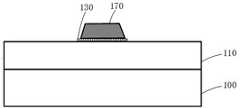
如图2所示,在半导体层110上涂覆整层光刻胶,然后通过曝光、显影等工艺在其上形成第一窗口121,使得位于光刻胶层120下方的半导体层110在第一窗口121内露出,从而作为后续与欧姆金属接触的区域。As shown in FIG. 2, a whole layer of photoresist is coated on the
半导体层110可以是单层或叠层,具体设置时,可以根据器件类型进行合理选择,例如根据绝缘栅型场效应晶体管(MIS FET)、高电子迁移率晶体管(HEMT)等进行选择,本申请不对其做限制。The
请继续参照图2所示,光刻胶层120可以包括叠层结构,例如包括下层的剥离胶和上层的感光胶,如此,即便于后续对光刻胶层120的剥离,也便于实现第一窗口121的形成。此外,光刻胶层120也可以为一般的光刻胶层120,在对其进行图形化时,可以使得曝光后形成倒梯形结构。Please continue to refer to FIG. 2 , the
如图2所示,在半导体层110的底面还可以设置有衬底100,该衬底100可以是用于承载半导体集成电路元器件的基材,例如GaN、GaAs、SiC等。然后在该衬底100上沉积半导体层110,沉积的方式可以是通过化学气相沉积(CVD)、物理气相沉积(PVD)或原子层沉积(ALD)等工艺进行,本申请对其不做限定,具体可以根据实际需求进行合理选择。As shown in FIG. 2 , a
S020:在第一窗口内的半导体层上蒸镀形成关键层金属。S020: Evaporating to form a key layer metal on the semiconductor layer in the first window.
如图3所示,继续在半导体层110上蒸镀金属,由于光刻胶层120的遮挡,因此,蒸镀的金属分布于第一窗口121内露出的半导体层110的表面和光刻胶层120,其中,位于第一窗口121内的半导体层110上的金属作为关键层金属130,其与半导体层110表面直接接触。As shown in FIG. 3 , the metal is continuously evaporated on the
S030:在光刻胶层上通过倾角蒸镀形成具有第二窗口的第一介质层,第二窗口位于第一窗口的正上方且与第一窗口连通形成第三窗口,第二窗口的面积小于第一窗口的面积。S030 : forming a first dielectric layer with a second window on the photoresist layer by tilt angle evaporation, the second window is located directly above the first window and communicates with the first window to form a third window, and the area of the second window is less than The area of the first window.
如图5所示,在形成有关键层金属130后,继续在具有第一窗口121的光刻胶层120上方采用倾角蒸镀形成具有第二窗口161的第一介质层160,并且第二窗口161位于第一窗口121的正上方,第二窗口161与第一窗口121连通一起形成第三窗口,关键层金属130在第三窗口内露出,即在进行蒸镀时,使得原子入射方向不再是一般的竖直方向,而是倾斜一定角度入射,如此,能够使得第一介质层160在覆盖光刻胶层120上的金属(该部分金属与制作关键层金属130时同步形成于光刻胶层120上表面)的基础上,也能够在第一窗口121的侧壁形成向第一窗口121中心延伸的延伸部,即位于第一介质层160上的第二窗口161由延伸部围绕形成,借由延伸部能够使得第一窗口121上方的第二窗口161的开窗面积内缩变小,换言之,第二窗口161的面积小于第一窗口121的面积。As shown in FIG. 5 , after the
S040:在第三窗口内的关键层金属上蒸镀形成第一上层金属以得到叠层金属,其中,叠层金属具有相对的第一侧和第二侧,第一上层金属和关键层金属位于第一侧的两边缘和/或第二侧的两边缘之间具有第一预设间距。S040: Evaporating to form a first upper layer metal on the key layer metal in the third window to obtain a laminated metal, wherein the laminated metal has opposite first and second sides, and the first upper metal and the key layer metal are located at There is a first predetermined distance between the two edges of the first side and/or the two edges of the second side.
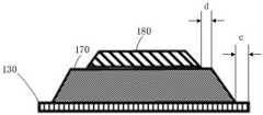
如图6和图8所示,在形成有第一介质层160后,继续蒸镀金属,由于第一介质层160的遮挡和关键层金属130在第三窗口的露出,因此,蒸镀的金属分布于第一介质层160的表面和第三窗口内露出的关键层金属130表面,其中,位于关键层金属130上的金属作为第一上层金属170,其与关键层金属130表面直接接触,两者一起作为叠层金属,叠层金属具有相对的第一侧和第二侧,为便于后续描述,如图6至图8所示,第一侧为左侧,第二侧为右侧。在本实施例中,欧姆金属包括叠层金属。As shown in FIG. 6 and FIG. 8 , after the
由于第三窗口中位于上层的第二窗口161的开窗面积相对位于下层的第一窗口121的开窗面积缩小,使得形成于关键层金属130上的第一上层金属170在左右两侧相对关键层金属130向内收缩,在左右两侧形成阶梯状,换言之,第一上层金属170不仅位于关键层金属130的正上方,而且第一上层金属170在半导体层110的正投影的面积小于关键层金属130在半导体层110的正投影的面积,并且满足第一上层金属170与关键层金属130在左侧的两边缘之间具有第一预设间距c,在右侧的两边缘之间具有第一预设间距c。当然,在其它实施方式中,还可以是第一上层金属170与关键层金属130仅在左侧的两边缘之间具有第一预设间距c;或,还可以是第一上层金属170与关键层金属130仅在右侧的两边缘之间具有第一预设间距c。Since the opening area of the
如此,在欧姆金属的合金化过程中,由于位于第一预设间距c范围内的关键层金属130上方无其它层金属,可以使得关键层金属130的边缘与半导体层110能够充分进行合金化,提高合金反应效率,从而有效降低欧姆接触的电阻,尤其对于氮化镓基器件来讲,欧姆接触最有效导通电流的区域局限在欧姆金属与氮化镓界面的边缘部分,因此,通过上述方法能够进一步降低其欧姆接触的电阻,使得欧姆金属具有较高的电导率。In this way, during the alloying process of the ohmic metal, since there is no other metal layer above the
此外,如图10所示,示出了现有的欧姆金属500在退火后,由于不同金属的熔点和扩散能力不同,导致欧姆金属的边缘呈现明显的起伏,使得栅源、栅漏的距离不一致,造成了击穿薄弱点集中在退火后欧姆金属突出最大处,易发生电压击穿风险。In addition, as shown in FIG. 10 , after annealing of the existing
如图11所示,本申请中的欧姆金属190在退火后,由于位于第一预设间距c范围内的关键层金属130上方无其它层金属,因此,欧姆金属的边缘起伏较小,较为平整,使得栅源、栅漏的距离一致性较高,提高器件栅源和栅漏之间的可靠性,增强器件的耐击穿能力。As shown in FIG. 11 , after the
在一些实施方式中,对欧姆金属进行退火时,退火温度650到750℃,退火时间30s到100s,在N2气氛中进行。In some embodiments, when annealing the ohmic metal, the annealing temperature is 650 to 750° C., the annealing time is 30 s to 100 s, and the annealing is performed in a N2 atmosphere.
在一些实施方式中,光刻胶层120的厚度为1.1μm至1.5μm。In some embodiments, the thickness of the
在一些实施方式中,关键层金属130的材质为Si/Ti、Ta/Si、Ti/Si/Ti等低功函数金属组合;关键层金属130的厚度可以根据具体的需求灵活设置,例如当关键层金属130的材质为Si/Ti时,厚度对应为30 Å/50 Å;当关键层金属130的材质为Ti/Si/Ti时,厚度对应为10 Å/30 Å/50 Å。In some embodiments, the material of the
在一些实施方式中,第一介质层160的材质为Al、Au或SiO2等,第一介质层160的厚度可以根据具体需求灵活设置,例如当第一介质层160的材质为Al时,厚度为1000 Å至1500Å。In some embodiments, the material of the
如图7所示,在形成有第一上层金属170后,可以通过剥离的方式去除光刻胶层120,保留窗口内的欧姆金属。As shown in FIG. 7 , after the first
可选的,在第三窗口内的关键层金属130上蒸镀形成第一上层金属170以得到叠层金属之后,方法还包括:继续在第一上层金属170上形成第二上层金属180,以此利用第二上层金属180的特性使得欧姆金属整体形成较佳的性能,第二上层金属180的形成可以参照第一上层金属170的形成,具体的,如下:Optionally, after forming the first
在形成有第一上层金属170后,继续在具有第二窗口161的第一介质层160上方采用倾角蒸镀形成具有第四窗口的第二介质层,并且第四窗口位于第二窗口161或第三窗口的正上方,第四窗口与第三窗口连通一起形成第五窗口(即第一窗口121、第二窗口161和第四窗口一起连通形成第五窗口),即在进行蒸镀时,使得原子入射方向不再是一般的竖直方向,而是倾斜一定角度入射,如此,能够使得第二介质层在覆盖第一介质层160上金属(如前所述,该部分金属与制作第一上层金属170时同步形成于第一介质层160上表面)的基础上,也能够在第三窗口的侧壁形成向第三窗口中心延伸的延伸部,即位于第二介质层上的第四窗口由延伸部围绕形成,借由延伸部能够使得第三窗口上方的第四窗口的开窗面积继续内缩变小,换言之,第四窗口的面积小于第二窗口161的面积。After the first
如图9所示,在形成有第二介质层后,继续蒸镀金属,在第五窗口内露出的第一上层金属170上形成与第一上层金属170表面直接接触的第二上层金属180,第二上层金属180也在第一侧和第二侧具有边缘,故,第二上层金属180与第一上层金属170位于第一侧的两边缘和/或第二侧的两边缘之间具有第二预设间距d,使得各层金属的边缘之间相互分离,以进一步加强欧姆金属退火后形貌改善。在本实施例中,欧姆金属包括层叠的关键层金属130、第一上层金属170和第二上层金属180。应当理解的是,本实施例包括第二上层金属180与第一上层金属170位于第一侧的两边缘之间具有第二预设间距d;第二上层金属180与第一上层金属170位于第二侧的两边缘之间具有第二预设间距d;第二上层金属180与第一上层金属170位于第一侧的两边缘和第二侧的两边缘之间各自均具有第二预设间距d的三种情况。As shown in FIG. 9 , after the second dielectric layer is formed, metal deposition is continued, and a second
在一些实施方式中,第一上层金属170可以是高电导率金属。在一些实施方式中,第二上层金属180可以是抗氧化层金属。例如第一上层金属170/第二上层金属180可以是Al/Au。此外,还可以在第一上层金属170和第二上层金属180之间设置阻挡层金属,例如Ni,以使得欧姆金属具有较佳的性能,当是Al/Ni/Au时,对应的三者厚度可以是1400 Å/550 Å/450 Å。In some embodiments, the first
可选的,如图8所示,第一预设间距为0.07μm至0.1μm,如此,既能够降低欧姆接触的电阻,改善退火形貌的同时,还能够保证整个欧姆金属整体的性能。Optionally, as shown in FIG. 8 , the first preset spacing is 0.07 μm to 0.1 μm, which can not only reduce the resistance of the ohmic contact, improve the annealing morphology, but also ensure the overall performance of the entire ohmic metal.
可选的,如图9所示,第二预设间距为0.07μm至0.1μm,如此,既能够改善退火形貌的同时,还能够保证整个欧姆金属整体的性能。Optionally, as shown in FIG. 9 , the second preset spacing is 0.07 μm to 0.1 μm, which can not only improve the annealing morphology, but also ensure the overall performance of the entire ohmic metal.
应当理解的是,一方面本申请中的欧姆金属还可以包括第三上层金属、第四上层金属等等,其形成方式均可以对应参照前述第一上层金属170和第二上层金属180,在此不再赘述。另一方面,本申请中的第一预设间距和第二预设间距均代表蒸镀后、退火前,各层金属相对两侧边缘之间的间距。It should be understood that, on the one hand, the ohmic metal in the present application may also include a third upper layer metal, a fourth upper layer metal, etc., and the formation methods thereof can be referred to the aforementioned first
可选的,第一介质层160包括层叠的第一子层140和第二子层150,对应的第二介质层也可以包括层叠的第三子层和第四子层,第一介质层160的制备过程和第二介质层的制备过程相似,以下以第一介质层160为例进行说明:Optionally, the
通过S030在光刻胶层120上通过倾角蒸镀形成具有第二窗口161的第一介质层160包括:Forming the
如图4所示,首先在光刻胶层120上通过第一次倾角蒸镀形成具有窗口的第一子层140,在进行第一次倾角蒸镀时,控制第一次倾角蒸镀的原子入射方向142沿顺时针方向转动至水平方向111所需的角度a为钝角,如此,能够使得第一子层140在形成时更多的覆盖到第一窗口121的右侧壁,从而在第一窗口121右侧壁形成朝向第一窗口121中心延伸的第一延伸部141。As shown in FIG. 4 , firstly, a
如图5所示,接着在第一子层140上通过第二次倾角蒸镀形成具有窗口的第二子层150,第一子层140的窗口与第二子层150的窗口连通形成第二窗口161,在进行第二次倾角蒸镀时,控制第二次倾角蒸镀的原子入射方向152沿顺时针方向转动至水平方向111所需的角度b为锐角,如此,能够使得第二子层150在形成时更多的覆盖到第一窗口121的左侧壁,从而在第一窗口121左侧壁形成朝向第一窗口121中心延伸的第二延伸部151。As shown in FIG. 5 , a
如此,能够使得第二窗口161位于第一窗口121的正上方,且第二窗口161的开窗面积相对第一窗口121的开窗面积进行内缩,如此,便可以通过控制调整第二窗口161的窗口面积,精确控制第一上层金属170相对关键层金属130的第一预设间距c的大小。In this way, the
可选的,第一次倾角蒸镀的原子入射方向142与半导体层110厚度方向的夹角为10°至20°,换言之,如图4所示,第一次倾角蒸镀的原子入射方向142沿顺时针方向转动至水平方向111所需的角度a为钝角,该钝角为100°至110°。Optionally, the included angle between the
可选的,第二次倾角蒸镀的原子入射方向152与半导体层110厚度方向的夹角为10°至20°,换言之,如图5所示,第二次倾角蒸镀的原子入射方向152沿顺时针方向转动至水平方向111所需的角度b为锐角,该锐角为70°至80°。Optionally, the included angle between the
在一些实施方式中,第一次倾角蒸镀的原子入射方向142与水平方向111的角度a和第二次倾角蒸镀的原子入射方向152与水平方向111的角度b可以互补。In some embodiments, the angle a between the
可选的,如图3所示,通过S020在第一窗口121内的半导体层110上蒸镀形成关键层金属130时,可以使得关键层金属蒸镀的原子入射方向131与半导体层110厚度方向平行,蒸镀形成关键层金属130。Optionally, as shown in FIG. 3 , when the
可选的,如图6所示,通过S040在第三窗口内的关键层金属130上蒸镀形成第一上层金属170时,可以使得第一上层金属蒸镀的原子入射方向171与半导体层110厚度方向平行,蒸镀形成第一上层金属170。Optionally, as shown in FIG. 6 , when the first
本申请实施例的另一方面,提供一种半导体器件,如图7所示,包括半导体层110和设置于半导体层110上的叠层金属,叠层金属包括依次设置于半导体层110上的关键层金属130和第一上层金属170,其中,叠层金属具有相对的第一侧和第二侧,如图8所示,形成于关键层金属130上的第一上层金属170在第一侧和/或第二侧相对关键层金属130向内收缩,两者配合形成阶梯状,换言之,第一上层金属170在半导体层110的正投影位于关键层金属130在半导体层110的正投影内,且第一上层金属170和关键层金属130位于第一侧的两边缘和/或第二侧的两边缘之间具有第一预设间距c,如此,在欧姆金属的合金化过程中,由于位于第一预设间距c范围内的关键层金属130上方无其它层金属,可以使得关键层金属130的边缘与半导体层110能够充分进行合金化,从而有效降低欧姆接触的电阻,尤其对于氮化镓基器件来讲,欧姆接触最有效导通电流的区域局限在欧姆金属与氮化镓界面的边缘部分,因此,通过上述方法能够进一步降低其欧姆接触的电阻,使得欧姆金属具有较高的电导率。In another aspect of the embodiments of the present application, a semiconductor device is provided, as shown in FIG. 7 , including a
此外,如图11所示,本申请中的欧姆金属190在退火后,由于位于第一预设间距c范围内的关键层金属130上方无其它层金属,因此,欧姆金属的边缘起伏较小,较为平整,使得栅源、栅漏的距离一致性较高,提高器件栅源和栅漏之间的可靠性,增强器件的耐击穿能力。In addition, as shown in FIG. 11 , after annealing of the
可选的,如图9所示,半导体器件还包括设置于第一上层金属170上的第二上层金属180,第二上层金属180也具有位于第一侧和第二侧的边缘,形成于第一上层金属170上的第二上层金属180相对第一上层金属170向内收缩,两者配合形成阶梯状,换言之,第二上层金属180在半导体层110的正投影位于第一上层金属170在半导体层110的正投影内,且第二上层金属180和第一上层金属170位于第一侧的两边缘和/或第二侧的两边缘之间具有第二预设间距d,以加强欧姆金属退火后形貌改善。Optionally, as shown in FIG. 9 , the semiconductor device further includes a second
可选的,如图8所示,第一预设间距为0.07μm至0.1μm,如此,既能够降低欧姆接触的电阻,改善退火形貌的同时,还能够保证整个欧姆金属整体的性能。Optionally, as shown in FIG. 8 , the first preset spacing is 0.07 μm to 0.1 μm, which can not only reduce the resistance of the ohmic contact, improve the annealing morphology, but also ensure the overall performance of the entire ohmic metal.
可选的,如图9所示,第二预设间距为0.07μm至0.1μm,如此,既能够改善退火形貌的同时,还能够保证整个欧姆金属整体的性能。Optionally, as shown in FIG. 9 , the second preset spacing is 0.07 μm to 0.1 μm, which can not only improve the annealing morphology, but also ensure the overall performance of the entire ohmic metal.
以上所述仅为本申请的优选实施例而已,并不用于限制本申请,对于本领域的技术人员来说,本申请可以有各种更改和变化。凡在本申请的精神和原则之内,所作的任何修改、等同替换、改进等,均应包含在本申请的保护范围之内。The above descriptions are only preferred embodiments of the present application, and are not intended to limit the present application. For those skilled in the art, the present application may have various modifications and changes. Any modification, equivalent replacement, improvement, etc. made within the spirit and principle of this application shall be included within the protection scope of this application.
Claims (10)
Priority Applications (1)
| Application Number | Priority Date | Filing Date | Title |
|---|---|---|---|
| CN202210335552.2ACN114496764B (en) | 2022-04-01 | 2022-04-01 | A kind of semiconductor device and preparation method thereof |
Applications Claiming Priority (1)
| Application Number | Priority Date | Filing Date | Title |
|---|---|---|---|
| CN202210335552.2ACN114496764B (en) | 2022-04-01 | 2022-04-01 | A kind of semiconductor device and preparation method thereof |
Publications (2)
| Publication Number | Publication Date |
|---|---|
| CN114496764A CN114496764A (en) | 2022-05-13 |
| CN114496764Btrue CN114496764B (en) | 2022-07-26 |
Family
ID=81487547
Family Applications (1)
| Application Number | Title | Priority Date | Filing Date |
|---|---|---|---|
| CN202210335552.2AActiveCN114496764B (en) | 2022-04-01 | 2022-04-01 | A kind of semiconductor device and preparation method thereof |
Country Status (1)
| Country | Link |
|---|---|
| CN (1) | CN114496764B (en) |
Citations (1)
| Publication number | Priority date | Publication date | Assignee | Title |
|---|---|---|---|---|
| CN107230617A (en)* | 2016-03-25 | 2017-10-03 | 北京大学 | The preparation method of gallium nitride semiconductor device |
Family Cites Families (7)
| Publication number | Priority date | Publication date | Assignee | Title |
|---|---|---|---|---|
| JP3180466B2 (en)* | 1992-10-08 | 2001-06-25 | 双葉電子工業株式会社 | Field emission device and method of manufacturing the same |
| JP3246137B2 (en)* | 1993-10-25 | 2002-01-15 | 双葉電子工業株式会社 | Field emission cathode and method of manufacturing field emission cathode |
| JP2626558B2 (en)* | 1994-06-13 | 1997-07-02 | 日本電気株式会社 | Manufacturing method of T-type gate electrode |
| US5686737A (en)* | 1994-09-16 | 1997-11-11 | Cree Research, Inc. | Self-aligned field-effect transistor for high frequency applications |
| CN1147923C (en)* | 2001-03-02 | 2004-04-28 | 中国科学院微电子中心 | Process for preparing metal pattern of T-shaped emitter or grid of transistor |
| US9437783B2 (en)* | 2012-05-08 | 2016-09-06 | Cree, Inc. | Light emitting diode (LED) contact structures and process for fabricating the same |
| CN113594038B (en)* | 2021-09-27 | 2022-03-04 | 深圳市时代速信科技有限公司 | Semiconductor device preparation method |
- 2022
- 2022-04-01CNCN202210335552.2Apatent/CN114496764B/enactiveActive
Patent Citations (1)
| Publication number | Priority date | Publication date | Assignee | Title |
|---|---|---|---|---|
| CN107230617A (en)* | 2016-03-25 | 2017-10-03 | 北京大学 | The preparation method of gallium nitride semiconductor device |
Also Published As
| Publication number | Publication date |
|---|---|
| CN114496764A (en) | 2022-05-13 |
Similar Documents
| Publication | Publication Date | Title |
|---|---|---|
| CA2829245C (en) | Systems and methods for ohmic contacts in silicon carbide devices | |
| CN104134689A (en) | HEMT device and manufacturing method thereof | |
| JPS6128232B2 (en) | ||
| JPS5950567A (en) | Manufacture of field effect transistor | |
| CN101572274A (en) | Oxide thin film transistor with etching barrier layer and preparation method thereof | |
| JPS6125227B2 (en) | ||
| TWI737171B (en) | Method of forming a single-crystal hexagonal boron nitride layer and a transistor | |
| CN104103684A (en) | Semiconductor device and manufacturing method | |
| CN210897292U (en) | Gallium nitride epitaxial layer and semiconductor device | |
| CN113437136A (en) | Semiconductor device and preparation method thereof | |
| JP3079851B2 (en) | Method for manufacturing silicon carbide electronic device | |
| WO2015109802A1 (en) | Thin film transistor and manufacturing method thereof, and array substrate | |
| CN113594038B (en) | Semiconductor device preparation method | |
| CN114496764B (en) | A kind of semiconductor device and preparation method thereof | |
| CN102254936B (en) | Compound semiconductor device and method for manufacturing compound semiconductor device | |
| CN113451127B (en) | Power device and preparation method thereof | |
| CN112259604B (en) | Gallium nitride composite substrate, gallium nitride device and preparation method of gallium nitride composite substrate | |
| JP2001036084A (en) | Back metal drain terminal with low stress and thermal resistance | |
| CN107516672B (en) | Schottky contact system suitable for AlGaN/GaN high-electron-mobility transistor | |
| WO2016150075A1 (en) | Thin film transistor, manufacturing method thereof, and array substrate | |
| JP2020102592A (en) | Manufacturing method of semiconductor device | |
| TWI897008B (en) | A method for forming a semiconductor structure | |
| KR102842281B1 (en) | thin film transistor | |
| CN113793869B (en) | An integrated hybrid material high electron mobility transistor and preparation method thereof | |
| CN109037234B (en) | Array substrate and preparation method thereof |
Legal Events
| Date | Code | Title | Description |
|---|---|---|---|
| PB01 | Publication | ||
| PB01 | Publication | ||
| SE01 | Entry into force of request for substantive examination | ||
| SE01 | Entry into force of request for substantive examination | ||
| GR01 | Patent grant | ||
| GR01 | Patent grant |