CN114450809A - Color photoelectric solid-state device - Google Patents
Color photoelectric solid-state deviceDownload PDFInfo
- Publication number
- CN114450809A CN114450809ACN202080068337.XACN202080068337ACN114450809ACN 114450809 ACN114450809 ACN 114450809ACN 202080068337 ACN202080068337 ACN 202080068337ACN 114450809 ACN114450809 ACN 114450809A
- Authority
- CN
- China
- Prior art keywords
- array
- backplane
- microdevice
- microdevices
- vias
- Prior art date
- Legal status (The legal status is an assumption and is not a legal conclusion. Google has not performed a legal analysis and makes no representation as to the accuracy of the status listed.)
- Pending
Links
Images


Classifications
- H—ELECTRICITY
- H10—SEMICONDUCTOR DEVICES; ELECTRIC SOLID-STATE DEVICES NOT OTHERWISE PROVIDED FOR
- H10H—INORGANIC LIGHT-EMITTING SEMICONDUCTOR DEVICES HAVING POTENTIAL BARRIERS
- H10H29/00—Integrated devices, or assemblies of multiple devices, comprising at least one light-emitting semiconductor element covered by group H10H20/00
- H10H29/10—Integrated devices comprising at least one light-emitting semiconductor component covered by group H10H20/00
- H10H29/14—Integrated devices comprising at least one light-emitting semiconductor component covered by group H10H20/00 comprising multiple light-emitting semiconductor components
- H10H29/142—Two-dimensional arrangements, e.g. asymmetric LED layout
- H—ELECTRICITY
- H01—ELECTRIC ELEMENTS
- H01L—SEMICONDUCTOR DEVICES NOT COVERED BY CLASS H10
- H01L25/00—Assemblies consisting of a plurality of semiconductor or other solid state devices
- H01L25/03—Assemblies consisting of a plurality of semiconductor or other solid state devices all the devices being of a type provided for in a single subclass of subclasses H10B, H10D, H10F, H10H, H10K or H10N, e.g. assemblies of rectifier diodes
- H01L25/04—Assemblies consisting of a plurality of semiconductor or other solid state devices all the devices being of a type provided for in a single subclass of subclasses H10B, H10D, H10F, H10H, H10K or H10N, e.g. assemblies of rectifier diodes the devices not having separate containers
- H01L25/075—Assemblies consisting of a plurality of semiconductor or other solid state devices all the devices being of a type provided for in a single subclass of subclasses H10B, H10D, H10F, H10H, H10K or H10N, e.g. assemblies of rectifier diodes the devices not having separate containers the devices being of a type provided for in group H10H20/00
- H01L25/0753—Assemblies consisting of a plurality of semiconductor or other solid state devices all the devices being of a type provided for in a single subclass of subclasses H10B, H10D, H10F, H10H, H10K or H10N, e.g. assemblies of rectifier diodes the devices not having separate containers the devices being of a type provided for in group H10H20/00 the devices being arranged next to each other
- H—ELECTRICITY
- H10—SEMICONDUCTOR DEVICES; ELECTRIC SOLID-STATE DEVICES NOT OTHERWISE PROVIDED FOR
- H10D—INORGANIC ELECTRIC SEMICONDUCTOR DEVICES
- H10D86/00—Integrated devices formed in or on insulating or conducting substrates, e.g. formed in silicon-on-insulator [SOI] substrates or on stainless steel or glass substrates
- H10D86/40—Integrated devices formed in or on insulating or conducting substrates, e.g. formed in silicon-on-insulator [SOI] substrates or on stainless steel or glass substrates characterised by multiple TFTs
- H10D86/441—Interconnections, e.g. scanning lines
- H—ELECTRICITY
- H10—SEMICONDUCTOR DEVICES; ELECTRIC SOLID-STATE DEVICES NOT OTHERWISE PROVIDED FOR
- H10D—INORGANIC ELECTRIC SEMICONDUCTOR DEVICES
- H10D86/00—Integrated devices formed in or on insulating or conducting substrates, e.g. formed in silicon-on-insulator [SOI] substrates or on stainless steel or glass substrates
- H10D86/40—Integrated devices formed in or on insulating or conducting substrates, e.g. formed in silicon-on-insulator [SOI] substrates or on stainless steel or glass substrates characterised by multiple TFTs
- H10D86/451—Integrated devices formed in or on insulating or conducting substrates, e.g. formed in silicon-on-insulator [SOI] substrates or on stainless steel or glass substrates characterised by multiple TFTs characterised by the compositions or shapes of the interlayer dielectrics
- H—ELECTRICITY
- H10—SEMICONDUCTOR DEVICES; ELECTRIC SOLID-STATE DEVICES NOT OTHERWISE PROVIDED FOR
- H10H—INORGANIC LIGHT-EMITTING SEMICONDUCTOR DEVICES HAVING POTENTIAL BARRIERS
- H10H20/00—Individual inorganic light-emitting semiconductor devices having potential barriers, e.g. light-emitting diodes [LED]
- H10H20/80—Constructional details
- H10H20/85—Packages
- H10H20/855—Optical field-shaping means, e.g. lenses
- H10H20/856—Reflecting means
- H—ELECTRICITY
- H10—SEMICONDUCTOR DEVICES; ELECTRIC SOLID-STATE DEVICES NOT OTHERWISE PROVIDED FOR
- H10H—INORGANIC LIGHT-EMITTING SEMICONDUCTOR DEVICES HAVING POTENTIAL BARRIERS
- H10H20/00—Individual inorganic light-emitting semiconductor devices having potential barriers, e.g. light-emitting diodes [LED]
- H10H20/80—Constructional details
- H10H20/85—Packages
- H10H20/857—Interconnections, e.g. lead-frames, bond wires or solder balls
- H—ELECTRICITY
- H10—SEMICONDUCTOR DEVICES; ELECTRIC SOLID-STATE DEVICES NOT OTHERWISE PROVIDED FOR
- H10K—ORGANIC ELECTRIC SOLID-STATE DEVICES
- H10K59/00—Integrated devices, or assemblies of multiple devices, comprising at least one organic light-emitting element covered by group H10K50/00
- H10K59/30—Devices specially adapted for multicolour light emission
- H10K59/35—Devices specially adapted for multicolour light emission comprising red-green-blue [RGB] subpixels
- H10K59/353—Devices specially adapted for multicolour light emission comprising red-green-blue [RGB] subpixels characterised by the geometrical arrangement of the RGB subpixels
- H—ELECTRICITY
- H10—SEMICONDUCTOR DEVICES; ELECTRIC SOLID-STATE DEVICES NOT OTHERWISE PROVIDED FOR
- H10H—INORGANIC LIGHT-EMITTING SEMICONDUCTOR DEVICES HAVING POTENTIAL BARRIERS
- H10H20/00—Individual inorganic light-emitting semiconductor devices having potential barriers, e.g. light-emitting diodes [LED]
- H10H20/80—Constructional details
- H10H20/85—Packages
- H10H20/855—Optical field-shaping means, e.g. lenses
Landscapes
- Engineering & Computer Science (AREA)
- Power Engineering (AREA)
- Microelectronics & Electronic Packaging (AREA)
- Physics & Mathematics (AREA)
- Condensed Matter Physics & Semiconductors (AREA)
- General Physics & Mathematics (AREA)
- Computer Hardware Design (AREA)
- Electroluminescent Light Sources (AREA)
- Mechanical Light Control Or Optical Switches (AREA)
- Led Device Packages (AREA)
Abstract
Description
Translated fromChinese技术领域technical field
本公开涉及光电固态阵列装置,且更特定来说,涉及使用不同微型装置形成微型装置的彩色阵列。The present disclosure relates to optoelectronic solid state array devices, and more particularly, to the use of different microdevices to form color arrays of microdevices.
发明内容SUMMARY OF THE INVENTION
本发明涉及一种具有微型装置的微型装置阵列,其包括:半导体的堆叠层,其接合到背板;所述背板中的垫,其界定子像素,其中多个子像素用于像素阵列中的像素;及所述堆叠层,其接合到所述背板中界定子像素的所述垫。The present invention relates to an array of micro-devices with micro-devices comprising: a stacked layer of semiconductors bonded to a backplane; pads in the backplane that define sub-pixels, wherein a plurality of sub-pixels are used for a pixel; and the stacked layer bonded to the pads in the backplane that define subpixels.
在所述实施例的扩展中,本发明进一步涉及微型装置阵列,其中其为多于一个微型装置阵列的部分。此外,所述微型装置阵列包括第二堆叠层,所述第二堆叠层接合到第一堆叠层的顶部上的背板,其中所述背板中的垫界定子像素。In an extension of the described embodiments, the invention further relates to an array of microdevices, wherein it is part of more than one array of microdevices. Furthermore, the array of microdevices includes a second stack layer bonded to a backplane on top of the first stack layer, wherein the pads in the backplane define subpixels.
在进一步扩展中,第三堆叠层经接合到所述第二堆叠层的顶部上的背板,其中所述背板中的垫界定子像素。In a further extension, a third stack layer is bonded to a backplate on top of the second stack layer, wherein the pads in the backplate define subpixels.
在另一实施例中,本发明公开一种用于在彩色微型装置阵列中调制电阻的方法,所述方法包括:具有每像素多于一个类型的微型装置;在两个相邻像素之间共享至少一个类型的微型装置;及调制所述微型装置的接触层的电阻以产生像素化。In another embodiment, the present invention discloses a method for modulating resistance in a color microdevice array, the method comprising: having more than one type of microdevice per pixel; sharing between two adjacent pixels at least one type of microdevice; and modulating the resistance of a contact layer of the microdevice to produce pixelation.
在另一实施例中,本发明公开一种用于制造彩色微型装置阵列的方法,所述方法包括:在背板的顶部上堆叠单片装置的多于一个层;通过第一垫将第一单片装置接合到所述背板;在所述第一单片装置中形成开口;在所述第一单片装置的所述开口中形成第二垫;及通过所述第二垫将第二单片装置接合到所述背板。In another embodiment, the present invention discloses a method for fabricating an array of colored microdevices, the method comprising: stacking more than one layer of a monolithic device on top of a backplane; A monolithic device is joined to the backplane; an opening is formed in the first monolithic device; a second pad is formed in the opening of the first monolithic device; and a second pad is formed by the second pad A monolithic device is bonded to the backplane.
在另一实施例中,本发明公开用于在彩色微型装置阵列中组合光色彩的方法,所述方法包括:使用线性色彩组合器组合来自不同图像源的光色彩;具有在线性色彩组合器的一个侧上的所述图像源;使用反射器重新引导通过不同图像源产生的光;具有用于图像源的前板以产生或捕获每像素的光;具有用于控制或捕获每像素的所述前板的输出的背板;及将所述图像源耦合到所述线性色彩组合器的少于两个表面。In another embodiment, the present invention discloses a method for combining light colors in an array of color microdevices, the method comprising: combining light colors from different image sources using a linear color combiner; the image source on one side; use a reflector to redirect light generated by different image sources; have a front plate for the image source to generate or capture light per pixel; have the image source for control or capture per pixel a backplane for the output of the frontplane; and less than two surfaces coupling the image source to the linear color combiner.
附图说明Description of drawings
在阅读以下详细描述及参考图式后,本公开的上述及其它优点将变得显而易见。The above and other advantages of the present disclosure will become apparent upon reading the following detailed description and referenced drawings.
图1展示红色微型LED较大的像素结构。Figure 1 shows the larger pixel structure of a red micro LED.
图2展示具有一个共享单片微型装置的像素结构。Figure 2 shows a pixel structure with one shared monolithic microdevice.
图3展示具有多于一个共享单片微型装置的像素结构。3 shows a pixel structure with more than one shared monolithic microdevice.
图4展示用以形成彩色阵列的不同微型装置阵列的堆叠结构。Figure 4 shows a stack structure of different arrays of microdevices used to form a color array.
图5展示使用二向色棱镜以形成彩色显示器的现有方法。Figure 5 shows a prior art method of using dichroic prisms to form a color display.
图6展示使用串行二向色光学件以形成彩色阵列的实施例。6 shows an embodiment using serial dichroic optics to form a color array.
图7展示在串行二向色光学件中使用的个别阵列的俯视图。7 shows a top view of individual arrays used in serial dichroic optics.
图8展示使用不同类型的相同微型装置以形成更好性能彩色阵列的结构。Figure 8 shows a structure using different types of the same microdevice to form a better performing color array.
图9A展示形成为连续像素化的微型装置(阵列)中的一者。FIG. 9A shows one of the microdevices (arrays) formed as successively pixelated.
图9B展示接合到垫的微型装置。Figure 9B shows a microdevice bonded to a pad.
图10A展示形成为连续像素化的微型装置(阵列)中的一者,其具有第二堆叠层上的光学通孔及具有微型装置的凸块。FIG. 10A shows one of the microdevices (arrays) formed as successive pixelation with optical vias on the second stacked layer and bumps with the microdevices.
图10B展示接合到所述背板的图10A中的微型装置。Figure 10B shows the microdevice of Figure 10A bonded to the backplane.
图11A展示具有微型装置阵列的半导体的三个堆叠层。Figure 11A shows three stacked layers of a semiconductor with an array of microdevices.
图11B展示与具有光学通孔的顶层接合在一起的两个堆叠层。Figure 1 IB shows two stacked layers bonded together with a top layer with optical vias.
图11C展示与具有光学通孔的顶层接合在一起的三个堆叠层。Figure 11C shows three stacked layers bonded together with a top layer with optical vias.
虽然本公开易具有各种修改及替代形式,但是特定实施例或实施方案已通过实例在图式中展示,且将在本文中详细描述。然而,应了解,本公开并不希望限于所公开的特定形式。而是,本公开将覆盖落在如由所附权利要求书所界定的本发明的精神及范围内的所有修改例、等效例及替代例。While the present disclosure is susceptible to various modifications and alternative forms, particular embodiments or implementations have been shown by way of example in the drawings and will herein be described in detail. It should be understood, however, that the present disclosure is not intended to be limited to the particular forms disclosed. Rather, this disclosure is to cover all modifications, equivalents, and alternatives falling within the spirit and scope of the invention as defined by the appended claims.
具体实施方式Detailed ways
在本描述中,术语“装置”及“微型装置”是可互换地使用。然而,所属领域的技术人员清楚,此处描述的实施例与装置尺寸无关。In this description, the terms "device" and "microdevice" are used interchangeably. However, as is clear to those skilled in the art, the embodiments described herein are independent of device size.
本公开涉及微型装置阵列,其中所述微型装置阵列可用可靠方法接合到背板。微型装置经制造于微型装置衬底上方。微型装置衬底可包括微型发光二极管(LED)、无机LED、有机LED、传感器、固态装置、集成电路、微电子机械系统(MEMS)及/或其它电子组件。衬底可为装置层的同质衬底,或装置层或固态装置被转移到的接收器衬底。虽然微型LED及显示器可能已被用来解释发明,但相同技术可用于其它应用。The present disclosure relates to arrays of microdevices, wherein the arrays of microdevices can be bonded to a backplane in a reliable manner. Microdevices are fabricated over a microdevice substrate. Microdevice substrates may include microlight emitting diodes (LEDs), inorganic LEDs, organic LEDs, sensors, solid state devices, integrated circuits, microelectromechanical systems (MEMS), and/or other electronic components. The substrate may be a homogenous substrate for the device layer, or a receiver substrate to which the device layer or solid state device is transferred. While micro LEDs and displays may have been used to explain the invention, the same technology can be used for other applications.
背板(或系统)衬底可为任何衬底,且可为刚性或柔性的。背板衬底可由玻璃、硅、塑胶,或任何其它常用材料制成。背板衬底还可具有主动电子组件,例如但不限于晶体管、电阻器、电容器或在系统衬底中常用的任何其它电子组件。在一些情况下,系统衬底可为具有电信号行及列的衬底。背板衬底可为具有电路的背板以导出微型装置。The backplane (or system) substrate can be any substrate and can be rigid or flexible. The backplane substrate can be made of glass, silicon, plastic, or any other commonly used material. The backplane substrate may also have active electronic components such as, but not limited to, transistors, resistors, capacitors, or any other electronic components commonly used in system substrates. In some cases, the system substrate may be a substrate with rows and columns of electrical signals. The backplane substrate may be a backplane with circuitry to derive microdevices.
在大多数微型装置结构中,具有较高波长相关联的装置具有较低性能。在图1中展示的一个实施例中,使用像素结构100,其中与较大波长相关联的微型装置102比其它微型装置104及106更大。In most microdevice configurations, devices with higher wavelengths are associated with lower performance. In one embodiment shown in FIG. 1 , a
在如图2中展示的另一像素结构200-1及200-2中,与其它装置204-1、204-2、206-1及206-2相比,对尺寸减小更敏感的装置202在两个相邻像素之间共享。为产生进一步像素化,装置202经修改以具有个别装置效应202-1及202-2。在一种情况下,通过针对每一子装置202-1及202-2使用两个独立触点来完成修改。此外,我们可修改用于子装置的两个触点之间的经掺杂层的电阻。在倒装芯片结构的情况下,一个共同触点可用于单片装置中的子装置。In another pixel structure 200-1 and 200-2 as shown in FIG. 2, the
如图3中所展示,在通过300-1、300-2、300-3及300-4界定的另一像素结构中,改变像素定向使得相同类型的装置在相同位置中。因此,通过302-1、302-2、304-1、304-2及306-1界定的单片装置可用于相邻像素中的相同装置。为产生进一步像素化,装置302-1、302-2、304-1、304-2、306-1经修改以具有个别装置效应302-1-1到302-1-4、302-2-1到302-2-4、304-1-1到304-1-4、304-2-1到304-2-4、306-1-1到306-1-4。在一种情况下,通过针对每一子装置302-1-1到302-1-4、302-2-1到302-2-4、304-1-1到304-1-4、304-2-1到304-2-4、306-1-1到306-1-4使用两个独立触点来完成修改。此外,我们可修改子装置302-1-1到302-1-4、302-2-1到302-2-4、304-1-1到304-1-4、304-2-1到304-2-4、306-1-1到306-1-4的两个触点之间的经掺杂层的电阻。为减少像素定向变化的效应,可在每一像素的顶部上开发光/彩色漫射器结构。此结构可为透镜或图案化透明层。As shown in FIG. 3, in another pixel structure defined by 300-1, 300-2, 300-3, and 300-4, the pixel orientation is changed so that devices of the same type are in the same location. Thus, a monolithic device defined by 302-1, 302-2, 304-1, 304-2, and 306-1 can be used for the same device in adjacent pixels. To produce further pixelation, devices 302-1, 302-2, 304-1, 304-2, 306-1 are modified to have individual device effects 302-1-1 to 302-1-4, 302-2-1 to 302-2-4, 304-1-1 to 304-1-4, 304-2-1 to 304-2-4, 306-1-1 to 306-1-4. In one case, by for each sub-device 302-1-1 to 302-1-4, 302-2-1 to 302-2-4, 304-1-1 to 304-1-4, 304- 2-1 to 304-2-4, 306-1-1 to 306-1-4 use two independent contacts to complete the modification. In addition, we can modify sub-devices 302-1-1 to 302-1-4, 302-2-1 to 302-2-4, 304-1-1 to 304-1-4, 304-2-1 to 304 - Resistance of the doped layer between the two contacts of 2-4, 306-1-1 to 306-1-4. To reduce the effect of pixel orientation changes, a light/color diffuser structure can be developed on top of each pixel. This structure can be a lens or a patterned transparent layer.
在另一种方法中,单片装置用于多于一个像素,且为实现彩色,不同装置彼此上下堆叠。In another approach, a monolithic device is used for more than one pixel, and different devices are stacked on top of each other to achieve color.
此处,通过调制接触层电阻而使单片装置转变为不同像素化。此外,与用于每一装置的背板上的垫相比,接触层电阻的调制可产生较高分辨率子装置阵列。此实现将装置连接到背板所需的较低对准精度。将第一单片装置(阵列)402转移到衬底(背板或临时或另一单片装置(阵列))。第一单片装置402具有连接垫402-2R,连接垫402-2R将接合到背板上的相应垫。随后,与用于另一装置(阵列)的垫相关联的区域402-4G及402-4B在所述经转移单片装置402(阵列)中敞开。开口402-4G及402-4B经钝化及填充以形成用于下一装置404(阵列)的垫。在敞开之前或之后,或在填充开口的同时,共同电极可被沉积用于第一经转移单片装置。随后,第二装置404(阵列)经转移(或接合)到所述第一经转移单片装置(阵列)402。第二单片装置404还具有用于第三装置的连接垫404-2G及开口404-4B(如果需要)。Here, the monolithic device is converted to different pixelation by modulating the contact layer resistance. Furthermore, modulation of the contact layer resistance can result in a higher resolution array of sub-devices compared to the pads on the backplane for each device. This achieves the lower alignment accuracy required to connect the device to the backplane. The first monolithic device (array) 402 is transferred to a substrate (backplane or temporary or another monolithic device (array)). The first
第二装置可为单片装置或模拟装置。如果第二装置404是单片的,那么还可存在于与第一单片装置402的有源区域相关联的第二装置上的开口404-8R。The second device may be a monolithic device or an analog device. If the
开口404-4B经钝化及填充以形成用于下一装置406(阵列)的垫。在敞开之前或之后,或在填充开口的同时,共同电极可被沉积用于第一经转移单片装置。随后,第三装置406(阵列)经转移(或接合)到第二经转移单片装置(阵列)404。第三装置406还具有连接垫406-2B。Openings 404-4B are passivated and filled to form pads for the next device 406 (array). Before or after opening, or while filling the opening, a common electrode can be deposited for the first transferred monolithic device. Subsequently, the third device 406 (array) is transferred (or bonded) to the second transferred monolithic device (array) 404 . The
第三装置可为单片装置或模拟装置。如果第三装置406是单片的,那么还可存在于与第一装置402及第二装置404的有源区域相关联的第三装置406上的开口406-8R及406-8G。The third device may be a monolithic device or an analog device. If the
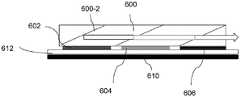
图5展示制造彩色装置的另一种方法。此处,使用二向色棱镜500以组合来自三个单色装置502、504、506的光。单色装置可具有用于形成光的前板502-L、504-L及506-L及用于控制每像素的光输出的背板502-B、504-B及506-G。此外,机械结构502M、504M及506M用于封装、热管理或电连接。此方法的挑战是其非常庞大且不太适合可穿戴电子装置(例如增强现实装置)。其它挑战是装置需要非常精确地对准,此对高像素密度装置来说是困难的。Figure 5 shows another method of fabricating a color device. Here, a dichroic prism 500 is used to combine the light from the three
图6介绍新实施例,其中使用线性色彩组合器600来组合来自不同源602、604及606的色彩。此处,源(图像阵列)是在光组合器的一个侧上。使用反射器600-2将通过光源中的任一者产生的光重新引导到同一方向。反射器还允许来自先前源的图像通过。此处,图像源可为不同类型的发光装置(例如微型LED及/或OLED)。单个背板612可用于驱动与每一图像源相关联的前板。在此类情况下,驱动及接口可共享。在其它情况下,不同背板可用于至少两个不同前板。此处,前板与背板的组合可固定于机械结构上。此处,对准来自图像源在背板(或机械结构)上的位置精度。因此,可在无大量耗用的情况下实现高对准精度。此外,组合结构在所有三个维度上均非常紧凑。此处,还可在后表面600-8上设置另一图像源。在一种情况下,此处的图像源可为图像传感器,所述图像传感器捕获从另一侧600-10通过的光。此传感器可用于追踪功能性、成像等。其它图像源中的一者可是为此图像传感器形成光。两个侧600-8及600-10可为物理结构或仅仅虚拟表面。6 introduces a new embodiment in which a
在一种情况下,反射器600-2、600-4及600-6可为二向色镜(或棱镜)。此处,镜反射低于截止波长的光,且通过在带宽内的光。如果图像源是传感器或显示器,那么布置可不同。以下是用于显示器应用,但是可使用相同原理来开发传感器的设置。以下设置是用于3个光源,但是类似布置可用于更多图像源。假设是通过图像源602产生的波长在W2L与W2H(W2L<W2H)之间,其中W2L及W2H界定镜的通过带宽,通过图像源604产生的波长在W4L与W4H之间(W4L<W4H),且通过图像源606产生的波长在W6L与W6H之间(W4L<W4H)。镜600-2截止波长大于W2H(我们可使用小于W2H以从图像源截去一些不需要的波长)。镜600-4截止波长在W2L与W4H之间(W4H<W2L)(我们可使用小于W4H以从图像源截去一些不需要的波长)。镜600-6截止波长在W4L与W6H之间(W6H<W4L)(我们可使用小于W4H以从图像源截去一些不需要的波长)。此处,镜600-2反射通过光源602产生的光的部分。镜600-4反射通过光源604产生的光的部分,且通过来自镜600-2的光的部分。镜600-6反射通过光源606产生的光的部分,且通过来自镜600-4的光的部分。如果来自源的光具有波长重叠,那么可基于色点或功耗或其它参数的优化来完成截止波长的选择。In one case, the reflectors 600-2, 600-4, and 600-6 may be dichroic mirrors (or prisms). Here, the mirror reflects light below the cutoff wavelength and passes light within the bandwidth. The arrangement may be different if the image source is a sensor or display. The following is for a display application, but the same principles can be used to develop a sensor setup. The following setup is for 3 light sources, but a similar arrangement can be used for more image sources. Assuming that the wavelengths generated by
反射器可由具有不同光学性质的不同光学层制成,或可由光栅结构制成。The reflectors can be made of different optical layers with different optical properties, or can be made of grating structures.
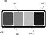
图7展示示范性图像源402、404、406布置的俯视图。前板定位于背板412上。机械结构可用于将结构固持于适当位置中且提供到背板的连接。机械结构可为最终应用的部分(例如增强现实耳机)。7 shows a top view of an
此实施例的一个独特优点是其允许数个图像源的集成,且不限于两个或三个。因此,可集成不同图像源以提供更好功率效率、更用户友好的性能及不同功能。在一种情况下,两种类型的图像源可用于以下图像源中的至少一者:一者具有非常高的色彩纯度,且另一者具有更好的功率或用户友好性能。举例来说,在蓝色的情况下,高强度的纯蓝光会对用户的眼睛造成伤害。因此,可使用两个图像源,一者具有纯蓝色406-1,且另一者具有较浅蓝色406-2。对于需要蓝光的大多数情况,使用浅蓝色图像源406-2。仅当需要纯蓝色时,我们可激活纯蓝色图像源406-1。大体上,浅蓝色具有较高功率效率,此又可提供较低功耗。相同情况还可用于其它图像源。A unique advantage of this embodiment is that it allows the integration of several image sources, not limited to two or three. Therefore, different image sources can be integrated to provide better power efficiency, more user-friendly performance, and different functionality. In one case, two types of image sources can be used for at least one of the following image sources: one with very high color purity and the other with better power or user-friendliness performance. For example, in the case of blue, high-intensity pure blue light can cause damage to the user's eyes. Thus, two image sources can be used, one with a solid blue 406-1 and the other with a lighter blue 406-2. For most situations where blue light is required, a light blue image source 406-2 is used. We can activate pure blue image source 406-1 only when pure blue is required. In general, light blue has higher power efficiency, which in turn provides lower power consumption. The same can be used for other image sources.
在另一实施例中,相同或不同图像源可分别结合小于一个像素偏移使用。因此,当两者同时使用时,其可提供高得多的分辨率图像。In another embodiment, the same or different image sources may each be used with less than one pixel offset. Therefore, when both are used together, it can provide a much higher resolution image.
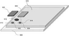
在图9A及9B中演示的另一实施例中,微型装置(阵列)916中的一者形成为连续像素化,其中电流被限制于半导体910的堆叠层的小区域的至少一个区域中以产生隔离微型装置效应(可存在此电流限制结构的阵列来形成微型装置阵列)。在一个实例中,这些堆叠层可为红色外延发光层。堆叠层910经接合到背板900,其中背板中的垫界定子像素。此处,可存在对堆叠层910执行以进一步隔离子像素(阵列)916的后处理。背板900可具有针对像素阵列中的每一像素的多个子像素。可存在针对每一子像素的垫,且电流限制结构(阵列)经接合到背板子像素中的相关联垫。可存在与背板中的垫相关联的多于一个电流限制结构。后处理可包含电流限制、蚀刻堆叠层910中的顶层中的一或多者。在一种情况下,在接合到背板之前,堆叠层可具有通孔912及914。通孔可至少部分填充有导电层,所述导电层用电介质与通孔的壁分离。连接可将来自背板的垫耦合到堆叠层的顶部。在另一种情况下,在堆叠层910经接合到背板中之后,电通孔912及914在堆叠层910中形成。此过程使开口能够与背板中的其它子像素中的垫适当对准。通孔912及914的侧壁可经钝化,且垫902及垫904形成于通孔912及914内部或通孔912及914的壁上。微型装置920及930经接合到垫。可存在针对每一微型装置的多于一个垫或多于两个通孔。导电层可经沉积于微型装置920及930或堆叠层910的顶部上。In another embodiment illustrated in Figures 9A and 9B, one of the microdevices (array) 916 is formed as a continuous pixelation, wherein current is confined in at least one of the small areas of the stacked layers of
在图10A及10B中演示的另一实施例中,微型装置(阵列)1016中的一者形成为连续像素化,其中电流被限制于半导体1010的堆叠层的至少一个区域中以产生隔离微型装置效应(可存在此电流限制结构的阵列来形成微型装置阵列)。在一个实例中,这些堆叠层可为红色外延发光层。堆叠层1010经接合到背板1000,其中背板中的垫界定子像素。此处,可存在对堆叠层1010执行以进一步隔离子像素(阵列)1016的后处理。背板1000可具有针对像素阵列中的每一像素的多个子像素。可存在针对每一子像素的垫1006,且电流限制结构(阵列)经接合到背板子像素中的相关联垫。可存在与背板中的垫1006相关联的多于一个电流限制结构。后处理可包含电流限制、蚀刻堆叠层1010中的顶层中的一或多者。In another embodiment demonstrated in Figures 10A and 10B, one of the microdevices (array) 1016 is formed as a continuous pixelation, wherein current is confined in at least one region of the stacked layers of
在一种情况下,在接合到背板之前,堆叠层可具有通孔1012及1014。通孔允许来自放置于背板上的微型装置的光通过堆叠层1010(或信号到达背板上的微型装置)。在另一种情况下,在堆叠层1010经接合到背板中之后,光学通孔1012及1014在堆叠层1010中形成。此过程使开口能够与背板中的其它子像素中的微型装置1020及1030适当对准。通孔1012及1014的侧壁可经钝化,且在壁上形成反射层。在堆叠层1010的接合之前,微型装置1020及1030经接合到背板。可存在针对每一微型装置的多于一个垫或多于两个通孔。导电层可沉积于微型装置1020及1030或堆叠层1010的顶部上。In one case, the stacked layers may have
凸块1006还可包含类似于1020或1030的微型装置。此处,可形成微型装置以将背板耦合到在装置的顶部上形成的垫。在另一种情况下,测试经接合到背板的微型装置1020及1030的阵列。在分配微型装置以形成凸块1006之前,识别缺陷类型,且为凸块分配的组将包含一些缺陷微型装置。
在另一种情况下,使用例如沉积的其它方法在背板上的经接合微型装置上形成具有电流限制的堆叠层。此处,平坦化层可用于平坦化具有微型装置的背板的表面,且在平坦化层上形成堆叠层。In another case, stack layers with current confinement are formed on the bonded microdevices on the backplane using other methods such as deposition. Here, the planarization layer may be used to planarize the surface of the backplane with the micro-devices, and a stacked layer is formed on the planarization layer.
在图11A、11B及11C中演示的另一实施例中,多于一个微型装置(阵列)1106、1122及1134形成为连续像素化,其中电流被限制于半导体1110、1120及1130的堆叠层的至少一个区域中,以产生隔离微型装置效应(可存在此电流限制结构的阵列来形成微型装置阵列)。在一个实例中,这些堆叠层可为红色、绿色或蓝色外延发光层。堆叠层1110经接合到背板1100,其中背板中的垫界定子像素。此处,可存在对堆叠层1110执行以进一步隔离子像素(阵列)1116的后处理。背板1100可具有针对像素阵列中的每一像素的多个子像素。可存在针对每一子像素的垫,且电流限制结构(阵列)1106经接合到背板子像素中的相关联垫。可存在与背板中的每一相关联垫相关联的多于一个电流限制结构。后处理可包含电流限制、蚀刻堆叠层1110中的顶层中的一或多者。在一种情况下,在接合到背板之前,堆叠层可具有电通孔1112及1114。通孔将相关联垫1102及1104耦合到堆叠层1110(或信号到达背板上的微型装置)。在另一种情况下,在堆叠层1110接合到背板中之后,电通孔1112及1114在堆叠层1110中形成。此过程使开口能够与背板中的其它子像素中的堆叠层1120及1130中的微型装置适当对准。通孔1112及1114的侧壁可经钝化,且可在壁上形成导电层。In another embodiment illustrated in Figures 11A, 11B and 11C, more than one microdevice (array) 1106, 1122 and 1134 is formed as a continuous pixelation in which current is confined to the stacked layers of
堆叠层1120经接合到堆叠层1110的顶部上的背板1100,其中背板中的垫界定子像素。此处,可存在对堆叠层1120执行以进一步隔离子像素(阵列)1122的后处理。背板1100可具有针对像素阵列中的每一像素的多个子像素。可存在针对每一子像素的垫,且电流限制结构(阵列)1122经接合到背板子像素中的相关联垫。可存在与背板中的每一相关联垫相关联的多于一个电流限制结构。后处理可包含电流限制、蚀刻堆叠层1120中的顶层中的一或多者。在一种情况下,在接合到背板之前,堆叠层1120可具有电通孔1124及光学通孔1126。电通孔将相关联垫1104耦合到堆叠层1130。光学通孔允许来自堆叠层1110中的微型装置的光通过堆叠层1120(或信号到达层1110上的微型装置)。在另一种情况下,在堆叠层1120经接合到背板中之后,电通孔1124及光学通孔1126在堆叠层1120中形成。此过程使开口能够与背板中的其它子像素中的堆叠层1110及1130中的微型装置适当对准。通孔1124的侧壁可经钝化,且在壁上形成导电层或从通孔1124内部形成垫。通孔1126的侧壁可经涂布有钝化层及反射层。
堆叠层1130经接合到堆叠层1120的顶部上的背板1100,其中背板中的垫界定子像素。此处,可存在对堆叠层1130执行以进一步隔离子像素(阵列)1134的后处理。背板1100可具有针对像素阵列中的每一像素的多个子像素。可存在针对每一子像素的垫,且电流限制结构(阵列)1134经接合到背板子像素中的相关联垫。可存在与背板中的每一相关联垫相关联的多于一个电流限制结构。后处理可包含电流限制、蚀刻堆叠层1130中的顶层中的一或多者。在一种情况下,在接合到背板之前,堆叠层1130可具有光学通孔1132及1136。光学通孔允许来自堆叠层1110及1120中的微型装置的光通过堆叠层1130(或信号到达层1110及1120上的微型装置)。在另一种情况下,在堆叠层1130经接合到背板1100中之后,光学通孔1136及1132在堆叠层1130中形成。此过程使开口能够与背板中的其它子像素中的堆叠层1110及1120的微型装置适当对准。1132及1136的侧壁可涂布有钝化层及反射层。
在堆叠层1010的接合之前,微型装置1020及1030经接合到背板。可存在针对每一微型装置的多于一个垫或多于两个通孔。导电层可经沉积于微型装置1020及1030或堆叠层1010的顶部上。
虽然已说明及描述本发明的特定实施例及应用,但应了解,本发明不限于本文中所公开的精确构造及组合物,且各种修改、改变及变化可从前述描述显而易见,而不脱离如在所附权利要求书中所界定的本发明的精神及范围。While particular embodiments and applications of the invention have been illustrated and described, it is to be understood that the invention is not limited to the precise constructions and compositions disclosed herein and that various modifications, changes and variations may be apparent from the foregoing description without departing from the The spirit and scope of the present invention is as defined in the appended claims.
Claims (56)
Translated fromChineseApplications Claiming Priority (7)
| Application Number | Priority Date | Filing Date | Title |
|---|---|---|---|
| US201962913795P | 2019-10-11 | 2019-10-11 | |
| US62/913,795 | 2019-10-11 | ||
| US201962924450P | 2019-10-22 | 2019-10-22 | |
| US62/924,450 | 2019-10-22 | ||
| US202063016727P | 2020-04-28 | 2020-04-28 | |
| US63/016,727 | 2020-04-28 | ||
| PCT/CA2020/051363WO2021068082A1 (en) | 2019-10-11 | 2020-10-09 | Color optoelectronic solid state device |
Publications (1)
| Publication Number | Publication Date |
|---|---|
| CN114450809Atrue CN114450809A (en) | 2022-05-06 |
Family
ID=75436979
Family Applications (1)
| Application Number | Title | Priority Date | Filing Date |
|---|---|---|---|
| CN202080068337.XAPendingCN114450809A (en) | 2019-10-11 | 2020-10-09 | Color photoelectric solid-state device |
Country Status (5)
| Country | Link |
|---|---|
| KR (1) | KR20220081350A (en) |
| CN (1) | CN114450809A (en) |
| DE (1) | DE112020004875T5 (en) |
| TW (1) | TW202122846A (en) |
| WO (1) | WO2021068082A1 (en) |
Citations (6)
| Publication number | Priority date | Publication date | Assignee | Title |
|---|---|---|---|---|
| JP2010035134A (en)* | 2008-06-30 | 2010-02-12 | Canon Inc | Mechano-electrical transducer, mechano-electrical transduction device, and method for manufacturing the device |
| WO2011045904A1 (en)* | 2009-10-15 | 2011-04-21 | パナソニック株式会社 | Display panel device, display device, and method for manufacturing display panel device |
| US20180175268A1 (en)* | 2016-12-20 | 2018-06-21 | Lg Display Co., Ltd. | Light emitting diode chip and light emitting diode dsiplay apparatus comprising the same |
| US20180287027A1 (en)* | 2017-03-30 | 2018-10-04 | Vuereal Inc. | Vertical solid-state devices |
| US20180358405A1 (en)* | 2015-01-23 | 2018-12-13 | Vuereal Inc. | Micro device integration into system substrate |
| US20190288156A1 (en)* | 2017-03-30 | 2019-09-19 | Vuereal Inc. | High efficient microdevices |
Family Cites Families (3)
| Publication number | Priority date | Publication date | Assignee | Title |
|---|---|---|---|---|
| TWI614920B (en)* | 2014-05-19 | 2018-02-11 | 晶元光電股份有限公司 | Photoelectric element and method of manufacturing same |
| US10707277B2 (en)* | 2016-10-04 | 2020-07-07 | Vuereal Inc. | Method of integrating functional tuning materials with micro devices and structures thereof |
| KR20190033979A (en)* | 2017-09-22 | 2019-04-01 | 주식회사 루멘스 | vertical type light emitting elements having color conversion electrode part |
- 2020
- 2020-10-09KRKR1020227013796Apatent/KR20220081350A/enactivePending
- 2020-10-09WOPCT/CA2020/051363patent/WO2021068082A1/ennot_activeCeased
- 2020-10-09CNCN202080068337.XApatent/CN114450809A/enactivePending
- 2020-10-09DEDE112020004875.6Tpatent/DE112020004875T5/enactivePending
- 2020-10-12TWTW109135241Apatent/TW202122846A/enunknown
Patent Citations (7)
| Publication number | Priority date | Publication date | Assignee | Title |
|---|---|---|---|---|
| JP2010035134A (en)* | 2008-06-30 | 2010-02-12 | Canon Inc | Mechano-electrical transducer, mechano-electrical transduction device, and method for manufacturing the device |
| WO2011045904A1 (en)* | 2009-10-15 | 2011-04-21 | パナソニック株式会社 | Display panel device, display device, and method for manufacturing display panel device |
| US20180358405A1 (en)* | 2015-01-23 | 2018-12-13 | Vuereal Inc. | Micro device integration into system substrate |
| US20180175268A1 (en)* | 2016-12-20 | 2018-06-21 | Lg Display Co., Ltd. | Light emitting diode chip and light emitting diode dsiplay apparatus comprising the same |
| CN108206234A (en)* | 2016-12-20 | 2018-06-26 | 乐金显示有限公司 | Light-emitting diode chip for backlight unit and the emitting diode display device including the chip |
| US20180287027A1 (en)* | 2017-03-30 | 2018-10-04 | Vuereal Inc. | Vertical solid-state devices |
| US20190288156A1 (en)* | 2017-03-30 | 2019-09-19 | Vuereal Inc. | High efficient microdevices |
Also Published As
| Publication number | Publication date |
|---|---|
| DE112020004875T5 (en) | 2022-06-30 |
| WO2021068082A1 (en) | 2021-04-15 |
| KR20220081350A (en) | 2022-06-15 |
| TW202122846A (en) | 2021-06-16 |
Similar Documents
| Publication | Publication Date | Title |
|---|---|---|
| JP7676404B2 (en) | Bonded Optical Devices | |
| JP7248828B2 (en) | Color ILED display on silicon | |
| TWI747958B (en) | Micro display panels with integrated micro-reflectors | |
| CN112106354B (en) | Architecture for light emitting elements in light field displays | |
| CN119604107A (en) | Systems and methods for multi-color LED pixel units | |
| US20100103389A1 (en) | Multi-MEMS Single Package MEMS Device | |
| CN111615749A (en) | Display panel based on miniature LED | |
| TW201838203A (en) | Fabricating semiconductor components by stacking layers of miniature light-emitting diodes | |
| US8044431B2 (en) | Microdisplay packaging system | |
| CN112106129A (en) | Architecture for light emitting elements in light field displays | |
| JP2024542355A (en) | Hybrid CMOS Micro LED Display Layout | |
| CN115939278A (en) | Semiconductor light emitting device, display apparatus including the same, and method of manufacturing the same | |
| TW202305480A (en) | Color optoelectronic solid state device | |
| CN114450809A (en) | Color photoelectric solid-state device | |
| US20220415861A1 (en) | Color optoelectronic solid state device | |
| CN117480433A (en) | Color optoelectronic solid state device | |
| US12317646B2 (en) | Light-emitting device and display apparatus including the same | |
| JP2005342803A (en) | Mems element, its manufacturing method, optical mems element, optical modulator, glv device and laser display | |
| CN118974954A (en) | Light emitting device and image display device |
Legal Events
| Date | Code | Title | Description |
|---|---|---|---|
| PB01 | Publication | ||
| PB01 | Publication | ||
| SE01 | Entry into force of request for substantive examination | ||
| SE01 | Entry into force of request for substantive examination |