CN114446793A - Manufacturing method of high-voltage MOS device - Google Patents
Manufacturing method of high-voltage MOS deviceDownload PDFInfo
- Publication number
- CN114446793A CN114446793ACN202210376511.8ACN202210376511ACN114446793ACN 114446793 ACN114446793 ACN 114446793ACN 202210376511 ACN202210376511 ACN 202210376511ACN 114446793 ACN114446793 ACN 114446793A
- Authority
- CN
- China
- Prior art keywords
- layer
- active region
- hard mask
- oxide layer
- semiconductor substrate
- Prior art date
- Legal status (The legal status is an assumption and is not a legal conclusion. Google has not performed a legal analysis and makes no representation as to the accuracy of the status listed.)
- Granted
Links
- 238000004519manufacturing processMethods0.000titleclaimsabstractdescription19
- 238000000034methodMethods0.000claimsabstractdescription99
- 230000008569processEffects0.000claimsabstractdescription73
- 239000000758substrateSubstances0.000claimsabstractdescription68
- 239000004065semiconductorSubstances0.000claimsabstractdescription66
- 238000005468ion implantationMethods0.000claimsabstractdescription63
- 238000002513implantationMethods0.000claimsabstractdescription36
- 239000002019doping agentSubstances0.000claimsabstractdescription31
- 239000007943implantSubstances0.000claimsabstractdescription10
- 239000000463materialSubstances0.000claimsdescription55
- 238000002955isolationMethods0.000claimsdescription44
- 229920002120photoresistant polymerPolymers0.000claimsdescription13
- 238000011049fillingMethods0.000claimsdescription8
- VYPSYNLAJGMNEJ-UHFFFAOYSA-NSilicium dioxideChemical compoundO=[Si]=OVYPSYNLAJGMNEJ-UHFFFAOYSA-N0.000claimsdescription7
- 229910052814silicon oxideInorganic materials0.000claimsdescription7
- 229910052581Si3N4Inorganic materials0.000claimsdescription4
- HQVNEWCFYHHQES-UHFFFAOYSA-Nsilicon nitrideChemical compoundN12[Si]34N5[Si]62N3[Si]51N64HQVNEWCFYHHQES-UHFFFAOYSA-N0.000claimsdescription4
- 238000005530etchingMethods0.000claimsdescription2
- 238000002360preparation methodMethods0.000claims1
- 239000010410layerSubstances0.000description166
- 229910052751metalInorganic materials0.000description5
- 239000002184metalSubstances0.000description5
- 238000010586diagramMethods0.000description4
- 239000000126substanceSubstances0.000description4
- XUIMIQQOPSSXEZ-UHFFFAOYSA-NSiliconChemical compound[Si]XUIMIQQOPSSXEZ-UHFFFAOYSA-N0.000description3
- 238000002347injectionMethods0.000description3
- 239000007924injectionSubstances0.000description3
- 230000004048modificationEffects0.000description3
- 238000012986modificationMethods0.000description3
- 229910021420polycrystalline siliconInorganic materials0.000description3
- 229910052710siliconInorganic materials0.000description3
- 239000010703siliconSubstances0.000description3
- 239000000243solutionSubstances0.000description3
- 238000000231atomic layer depositionMethods0.000description2
- QVGXLLKOCUKJST-UHFFFAOYSA-Natomic oxygenChemical compound[O]QVGXLLKOCUKJST-UHFFFAOYSA-N0.000description2
- 230000000903blocking effectEffects0.000description2
- 238000005229chemical vapour depositionMethods0.000description2
- 230000000694effectsEffects0.000description2
- 229910052760oxygenInorganic materials0.000description2
- 239000001301oxygenSubstances0.000description2
- 229920005591polysiliconPolymers0.000description2
- ZOXJGFHDIHLPTG-UHFFFAOYSA-NBoronChemical compound[B]ZOXJGFHDIHLPTG-UHFFFAOYSA-N0.000description1
- GYHNNYVSQQEPJS-UHFFFAOYSA-NGalliumChemical compound[Ga]GYHNNYVSQQEPJS-UHFFFAOYSA-N0.000description1
- OAICVXFJPJFONN-UHFFFAOYSA-NPhosphorusChemical compound[P]OAICVXFJPJFONN-UHFFFAOYSA-N0.000description1
- 229910052785arsenicInorganic materials0.000description1
- RQNWIZPPADIBDY-UHFFFAOYSA-Narsenic atomChemical compound[As]RQNWIZPPADIBDY-UHFFFAOYSA-N0.000description1
- 230000004888barrier functionEffects0.000description1
- 230000015572biosynthetic processEffects0.000description1
- 229910052796boronInorganic materials0.000description1
- 239000011248coating agentSubstances0.000description1
- 238000000576coating methodMethods0.000description1
- 239000013078crystalSubstances0.000description1
- 230000007547defectEffects0.000description1
- 238000001312dry etchingMethods0.000description1
- 239000010408filmSubstances0.000description1
- 229910052733galliumInorganic materials0.000description1
- 238000000227grindingMethods0.000description1
- 239000012535impuritySubstances0.000description1
- 229910021421monocrystalline siliconInorganic materials0.000description1
- 229910052698phosphorusInorganic materials0.000description1
- 239000011574phosphorusSubstances0.000description1
- 238000005498polishingMethods0.000description1
- 230000008439repair processEffects0.000description1
- 239000002356single layerSubstances0.000description1
- 238000000427thin-film depositionMethods0.000description1
Images


Classifications
- H—ELECTRICITY
- H10—SEMICONDUCTOR DEVICES; ELECTRIC SOLID-STATE DEVICES NOT OTHERWISE PROVIDED FOR
- H10D—INORGANIC ELECTRIC SEMICONDUCTOR DEVICES
- H10D30/00—Field-effect transistors [FET]
- H10D30/01—Manufacture or treatment
- H10D30/021—Manufacture or treatment of FETs having insulated gates [IGFET]
- H10D30/027—Manufacture or treatment of FETs having insulated gates [IGFET] of lateral single-gate IGFETs
- H—ELECTRICITY
- H01—ELECTRIC ELEMENTS
- H01L—SEMICONDUCTOR DEVICES NOT COVERED BY CLASS H10
- H01L21/00—Processes or apparatus adapted for the manufacture or treatment of semiconductor or solid state devices or of parts thereof
- H01L21/02—Manufacture or treatment of semiconductor devices or of parts thereof
- H01L21/04—Manufacture or treatment of semiconductor devices or of parts thereof the devices having potential barriers, e.g. a PN junction, depletion layer or carrier concentration layer
- H01L21/18—Manufacture or treatment of semiconductor devices or of parts thereof the devices having potential barriers, e.g. a PN junction, depletion layer or carrier concentration layer the devices having semiconductor bodies comprising elements of Group IV of the Periodic Table or AIIIBV compounds with or without impurities, e.g. doping materials
- H01L21/26—Bombardment with radiation
- H01L21/263—Bombardment with radiation with high-energy radiation
- H01L21/265—Bombardment with radiation with high-energy radiation producing ion implantation
- H01L21/26586—Bombardment with radiation with high-energy radiation producing ion implantation characterised by the angle between the ion beam and the crystal planes or the main crystal surface
- H—ELECTRICITY
- H10—SEMICONDUCTOR DEVICES; ELECTRIC SOLID-STATE DEVICES NOT OTHERWISE PROVIDED FOR
- H10D—INORGANIC ELECTRIC SEMICONDUCTOR DEVICES
- H10D62/00—Semiconductor bodies, or regions thereof, of devices having potential barriers
- H10D62/10—Shapes, relative sizes or dispositions of the regions of the semiconductor bodies; Shapes of the semiconductor bodies
Landscapes
- Physics & Mathematics (AREA)
- High Energy & Nuclear Physics (AREA)
- Engineering & Computer Science (AREA)
- General Physics & Mathematics (AREA)
- Health & Medical Sciences (AREA)
- Toxicology (AREA)
- Crystallography & Structural Chemistry (AREA)
- Condensed Matter Physics & Semiconductors (AREA)
- Chemical & Material Sciences (AREA)
- Manufacturing & Machinery (AREA)
- Computer Hardware Design (AREA)
- Microelectronics & Electronic Packaging (AREA)
- Power Engineering (AREA)
- Element Separation (AREA)
- Insulated Gate Type Field-Effect Transistor (AREA)
- Metal-Oxide And Bipolar Metal-Oxide Semiconductor Integrated Circuits (AREA)
Abstract
Translated fromChinese
Description
Translated fromChinese技术领域technical field
本发明涉及半导体制造技术领域,特别涉及一种高压MOS器件的制作方法。The invention relates to the technical field of semiconductor manufacturing, in particular to a manufacturing method of a high-voltage MOS device.
背景技术Background technique
近年来高压MOS器件(HV MOS)的应用日益广泛,例如电源控制和驱动电路等领域,其工作电压在几十伏甚至上百伏。In recent years, high-voltage MOS devices (HV MOS) have been widely used, such as power supply control and driving circuits, and their operating voltages are tens of volts or even hundreds of volts.
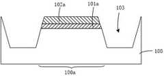
图1为一种高压MOS器件的结构示意图。如图1所示,用于形成高压MOS器件的半导体基底100包括有源区100a(AA),有源区100a通过隔离结构104限定。高压MOS器件的栅氧化层101a形成在有源区100a的半导体基底上,如图1所示,栅氧化层101a的截面(沿有源区100a的Width方向上的截面)例如为双喇叭口的形状,即栅氧化层101a具有位于有源区100a边缘区域上的凸峰(Hump),使得栅氧化层101a边缘区域的厚度大于其中间区域的厚度。后续在对有源区100a进行离子注入形成高压注入阱106时,由于栅氧化层101a不同区域的厚度差别,导致有源区100a边缘区域的注入剂量(IMP dose)少于中间区域的注入剂量,从而形成的高压注入阱106的边缘区域(图1中的虚线框内)的掺杂浓度小于中间区域的掺杂浓度,如此在对栅极107施加电压时,会导致高压注入阱106边角(corner)的漏电(Leak)增加,或者导致高压MOS器件提前开启,进而降低了高压MOS器件的阈值电压稳定性(Vthstability,VTS)。FIG. 1 is a schematic structural diagram of a high-voltage MOS device. As shown in FIG. 1 , a
发明内容SUMMARY OF THE INVENTION
本发明的目的之一是提供一种高压MOS器件的制作方法,可以提高高压注入阱掺杂浓度的均匀性,降低高压注入阱边角的漏电以及提高高压MOS器件的阈值电压稳定性。One of the objectives of the present invention is to provide a method for manufacturing a high-voltage MOS device, which can improve the uniformity of the doping concentration of the high-voltage injection well, reduce the leakage at the corners of the high-voltage injection well, and improve the threshold voltage stability of the high-voltage MOS device.
为了实现上述目的,本发明提供一种高压MOS器件的制作方法。所述高压MOS器件的制作方法包括:In order to achieve the above object, the present invention provides a method for fabricating a high-voltage MOS device. The manufacturing method of the high-voltage MOS device includes:
提供半导体基底,所述半导体基底包括隔离结构和由所述隔离结构限定的有源区,所述半导体基底上形成有栅氧化层和硬掩模层,所述栅氧化层和所述硬掩模层依次覆盖所述有源区的半导体基底上表面;所述有源区包括靠近所述隔离结构的边缘区域和远离所述隔离结构的中心区域,位于所述有源区的边缘区域上的栅氧化层的厚度大于位于所述有源区的中心区域上的栅氧化层的厚度;A semiconductor substrate is provided, the semiconductor substrate includes an isolation structure and an active region defined by the isolation structure, a gate oxide layer and a hard mask layer are formed on the semiconductor substrate, the gate oxide layer and the hard mask are formed The layers sequentially cover the upper surface of the semiconductor substrate of the active area; the active area includes an edge area close to the isolation structure and a center area away from the isolation structure, and a gate located on the edge area of the active area The thickness of the oxide layer is greater than the thickness of the gate oxide layer on the central region of the active region;
以所述硬掩模层为掩膜,执行第一离子注入工艺,倾斜地向所述有源区的边缘区域注入掺杂物质;以及Using the hard mask layer as a mask, a first ion implantation process is performed, and dopant is implanted obliquely into the edge region of the active region; and
去除所述硬掩模层,执行第二离子注入工艺,向所述有源区注入掺杂物质,在所述有源区的半导体基底顶部形成高压注入阱,其中,所述第一离子注入工艺和所述第二离子注入工艺注入的掺杂物质的导电类型相同。removing the hard mask layer, performing a second ion implantation process, implanting dopants into the active region, and forming a high voltage implantation well on top of the semiconductor substrate in the active region, wherein the first ion implantation process The conductivity type of the dopant implanted in the second ion implantation process is the same.
可选的,位于所述有源区的边缘区域上的栅氧化层的最大厚度比位于所述有源区的中心区域上的栅氧化层的平均厚度大10nm以上。Optionally, the maximum thickness of the gate oxide layer on the edge region of the active region is greater than the average thickness of the gate oxide layer on the central region of the active region by more than 10 nm.
可选的,所述第一离子注入工艺的注入角度为10°~30°。Optionally, the implantation angle of the first ion implantation process is 10°˜30°.
可选的,根据所述硬掩膜层下表面与所述隔离结构上表面之间的高度差选择所述第一离子注入工艺的注入能量。Optionally, the implantation energy of the first ion implantation process is selected according to the height difference between the lower surface of the hard mask layer and the upper surface of the isolation structure.
可选的,所述第一离子注入工艺和所述第二离子注入工艺注入的掺杂物质相同。Optionally, the dopants implanted in the first ion implantation process and the second ion implantation process are the same.
可选的,所述提供半导体基底,所述半导体基底包括隔离结构和由所述隔离结构限定的有源区,所述半导体基底上形成有栅氧化层和硬掩模层的方法包括:Optionally, the method for providing a semiconductor substrate, the semiconductor substrate including an isolation structure and an active region defined by the isolation structure, and forming a gate oxide layer and a hard mask layer on the semiconductor substrate includes:
提供半导体基底;provide semiconductor substrates;
依次形成氧化材料层和硬掩膜材料层,所述氧化材料层和所述硬掩模材料层覆盖所述半导体基底的上表面;forming an oxide material layer and a hard mask material layer in sequence, the oxide material layer and the hard mask material layer covering the upper surface of the semiconductor substrate;
形成图形化的光刻胶层,以所述图形化的光刻胶层为掩膜,刻蚀所述硬掩膜材料层并露出所述氧化材料层的上表面,剩余的所述硬掩膜材料层作为所述硬掩模层;forming a patterned photoresist layer, using the patterned photoresist layer as a mask, etching the hard mask material layer and exposing the upper surface of the oxide material layer, and the remaining hard mask a material layer as the hard mask layer;
以所述硬掩模层为掩膜,向下刻蚀所述氧化材料层和所述半导体基底,并停止在所述半导体基底中,形成沟槽,剩余的所述氧化材料层作为所述栅氧化层;Using the hard mask layer as a mask, etch the oxide material layer and the semiconductor substrate downward, and stop in the semiconductor substrate to form a trench, and the remaining oxide material layer is used as the gate oxide layer;
形成线形氧化层,所述线形氧化层保形地覆盖在所述沟槽的内表面;forming a linear oxide layer conformally covering the inner surface of the trench;
在所述沟槽内填满隔离介质层,形成所述隔离结构;Filling the trench with an isolation dielectric layer to form the isolation structure;
其中,在形成所述线形氧化层的过程中,位于所述有源区的边缘区域上的栅氧化层的厚度增加。Wherein, in the process of forming the linear oxide layer, the thickness of the gate oxide layer located on the edge region of the active region increases.
可选的,采用高温炉管工艺形成所述线形氧化层。Optionally, the linear oxide layer is formed by using a high temperature furnace tube process.
可选的,所述栅氧化层和所述线形氧化层的材料均包括氧化硅。Optionally, materials of the gate oxide layer and the linear oxide layer both include silicon oxide.
可选的,所述硬掩模层的材料层包括氮化硅。Optionally, the material layer of the hard mask layer includes silicon nitride.
可选的,在所述有源区的半导体基底顶部形成所述高压注入阱后,所述高压MOS器件的制作方法包括:Optionally, after the high-voltage implantation well is formed on the top of the semiconductor substrate of the active region, the manufacturing method of the high-voltage MOS device includes:
在所述有源区上形成栅极,且所述栅极从所述有源区上方延伸至与所述有源区相邻的隔离结构的上方。A gate is formed on the active region, and the gate extends from above the active region to over an isolation structure adjacent to the active region.
本发明的高压MOS器件的制作方法中,首先,提供包括有源区的半导体基底,半导体基底上形成有栅氧化层和硬掩模层,所述栅氧化层和所述硬掩模层依次覆盖所述有源区的半导体基底上表面,且位于有源区的边缘区域上的栅氧化层的厚度大于位于有源区的中心区域上的栅氧化层的厚度,即栅氧化层边缘区域的厚度大于其中心区域的厚度;然后,以所述硬掩模层为掩膜,执行第一离子注入工艺,倾斜地向所述有源区的边缘区域注入掺杂物质;接着,去除所述硬掩模层,执行第二离子注入工艺,向有源区注入掺杂物质,在有源区的半导体基底顶部形成高压注入阱,第一离子注入工艺和第二离子注入工艺注入的掺杂物质的导电类型相同。由于栅氧化层边缘区域的厚度较中心区域的厚度厚,边缘区域的栅氧化层对掺杂物质的阻挡能力大于中心区域的栅氧化层,因而仅通过第二离子注入工艺形成高压注入阱时,会导致有源区中心区域的注入剂量大于边缘区域的注入剂量,本发明的高压MOS器件的制作方法中,通过第一离子注入工艺来补偿第二离子注入工艺中有源区的边缘区域的注入剂量较少的问题,从而可以提高形成的高压注入阱的掺杂浓度的均匀性,降低高压注入阱边角的漏电以及提高高压MOS器件的阈值电压稳定性,提高高压MOS器件的电性能;而且,在执行第一离子注入工艺时,以现有的硬掩模层为掩膜,如此可以在不增加掩膜成本的情况下提高高压注入阱的掺杂浓度均匀性,有助于节约生产成本。In the manufacturing method of the high-voltage MOS device of the present invention, first, a semiconductor substrate including an active region is provided, a gate oxide layer and a hard mask layer are formed on the semiconductor substrate, and the gate oxide layer and the hard mask layer are sequentially covered The upper surface of the semiconductor substrate of the active region, and the thickness of the gate oxide layer located on the edge region of the active region is greater than the thickness of the gate oxide layer located on the central region of the active region, that is, the thickness of the edge region of the gate oxide layer greater than the thickness of its central region; then, using the hard mask layer as a mask, a first ion implantation process is performed, and dopant is implanted obliquely to the edge region of the active region; then, the hard mask is removed A mold layer, performing a second ion implantation process, implanting dopant substances into the active area, forming a high-voltage implantation well on the top of the semiconductor substrate in the active area, and conducting conductivity of the dopant substances implanted in the first ion implantation process and the second ion implantation process same type. Since the thickness of the edge region of the gate oxide layer is thicker than that of the center region, the gate oxide layer in the edge region has a greater blocking ability to dopants than the gate oxide layer in the center region. Therefore, when the high-voltage implantation well is formed only by the second ion implantation process, The implant dose in the central region of the active region is larger than the implant dose in the edge region. In the manufacturing method of the high-voltage MOS device of the present invention, the first ion implantation process is used to compensate the implantation in the edge region of the active region in the second ion implantation process. The problem of less dose can improve the uniformity of the doping concentration of the formed high-voltage implanted well, reduce the leakage at the corners of the high-voltage implanted well, improve the threshold voltage stability of the high-voltage MOS device, and improve the electrical performance of the high-voltage MOS device; and , when performing the first ion implantation process, the existing hard mask layer is used as a mask, so that the uniformity of the doping concentration of the high-voltage implanted well can be improved without increasing the cost of the mask, which is helpful for saving production costs .
附图说明Description of drawings
图1为一种高压MOS器件的结构示意图。FIG. 1 is a schematic structural diagram of a high-voltage MOS device.
图2为本发明一实施例的高压MOS器件的制作方法的流程图。FIG. 2 is a flowchart of a method for fabricating a high-voltage MOS device according to an embodiment of the present invention.
图3至图10为本发明一实施例的高压MOS器件的制作方法的分步骤结构示意图。3 to 10 are schematic structural diagrams of steps of a method for fabricating a high-voltage MOS device according to an embodiment of the present invention.
附图标记说明:100-半导体基底;101-氧化材料层;101a-栅氧化层;102-硬掩模材料层;102a-硬掩膜层;103-沟槽;104a-线形氧化层;104b-隔离介质层;104-隔离结构;105-掺杂区;106-高压注入阱;107-栅极;108-侧墙;109-接触插塞;110-金属导线。Description of reference numerals: 100-semiconductor substrate; 101-oxide material layer; 101a-gate oxide layer; 102-hard mask material layer; 102a-hard mask layer; 103-trench; 104a-linear oxide layer; 104-isolation structure; 105-doped region; 106-high voltage injection well; 107-gate; 108-spacer; 109-contact plug; 110-metal wire.
具体实施方式Detailed ways
以下结合附图和具体实施例对本发明提出的高压MOS器件的制作方法作进一步详细说明。根据下面的说明,本发明的优点和特征将更清楚。需说明的是,附图均采用非常简化的形式且均使用非精准的比例,仅用以方便、明晰地辅助说明本发明实施例的目的。The manufacturing method of the high-voltage MOS device proposed by the present invention will be further described in detail below with reference to the accompanying drawings and specific embodiments. The advantages and features of the present invention will become more apparent from the following description. It should be noted that, the accompanying drawings are all in a very simplified form and in inaccurate scales, and are only used to facilitate and clearly assist the purpose of explaining the embodiments of the present invention.
为了提高高压注入阱掺杂浓度的均匀性,降低高压注入阱边角的漏电以及提高高压MOS器件的阈值电压稳定性,本实施例提供一种高压MOS器件的制作方法。图2为本发明一实施例的高压MOS器件的制作方法的流程图,如图2所示,所述高压MOS器件的制作方法包括:In order to improve the uniformity of the doping concentration of the high-voltage implanted well, reduce the leakage at the corners of the high-voltage implanted well, and improve the threshold voltage stability of the high-voltage MOS device, this embodiment provides a manufacturing method of a high-voltage MOS device. FIG. 2 is a flowchart of a method for fabricating a high-voltage MOS device according to an embodiment of the present invention. As shown in FIG. 2 , the fabricating method for the high-voltage MOS device includes:
S1,提供半导体基底,所述半导体基底包括隔离结构和由所述隔离结构限定的有源区,所述半导体基底上形成有栅氧化层和硬掩模层,所述栅氧化层和所述硬掩模层依次覆盖所述有源区的半导体基底上表面;所述有源区包括靠近所述隔离结构的边缘区域和远离所述隔离结构的中心区域,位于所述有源区的边缘区域上的栅氧化层的厚度大于位于所述有源区的中心区域上的栅氧化层的厚度;S1, a semiconductor substrate is provided, the semiconductor substrate includes an isolation structure and an active region defined by the isolation structure, a gate oxide layer and a hard mask layer are formed on the semiconductor substrate, the gate oxide layer and the hard mask layer are formed on the semiconductor substrate The mask layer sequentially covers the upper surface of the semiconductor substrate of the active area; the active area includes an edge area close to the isolation structure and a center area away from the isolation structure, located on the edge area of the active area The thickness of the gate oxide layer is greater than the thickness of the gate oxide layer located on the central region of the active region;
S2,以所述硬掩模层为掩膜,执行第一离子注入工艺,倾斜地向所述有源区的边缘区域注入掺杂物质;S2, using the hard mask layer as a mask, performing a first ion implantation process, and implanting a dopant into the edge region of the active region obliquely;
S3,去除所述硬掩模层,执行第二离子注入工艺,向所述有源区注入掺杂物质,在所述有源区的半导体基底顶部形成高压注入阱,其中,所述第一离子注入工艺和所述第二离子注入工艺注入的掺杂物质的导电类型相同。S3, removing the hard mask layer, performing a second ion implantation process, implanting dopants into the active region, and forming a high-voltage implantation well on top of the semiconductor substrate in the active region, wherein the first ion implantation The conductivity type of the dopant implanted by the implantation process and the second ion implantation process is the same.
图3至图10为本发明一实施例的高压MOS器件的制作方法的分步骤结构示意图。以下结合图2以及图3至图10对本实施例的高压MOS器件的制作方法进行说明。3 to 10 are schematic structural diagrams of steps of a method for fabricating a high-voltage MOS device according to an embodiment of the present invention. The fabrication method of the high-voltage MOS device of this embodiment will be described below with reference to FIG. 2 and FIGS. 3 to 10 .
步骤S1中,提供半导体基底,所述半导体基底包括隔离结构和由所述隔离结构限定的有源区,所述半导体基底上形成有栅氧化层和硬掩模层的方法可以包括分步骤S11至S16。In step S1, a semiconductor substrate is provided, the semiconductor substrate includes an isolation structure and an active region defined by the isolation structure, and the method for forming a gate oxide layer and a hard mask layer on the semiconductor substrate may include steps S11 to S16.
分步骤S11,如图3所示,提供半导体基底100。所述半导体基底100的材料包括但不限于单晶或多晶半导体材料,另外,还可以是本征单晶硅衬底或者是轻微掺杂的硅衬底,进一步地,可以为N型多晶硅衬底或P型多晶硅衬底。In step S11, as shown in FIG. 3, a
分步骤S12,如图3所示,依次形成氧化材料层101和硬掩膜材料层102,所述氧化材料层101和所述硬掩模材料层102覆盖所述半导体基底100的上表面。所述氧化材料层101和所述硬掩模材料层102可以采用化学气相沉积工艺(CVD)或原子层沉积工艺(ALD)等本领域公知的薄膜沉积工艺形成,在此不做限定。所述氧化材料层101的材料可以包括氧化硅。所述硬掩模材料层102的材料可以包括氮化硅或氮氧化硅等。所述硬掩模材料层102可以为单层结构或由不同材料层构成的多层结构。In step S12 , as shown in FIG. 3 , an
分步骤S13,参考图3和图4,形成图形化的光刻胶层(图中未示出),以所述图形化的光刻胶层为掩膜,刻蚀所述硬掩膜材料层102并露出所述氧化材料层101的上表面,剩余的所述硬掩膜材料层作为所述硬掩模层102a。形成图形化的光刻胶层的方法可以包括:在硬掩模材料层102上涂布光刻胶形成光刻胶层,对光刻胶层进行曝光和显影,形成图形化的光刻胶层,再对图形化的光刻胶层进行后烘烤,以进一步固化所述图形化的光刻胶层。In step S13, referring to FIG. 3 and FIG. 4, a patterned photoresist layer (not shown in the figure) is formed, and the hard mask material layer is etched using the patterned photoresist layer as a
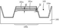
分步骤S14,参考图4,以所述硬掩模层102a为掩膜,向下刻蚀所述氧化材料层101和所述半导体基底100,并停止在所述半导体基底100中,形成沟槽103,剩余的所述氧化材料层作为所述栅氧化层101a。本实施例中,可以采用干法刻蚀工艺刻蚀所述氧化材料层101和所述半导体基底100形成所述沟槽103,形成的沟槽103的数量可以为多个。图4中,所述沟槽103的截面形状为倒梯形。但不限于此,在其它实施例中,所述沟槽103的截面形状可以为矩形等其它形状。所述硬掩模层102a的材料可以包括氮化硅。Step S14, referring to FIG. 4, using the
分步骤S15,如图5所示,形成线形氧化层104a,所述线形氧化层104a可以保形地覆盖在所述沟槽103的内表面。本实施例中,所述栅氧化层101a和所述线形氧化层104a的材料均可以包括氧化硅。所述线形氧化层104a可以采用高温炉管工艺形成。所述线形氧化层104a可以修复沟槽103表面的缺陷,提高隔离结构的隔离效果。In step S15 , as shown in FIG. 5 , a
本实施例中,在形成线形氧化层104a的过程中,位于有源区100a的边缘区域上的栅氧化层101a的厚度增加,使得位于有源区100a的边缘区域上的栅氧化层的厚度大于位于有源区100a的中心区域上的栅氧化层的厚度,即使得栅氧化层101a边缘区域的厚度大于其中心区域的厚度。In this embodiment, in the process of forming the
具体的,在形成线形氧化层104a的过程中,氧气从沟槽103的侧表面扩散进入到有源区100a的边缘区域并与半导体基底100中的硅反应形成氧化硅,从而在有源区100a的边缘区域,栅氧化层101a的厚度会增厚;而由于硬掩模层102a的覆盖阻挡,氧气难以扩散到有源区100a的中心区域,从而栅氧化层101a中心区域的厚度不会增厚。而且,在形成线形氧化层104a的过程中,半导体基底100处在温度较高的环境中,栅氧化层101a的边缘会被圆化,如此也会使得栅氧化层101a边缘区域的厚度大于中心区域的厚度。Specifically, in the process of forming the
如图5所示,从中心到边缘的方向上,栅氧化层101a的边缘区域的厚度逐渐增大;或者说,对于边缘区域的栅氧化层,其与中心区域相接的位置厚度最小,与隔离结构104相接的位置厚度最大;或者说,栅氧化层101a的截面为双喇叭口的形状;或者说,栅氧化层101a具有位于有源区100a边缘区域上的凸峰,且凸峰朝向半导体基底100的方向凸起。As shown in FIG. 5 , from the center to the edge, the thickness of the edge region of the
本实施例中,参考图5,位于所述有源区100a的边缘区域上的栅氧化层的最大厚度H2比位于所述有源区100a的中心区域上的栅氧化层的平均厚度H1大10nm以上。但不限于此,H2与H1的厚度之差可以视具体工艺条件而定。In this embodiment, referring to FIG. 5 , the maximum thickness H2 of the gate oxide layer on the edge region of the
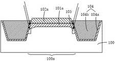
分步骤S16,参考图6,在所述沟槽103内填满隔离介质层104b,形成所述隔离结构104。分步骤S16具体可以包括:在半导体基底100上形成填充材料层,所述填充材料层填满所述沟槽103且覆盖所述硬掩模层102a的上表面;利用化学机械研磨工艺(CMP)对填充材料层进行平坦化处理,去除所述硬掩模层102a上方的填充材料层,剩余的填充材料层作为所述隔离介质层104b。需要说明的是,如图6所示,由于隔离介质层104b和硬掩模层102a的研磨选择比不同,在CMP之后,所述隔离介质层104b的上表面会以略微低于所述硬掩膜层102a的上表面。本实施例中,所述隔离介质层104b的材料可以包括氧化硅。In step S16 , referring to FIG. 6 , the
需要说明的是,本实施例中,高压MOS器件的栅氧化层101a在形成隔离结构104之前形成,在形成线形氧化层104a的过程中,虽然栅氧化层101a的边缘区域的厚度会略微增厚,但是由于高压MOS器件的栅氧化层总体相对较厚,故而栅氧化层101a的边缘区域的厚度略微增加不会对器件的电性能造成较大影响。但是,栅氧化层101a这样的厚度变化对于栅氧化层的厚度较薄的器件(例如中压MOS器件或低压MOS器件)的电性能的影响是致命的,因此,中压MOS器件和低压MOS器件的栅氧化层通常是在隔离结构形成之后、甚至是形成注入阱之后再形成。It should be noted that, in this embodiment, the
接着,执行步骤S2,如图7所示,以所述硬掩模层102a为掩膜,执行第一离子注入工艺,倾斜地向所述有源区100a的边缘区域注入掺杂物质,使得有源区100a的边缘区域形成具有一定掺杂浓度的掺杂区105。Next, step S2 is performed. As shown in FIG. 7 , using the
在第一离子注入工艺中,当注入角度过大时,掺杂区105容易过多的延伸到硬掩膜层102a下方从而存在掺杂物进入有源区100a的中心区域的风险;而当注入角度过小时,位于有源区100a的边缘区域内的掺杂区105的范围过小,即掺杂区105补偿的范围过小。也就是说,注入角度过大或过小均不利于提高后续形成的高压注入阱的掺杂浓度的均匀性。综合考虑后,本实施例中,所述第一离子注入工艺的注入角度可以设置为10°~30°,其中,注入角度的基准线为半导体基底100上表面的法线。In the first ion implantation process, when the implantation angle is too large, the
本实施例中,可以根据所述硬掩膜层下表面与所述隔离结构上表面之间的高度差选择所述第一离子注入工艺的注入能量。第一离子注入工艺的注入能量的选择可以根据实际情况调整。In this embodiment, the implantation energy of the first ion implantation process may be selected according to the height difference between the lower surface of the hard mask layer and the upper surface of the isolation structure. The selection of the implantation energy of the first ion implantation process can be adjusted according to the actual situation.
执行步骤S3,如图8所示,去除所述硬掩模层102a,如图9所示,执行第二离子注入工艺,向所述有源区100a注入掺杂物质,在所述有源区100a的半导体基底顶部形成高压注入阱106,其中,所述第一离子注入工艺和所述第二离子注入工艺注入的掺杂物质的导电类型相同。Step S3 is performed, as shown in FIG. 8 , the
由于栅氧化层101a边缘区域的厚度较中心区域的厚度厚,边缘区域的栅氧化层对掺杂物质的阻挡能力大于中心区域的栅氧化层,因而在第二离子注入工艺中,有源区100a中心区域的注入剂量会大于边缘区域的注入剂量,本实施例中,第一离子注入工艺在有源区100a的边缘区域注入的掺杂物质可以补偿有源区100a的边缘区域的注入剂量,即通过第一离子注入工艺和第二离子注入工艺的组合,可以解决由于栅氧化层101a厚度不均匀导致的有源区100a的注入剂量不均匀的问题,可以提高形成的高压注入阱106的掺杂浓度的均匀性。Since the thickness of the edge region of the
本实施例中,第二离子注入工艺可以垂直的向有源区100a注入掺杂物质。但不限于此,第二离子注入工艺的注入角度可以根据实际需要调整。需要说明的是,在图9中,形成的高压注入阱106已经覆盖了掺杂区105,故图9中未示出掺杂区。In this embodiment, the second ion implantation process may vertically implant dopant into the
所述第一离子注入工艺和所述第二离子注入工艺注入的掺杂物质可以根据半导体基底100的导电类型以及需要形成的高压注入阱106的导电类型选择。例如,当需要形成P型的高压注入阱时,第一离子注入工艺和第二离子注入工艺注入的掺杂物质可以为硼或/和镓等;当需要形成N型的高压注入阱时,第一离子注入工艺和第二离子注入工艺注入的掺杂物质可以为磷或/和砷等。为了便于确定(计算)第一离子注入工艺的注入剂量,本实施例中,第一离子注入工艺和第二离子注入工艺注入的掺杂物质可以相同。The dopant implanted in the first ion implantation process and the second ion implantation process may be selected according to the conductivity type of the
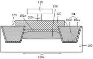
如图10所示,在所述有源区100a的半导体基底顶部形成所述高压注入阱106后,所述高压MOS器件的制作方法可以包括:在所述有源区100a上形成栅极107,栅极107位于栅氧化层101a的上方,且所述栅极107从所述有源区100a上方延伸至与所述有源区100a相邻的隔离结构104的上方,如此可以确保栅极107在有源区100a的宽度方向上(即width方向,图10的水平方向)覆盖有源区100a,确保栅极107的控制能力,提高高压MOS器件的性能。As shown in FIG. 10 , after the high-voltage implantation well 106 is formed on the top of the semiconductor substrate of the
栅极107的材料可以包括多晶硅或金属。当栅极107的材料包括金属时,栅极107可以由多层金属堆叠而成。The material of the
在形成栅极107后,所述高压MOS器件的制作方法还可以包括:形成栅极107的侧墙108,侧墙108覆盖栅极107的侧壁;以栅极107和侧墙108为掩膜,对栅极和侧墙两侧的有源区进行离子注入,形成源极区和漏极区(图中未示出),其中,源极区-栅极-漏极区可以沿有源区100a的长度方向(Length方向)排布,有源区100a的长度方向与其宽度方向相互垂直;在所述栅极107的上方形成接触插塞109以及与接触插塞109连接的金属导线110。After the
本实施例的高压MOS器件的制作方法包括:提供半导体基底100,所述半导体基底100包括隔离结构104和由所述隔离结构104限定的有源区100a,所述半导体基底100上形成有栅氧化层101a和硬掩模层102a,所述栅氧化层101a和所述硬掩模层102b依次覆盖所述有源区100a的半导体基底上表面;所述有源区100a包括靠近所述隔离结构104的边缘区域和远离所述隔离结构104的中心区域,位于所述有源区100a的边缘区域上的栅氧化层的厚度大于位于所述有源区100b的中心区域上的栅氧化层的厚度,即栅氧化层101a边缘区域的厚度大于其中心区域的厚度;以所述硬掩模层102a为掩膜,执行第一离子注入工艺,倾斜地向所述有源区100a的边缘区域注入掺杂物质;以及去除所述硬掩模层102a,执行第二离子注入工艺,向所述有源区100a注入掺杂物质,在所述有源区的半导体基底顶部形成高压注入阱106,其中,所述第一离子注入工艺和所述第二离子注入工艺注入的掺杂物质的导电类型相同。本实施例的高压MOS器件的制作方法中,通过第一离子注入工艺来补偿第二离子注入工艺中有源区100a的边缘区域的注入剂量较少的问题,从而可以提高形成的高压注入阱106的掺杂浓度的均匀性,降低高压注入阱106边角的漏电以及提高高压MOS器件的阈值电压稳定性,提高高压MOS器件的电性能;而且,在执行第一离子注入工艺时,以现有的硬掩模层102a为掩膜,如此可以在不增加掩膜成本的情况下提高了高压注入阱的掺杂浓度均匀性,有助于节约生产成本。The method for fabricating a high-voltage MOS device in this embodiment includes: providing a semiconductor substrate 100, the semiconductor substrate 100 including an isolation structure 104 and an active region 100a defined by the isolation structure 104, and a gate oxide is formed on the semiconductor substrate 100 Layer 101a and hard mask layer 102a, the gate oxide layer 101a and the hard mask layer 102b sequentially cover the upper surface of the semiconductor substrate of the active region 100a; the active region 100a includes the isolation structure 104 close to the The thickness of the gate oxide layer located on the edge region of the active region 100a is greater than the thickness of the gate oxide layer located on the center region of the active region 100b, That is, the thickness of the edge region of the gate oxide layer 101a is greater than the thickness of the central region; using the hard mask layer 102a as a mask, perform the first ion implantation process, and implant dopant into the edge region of the active region 100a obliquely and removing the hard mask layer 102a, performing a second ion implantation process, implanting dopant substances into the active region 100a, and forming a high-voltage implantation well 106 on top of the semiconductor substrate of the active region, wherein the The conductivity type of the dopant implanted in the first ion implantation process and the second ion implantation process is the same. In the method for fabricating a high-voltage MOS device in this embodiment, the first ion implantation process is used to compensate for the problem of less implantation dose in the edge region of the
如在本申请中所使用的术语“第一”、“第二”、“第三”仅用于描述目的,而不能理解为指示或暗示相对重要性或者隐含指明所指示的技术特征的数量。由此,限定有“第一”、“第二”、“第三”的特征可以明示或者隐含地包括一个或者至少两个该特征,除非内容另外明确指出外。The terms "first", "second" and "third" as used in this application are for descriptive purposes only and should not be construed to indicate or imply relative importance or to imply indicate the number of technical features indicated . Thus, features defined as "first", "second", "third" may expressly or implicitly include one or at least both of those features, unless the content clearly dictates otherwise.
贯穿整个说明书中提及的“一实施例”或“本实施例”表示与实施例一起描述的特定部件、结构或特征包括在至少一个实施例中。因此,在贯穿整个说明书中的各个地方出现的短语“一实施例”或“本实施例”不是必须表示同样的实施例。而且,在一个或多个实施例中,特定部件、结构或特征可以以任意合适的方式组合。Reference throughout this specification to "an embodiment" or "the present embodiment" means that a particular component, structure, or feature described in connection with the embodiment is included in at least one embodiment. Thus, appearances of the phrases "an embodiment" or "this embodiment" in various places throughout this specification are not necessarily referring to the same embodiment. Furthermore, the particular components, structures or features may be combined in any suitable manner in one or more embodiments.
上述描述仅是对本发明较佳实施例的描述,并非对本发明权利范围的任何限定,任何本领域技术人员在不脱离本发明的精神和范围内,都可以利用上述揭示的方法和技术内容对本发明技术方案做出可能的变动和修改,因此,凡是未脱离本发明技术方案的内容,依据本发明的技术实质对以上实施例所作的任何简单修改、等同变化及修饰,均属于本发明技术方案的保护范围。The above description is only a description of the preferred embodiments of the present invention, and does not limit the scope of the rights of the present invention. Any person skilled in the art can use the methods and technical contents disclosed above to improve the present invention without departing from the spirit and scope of the present invention. The technical solutions are subject to possible changes and modifications. Therefore, any simple modifications, equivalent changes and modifications made to the above embodiments according to the technical essence of the present invention without departing from the content of the technical solutions of the present invention belong to the technical solutions of the present invention. protected range.
Claims (10)
Translated fromChinesePriority Applications (1)
| Application Number | Priority Date | Filing Date | Title |
|---|---|---|---|
| CN202210376511.8ACN114446793B (en) | 2022-04-12 | 2022-04-12 | Manufacturing method of high-voltage MOS device |
Applications Claiming Priority (1)
| Application Number | Priority Date | Filing Date | Title |
|---|---|---|---|
| CN202210376511.8ACN114446793B (en) | 2022-04-12 | 2022-04-12 | Manufacturing method of high-voltage MOS device |
Publications (2)
| Publication Number | Publication Date |
|---|---|
| CN114446793Atrue CN114446793A (en) | 2022-05-06 |
| CN114446793B CN114446793B (en) | 2022-07-01 |
Family
ID=81360417
Family Applications (1)
| Application Number | Title | Priority Date | Filing Date |
|---|---|---|---|
| CN202210376511.8AActiveCN114446793B (en) | 2022-04-12 | 2022-04-12 | Manufacturing method of high-voltage MOS device |
Country Status (1)
| Country | Link |
|---|---|
| CN (1) | CN114446793B (en) |
Cited By (3)
| Publication number | Priority date | Publication date | Assignee | Title |
|---|---|---|---|---|
| CN115036261A (en)* | 2022-08-11 | 2022-09-09 | 广州粤芯半导体技术有限公司 | Shallow trench isolation structure and manufacturing method of metal oxide semiconductor device |
| CN116564895A (en)* | 2023-07-06 | 2023-08-08 | 捷捷微电(南通)科技有限公司 | Semiconductor device manufacturing method and semiconductor device |
| CN119698053A (en)* | 2025-02-21 | 2025-03-25 | 合肥晶合集成电路股份有限公司 | Method for manufacturing semiconductor device |
Citations (14)
| Publication number | Priority date | Publication date | Assignee | Title |
|---|---|---|---|---|
| US20050032290A1 (en)* | 2002-01-17 | 2005-02-10 | Micron Technology, Inc. | Transistor structure having reduced transistor leakage attributes |
| US20060024911A1 (en)* | 2004-07-27 | 2006-02-02 | Freidoon Mehrad | Method to design for or modulate the CMOS transistor inverse narrow width effect (INWE) using shallow trench isolation (STI) |
| US20090026581A1 (en)* | 2007-07-25 | 2009-01-29 | Jin-Ha Park | Flash memory device and method of manufacturing the same |
| US20090140374A1 (en)* | 2007-11-30 | 2009-06-04 | Kang Sik Choi | Semiconductor device with improved control ability of a gate and method for manufacturing the same |
| WO2011066746A1 (en)* | 2009-12-04 | 2011-06-09 | 中国科学院微电子研究所 | Semiconductor device and manufacturing method thereof |
| CN102664192A (en)* | 2012-05-08 | 2012-09-12 | 北京大学 | Self-adaptive composite mechanism tunneling field effect transistor (TFET) and preparation method thereof |
| CN105826273A (en)* | 2016-05-11 | 2016-08-03 | 上海华虹宏力半导体制造有限公司 | Flash memory device and manufacturing method thereof |
| CN111987044A (en)* | 2019-05-21 | 2020-11-24 | 无锡华润微电子有限公司 | Manufacturing method of semiconductor device and semiconductor device |
| CN112151616A (en)* | 2020-08-20 | 2020-12-29 | 中国科学院微电子研究所 | Stacked MOS device and preparation method thereof |
| CN112466950A (en)* | 2020-11-27 | 2021-03-09 | 中国科学院微电子研究所 | SOI MOS structure with edge leakage resistance and forming method thereof |
| JP2021129057A (en)* | 2020-02-14 | 2021-09-02 | 豊田合成株式会社 | Manufacturing method of semiconductor element |
| CN113488537A (en)* | 2021-05-26 | 2021-10-08 | 武汉新芯集成电路制造有限公司 | Semiconductor device and method of forming the same |
| US20220044972A1 (en)* | 2020-08-06 | 2022-02-10 | Shanghai Huali Integrated Circuit Corporation | Method For Forming Gate Oxide |
| CN114242143A (en)* | 2022-01-10 | 2022-03-25 | 广州粤芯半导体技术有限公司 | Writing method of flash memory |
- 2022
- 2022-04-12CNCN202210376511.8Apatent/CN114446793B/enactiveActive
Patent Citations (14)
| Publication number | Priority date | Publication date | Assignee | Title |
|---|---|---|---|---|
| US20050032290A1 (en)* | 2002-01-17 | 2005-02-10 | Micron Technology, Inc. | Transistor structure having reduced transistor leakage attributes |
| US20060024911A1 (en)* | 2004-07-27 | 2006-02-02 | Freidoon Mehrad | Method to design for or modulate the CMOS transistor inverse narrow width effect (INWE) using shallow trench isolation (STI) |
| US20090026581A1 (en)* | 2007-07-25 | 2009-01-29 | Jin-Ha Park | Flash memory device and method of manufacturing the same |
| US20090140374A1 (en)* | 2007-11-30 | 2009-06-04 | Kang Sik Choi | Semiconductor device with improved control ability of a gate and method for manufacturing the same |
| WO2011066746A1 (en)* | 2009-12-04 | 2011-06-09 | 中国科学院微电子研究所 | Semiconductor device and manufacturing method thereof |
| CN102664192A (en)* | 2012-05-08 | 2012-09-12 | 北京大学 | Self-adaptive composite mechanism tunneling field effect transistor (TFET) and preparation method thereof |
| CN105826273A (en)* | 2016-05-11 | 2016-08-03 | 上海华虹宏力半导体制造有限公司 | Flash memory device and manufacturing method thereof |
| CN111987044A (en)* | 2019-05-21 | 2020-11-24 | 无锡华润微电子有限公司 | Manufacturing method of semiconductor device and semiconductor device |
| JP2021129057A (en)* | 2020-02-14 | 2021-09-02 | 豊田合成株式会社 | Manufacturing method of semiconductor element |
| US20220044972A1 (en)* | 2020-08-06 | 2022-02-10 | Shanghai Huali Integrated Circuit Corporation | Method For Forming Gate Oxide |
| CN112151616A (en)* | 2020-08-20 | 2020-12-29 | 中国科学院微电子研究所 | Stacked MOS device and preparation method thereof |
| CN112466950A (en)* | 2020-11-27 | 2021-03-09 | 中国科学院微电子研究所 | SOI MOS structure with edge leakage resistance and forming method thereof |
| CN113488537A (en)* | 2021-05-26 | 2021-10-08 | 武汉新芯集成电路制造有限公司 | Semiconductor device and method of forming the same |
| CN114242143A (en)* | 2022-01-10 | 2022-03-25 | 广州粤芯半导体技术有限公司 | Writing method of flash memory |
Cited By (4)
| Publication number | Priority date | Publication date | Assignee | Title |
|---|---|---|---|---|
| CN115036261A (en)* | 2022-08-11 | 2022-09-09 | 广州粤芯半导体技术有限公司 | Shallow trench isolation structure and manufacturing method of metal oxide semiconductor device |
| CN116564895A (en)* | 2023-07-06 | 2023-08-08 | 捷捷微电(南通)科技有限公司 | Semiconductor device manufacturing method and semiconductor device |
| CN116564895B (en)* | 2023-07-06 | 2023-09-08 | 捷捷微电(南通)科技有限公司 | Semiconductor device manufacturing method and semiconductor device |
| CN119698053A (en)* | 2025-02-21 | 2025-03-25 | 合肥晶合集成电路股份有限公司 | Method for manufacturing semiconductor device |
Also Published As
| Publication number | Publication date |
|---|---|
| CN114446793B (en) | 2022-07-01 |
Similar Documents
| Publication | Publication Date | Title |
|---|---|---|
| CN114446793B (en) | Manufacturing method of high-voltage MOS device | |
| JP3976882B2 (en) | Method for manufacturing MOS semiconductor device having trench gate structure | |
| CN101281886B (en) | Recessed gate MOS transistor device and method of making same | |
| CN107731918B (en) | Semiconductor structure and manufacturing method thereof | |
| CN1339820A (en) | Method for preventing semiconductor layer bending and semiconductor device formed by said method | |
| CN112509979B (en) | Semiconductor device having a shielded gate trench structure and method of fabricating the same | |
| JP2002076112A (en) | Semiconductor device capable of reducing junction leakage current and narrowing effect and method of manufacturing the same | |
| CN110797412A (en) | SGT MOSFET structure and process manufacturing method thereof | |
| CN112582397B (en) | Semiconductor device and method for manufacturing the same | |
| CN109755133B (en) | LDMOS transistor and manufacturing method thereof | |
| CN111799161A (en) | Low-voltage shielded gate field effect transistor fabrication method | |
| CN111933714A (en) | Method for manufacturing three-section type oxide layer shielding grid groove MOSFET structure | |
| US11682725B2 (en) | Semiconductor device with isolation layer | |
| CN115579326A (en) | Method for manufacturing semiconductor integrated circuit | |
| US11652170B2 (en) | Trench field effect transistor structure free from contact hole | |
| CN110416079A (en) | Manufacturing method of trench gate IGBT chip | |
| CN113299753A (en) | Shielded gate trench field effect transistor structure and preparation method thereof | |
| KR100832017B1 (en) | Semiconductor device increased channel area and method for manufacturing the same | |
| CN117542880A (en) | Lateral double-diffusion field effect transistor, manufacturing method, chip and circuit | |
| CN112133750A (en) | Deep trench power device and method of making the same | |
| CN116093144A (en) | Semiconductor structures and methods of formation | |
| CN115101477A (en) | A kind of semiconductor structure and its manufacturing method | |
| CN116646251B (en) | Super junction device manufacturing method, super junction device, chip and circuit | |
| CN112951913B (en) | Semiconductor structure and method of forming the same | |
| CN102543749B (en) | Method for manufacturing power semiconductor assembly with super interface |
Legal Events
| Date | Code | Title | Description |
|---|---|---|---|
| PB01 | Publication | ||
| PB01 | Publication | ||
| SE01 | Entry into force of request for substantive examination | ||
| SE01 | Entry into force of request for substantive examination | ||
| GR01 | Patent grant | ||
| GR01 | Patent grant | ||
| CP01 | Change in the name or title of a patent holder | Address after:510000 room 701, No. 333, jiufo Jianshe Road, Zhongxin Guangzhou Knowledge City, Guangzhou, Guangdong Patentee after:Yuexin Semiconductor Technology Co.,Ltd. Address before:510000 room 701, No. 333, jiufo Jianshe Road, Zhongxin Guangzhou Knowledge City, Guangzhou, Guangdong Patentee before:Guangzhou Yuexin Semiconductor Technology Co.,Ltd. | |
| CP01 | Change in the name or title of a patent holder |