CN114429985A - Lateral power device with grid field plate structure and preparation method thereof - Google Patents
Lateral power device with grid field plate structure and preparation method thereofDownload PDFInfo
- Publication number
- CN114429985A CN114429985ACN202210357476.5ACN202210357476ACN114429985ACN 114429985 ACN114429985 ACN 114429985ACN 202210357476 ACN202210357476 ACN 202210357476ACN 114429985 ACN114429985 ACN 114429985A
- Authority
- CN
- China
- Prior art keywords
- layer
- field plate
- plate structure
- gate
- contact hole
- Prior art date
- Legal status (The legal status is an assumption and is not a legal conclusion. Google has not performed a legal analysis and makes no representation as to the accuracy of the status listed.)
- Granted
Links
- 238000002360preparation methodMethods0.000titleclaimsabstractdescription17
- 239000000758substrateSubstances0.000claimsabstractdescription75
- 239000010410layerSubstances0.000claimsdescription193
- 238000000034methodMethods0.000claimsdescription60
- 229910052751metalInorganic materials0.000claimsdescription57
- 239000002184metalSubstances0.000claimsdescription57
- 230000008569processEffects0.000claimsdescription51
- 229910021332silicideInorganic materials0.000claimsdescription38
- FVBUAEGBCNSCDD-UHFFFAOYSA-Nsilicide(4-)Chemical compound[Si-4]FVBUAEGBCNSCDD-UHFFFAOYSA-N0.000claimsdescription38
- 239000011229interlayerSubstances0.000claimsdescription29
- 238000012546transferMethods0.000claimsdescription29
- 239000000463materialSubstances0.000claimsdescription18
- 229910021420polycrystalline siliconInorganic materials0.000claimsdescription17
- 229920005591polysiliconPolymers0.000claimsdescription17
- 238000005530etchingMethods0.000claimsdescription15
- 229910052581Si3N4Inorganic materials0.000claimsdescription11
- XUIMIQQOPSSXEZ-UHFFFAOYSA-NSiliconChemical compound[Si]XUIMIQQOPSSXEZ-UHFFFAOYSA-N0.000claimsdescription11
- 229910052710siliconInorganic materials0.000claimsdescription11
- 239000010703siliconSubstances0.000claimsdescription11
- HQVNEWCFYHHQES-UHFFFAOYSA-Nsilicon nitrideChemical compoundN12[Si]34N5[Si]62N3[Si]51N64HQVNEWCFYHHQES-UHFFFAOYSA-N0.000claimsdescription11
- 125000006850spacer groupChemical group0.000claimsdescription11
- 238000004519manufacturing processMethods0.000claimsdescription9
- 238000000151depositionMethods0.000claimsdescription8
- 238000005229chemical vapour depositionMethods0.000claimsdescription6
- 230000000149penetrating effectEffects0.000claimsdescription5
- 238000009713electroplatingMethods0.000claimsdescription3
- 230000009286beneficial effectEffects0.000abstractdescription6
- 238000009826distributionMethods0.000abstractdescription6
- 230000008859changeEffects0.000abstractdescription2
- 238000005468ion implantationMethods0.000description10
- 239000004065semiconductorSubstances0.000description10
- 230000000052comparative effectEffects0.000description8
- 238000005137deposition processMethods0.000description6
- 239000003989dielectric materialSubstances0.000description6
- 238000000206photolithographyMethods0.000description6
- 230000015556catabolic processEffects0.000description5
- 230000003647oxidationEffects0.000description5
- 238000007254oxidation reactionMethods0.000description5
- 230000005684electric fieldEffects0.000description4
- 229910004298SiO 2Inorganic materials0.000description3
- INQLNSVYIFCUML-QZTLEVGFSA-N[[(2r,3s,4r,5r)-5-(6-aminopurin-9-yl)-3,4-dihydroxyoxolan-2-yl]methoxy-hydroxyphosphoryl] [(2r,3s,4r,5r)-5-(4-carbamoyl-1,3-thiazol-2-yl)-3,4-dihydroxyoxolan-2-yl]methyl hydrogen phosphateChemical compoundNC(=O)C1=CSC([C@H]2[C@@H]([C@H](O)[C@@H](COP(O)(=O)OP(O)(=O)OC[C@@H]3[C@H]([C@@H](O)[C@@H](O3)N3C4=NC=NC(N)=C4N=C3)O)O2)O)=N1INQLNSVYIFCUML-QZTLEVGFSA-N0.000description3
- 238000013461designMethods0.000description3
- 238000004088simulationMethods0.000description3
- 238000001039wet etchingMethods0.000description3
- 238000004458analytical methodMethods0.000description2
- 238000000576coating methodMethods0.000description2
- 230000000694effectsEffects0.000description2
- 238000005516engineering processMethods0.000description2
- 239000012535impuritySubstances0.000description2
- 230000010354integrationEffects0.000description2
- 230000009545invasionEffects0.000description2
- 238000000623plasma-assisted chemical vapour depositionMethods0.000description2
- JBRZTFJDHDCESZ-UHFFFAOYSA-NAsGaChemical compound[As]#[Ga]JBRZTFJDHDCESZ-UHFFFAOYSA-N0.000description1
- GYHNNYVSQQEPJS-UHFFFAOYSA-NGalliumChemical compound[Ga]GYHNNYVSQQEPJS-UHFFFAOYSA-N0.000description1
- GPXJNWSHGFTCBW-UHFFFAOYSA-NIndium phosphideChemical compound[In]#PGPXJNWSHGFTCBW-UHFFFAOYSA-N0.000description1
- VYPSYNLAJGMNEJ-UHFFFAOYSA-NSilicium dioxideChemical compoundO=[Si]=OVYPSYNLAJGMNEJ-UHFFFAOYSA-N0.000description1
- 229910000577Silicon-germaniumInorganic materials0.000description1
- 229910008484TiSiInorganic materials0.000description1
- LEVVHYCKPQWKOP-UHFFFAOYSA-N[Si].[Ge]Chemical compound[Si].[Ge]LEVVHYCKPQWKOP-UHFFFAOYSA-N0.000description1
- 238000000137annealingMethods0.000description1
- 230000015572biosynthetic processEffects0.000description1
- 230000000903blocking effectEffects0.000description1
- 238000003486chemical etchingMethods0.000description1
- 230000008094contradictory effectEffects0.000description1
- 239000013078crystalSubstances0.000description1
- 230000008021depositionEffects0.000description1
- 238000010586diagramMethods0.000description1
- 238000001312dry etchingMethods0.000description1
- 230000005669field effectEffects0.000description1
- 229910052733galliumInorganic materials0.000description1
- 239000007789gasSubstances0.000description1
- 229910052732germaniumInorganic materials0.000description1
- GNPVGFCGXDBREM-UHFFFAOYSA-Ngermanium atomChemical compound[Ge]GNPVGFCGXDBREM-UHFFFAOYSA-N0.000description1
- 239000011521glassSubstances0.000description1
- 239000012212insulatorSubstances0.000description1
- 150000002500ionsChemical class0.000description1
- 238000002955isolationMethods0.000description1
- 238000001459lithographyMethods0.000description1
- 229910044991metal oxideInorganic materials0.000description1
- 150000004706metal oxidesChemical class0.000description1
- 238000012986modificationMethods0.000description1
- 230000004048modificationEffects0.000description1
- 150000004767nitridesChemical class0.000description1
- 238000005457optimizationMethods0.000description1
- 230000005693optoelectronicsEffects0.000description1
- 238000005240physical vapour depositionMethods0.000description1
- 238000004151rapid thermal annealingMethods0.000description1
- 230000008439repair processEffects0.000description1
- 229910052594sapphireInorganic materials0.000description1
- 239000010980sapphireSubstances0.000description1
- 230000001568sexual effectEffects0.000description1
- 229910052814silicon oxideInorganic materials0.000description1
- 239000002210silicon-based materialSubstances0.000description1
- 230000003068static effectEffects0.000description1
- 238000012360testing methodMethods0.000description1
- 235000012431wafersNutrition0.000description1
Images


Classifications
- H—ELECTRICITY
- H10—SEMICONDUCTOR DEVICES; ELECTRIC SOLID-STATE DEVICES NOT OTHERWISE PROVIDED FOR
- H10D—INORGANIC ELECTRIC SEMICONDUCTOR DEVICES
- H10D64/00—Electrodes of devices having potential barriers
- H10D64/111—Field plates
- H—ELECTRICITY
- H10—SEMICONDUCTOR DEVICES; ELECTRIC SOLID-STATE DEVICES NOT OTHERWISE PROVIDED FOR
- H10D—INORGANIC ELECTRIC SEMICONDUCTOR DEVICES
- H10D30/00—Field-effect transistors [FET]
- H10D30/01—Manufacture or treatment
- H10D30/021—Manufacture or treatment of FETs having insulated gates [IGFET]
- H10D30/028—Manufacture or treatment of FETs having insulated gates [IGFET] of double-diffused metal oxide semiconductor [DMOS] FETs
- H10D30/0281—Manufacture or treatment of FETs having insulated gates [IGFET] of double-diffused metal oxide semiconductor [DMOS] FETs of lateral DMOS [LDMOS] FETs
- H—ELECTRICITY
- H10—SEMICONDUCTOR DEVICES; ELECTRIC SOLID-STATE DEVICES NOT OTHERWISE PROVIDED FOR
- H10D—INORGANIC ELECTRIC SEMICONDUCTOR DEVICES
- H10D30/00—Field-effect transistors [FET]
- H10D30/60—Insulated-gate field-effect transistors [IGFET]
- H10D30/64—Double-diffused metal-oxide semiconductor [DMOS] FETs
- H10D30/65—Lateral DMOS [LDMOS] FETs
Landscapes
- Insulated Gate Type Field-Effect Transistor (AREA)
Abstract
Translated fromChinese
Description
Translated fromChinese技术领域technical field
本发明涉及一种半导体器件制造领域,尤其涉及一种半导体器件及半导体工艺制造技术。The invention relates to the field of semiconductor device manufacturing, in particular to a semiconductor device and a semiconductor process manufacturing technology.
背景技术Background technique
BCD工艺是一种集合Bipolar器件,CMOS器件和DMOS器件集成于同一芯片上,BCD工艺具有高跨导、强负载驱动能力、集成度高和低功耗的优点。其中DMOS器件是BCD电路中的核心部分,一般DMOS器件所占的芯片面积为总面积的60%以上,目前为了工艺集成所使用的是LDMOS器件,LDMOS器件的两大关键参数为:源漏耐压和导通电阻。然而,LDMOS的导通电阻优化和耐压设计是相互矛盾的,这种关系越来越制约LDMOS在更为广泛领域的应用。The BCD process is a collection of Bipolar devices. CMOS devices and DMOS devices are integrated on the same chip. The BCD process has the advantages of high transconductance, strong load driving capability, high integration and low power consumption. The DMOS device is the core part of the BCD circuit. Generally, the chip area occupied by the DMOS device is more than 60% of the total area. At present, the LDMOS device is used for process integration. The two key parameters of the LDMOS device are: source-drain resistance voltage and on-resistance. However, the on-resistance optimization and withstand voltage design of LDMOS are contradictory, and this relationship increasingly restricts the application of LDMOS in a wider range of fields.
在LDMOS的耐压设计中,常采用调制漂移区表面电场分布的场板技术,可以降低PN结转角区的电势峰值,从而可以提高器件的耐压性能。因此,本发明提出了一种具有场板结构的功率器件,以在提高源漏耐压与维持低的源漏导通电阻之间寻求一种折中方案。In the withstand voltage design of LDMOS, the field plate technology that modulates the surface electric field distribution of the drift region is often used, which can reduce the potential peak value of the PN junction corner region, thereby improving the withstand voltage performance of the device. Therefore, the present invention proposes a power device with a field plate structure to seek a compromise solution between improving the source-drain withstand voltage and maintaining a low source-drain on-resistance.
发明内容SUMMARY OF THE INVENTION
鉴于以上所述现有技术的缺点,本发明的目的在于提供一种具有栅场板结构的横向功率器件,所述横向功率器件包括:In view of the above-mentioned shortcomings of the prior art, an object of the present invention is to provide a lateral power device with a grid field plate structure, the lateral power device comprising:
衬底,所述衬底沿横向方向包括沟道区和漂移区;a substrate including a channel region and a drift region in a lateral direction;
平面场板结构,设置于所述漂移区上,所述平面场板结构包括高温氧化物层;a planar field plate structure disposed on the drift region, the planar field plate structure comprising a high temperature oxide layer;
栅结构,所述栅结构包括邻接所述平面场板结构而设置于所述衬底上的栅介质层和覆盖所述平面场板结构一部分的栅电极层,所述平面场板结构的底面不低于所述栅介质层的底面;A gate structure, the gate structure includes a gate dielectric layer disposed on the substrate adjacent to the planar field plate structure and a gate electrode layer covering a part of the planar field plate structure, and the bottom surface of the planar field plate structure is not lower than the bottom surface of the gate dielectric layer;
源区,位于所述沟道区中;a source region, located in the channel region;
漏区,位于所述漂移区中;和a drain region located in the drift region; and
第一金属硅化物层,设置于所述衬底的表面上。The first metal silicide layer is disposed on the surface of the substrate.
可选地,所述平面场板结构还包括位于所述高温氧化物两侧的介电侧墙。Optionally, the planar field plate structure further includes dielectric spacers on both sides of the high temperature oxide.
可选地,所述栅电极层为多晶硅栅,所述栅结构还包括通过自对准工艺形成于所述多晶硅栅上的第二金属硅化物层。Optionally, the gate electrode layer is a polysilicon gate, and the gate structure further includes a second metal silicide layer formed on the polysilicon gate through a self-aligned process.
可选地,所述横向功率器件还包括位于所述第一金属硅化物层上的接触孔停止层,所述接触孔停止层包含氮化硅或氮氧化硅材料,且所述接触孔停止层的厚度范围为300Å~800 Å。Optionally, the lateral power device further includes a contact hole stop layer on the first metal silicide layer, the contact hole stop layer comprises silicon nitride or silicon oxynitride material, and the contact hole stop layer The thickness ranges from 300 Å to 800 Å.
可选地,所述横向功率器件还包括位于所述接触孔停止层上的层间介质层和位于所述层间介质层上的金属布线层,贯穿所述层间介质层和所述接触孔停止层设置有源极插塞和漏极插塞,所述金属布线层覆盖所述源极插塞和所述漏极插塞且实现所述源极插塞和所述漏极插塞的电性连接。Optionally, the lateral power device further includes an interlayer dielectric layer on the contact hole stop layer and a metal wiring layer on the interlayer dielectric layer, penetrating the interlayer dielectric layer and the contact hole The stop layer is provided with source plugs and drain plugs, and the metal wiring layer covers the source plugs and the drain plugs and realizes the electrical power of the source plugs and the drain plugs. sexual connection.
可选地,所述层间介质层还包括贯穿所述层间介质层设置的转移接触孔,所述转移接触孔设置有转移插塞,所述转移插塞与所述平面场板结构电性接触,所述转移接触孔具有在0.35um~0.6um范围内的横向尺寸。Optionally, the interlayer dielectric layer further includes a transfer contact hole provided through the interlayer dielectric layer, the transfer contact hole is provided with a transfer plug, and the transfer plug is electrically connected to the planar field plate structure. contact, the transfer contact hole has a lateral dimension in the range of 0.35um~0.6um.
本发明还提供了一种具有栅场板结构的横向功率器件的制备方法,所述制备方法包括:The present invention also provides a preparation method of a lateral power device with a grid field plate structure, the preparation method comprising:
提供一衬底,于所述衬底内形成有漂移区和沟道区;providing a substrate in which a drift region and a channel region are formed;
于所述衬底上形成平面场板结构,包括:A planar field plate structure is formed on the substrate, including:
于所述衬底上沉积高温氧化物;depositing a high temperature oxide on the substrate;
对所述高温氧化物进行刻蚀,去除位于所述衬底的预定区域上的高温氧化物,以得到设置于所述漂移区上的高温氧化物层;etching the high temperature oxide to remove the high temperature oxide on the predetermined area of the substrate to obtain a high temperature oxide layer disposed on the drift region;
邻接所述平面场板结构而于所述衬底上形成栅介质层,所述平面场板结构的底面不低于所述栅介质层的底面;forming a gate dielectric layer on the substrate adjacent to the planar field plate structure, the bottom surface of the planar field plate structure is not lower than the bottom surface of the gate dielectric layer;
于所述栅介质层和所述平面场板结构上形成栅电极层,所述栅电极层覆盖所述平面场板结构的一部分;forming a gate electrode layer on the gate dielectric layer and the planar field plate structure, the gate electrode layer covering a part of the planar field plate structure;
于所述沟道区内形成源区,以及于所述漂移区内形成漏区;forming a source region in the channel region, and forming a drain region in the drift region;
于所述衬底的表面形成第一金属硅化物层。A first metal silicide layer is formed on the surface of the substrate.
可选地,形成高温氧化物的步骤包括:通过化学气相沉积工艺沉积所述高温氧化物。Optionally, the step of forming the high temperature oxide includes depositing the high temperature oxide by a chemical vapor deposition process.
可选地,形成所述平面场板结构的步骤还包括:在形成所述高温氧化物层之后,于所述高温氧化物的两侧形成介电侧墙。Optionally, the step of forming the planar field plate structure further includes: after forming the high temperature oxide layer, forming dielectric spacers on both sides of the high temperature oxide.
可选地,在所述高温氧化物的两侧形成介电侧墙的步骤包括:Optionally, the step of forming dielectric spacers on both sides of the high temperature oxide includes:
形成包围所述高温氧化物的介电层,所述介电层包括氮化硅层;forming a dielectric layer surrounding the high temperature oxide, the dielectric layer comprising a silicon nitride layer;
各向异性刻蚀所述介电层以形成所述高温氧化物的介电侧墙。The dielectric layer is anisotropically etched to form dielectric spacers of the high temperature oxide.
可选地,所述制备方法还包括:通过自对准工艺于所述衬底上形成所述第一金属硅化物层同时于所述栅电极层上形成第二金属硅化物层,其中所述栅电极层为多晶硅栅。Optionally, the preparation method further includes: forming the first metal silicide layer on the substrate through a self-alignment process and simultaneously forming a second metal silicide layer on the gate electrode layer, wherein the The gate electrode layer is a polysilicon gate.
可选地,所述制备方法还包括:于所述第一金属硅化物层和所述平面场板结构的裸露部分上形成接触孔停止层,所述接触孔停止层包含氮化硅或氮氧化硅材料。Optionally, the preparation method further includes: forming a contact hole stop layer on the first metal silicide layer and the exposed portion of the planar field plate structure, the contact hole stop layer comprising silicon nitride or oxynitride Silicon material.
可选地,所述制备方法还包括:Optionally, the preparation method also includes:
于所述接触孔停止层上形成层间介质层;forming an interlayer dielectric layer on the contact hole stop layer;
贯穿所述层间介质层和所述接触孔停止层形成多个接触孔;forming a plurality of contact holes through the interlayer dielectric layer and the contact hole stop layer;
通过电镀工艺于所述多个接触孔中形成金属插塞。Metal plugs are formed in the plurality of contact holes through an electroplating process.
可选地,贯穿所述层间介质层和所述接触孔停止层形成转移接触孔,所述转移接触孔的底部显露出所述平面场板结构,所述转移接触孔具有在0.35um~0.6um范围内的横向尺寸。Optionally, a transfer contact hole is formed through the interlayer dielectric layer and the contact hole stop layer, the planar field plate structure is exposed at the bottom of the transfer contact hole, and the transfer contact hole has a thickness of 0.35um~0.6 Lateral dimension in the um range.
如上所述,本发明的具有栅场板结构的横向功率器件及其制备方法,具有以下有益效果:As described above, the lateral power device with the grid field plate structure and the preparation method thereof of the present invention have the following beneficial effects:
本发明提供的所述横向功率器件中,平面场板结构的底面不低于栅介质层的底面,且具有平缓的剖面,使得场板覆盖区域内电势分布变化平缓;还避免了有源区的离子注入浓度受到的影响,有利于提高器件的质量。In the lateral power device provided by the present invention, the bottom surface of the planar field plate structure is not lower than the bottom surface of the gate dielectric layer, and has a gentle cross section, so that the potential distribution in the coverage area of the field plate changes smoothly; The influence of the ion implantation concentration is beneficial to improve the quality of the device.
本发明提供的具有栅场板结构的横向功率器件的制备方法中,通过沉积工艺于衬底表面形成平面场板结构,而无需硅衬底的热氧化工艺,避免了对衬底表面侵入及其造成的损伤,所述制备方法具有工艺简单、可操作性强等优势。In the preparation method of the lateral power device with the gate field plate structure provided by the present invention, the planar field plate structure is formed on the surface of the substrate through the deposition process, without the thermal oxidation process of the silicon substrate, and the invasion of the surface of the substrate and its impact are avoided. The said preparation method has the advantages of simple process, strong operability and the like.
附图说明Description of drawings
图1显示为本发明对比例中栅场板结构的横向功率器件的截面示意图。FIG. 1 is a schematic cross-sectional view of a lateral power device with a grid-field plate structure in a comparative example of the present invention.
图2显示为本发明实施例中具有栅场板结构的横向功率器件的截面示意图。FIG. 2 is a schematic cross-sectional view of a lateral power device having a grid-field plate structure according to an embodiment of the present invention.
图3A-图3G显示为根据本发明的制作具有栅场板结构的横向功率器件各阶段的结构示意图,其中:3A-3G are schematic structural diagrams of various stages of fabricating a lateral power device with a grid-field plate structure according to the present invention, wherein:
图3A显示为根据本发明的形成漂移区和沟道区后的结构示意图;3A is a schematic view of the structure after forming the drift region and the channel region according to the present invention;
图3B显示为根据本发明的形成场板结构后的结构示意图;3B is a schematic view of the structure after forming the field plate structure according to the present invention;
图3C显示为根据本发明的形成栅结构后的结构示意图;FIG. 3C is a schematic view of the structure after the gate structure is formed according to the present invention;
图3D显示为根据本发明的形成有源区和漏后的结构示意图;3D is a schematic view of the structure after forming the active region and the drain according to the present invention;
图3E显示为根据本发明的形成第一金属硅化物和接触孔停止层后的结构示意图;3E is a schematic view of the structure after forming the first metal silicide and the contact hole stop layer according to the present invention;
图3F显示为根据本发明的形成接触孔后的结构示意图;FIG. 3F is a schematic view of the structure after forming the contact hole according to the present invention;
图3G显示为根据本发明的形成金属布线层后的结构示意图。FIG. 3G is a schematic view of the structure after forming the metal wiring layer according to the present invention.
图4A和图4B显示本发明实施例与对比例的LDMOS器件在源漏击穿电压状态下的TCAD仿真分析。FIG. 4A and FIG. 4B show TCAD simulation analysis of the LDMOS devices of the embodiment of the present invention and the comparative example under the state of source-drain breakdown voltage.
图5显示根据图4A和图4B的TCAD仿真分析测量的LDMOS器件源漏击穿电压和导通电阻。Figure 5 shows the source-drain breakdown voltage and on-resistance of the LDMOS device measured according to the TCAD simulation analysis of Figures 4A and 4B.
元件标号说明:衬底-100;漂移区-110;沟道区-120;LOCOS -201;平面场板结构-210;高温氧化物层-212;介电侧墙-214;栅结构-310;栅介质层-312;栅电极层-204,314;第一金属硅化物层-410;第二金属硅化物层-420;源区-510;漏区-520;层间介质层-600;源极接触孔-610;转移接触孔-630;漏极接触孔-620;源极插塞-611;转移插塞-631;漏极插塞-621;金属布线层-700;接触孔停止层-800。Description of component numbers: substrate-100; drift region-110; channel region-120; LOCOS-201; planar field plate structure-210; high temperature oxide layer-212; dielectric spacer-214; gate structure-310; gate dielectric layer-312; gate electrode layers-204, 314; first metal silicide layer-410; second metal silicide layer-420; source region-510; drain region-520; interlayer dielectric layer-600; source Pole Contact Hole-610; Transfer Contact Hole-630; Drain Contact Hole-620; Source Plug-611; Transfer Plug-631; Drain Plug-621; Metal Wiring Layer-700; Contact Hole Stop Layer- 800.
具体实施方式Detailed ways
以下通过特定的具体实例说明本发明的实施方式,本领域技术人员可由本说明书所揭露的内容轻易地了解本发明的其他优点与功效。本发明还可以通过另外不同的具体实施方式加以实施或应用,本说明书中的各项细节也可以基于不同观点与应用,在没有背离本发明的精神下进行各种修饰或改变。The embodiments of the present invention are described below through specific specific examples, and those skilled in the art can easily understand other advantages and effects of the present invention from the contents disclosed in this specification. The present invention can also be implemented or applied through other different specific embodiments, and various details in this specification can also be modified or changed based on different viewpoints and applications without departing from the spirit of the present invention.
如本文中所使用,术语“基底”意指及包含衬底本身或在其上形成有例如垂直场效应晶体管等材料的衬底表面。衬底可为常规硅衬底或包括半导电材料层的其它块体衬底。如本文中所使用,术语“块体衬底”不仅意指及包含硅晶片,而且意指包含绝缘体上硅(SOI)衬底(例如,蓝宝石上硅(SOS)衬底或玻璃上硅(SOG)衬底)、位于基底半导体基础上的外延硅层,或其它半导体或光电子材料,例如为硅-锗(Si1-xGex)、锗(Ge)、砷化镓(GaAs)、氮化镓(GaN)或磷化铟(InP)。As used herein, the term "substrate" means and includes the substrate itself or the surface of the substrate on which materials such as vertical field effect transistors are formed. The substrate may be a conventional silicon substrate or other bulk substrate including a layer of semiconducting material. As used herein, the term "bulk substrate" means and includes not only silicon wafers, but also silicon-on-insulator (SOI) substrates (eg, silicon-on-sapphire (SOS) substrates or silicon-on-glass (SOG) substrates ) substrate), an epitaxial silicon layer on a base semiconductor, or other semiconductor or optoelectronic materials such as silicon-germanium (Si1-x Gex ), germanium (Ge), gallium arsenide (GaAs), nitride Gallium (GaN) or Indium Phosphide (InP).
如本文中所使用,尽管术语“第一”、“第二”、“第三”等可描述各种元件、组件、区、层和/或区段,但其中的任一者均不受这些术语的限制。这些术语仅用于将一个元件、组件、区、材料、层或区段与另一元件、组件、区、材料、层或区段区分开。因此,在不背离本文中的教示的情况下,下文所论述的“第一元件”、“第一组件”、“第一区”、“第一材料”、“第一层”或“第一区段”可称为第二元件、第二组件、第二区、第二材料、第二层或第二区段。As used herein, although the terms "first," "second," "third," etc. may describe various elements, components, regions, layers and/or sections, none of them are affected by these Terminology restrictions. These terms are only used to distinguish one element, component, region, material, layer or section from another element, component, region, material, layer or section. Thus, "first element," "first component," "first region," "first material," "first layer," or "first A section" may be referred to as a second element, a second component, a second region, a second material, a second layer, or a second section.
需要说明的是,本实施例中所提供的图示仅以示意方式说明本发明的基本构想,遂图式中仅显示与本发明中有关的组件而非按照实际实施时的组件数目、形状及尺寸绘制,其实际实施时各组件的型态、数量及比例可为一种随意的改变,且其组件布局型态也可能更为复杂。It should be noted that the drawings provided in this embodiment are only to illustrate the basic concept of the present invention in a schematic way, so the drawings only show the components related to the present invention rather than the number, shape and the number of components in actual implementation. For dimension drawing, the type, quantity and proportion of each component can be changed at will in actual implementation, and the component layout may also be more complicated.
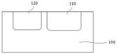
图1显示出一种本发明对比例中栅场板结构的横向功率器件,包括漂移区、沟道区、栅电极层以及位于漂移区上的场板。1 shows a lateral power device with a gate field plate structure in a comparative example of the present invention, including a drift region, a channel region, a gate electrode layer, and a field plate on the drift region.
为了不同的耐压需求,可以采用的方案是调整以下尺寸:沟道长度 a,场板与多晶硅栅之间的交叠尺寸 b,以及场板延伸出栅电极层的距离 c。以16V的LDMOS器件为例,可以采用如下的设计参数:沟道长度a在0.5um左右,场板与多晶硅栅之间的交叠尺寸 b在0.7um左右,而场板延伸出栅电极层的距离c在0.8um左右。For different withstand voltage requirements, the solution that can be used is to adjust the following dimensions: the channel length a, the overlap size b between the field plate and the polysilicon gate, and the distance c that the field plate extends beyond the gate electrode layer. Taking a 16V LDMOS device as an example, the following design parameters can be used: the channel length a is about 0.5um, the overlap size b between the field plate and the polysilicon gate is about 0.7um, and the field plate extends beyond the gate electrode layer. The distance c is about 0.8um.
然而,随着源漏耐压要求的提高, a、b、c的距离和/或尺寸需要提高,单纯的拉大以上距离,会导致芯片面积的增加,还会导致源漏的导通电阻相应的线性增加,而且距离和/或尺寸不能无限地提高。However, with the increase of source-drain withstand voltage requirements, the distance and/or size of a, b, and c need to be increased. Simply increasing the above distance will lead to an increase in the chip area, and also lead to a corresponding increase in the on-resistance of the source and drain. increases linearly, and the distance and/or size cannot be increased indefinitely.
如图1所示,LDMOS器件包括衬底100,沿横向方向设置漂移区110和沟道区120,硅局部氧化隔离区(LOCOS)201以及覆盖场板一部分的栅电极层204,其中栅场板实质上起到抑制其覆盖区域下电场的作用。常采用热氧化工艺在衬底100上形成LOCOS 201,即此处的场板,LOCOS的制备工艺存在工艺复杂、热过程多以及工艺成本高等问题,而且LOCOS会侵入Si衬底造成表面的损耗,还会影响有源区的离子注入浓度。另一方面,如图1所示的LOCOS的截面轮廓可知,LOCOS部分位于漂移区内,因此阻挡了栅极和漏极之间的电流路径,从而会产生LDMOS器件的较高导通电阻Rdson,栅场板结构的长度以及剖面进行调整可以使场板边缘的电场峰值优化以及实现耗尽区边界的曲率半径减小。As shown in FIG. 1, the LDMOS device includes a
为了解决由LOCOS场板造成的衬底损耗等问题,本发明提供了一种具有栅场板结构的横向功率器件的改进结构,所述具有栅场板结构的横向功率器件包括:第一导电类型的衬底,所述衬底沿横向方向包括沟道区和第二导电类型的漂移区;平面场板结构,设置于所述漂移区上,所述平面场板结构包括高温氧化物层;栅结构,所述栅结构包括邻接所述平面场板结构而设置于所述衬底上的栅介质层和覆盖所述平面场板结构一部分的栅电极层,所述平面场板结构的底面不低于所述栅介质层的底面;源区,位于所述沟道区中; 漏区,位于所述漂移区中;和第一金属硅化物层,设置于所述衬底的表面上。In order to solve the problems of substrate loss caused by the LOCOS field plate, the present invention provides an improved structure of a lateral power device with a grid field plate structure, and the lateral power device with a grid field plate structure includes: a first conductivity type a substrate, the substrate includes a channel region and a drift region of the second conductivity type along the lateral direction; a planar field plate structure is disposed on the drift region, and the planar field plate structure includes a high temperature oxide layer; a gate The gate structure includes a gate dielectric layer disposed on the substrate adjacent to the planar field plate structure and a gate electrode layer covering a part of the planar field plate structure, and the bottom surface of the planar field plate structure is not low on the bottom surface of the gate dielectric layer; a source region located in the channel region; a drain region located in the drift region; and a first metal silicide layer disposed on the surface of the substrate.
此后,将参照图2-图5具体描述本发明的具有栅场板结构的横向功率器件及其制备方法,制备栅场板结构的横向功率器件的各阶段的具体结构将结合图3A至3G加以说明。Hereinafter, the lateral power device with a grid field plate structure and a manufacturing method thereof of the present invention will be described in detail with reference to FIGS. 2 to 5 . The specific structures of each stage of preparing the lateral power device with a grid field plate structure will be described in conjunction with FIGS. 3A to 3G . illustrate.
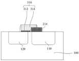
参见图2,其显示出本发明实施例中的具有栅场板结构的横向功率器件。该横向功率器件包括:衬底100,在衬底100中形成有有源区(图中未示出),沿横向方向包括漂移区110和沟道区120,漂移区110和沟道区120位于衬底100的有源区内且衬底100沿横向方向设置,漂移区110和沟道区120之间具有间距。此处,衬底100为第一导电类型可以为N型或P型,则漂移区110具有第二导电类型,该第二导电类型为与第一导电类型相反的导电类型。如图3所示,源区510和漏区520分别位于漂移区110和沟道区120内。在本实施例中,漂移区110、沟道区120、源区510和漏区520的离子注入类型可以根据所需器件的类型进行适当地调整。Referring to FIG. 2, there is shown a lateral power device having a grid field plate structure in an embodiment of the present invention. The lateral power device includes: a
该横向功率器件包括平面场板结构210和栅结构310,平面场板结构210设置于漂移区110上,栅结构310包括栅介质层312和位于该栅介质层上的栅电极层314,栅介质层312邻接平面场板结构210而设置于衬底100上,栅电极层314与平面场板结构交叠而设置于该栅介质层上,平面场板结构210的底面不低于栅介质层312的底面。参见图2,栅介质层312的底面与平面场板结构210的底面处于同一水平面,场板形成在所述漂移区的上方,即位于栅极和漏极之间的水平面上方,这样不会阻挡栅极和漏极之间的电流路径,缩短了漂移区电流路径,从而可以改善器件的性能。具体地,平面场板结构210包括高温氧化物层212,该高温氧化物层可以采用沉积工艺形成于衬底,而无需经由热氧化处理衬底,避免了热过程对衬底的损伤,同时免于有源区离子注入浓度受到影响。在一些示例中,栅电极层314为多晶硅栅,场板结构210还包括位于高温氧化物层两侧的介电侧墙214,介电侧墙214的设置有利于防止多晶硅电极的残留。作为示例,高温氧化物层212可以包括SiO2层,介电侧墙可以包括氮化硅。The lateral power device includes a planar
该横向功率器件还包括设置于衬底100表面上的第一金属硅化物层410,设置于栅电极层314上的第二金属硅化物层420。在一些示例中,栅电极层314为多晶硅栅,可以通过自对准工艺于多晶硅栅上形成的第二金属硅化物层420。具体地,该横向功率器件还包括覆盖整个有源区的层间介质层600和设置于层间介质层600上的金属布线层700。较佳地,第一金属硅化物层410与层间介质层600之间还设置有接触孔停止层800,以使通过刻蚀工艺形成的接触孔停止于第一金属硅化物层410的表面。举例而言,接触孔停止层800包含氮化硅或氮氧化硅材料,且接触孔停止层800的厚度范围为300Å~800 Å。The lateral power device further includes a first
具体地,贯穿层间介质层600和接触孔停止层800形成有多个接触孔,于所述接触孔中填充金属插塞,使得于层间介质层600中设置分别与源区510对应的源极插塞611、与漏区520对应的漏极插塞621和与平面场板结构210对应的转移插塞631,金属布线层700覆盖于层间介质层600且与层间介质层中的金属插塞电性连接。作为示例,金属布线层700包括第一金属图案和第二金属图案,所述第一金属图案分别与源极插塞611和转移插塞631电性连接,源极插塞611通过第一金属硅化物层410与源区510电性接触,所述第二金属图案与漏极插塞621电性连接,漏极插塞621通过第一金属硅化物层410与漏区520电性接触。在此种设置中,通过分别与源区和漏区接触的第一金属硅化物层410和设置于栅电极层314上的第二金属硅化物层420,实现电极与有源区之间的电性接触,以降低接触孔的孔电阻以及接触孔与半导体器件的待引出区之间电性接触的接触电阻。通过设置于转移接触孔630中的转移插塞631,转移插塞631与平面场板结构210电性接触。由于转移插塞631的存在使得在半导体器件中增加了一个零电位的耗尽点,在漏极插塞621接入高电压时,使得漂移区110中的耗尽层的宽度增加,能够提高半导体器件的耐压,且不会形成较大的导通电阻,从而实现提高半导体器件的电性能。作为示例,转移接触孔630具有介于0.35um~0.6um的横向尺寸。Specifically, a plurality of contact holes are formed through the
在本实施例中,所述横向功率器件可以包括横向双扩散金属氧化物晶体管(LDMOS)。In this embodiment, the lateral power device may include a lateral double diffused metal oxide transistor (LDMOS).
参阅图3及图5,本实施例还提供一种具有栅场板结构的横向功率器件的制备方法,可采用以下详述的制备方法制备本发明的具有栅场板结构的横向功率器件,但所述横向功率器件的制备方法局限于本实施例描述的具体材质及工艺步骤,在不背离本发明的发明构思的情况下能够实现以上所述横向功率器件结构的方法和/或工艺应当视为处于本发明要求保护的范围之内。Referring to FIG. 3 and FIG. 5 , this embodiment also provides a method for preparing a lateral power device with a grid field plate structure. The preparation method of the lateral power device is limited to the specific materials and process steps described in this embodiment, and the method and/or process that can realize the above-mentioned lateral power device structure without departing from the inventive concept of the present invention should be regarded as within the scope of the claimed invention.
参见图3A,步骤1),提供一衬底,以及于所述衬底形成漂移区和沟道区。可以通过交替地执行光刻工艺和离子注入工艺以达成漂移区110和沟道区120的离子注入,随后执行阱推进和退火工艺于衬底内形成所需导电类型的漂移区和沟道区,其中衬底具有第一导电类型,漂移区可以具有与衬底的第一导电类型相反的第二导电类型。可以采用本领域常规使用的设备和/或工艺参数形成所述漂移区和沟道区,相关工艺的具体细节在此不作赘述。Referring to FIG. 3A , step 1), a substrate is provided, and a drift region and a channel region are formed on the substrate. The ion implantation of the
接着,进行步骤2),于衬底上形成平面场板结构。具体地,形成平面场板结构210的步骤可以包括:于所述衬底上沉积高温氧化物(HTO);对高温氧化物进行刻蚀,去除位于所述衬底的预定区域上的高温氧化物,以得到设置于漂移区110上的高温氧化物层212。作为示例,可以通过化学气相沉积(CVD)工艺和等离子体增强化学气相沉积(PECVD)工艺或类似沉积工艺形成所述高温氧化物,以及通过光刻工艺和湿法刻蚀工艺对所述高温氧化物进行刻蚀,其中在高温氧化物的光刻工艺中关键尺寸可达0.35微米。较佳地,高温氧化物可以包含SiO2,沉积的高温氧化物的厚度范围为800Å~1200 Å,可以通过湿法刻蚀工艺采用对SiO2具有高选择比的化学腐蚀液进行刻蚀,湿法腐蚀液例如是H3PO4溶液。Next, step 2) is performed to form a planar field plate structure on the substrate. Specifically, the steps of forming the planar
进一步地,形成平面场板结构210的步骤还包括沉积介电材料以形成包围所述高温氧化物层的介电层;以及通过干法刻蚀工艺对高温氧化物层212顶部的介电材料层进行各向异性地刻蚀,以形成高温氧化物层212的介电侧墙214,如图3B所示,其中该介电侧墙214可以防止后续的多晶硅刻蚀的残留。具体地,刻蚀气体例如Cl2和CF4,由于在高温氧化物层两边的介电材料在垂直方向较厚,在刻蚀相同厚度的情况下,拐角处的一些介电材料不能被刻蚀,由此形成介电侧墙。在本实施例中,介电材料层可以保形地沉积于高温氧化物层212的顶部和侧面,其中所述介电材料层包括氮化硅层,沉积的所述氮化硅层的厚度范围为300Å~500 Å。Further, the step of forming the planar
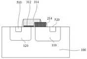
参见图3C,步骤3),于所述衬底上形成栅结构。具体地,形成所述栅结构的步骤可以包括:邻接平面场板结构210而于衬底100上形成栅介质层312;以及于栅介质层312上形成栅电极层314。举例而言,栅介质层312为栅氧层,栅电极层314为多晶硅栅,所述栅氧层可以通过CVD工艺沉积或热氧化工艺形成。在进行栅氧材料的沉积工艺之前,可以对衬底100的表面预清洗,以防止杂质影响氧化物形成的质量;随后可以于衬底100的表面沉积栅氧材料层。具体地,可以通过光刻工艺将栅极掩膜版上的图案套刻到衬底表面的栅氧材料层,通过刻蚀工艺显露出凹槽,于凹槽底部的栅氧材料上形成多晶硅栅。Referring to FIG. 3C, step 3), a gate structure is formed on the substrate. Specifically, the steps of forming the gate structure may include: forming a
步骤4),于所述沟道区内设置形成源区,以及于所述漂移区内形成漏区。作为示例,参见图3D,可以根据套刻的硬掩膜版通过离子注入工艺于漂移区110内形成漏区520,以及于沟道区120内形成源区510。具体地,可以通过微影技术和离子注入工艺依次形成源区510和漏区520,可以采用本领域常规使用的设备和/或工艺参数形成所述源区和漏区,相关工艺的具体细节在此不作赘述。可选地,在形成源区510和漏区520,可以执行快速热退火以修复离子注入造成的硅表面晶体损伤,激活离子注入的杂质。Step 4), forming a source region in the channel region, and forming a drain region in the drift region. As an example, referring to FIG. 3D , a
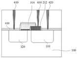
随后,进行步骤5),于所述衬底的表面形成第一金属硅化物层。具体地,参见图3E,通过自对准工艺于所述衬底上形成第一金属硅化物层410,在栅电极层314为多晶硅栅的示例中,可以通过自对准工艺在形成第一金属硅化物层410的同时于多晶硅栅上形成第二金属硅化物层420。由于该步骤采用自对准工艺,可以使用前一工序的掩膜。举例而言,第一金属硅化物层410和第二金属硅化物层420可以为低阻的金属硅化物TiSi2。Then, step 5) is performed to form a first metal silicide layer on the surface of the substrate. Specifically, referring to FIG. 3E , a first
步骤6),形成层间介质层以及实现电性连接。可选地,在形成第一金属硅化物层410之后,所述制备方法还包括于第一金属硅化物层410和平面场板结构的裸露部分上沉积接触孔停止层800,所述接触孔停止层包含氮化硅或氮氧化硅材料。具体地,形成层间介质层600的步骤之后,于该层间介质层内形成多个接触孔,包括:根据光刻定义的图形区域进行刻蚀以形成贯穿层间介质层600和接触孔停止层800的源极接触孔610和漏极接触孔620,上述刻蚀工艺停止于第一金属硅化物410上,如图3F所示;在该工序中,第一金属硅化物的耗尽量可达100Å~400Å。在本实施例中,于形成源极插塞611和漏极插塞621的同时形成转移插塞631,包括:根据光刻定义的图案进行刻蚀以贯穿层间介质层600形成转移接触孔630,其中转移接触孔630底部显露出平面场板结构210,所述转移接触孔具有在0.35μm~0.6μm范围内的横向尺寸。随后,通过涂覆工艺于多个接触孔中填充金属,以形成金属插塞,如图3G所示。所述涂覆工艺可以包括电镀工艺、物理气相沉积、化学气相沉积或其他沉积工艺。Step 6), forming an interlayer dielectric layer and realizing electrical connection. Optionally, after the first
于步骤7),对本实施例和对比例的LDMOS器件的静态特性参数进行仿真分析,图4A和4B显示出TCAD内仿真出的LDMOS器件结构及其对应的LDMOS器件源漏击穿电压的状态下电势分布图,由图4A和4B可知,在本实施例中LDMOS器件的场板覆盖区域内电势分布变化平缓,电场分布较为均匀,相较于对比例的LDMOS器件,本实施例中器件的耗尽区边界的曲率半径明显减小。结合图5的图表可知,本实施例与对比例的LDMOS器件具有的击穿电压值接近,而与对比例的LDMOS器件相比本发明的实施例中的源漏导通电阻RSPon 明显降低。具体地,如图5的图表所示的仿真测试显示,对比例的LDMOS器件Rdson为8.7 mΩ·mm-2,而本实施例中Rdson为8.2mΩ·mm-2;即,本实施例在击穿电压略有提升(32V)的情况下,导通电压明显降低。In step 7), the static characteristic parameters of the LDMOS device of the present embodiment and the comparative example are simulated and analyzed. Figures 4A and 4B show the LDMOS device structure simulated in TCAD and the state of the source-drain breakdown voltage of the corresponding LDMOS device. It can be seen from Figures 4A and 4B that the potential distribution in the field plate coverage area of the LDMOS device in this embodiment changes gently, and the electric field distribution is relatively uniform. Compared with the LDMOS device of the comparative example, the power consumption of the device in this embodiment is The radius of curvature of the exhaust boundary is significantly reduced. 5 , it can be seen that the LDMOS device of the present embodiment and the comparative example have similar breakdown voltage values, and compared with the LDMOS device of the comparative example, the source-drain on-resistance RSPon of the embodiment of the present invention is significantly lower. Specifically, the simulation test shown in the graph of FIG. 5 shows that the Rdson of the LDMOS device of the comparative example is 8.7 mΩ·mm−2 , while the Rdson of the present embodiment is 8.2 mΩ·mm−2 ; that is, the present embodiment With a slight increase in breakdown voltage (32V), the on-voltage is significantly reduced.
综上所述,本发明提供的具有栅场板结构的横向功率器件及其制备方法,具有以下有益效果:To sum up, the lateral power device with the grid field plate structure and the preparation method thereof provided by the present invention have the following beneficial effects:
本发明提供的所述横向功率器件中,平面场板结构的底面不低于栅介质层的底面,且具有平缓的剖面,使得场板覆盖区域内电势分布变得平缓;还避免了有源区的离子注入浓度受到的影响,有利于提高器件的质量。In the lateral power device provided by the present invention, the bottom surface of the planar field plate structure is not lower than the bottom surface of the gate dielectric layer, and has a gentle cross section, so that the potential distribution in the coverage area of the field plate becomes smooth; and the active area is avoided. The ion implantation concentration is affected, which is beneficial to improve the quality of the device.
本发明提供的具有栅场板结构的横向功率器件的制备方法中,通过沉积工艺于衬底表面形成平面场板结构,而无需硅衬底的热氧化工艺,避免了对衬底表面侵入及其造成的损伤,所述制备方法具有工艺简单、可操作性强等优势。In the preparation method of the lateral power device with the gate field plate structure provided by the present invention, the planar field plate structure is formed on the surface of the substrate through the deposition process, without the thermal oxidation process of the silicon substrate, and the invasion of the surface of the substrate and its impact are avoided. The said preparation method has the advantages of simple process, strong operability and the like.
所以,本发明有效克服了现有技术中的种种缺点而具高度产业利用价值。Therefore, the present invention effectively overcomes various shortcomings in the prior art and has high industrial utilization value.
上述实施例仅例示性说明本发明的原理及其功效,而非用于限制本发明。任何熟悉此技术的人士皆可在不违背本发明的精神及范畴下,对上述实施例进行修饰或改变。因此,举凡所属技术领域中具有通常知识者在未脱离本发明所揭示的精神与技术思想下所完成的一切等效修饰或改变,仍应由本发明的权利要求所涵盖。The above-mentioned embodiments merely illustrate the principles and effects of the present invention, but are not intended to limit the present invention. Anyone skilled in the art can modify or change the above embodiments without departing from the spirit and scope of the present invention. Therefore, all equivalent modifications or changes made by those with ordinary knowledge in the technical field without departing from the spirit and technical idea disclosed in the present invention should still be covered by the claims of the present invention.
Claims (14)
Priority Applications (1)
| Application Number | Priority Date | Filing Date | Title |
|---|---|---|---|
| CN202210357476.5ACN114429985B (en) | 2022-04-07 | 2022-04-07 | Transverse power device with grid field plate structure and preparation method thereof |
Applications Claiming Priority (1)
| Application Number | Priority Date | Filing Date | Title |
|---|---|---|---|
| CN202210357476.5ACN114429985B (en) | 2022-04-07 | 2022-04-07 | Transverse power device with grid field plate structure and preparation method thereof |
Publications (2)
| Publication Number | Publication Date |
|---|---|
| CN114429985Atrue CN114429985A (en) | 2022-05-03 |
| CN114429985B CN114429985B (en) | 2022-06-21 |
Family
ID=81314308
Family Applications (1)
| Application Number | Title | Priority Date | Filing Date |
|---|---|---|---|
| CN202210357476.5AActiveCN114429985B (en) | 2022-04-07 | 2022-04-07 | Transverse power device with grid field plate structure and preparation method thereof |
Country Status (1)
| Country | Link |
|---|---|
| CN (1) | CN114429985B (en) |
Cited By (1)
| Publication number | Priority date | Publication date | Assignee | Title |
|---|---|---|---|---|
| CN116959994A (en)* | 2023-09-21 | 2023-10-27 | 华南理工大学 | Preparation method of LDMOS device with double-T structure |
Citations (5)
| Publication number | Priority date | Publication date | Assignee | Title |
|---|---|---|---|---|
| US20030141559A1 (en)* | 2001-12-20 | 2003-07-31 | Stmicroelectronics S.R.I. | Metal oxide semiconductor field-effect transistor and associated methods |
| US20140319622A1 (en)* | 2013-04-25 | 2014-10-30 | Vanguard International Semiconductor Corporation | Semiconductor device and methods for forming the same |
| US20150048448A1 (en)* | 2013-08-15 | 2015-02-19 | Vanguard International Semiconductor Corporation | Semiconductor device and method for forming the same |
| CN108258051A (en)* | 2018-01-11 | 2018-07-06 | 上海华虹宏力半导体制造有限公司 | LDMOS device and its manufacturing method |
| CN113903792A (en)* | 2021-12-09 | 2022-01-07 | 广州粤芯半导体技术有限公司 | Semiconductor device and method for manufacturing the same |
- 2022
- 2022-04-07CNCN202210357476.5Apatent/CN114429985B/enactiveActive
Patent Citations (5)
| Publication number | Priority date | Publication date | Assignee | Title |
|---|---|---|---|---|
| US20030141559A1 (en)* | 2001-12-20 | 2003-07-31 | Stmicroelectronics S.R.I. | Metal oxide semiconductor field-effect transistor and associated methods |
| US20140319622A1 (en)* | 2013-04-25 | 2014-10-30 | Vanguard International Semiconductor Corporation | Semiconductor device and methods for forming the same |
| US20150048448A1 (en)* | 2013-08-15 | 2015-02-19 | Vanguard International Semiconductor Corporation | Semiconductor device and method for forming the same |
| CN108258051A (en)* | 2018-01-11 | 2018-07-06 | 上海华虹宏力半导体制造有限公司 | LDMOS device and its manufacturing method |
| CN113903792A (en)* | 2021-12-09 | 2022-01-07 | 广州粤芯半导体技术有限公司 | Semiconductor device and method for manufacturing the same |
Cited By (2)
| Publication number | Priority date | Publication date | Assignee | Title |
|---|---|---|---|---|
| CN116959994A (en)* | 2023-09-21 | 2023-10-27 | 华南理工大学 | Preparation method of LDMOS device with double-T structure |
| CN116959994B (en)* | 2023-09-21 | 2023-12-29 | 华南理工大学 | Preparation method of LDMOS device with double T structure |
Also Published As
| Publication number | Publication date |
|---|---|
| CN114429985B (en) | 2022-06-21 |
Similar Documents
| Publication | Publication Date | Title |
|---|---|---|
| KR101070845B1 (en) | Method for forming structures in finfet devices | |
| CN103928514B (en) | Power mosfet and forming method thereof | |
| TWI462295B (en) | Ditch type power transistor component and manufacturing method thereof | |
| TWI407564B (en) | Power semiconductor having trench bottom polycrystalline germanium structure and method of fabricating the same | |
| TWI515893B (en) | Vertical power MOS half field effect transistor and forming method thereof | |
| CN111554578B (en) | Semiconductor structure and forming method thereof | |
| CN115642182B (en) | Transverse double-diffusion field effect transistor, manufacturing method, chip and circuit | |
| CN104638011B (en) | A kind of groove MOSFET device and preparation method thereof | |
| CN109585558B (en) | LDMOS FINFET structure with multiple gate structures | |
| CN112018187A (en) | LDMOS device and manufacturing method thereof | |
| CN114429985B (en) | Transverse power device with grid field plate structure and preparation method thereof | |
| CN101916783B (en) | Transverse and longitudinal diffusion type field effect transistor of depressed channel and manufacturing method thereof | |
| CN114823345A (en) | LDMOS transistor and manufacturing method thereof | |
| CN109004030B (en) | Groove type MOS device structure and manufacturing method thereof | |
| CN113241375B (en) | Semiconductor device and method of manufacturing the same | |
| CN115332350A (en) | A kind of LDMOS device and preparation method thereof | |
| CN111863949B (en) | Semiconductor element and manufacturing method thereof | |
| CN114823841A (en) | Semiconductor structure and forming method thereof | |
| TWI548090B (en) | Semiconductor device and method of fabricating the same | |
| CN101621072A (en) | Semiconductor device and method for manufacturing the same | |
| TWI893321B (en) | Semiconductor device and manufacturing method thereof | |
| CN119153523B (en) | Lateral double diffused field effect transistor, manufacturing method, chip and circuit | |
| TWI897312B (en) | Power semiconductor device and manufacturing method of the same | |
| CN104218080A (en) | Radio frequency LDMOS device and manufacturing method thereof | |
| CN113380627B (en) | LDMOS transistor and forming method thereof |
Legal Events
| Date | Code | Title | Description |
|---|---|---|---|
| PB01 | Publication | ||
| PB01 | Publication | ||
| SE01 | Entry into force of request for substantive examination | ||
| SE01 | Entry into force of request for substantive examination | ||
| GR01 | Patent grant | ||
| GR01 | Patent grant | ||
| CP01 | Change in the name or title of a patent holder | ||
| CP01 | Change in the name or title of a patent holder | Address after:510700 No. 28, Fenghuang fifth road, Huangpu District, Guangzhou, Guangdong Patentee after:Yuexin Semiconductor Technology Co.,Ltd. Address before:510700 No. 28, Fenghuang fifth road, Huangpu District, Guangzhou, Guangdong Patentee before:Guangzhou Yuexin Semiconductor Technology Co.,Ltd. |