CN114420546A - Small-linewidth circular or elliptical device with controllable shape and preparation method thereof - Google Patents
Small-linewidth circular or elliptical device with controllable shape and preparation method thereofDownload PDFInfo
- Publication number
- CN114420546A CN114420546ACN202111452105.7ACN202111452105ACN114420546ACN 114420546 ACN114420546 ACN 114420546ACN 202111452105 ACN202111452105 ACN 202111452105ACN 114420546 ACN114420546 ACN 114420546A
- Authority
- CN
- China
- Prior art keywords
- layer
- auxiliary pattern
- target
- target layer
- etched
- Prior art date
- Legal status (The legal status is an assumption and is not a legal conclusion. Google has not performed a legal analysis and makes no representation as to the accuracy of the status listed.)
- Pending
Links
- 238000002360preparation methodMethods0.000titleclaimsabstractdescription8
- 238000005530etchingMethods0.000claimsabstractdescription43
- 230000004888barrier functionEffects0.000claimsabstractdescription39
- 239000000758substrateSubstances0.000claimsabstractdescription26
- 239000000463materialSubstances0.000claimsabstractdescription21
- 238000000151depositionMethods0.000claimsabstractdescription8
- 238000001259photo etchingMethods0.000claimsabstract3
- 238000000034methodMethods0.000claimsdescription43
- WGTYBPLFGIVFAS-UHFFFAOYSA-Mtetramethylammonium hydroxideChemical compound[OH-].C[N+](C)(C)CWGTYBPLFGIVFAS-UHFFFAOYSA-M0.000claimsdescription18
- 229910052581Si3N4Inorganic materials0.000claimsdescription4
- 229910021420polycrystalline siliconInorganic materials0.000claimsdescription4
- 229920005591polysiliconPolymers0.000claimsdescription4
- HQVNEWCFYHHQES-UHFFFAOYSA-Nsilicon nitrideChemical compoundN12[Si]34N5[Si]62N3[Si]51N64HQVNEWCFYHHQES-UHFFFAOYSA-N0.000claimsdescription4
- VYPSYNLAJGMNEJ-UHFFFAOYSA-NSilicium dioxideChemical compoundO=[Si]=OVYPSYNLAJGMNEJ-UHFFFAOYSA-N0.000claimsdescription3
- 239000007769metal materialSubstances0.000claimsdescription3
- 229910052814silicon oxideInorganic materials0.000claimsdescription3
- 150000007530organic basesChemical class0.000claimsdescription2
- 125000006850spacer groupChemical group0.000description10
- 238000001459lithographyMethods0.000description6
- 238000000206photolithographyMethods0.000description6
- 230000000717retained effectEffects0.000description3
- 239000003513alkaliSubstances0.000description2
- 238000001312dry etchingMethods0.000description2
- 239000007788liquidSubstances0.000description2
- 238000010586diagramMethods0.000description1
- 238000000407epitaxyMethods0.000description1
- 238000000671immersion lithographyMethods0.000description1
- 238000004519manufacturing processMethods0.000description1
- 238000012805post-processingMethods0.000description1
- 238000012545processingMethods0.000description1
- 239000004065semiconductorSubstances0.000description1
- 229910052710siliconInorganic materials0.000description1
- 239000010703siliconSubstances0.000description1
Images


Classifications
- H—ELECTRICITY
- H01—ELECTRIC ELEMENTS
- H01L—SEMICONDUCTOR DEVICES NOT COVERED BY CLASS H10
- H01L21/00—Processes or apparatus adapted for the manufacture or treatment of semiconductor or solid state devices or of parts thereof
- H01L21/02—Manufacture or treatment of semiconductor devices or of parts thereof
- H01L21/027—Making masks on semiconductor bodies for further photolithographic processing not provided for in group H01L21/18 or H01L21/34
- H01L21/0271—Making masks on semiconductor bodies for further photolithographic processing not provided for in group H01L21/18 or H01L21/34 comprising organic layers
- H—ELECTRICITY
- H01—ELECTRIC ELEMENTS
- H01L—SEMICONDUCTOR DEVICES NOT COVERED BY CLASS H10
- H01L21/00—Processes or apparatus adapted for the manufacture or treatment of semiconductor or solid state devices or of parts thereof
- H01L21/02—Manufacture or treatment of semiconductor devices or of parts thereof
- H01L21/027—Making masks on semiconductor bodies for further photolithographic processing not provided for in group H01L21/18 or H01L21/34
- H01L21/033—Making masks on semiconductor bodies for further photolithographic processing not provided for in group H01L21/18 or H01L21/34 comprising inorganic layers
Landscapes
- Engineering & Computer Science (AREA)
- Physics & Mathematics (AREA)
- Condensed Matter Physics & Semiconductors (AREA)
- General Physics & Mathematics (AREA)
- Manufacturing & Machinery (AREA)
- Computer Hardware Design (AREA)
- Microelectronics & Electronic Packaging (AREA)
- Power Engineering (AREA)
- Chemical & Material Sciences (AREA)
- Inorganic Chemistry (AREA)
- Drying Of Semiconductors (AREA)
Abstract
Description
Translated fromChinese技术领域technical field
本发明涉及集成电路半导体制造技术领域,尤其涉及到一种小尺寸图形器件的制备方法。The invention relates to the technical field of integrated circuit semiconductor manufacturing, in particular to a preparation method of a small-sized graphic device.
背景技术Background technique
随着集成电路产业的发展,工艺尺寸不断地缩小,人们对更小尺寸(十几个nm或者几十个nm)的器件和图形的需要越来越高。这就对光刻机的要求也越来越高,不管是浸润式光刻机还是阿斯麦最新的光刻机,光刻机的成本非常高,进而会增加小线宽器件图形的流片成本。因此在不增加现有流片成本的条件情况下,能做出小尺寸的图形和器件是一件很有意义的事情。With the development of the integrated circuit industry, the process size is continuously reduced, and people have higher and higher requirements for devices and patterns of smaller size (tens of nanometers or tens of nanometers). This requires more and more lithography machines. Whether it is an immersion lithography machine or ASML's latest lithography machine, the cost of the lithography machine is very high, which will increase the tape-out of small line width device patterns. cost. Therefore, it is very meaningful to be able to make small-sized graphics and devices without increasing the cost of existing tapes.
同样伴随而来很多关于解决这个问题的想法,例如有的是用光刻机的套刻精度来实现的小线宽,但是这种实现方法对光刻机的套刻要求很高,并且套刻精度并不能达到百分之百的准确,这就对目标图形的均匀性产生了影响;还有的是把图形分开成两个图形,通过两次曝光+两次刻蚀(LELE)工艺或者采用光刻冻结然后再光刻刻蚀(LPLE)的方法制备,但是同样的这种方法也需要依靠高的套刻精度,对图形的对称性和均匀性也都会产生影响。There are also many ideas to solve this problem. For example, some small line widths are realized by the overlay accuracy of the lithography machine. However, this implementation method has high requirements for the overlay of the lithography machine, and the overlay accuracy is not high. Can not achieve 100% accuracy, which has an impact on the uniformity of the target pattern; there are also two patterns that are divided into two patterns, through the double exposure + double etch (LELE) process or the use of photolithography to freeze and then photolithography Etching (LPLE) method, but the same method also needs to rely on high overlay accuracy, which will also affect the symmetry and uniformity of the pattern.
因此,如何在目前光刻技术的前提下,能够直接有效的控制小尺寸图形的线宽,且保持后道工艺中图形的均匀性和完整性,是当前许多小尺寸图形设计者面临的问题。Therefore, under the premise of current lithography technology, how to directly and effectively control the line width of small-sized patterns and maintain the uniformity and integrity of patterns in subsequent processes is a problem faced by many small-sized pattern designers.
发明内容SUMMARY OF THE INVENTION
为了克服上述问题,本发明的目的在于提供一种能够有效控制形状的小线宽器件的制备方法,且该制备方法能够保持后道工艺中图形的均匀性和完整性。In order to overcome the above problems, the purpose of the present invention is to provide a preparation method of a device with small line width that can effectively control the shape, and the preparation method can maintain the uniformity and integrity of the pattern in the subsequent process.
为了实现上述目的,本发明提供了一种可控制形状的小线宽圆或椭圆形器件的制备方法,包括以下步骤:In order to achieve the above object, the present invention provides a method for preparing a shape-controllable small-line-width circular or elliptical device, comprising the following steps:
提供衬底材料层,在所述衬底材料层表面外延一层制备所需要的材料作为待刻蚀目标层;A substrate material layer is provided, and a layer of material required for epitaxial preparation is used as the target layer to be etched on the surface of the substrate material layer;
对待刻蚀目标层进行第一次刻蚀处理,形成第一目标层:The first etching process is performed on the target layer to be etched to form the first target layer:
在所述待刻蚀目标层上沉积一层辅助图形层,对该辅助图形层进行光刻去除多余的部分,形成第一辅助图形层;depositing an auxiliary pattern layer on the to-be-etched target layer, and performing photolithography on the auxiliary pattern layer to remove redundant parts to form a first auxiliary pattern layer;
在所述第一辅助图形层以及未被该第一辅助图形层覆盖的待刻蚀目标层表面沉积第一阻挡层;depositing a first barrier layer on the surface of the first auxiliary pattern layer and the to-be-etched target layer not covered by the first auxiliary pattern layer;
用刻蚀工艺将所述水平方向的第一阻挡层去除,只保留第一辅助图形层两侧竖直方向的第一阻挡层;removing the first barrier layer in the horizontal direction by an etching process, leaving only the first barrier layer in the vertical direction on both sides of the first auxiliary pattern layer;
腐蚀去掉所述第一辅助图形层,留下两侧竖直方向的第一阻挡层作为第一侧墙层;Etching and removing the first auxiliary pattern layer, leaving the first barrier layer in the vertical direction on both sides as the first sidewall layer;
以所述第一侧墙层作为硬掩模进行刻蚀,除去衬底上多余的待刻蚀目标层,只保留第一侧墙层下方的待刻蚀目标层;Etching with the first sidewall layer as a hard mask, removing the redundant target layer to be etched on the substrate, and only retaining the target layer to be etched below the first sidewall layer;
腐蚀掉所述第一侧墙层,在衬底上留下的待刻蚀目标层作为第一目标层;Etching off the first spacer layer, and leaving the target layer to be etched on the substrate as the first target layer;
对所述第一目标层进行第二次刻蚀处理,形成第二目标层:A second etching process is performed on the first target layer to form a second target layer:
在所述衬底材料层和第一目标层表面重新沉积一层待刻蚀辅助图形层,对该辅助图形层进行光刻去除多余的部分,形成第二辅助图形层;Re-deposit a layer of auxiliary pattern layer to be etched on the surface of the substrate material layer and the first target layer, and perform photolithography on the auxiliary pattern layer to remove redundant parts to form a second auxiliary pattern layer;
在所述第二辅助图形层以及未被该第二辅助图形层覆盖的第一目标层表面沉积第二阻挡层;depositing a second barrier layer on the surface of the second auxiliary pattern layer and the first target layer not covered by the second auxiliary pattern layer;
用刻蚀工艺将所述水平方向多余的第二阻挡层去除,只保留第二辅助图形层两侧竖直方向的第二阻挡层;removing the redundant second barrier layer in the horizontal direction by an etching process, and only retaining the second barrier layer in the vertical direction on both sides of the second auxiliary pattern layer;
腐蚀去掉所述第二辅助图形层,留下两侧竖直方向的第二阻挡层作为第二侧墙层;Etching and removing the second auxiliary pattern layer, leaving the second barrier layer in the vertical direction on both sides as the second sidewall layer;
以所述第二侧墙层作为硬掩模进行刻蚀,除去衬底上多余的第一目标层,只保留第二侧墙层下方的第一目标层;Etching with the second spacer layer as a hard mask, removing the redundant first target layer on the substrate, and leaving only the first target layer below the second spacer layer;
腐蚀掉所述第二侧墙层,在衬底上留下的第一目标层作为第二目标层;Etching off the second spacer layer, leaving the first target layer on the substrate as the second target layer;
通过所述二次刻蚀处理后,对衬底上的第二目标层进行刻蚀去除多余的棱角,最终形成小线宽圆或椭圆形的器件。After the second etching process, the second target layer on the substrate is etched to remove excess edges and corners, and finally a circular or elliptical device with a small line width is formed.
作为进一步的优选,所述待刻蚀目标层为金属材料。As a further preference, the target layer to be etched is a metal material.
作为进一步的优选,所述第一、第二辅助图形层都是多晶硅。As a further preference, the first and second auxiliary pattern layers are both polysilicon.
作为进一步的优选,所述第一、第二阻挡层可以是氧化硅或氮化硅。As a further preference, the first and second barrier layers may be silicon oxide or silicon nitride.
作为进一步的优选,所述用于腐蚀第一、第二辅助图形层的有机碱是四甲基氢氧化铵溶液。As a further preference, the organic base used for etching the first and second auxiliary pattern layers is tetramethylammonium hydroxide solution.
作为进一步的优选,所述形成的第二辅助图形层和第二侧墙层都与第一目标层相互垂直形成90°夹角。As a further preference, both the formed second auxiliary pattern layer and the second sidewall layer are perpendicular to the first target layer to form an included angle of 90°.
作为进一步的优选,所述形成的第二侧墙层与第一目标层相互垂直形成90°夹角。As a further preference, the formed second sidewall layer and the first target layer are perpendicular to each other to form an included angle of 90°.
作为进一步的优选,所述用于腐蚀第一、第二侧墙层的是KOH溶液。As a further preference, the KOH solution is used for etching the first and second sidewall layers.
作为进一步的优选,所述最终形成小线宽圆或椭圆形器件的大小、形状以及位置,可以通过调节第一、第二侧墙层的宽度和位置来控制。As a further preference, the size, shape and position of the small line width circular or elliptical device can be controlled by adjusting the width and position of the first and second sidewall layers.
作为进一步的优选,所述的第一、第二侧墙层的宽度和位置,可以通过调节第一、第二辅助图形层的形状,以及在其表面沉积的阻挡层的厚度来控制。As a further preference, the widths and positions of the first and second sidewall layers can be controlled by adjusting the shapes of the first and second auxiliary graphic layers and the thickness of the barrier layer deposited on the surfaces thereof.
所述的一种可控制形状的小线宽圆或椭圆形器件,由上面所述的方法制备而成。The shape-controllable small-line-width circular or elliptical device is prepared by the method described above.
本发明采用两次垂直交叉的侧墙来当硬掩模,通过两次刻蚀的方法,最终经过后续处理以后得到小线宽的圆形或者椭圆形器件。该方法制备的图形均匀性好、完整性高,不用受制于套刻精度的限制,并且可以根据改变不同侧墙的尺寸来控制圆形或者椭圆形的线宽形状,同时这种方法基本能够满足大多数做小尺寸器件者的工艺需求,可以支持推广。In the present invention, two vertically intersecting sidewalls are used as hard masks, and a circular or elliptical device with a small line width is finally obtained after subsequent processing by means of two etchings. The pattern prepared by this method has good uniformity and high integrity, and is not limited by the overlay accuracy, and can control the circular or elliptical line width shape according to changing the size of different side walls. At the same time, this method can basically satisfy the The process requirements of most small-sized device manufacturers can support promotion.
附图说明Description of drawings
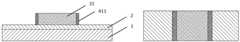
图1是形成第一辅助图形层后的前视图(左)和俯视图(右);1 is a front view (left) and a top view (right) after forming the first auxiliary graphic layer;
图2是形成第一阻挡层后的前视图(左)和俯视图示意图(右);Figure 2 is a front view (left) and a schematic top view (right) after forming the first barrier layer;
图3是形成第一侧墙层后的前视图(左)和俯视图(右);3 is a front view (left) and a top view (right) after forming the first sidewall layer;
图4是去掉第一辅助图形层后的前视图(左)和俯视图(右);4 is a front view (left) and a top view (right) after removing the first auxiliary graphics layer;
图5是形成第一目标层后的前视图(左)和俯视图(右);5 is a front view (left) and a top view (right) after forming the first target layer;
图6是去掉第一侧墙层后的前视图(左)和俯视图(右);Figure 6 is a front view (left) and a top view (right) after removing the first sidewall layer;
图7是重新生长辅助图形后的前视图(左)和俯视图(右);Figure 7 is a front view (left) and a top view (right) after regrowing the auxiliary pattern;
图8是形成第二辅助图形层后的左视图(左)和俯视图(右);8 is a left view (left) and a top view (right) after forming the second auxiliary graphics layer;
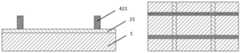
图9是形成第二阻挡层后的前视图(左)和俯视图(右);9 is a front view (left) and a top view (right) after forming the second barrier layer;
图10是形成第二侧墙层后的前视图(左)和俯视图(右);Figure 10 is a front view (left) and a top view (right) after forming the second sidewall layer;
图11是去掉第二辅助图形层后的前视图(左)和俯视图(右);Figure 11 is a front view (left) and a top view (right) after removing the second auxiliary graphics layer;
图12是形成第二目标层后的前视图(左)和俯视图(右);12 is a front view (left) and a top view (right) after forming the second target layer;
图13是去掉第二侧墙层后的前视图(左)和俯视图(右);Figure 13 is a front view (left) and a top view (right) after removing the second sidewall layer;
图14是经过后处理后形成的器件形貌示意图;Figure 14 is a schematic diagram of the morphology of the device formed after post-processing;
图中1-衬底材料层,2-待刻蚀目标层,21-第一目标层,22-第二目标层,3-待刻蚀辅助图形层,31-第一辅助图形层,32-第二辅助图形层,41-第一阻挡层,42-第二阻挡层,411-第一侧墙层,421-第二侧墙层。In the figure, 1-substrate material layer, 2-target layer to be etched, 21-first target layer, 22-second target layer, 3-auxiliary pattern layer to be etched, 31-first auxiliary pattern layer, 32- The second auxiliary pattern layer, 41-first barrier layer, 42-second barrier layer, 411-first sidewall layer, 421-second sidewall layer.
具体实施方式Detailed ways
为使本发明的上述目的、特征和优点能够更为明显易懂,下面结合附图对本发明的具体实施例做详细的说明。In order to make the above objects, features and advantages of the present invention more clearly understood, the specific embodiments of the present invention will be described in detail below with reference to the accompanying drawings.
在本发明的描述中,需要理解的是,术语“上”、“下”、“前”“后”等指示的方位或位置关系为基于附图所示的方位或位置关系,仅是为了便于描述本发明和简化描述,而不是指示或暗示所指的装置或元件必须具有特定的方位、以特定的方位构造和操作,因此不能理解为对本发明的限制。In the description of the present invention, it should be understood that the orientation or positional relationship indicated by the terms "upper", "lower", "front", "rear", etc. is based on the orientation or positional relationship shown in the accompanying drawings, and is only for convenience The invention is described and simplified without indicating or implying that the device or element referred to must have a particular orientation, be constructed and operate in a particular orientation, and therefore should not be construed as limiting the invention.
术语“第一”、“第二”仅用于描述目的,而不能理解为指示或暗示相对重要性或者隐含指明所指示的技术特征的数量。由此,限定有“第一”、“第二”的特征可以明示或者隐含地包括至少一个该特征。The terms "first" and "second" are only used for descriptive purposes, and should not be construed as indicating or implying relative importance or implicitly indicating the number of technical features indicated. Thus, a feature delimited with "first", "second" may expressly or implicitly include at least one of that feature.
具体实施例1Specific Example 1
在提供的衬底材料层1表面外延一层制备所需要的材料作为待刻蚀目标层,具体在本实施例中,该待刻蚀目标层选用金属材料。On the surface of the provided
对待刻蚀目标层进行第一次刻蚀处理,形成第一目标层21:A first etching process is performed on the target layer to be etched to form a first target layer 21:
在所述待刻蚀目标层2上沉积一层辅助图形层,该辅助图形层所用的材料为多晶硅。An auxiliary pattern layer is deposited on the to-
结合图1所示,用四甲基氢氧化铵溶液对该辅助图形层进行光刻去除多余的部分,留下所需部分的辅助图形层作为第一辅助图形层31,通过调节该第一辅助图形层31的形状来。As shown in FIG. 1, the auxiliary pattern layer is removed by photolithography with tetramethyl ammonium hydroxide solution, and the required part of the auxiliary pattern layer is left as the first
结合图2所示,在所述第一辅助图形层31以及未被该第一辅助图形层31覆盖的待刻蚀目标层2表面沉积第一阻挡层41,该第一阻挡层41所用材料可以是氧化硅或氮化硅。As shown in FIG. 2 , a
结合图3所示,采用干法刻蚀工艺,将所述水平方向的第一辅助图形层31以及未被该第一辅助图形层31覆盖的待刻蚀目标层2表面的第一阻挡层41去除,只保留第一辅助图形层31两侧竖直方向的第一阻挡层41。As shown in FIG. 3 , a dry etching process is used to remove the first
结合图4所示,用有机碱四甲基氢氧化铵溶液腐蚀掉第一辅助图形层31,留下两侧竖直方向的第一阻挡层41作为第一侧墙层411;该过程中使用的四甲基氢氧化铵溶液只会腐蚀辅助图形层,而不会腐蚀竖直方向的第一阻挡层41。As shown in FIG. 4 , the first
结合图5所示,以所述第一侧墙层411作为硬掩模进行刻蚀,除去衬底上多余的待刻蚀目标层2,只保留第一侧墙层411下方的待刻蚀目标层2。As shown in FIG. 5 , etching is performed using the
结合图6所示,用碱性液体KOH溶液腐蚀去掉上述第一侧墙层411,在衬底上留下的待刻蚀目标层2作为第一目标层21;由于侧墙层与目标层材料对KOH溶液具有高选择比特性,在该腐蚀过程只会腐蚀掉第一侧墙层411,而不会同时腐蚀第一目标层21;6, the above-mentioned
在所述的第一次刻蚀处理过程中,可以通过调节第一辅助图形层31的形状和位置来控制第一目标层21在衬层材料层上的位置;可以通过调节沉积第一阻挡层41的厚度来控制第一目标层21的宽度。During the first etching process, the position of the
对所述第一目标层21进行第二次刻蚀处理,形成第二目标层22:A second etching process is performed on the
结合图7所示,在所述衬底材料层1和第一目标层21表面重新沉积一层待刻蚀辅助图形层3,该待刻蚀辅助图形层材料也是多晶硅。Referring to FIG. 7 , a layer of
结合图8所示,用四甲基氢氧化铵溶液光刻去除该辅助图形层余多的部分,形成第二辅助图形层;该过程形成的第二辅助图形层32与第一次刻蚀处理后形成的第一目标层21相互垂直形成90°夹角。As shown in FIG. 8 , the excess part of the auxiliary pattern layer is removed by photolithography with tetramethyl ammonium hydroxide solution to form a second auxiliary pattern layer; the second
结合图9所示,在所述第二辅助图形层32以及未被该第二辅助图形层32覆盖的第一目标层21表面沉积第二阻挡层42,该第二阻挡层所用材料可以是氧化硅或氮化硅。Referring to FIG. 9, a
结合图10所示,采用干法刻蚀工艺,将所述水平方向多余的第二辅助图形层32去除,只保留第二辅助图形层31两侧竖直方向的第二阻挡层42;As shown in FIG. 10 , a dry etching process is used to remove the redundant second
结合图11所示,用有机碱四甲基氢氧化铵溶液腐蚀掉第二辅助图形层32,留下两侧竖直方向的第二阻挡层42作为第二侧墙层421;该过程中使用的四甲基氢氧化铵溶液只会腐蚀辅助图形层,而不会腐蚀竖直方向的第二阻挡层42;所述形成的第二侧墙层42与第一目标层21相互垂直形成90°夹角。As shown in FIG. 11 , the second
结合图12所示,以所述第二侧墙层421作为硬掩模进行刻蚀,除去衬底上多余的第一目标层21,只保留第二侧墙层421下方的第一目标层21。As shown in FIG. 12 , etching is performed using the
结合图13所示,用碱性液体KOH溶液腐蚀去掉上述第二侧墙层421,在衬底上留下的第二侧墙层421下方的第一目标层21作为第二目标层22;由于侧墙层与目标层材料对KOH溶液具有高选择比特性,在该腐蚀过程只会腐蚀掉第二侧墙层421,而不会同时腐蚀第二目标层22。13, the above-mentioned
在所述的第二次刻蚀处理过程中,可以通过调节第二辅助图形层32的形状和位置来控制第二目标层22在衬层材料层上的位置;可以通过调节沉积第二阻挡层42的厚度来控制第二目标层22的形状。During the second etching process, the position of the
通过所述二次刻蚀处理后,结合图14所示,对衬底上的第二目标层22进行刻蚀去除多余的棱角,最终形成小线宽圆或椭圆形的器件。After the second etching process, as shown in FIG. 14 , the
以上仅为本发明较佳的实施例,并非因此限制本发明的实施方式及保护范围,对于本领域技术人员而言,应当能够意识到凡运用本发明说明书及图示内容所作出的等同替换和显而易见的变化所得到的方案,均应当包含在本发明的保护范围内。The above are only preferred embodiments of the present invention, and are not intended to limit the embodiments and protection scope of the present invention. For those skilled in the art, they should be aware of the equivalent replacement and Solutions obtained by obvious changes shall all be included in the protection scope of the present invention.
Claims (10)
Priority Applications (1)
| Application Number | Priority Date | Filing Date | Title |
|---|---|---|---|
| CN202111452105.7ACN114420546A (en) | 2021-12-01 | 2021-12-01 | Small-linewidth circular or elliptical device with controllable shape and preparation method thereof |
Applications Claiming Priority (1)
| Application Number | Priority Date | Filing Date | Title |
|---|---|---|---|
| CN202111452105.7ACN114420546A (en) | 2021-12-01 | 2021-12-01 | Small-linewidth circular or elliptical device with controllable shape and preparation method thereof |
Publications (1)
| Publication Number | Publication Date |
|---|---|
| CN114420546Atrue CN114420546A (en) | 2022-04-29 |
Family
ID=81264727
Family Applications (1)
| Application Number | Title | Priority Date | Filing Date |
|---|---|---|---|
| CN202111452105.7APendingCN114420546A (en) | 2021-12-01 | 2021-12-01 | Small-linewidth circular or elliptical device with controllable shape and preparation method thereof |
Country Status (1)
| Country | Link |
|---|---|
| CN (1) | CN114420546A (en) |
Citations (3)
| Publication number | Priority date | Publication date | Assignee | Title |
|---|---|---|---|---|
| US20060211260A1 (en)* | 2005-03-15 | 2006-09-21 | Luan Tran | Pitch reduced patterns relative to photolithography features |
| CN104022022A (en)* | 2013-02-28 | 2014-09-03 | 中芯国际集成电路制造(上海)有限公司 | Forming method of multigraph |
| CN105470137A (en)* | 2014-09-12 | 2016-04-06 | 中国科学院微电子研究所 | A fin etching method |
- 2021
- 2021-12-01CNCN202111452105.7Apatent/CN114420546A/enactivePending
Patent Citations (3)
| Publication number | Priority date | Publication date | Assignee | Title |
|---|---|---|---|---|
| US20060211260A1 (en)* | 2005-03-15 | 2006-09-21 | Luan Tran | Pitch reduced patterns relative to photolithography features |
| CN104022022A (en)* | 2013-02-28 | 2014-09-03 | 中芯国际集成电路制造(上海)有限公司 | Forming method of multigraph |
| CN105470137A (en)* | 2014-09-12 | 2016-04-06 | 中国科学院微电子研究所 | A fin etching method |
Similar Documents
| Publication | Publication Date | Title |
|---|---|---|
| US10768526B2 (en) | Method of forming patterns | |
| CN112864094B (en) | Semiconductor structure and method for forming the same | |
| CN111986983B (en) | Semiconductor structure and forming method thereof | |
| CN114203628A (en) | Method for manufacturing semiconductor structure | |
| CN113394198A (en) | Photoetching alignment mark and forming method thereof | |
| CN110690197A (en) | Semiconductor alignment structure and semiconductor substrate | |
| CN102446704A (en) | Dual patterning method | |
| CN207765451U (en) | A wafer structure in a photolithography process | |
| CN112017970B (en) | Manufacturing method of self-aligned metal layer, semiconductor device and electronic device | |
| JP2001312045A (en) | Method of forming mask | |
| CN114420546A (en) | Small-linewidth circular or elliptical device with controllable shape and preparation method thereof | |
| CN107785242B (en) | Triple patterning method | |
| CN209785878U (en) | Graphical mask layer and memory | |
| CN114864385A (en) | Wafer processing method | |
| CN114496741B (en) | Method for forming semiconductor structure | |
| CN112071744A (en) | Graphical mask layer and forming method thereof, memory and forming method thereof | |
| CN112992784B (en) | Semiconductor structures and methods of forming them | |
| CN112786436B (en) | Semiconductor structure and method for forming the same | |
| CN114843173A (en) | Method for forming semiconductor structure | |
| CN116206969A (en) | Semiconductor structure manufacturing method and semiconductor structure | |
| CN100399538C (en) | Method for Reducing Wafer Damage Caused by Shallow Trench Isolation Chemical Mechanical Polishing Process | |
| TW202040642A (en) | Methods for reducing transfer pattern defects and for minimizing device defects | |
| CN114200796B (en) | Alignment mark and forming method thereof | |
| CN115458507B (en) | Alignment mark and forming method thereof | |
| CN117038446B (en) | Semiconductor device, manufacturing method and device |
Legal Events
| Date | Code | Title | Description |
|---|---|---|---|
| PB01 | Publication | ||
| PB01 | Publication | ||
| SE01 | Entry into force of request for substantive examination | ||
| SE01 | Entry into force of request for substantive examination | ||
| TA01 | Transfer of patent application right | ||
| TA01 | Transfer of patent application right | Effective date of registration:20231227 Address after:Room 1605, Building 1, No. 117 Yingshan Red Road, Huangdao District, Qingdao City, Shandong Province, 266400 Applicant after:Qingdao Haicun Microelectronics Co.,Ltd. Address before:100191 rooms 504a and 504b, 5th floor, 23 Zhichun Road, Haidian District, Beijing Applicant before:Zhizhen storage (Beijing) Technology Co.,Ltd. |