CN114410302B - Near infrared fluorescent powder and optical device thereof - Google Patents
Near infrared fluorescent powder and optical device thereofDownload PDFInfo
- Publication number
- CN114410302B CN114410302BCN202111539257.0ACN202111539257ACN114410302BCN 114410302 BCN114410302 BCN 114410302BCN 202111539257 ACN202111539257 ACN 202111539257ACN 114410302 BCN114410302 BCN 114410302B
- Authority
- CN
- China
- Prior art keywords
- phosphor
- light
- infrared
- emission
- near infrared
- Prior art date
- Legal status (The legal status is an assumption and is not a legal conclusion. Google has not performed a legal analysis and makes no representation as to the accuracy of the status listed.)
- Active
Links
- 239000000843powderSubstances0.000titleclaimsabstract6
- 230000003287optical effectEffects0.000titleabstractdescription23
- OAICVXFJPJFONN-UHFFFAOYSA-NPhosphorusChemical compound[P]OAICVXFJPJFONN-UHFFFAOYSA-N0.000claimsabstractdescription100
- 239000000463materialSubstances0.000claimsabstractdescription51
- 229910052791calciumInorganic materials0.000claimsdescription23
- 239000000203mixtureSubstances0.000claimsdescription22
- 239000013078crystalSubstances0.000claimsdescription14
- 229910052746lanthanumInorganic materials0.000claimsdescription13
- 239000004065semiconductorSubstances0.000claimsdescription10
- 229910052777PraseodymiumInorganic materials0.000claimsdescription8
- 150000002484inorganic compoundsChemical class0.000claimsdescription8
- 229910010272inorganic materialInorganic materials0.000claimsdescription8
- 229910052771TerbiumInorganic materials0.000claimsdescription5
- 229910052706scandiumInorganic materials0.000claimsdescription5
- 229910052797bismuthInorganic materials0.000claimsdescription4
- 238000000295emission spectrumMethods0.000abstractdescription19
- 238000001228spectrumMethods0.000abstractdescription11
- 230000003595spectral effectEffects0.000abstractdescription10
- 238000012360testing methodMethods0.000abstractdescription7
- 230000036541healthEffects0.000abstractdescription6
- 238000012372quality testingMethods0.000abstractdescription6
- XLYOFNOQVPJJNP-UHFFFAOYSA-NwaterSubstancesOXLYOFNOQVPJJNP-UHFFFAOYSA-N0.000abstractdescription6
- 230000008901benefitEffects0.000abstractdescription5
- 230000007613environmental effectEffects0.000abstract1
- 238000004020luminiscence typeMethods0.000description24
- 229910052712strontiumInorganic materials0.000description22
- 230000000694effectsEffects0.000description21
- 229910052788bariumInorganic materials0.000description19
- 229910052688GadoliniumInorganic materials0.000description18
- 230000007704transitionEffects0.000description17
- 150000002500ionsChemical class0.000description16
- 229910052765LutetiumInorganic materials0.000description13
- 230000005284excitationEffects0.000description13
- 229910052733galliumInorganic materials0.000description13
- 229910052782aluminiumInorganic materials0.000description12
- 230000009286beneficial effectEffects0.000description12
- 230000005855radiationEffects0.000description11
- 229910052727yttriumInorganic materials0.000description11
- 230000007547defectEffects0.000description10
- 239000011159matrix materialSubstances0.000description10
- 238000011160researchMethods0.000description10
- 238000010791quenchingMethods0.000description9
- 230000000171quenching effectEffects0.000description9
- 239000000126substanceSubstances0.000description9
- 102100032047AlsinHuman genes0.000description8
- 101710187109AlsinProteins0.000description8
- 230000007423decreaseEffects0.000description8
- 239000012535impuritySubstances0.000description8
- 229910052738indiumInorganic materials0.000description8
- 229910052693EuropiumInorganic materials0.000description7
- 238000000862absorption spectrumMethods0.000description7
- 238000005090crystal fieldMethods0.000description7
- 239000003446ligandSubstances0.000description7
- 239000002994raw materialSubstances0.000description7
- 238000012546transferMethods0.000description7
- 230000006872improvementEffects0.000description6
- 229910052749magnesiumInorganic materials0.000description6
- 229910052725zincInorganic materials0.000description6
- 230000000052comparative effectEffects0.000description5
- 238000005516engineering processMethods0.000description5
- 230000008859changeEffects0.000description4
- 229910052747lanthanoidInorganic materials0.000description4
- 150000002602lanthanoidsChemical class0.000description4
- 229910052751metalInorganic materials0.000description4
- 238000001878scanning electron micrographMethods0.000description4
- 239000006104solid solutionSubstances0.000description4
- 229910005191Ga 2 O 3Inorganic materials0.000description3
- 229910052784alkaline earth metalInorganic materials0.000description3
- 238000006243chemical reactionMethods0.000description3
- 238000010586diagramMethods0.000description3
- 239000011521glassSubstances0.000description3
- 238000000034methodMethods0.000description3
- 238000012795verificationMethods0.000description3
- IJGRMHOSHXDMSA-UHFFFAOYSA-NAtomic nitrogenChemical compoundN#NIJGRMHOSHXDMSA-UHFFFAOYSA-N0.000description2
- 229910052691ErbiumInorganic materials0.000description2
- 229910052779NeodymiumInorganic materials0.000description2
- 229910003564SiAlONInorganic materials0.000description2
- 229910052769YtterbiumInorganic materials0.000description2
- 239000000654additiveSubstances0.000description2
- QVGXLLKOCUKJST-UHFFFAOYSA-Natomic oxygenChemical compound[O]QVGXLLKOCUKJST-UHFFFAOYSA-N0.000description2
- 230000033228biological regulationEffects0.000description2
- 238000009835boilingMethods0.000description2
- 229910052804chromiumInorganic materials0.000description2
- 150000001875compoundsChemical class0.000description2
- 238000001816coolingMethods0.000description2
- 238000002425crystallisationMethods0.000description2
- 230000008025crystallizationEffects0.000description2
- 238000009792diffusion processMethods0.000description2
- 238000006073displacement reactionMethods0.000description2
- 238000005538encapsulationMethods0.000description2
- 238000000695excitation spectrumMethods0.000description2
- 230000004907fluxEffects0.000description2
- 238000002844meltingMethods0.000description2
- 230000008018meltingEffects0.000description2
- 239000002184metalSubstances0.000description2
- 150000002739metalsChemical class0.000description2
- 238000012986modificationMethods0.000description2
- 230000004048modificationEffects0.000description2
- 239000001301oxygenSubstances0.000description2
- 229910052760oxygenInorganic materials0.000description2
- 125000004430oxygen atomChemical groupO*0.000description2
- 238000004806packaging method and processMethods0.000description2
- 239000002245particleSubstances0.000description2
- 238000002360preparation methodMethods0.000description2
- 229910052761rare earth metalInorganic materials0.000description2
- 238000005406washingMethods0.000description2
- 101001121408Homo sapiens L-amino-acid oxidaseProteins0.000description1
- 101000827703Homo sapiens Polyphosphoinositide phosphataseProteins0.000description1
- 102100026388L-amino-acid oxidaseHuman genes0.000description1
- 102100023591Polyphosphoinositide phosphataseHuman genes0.000description1
- 101100012902Saccharomyces cerevisiae (strain ATCC 204508 / S288c) FIG2 geneProteins0.000description1
- 101100233916Saccharomyces cerevisiae (strain ATCC 204508 / S288c) KAR5 geneProteins0.000description1
- VYPSYNLAJGMNEJ-UHFFFAOYSA-NSilicium dioxideChemical compoundO=[Si]=OVYPSYNLAJGMNEJ-UHFFFAOYSA-N0.000description1
- 238000010521absorption reactionMethods0.000description1
- 239000012190activatorSubstances0.000description1
- 230000000996additive effectEffects0.000description1
- 150000001342alkaline earth metalsChemical class0.000description1
- 239000000956alloySubstances0.000description1
- 229910045601alloyInorganic materials0.000description1
- 150000001450anionsChemical class0.000description1
- 238000001354calcinationMethods0.000description1
- 125000002091cationic groupChemical group0.000description1
- 238000012512characterization methodMethods0.000description1
- 239000002131composite materialSubstances0.000description1
- 239000011162core materialSubstances0.000description1
- 239000006184cosolventSubstances0.000description1
- 238000001035dryingMethods0.000description1
- 230000009977dual effectEffects0.000description1
- 238000000227grindingMethods0.000description1
- 238000009413insulationMethods0.000description1
- 238000002156mixingMethods0.000description1
- 150000004767nitridesChemical class0.000description1
- 229910052757nitrogenInorganic materials0.000description1
- 230000001590oxidative effectEffects0.000description1
- 238000005424photoluminescenceMethods0.000description1
- 230000008569processEffects0.000description1
- 238000012216screeningMethods0.000description1
- 238000007873sievingMethods0.000description1
- 239000000741silica gelSubstances0.000description1
- 229910002027silica gelInorganic materials0.000description1
- 238000005245sinteringMethods0.000description1
- 239000000243solutionSubstances0.000description1
- 238000006467substitution reactionMethods0.000description1
- 230000003313weakening effectEffects0.000description1
Images


Classifications
- C—CHEMISTRY; METALLURGY
- C09—DYES; PAINTS; POLISHES; NATURAL RESINS; ADHESIVES; COMPOSITIONS NOT OTHERWISE PROVIDED FOR; APPLICATIONS OF MATERIALS NOT OTHERWISE PROVIDED FOR
- C09K—MATERIALS FOR MISCELLANEOUS APPLICATIONS, NOT PROVIDED FOR ELSEWHERE
- C09K11/00—Luminescent, e.g. electroluminescent, chemiluminescent materials
- C09K11/08—Luminescent, e.g. electroluminescent, chemiluminescent materials containing inorganic luminescent materials
- C09K11/77—Luminescent, e.g. electroluminescent, chemiluminescent materials containing inorganic luminescent materials containing rare earth metals
- C09K11/7766—Luminescent, e.g. electroluminescent, chemiluminescent materials containing inorganic luminescent materials containing rare earth metals containing two or more rare earth metals
- C09K11/7777—Phosphates
- C—CHEMISTRY; METALLURGY
- C09—DYES; PAINTS; POLISHES; NATURAL RESINS; ADHESIVES; COMPOSITIONS NOT OTHERWISE PROVIDED FOR; APPLICATIONS OF MATERIALS NOT OTHERWISE PROVIDED FOR
- C09K—MATERIALS FOR MISCELLANEOUS APPLICATIONS, NOT PROVIDED FOR ELSEWHERE
- C09K11/00—Luminescent, e.g. electroluminescent, chemiluminescent materials
- C09K11/08—Luminescent, e.g. electroluminescent, chemiluminescent materials containing inorganic luminescent materials
- C09K11/77—Luminescent, e.g. electroluminescent, chemiluminescent materials containing inorganic luminescent materials containing rare earth metals
- C09K11/7709—Phosphates
- C—CHEMISTRY; METALLURGY
- C09—DYES; PAINTS; POLISHES; NATURAL RESINS; ADHESIVES; COMPOSITIONS NOT OTHERWISE PROVIDED FOR; APPLICATIONS OF MATERIALS NOT OTHERWISE PROVIDED FOR
- C09K—MATERIALS FOR MISCELLANEOUS APPLICATIONS, NOT PROVIDED FOR ELSEWHERE
- C09K11/00—Luminescent, e.g. electroluminescent, chemiluminescent materials
- C09K11/08—Luminescent, e.g. electroluminescent, chemiluminescent materials containing inorganic luminescent materials
- C09K11/77—Luminescent, e.g. electroluminescent, chemiluminescent materials containing inorganic luminescent materials containing rare earth metals
- C09K11/7743—Luminescent, e.g. electroluminescent, chemiluminescent materials containing inorganic luminescent materials containing rare earth metals containing terbium
- C09K11/7752—Phosphates
- C—CHEMISTRY; METALLURGY
- C09—DYES; PAINTS; POLISHES; NATURAL RESINS; ADHESIVES; COMPOSITIONS NOT OTHERWISE PROVIDED FOR; APPLICATIONS OF MATERIALS NOT OTHERWISE PROVIDED FOR
- C09K—MATERIALS FOR MISCELLANEOUS APPLICATIONS, NOT PROVIDED FOR ELSEWHERE
- C09K11/00—Luminescent, e.g. electroluminescent, chemiluminescent materials
- C09K11/08—Luminescent, e.g. electroluminescent, chemiluminescent materials containing inorganic luminescent materials
- C09K11/77—Luminescent, e.g. electroluminescent, chemiluminescent materials containing inorganic luminescent materials containing rare earth metals
- C09K11/7766—Luminescent, e.g. electroluminescent, chemiluminescent materials containing inorganic luminescent materials containing rare earth metals containing two or more rare earth metals
- C09K11/7777—Phosphates
- C09K11/7778—Phosphates with alkaline earth metals
- C—CHEMISTRY; METALLURGY
- C09—DYES; PAINTS; POLISHES; NATURAL RESINS; ADHESIVES; COMPOSITIONS NOT OTHERWISE PROVIDED FOR; APPLICATIONS OF MATERIALS NOT OTHERWISE PROVIDED FOR
- C09K—MATERIALS FOR MISCELLANEOUS APPLICATIONS, NOT PROVIDED FOR ELSEWHERE
- C09K11/00—Luminescent, e.g. electroluminescent, chemiluminescent materials
- C09K11/08—Luminescent, e.g. electroluminescent, chemiluminescent materials containing inorganic luminescent materials
- C09K11/77—Luminescent, e.g. electroluminescent, chemiluminescent materials containing inorganic luminescent materials containing rare earth metals
- C09K11/7783—Luminescent, e.g. electroluminescent, chemiluminescent materials containing inorganic luminescent materials containing rare earth metals containing two or more rare earth metals one of which being europium
- C09K11/7795—Phosphates
- H—ELECTRICITY
- H10—SEMICONDUCTOR DEVICES; ELECTRIC SOLID-STATE DEVICES NOT OTHERWISE PROVIDED FOR
- H10H—INORGANIC LIGHT-EMITTING SEMICONDUCTOR DEVICES HAVING POTENTIAL BARRIERS
- H10H20/00—Individual inorganic light-emitting semiconductor devices having potential barriers, e.g. light-emitting diodes [LED]
- H10H20/80—Constructional details
- H10H20/85—Packages
- H10H20/851—Wavelength conversion means
- H10H20/8511—Wavelength conversion means characterised by their material, e.g. binder
- H10H20/8512—Wavelength conversion materials
Landscapes
- Chemical & Material Sciences (AREA)
- Inorganic Chemistry (AREA)
- Engineering & Computer Science (AREA)
- Materials Engineering (AREA)
- Organic Chemistry (AREA)
- Luminescent Compositions (AREA)
Abstract
Translated fromChinese
Description
Translated fromChinese技术领域Technical Field
本发明涉及发光材料技术领域,尤其涉及一种近红外荧光粉及其光学装置。The present invention relates to the technical field of luminescent materials, and in particular to a near-infrared phosphor and an optical device thereof.
背景技术Background Art
近年来,近红外光源在环境光源、全光谱健康照明、医食检测、水质检测等领域的应用成为业内焦点,其中近红外LED因其具有指向性好、功耗低以及体积小等一系列优点已然成为国际研究焦点。目前,市场上仅有相对应的近红外半导体芯片可满足上述领域用途。然而,近红外芯片存在光谱窄(半高宽<40nm)、调谐性差,成本高,且专利和技术受国外垄断等问题。在需要宽带近红外光源的应用领域中,如环境光源领域主要应用780-1000nm波段的宽带发射近红外光,需要将多个发射波段不同的近红外芯片复合封装,该技术实现难度系数较高:一方面,不同发光波段近红外LED芯片的驱动电流差异较大,不同芯片光衰差异大容易导致热稳定性骤降,影响整个发光装置的使用寿命;另一方面,采用多颗芯片封装的工艺复杂不可控,成本较高,限制了近红外LED光学装置的应用和推广。In recent years, the application of near-infrared light sources in the fields of ambient light sources, full-spectrum health lighting, medical food testing, water quality testing, etc. has become the focus of the industry. Among them, near-infrared LEDs have become the focus of international research due to their advantages such as good directivity, low power consumption and small size. At present, only the corresponding near-infrared semiconductor chips on the market can meet the above-mentioned uses. However, near-infrared chips have problems such as narrow spectrum (half-height width <40nm), poor tunability, high cost, and foreign monopoly of patents and technologies. In the application fields that require broadband near-infrared light sources, such as the ambient light source field mainly uses broadband near-infrared light emitted in the 780-1000nm band, it is necessary to composite-package multiple near-infrared chips with different emission bands. The difficulty coefficient of this technology is relatively high: on the one hand, the driving current of near-infrared LED chips with different emission bands is quite different, and the large difference in light decay of different chips can easily lead to a sudden drop in thermal stability, affecting the service life of the entire light-emitting device; on the other hand, the process of packaging multiple chips is complex and uncontrollable, and the cost is high, which limits the application and promotion of near-infrared LED optical devices.
荧光转换型近红外LED是一种新兴近红外光源,其采用“蓝光/可见光芯片+高效近红外荧光粉”的封装方式实现,能够规避芯片技术的短板,具有制备工艺简单、成本低、光谱可调控等优势,因此受到业界广泛关注。作为荧光转换型近红外LED核心材料之一,近红外荧光粉能够直接决定近红外LED器件的发光效率、光谱连续性等性能。然而,目前近红外荧光粉的研究刚刚起步,材料种类匮乏、光谱覆盖范围较单一、发光效率较低,尤其缺乏发射峰值波长位置位于870-910nm波段发射的高效发射的近红外荧光粉。Fluorescence conversion near-infrared LED is an emerging near-infrared light source. It is realized by the packaging method of "blue light/visible light chip + high-efficiency near-infrared phosphor". It can avoid the shortcomings of chip technology and has the advantages of simple preparation process, low cost, and adjustable spectrum. Therefore, it has attracted widespread attention in the industry. As one of the core materials of fluorescence conversion near-infrared LED, near-infrared phosphor can directly determine the luminous efficiency, spectral continuity and other properties of near-infrared LED devices. However, the research on near-infrared phosphors has just started, with a lack of material types, a relatively single spectral coverage range, and low luminous efficiency. In particular, there is a lack of near-infrared phosphors with high-efficiency emission and a peak emission wavelength in the 870-910nm band.
发明内容Summary of the invention
针对现有技术存在的问题,本发明提供一种近红外荧光粉及其光学装置。本发明的目的在于提供一种发射峰值位置位于870-910nm的近红外荧光粉,该近红外荧光粉可以被蓝光、紫光或可见光激发,尤其是可以匹配蓝光芯片,以解决现有技术中近红外荧光粉材料种类匮乏、光谱覆盖范围较单一、发光效率较低等技术问题。本发明的另一个目的在于提供一种含有该近红外发光材料的发光装置,该发光装置可以在紫光-蓝光激发下实现高效的可见-近红外的发射,以解决现有技术中近红外波段发光效率低,尤其是发射峰值波长位置位于870-910nm波段发光效率低、发光装置发射光谱连续性较差的问题,扩宽其应用领域。In view of the problems existing in the prior art, the present invention provides a near-infrared phosphor and an optical device thereof. The purpose of the present invention is to provide a near-infrared phosphor with an emission peak position located at 870-910nm, which can be excited by blue light, violet light or visible light, and in particular can be matched with a blue light chip, so as to solve the technical problems in the prior art such as the lack of types of near-infrared phosphor materials, the relatively single spectral coverage, and the low luminous efficiency. Another purpose of the present invention is to provide a light-emitting device containing the near-infrared luminescent material, which can achieve efficient visible-near-infrared emission under the excitation of violet light-blue light, so as to solve the low luminous efficiency in the near-infrared band in the prior art, especially the low luminous efficiency in the 870-910nm band with an emission peak wavelength position, and the poor continuity of the emission spectrum of the light-emitting device, so as to broaden its application field.
为达到上述目的,根据本发明的一个方面,提供了一种近红外荧光粉,一种近红外荧光粉,其特征在于,所述近红外荧光粉包含组成式A1-d-m-e-x-yDdMmEePfOz:xCr,yG的无机化合物,其中,A元素为Sc、Ga、Al、In中的一种或两种;D元素为La、Gd、Tb中的一种或两种;M元素为Ca、Sr、Ba、Mg、Zn中的一种或两种;E元素为Li、Na、K中的一种或两种;G元素为Pr、Eu、Bi中的一种;其中0<d≤1,0≤m≤0.3,0≤e≤0.2,2.8≤f≤3.2,8.7≤z≤9.5,0<x≤0.5,0≤y≤0.15,所述近红外荧光粉具有立方晶系的ScP3O9晶体结构。其中逗号表示,材料中还含有的元素成分。To achieve the above object, according to one aspect of the present invention, a near-infrared phosphor is provided, wherein the near-infrared phosphor comprises an inorganic compound of the composition formula A1-dmexy Dd Mm Ee Pf Oz :xCr,yG, wherein the A element is one or two of Sc, Ga, Al, and In; the D element is one or two of La, Gd, and Tb; the M element is one or two of Ca, Sr, Ba, Mg, and Zn; the E element is one or two of Li, Na, and K; the G element is one of Pr, Eu, and Bi; wherein 0<d≤1, 0≤m≤0.3, 0≤e≤0.2, 2.8≤f≤3.2, 8.7≤z≤9.5, 0<x≤0.5, and 0≤y≤0.15, and the near-infrared phosphor has a cubic ScP3 O9 crystal structure. The comma indicates that the material also contains element components.
进一步的,所述组成式中,D元素为La元素,0<d≤0.2。Furthermore, in the composition formula, the D element is the La element, and 0<d≤0.2.
进一步的,所述组成式中,D元素为Gd元素,0<d≤0.3。Furthermore, in the composition formula, the D element is the Gd element, and 0<d≤0.3.
进一步的,所述组成式中,所述A元素为Sc元素和In元素,In占据A元素的摩尔百分比为i,0%<i≤15%。Furthermore, in the composition formula, the A element is Sc element and In element, and the molar percentage of In in the A element is i, 0%<i≤15%.
进一步的,所述组成式中,G元素为Pr和Eu中的一种。当G元素为Pr时,0<y≤0.1;当G元素为Eu,0<y≤0.15。Furthermore, in the composition formula, the G element is one of Pr and Eu. When the G element is Pr, 0<y≤0.1; when the G element is Eu, 0<y≤0.15.
进一步的,所述组成式中,M元素为Ca、Sr、Ba中的一种,0<m≤0.12。Furthermore, in the composition formula, the M element is one of Ca, Sr, and Ba, and 0<m≤0.12.
进一步的,所述组成式中,E元素为Li、Na、K,0<e≤0.06。Furthermore, in the composition formula, the E element is Li, Na, K, and 0<e≤0.06.
进一步的,所述组成式中,M元素为Ca、Sr、Ba中的一种,E元素为Li,0<e≤0.05,0<m≤3/2e。Furthermore, in the composition formula, the M element is one of Ca, Sr, and Ba, the E element is Li, 0<e≤0.05, and 0<m≤3/2e.
根据本发明的另一个方面,提供了一种发光装置,包含光源和发光材料,所述发光材料包含如上文中本发明第一个方面所提供的近红外荧光粉。According to another aspect of the present invention, a light-emitting device is provided, comprising a light source and a light-emitting material, wherein the light-emitting material comprises the near-infrared phosphor provided in the first aspect of the present invention as described above.
进一步的,所述光源为发射峰值波长范围为420-480nm的半导体芯片。Furthermore, the light source is a semiconductor chip with an emission peak wavelength range of 420-480nm.
进一步的,所述发光材料还包含发射波长范围为500-780nm的可见光荧光粉以及发射波长范围为950-1100nm的近红外荧光粉。Furthermore, the luminescent material also includes visible light phosphors with an emission wavelength range of 500-780 nm and near-infrared phosphors with an emission wavelength range of 950-1100 nm.
进一步的,所述可见光荧光粉为发射波长范围在500-780nm的荧光粉,包括但不局限于(Ca,Sr,Ba)5(PO4)3(Cl,Br,F):Eu2+、(Mg,Zn)(Ca,Sr,Ba)3Si2O8:Eu2+、(Ca,Sr,Ba)Si2N2O2:Eu2+、β-SiAlON:Eu2+、(Lu,Y,Gd)3(Al,Ga)5O12:Ce3+,Tb3+、(Lu,Y,Gd)3(Al,Ga)5O12:Ce3+、(La,Y,Lu)3Si6N11:Ce3+、(Ca,Sr,Ba)2Si5N8:Eu2+、(Ca,Sr)AlSiN3:Eu2+、K2(Si,Ge)F6:Mn4+、(Sr,Ca,Ba)4(Al,Sc,Ga,In)14O25:Mn4+、(La,Y,Gd,Lu)3(Al,Ga)(Ge,Si)5O16:Mn4+、(Lu,Y,Gd)3(Al,Ga)5O12:Mn4+中的一种或者多种。Furthermore, the visible light phosphor is a phosphor with an emission wavelength range of 500-780 nm, including but not limited to (Ca, Sr, Ba)5 (PO4 )3 (Cl, Br, F):Eu2+ , (Mg, Zn)(Ca, Sr, Ba)3 Si2 O8 :Eu2+ , (Ca, Sr, Ba)Si2 N2 O2 :Eu2+ , β-SiAlON:Eu2+ , (Lu, Y, Gd)3 (Al, Ga)5 O12 :Ce3+ , Tb3+ , (Lu, Y, Gd)3 (Al, Ga)5 O12 :Ce3+, (La, Y, Lu)3 Si6 N11 :Ce3+ , (Ca, Sr, Ba)2 Si5 N8 :Eu2+ . , (Ca,Sr)AlSiN3 :Eu2+ , K2 (Si,Ge)F6 :Mn4+ , (Sr,Ca,Ba)4 (Al,Sc,Ga,In)14 O25 :Mn4+ , (La,Y,Gd,Lu)3 (Al,Ga)(Ge,Si)5 O16 :Mn4+ , and (Lu,Y,Gd)3 (Al,Ga)5 O12 :Mn4+ .
进一步的,所述近红外荧光粉为发射波长范围在950-1100nm的荧光粉,包括但不局限于(La,Y,Gd,Lu)3(Al,Ga)5(Ge,Si)O14:Cr3+,Yb3+、Sc2O3·Ga2O3·(Cr,Yb,Nd,Er)2O3、(La,Lu,Y,Gd)(Sc,Ga,Al,In)3B4O12:Cr3+,Yb3+中的一种或者多种。Furthermore, the near-infrared phosphor is a phosphor with an emission wavelength range of 950-1100 nm, including but not limited to one or more of (La, Y, Gd, Lu)3 (Al, Ga)5 (Ge, Si)O14 :Cr3+ , Yb3+ , Sc2 O3 ·Ga2 O3 ·(Cr, Yb, Nd, Er)2 O3 , and (La, Lu, Y, Gd)(Sc, Ga, Al, In)3 B4 O12 :Cr3+ , Yb3+ .
其中,各物质中“,”表示圆括号内元素可为单一组分或含一种元素以上的固溶体,例如:(Ca,Sr)AlSiN3:Eu2+表示为CaAlSiN3:Eu2+、SrAlSiN3:Eu2+和Ca1-αSrαAlSiN3:Eu2+(0<α<1)中的一种或者几种的固溶体。将本发明的近红外荧光粉与上述荧光粉进行配合使用,使得发光器件发出高光效、光谱连续性优异的光,以满足包含环境光源、全光谱健康照明、医食检测、水质检测等领域在内的众多传统以及新型领域的应用需要。Among them, "," in each substance means that the element in the parentheses can be a single component or a solid solution containing more than one element, for example: (Ca, Sr) AlSiN3 :Eu2+ is represented by one or more solid solutions of CaAlSiN3 :Eu2+ , SrAlSiN3 :Eu2+ and Ca1-α Srα AlSiN3 :Eu2+ (0<α<1). The near-infrared phosphor of the present invention is used in combination with the above-mentioned phosphors, so that the light-emitting device emits light with high light efficiency and excellent spectral continuity, so as to meet the application needs of many traditional and new fields including ambient light sources, full-spectrum health lighting, medical and food testing, water quality testing and other fields.
本发明的上述技术方案具有如下有益的技术效果:The above technical solution of the present invention has the following beneficial technical effects:
本发明提供了一种发射峰值波长位置位于870-910nm的近红外荧光粉,该近红外荧光粉可以被紫外、蓝光或者可见光激发,以解决现有技术中近红外荧光粉材料种类匮乏、光谱覆盖范围较单一、发光效率较低等技术问题。该近红外荧光粉可用于制备发光装置,所述发光装置能够在紫外/蓝光/可见光,尤其是在蓝光激发下获得发射峰值波长位置位于870-910nm的近红外发射,具有发光效率高的优势,能够广泛应用于环境光源、全光谱健康照明、医食检测、水质检测等众多传统或者新型领域。并且本发明所述发光装置中,在配合所述近红外荧光粉的基础上,同时使用发射波长范围为500-780nm的可见光荧光粉以及发射波长范围为950-1100nm的近红外荧光粉,使得所述发光装置具有更高光效以及光谱连续性更加优异的光,进一步扩宽其应用领域。The present invention provides a near-infrared phosphor with an emission peak wavelength position located at 870-910nm, which can be excited by ultraviolet, blue light or visible light to solve the technical problems of the prior art, such as the lack of near-infrared phosphor material types, the relatively single spectral coverage, and the low luminous efficiency. The near-infrared phosphor can be used to prepare a light-emitting device, which can obtain near-infrared emission with an emission peak wavelength position located at 870-910nm under ultraviolet/blue light/visible light, especially under blue light excitation, and has the advantage of high luminous efficiency, and can be widely used in many traditional or new fields such as ambient light sources, full-spectrum health lighting, medical food testing, and water quality testing. And in the light-emitting device of the present invention, on the basis of cooperating with the near-infrared phosphor, a visible light phosphor with an emission wavelength range of 500-780nm and a near-infrared phosphor with an emission wavelength range of 950-1100nm are used at the same time, so that the light-emitting device has higher light efficiency and better spectral continuity, further broadening its application field.
附图说明BRIEF DESCRIPTION OF THE DRAWINGS
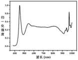
图1是本发明实施例1制备的近红外荧光粉样品的吸收光谱图;FIG1 is an absorption spectrum of a near-infrared phosphor sample prepared in Example 1 of the present invention;
图2是本发明实施例1制备的近红外荧光粉样品的发射光谱图;FIG2 is an emission spectrum of a near-infrared phosphor sample prepared in Example 1 of the present invention;
图3是本发明实施例1制备的近红外荧光粉样品的XRD图;FIG3 is an XRD diagram of a near-infrared phosphor sample prepared in Example 1 of the present invention;
图4(a)为对比例SEM图;图4(b)为实施例59SEM图;Figure 4(a) is a SEM image of a comparative example; Figure 4(b) is a SEM image of Example 59;
图5发光装置的结构图,其中1-发光材料,2-半导体芯片,3-引脚,4-热沉,5-基座,6-玻璃罩;FIG5 is a structural diagram of a light-emitting device, wherein 1 is a light-emitting material, 2 is a semiconductor chip, 3 is a lead, 4 is a heat sink, 5 is a base, and 6 is a glass cover;
图6实施例65提供发光装置的光谱图。FIG6 shows an embodiment 65 that provides a spectrum diagram of a light-emitting device.
具体实施方式DETAILED DESCRIPTION
需要说明的是,在不冲突的情况下,本申请中的实施例及实施例中的特征可以相互组合。下面将结合实施例来详细说明本发明。It should be noted that, in the absence of conflict, the embodiments and features in the embodiments of the present application can be combined with each other. The present invention will be described in detail below in conjunction with the embodiments.
为使本发明的目的、技术方案和优点更加清楚明了,下面结合具体实施方式并参照附图,对本发明进一步详细说明。应该理解,这些描述只是示例性的,而并非要限制本发明的范围。此外,在以下说明中,省略了对公知结构和技术的描述,以避免不必要地混淆本发明的概念。In order to make the purpose, technical scheme and advantages of the present invention clearer, the present invention is further described in detail below in conjunction with specific embodiments and with reference to the accompanying drawings. It should be understood that these descriptions are only exemplary and are not intended to limit the scope of the present invention. In addition, in the following description, the description of well-known structures and technologies is omitted to avoid unnecessary confusion of the concept of the present invention.
如背景技术所记载的,目前近红外荧光粉的研究刚刚起步,材料种类匮乏、光谱覆盖范围较单一、发光效率较低,尤其缺乏发射峰值波长位置位于870-910nm波段发射的高效近红外荧光粉,进而使荧光转换型近红外LED器件应用受到限制,为了解决该问题,本申请提供了一种荧光粉和具有该荧光粉的发光器件。As described in the background technology, the research on near-infrared phosphors is just in its infancy. There is a shortage of material types, a relatively single spectral coverage range, and low luminous efficiency. In particular, there is a lack of high-efficiency near-infrared phosphors with an emission peak wavelength in the 870-910nm band. This has limited the application of fluorescence-converted near-infrared LED devices. In order to solve this problem, the present application provides a phosphor and a light-emitting device having the phosphor.
根据本发明的一个实施例,提供一种近红外荧光粉,所述近红外荧光粉包含组成式A1-d-m-e-x-yDdMmEePfOz:xCr,yG的无机化合物,其中,A元素为Sc、Ga、Al、In中的一种或两种;D元素为La、Gd、Tb中的一种或两种;M元素为Ca、Sr、Ba、Mg、Zn中的一种或两种;E元素为Li、Na、K中的一种或两种;G元素为Pr、Eu、Bi中的一种;其中0<d≤1,0≤m≤0.3,0≤e≤0.2,2.8≤f≤3.2,8.7≤z≤9.5,0<x≤0.5,0≤y≤0.15,所述近红外荧光粉具有立方晶系的ScP3O9晶体结构。以下理论阐述均是在具有荧光粉晶体结构前提下展开的,其中化合物中必含有D元素,D元素为La、Gd、Tb中的一种或两种元素,且D元素进入A元素的格位中。一方面,由于D元素的离子半径远大于A元素的离子,因此,当形成荧光粉的无机化合物中必含有D元素时,会导致原来的配体位膨胀,导致原有晶体场环境减弱,使得具有该无机化合物的荧光粉的发射光谱易于调控,进而得到多个发射波段的近红外荧光粉材料;另一方面,D元素的活泼性均较强,有利于得到增大发光中心辐射跃迁的机率,提升材料发光强度等光学性能。According to one embodiment of the presentinvention , a near- infrared phosphor is provided, comprising an inorganic compound of a composition formulaA1-dmexyDdMmEePfOz :xCr,yG, wherein the A element is one or two of Sc, Ga, Al, and In; the D element is one or two of La, Gd, and Tb; the M element is one or two ofCa , Sr, Ba, Mg, and Zn; the E element is one or two of Li, Na, and K; and the G element is one of Pr, Eu, and Bi; wherein 0<d≤1, 0≤m≤0.3, 0≤e≤0.2, 2.8≤f≤3.2,8.7≤z≤9.5, 0<x≤0.5, and 0≤y≤0.15, and the near-infrared phosphor has a cubicScP3O9crystal structure. The following theoretical explanations are all based on the premise of a phosphor crystal structure, in which the compound must contain D element, which is one or two elements among La, Gd, and Tb, and the D element enters the lattice site of the A element. On the one hand, since the ion radius of the D element is much larger than the ion of the A element, when the inorganic compound that forms the phosphor must contain the D element, it will cause the original ligand site to expand, resulting in the weakening of the original crystal field environment, making the emission spectrum of the phosphor with the inorganic compound easy to control, thereby obtaining near-infrared phosphor materials with multiple emission bands; on the other hand, the activity of the D element is relatively strong, which is conducive to increasing the probability of radiation transition of the luminescent center and improving the optical properties such as the luminescence intensity of the material.
基于上述原理考虑,优选上述近红外荧光粉中D元素为La元素,且0<d≤0.2。在镧系元素中,La3+半径最大,活泼型最强。随着大半径La3+的含量增加,会导致原来的配体位扩张,改变晶体场强度,荧光粉的发射光谱容易发生移动;由于La元素较强的活泼型,发光强度随着La含量的增加,首先出现提升到极值,后随La元素含量的继续增加而降低,降低的主要原因是材料的包容度达到极限值,La元素过量有可能出现杂质,改变目标产物的晶体结构。因此,可以获得不同光学性能的荧光粉,且无机化合物具有与ScP3O9相同的晶体结构。根据实验研究发现,D元素为La元素时,优选0<d≤0.2。Based on the above principle, it is preferred that the D element in the above near-infrared phosphor is La, and 0<d≤0.2. Among the lanthanide elements, La3+ has the largest radius and the strongest active type. As the content of large-radius La3+ increases, the original ligand position will expand, the crystal field strength will change, and the emission spectrum of the phosphor will easily move; due to the strong active type of La element, the luminous intensity will first increase to an extreme value as the La content increases, and then decrease as the La content continues to increase. The main reason for the decrease is that the tolerance of the material reaches the limit value, and an excess of La element may cause impurities to appear, changing the crystal structure of the target product. Therefore, phosphors with different optical properties can be obtained, and the inorganic compound has the same crystal structure as ScP3 O9. According to experimental studies, when the D element is La, 0<d≤0.2 is preferred.
在本申请中另一种优选的实施例中,优选近红外荧光粉中D元素为Gd元素,0<d≤0.3。Gd是镧系元素中常作为基质元素中半径以及活泼性仅次于La的元素。随着较大半径Gd3+含量增加,会导致原来的配体位扩张,改变晶体场强度,荧光粉的发射光谱容易发生移动,可以获得具有不同发射波段、光学性能的荧光粉。另一方面,Gd元素具有较强的活泼型,有利于增大发光中心辐射跃迁的机率,提升材料发光强度等光学性能。而且,Gd3+在基质中具有辐射跃迁(例如:6PJ-8S7/2),能够为发光中心提供除激发光源外的激发能量,有利于提高荧光粉是发光强度。因此,随着Gd元素含量增加,荧光粉发光强度首先出现提升到极值,后随Gd元素含量的继续增加而降低,降低的主要原因是材料的包容度达到极限值,Gd元素过量有可能出现杂质,改变目标产物的晶体结构。根据实验研究,D元素为Gd元素时,优选0<d≤0.3。In another preferred embodiment of the present application, the D element in the near-infrared phosphor is preferably the Gd element, 0<d≤0.3. Gd is an element in the lanthanide series that is often used as a matrix element and is second only to La in radius and activity. As the content of Gd3+ with a larger radius increases, the original ligand position will expand, the crystal field intensity will change, and the emission spectrum of the phosphor will easily move, so that phosphors with different emission bands and optical properties can be obtained. On the other hand, the Gd element has a strong active type, which is conducive to increasing the probability of radiation transition of the luminescent center and improving the optical properties such as the luminescent intensity of the material. Moreover, Gd3+ has a radiation transition in the matrix (for example:6 PJ -8 S7/2 ), which can provide the luminescent center with excitation energy other than the excitation light source, which is conducive to improving the luminescent intensity of the phosphor. Therefore, as the content of the Gd element increases, the luminescent intensity of the phosphor first appears to be increased to an extreme value, and then decreases as the content of the Gd element continues to increase. The main reason for the decrease is that the tolerance of the material reaches the limit value, and the excess of the Gd element may cause impurities to appear, changing the crystal structure of the target product. According to experimental studies, when the D element is the Gd element, 0<d≤0.3 is preferred.
在本申请中另一种优选的实施例中,优选近红外荧光粉中所述A元素为Sc元素和In元素,In占据A元素的摩尔百分比为i,0%<i≤15%。In元素相比于Sc、Ga、Al元素具有更大的离子半径,有利于原来的配体位体积发生扩张,降低晶体场强度,荧光粉的发射光谱容易发生长波移动。另一方面,In3+相比于Sc3+、Ga3+、Al3+具有更高的电负性,容易与O2-形成共价性更强的化学键。共价键越强,电子云扩散效应越强,电子的质心位移更大,进一步使发射光谱向长波移动。同时,较强的共价键性有利于增大发光中心辐射跃迁的机率,提升材料发光强度等光学性能。因此,随着In含量的增加,发射光谱向长波移动。根据实验研究发现,当In含量过少时,发光强度较低,当In元素含量过高时,会产生浓度猝灭、杂质出现、目标产物的晶体结构改变等现象,而造成无辐射跃迁增强,因此发光强度同样较低,因此,In占据A元素的摩尔百分比为i,0%<i≤15%。最终,可以获得不同光学性能的荧光粉,且无机化合物具有与ScP3O9相同的晶体结构。根据实验研究,In占据A元素的摩尔百分比为i,优选0%<i≤15%。In another preferred embodiment of the present application, the A element in the preferred near-infrared phosphor is Sc element and In element, and the molar percentage of In in the A element is i, 0%<i≤15%. Compared with Sc, Ga, and Al elements, the In element has a larger ionic radius, which is conducive to the expansion of the original ligand site volume, reduces the crystal field strength, and the emission spectrum of the phosphor is prone to long-wave shift. On the other hand, In3+ has a higher electronegativity than Sc3+ , Ga3+ , and Al3+ , and is easy to form a stronger covalent chemical bond with O2- . The stronger the covalent bond, the stronger the electron cloud diffusion effect, the greater the displacement of the center of mass of the electron, and further shifts the emission spectrum to the long wave. At the same time, a stronger covalent bond is conducive to increasing the probability of radiation transition of the luminescent center and improving the optical properties such as the luminous intensity of the material. Therefore, as the In content increases, the emission spectrum moves to the long wave. According to experimental research, when the In content is too low, the luminescence intensity is low. When the In content is too high, concentration quenching, impurities appear, and the crystal structure of the target product changes, resulting in non-radiative transition enhancement, so the luminescence intensity is also low. Therefore, the molar percentage of In in the A element is i, 0%<i≤15%. Finally, phosphors with different optical properties can be obtained, and the inorganic compound has the same crystal structure as ScP3 O9. According to experimental research, the molar percentage of In in the A element is i, preferably 0%<i≤15%.
在本申请中另一种优选的实施例中,优选近红外荧光粉中G元素为Pr和Eu中的一种。当G元素为Pr时,0<y≤0.1;当G元素为Eu,0<y≤0.15。基质单独掺杂Cr3+的吸收光谱覆盖蓝光和红光波段。当G元素为Pr、Eu、Bi中的一种时,G元素的离子可以作为敏化剂掺杂进入基质中,其发射光谱与Cr3+吸收光谱重合,能够进行G元素的离子到Cr3+的能量传递,提高Cr3+近红外发光强度。其中,G元素为Pr、Eu时,上述敏化剂掺杂进入基质中表现红光发射,与Cr3+吸收光谱重合度更佳,能量传递效果更佳,近红外发光强度更高。根据实验研究发现,当G元素含量过少时,由于敏化剂少,能量传递效果不明显,发光强度较低,当G元素含量过高时,会发生浓度猝灭而造成无辐射跃迁增强,因此发光强度同样较低,因此,辅助以实验验证,当G元素为Pr时,有优选0.04<y≤0.1;当G元素为Eu,优选0.05<y≤0.15;当G元素为Bi时,有优选0.09<y≤0.15。In another preferred embodiment of the present application, the G element in the near-infrared phosphor is preferably one of Pr and Eu. When the G element is Pr, 0<y≤0.1; when the G element is Eu, 0<y≤0.15. The absorption spectrum of the matrix doped with Cr3+ alone covers the blue and red light bands. When the G element is one of Pr, Eu, and Bi, the ions of the G element can be doped into the matrix as a sensitizer, and its emission spectrum coincides with the absorption spectrum of Cr3+ , which can transfer energy from the ions of the G element to Cr3+ , thereby increasing the near-infrared luminescence intensityof Cr3+ . Among them, when the G element is Pr or Eu, the above-mentioned sensitizer is doped into the matrix to exhibit red light emission, which has a better coincidence with the absorption spectrumof Cr3+ , a better energy transfer effect, and a higher near-infrared luminescence intensity. According to experimental research, when the G element content is too little, due to the small amount of sensitizer, the energy transfer effect is not obvious and the luminescence intensity is low. When the G element content is too high, concentration quenching will occur, resulting in enhanced non-radiative transition, so the luminescence intensity is also low. Therefore, with the assistance of experimental verification, when the G element is Pr, the preferred value is 0.04<y≤0.1; when the G element is Eu, the preferred value is 0.05<y≤0.15; when the G element is Bi, the preferred value is 0.09<y≤0.15.
进一步的,优选M元素为Ca、Sr、Ba中的一种,0<m≤0.12。Ca、Sr、Ba作为碱土金属元素,是化学活泼性较强的金属元素,且活泼性比Mg、Zn更强,有利于增大发光中心辐射跃迁的机率,提升材料发光强度等光学性能;而且,二价的M离子掺杂进入三价的A离子格位,能够在材料中形成例如氧空位等缺陷,适量的缺陷能够帮助进一步提升发光中心辐射跃迁机率,提高发光强度。根据实验研究发现,当M元素含量过少时,由于缺陷浓度小,发光强度较低,当M元素含量过高时,杂质或者过量的缺陷会造成无辐射跃迁增强,因此发光强度同样较低,因此,优选0<m≤0.12。Furthermore, it is preferred that the M element is one of Ca, Sr, and Ba, and 0<m≤0.12. Ca, Sr, and Ba, as alkaline earth metal elements, are metal elements with strong chemical activity, and their activity is stronger than that of Mg and Zn, which is beneficial to increase the probability of radiation transition of the luminescent center and improve the optical properties such as the luminescent intensity of the material; moreover, the divalent M ions are doped into the trivalent A ion lattice, which can form defects such as oxygen vacancies in the material. The right amount of defects can help further improve the probability of radiation transition of the luminescent center and improve the luminescent intensity. According to experimental studies, when the content of the M element is too little, the luminescent intensity is low due to the small defect concentration. When the content of the M element is too high, impurities or excessive defects will cause the non-radiative transition to be enhanced, so the luminescent intensity is also low. Therefore, 0<m≤0.12 is preferred.
进一步的,另一种优选的实施例中,E元素为Li、Na、K,0<e≤0.06。Li、Na、K都是金属,最外层电子数为1,原子核对最外层核外电子的束缚较小,因此原料的熔沸点较低,对荧光粉有助熔效果,有利于提高荧光粉的结晶性能以及单晶颗粒大小,提升发光强度。根据实验研究发现,当E元素含量过少时,由于助熔效果不明显,发光强度较低,当E元素含量过高时,有可能导致杂质产生,因此发光强度同样较低,因此,优选0<e≤0.06。Furthermore, in another preferred embodiment, the E element is Li, Na, K, and 0<e≤0.06. Li, Na, and K are all metals, and the number of outermost electrons is 1. The nucleus has a small bond to the outermost electrons outside the nucleus, so the melting and boiling points of the raw materials are low, which has a fluxing effect on the phosphor, and is beneficial to improve the crystallization performance and single crystal particle size of the phosphor, and enhance the luminous intensity. According to experimental studies, when the content of the E element is too little, the luminous intensity is low due to the insignificant fluxing effect. When the content of the E element is too high, impurities may be generated, so the luminous intensity is also low. Therefore, 0<e≤0.06 is preferred.
进一步的,根据实验研究发现,在E元素为Li的条件下,M元素为Ca、Sr、Ba中的一种,0<e≤0.05,0<m≤3/2e。M元素较少量时,由于三价M离子进入二价A离子格位,电荷不平衡,在荧光粉中形成微量的缺陷,这些缺陷不足以有效提升发光强度,反而导致发光强度较低。在A位置当中掺杂进入与A半径较为相似的Li+,在不改变原A格位大小的条件下,进行电荷补偿以及助熔,提升荧光粉发光强度。从图4所示的SEM图可以发现,加入Li助剂的荧光粉形貌得到大幅提升,不仅呈现类球状,而且形貌更加规则,有利于荧光粉发光强度的提升。除此之外,更加规则的形貌有利于荧光粉的封装,使发光器件具有更加优异的光学性能。Further, according to experimental research, it is found that under the condition that the E element is Li, the M element is one of Ca, Sr, and Ba, 0<e≤0.05, 0<m≤3/2e. When the M element is small in amount, due to the trivalent M ions entering the divalent A ion lattice, the charge is unbalanced, and trace defects are formed in the phosphor. These defects are not enough to effectively improve the luminous intensity, but instead lead to low luminous intensity. Doping Li+ with a radius similar to A into the A position, without changing the original A lattice size, charge compensation and fluxing are performed to improve the luminous intensity of the phosphor. From the SEM image shown in Figure 4, it can be found that the morphology of the phosphor with the addition of Li additives is greatly improved. It not only presents a spherical shape, but also has a more regular morphology, which is conducive to the improvement of the luminous intensity of the phosphor. In addition, a more regular morphology is conducive to the encapsulation of the phosphor, so that the light-emitting device has better optical properties.
O离子为基质中的唯一阴离子,取值范围8.7≤z≤9.5,一方面有利于平衡材料中的正负电荷,防止材料出现严重的电荷失衡,导致发光猝灭;另一方面,氧原子在材料中与其他阳离子元素形成多面体,各个多面体以氧原子作为链接点,形成整个材料的晶胞结构,适当范围的O含量能够保证材料的纯相结构,以此保证材料结构不崩塌,保证材料的性能,否则会导致发光猝灭。O ion is the only anion in the matrix, with a value range of 8.7≤z≤9.5. On the one hand, it is beneficial to balance the positive and negative charges in the material and prevent serious charge imbalance in the material, which leads to luminescence quenching. On the other hand, oxygen atoms form polyhedrons with other cationic elements in the material. Each polyhedron uses oxygen atoms as a link point to form the unit cell structure of the entire material. An appropriate range of O content can ensure the pure phase structure of the material, thereby ensuring that the material structure does not collapse and the performance of the material is guaranteed, otherwise it will lead to luminescence quenching.
P元素作为基质中的重要元素,在取值范围2.8≤f≤3.2内,能够保证材料的纯相结构,以此保证材料结构不崩塌,保证材料的性能,否则会导致发光猝灭。As an important element in the matrix, the P element can ensure the pure phase structure of the material within the value range of 2.8≤f≤3.2, thereby ensuring that the material structure does not collapse and ensuring the performance of the material, otherwise it will lead to luminescence quenching.
Cr元素作为发光中心,即激活剂,能够使材料发生近红外光,根据实验验证,其含量取值范围在0<x≤0.5较优,当Cr元素含量过少时,发光强度较低,当Cr浓度过高时,容易导致发光猝灭。G元素作为敏化剂,其发射光谱与Cr吸收光谱重合,能够进行G元素的离子到Cr的能量传递,提高Cr近红外发光强度,且辅助以实验验证,其含量取值范围在0≤y≤0.15较优,当G元素含量过少时,由于敏化剂少,能量传递效果不明显,发光强度较低,当G元素含量过高时,会发生浓度猝灭而造成无辐射跃迁增强,因此发光强度同样较低。Cr element, as the luminescent center, i.e., activator, can make the material emit near-infrared light. According to experimental verification, its content is preferably in the range of 0<x≤0.5. When the Cr content is too little, the luminescence intensity is low. When the Cr concentration is too high, it is easy to cause luminescence quenching. G element, as a sensitizer, has an emission spectrum that coincides with the Cr absorption spectrum, and can transfer energy from G element ions to Cr, thereby increasing the near-infrared luminescence intensity of Cr. With the aid of experimental verification, its content is preferably in the range of 0≤y≤0.15. When the G content is too little, due to the small amount of sensitizer, the energy transfer effect is not obvious, and the luminescence intensity is low. When the G content is too high, concentration quenching occurs, resulting in non-radiative transition enhancement, so the luminescence intensity is also low.
本发明上述的荧光粉可以优选采用本申请所提供的以下制备方法,该制备方法包括:步骤1),以选自A元素、D元素、M元素、E元素、P元素、Cr元素和G元素的单质、氮化物、氧化物或它们的合金为原料,将原料混合得到混合体;步骤2),将步骤1)得到的混合体放入容器并在氮气或其他非氧化气氛下焙烧,得到焙烧产物,其中,最高烧结温度为1000~1500℃,保温时间为3~15h;步骤3),将步骤2中的焙烧产物依次破碎、洗涤、过筛和烘干后处理得到荧光粉。The above-mentioned phosphor of the present invention can preferably adopt the following preparation method provided in the present application, which comprises: step 1), using a single substance, nitride, oxide or alloy thereof selected from element A, element D, element M, element E, element P, element Cr and element G as raw materials, mixing the raw materials to obtain a mixture; step 2), placing the mixture obtained in step 1) into a container and calcining it under nitrogen or other non-oxidizing atmosphere to obtain a calcined product, wherein the maximum sintering temperature is 1000-1500°C and the insulation time is 3-15h; step 3), crushing, washing, sieving and drying the calcined product in step 2 in sequence to obtain a phosphor.
具有上述组成的无机化合物的荧光粉激发光谱峰值波长位于420~480nm,且发射峰值波长覆盖870-910nm的区间。The peak wavelength of the excitation spectrum of the phosphor of the inorganic compound with the above composition is located at 420-480nm, and the peak wavelength of the emission covers the range of 870-910nm.
在本申请另一种典型的实施方式中,提供了一种发光器件,包括荧光体和激发光源,该荧光体包括上述的荧光粉。由于本申请的荧光粉具有热稳定性高、发射光谱易于调控,因此,使得具有其的发光器件的工作稳定性高、使用寿命较长,且适用于多种不同需求。In another typical embodiment of the present application, a light-emitting device is provided, including a phosphor and an excitation light source, wherein the phosphor includes the above-mentioned phosphor. Since the phosphor of the present application has high thermal stability and an emission spectrum that is easy to control, the light-emitting device having the phosphor has high working stability, a long service life, and is applicable to a variety of different needs.
在一种优选的实施例中,上述激发光源为半导体发光二极管光源,进一步优选激发光源的发射峰值波长为420-480nm的半导体芯片。目前商用LED激发光源其激发波段在此范围内,具体有两种激发光源,利用上述波长范围内的发光二极管有利于荧光粉的光致发光。In a preferred embodiment, the excitation light source is a semiconductor light emitting diode light source, and further preferably, the excitation light source has a semiconductor chip with an emission peak wavelength of 420-480nm. Currently, the excitation wavelength band of commercial LED excitation light sources is within this range, and there are two specific excitation light sources. The use of light emitting diodes within the above wavelength range is conducive to the photoluminescence of the phosphor.
为了进一步改善发光器件的发光效果,优选上述荧光体还包括其他荧光粉,包含发射波长范围为500-780nm的可见光荧光粉以及发射波长范围为950-1100nm的近红外荧光粉。所述可见光荧光粉为发射波长范围在500-780nm的荧光粉,包括但不局限于(Ca,Sr,Ba)5(PO4)3(Cl,Br,F):Eu2+、(Mg,Zn)(Ca,Sr,Ba)3Si2O8:Eu2+、(Ca,Sr,Ba)Si2N2O2:Eu2+、β-SiAlON:Eu2+、(Lu,Y,Gd)3(Al,Ga)5O12:Ce3+,Tb3+、(Lu,Y,Gd)3(Al,Ga)5O12:Ce3+、(La,Y,Lu)3Si6N11:Ce3+、(Ca,Sr,Ba)2Si5N8:Eu2+、(Ca,Sr)AlSiN3:Eu2+、K2(Si,Ge)F6:Mn4+、(Sr,Ca,Ba)4(Al,Sc,Ga,In)14O25:Mn4+、(La,Y,Gd,Lu)3(Al,Ga)(Ge,Si)5O16:Mn4+、(Lu,Y,Gd)3(Al,Ga)5O12:Mn4+中的一种或者多种。所述近红外荧光粉为发射波长范围在950-1100nm的荧光粉,包括但不局限于(La,Y,Gd,Lu)3(Al,Ga)5(Ge,Si)O14:Cr3+,Yb3+、Sc2O3·Ga2O3·(Cr,Yb,Nd,Er)2O3、(La,Lu,Y,Gd)(Sc,Ga,Al,In)3B4O12:Cr3+,Yb3+中的一种或者多种。其中,各物质中“,”表示圆括号内元素可为单一组分或含一种元素以上的固溶体,例如:(Ca,Sr)AlSiN3:Eu2+表示为CaAlSiN3:Eu2+、SrAlSiN3:Eu2+和Ca1-αSrαAlSiN3:Eu2+(0<α<1)中的一种或者几种的固溶体。将本发明的近红外荧光粉与上述荧光粉进行配合使用,使得发光器件发出高光效、光谱连续性优异的光,以满足包含环境光源、全光谱健康照明、医食检测、水质检测等领域在内的众多传统以及新型领域的应用需要。In order to further improve the luminous effect of the light-emitting device, the phosphor preferably further includes other phosphors, including visible light phosphors with an emission wavelength range of 500-780 nm and near-infrared phosphors with an emission wavelength range of 950-1100 nm. The visible light phosphor is a phosphor with an emission wavelength range of 500-780 nm, including but not limited to (Ca, Sr, Ba)5 (PO4 )3 (Cl, Br, F):Eu2+ , (Mg, Zn)(Ca, Sr, Ba)3 Si2 O8 :Eu2+ , (Ca, Sr, Ba) Si2 N2 O2 :Eu2+ , β-SiAlON:Eu2+ , (Lu, Y, Gd)3 (Al, Ga)5 O12 :Ce3+ , Tb3+ , (Lu, Y, Gd)3 (Al, Ga)5 O12 :Ce3+ , (La, Y, Lu)3 Si6 N11 :Ce3+ , (Ca, Sr, Ba)2 Si5 N8 :Eu2+ , (Ca,Sr)AlSiN3 :Eu2+ , K2 (Si,Ge)F6 :Mn4+ , (Sr,Ca,Ba)4 (Al,Sc,Ga,In)14 O25 :Mn4+ , (La,Y,Gd,Lu)3 (Al,Ga)(Ge,Si)5 O16 :Mn4+ , and (Lu,Y,Gd)3 (Al,Ga)5 O12 :Mn4+ . The near-infrared phosphor is a phosphor with an emission wavelength range of 950-1100 nm, including but not limited to one or more of (La, Y, Gd, Lu)3 (Al, Ga)5 (Ge, Si)O14 :Cr3+ , Yb3+ , Sc2 O3 ·Ga2 O3 ·(Cr, Yb, Nd, Er)2 O3 , and (La, Lu, Y, Gd)(Sc, Ga, Al, In)3 B4 O12 :Cr3+ , Yb3+ . Among them, "," in each substance means that the element in the parentheses can be a single component or a solid solution containing more than one element, for example: (Ca, Sr) AlSiN3 :Eu2+ is represented by one or more solid solutions of CaAlSiN3 :Eu2+ , SrAlSiN3 :Eu2+ and Ca1-α Srα AlSiN3 :Eu2+ (0<α<1). The near-infrared phosphor of the present invention is used in combination with the above-mentioned phosphors, so that the light-emitting device emits light with high light efficiency and excellent spectral continuity, so as to meet the application needs of many traditional and new fields including ambient light sources, full-spectrum health lighting, medical and food testing, water quality testing and other fields.
以下为本发明的具体实施例,只是为了说明本发明所涉及的近红外荧光粉以及光学装置,但本发明并不局限于下述各实施例。The following are specific embodiments of the present invention, which are only for illustrating the near-infrared phosphor and the optical device involved in the present invention, but the present invention is not limited to the following embodiments.
实施例1Example 1
本实施例所提供的近红外荧光粉,其包含的化合物组成式为Sc0.8Tb0.1P3O9:0.10Cr。按照化学式的化学计量比,并对称取的氧化物原料进行研磨混合,得到混合体;将所述混合体经研磨及混匀后于1280℃煅烧5h,降温后获得焙烧产物;将所得焙烧产物进行破碎、研磨、分级、筛洗等后处理,即可得到近红外荧光粉中间体。The near-infrared phosphor provided in this embodiment has a compound composition formula of Sc0.8 Tb0.1 P3 O9 :0.10Cr. According to the stoichiometric ratio of the chemical formula, the oxide raw materials are ground and mixed to obtain a mixture; the mixture is ground and mixed, and then calcined at 1280° C. for 5 hours, and a calcined product is obtained after cooling; the calcined product is post-processed by crushing, grinding, grading, screening and washing to obtain a near-infrared phosphor intermediate.
利用荧光光谱仪对所得近红外样品进行激发、发射光谱测试,通过该实施例1制备的近红外荧光粉样品的吸收、发射光谱图如图1-2所示。从图1-2可以看出,所得近红外荧光粉样品在410-500nm,600-780nm范围内均具有有效吸收,且发射波长覆盖800-1050nm,发射峰位置位于881nm。所得结果列于表1中。The obtained near-infrared sample was tested for excitation and emission spectra using a fluorescence spectrometer, and the absorption and emission spectra of the near-infrared phosphor sample prepared by this Example 1 are shown in Figures 1-2. As can be seen from Figures 1-2, the obtained near-infrared phosphor sample has effective absorption in the range of 410-500nm and 600-780nm, and the emission wavelength covers 800-1050nm, and the emission peak position is located at 881nm. The obtained results are listed in Table 1.
表1Table 1


上述实施例1-67以及对比例制得近红外荧光粉的材料、发光性能表征结果如表1所示。注:以对比例的发光强度为基准值100计,实施例的相对发光强度为其实际发光强度除以对比例的实际发光强度,再乘以100%。The materials and luminescence performance characterization results of the near-infrared phosphors prepared in the above Examples 1-67 and Comparative Examples are shown in Table 1. Note: Taking the luminescence intensity of the comparative example as the reference value 100, the relative luminescence intensity of the embodiment is its actual luminescence intensity divided by the actual luminescence intensity of the comparative example, multiplied by 100%.
通过上述表1中实施例对比例各项数据之间的对比,不难发现:对于具有A1-d-m-e-x-yDdMmEePfOz:xCr,yG中采用较大的稀土元素La、Gd、Tb适量取代A元素;A元素同时有Sc、In;选取适当的在红光区域具有发射的敏化剂;采用较大半径的非等价碱土金属适量取代A元素,并加入既可以当作电荷补偿剂又可以作为助溶剂的一价元素;上述方式均能够实现光谱发射峰值位置在870-910nm波段范围的调控以及发光强度提升,得到更高效的近红外发射。By comparing the data of the comparativeexamples in the above Table 1, it is not difficult to find that: for A1-dmex-yDdMmEePfOz:xCr, yG, larger rare earth elements La, Gd, Tb are used to replace the A element in an appropriate amount; the A element also includes Sc and In; an appropriate sensitizer with emission in the red light region is selected; a non-equivalent alkaline earth metal with a larger radius is used to replace the A element in an appropriate amount, and a monovalent element that can be used as both a charge compensator and a co-solvent is added; the above methods can achieve the regulation of the spectral emission peak position in the 870-910nm band range and the improvement of the luminous intensity, thereby obtaining more efficient near-infrared emission.
实施例11-14与实施例1对比,发现采用D元素为较大的稀土元素La、Gd适量取代A元素,有利于进行发光强度提升以及发射峰值位置移动。在镧系元素中,La3+半径最大,活泼型最强。随着大半径La3+的含量增加,会导致原来的配体位扩张,改变晶体场强度,荧光粉的发射光谱容易发生移动;由于La元素较强的活泼型,发光强度随着La含量的增加,首先出现提升到极值,后随La元素含量的继续增加而降低,降低的主要原因是材料的包容度达到极限值,La元素过量有可能出现杂质,改变目标产物的晶体结构,因此D元素为La元素时,优选0<d≤0.2。Gd是镧系元素中常作为基质元素中半径以及活泼性仅次于La的元素。随着较大半径Gd3+含量增加,会导致原来的配体位扩张,改变晶体场强度,荧光粉的发射光谱容易发生移动,可以获得具有不同发射波段、光学性能的荧光粉。另一方面,Gd元素具有较强的活泼型,有利于增大发光中心辐射跃迁的机率,提升材料发光强度等光学性能。而且,Gd3+在基质中具有辐射跃迁(例如:6PJ-8S7/2),能够为发光中心提供除激发光源外的激发能量,有利于提高荧光粉是发光强度。因此,随着Gd元素含量增加,荧光粉发光强度首先出现提升到极值,后随Gd元素含量的继续增加而降低,降低的主要原因是材料的包容度达到极限值,Gd元素过量有可能出现杂质,改变目标产物的晶体结构。因此,D元素为Gd元素时,优选0<d≤0.3。Compared with Example 1, Examples 11-14 show that using D elements as larger rare earth elements La and Gd to replace A elements in appropriate amounts is beneficial to improving the luminous intensity and moving the emission peak position. Among the lanthanide elements, La3+ has the largest radius and the strongest activity. As the content of large-radius La3+ increases, the original ligand position will expand, the crystal field strength will change, and the emission spectrum of the phosphor will easily move; due to the strong activity of the La element, the luminous intensity will first increase to an extreme value as the La content increases, and then decrease as the La content continues to increase. The main reason for the decrease is that the tolerance of the material reaches the limit value, and an excess of La may cause impurities to appear, changing the crystal structure of the target product. Therefore, when the D element is La, 0<d≤0.2 is preferred. Gd is an element in the lanthanide element that is often used as a matrix element and is second only to La in radius and activity. As the content of larger-radius Gd3+ increases, the original ligand position will expand, the crystal field strength will change, and the emission spectrum of the phosphor will easily move, and phosphors with different emission bands and optical properties can be obtained. On the other hand, the Gd element has a strong active type, which is conducive to increasing the probabilityof radiation transition of the luminescent center and improving the optical properties such as the luminescent intensity of the material. Moreover, Gd3+ has a radiation transition in the matrix (for example:6PJ -8S7/2 ), which can provide the luminescent center with excitation energy other than the excitation light source, which is conducive to improving the luminescent intensity of the phosphor. Therefore, as the content of the Gd element increases, the luminescent intensity of the phosphor first increases to an extreme value, and then decreases as the content of the Gd element continues to increase. The main reason for the decrease is that the tolerance of the material reaches the limit value, and the excess of the Gd element may cause impurities to appear, changing the crystal structure of the target product. Therefore, when the D element is the Gd element, it is preferred that 0<d≤0.3.
实施例16-17与实施例1对比,发现A元素同时有Sc、In且In占据A元素的摩尔百分比为i,0%<i≤15%有利于发光强度提升以及光谱调控。In元素相比于Sc元素具有更大的离子半径,有利于原来的配体位体积发生扩张,降低晶体场强度,荧光粉的发射光谱容易发生长波移动。另一方面,In3+相比Sc3+具有更高的电负性,容易与O2-形成共价性更强的化学键。共价键越强,电子云扩散效应越强,电子的质心位移更大,进一步使发射光谱向长波移动。同时,较强的共价键性有利于增大发光中心辐射跃迁的机率,提升材料发光强度等光学性能。因此,随着In含量的增加,发射光谱向长波移动。根据实验研究发现,当In含量过少时,发光强度较低,当In元素含量过高时,会产生浓度猝灭、杂质出现、目标产物的晶体结构改变等现象,而造成无辐射跃迁增强,因此发光强度同样较低,因此,In占据A元素的摩尔百分比为i,0%<i≤15%。Compared with Example 1, Examples 16-17 show that the A element contains Sc and In at the same time and the molar percentage of In in the A element is i, and 0%<i≤15% is beneficial to the improvement of luminescence intensity and spectrum regulation. Compared with the Sc element, the In element has a larger ionic radius, which is beneficial to the expansion of the original ligand site volume, reduces the crystal field strength, and the emission spectrum of the phosphor is prone to long-wave shift. On the other hand, In3+ has a higher electronegativity than Sc3+ , and is easy to form a more covalent chemical bond with O2- . The stronger the covalent bond, the stronger the electron cloud diffusion effect, the greater the displacement of the center of mass of the electron, and further shifts the emission spectrum to the long wave. At the same time, stronger covalent bonding is beneficial to increase the probability of radiation transition of the luminescence center and improve the optical properties such as the luminescence intensity of the material. Therefore, as the In content increases, the emission spectrum shifts to the long wave. According to experimental research, when the In content is too little, the luminescence intensity is low. When the In content is too high, concentration quenching, impurities appear, and the crystal structure of the target product changes, which will cause the non-radiative transition to be enhanced, so the luminescence intensity is also low. Therefore, the molar percentage of In in the A element is i, 0%<i≤15%.
实施例23-25与实施例1对比,发现G元素选取适当的在红光区域具有发射的敏化剂Pr、Eu有利于发光强度提升。上述敏化剂G元素掺杂进入基质中表现红光发射,与Cr3+吸收光谱重合度更佳,能量传递效果更佳,近红外发光强度更高。根据实验研究发现,当G元素含量过少时,由于敏化剂少,能量传递效果不明显,发光强度较低,当G元素含量过高时,会发生浓度猝灭而造成无辐射跃迁增强,因此发光强度同样较低。当G元素为Pr时,有优选0<y≤0.1;当G元素为Eu,优选0<y≤0.15。Compared with Example 1, Examples 23-25 show that the selection of appropriate sensitizers Pr and Eu with emission in the red light region for the G element is beneficial to the improvement of the luminous intensity. The above-mentioned sensitizer G element is doped into the matrix to exhibit red light emission, with a better coincidence with the Cr3+ absorption spectrum, a better energy transfer effect, and a higher near-infrared luminous intensity. According to experimental studies, when the G element content is too little, the energy transfer effect is not obvious due to the small amount of sensitizer, and the luminous intensity is low. When the G element content is too high, concentration quenching will occur, resulting in enhanced non-radiative transitions, so the luminous intensity is also low. When the G element is Pr, it is preferably 0<y≤0.1; when the G element is Eu, it is preferably 0<y≤0.15.
实施例59-64相比于实施例11-14、16-17、23-25相比,M元素采用较大半径的二价离子Ca、Sr、Ba适量取代A元素,并加入既可以当作电荷补偿剂又可以作为助熔剂的E元素为一价离子Li、Na、K,有利于得到更高效的近红外发射。优选M元素为Ca、Sr、Ba中的一种,0<m≤0.12。Ca、Sr、Ba作为碱土金属元素,是化学活泼性较强的金属元素,且活泼性比Mg、Zn更强,有利于增大发光中心辐射跃迁的机率,提升材料发光强度等光学性能;而且,二价的M离子掺杂进入三价的A离子格位,能够在材料中形成例如氧空位等缺陷,适量的缺陷能够帮助进一步提升发光中心辐射跃迁机率,提高发光强度。进一步地,根据实验研究发现,M元素较少量时,由于三价M离子进入二价A离子格位,电荷不平衡,在荧光粉中形成微量的缺陷,这些缺陷不足以有效提升发光强度,反而导致发光强度较低。因此,采用E元素为Li、Na、K取代A元素。Li、Na、K都是金属,最外层电子数为1,原子核对最外层核外电子的束缚较小,因此原料的熔沸点较低,对荧光粉有助熔效果,有利于提高荧光粉的结晶性能以及单晶颗粒大小,提升发光强度。根据实验发现,在A位置当中掺杂进入与A半径较为相似的E元素为Li,在不改变原A格位大小的条件下,进行电荷补偿以及助熔,提升荧光粉发光强度。因此,根据实验研究发现,在E元素为Li的条件下,M元素为Ca、Sr、Ba中的一种,0<e≤0.05,0<m≤3/2e。从图4所示的SEM图可以发现,加入Li助剂的荧光粉形貌得到大幅提升,不仅呈现类球状,而且形貌更加规则,有利于荧光粉发光强度的提升。除此之外,更加规则的形貌有利于荧光粉的封装,使发光器件具有更加优异的光学性能。Compared with Examples 11-14, 16-17, and 23-25, in Examples 59-64, the M element uses divalent ions Ca, Sr, and Ba with larger radii to replace the A element in appropriate amounts, and adds E elements that can be used as both charge compensators and fluxes as monovalent ions Li, Na, and K, which is beneficial for obtaining more efficient near-infrared emission. Preferably, the M element is one of Ca, Sr, and Ba, and 0<m≤0.12. Ca, Sr, and Ba, as alkaline earth metal elements, are metal elements with strong chemical activity, and their activity is stronger than that of Mg and Zn, which is beneficial for increasing the probability of radiation transition of the luminescent center and improving the optical properties such as the luminescent intensity of the material; moreover, the divalent M ions are doped into the trivalent A ion lattice, which can form defects such as oxygen vacancies in the material, and the appropriate amount of defects can help further improve the probability of radiation transition of the luminescent center and improve the luminescent intensity. Furthermore, according to experimental research, when the amount of M element is small, the trivalent M ions enter the divalent A ion lattice, the charge is unbalanced, and a trace amount of defects are formed in the phosphor. These defects are not enough to effectively improve the luminous intensity, but instead lead to a low luminous intensity. Therefore, the E element is Li, Na, or K to replace the A element. Li, Na, and K are all metals, with 1 outermost electron number, and the nucleus has a small bond to the outermost extranuclear electrons. Therefore, the melting and boiling points of the raw materials are low, which has a fluxing effect on the phosphor, which is beneficial to improve the crystallization performance and single crystal particle size of the phosphor and improve the luminous intensity. According to experimental findings, the E element doped into the A position with a radius similar to that of A is Li. Under the condition of not changing the size of the original A lattice, charge compensation and fluxing are performed to improve the luminous intensity of the phosphor. Therefore, according to experimental research, under the condition that the E element is Li, the M element is one of Ca, Sr, and Ba, 0<e≤0.05, 0<m≤3/2e. From the SEM image shown in Figure 4, it can be found that the morphology of the phosphor with the addition of Li additive is greatly improved. It is not only spherical, but also more regular in shape, which is conducive to the improvement of the luminous intensity of the phosphor. In addition, the more regular morphology is conducive to the encapsulation of the phosphor, so that the light-emitting device has better optical properties.
下述实施例为以本发明的近红外荧光粉为发光材料制得的发光装置,以现有技术中已知的发光装置结构为例,在某些实施例中,如图4所示,所述发光装置包括发光材料1,半导体芯片2,引脚3,热沉4,基座5,以及玻璃罩6。其中,热沉4固定在基座5上,半导体芯片2固定在热沉4上,引出引脚3,发光材料1覆盖在半导体芯片2上,可见光发光材料层6覆盖在近红外发光材料层1上,玻璃罩6罩在发光材料1外部。The following embodiments are light-emitting devices made with the near-infrared phosphor of the present invention as the light-emitting material. Taking the structure of the light-emitting device known in the prior art as an example, in some embodiments, as shown in FIG4 , the light-emitting device includes a light-emitting
实施例68Embodiment 68
本实施例所述的发光装置以波长为460nm的半导体芯片为光源,发光材料为近红外荧光粉,该近红外荧光粉的化学式为Sc0.64La0.1Ba0.04Na0.04P3O8.94:0.1Cr,0.08Pr,根据化学计量比,准确称取原料,并对称取的原料进行研磨混合,得到混合体;将所述混合体于800℃预烧2h,再在1200℃煅烧5h,降温后获得焙烧产物;将所得焙烧产物进行破碎、研磨、分级、筛洗后处理,得到近红外荧光粉。另外,本实施例中选取发射波长范围在500-780nm的Lu2.94(Al0.8Ga0.2)5O12:0.06Ce3+、(Ca0.9Sr0.1)0.95AlSiN3:0.05Eu2+、(Ca0.15Sr0.85)0.95AlSiN3:0.05Eu2+以及发射波长范围在950-1100nm的近红外荧光粉(La,Y,Gd,Lu)3(Al,Ga)5(Ge,Si)O14:Cr3+,Yb3+、Sc2O3·Ga2O3·Cr2O3。将本实施例中荧光粉与硅胶按照质量比1:1混合均匀,搅拌、脱泡,得到荧光转换层混合料,将该混合料通过喷涂的方式覆盖在LED芯片层表面,通过烘烤使其固化成可见光荧光层,封装后获得所需的LED发光装置。采用高精度快速光谱辐射计积分球测试系统,用恒定电流点亮各实施例提供的光学装置的光源(正向电压3.234V,正向电流350.0mA),测试得到本实施例所述发光装置的光功率为151.00mW,光谱图如图6。The light-emitting device described in this embodiment uses a semiconductor chip with a wavelength of 460nm as a light source, and the light-emitting material is a near-infrared phosphor. The chemical formula of the near-infrared phosphor is Sc0.64 La0.1 Ba0.04 Na0.04 P3 O8.94 :0.1Cr, 0.08Pr. According to the stoichiometric ratio, the raw materials are accurately weighed, and the symmetrically taken raw materials are ground and mixed to obtain a mixture; the mixture is pre-calcined at 800°C for 2h, and then calcined at 1200°C for 5h, and a calcined product is obtained after cooling; the obtained calcined product is crushed, ground, classified, screened and washed, and then processed to obtain the near-infrared phosphor. In addition, in this embodiment, Lu2.94 (Al0.8 Ga0.2 )5 O12 :0.06Ce3+ , (Ca0.9 Sr0.1 )0.95 AlSiN3 :0.05Eu2+ , (Ca0.15 Sr0.85 )0.95 AlSiN 3 :0.05Eu2+ , and near-infrared phosphors (La, Y, Gd, Lu)3 (Al, Ga)5 (Ge, Si)O14 :Cr3+ , Yb3+ , and Sc2 O3 ·Ga2 O3 ·Cr2 O3 , with anemission wavelength range of 500-780 nm, are selected. The phosphor and silica gel in this embodiment are mixed evenly in a mass ratio of 1:1, stirred and degassed to obtain a fluorescent conversion layer mixture, which is sprayed on the surface of the LED chip layer, cured into a visible light fluorescent layer by baking, and packaged to obtain the desired LED light-emitting device. A high-precision fast spectroradiometer integrating sphere test system is used to light the light source of the optical device provided in each embodiment with a constant current (forward voltage 3.234V, forward current 350.0mA), and the light power of the light-emitting device in this embodiment is tested to be 151.00mW, and the spectrum is shown in Figure 6.
本发明各实施例近红外发光材料封装得到的光学装置的性能参数如表2所示。The performance parameters of the optical device encapsulated by the near-infrared luminescent material of each embodiment of the present invention are shown in Table 2.
表2Table 2

从以上表2可以看出从上表数据可看出,本发明所述光学装置中的荧光粉可以有效被LED芯片激发,并通过复合可见光发光材料、近红外发光材料的光学装置,能实现500-780nm波段可见光和780-1100nm波段近红外的双重发射,且器件光通量适宜,在环境光源、水质检测、医食检测、全光谱健康照明等领域具有巨大应用前景。It can be seen from the data in Table 2 above that the phosphor in the optical device of the present invention can be effectively excited by the LED chip, and the optical device of the composite visible light luminescent material and the near-infrared luminescent material can achieve dual emission of visible light in the 500-780nm band and near-infrared in the 780-1100nm band, and the device has an appropriate luminous flux, and has great application prospects in the fields of ambient light sources, water quality testing, medical and food testing, full-spectrum health lighting, etc.
应当理解的是,本发明的上述具体实施方式仅仅用于示例性说明或解释本发明的原理,而不构成对本发明的限制。因此,在不偏离本发明的精神和范围的情况下所做的任何修改、等同替换、改进等,均应包含在本发明的保护范围之内。此外,本发明所附权利要求旨在涵盖落入所附权利要求范围和边界、或者这种范围和边界的等同形式内的全部变化和修改例。It should be understood that the above specific embodiments of the present invention are only used to illustrate or explain the principles of the present invention, and do not constitute a limitation of the present invention. Therefore, any modifications, equivalent substitutions, improvements, etc. made without departing from the spirit and scope of the present invention should be included in the protection scope of the present invention. In addition, the appended claims of the present invention are intended to cover all changes and modifications that fall within the scope and boundaries of the appended claims, or the equivalent forms of such scope and boundaries.
Claims (9)
Priority Applications (1)
| Application Number | Priority Date | Filing Date | Title |
|---|---|---|---|
| CN202111539257.0ACN114410302B (en) | 2021-12-15 | 2021-12-15 | Near infrared fluorescent powder and optical device thereof |
Applications Claiming Priority (1)
| Application Number | Priority Date | Filing Date | Title |
|---|---|---|---|
| CN202111539257.0ACN114410302B (en) | 2021-12-15 | 2021-12-15 | Near infrared fluorescent powder and optical device thereof |
Publications (2)
| Publication Number | Publication Date |
|---|---|
| CN114410302A CN114410302A (en) | 2022-04-29 |
| CN114410302Btrue CN114410302B (en) | 2023-05-05 |
Family
ID=81267783
Family Applications (1)
| Application Number | Title | Priority Date | Filing Date |
|---|---|---|---|
| CN202111539257.0AActiveCN114410302B (en) | 2021-12-15 | 2021-12-15 | Near infrared fluorescent powder and optical device thereof |
Country Status (1)
| Country | Link |
|---|---|
| CN (1) | CN114410302B (en) |
Families Citing this family (2)
| Publication number | Priority date | Publication date | Assignee | Title |
|---|---|---|---|---|
| CN116639975B (en)* | 2023-02-24 | 2025-02-18 | 河南工业大学 | Blue light excited wide half-width near-infrared fluorescent ceramics and preparation method and application thereof |
| CN116751588B (en)* | 2023-06-28 | 2024-05-14 | 江西理工大学 | A near-infrared luminescent material, a preparation method thereof and an LED light source containing the material |
Family Cites Families (2)
| Publication number | Priority date | Publication date | Assignee | Title |
|---|---|---|---|---|
| WO2020207773A1 (en)* | 2019-04-12 | 2020-10-15 | Lumileds Holding B.V. | Novel nir broadband emitting phosphors for infrared spectroscopy |
| CN112300797B (en)* | 2020-10-09 | 2022-02-08 | 北京科技大学 | Cr (chromium)3+Doped strontium indium phosphate broadband near-infrared luminescent material and preparation method thereof |
- 2021
- 2021-12-15CNCN202111539257.0Apatent/CN114410302B/enactiveActive
Also Published As
| Publication number | Publication date |
|---|---|
| CN114410302A (en) | 2022-04-29 |
Similar Documents
| Publication | Publication Date | Title |
|---|---|---|
| JP5331981B2 (en) | Silicate-based luminescent material with multiple emission peaks, method for preparing the luminescent material, and light emitting device using the luminescent material | |
| CN104357051B (en) | A kind of fluorescent material and preparation method thereof, and light-emitting device | |
| CN112011332B (en) | Far-red fluorescent powder and light-emitting device comprising same | |
| CN105778913B (en) | A kind of list matrix three adulterates white light phosphor and preparation method and application | |
| CN104818021B (en) | A kind of single-substrate white fluorescent powder of near ultraviolet excitation and preparation method thereof | |
| CN114410302B (en) | Near infrared fluorescent powder and optical device thereof | |
| CN113444521B (en) | Red fluorescent powder and light-emitting device with same | |
| CN114395394B (en) | Near-infrared fluorescent powder and optical device comprising same | |
| CN111187622B (en) | Single matrix phosphate fluorescent powder for white light LED and preparation method thereof | |
| CN105985772B (en) | Fluorescent material for solid light source, method for producing same, and composition containing same | |
| CN114540015A (en) | Wide-spectrum yellow-green emitting nitrogen oxide fluorescent powder and preparation method thereof | |
| CN105131953A (en) | Rare earth ion doping novel polysilicate green fluorescent powder for near ultraviolet stimulated white light LED and preparation method of novel polysilicate green fluorescent powder | |
| CN103320131B (en) | A kind of phosphate-based red fluorescent powder, preparation method and application | |
| CN104087299B (en) | A kind of blue light activated aluminate-based red fluorescent material and preparation method and application | |
| CN117736734A (en) | A blue fluorescent material excited by violet light and its preparation method and application | |
| CN102936497B (en) | Main emission peak changeable and adjustable fluorescent material and preparation method thereof | |
| CN106634996A (en) | Fluorophor and application method thereof | |
| CN115873595A (en) | A kind of controllable red light and near-infrared rare earth luminescent material and its preparation method and infrared LED device | |
| CN115261016A (en) | Blue-violet light-emitting material and preparation method thereof, white light LED | |
| CN106811195A (en) | A kind of novel silicon phosphate compounds luminescent material | |
| CN107916106A (en) | Nitride phosphor and preparation method thereof and the luminescent device for including it | |
| CN112054107A (en) | Optical device and application thereof | |
| CN101619214B (en) | Scheelite mineral phase red fluorescent powder and preparation method thereof | |
| CN105154082A (en) | Rare earth ion-doped vanadium tungstate red phosphor capable of being excited by near ultraviolet and blue ray simultaneously and preparation method of red phosphor | |
| CN115612493B (en) | A UV-excited Eu(Ⅱ) single-doped red light-emitting phosphor and its preparation method and application |
Legal Events
| Date | Code | Title | Description |
|---|---|---|---|
| PB01 | Publication | ||
| PB01 | Publication | ||
| SE01 | Entry into force of request for substantive examination | ||
| SE01 | Entry into force of request for substantive examination | ||
| GR01 | Patent grant | ||
| GR01 | Patent grant |