CN114388596A - Display substrate, preparation method thereof and display device - Google Patents
Display substrate, preparation method thereof and display deviceDownload PDFInfo
- Publication number
- CN114388596A CN114388596ACN202111407120.XACN202111407120ACN114388596ACN 114388596 ACN114388596 ACN 114388596ACN 202111407120 ACN202111407120 ACN 202111407120ACN 114388596 ACN114388596 ACN 114388596A
- Authority
- CN
- China
- Prior art keywords
- conductive layer
- transistor
- electrode
- sub
- display substrate
- Prior art date
- Legal status (The legal status is an assumption and is not a legal conclusion. Google has not performed a legal analysis and makes no representation as to the accuracy of the status listed.)
- Pending
Links
Images


Classifications
- G—PHYSICS
- G09—EDUCATION; CRYPTOGRAPHY; DISPLAY; ADVERTISING; SEALS
- G09G—ARRANGEMENTS OR CIRCUITS FOR CONTROL OF INDICATING DEVICES USING STATIC MEANS TO PRESENT VARIABLE INFORMATION
- G09G3/00—Control arrangements or circuits, of interest only in connection with visual indicators other than cathode-ray tubes
- G09G3/20—Control arrangements or circuits, of interest only in connection with visual indicators other than cathode-ray tubes for presentation of an assembly of a number of characters, e.g. a page, by composing the assembly by combination of individual elements arranged in a matrix no fixed position being assigned to or needed to be assigned to the individual characters or partial characters
- G09G3/22—Control arrangements or circuits, of interest only in connection with visual indicators other than cathode-ray tubes for presentation of an assembly of a number of characters, e.g. a page, by composing the assembly by combination of individual elements arranged in a matrix no fixed position being assigned to or needed to be assigned to the individual characters or partial characters using controlled light sources
- G09G3/30—Control arrangements or circuits, of interest only in connection with visual indicators other than cathode-ray tubes for presentation of an assembly of a number of characters, e.g. a page, by composing the assembly by combination of individual elements arranged in a matrix no fixed position being assigned to or needed to be assigned to the individual characters or partial characters using controlled light sources using electroluminescent panels
- G09G3/32—Control arrangements or circuits, of interest only in connection with visual indicators other than cathode-ray tubes for presentation of an assembly of a number of characters, e.g. a page, by composing the assembly by combination of individual elements arranged in a matrix no fixed position being assigned to or needed to be assigned to the individual characters or partial characters using controlled light sources using electroluminescent panels semiconductive, e.g. using light-emitting diodes [LED]
- G09G3/3208—Control arrangements or circuits, of interest only in connection with visual indicators other than cathode-ray tubes for presentation of an assembly of a number of characters, e.g. a page, by composing the assembly by combination of individual elements arranged in a matrix no fixed position being assigned to or needed to be assigned to the individual characters or partial characters using controlled light sources using electroluminescent panels semiconductive, e.g. using light-emitting diodes [LED] organic, e.g. using organic light-emitting diodes [OLED]
- G09G3/3266—Details of drivers for scan electrodes
- G—PHYSICS
- G09—EDUCATION; CRYPTOGRAPHY; DISPLAY; ADVERTISING; SEALS
- G09G—ARRANGEMENTS OR CIRCUITS FOR CONTROL OF INDICATING DEVICES USING STATIC MEANS TO PRESENT VARIABLE INFORMATION
- G09G3/00—Control arrangements or circuits, of interest only in connection with visual indicators other than cathode-ray tubes
- G09G3/20—Control arrangements or circuits, of interest only in connection with visual indicators other than cathode-ray tubes for presentation of an assembly of a number of characters, e.g. a page, by composing the assembly by combination of individual elements arranged in a matrix no fixed position being assigned to or needed to be assigned to the individual characters or partial characters
- G09G3/22—Control arrangements or circuits, of interest only in connection with visual indicators other than cathode-ray tubes for presentation of an assembly of a number of characters, e.g. a page, by composing the assembly by combination of individual elements arranged in a matrix no fixed position being assigned to or needed to be assigned to the individual characters or partial characters using controlled light sources
- G09G3/30—Control arrangements or circuits, of interest only in connection with visual indicators other than cathode-ray tubes for presentation of an assembly of a number of characters, e.g. a page, by composing the assembly by combination of individual elements arranged in a matrix no fixed position being assigned to or needed to be assigned to the individual characters or partial characters using controlled light sources using electroluminescent panels
- G09G3/32—Control arrangements or circuits, of interest only in connection with visual indicators other than cathode-ray tubes for presentation of an assembly of a number of characters, e.g. a page, by composing the assembly by combination of individual elements arranged in a matrix no fixed position being assigned to or needed to be assigned to the individual characters or partial characters using controlled light sources using electroluminescent panels semiconductive, e.g. using light-emitting diodes [LED]
- G09G3/3208—Control arrangements or circuits, of interest only in connection with visual indicators other than cathode-ray tubes for presentation of an assembly of a number of characters, e.g. a page, by composing the assembly by combination of individual elements arranged in a matrix no fixed position being assigned to or needed to be assigned to the individual characters or partial characters using controlled light sources using electroluminescent panels semiconductive, e.g. using light-emitting diodes [LED] organic, e.g. using organic light-emitting diodes [OLED]
- G09G3/3225—Control arrangements or circuits, of interest only in connection with visual indicators other than cathode-ray tubes for presentation of an assembly of a number of characters, e.g. a page, by composing the assembly by combination of individual elements arranged in a matrix no fixed position being assigned to or needed to be assigned to the individual characters or partial characters using controlled light sources using electroluminescent panels semiconductive, e.g. using light-emitting diodes [LED] organic, e.g. using organic light-emitting diodes [OLED] using an active matrix
- G09G3/3233—Control arrangements or circuits, of interest only in connection with visual indicators other than cathode-ray tubes for presentation of an assembly of a number of characters, e.g. a page, by composing the assembly by combination of individual elements arranged in a matrix no fixed position being assigned to or needed to be assigned to the individual characters or partial characters using controlled light sources using electroluminescent panels semiconductive, e.g. using light-emitting diodes [LED] organic, e.g. using organic light-emitting diodes [OLED] using an active matrix with pixel circuitry controlling the current through the light-emitting element
- G—PHYSICS
- G11—INFORMATION STORAGE
- G11C—STATIC STORES
- G11C19/00—Digital stores in which the information is moved stepwise, e.g. shift registers
- G11C19/28—Digital stores in which the information is moved stepwise, e.g. shift registers using semiconductor elements
- G—PHYSICS
- G11—INFORMATION STORAGE
- G11C—STATIC STORES
- G11C19/00—Digital stores in which the information is moved stepwise, e.g. shift registers
- G11C19/28—Digital stores in which the information is moved stepwise, e.g. shift registers using semiconductor elements
- G11C19/287—Organisation of a multiplicity of shift registers
- H—ELECTRICITY
- H10—SEMICONDUCTOR DEVICES; ELECTRIC SOLID-STATE DEVICES NOT OTHERWISE PROVIDED FOR
- H10D—INORGANIC ELECTRIC SEMICONDUCTOR DEVICES
- H10D86/00—Integrated devices formed in or on insulating or conducting substrates, e.g. formed in silicon-on-insulator [SOI] substrates or on stainless steel or glass substrates
- H10D86/40—Integrated devices formed in or on insulating or conducting substrates, e.g. formed in silicon-on-insulator [SOI] substrates or on stainless steel or glass substrates characterised by multiple TFTs
- H10D86/441—Interconnections, e.g. scanning lines
- H—ELECTRICITY
- H10—SEMICONDUCTOR DEVICES; ELECTRIC SOLID-STATE DEVICES NOT OTHERWISE PROVIDED FOR
- H10D—INORGANIC ELECTRIC SEMICONDUCTOR DEVICES
- H10D86/00—Integrated devices formed in or on insulating or conducting substrates, e.g. formed in silicon-on-insulator [SOI] substrates or on stainless steel or glass substrates
- H10D86/40—Integrated devices formed in or on insulating or conducting substrates, e.g. formed in silicon-on-insulator [SOI] substrates or on stainless steel or glass substrates characterised by multiple TFTs
- H10D86/481—Integrated devices formed in or on insulating or conducting substrates, e.g. formed in silicon-on-insulator [SOI] substrates or on stainless steel or glass substrates characterised by multiple TFTs integrated with passive devices, e.g. auxiliary capacitors
- H—ELECTRICITY
- H10—SEMICONDUCTOR DEVICES; ELECTRIC SOLID-STATE DEVICES NOT OTHERWISE PROVIDED FOR
- H10D—INORGANIC ELECTRIC SEMICONDUCTOR DEVICES
- H10D86/00—Integrated devices formed in or on insulating or conducting substrates, e.g. formed in silicon-on-insulator [SOI] substrates or on stainless steel or glass substrates
- H10D86/40—Integrated devices formed in or on insulating or conducting substrates, e.g. formed in silicon-on-insulator [SOI] substrates or on stainless steel or glass substrates characterised by multiple TFTs
- H10D86/60—Integrated devices formed in or on insulating or conducting substrates, e.g. formed in silicon-on-insulator [SOI] substrates or on stainless steel or glass substrates characterised by multiple TFTs wherein the TFTs are in active matrices
- H—ELECTRICITY
- H10—SEMICONDUCTOR DEVICES; ELECTRIC SOLID-STATE DEVICES NOT OTHERWISE PROVIDED FOR
- H10K—ORGANIC ELECTRIC SOLID-STATE DEVICES
- H10K59/00—Integrated devices, or assemblies of multiple devices, comprising at least one organic light-emitting element covered by group H10K50/00
- H10K59/10—OLED displays
- H10K59/12—Active-matrix OLED [AMOLED] displays
- H10K59/1201—Manufacture or treatment
- H—ELECTRICITY
- H10—SEMICONDUCTOR DEVICES; ELECTRIC SOLID-STATE DEVICES NOT OTHERWISE PROVIDED FOR
- H10K—ORGANIC ELECTRIC SOLID-STATE DEVICES
- H10K59/00—Integrated devices, or assemblies of multiple devices, comprising at least one organic light-emitting element covered by group H10K50/00
- H10K59/10—OLED displays
- H10K59/12—Active-matrix OLED [AMOLED] displays
- H10K59/121—Active-matrix OLED [AMOLED] displays characterised by the geometry or disposition of pixel elements
- H10K59/1216—Active-matrix OLED [AMOLED] displays characterised by the geometry or disposition of pixel elements the pixel elements being capacitors
- H—ELECTRICITY
- H10—SEMICONDUCTOR DEVICES; ELECTRIC SOLID-STATE DEVICES NOT OTHERWISE PROVIDED FOR
- H10K—ORGANIC ELECTRIC SOLID-STATE DEVICES
- H10K71/00—Manufacture or treatment specially adapted for the organic devices covered by this subclass
- G—PHYSICS
- G09—EDUCATION; CRYPTOGRAPHY; DISPLAY; ADVERTISING; SEALS
- G09G—ARRANGEMENTS OR CIRCUITS FOR CONTROL OF INDICATING DEVICES USING STATIC MEANS TO PRESENT VARIABLE INFORMATION
- G09G2300/00—Aspects of the constitution of display devices
- G09G2300/04—Structural and physical details of display devices
- G09G2300/0404—Matrix technologies
- G09G2300/0408—Integration of the drivers onto the display substrate
- G—PHYSICS
- G09—EDUCATION; CRYPTOGRAPHY; DISPLAY; ADVERTISING; SEALS
- G09G—ARRANGEMENTS OR CIRCUITS FOR CONTROL OF INDICATING DEVICES USING STATIC MEANS TO PRESENT VARIABLE INFORMATION
- G09G2300/00—Aspects of the constitution of display devices
- G09G2300/04—Structural and physical details of display devices
- G09G2300/0421—Structural details of the set of electrodes
- G09G2300/0426—Layout of electrodes and connections
- G—PHYSICS
- G09—EDUCATION; CRYPTOGRAPHY; DISPLAY; ADVERTISING; SEALS
- G09G—ARRANGEMENTS OR CIRCUITS FOR CONTROL OF INDICATING DEVICES USING STATIC MEANS TO PRESENT VARIABLE INFORMATION
- G09G2300/00—Aspects of the constitution of display devices
- G09G2300/08—Active matrix structure, i.e. with use of active elements, inclusive of non-linear two terminal elements, in the pixels together with light emitting or modulating elements
- G09G2300/0809—Several active elements per pixel in active matrix panels
- G09G2300/0819—Several active elements per pixel in active matrix panels used for counteracting undesired variations, e.g. feedback or autozeroing
- G—PHYSICS
- G09—EDUCATION; CRYPTOGRAPHY; DISPLAY; ADVERTISING; SEALS
- G09G—ARRANGEMENTS OR CIRCUITS FOR CONTROL OF INDICATING DEVICES USING STATIC MEANS TO PRESENT VARIABLE INFORMATION
- G09G2300/00—Aspects of the constitution of display devices
- G09G2300/08—Active matrix structure, i.e. with use of active elements, inclusive of non-linear two terminal elements, in the pixels together with light emitting or modulating elements
- G09G2300/0809—Several active elements per pixel in active matrix panels
- G09G2300/0842—Several active elements per pixel in active matrix panels forming a memory circuit, e.g. a dynamic memory with one capacitor
- G—PHYSICS
- G09—EDUCATION; CRYPTOGRAPHY; DISPLAY; ADVERTISING; SEALS
- G09G—ARRANGEMENTS OR CIRCUITS FOR CONTROL OF INDICATING DEVICES USING STATIC MEANS TO PRESENT VARIABLE INFORMATION
- G09G2310/00—Command of the display device
- G09G2310/02—Addressing, scanning or driving the display screen or processing steps related thereto
- G09G2310/0264—Details of driving circuits
- G09G2310/0286—Details of a shift registers arranged for use in a driving circuit
- G—PHYSICS
- G09—EDUCATION; CRYPTOGRAPHY; DISPLAY; ADVERTISING; SEALS
- G09G—ARRANGEMENTS OR CIRCUITS FOR CONTROL OF INDICATING DEVICES USING STATIC MEANS TO PRESENT VARIABLE INFORMATION
- G09G2310/00—Command of the display device
- G09G2310/08—Details of timing specific for flat panels, other than clock recovery
- H—ELECTRICITY
- H10—SEMICONDUCTOR DEVICES; ELECTRIC SOLID-STATE DEVICES NOT OTHERWISE PROVIDED FOR
- H10K—ORGANIC ELECTRIC SOLID-STATE DEVICES
- H10K59/00—Integrated devices, or assemblies of multiple devices, comprising at least one organic light-emitting element covered by group H10K50/00
- H10K59/10—OLED displays
- H10K59/12—Active-matrix OLED [AMOLED] displays
- H10K59/121—Active-matrix OLED [AMOLED] displays characterised by the geometry or disposition of pixel elements
- H10K59/1213—Active-matrix OLED [AMOLED] displays characterised by the geometry or disposition of pixel elements the pixel elements being TFTs
- H—ELECTRICITY
- H10—SEMICONDUCTOR DEVICES; ELECTRIC SOLID-STATE DEVICES NOT OTHERWISE PROVIDED FOR
- H10K—ORGANIC ELECTRIC SOLID-STATE DEVICES
- H10K59/00—Integrated devices, or assemblies of multiple devices, comprising at least one organic light-emitting element covered by group H10K50/00
- H10K59/10—OLED displays
- H10K59/12—Active-matrix OLED [AMOLED] displays
- H10K59/131—Interconnections, e.g. wiring lines or terminals
Landscapes
- Engineering & Computer Science (AREA)
- Physics & Mathematics (AREA)
- Microelectronics & Electronic Packaging (AREA)
- Computer Hardware Design (AREA)
- General Physics & Mathematics (AREA)
- Theoretical Computer Science (AREA)
- Manufacturing & Machinery (AREA)
- Geometry (AREA)
- Electroluminescent Light Sources (AREA)
- Devices For Indicating Variable Information By Combining Individual Elements (AREA)
- Control Of Indicators Other Than Cathode Ray Tubes (AREA)
Abstract
Translated fromChinese
Description
Translated fromChinese本申请是申请日为2020年10月19日,申请号为202011118923.9,发明名称为“显示基板及其制备方法、显示装置”的申请的分案申请。This application is a divisional application of an application with an application date of October 19, 2020, an application number of 202011118923.9, and an invention title of "display substrate and its preparation method, and display device".
技术领域technical field
本文涉及但不限于显示技术领域,尤指一种显示基板及其制备方法、显示装置。This article relates to, but is not limited to, the field of display technology, especially a display substrate, a method for manufacturing the same, and a display device.
背景技术Background technique
有机发光二极管(OLED,Organic Light-Emitting Device)显示基板,是一种与传统的液晶显示(LCD,Liquid Crystal Display)不同的显示基板,具备主动发光、温度特性好、功耗小、响应快、可弯曲、超轻薄和成本低等优点。因此,OLED显示基板已经成为新一代显示装置的重要发展发现之一,并且受到越来越多的关注。OLED (Organic Light-Emitting Device) display substrate is a display substrate different from traditional liquid crystal display (LCD, Liquid Crystal Display), with active light emission, good temperature characteristics, low power consumption, fast response, Bendable, ultra-thin and low-cost. Therefore, OLED display substrates have become one of the important development discoveries of a new generation of display devices, and have received more and more attention.
发明内容SUMMARY OF THE INVENTION
以下是对本文详细描述的主题的概述。本概述并非是为了限制权利要求的保护范围。The following is an overview of the topics detailed in this article. This summary is not intended to limit the scope of protection of the claims.
本公开提供一种显示基板及显示装置。The present disclosure provides a display substrate and a display device.
一方面,本公开提供一种显示基板,包括:显示区域,所述显示区域包括设置在基底上的多个子像素、沿第一方向延伸的多个第一信号线、以及沿第二方向延伸的多个数据线。至少一个子像素包括驱动电路,所述驱动电路包括多个晶体管和至少一个存储电容;所述晶体管至少包括第一导电层和第二导电层;所述第一方向垂直于所述第二方向。所述多个第一信号线位于第三导电层,所述第三导电层位于所述驱动电路的晶体管的控制极远离所述基底的一侧。In one aspect, the present disclosure provides a display substrate including: a display area including a plurality of sub-pixels disposed on a substrate, a plurality of first signal lines extending in a first direction, and a plurality of first signal lines extending in a second direction multiple data lines. At least one sub-pixel includes a drive circuit, the drive circuit includes a plurality of transistors and at least one storage capacitor; the transistor includes at least a first conductive layer and a second conductive layer; the first direction is perpendicular to the second direction. The plurality of first signal lines are located on a third conductive layer, and the third conductive layer is located on a side of the control electrode of the transistor of the driving circuit away from the substrate.
在一些示例性实施方式中,所述第三导电层包括所述驱动电路的至少一个晶体管的第一极或第二极。In some exemplary embodiments, the third conductive layer includes a first electrode or a second electrode of at least one transistor of the driving circuit.
在一些示例性实施方式中,所述第一导电层位于所述基底和第三导电层之间;位于所述第三导电层的第一信号线通过所述第一导电层向至少一个子像素传输信号。In some exemplary embodiments, the first conductive layer is located between the substrate and the third conductive layer; the first signal line located in the third conductive layer is directed to at least one sub-pixel through the first conductive layer Transmission signal.
在一些示例性实施方式中,所述第一导电层包括所述驱动电路的至少一个晶体管的控制极;所述第一信号线与所述驱动电路的至少一个晶体管的控制极连接。In some exemplary embodiments, the first conductive layer includes a control electrode of at least one transistor of the driving circuit; the first signal line is connected to the control electrode of at least one transistor of the driving circuit.
在一些示例性实施方式中,所述显示区域还包括沿所述第二方向延伸的多个第一电源线,所述数据线和第一电源线位于所述存储电容最靠近所述基底的电极远离所述基底的一侧。In some exemplary embodiments, the display area further includes a plurality of first power lines extending along the second direction, the data lines and the first power lines are located at electrodes of the storage capacitor closest to the substrate the side away from the substrate.
在一些示例性实施方式中,所述显示区域还包括:与所述第一电源线电连接的至少一个电源连接部。所述第一电源线在所述基底的正投影与所述电源连接部在所述基底的正投影至少部分交叠。In some exemplary embodiments, the display area further includes: at least one power connection part electrically connected to the first power line. The orthographic projection of the first power line on the substrate at least partially overlaps the orthographic projection of the power supply connecting portion on the substrate.
在一些示例性实施方式中,所述显示区域还包括:设置在所述基底上的第四导电层、所述第四导电层与所述第一导电层之间的至少一个导电层。In some exemplary embodiments, the display area further includes: a fourth conductive layer disposed on the substrate, and at least one conductive layer between the fourth conductive layer and the first conductive layer.
在一些示例性实施方式中,所述电源连接部位于所述第一导电层和第四导电层之间的至少一个导电层。In some exemplary embodiments, the power connection portion is located in at least one conductive layer between the first conductive layer and the fourth conductive layer.
在一些示例性实施方式中,所述电源连接部位于所述第二导电层。In some exemplary embodiments, the power connection portion is located on the second conductive layer.
在一些示例性实施方式中,所述第二导电层和第三导电层之间设置有第三绝缘层,所述第一电源线至少通过所述第三绝缘层开设的过孔与所述电源连接部电连接。In some exemplary embodiments, a third insulating layer is disposed between the second conductive layer and the third conductive layer, and the first power line is connected to the power supply at least through a via hole opened in the third insulating layer. The connecting portion is electrically connected.
在一些示例性实施方式中,所述电源连接部与所述驱动电路的第三开关晶体管的第一极电连接。In some exemplary embodiments, the power connection part is electrically connected to the first pole of the third switching transistor of the driving circuit.
在一些示例性实施方式中,所述电源连接部与所述存储电容的第二电极为一体结构。In some exemplary embodiments, the power connection part and the second electrode of the storage capacitor are integrally formed.
在一些示例性实施方式中,所述多个第一信号线包括多条扫描线和复位信号线。In some exemplary embodiments, the plurality of first signal lines include a plurality of scan lines and reset signal lines.
在一些示例性实施方式中,在所述第二方向上,所述电源连接部在所述基底的正投影,位于与同一行子像素连接的至少一条所述扫描线和所述复位信号线在所述基底的正投影之间。In some exemplary embodiments, in the second direction, the orthographic projection of the power supply connecting portion on the substrate is located on at least one of the scan lines and the reset signal lines connected to the same row of sub-pixels. between the orthographic projections of the substrate.
在一些示例性实施方式中,所述至少一个电源连接部与多个子像素连接。In some exemplary embodiments, the at least one power connection portion is connected to a plurality of sub-pixels.
在一些示例性实施方式中,所述至少一个电源连接部同时与三个子像素中的至少两个电连接。In some exemplary embodiments, the at least one power connection portion is electrically connected to at least two of the three sub-pixels at the same time.
在一些示例性实施方式中,所述多个子像素至少包括第一子像素、第二子像素、第三子像素。所述至少一个电源连接部分别与所述第一子像素、第二子像素、第三子像素电连接。In some exemplary embodiments, the plurality of sub-pixels include at least a first sub-pixel, a second sub-pixel, and a third sub-pixel. The at least one power connection part is electrically connected to the first sub-pixel, the second sub-pixel and the third sub-pixel, respectively.
在一些示例性实施方式中,所述第一子像素为红色,第二子像素为绿色,第三子像素为蓝色。In some exemplary embodiments, the first subpixel is red, the second subpixel is green, and the third subpixel is blue.
在一些示例性实施方式中,所述第一电源线在子像素所在区域内与相邻一层导电层构成双层走线。In some exemplary embodiments, the first power supply line forms a double-layer wiring with an adjacent conductive layer in the region where the sub-pixel is located.
在一些示例性实施方式中,所述第一电源线的双层走线部分与所述存储电容在所述第一方向上的正投影至少部分交叠。In some exemplary embodiments, the double-layer trace portion of the first power line at least partially overlaps the orthographic projection of the storage capacitor in the first direction.
另一方面,本公开提供一种显示装置,包括如上所述的显示基板。In another aspect, the present disclosure provides a display device including the display substrate as described above.
在阅读并理解了附图和详细描述后,可以明白其他方面。Other aspects will become apparent upon reading and understanding of the drawings and detailed description.
附图说明Description of drawings
附图用来提供对本公开技术方案的理解,并且构成说明书的一部分,与本公开的实施例一起用于解释本公开的技术方案,并不构成对本公开技术方案的限制。The accompanying drawings are used to provide an understanding of the technical solutions of the present disclosure, and constitute a part of the specification, and together with the embodiments of the present disclosure, they are used to explain the technical solutions of the present disclosure, and do not limit the technical solutions of the present disclosure.
图1为本公开至少一实施例的显示基板的结构示意图;FIG. 1 is a schematic structural diagram of a display substrate according to at least one embodiment of the disclosure;
图2为本公开至少一实施例的扫描驱动电路的结构示意图;FIG. 2 is a schematic structural diagram of a scan driving circuit according to at least one embodiment of the disclosure;
图3为本公开至少一实施例的移位寄存器单元的等效电路图;3 is an equivalent circuit diagram of a shift register unit according to at least one embodiment of the disclosure;
图4为图3提供的移位寄存器单元的工作时序图;Fig. 4 is the working sequence diagram of the shift register unit that Fig. 3 provides;
图5为本公开至少一实施例的子像素的驱动电路的等效电路图;5 is an equivalent circuit diagram of a driving circuit of a sub-pixel according to at least one embodiment of the disclosure;
图6为图5提供的驱动电路的工作时序图;FIG. 6 is a working timing diagram of the driving circuit provided in FIG. 5;
图7为本公开至少一实施例的显示基板的一个子像素的俯视图;7 is a top view of a sub-pixel of a display substrate according to at least one embodiment of the disclosure;
图8为图7中Q-Q方向的剖面示意图;FIG. 8 is a schematic cross-sectional view in the direction of Q-Q in FIG. 7;
图9为本公开至少一实施例中形成半导体层后的显示基板的俯视图;9 is a top view of a display substrate after forming a semiconductor layer according to at least one embodiment of the present disclosure;
图10为本公开至少一实施例中形成第一导电层后的显示基板的俯视图;10 is a top view of a display substrate after forming a first conductive layer according to at least one embodiment of the disclosure;
图11为本公开至少一实施例中形成第二导电层后的显示基板的俯视图;11 is a top view of a display substrate after forming a second conductive layer according to at least one embodiment of the disclosure;
图12为本公开至少一实施例中形成第三导电层后的显示基板的俯视图;12 is a top view of a display substrate after forming a third conductive layer according to at least one embodiment of the disclosure;
图13为本公开至少一实施例中形成第四导电层后的显示基板的俯视图;13 is a top view of a display substrate after forming a fourth conductive layer according to at least one embodiment of the disclosure;
图14为本公开至少一实施例的显示基板的多个子像素的俯视图;14 is a top view of a plurality of sub-pixels of a display substrate according to at least one embodiment of the disclosure;
图15为本公开至少一实施例的显示基板的栅极驱动的仿真原理图;15 is a schematic diagram of a simulation of gate driving of a display substrate according to at least one embodiment of the disclosure;
图16包括图16(a)和图16(b),分别为栅极驱动延迟的示意图;FIG. 16 includes FIG. 16(a) and FIG. 16(b), which are schematic diagrams of gate drive delays, respectively;
图17为本公开至少一实施例的显示基板的制备方法的流程示意图;17 is a schematic flowchart of a method for fabricating a display substrate according to at least one embodiment of the disclosure;
图18为本公开至少一实施例的显示装置的示意图。FIG. 18 is a schematic diagram of a display device according to at least one embodiment of the disclosure.
具体实施方式Detailed ways
本公开描述了多个实施例,但是该描述是示例性的,而不是限制性的,并且对于本领域的普通技术人员来说显而易见的是,在本公开所描述的实施例包含的范围内可以有更多的实施例和实现方案。尽管在附图中示出了许多可能的特征组合,并在实施方式中进行了讨论,但是所公开的特征的许多其它组合方式也是可能的。除非特意加以限制的情况以外,任何实施例的任何特征或元件可以与任何其它实施例中的任何其他特征或元件结合使用,或可以替代任何其它实施例中的任何其他特征或元件。The present disclosure describes various embodiments, but the description is exemplary rather than restrictive, and it will be apparent to those of ordinary skill in the art that within the scope of the embodiments described in this disclosure can be There are many more examples and implementations. Although many possible combinations of features are shown in the drawings and discussed in the embodiments, many other combinations of the disclosed features are possible. Unless expressly limited, any feature or element of any embodiment may be used in combination with, or may be substituted for, any other feature or element of any other embodiment.
本公开包括并设想了与本领域普通技术人员已知的特征和元件的组合。本公开已经公开的实施例、特征和元件也可以与任何常规特征或元件组合,以形成由权利要求限定的独特的技术方案。任何实施例的任何特征或元件也可以与来自其它技术方案的特征或元件组合,以形成另一个由权利要求限定的独特的技术方案。因此,应当理解,在本公开中示出或讨论的任何特征可以单独地或以任何适当的组合来实现。因此,除了根据所附权利要求及其等同替换所做的限制以外,实施例不受其它限制。此外,可以在所附权利要求的保护范围内进行一种或多种修改和改变。The present disclosure includes and contemplates combinations with features and elements known to those of ordinary skill in the art. The embodiments, features and elements that have been disclosed in this disclosure can also be combined with any conventional features or elements to form unique solutions defined by the claims. Any features or elements of any embodiment can also be combined with features or elements from other solutions to form another unique solution defined by the claims. Accordingly, it should be understood that any of the features shown or discussed in this disclosure may be implemented alone or in any suitable combination. Accordingly, the embodiments are not to be limited except in accordance with the appended claims and their equivalents. Furthermore, one or more modifications and changes may be made within the scope of the appended claims.
此外,在描述具有代表性的实施例时,说明书可能已经将方法或过程呈现为特定的步骤序列。然而,在该方法或过程不依赖于本文所述步骤的特定顺序的程度上,该方法或过程不应限于所述的特定顺序的步骤。如本领域普通技术人员将理解的,其它的步骤顺序也是可能的。因此,说明书中阐述的步骤的特定顺序不应被解释为对权利要求的限制。此外,针对该方法或过程的权利要求不应限于按照所写顺序执行它们的步骤,本领域技术人员可以容易地理解,这些顺序可以变化,并且仍然保持在本公开实施例的精神和范围内。Furthermore, in describing representative embodiments, the specification may have presented a method or process as a particular sequence of steps. However, to the extent that the method or process does not depend on the specific order of steps described herein, the method or process should not be limited to the specific order of steps described. Other sequences of steps are possible, as will be understood by those of ordinary skill in the art. Therefore, the specific order of steps set forth in the specification should not be construed as limitations on the claims. Furthermore, the claims directed to the method or process should not be limited to performing their steps in the order written, as those skilled in the art will readily understand that the order may be varied and still remain within the spirit and scope of the disclosed embodiments.
下面参照附图对实施方式进行说明。其中,实施方式可以以多个不同形式来实施。所属技术领域的普通技术人员可以很容易地理解一个事实,就是方式和内容可以在不脱离本公开的宗旨及其范围的条件下被变换为不同形式。因此,本公开不应该被解释为仅限定在下面的实施方式所记载的内容中。Embodiments are described below with reference to the drawings. Among other things, embodiments may be implemented in a number of different forms. One of ordinary skill in the art can easily understand the fact that the manner and content can be changed into different forms without departing from the spirit and scope of the present disclosure. Therefore, the present disclosure should not be construed as being limited only to the contents described in the following embodiments.
在附图中,有时为了明确起见,夸大表示了每个构成要素的大小、层的厚度或区域。因此,本公开的一个方式并不一定限定于该尺寸,附图中每个部件的形状和大小不反映真实比例。此外,附图示意性地示出了理想的例子,本公开的一个方式不局限于附图所示的形状或数值等。In the drawings, the size of each constituent element, the thickness of a layer, or a region are sometimes exaggerated for clarity. Therefore, one aspect of the present disclosure is not necessarily limited to this size, and the shape and size of each component in the drawings do not reflect true scale. In addition, the drawings schematically show ideal examples, and one form of the present disclosure is not limited to the shapes, numerical values, and the like shown in the drawings.
本公开中的“第一”、“第二”、“第三”等序数词是为了避免构成要素的混同而设置,而不是为了在数量方面上进行限定的。在本公开中,“多个”可以表示两个或两个以上的数目。In the present disclosure, ordinal numbers such as "first", "second", and "third" are set to avoid confusion of constituent elements, rather than to limit the quantity. In the present disclosure, "plurality" may refer to a number of two or more.
在本公开中,为了方便起见,使用“中部”、“上”、“下”、“前”、“后”、“竖直”、“水平”、“顶”、“底”、“内”、“外”等指示方位或位置关系的词句以参照附图说明构成要素的位置关系,仅是为了便于描述本说明书和简化描述,而不是指示或暗示所指的装置或元件必须具有特定的方位、以特定的方位构造和操作,因此不能理解为对本公开的限制。可以理解,当诸如层、膜、区域或基板之类的元件被称作位于另一元件“上”或“下”时,该元件可以“直接”位于另一元件“上”或“下”,或者可以存在中间元件。构成要素的位置关系根据描述每个构成要素的方向适当地改变。因此,不局限于在说明书中说明的词句,根据情况可以适当地更换。In the present disclosure, "middle", "upper", "lower", "front", "rear", "vertical", "horizontal", "top", "bottom", "inside" are used for convenience , "outside" and other words indicating orientation or positional relationship are used to describe the positional relationship of constituent elements with reference to the drawings, which are only for the convenience of describing this specification and simplifying the description, rather than indicating or implying that the referred device or element must have a specific orientation. , are constructed and operated in a particular orientation and are therefore not to be construed as limitations of the present disclosure. It will be understood that when an element such as a layer, film, region or substrate is referred to as being "on" or "under" another element, it can be "directly on" or "under" the other element, Or intermediate elements may be present. The positional relationship of the constituent elements is appropriately changed according to the direction in which each constituent element is described. Therefore, it is not limited to the words and phrases described in the specification, and can be appropriately replaced according to the situation.
在本公开中,“连接”、“耦接”或者“相连”等类似的词语并非限定于物理的或者机械的连接,而是可以包括电性的连接,不管是直接的还是间接的。“电性的连接”包括构成要素通过具有某种电作用的元件连接在一起的情况。“具有某种电作用的元件”只要可以进行连接的构成要素间的电信号的授受,就对其没有特别的限制。“具有某种电作用的元件”的例子不仅包括电极和布线,而且还包括晶体管等开关元件、电阻器、电感器、电容器、其它具有一种或多种功能的元件等。In this disclosure, words like "connected," "coupled," or "connected" and the like are not limited to physical or mechanical connections, but may include electrical connections, whether direct or indirect. "Electrically connected" includes the case where constituent elements are connected together by means of an element having a certain electrical effect. The "element having a certain electrical effect" is not particularly limited as long as it can transmit and receive electrical signals between the connected constituent elements. Examples of "elements having some electrical function" include not only electrodes and wirings, but also switching elements such as transistors, resistors, inductors, capacitors, other elements having one or more functions, and the like.
在本公开中,“平行”是指两条直线形成的角度为-10°以上且10°以下的状态,或者可以包括该角度为-5°以上且5°以下的状态。另外,“垂直”是指两条直线形成的角度为80°以上且100°以下的状态,或者,可以包括85°以上且95°以下的角度的状态。In the present disclosure, "parallel" refers to a state where the angle formed by two straight lines is -10° or more and 10° or less, or may include a state where the angle is -5° or more and 5° or less. In addition, "perpendicular" refers to a state in which the angle formed by two straight lines is 80° or more and 100° or less, or a state in which an angle of 85° or more and 95° or less may be included.
在本公开中,“膜”和“层”可以相互调换。例如,有时可以将“导电层”换成为“导电膜”。与此同样,有时可以将“绝缘膜”换成为“绝缘层”。In this disclosure, "film" and "layer" are interchangeable. For example, "conductive layer" may be replaced by "conductive film" in some cases. Similarly, "insulating film" may be replaced with "insulating layer" in some cases.
在本公开中,晶体管是指至少包括栅电极、漏电极以及源电极这三个端子的元件。晶体管在漏电极(漏电极端子、漏区域或漏极)与源电极(源电极端子、源区域或源极)之间具有沟道区域,并且电流能够流过漏电极、沟道区域以及源电极。在本公开中,沟道区域是指电流主要流过的区域。在使用极性相反的晶体管的情况或电路工作中的电流方向变化的情况等下,“源电极”及“漏电极”的功能有时互相调换。因此,在本公开中,“源电极”和“漏电极”可以互相调换。In the present disclosure, a transistor refers to an element including at least three terminals of a gate electrode, a drain electrode, and a source electrode. A transistor has a channel region between a drain electrode (drain electrode terminal, drain region or drain) and a source electrode (source electrode terminal, source region or source), and current can flow through the drain electrode, the channel region, and the source electrode . In the present disclosure, the channel region refers to a region through which current mainly flows. The functions of the "source electrode" and the "drain electrode" may be interchanged when using transistors of opposite polarities or when the direction of the current changes during circuit operation. Therefore, in the present disclosure, "source electrode" and "drain electrode" may be interchanged with each other.
本领域技术人员可以理解,本公开所有实施例中采用的晶体管均可以为薄膜晶体管或场效应管或其他特性相同的器件。示例性地,本公开实施例中使用的薄膜晶体管可以是氧化物半导体晶体管。由于这里采用的开关晶体管的源电极、漏电极是对称的,所以其源电极、漏电极可以互换。在本公开实施例中,控制极可以为栅电极,为区分晶体管除栅电极之外的两极,将其中一个电极称为第一极,另一电极称为第二极,第一极可以为源电极或者漏电极,第二极可以为漏电极或源电极。Those skilled in the art can understand that the transistors used in all the embodiments of the present disclosure may be thin film transistors or field effect transistors or other devices with the same characteristics. Illustratively, the thin film transistors used in the embodiments of the present disclosure may be oxide semiconductor transistors. Since the source electrode and the drain electrode of the switching transistor used here are symmetrical, the source electrode and the drain electrode thereof can be interchanged. In the embodiment of the present disclosure, the control electrode may be the gate electrode. To distinguish the two electrodes of the transistor except the gate electrode, one electrode is called the first electrode, the other electrode is called the second electrode, and the first electrode may be the source electrode. The electrode or the drain electrode, and the second electrode can be the drain electrode or the source electrode.
随着显示技术的广泛应用与发展,中大尺寸的OLED显示基板的市场需求逐渐浮现。随着OLED显示基板的分辨率增大,OLED显示基板中每行子像素的扫描时长越来越短,数据信号写入时长不断减少。随着OLED显示基板的尺寸增大,OLED显示基板内横向设置的栅线长度逐渐增加,容易导致较严重的栅极驱动延迟(Gate Delay),造成子像素充电不足;而且,随着刷新率的提高,充电不足趋势愈加明显。With the wide application and development of display technology, the market demand for medium and large-sized OLED display substrates has gradually emerged. As the resolution of the OLED display substrate increases, the scanning duration of each row of sub-pixels in the OLED display substrate becomes shorter and shorter, and the writing duration of the data signal decreases continuously. As the size of the OLED display substrate increases, the length of the gate lines arranged laterally in the OLED display substrate gradually increases, which easily leads to a more serious gate drive delay (Gate Delay), resulting in insufficient charging of the sub-pixels; moreover, as the refresh rate increases The trend of insufficient charging becomes more and more obvious.
本公开实施例提供了一种显示基板及其制备方法、显示装置,可以提高显示基板的分辨率和刷新率。Embodiments of the present disclosure provide a display substrate, a method for manufacturing the same, and a display device, which can improve the resolution and refresh rate of the display substrate.
本公开至少一实施例提供一种显示基板,包括:显示区域和位于显示区域周边的外围区域。外围区域设置有扫描驱动电路。显示区域设置有多个子像素、与扫描驱动电路连接并沿着第一方向延伸的多个第一信号线。多个子像素中的至少一个子像素包括:发光元件以及用于驱动发光元件发光的驱动电路,驱动电路包括多个晶体管和存储电容。显示区域包括:基底以及依次设置在基底上的半导体层、第一导电层、第二导电层以及第三导电层。其中,半导体层包括:多个晶体管的有源层。第一导电层包括:多个晶体管的控制极和存储电容的第一电极。第二导电层包括:存储电容的第二电极。第三导电层包括:多个第一信号线以及多个晶体管的第一极和第二极。第三导电层和第一导电层之间的绝缘层设置有第一过孔,第一信号线接触第一导电层通过第一过孔暴露的晶体管的控制极。At least one embodiment of the present disclosure provides a display substrate, including: a display area and a peripheral area located around the display area. The peripheral area is provided with a scan drive circuit. The display area is provided with a plurality of sub-pixels and a plurality of first signal lines connected to the scan driving circuit and extending along the first direction. At least one sub-pixel in the plurality of sub-pixels includes a light-emitting element and a driving circuit for driving the light-emitting element to emit light, and the driving circuit includes a plurality of transistors and a storage capacitor. The display area includes: a substrate and a semiconductor layer, a first conductive layer, a second conductive layer and a third conductive layer sequentially arranged on the substrate. Wherein, the semiconductor layer includes: active layers of a plurality of transistors. The first conductive layer includes: control electrodes of a plurality of transistors and a first electrode of a storage capacitor. The second conductive layer includes: a second electrode of the storage capacitor. The third conductive layer includes a plurality of first signal lines and first and second electrodes of a plurality of transistors. The insulating layer between the third conductive layer and the first conductive layer is provided with a first via hole, and the first signal line contacts the control electrode of the transistor exposed by the first conductive layer through the first via hole.
本实施例提供的显示基板,将用于连接晶体管的控制极与扫描驱动电路的第一信号线与晶体管的第一极和第二极同层设置,且通过第三导电层和第一导电层之间的绝缘层上设置的第一过孔,实现第一信号线与晶体管的控制极之间的连接,可以大大降低第一信号线的阻抗,从而降低子像素的驱动电路的栅极驱动延迟,并提高有效充电时长,进而可以提高显示基板的分辨率和刷新率。In the display substrate provided in this embodiment, the first signal line for connecting the control electrode of the transistor and the scan driving circuit is arranged in the same layer as the first electrode and the second electrode of the transistor, and the third conductive layer and the first conductive layer pass through the first signal line. The first via hole provided on the insulating layer between the two realizes the connection between the first signal line and the control electrode of the transistor, which can greatly reduce the impedance of the first signal line, thereby reducing the gate drive delay of the drive circuit of the sub-pixel , and increase the effective charging time, thereby improving the resolution and refresh rate of the display substrate.
在一些示例性实施方式中,显示区域还包括:第四导电层,设置在第三导电层远离基底的一侧。第四导电层包括:沿着垂直于第一方向的第二方向延伸的多个第二信号线。第四导电层和第三导电层之间的绝缘层设置有第二过孔,第二信号线接触第三导电层通过第二过孔暴露的晶体管的第一极或第二极。本示例性实施方式中,通过将与第一信号线的延伸方向垂直的第二信号线设置在第四导电层,可以避免第二信号线和第一信号线直接交叉。In some exemplary embodiments, the display area further includes: a fourth conductive layer disposed on a side of the third conductive layer away from the substrate. The fourth conductive layer includes a plurality of second signal lines extending along a second direction perpendicular to the first direction. The insulating layer between the fourth conductive layer and the third conductive layer is provided with a second via hole, and the second signal line contacts the first electrode or the second electrode of the transistor exposed by the third conductive layer through the second via hole. In the present exemplary embodiment, by disposing the second signal line perpendicular to the extending direction of the first signal line on the fourth conductive layer, the second signal line and the first signal line can be prevented from directly crossing.
在一些示例性实施方式中,第三导电层可以包括:钛(Ti)、铝(Al)和钛形成的三层堆叠结构。即,第三导电层可以包括依次堆叠的钛层、铝层和钛层。然而,本实施例对此并不限定。在一些示例中,第三导电层可以为单层金属结构。本示例性实施例中,采用电阻率较低的金属材料制备形成第三导电层,可以降低第一信号线的电阻。In some exemplary embodiments, the third conductive layer may include a three-layer stack structure formed of titanium (Ti), aluminum (Al), and titanium. That is, the third conductive layer may include a titanium layer, an aluminum layer, and a titanium layer stacked in sequence. However, this embodiment does not limit this. In some examples, the third conductive layer may be a single-layer metal structure. In this exemplary embodiment, the third conductive layer is formed by using a metal material with low resistivity, which can reduce the resistance of the first signal line.
在一些示例性实施方式中,第一信号线在基底上的正投影可以与第一信号线连接的晶体管的控制极在基底上的正投影至少部分交叠。在一些示例中,第一信号线在基底上的正投影可以覆盖与第一信号线连接的晶体管的控制极在基底上的正投影。然而,本实施例对此并不限定。In some exemplary embodiments, the orthographic projection of the first signal line on the substrate may at least partially overlap with the orthographic projection of the gate electrode of the transistor connected to the first signal line on the substrate. In some examples, the orthographic projection of the first signal line on the substrate may cover the orthographic projection of the gate electrode of the transistor connected to the first signal line on the substrate. However, this embodiment does not limit this.
在一些示例性实施方式中,沿着第一信号线的延伸方向可以设置有多个第一过孔,第一信号线在基底上的正投影可以覆盖第一过孔在基底上的正投影。In some exemplary embodiments, a plurality of first via holes may be provided along the extending direction of the first signal line, and the orthographic projection of the first signal line on the substrate may cover the orthographic projection of the first via hole on the substrate.
在一些示例性实施方式中,第一信号线可以包括:扫描线。扫描驱动电路可以包括多个级联的移位寄存器单元,第i级移位寄存器单元可以通过扫描线向第i行的子像素提供扫描信号,其中,i为大于0的整数。In some exemplary embodiments, the first signal line may include: a scan line. The scan driving circuit may include a plurality of cascaded shift register units, and the i-th shift register unit may provide scan signals to the sub-pixels in the i-th row through scan lines, where i is an integer greater than 0.
在一些示例性实施方式中,第一信号线可以包括:扫描线和复位信号线。扫描驱动电路可以包括多个级联的移位寄存器单元。第i级移位寄存器单元可以通过扫描线向第i行子像素提供扫描信号,第i级移位寄存器单元可以通过复位信号线向第i+1行子像素提供复位信号,其中,i为大于0的整数。In some exemplary embodiments, the first signal line may include a scan line and a reset signal line. The scan driving circuit may include a plurality of cascaded shift register units. The i-th stage shift register unit can provide a scan signal to the i-th row of sub-pixels through a scan line, and the i-th stage shift register unit can provide a reset signal to the i+1-th row of sub-pixels through a reset signal line, where i is greater than An integer of 0.
在一些示例性实施方式中,移位寄存器单元可以包括:第一晶体管至第八晶体管、第一电容和第二电容。其中,第一晶体管的控制极与第一时钟信号端连接,第一晶体管的第一极与第一电压端连接,第一晶体管的第二极与第一控制节点连接。第二晶体管的控制极与第二控制节点连接,第二晶体管的第一极与第一时钟信号连接,第二晶体管的第二极与第一控制节点连接。第三晶体管的控制极与第一时钟信号端连接,第三晶体管的第一极与输入信号端连接,第三晶体管的第二极与第二控制节点连接。第四晶体管的控制极与第一控制节点连接,第四晶体管的第一极与第二电压端连接,第四晶体管的第二极与第五晶体管的第一极连接。第五晶体管的控制极与第二时钟信号端连接,第五晶体管的第二极与第二控制节点连接。第六晶体管的控制极与第一电压端连接,第六晶体管的第一极与第二控制节点连接,第六晶体管的第二极与第三控制节点连接。第七晶体管的控制极与第三控制节点连接,第七晶体管的第一极与输出端连接,第七晶体管的第二极与第二时钟信号端连接。第八晶体管的控制极与第一控制节点连接,第八晶体管的第一极与第二电压端连接,第八晶体管的第二极与输出端连接。第一电容的第一电极与输出端连接,第一电容的第二电极与第三控制节点连接。第二电容的第一电极与第二电压端连接,第二电容的第二电极与第一控制节点连接。然而,本实施例对此并不限定。In some example embodiments, the shift register unit may include first to eighth transistors, a first capacitor, and a second capacitor. The control pole of the first transistor is connected to the first clock signal terminal, the first pole of the first transistor is connected to the first voltage terminal, and the second pole of the first transistor is connected to the first control node. The control electrode of the second transistor is connected to the second control node, the first electrode of the second transistor is connected to the first clock signal, and the second electrode of the second transistor is connected to the first control node. The control pole of the third transistor is connected to the first clock signal terminal, the first pole of the third transistor is connected to the input signal terminal, and the second pole of the third transistor is connected to the second control node. The control electrode of the fourth transistor is connected to the first control node, the first electrode of the fourth transistor is connected to the second voltage terminal, and the second electrode of the fourth transistor is connected to the first electrode of the fifth transistor. The control electrode of the fifth transistor is connected to the second clock signal terminal, and the second electrode of the fifth transistor is connected to the second control node. The control electrode of the sixth transistor is connected to the first voltage terminal, the first electrode of the sixth transistor is connected to the second control node, and the second electrode of the sixth transistor is connected to the third control node. The control electrode of the seventh transistor is connected to the third control node, the first electrode of the seventh transistor is connected to the output end, and the second electrode of the seventh transistor is connected to the second clock signal end. The control electrode of the eighth transistor is connected to the first control node, the first electrode of the eighth transistor is connected to the second voltage end, and the second electrode of the eighth transistor is connected to the output end. The first electrode of the first capacitor is connected to the output terminal, and the second electrode of the first capacitor is connected to the third control node. The first electrode of the second capacitor is connected to the second voltage terminal, and the second electrode of the second capacitor is connected to the first control node. However, this embodiment does not limit this.
在一些示例性实施方式中,外围区域还可以设置有发光驱动电路。显示区域还可以设置有与发光驱动电路连接并沿着第一方向延伸的多个发光控制线,发光驱动电路可以通过发光控制线向子像素提供发光控制信号。第一导电层还可以包括:多个发光控制线。发光控制线与一行子像素的驱动电路中的至少一个晶体管的控制极可以为一体结构。然而,本实施例对此并不限定。In some exemplary embodiments, the peripheral region may also be provided with a light-emitting driving circuit. The display area may also be provided with a plurality of light-emitting control lines connected to the light-emitting driving circuit and extending along the first direction, and the light-emitting driving circuit may provide light-emitting control signals to the sub-pixels through the light-emitting control lines. The first conductive layer may further include: a plurality of light emission control lines. The light-emitting control line and the control electrode of at least one transistor in the driving circuit of one row of sub-pixels may be integrated into one structure. However, this embodiment does not limit this.
在一些示例性实施方式中,第二信号线可以包括:数据线、第一电源线以及初始信号线。在一些示例中,每列子像素可以连接相同的数据线和相同的第一电源线。在一些示例中,每行子像素可以连接相同的初始信号线。然而,本实施例对此并不限定。In some exemplary embodiments, the second signal line may include a data line, a first power line, and an initial signal line. In some examples, each column of subpixels may be connected to the same data line and the same first power line. In some examples, each row of subpixels may be connected to the same initial signal line. However, this embodiment does not limit this.
在一些示例性实施方式中,显示区域还可以包括:第一绝缘层、第二绝缘层、第三绝缘层和第四绝缘层。其中,第一绝缘层可以设置在半导体层和第一导电层之间,第二绝缘层可以设置在第一导电层和第二导电层之间,第三绝缘层可以设置在第二导电层和第三导电层之间,第四绝缘层可以设置在第三导电层和第四导电层之间。In some exemplary embodiments, the display area may further include: a first insulating layer, a second insulating layer, a third insulating layer, and a fourth insulating layer. The first insulating layer may be disposed between the semiconductor layer and the first conductive layer, the second insulating layer may be disposed between the first conductive layer and the second conductive layer, and the third insulating layer may be disposed between the second conductive layer and the second conductive layer. Between the third conductive layers, a fourth insulating layer may be disposed between the third conductive layer and the fourth conductive layer.
在一些示例性实施方式中,对于至少一个子像素,驱动电路的多个晶体管可以包括:第一开关晶体管至第六开关晶体管、以及驱动晶体管。其中,第一开关晶体管的控制极与扫描线连接,第一开关晶体管的第一极与数据线连接,第一开关晶体管的第二极与驱动晶体管的第一极连接。第二开关晶体管的控制极与扫描线连接,第二开关晶体管的第一极与驱动晶体管的控制极连接,第二开关晶体管的第二极与驱动晶体管的第二极连接。第三开关晶体管的控制极与发光控制线连接,第三开关晶体管的第一极与第一电源线连接,第三开关晶体管的第二极与驱动晶体管的第一极连接。第四开关晶体管的控制极与发光控制线连接,第四开关晶体管的第一极与驱动晶体管的第二极连接,第四开关晶体管的第二极与发光元件的第一电极连接。第五开关晶体管的控制极与复位信号线连接,第五开关晶体管的第一极与初始信号线连接,第五开关晶体管的第二极与第二开关晶体管的第一极连接。第六开关晶体管的控制极与复位信号线连接,第六开关晶体管的第一极与初始信号线连接,第六开关晶体管的第二极与发光元件的第一电极连接。存储电容的第一电极与驱动晶体管的控制极连接,存储电容的第二电极与第一电源线连接。在本示例性实施例中,子像素的驱动电路可以为7T1C(包括7个晶体管和1个电容)结构。然而,本实施例对此并不限定。在一些示例中,子像素的驱动电路可以为2T1C、或者3T1C等结构。In some exemplary embodiments, for at least one sub-pixel, the plurality of transistors of the driving circuit may include: first to sixth switching transistors, and a driving transistor. The control electrode of the first switching transistor is connected to the scan line, the first electrode of the first switching transistor is connected to the data line, and the second electrode of the first switching transistor is connected to the first electrode of the driving transistor. The control electrode of the second switching transistor is connected to the scan line, the first electrode of the second switching transistor is connected to the control electrode of the driving transistor, and the second electrode of the second switching transistor is connected to the second electrode of the driving transistor. The control electrode of the third switching transistor is connected to the light-emitting control line, the first electrode of the third switching transistor is connected to the first power supply line, and the second electrode of the third switching transistor is connected to the first electrode of the driving transistor. The control electrode of the fourth switch transistor is connected to the light-emitting control line, the first electrode of the fourth switch transistor is connected to the second electrode of the driving transistor, and the second electrode of the fourth switch transistor is connected to the first electrode of the light-emitting element. The control pole of the fifth switch transistor is connected to the reset signal line, the first pole of the fifth switch transistor is connected to the initial signal line, and the second pole of the fifth switch transistor is connected to the first pole of the second switch transistor. The control electrode of the sixth switch transistor is connected to the reset signal line, the first electrode of the sixth switch transistor is connected to the initial signal line, and the second electrode of the sixth switch transistor is connected to the first electrode of the light-emitting element. The first electrode of the storage capacitor is connected to the control electrode of the driving transistor, and the second electrode of the storage capacitor is connected to the first power line. In this exemplary embodiment, the driving circuit of the sub-pixel may be a 7T1C (including 7 transistors and 1 capacitor) structure. However, this embodiment does not limit this. In some examples, the driving circuit of the sub-pixel may be a 2T1C or 3T1C structure.
在一些示例性实施方式中,第五开关晶体管的控制极连接的复位信号线以及第六开关晶体管的控制极连接的复位信号线,可以分别位于第一开关晶体管和第二开关晶体管的控制极连接的扫描线的两侧。在一些示例中,第六开关晶体管的控制极连接的复位信号线与扫描线之间的距离可以大于第五开关晶体管的控制极连接的复位信号线与扫描线之间的距离。然而,本实施例对此并不限定。In some exemplary embodiments, the reset signal line connected to the control electrode of the fifth switch transistor and the reset signal line connected to the control electrode of the sixth switch transistor may be located at the control electrode connection of the first switch transistor and the second switch transistor, respectively both sides of the scan line. In some examples, the distance between the reset signal line to which the gate of the sixth switch transistor is connected and the scan line may be greater than the distance between the reset signal line to which the gate of the fifth switch transistor is connected and the scan line. However, this embodiment does not limit this.
在一些示例性实施方式中,位于同一行的相邻子像素中的存储电容的第二电极可以直接接触。在一些示例中,位于同一行的相邻子像素中的存储电容的第二电极可以为一体结构。然而,本实施例对此并不限定。In some exemplary embodiments, the second electrodes of the storage capacitors in adjacent sub-pixels located in the same row may be in direct contact. In some examples, the second electrodes of the storage capacitors located in adjacent sub-pixels in the same row may have an integral structure. However, this embodiment does not limit this.
在一些示例性实施方式中,存储电容的第一电极与驱动晶体管的控制极可以为一体结构。存储电容的第二电极可以具有镂空区域,驱动晶体管的控制极在基底上的正投影可以覆盖镂空区域在基底上的正投影,第二开关晶体管的第一极可以通过镂空区域与驱动晶体管的控制极连接。In some exemplary embodiments, the first electrode of the storage capacitor and the control electrode of the driving transistor may be an integral structure. The second electrode of the storage capacitor can have a hollow area, the orthographic projection of the control electrode of the driving transistor on the substrate can cover the orthographic projection of the hollow area on the substrate, and the first electrode of the second switching transistor can be controlled by the hollow area and the driving transistor. pole connection.
在一些示例性实施方式中,显示区域还可以包括:第五导电层、设置在第四导电层和第五导电层之间的第五绝缘层、设置在第五导电层远离基底一侧的发光元件的有机发光层和第二电极。其中,第五导电层可以包括:发光元件的第一电极。发光元件的第二电极可以设置在有机发光层远离基底的一侧。在一些示例中,发光元件的第一电极可以为发光元件的阳极,发光元件的第二电极可以为发光元件的阴极。In some exemplary embodiments, the display area may further include: a fifth conductive layer, a fifth insulating layer disposed between the fourth conductive layer and the fifth conductive layer, a light emitting layer disposed on the side of the fifth conductive layer away from the substrate The organic light-emitting layer and the second electrode of the element. Wherein, the fifth conductive layer may include: the first electrode of the light-emitting element. The second electrode of the light-emitting element may be disposed on a side of the organic light-emitting layer away from the substrate. In some examples, the first electrode of the light emitting element may be the anode of the light emitting element, and the second electrode of the light emitting element may be the cathode of the light emitting element.
下面通过一些示例对本公开实施例提供的显示基板进行举例说明。The display substrate provided by the embodiments of the present disclosure will be illustrated below through some examples.
图1为本公开至少一实施例的显示基板的结构示意图。如图1所示,本示例性实施例的显示基板可以包括:显示区域AA以及位于显示区域AA周边的外围区域。显示区域AA可以设置有规则排布的多个子像素P、沿着第一方向(如图1中的X方向)延伸的多个第一信号线(包括扫描线和复位信号线)和多个发光控制线、沿着第二方向(如图1中的Y方向)延伸的多个第二信号线(包括数据线、第一电源线和初始信号线)。其中,第一方向和第二方向可以位于同一平面内,且第一方向可以垂直于第二方向。在本示例中,每个第一信号线可以沿X方向延伸,且多个第一信号线可以沿Y方向顺序排列;每个第二信号线可以沿Y方向延伸,且多个第二信号线可以沿X方向顺序排列。FIG. 1 is a schematic structural diagram of a display substrate according to at least one embodiment of the disclosure. As shown in FIG. 1 , the display substrate of the present exemplary embodiment may include: a display area AA and a peripheral area located around the display area AA. The display area AA may be provided with a plurality of sub-pixels P regularly arranged, a plurality of first signal lines (including scan lines and reset signal lines) extending along a first direction (the X direction in FIG. 1 ), and a plurality of light-emitting Control lines, and a plurality of second signal lines (including data lines, first power lines, and initial signal lines) extending along a second direction (the Y direction in FIG. 1 ). Wherein, the first direction and the second direction may be located in the same plane, and the first direction may be perpendicular to the second direction. In this example, each first signal line may extend in the X direction, and a plurality of first signal lines may be sequentially arranged in the Y direction; each second signal line may extend in the Y direction, and the plurality of second signal lines can be arranged sequentially along the X direction.
如图1所示,沿Y方向设置有M行扫描线G1至GM,沿X方向且以与扫描线相互保持绝缘的方式设置有N列数据线D1至DN。其中,M和N均为大于0的整数。子像素P可以分布在M行扫描线和N列数据线的交叉位置,多个子像素P按照矩阵状规则排布。在一些示例中,三个出射不同颜色光(例如,红绿蓝)的子像素或者四个出射不同颜色光(例如,红绿蓝白)的子像素可以组成一个像素单元。然而,本实施例对此并不限定。As shown in FIG. 1 , M rows of scan lines G1 to GM are provided along the Y direction, and N columns of data lines D1 to DN are provided along the X direction in a manner of being insulated from the scan lines. Wherein, M and N are both integers greater than 0. The sub-pixels P may be distributed at intersections of M rows of scan lines and N columns of data lines, and a plurality of sub-pixels P are arranged according to a matrix-like rule. In some examples, three sub-pixels emitting light of different colors (eg, red, green, and blue) or four sub-pixels emitting light of different colors (eg, red, green, blue, and white) may constitute a pixel unit. However, this embodiment does not limit this.
为了便于区分扫描线以及子像素的行,在图1中有时从上起按顺序称为第1行、第2行、……、第M行。同样地,为了便于区分数据线以及子像素的列,在图1中有时从左起按顺序称为第1列、第2列、……、第N列。In order to facilitate the distinction between scanning lines and sub-pixel rows, in FIG. 1 , they are sometimes referred to as the first row, the second row, ..., the Mth row in order from the top. Similarly, in order to facilitate the distinction between data lines and sub-pixel columns, in FIG. 1 , they are sometimes referred to as the first column, the second column, ..., the Nth column in order from the left.
在本示例性实施例中,外围区域可以设置有时序控制器10、数据驱动电路11、扫描驱动电路12以及发光驱动电路13。其中,扫描驱动电路12和发光驱动电路13可以分别设置在显示区域AA的相对两侧(例如,左右两侧),时序控制器10和数据驱动电路11可以设置在显示区域AA的一侧。然而,本实施例对此并不限定。In the present exemplary embodiment, the peripheral area may be provided with a
在本示例性实施例中,数据驱动电路11可以通过数据线向子像素提供数据信号。扫描驱动电路12可以通过扫描线向子像素提供扫描信号,以及通过复位信号线向子像素提供复位信号。发光驱动电路13可以通过发光控制线向子像素提供发光控制信号。时序控制器10可以向数据驱动电路11、扫描驱动电路12以及发光驱动电路13提供驱动信号。其中,扫描驱动电路12、数据驱动电路11以及发光控制电路13的动作可以由时序控制器10控制。时序控制器10可以向数据驱动电路11提供指定在子像素应显示灰度的灰度数据。数据驱动电路11可以将与子像素的灰度数据对应的电位的数据信号,经由数据线提供给扫描驱动电路12选择出的行的子像素。In the present exemplary embodiment, the
图2为本公开至少一实施例的扫描驱动电路的结构示意图。如图2所示,本示例性实施例的扫描驱动电路可以包括:多个级联的移位寄存器单元。其中,第一级移位寄存器单元的信号输入端INPUT(1)与初始信号端STV连接,第i级移位寄存器单元的输出端GP(i)与第i+1级移位寄存器单元的信号输入端INPUT(i+1)连接。第i级移位寄存器单元的输出端GP(i)可以通过扫描线向第i行的子像素提供扫描信号,以及通过复位信号线向第i+1行的子像素提供复位信号。其中,i为大于0的整数。FIG. 2 is a schematic structural diagram of a scan driving circuit according to at least one embodiment of the present disclosure. As shown in FIG. 2 , the scan driving circuit of this exemplary embodiment may include: a plurality of cascaded shift register units. Among them, the signal input terminal INPUT(1) of the first-stage shift register unit is connected to the initial signal terminal STV, and the output terminal GP(i) of the i-th stage shift register unit is connected to the signal of the i+1-th stage shift register unit. The input terminal INPUT(i+1) is connected. The output terminal GP(i) of the i-th stage shift register unit can provide a scan signal to the sub-pixels in the i-th row through the scan line, and provide a reset signal to the sub-pixels in the i+1-th row through the reset signal line. where i is an integer greater than 0.
图3为本公开至少一实施例的扫描驱动电路的任一级移位寄存器单元的等效电路图。如图3所示,本示例性实施例的移位寄存器单元可以包括:第一晶体管M1至第八晶体管M8、第一电容C1以及第二电容C2。3 is an equivalent circuit diagram of a shift register unit of any stage of a scan driving circuit according to at least one embodiment of the present disclosure. As shown in FIG. 3 , the shift register unit of the present exemplary embodiment may include: first to eighth transistors M1 to M8 , a first capacitor C1 and a second capacitor C2 .
在本示例性实施例中,第一晶体管M1的控制极与第一时钟信号端CLK1连接,第一晶体管M1的第一极与第一电压端VGL连接,第一晶体管M1的第二极与第一控制节点P1连接。第二晶体管M2的控制极与第二控制节点P2连接,第二晶体管M2的第一极与第一时钟信号端CLK1连接,第二晶体管M2的第二极与第一控制节点P1连接。第三晶体管M3的控制极与第一时钟信号端CLK1连接,第三晶体管M3的第一极与信号输入端INPUT连接,第三晶体管T3的第二极与第二控制节点P2连接。第四晶体管M4的控制极与第一控制节点P1连接,第四晶体管M4的第一极与第二电压端VGH连接,第四晶体管M4的第二极与第五晶体管M5的第一极连接。第五晶体管M5的控制极与第二时钟信号端CLK2连接,第五晶体管M5的第二极与第二控制节点P2连接。第六晶体管M6的控制极与第一电压端VGL连接,第六晶体管M6的第一极与第二控制节点P2连接,第六晶体管M6的第二极与第三控制节点P3连接。第七晶体管M7的控制极与第三控制节点P3连接,第七晶体管M7的第一极与第二时钟信号端CLK2连接,第七晶体管M7的第二极与输出端GP连接。第八晶体管M8的控制极与第一控制节点P1连接,第八晶体管M8的第一极与第二电压端VGH连接,第八晶体管M8的第二极与输出端GP连接。第一电容C1的第一电极与输出端GP连接,第一电容C1的第二电极与第三控制节点P3连接。第二电容C2的第一电极与第二电压端VGH连接,第二电容C2的第二电极与第一控制节点P1连接。In this exemplary embodiment, the control electrode of the first transistor M1 is connected to the first clock signal terminal CLK1, the first electrode of the first transistor M1 is connected to the first voltage terminal VGL, and the second electrode of the first transistor M1 is connected to the first voltage terminal VGL. A control node P1 is connected. The control electrode of the second transistor M2 is connected to the second control node P2, the first electrode of the second transistor M2 is connected to the first clock signal terminal CLK1, and the second electrode of the second transistor M2 is connected to the first control node P1. The control pole of the third transistor M3 is connected to the first clock signal terminal CLK1, the first pole of the third transistor M3 is connected to the signal input terminal INPUT, and the second pole of the third transistor T3 is connected to the second control node P2. The control electrode of the fourth transistor M4 is connected to the first control node P1, the first electrode of the fourth transistor M4 is connected to the second voltage terminal VGH, and the second electrode of the fourth transistor M4 is connected to the first electrode of the fifth transistor M5. The control electrode of the fifth transistor M5 is connected to the second clock signal terminal CLK2, and the second electrode of the fifth transistor M5 is connected to the second control node P2. The control electrode of the sixth transistor M6 is connected to the first voltage terminal VGL, the first electrode of the sixth transistor M6 is connected to the second control node P2, and the second electrode of the sixth transistor M6 is connected to the third control node P3. The control pole of the seventh transistor M7 is connected to the third control node P3, the first pole of the seventh transistor M7 is connected to the second clock signal terminal CLK2, and the second pole of the seventh transistor M7 is connected to the output terminal GP. The control pole of the eighth transistor M8 is connected to the first control node P1, the first pole of the eighth transistor M8 is connected to the second voltage terminal VGH, and the second pole of the eighth transistor M8 is connected to the output terminal GP. The first electrode of the first capacitor C1 is connected to the output terminal GP, and the second electrode of the first capacitor C1 is connected to the third control node P3. The first electrode of the second capacitor C2 is connected to the second voltage terminal VGH, and the second electrode of the second capacitor C2 is connected to the first control node P1.
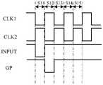
下面以晶体管M1至M8均为P型薄膜晶体管为例,对图3所示的移位寄存器单元的工作过程进行示例性说明。其中,以第一级移位寄存器单元的工作过程为例进行说明。图4为图3提供的移位寄存器单元的工作时序图。如图3和图4所示,本示例性实施例的移位寄存器单元可以包括8个晶体管单元(M1至M8)、2个电容单元(C1和C2)、3个输入端(INPUT、CLK1、CLK2)、1个输出端(GP)和2个电压端(VGL、VGH)。其中,第一电压端VGL可以持续提供低电平信号,第二电压端VGH可以持续提供高电平信号。In the following, the operation process of the shift register unit shown in FIG. 3 will be exemplarily described by taking that the transistors M1 to M8 are all P-type thin film transistors as an example. Wherein, the working process of the first-stage shift register unit is taken as an example for description. FIG. 4 is a working timing diagram of the shift register unit provided in FIG. 3 . As shown in FIG. 3 and FIG. 4 , the shift register unit of this exemplary embodiment may include 8 transistor units (M1 to M8), 2 capacitor units (C1 and C2), 3 input terminals (INPUT, CLK1, CLK2), 1 output terminal (GP) and 2 voltage terminals (VGL, VGH). Wherein, the first voltage terminal VGL can continuously provide a low-level signal, and the second voltage terminal VGH can continuously provide a high-level signal.
在输入阶段S11,第一时钟信号端CLK1的输入信号为低电平,第一晶体管M1导通和第三晶体管M3导通。第一晶体管M1导通,且第一电压端VGL的输入信号为低电平,则第一控制节点P1的电位被拉低;第三晶体管M3导通,且信号输入端INPUT的输入信号为低电平,则第二控制节点P2的电位被拉低,使得第二晶体管M2导通,可以进一步保证第一控制节点P1的电位被拉低。由于第一控制节点P1的电位被拉低,第四晶体管M4和第八晶体管M8导通。第八晶体管M8导通,且第二电压端VGH的输入信号为高电平,则输出端GP的电位被拉高。第二时钟信号端CLK2的输入信号为高电平,则第五晶体管M5截止。第一电压端VGL的输入信号为低电平,则第六晶体管M6导通,第三控制节点P3的电位被第二控制节点P2的电位拉低,使得第七晶体管M7导通,可以进一步保证输出端GP的电位被拉高。In the input stage S11, the input signal of the first clock signal terminal CLK1 is at a low level, and the first transistor M1 is turned on and the third transistor M3 is turned on. The first transistor M1 is turned on, and the input signal of the first voltage terminal VGL is at a low level, the potential of the first control node P1 is pulled down; the third transistor M3 is turned on, and the input signal of the signal input terminal INPUT is low level, the potential of the second control node P2 is pulled down, so that the second transistor M2 is turned on, which can further ensure that the potential of the first control node P1 is pulled down. Since the potential of the first control node P1 is pulled down, the fourth transistor M4 and the eighth transistor M8 are turned on. The eighth transistor M8 is turned on, and the input signal of the second voltage terminal VGH is at a high level, so the potential of the output terminal GP is pulled up. When the input signal of the second clock signal terminal CLK2 is at a high level, the fifth transistor M5 is turned off. When the input signal of the first voltage terminal VGL is at a low level, the sixth transistor M6 is turned on, and the potential of the third control node P3 is pulled down by the potential of the second control node P2, so that the seventh transistor M7 is turned on, which can further ensure The potential of the output terminal GP is pulled high.
在输出阶段S12,第一时钟信号端CLK1的输入信号为高电平,第一晶体管M1和第三晶体管M3截止,第二控制节点P2的电位保持为低电平,第二晶体管M2导通,第一控制节点P1的电位保持在高电平。而且,在第二电容C2的作用下,可以进一步保证第一控制节点P2保持在高电平。由于第一控制节点P2的电位保持在高电平,第四晶体管M4和第八晶体管M8截止。第二时钟信号端CLK2的输入信号为低电平,第五晶体管M5导通。第一电压端VGL的输入信号为低电平,第六晶体管M6导通,第三控制节点P3的电位进一步被第二控制节点P2拉低,使得第七晶体管M7导通,输出端GP的电位被第二时钟信号端CLK2的输入信号拉低。In the output stage S12, the input signal of the first clock signal terminal CLK1 is at a high level, the first transistor M1 and the third transistor M3 are turned off, the potential of the second control node P2 is kept at a low level, and the second transistor M2 is turned on, The potential of the first control node P1 is maintained at a high level. Moreover, under the action of the second capacitor C2, it can further ensure that the first control node P2 is kept at a high level. Since the potential of the first control node P2 remains at a high level, the fourth transistor M4 and the eighth transistor M8 are turned off. The input signal of the second clock signal terminal CLK2 is at a low level, and the fifth transistor M5 is turned on. The input signal of the first voltage terminal VGL is at a low level, the sixth transistor M6 is turned on, and the potential of the third control node P3 is further pulled down by the second control node P2, so that the seventh transistor M7 is turned on, and the potential of the output terminal GP is turned on. Pulled down by the input signal of the second clock signal terminal CLK2.
在复位阶段S13,第一时钟信号端CLK1的输入信号为低电平,第一晶体管M1和第三晶体管M3导通,第一控制节点P1的电位被第一电压端VGL的输入信号拉低;信号输入端INPUT的输入信号为高电平,第二控制节点P2的电位被拉高,使得第二晶体管M2截止。由于第一控制节点P1的电位被拉低,第四晶体管M4和第八晶体管M8导通。第八晶体管M8导通,且第二电压端VGH的输入信号为高电平,则输出端GP的电位可以保持在高电平。第二时钟信号端CLK2的输入信号为高电平,第五晶体管M5截止。第一电压端VGL的输入信号为低电平,第六晶体管M6导通,第三控制节点P3的电位被第二控制节点P2拉高,使得第七晶体管M7截止。In the reset phase S13, the input signal of the first clock signal terminal CLK1 is at a low level, the first transistor M1 and the third transistor M3 are turned on, and the potential of the first control node P1 is pulled down by the input signal of the first voltage terminal VGL; The input signal of the signal input terminal INPUT is at a high level, and the potential of the second control node P2 is pulled up, so that the second transistor M2 is turned off. Since the potential of the first control node P1 is pulled down, the fourth transistor M4 and the eighth transistor M8 are turned on. When the eighth transistor M8 is turned on, and the input signal of the second voltage terminal VGH is at a high level, the potential of the output terminal GP can be maintained at a high level. The input signal of the second clock signal terminal CLK2 is at a high level, and the fifth transistor M5 is turned off. The input signal of the first voltage terminal VGL is at a low level, the sixth transistor M6 is turned on, and the potential of the third control node P3 is pulled up by the second control node P2, so that the seventh transistor M7 is turned off.
在第一保持阶段S14,第一时钟信号端CLK1的输入信号为高电平,第一开关晶体管M4和第三开关晶体管M3截止,信号输入端INPUT的输入信号为高电平,第二控制节点P2的电位保持为高电平,第二晶体管M2截止,第一控制节点P1的电位保持在低电平。由于第一控制节点P1的电位保持在低电平,第四晶体管M4和第八晶体管M8导通,输出端GP的电位保持为高电平。第二时钟信号端CLK2的输入信号为低电平,第五晶体管M5导通。第一电压端VGL的电位为低电平,第六晶体管M6导通,第三控制节点P3的电位保持在高电平,第七晶体管M7截止。In the first hold stage S14, the input signal of the first clock signal terminal CLK1 is at a high level, the first switch transistor M4 and the third switch transistor M3 are turned off, the input signal of the signal input terminal INPUT is at a high level, and the second control node The potential of P2 is kept at a high level, the second transistor M2 is turned off, and the potential of the first control node P1 is kept at a low level. Since the potential of the first control node P1 is kept at a low level, the fourth transistor M4 and the eighth transistor M8 are turned on, and the potential of the output terminal GP is kept at a high level. The input signal of the second clock signal terminal CLK2 is at a low level, and the fifth transistor M5 is turned on. The potential of the first voltage terminal VGL is at a low level, the sixth transistor M6 is turned on, the potential of the third control node P3 is maintained at a high level, and the seventh transistor M7 is turned off.
在第二保持阶段S15,第一时钟信号端CLK1的输入信号为低电平,第一晶体管M1和第三晶体管M3导通,信号输入端INPUT的输入信号为高电平,第二控制节点P2的电位保持为高电平,第二晶体管M2截止,第一控制节点P1的电位保持在低电平。由于第一控制节点P1的电位保持在低电平,第四晶体管M4和第八晶体管M7导通,输出端GP的电位保持为高电平。第二时钟信号端CLK2的输入信号为高电平,第五晶体管M5截止。第一电压端VGL的电位为低电平,第六晶体管M6导通,第三控制节点P3的电位保持在高电平,第七晶体管M7截止。In the second holding stage S15, the input signal of the first clock signal terminal CLK1 is at a low level, the first transistor M1 and the third transistor M3 are turned on, the input signal of the signal input terminal INPUT is at a high level, and the second control node P2 The potential of the first control node P1 is kept at a high level, the second transistor M2 is turned off, and the potential of the first control node P1 is kept at a low level. Since the potential of the first control node P1 is kept at a low level, the fourth transistor M4 and the eighth transistor M7 are turned on, and the potential of the output terminal GP is kept at a high level. The input signal of the second clock signal terminal CLK2 is at a high level, and the fifth transistor M5 is turned off. The potential of the first voltage terminal VGL is at a low level, the sixth transistor M6 is turned on, the potential of the third control node P3 is maintained at a high level, and the seventh transistor M7 is turned off.
在第二保持阶段之后,可以重复第一保持阶段和第二保持阶段直至信号输入端INPUT的输入信号为低电平,再从输入阶段重新开始。After the second hold phase, the first hold phase and the second hold phase may be repeated until the input signal at the signal input terminal INPUT is at a low level, and then restart from the input phase.
在本示例性实施例中,至少一个子像素可以包括:发光元件以及用于驱动发光元件发光的驱动电路。驱动电路可以包括多个晶体管和存储电容。在本示例中,子像素的驱动电路可以为7T1C结构(即包括七个晶体管和一个电容)。然而,本实施例对此并不限定。在一些示例中,子像素的驱动电路可以为2T1C、或者3T1C等结构。In this exemplary embodiment, at least one sub-pixel may include: a light-emitting element and a driving circuit for driving the light-emitting element to emit light. The driver circuit may include a plurality of transistors and storage capacitors. In this example, the driving circuit of the sub-pixel may be a 7T1C structure (ie, including seven transistors and one capacitor). However, this embodiment does not limit this. In some examples, the driving circuit of the sub-pixel may be a 2T1C or 3T1C structure.
图5为本公开至少一实施例的驱动电路的等效电路图。如图5所示,本示例性实施例的驱动电路可以包括:第一开关晶体管T1至第六开关晶体管T6、驱动晶体管DTFT以及存储电容Cst。FIG. 5 is an equivalent circuit diagram of a driving circuit according to at least one embodiment of the present disclosure. As shown in FIG. 5 , the driving circuit of the present exemplary embodiment may include: first to sixth switching transistors T1 to T6 , a driving transistor DTFT, and a storage capacitor Cst.
在本示例性实施例中,驱动晶体管DTFT的控制极与第一节点N1连接,驱动晶体管T3的第一极与第二节点N2连接,驱动晶体管T3的第二极与第三节点N3连接。第一开关晶体管T1的控制极与扫描线G连接,第一开关晶体管T1的第一极与数据线D连接,第一开关晶体管T1的第二极与第二节点N2连接。第二开关晶体管T2的控制极与扫描线G连接,第二开关晶体管T2的第一极与第一节点N1连接,第二开关晶体管T2的第二极与第三节点N3连接。第三开关晶体管T3的控制极与发光控制线EM连接,第三开关晶体管T3的第一极与第一电源线VDD连接,第三开关晶体管T3的第二极与第二节点N2连接。第四开关晶体管T4的控制极与发光控制线EM连接,第四开关晶体管T4的第一极与第三节点N3连接,第四开关晶体管T4的第二极与发光元件EL的阳极连接。第五开关晶体管T5的控制极与复位信号线RST连接,第五开关晶体管T5的第一极与初始信号线Vint,第五开关晶体管T5的第二极与第一节点N1连接。第六开关晶体管T6的控制极与复位信号线RST连接,第六开关晶体管T6的第一极与初始信号线Vint连接,第六开关晶体管T6的第二极与发光元件EL的阳极连接。存储电容Cst的第一电极与第一节点N1连接,存储电容Cst的第二电极与第一电源线VDD连接。发光元件EL的阴极与第二电源线VSS连接。In this exemplary embodiment, the control electrode of the driving transistor DTFT is connected to the first node N1, the first electrode of the driving transistor T3 is connected to the second node N2, and the second electrode of the driving transistor T3 is connected to the third node N3. The control electrode of the first switch transistor T1 is connected to the scan line G, the first electrode of the first switch transistor T1 is connected to the data line D, and the second electrode of the first switch transistor T1 is connected to the second node N2. The control electrode of the second switching transistor T2 is connected to the scan line G, the first electrode of the second switching transistor T2 is connected to the first node N1, and the second electrode of the second switching transistor T2 is connected to the third node N3. The control electrode of the third switch transistor T3 is connected to the light-emitting control line EM, the first electrode of the third switch transistor T3 is connected to the first power line VDD, and the second electrode of the third switch transistor T3 is connected to the second node N2. The control electrode of the fourth switching transistor T4 is connected to the light emitting control line EM, the first electrode of the fourth switching transistor T4 is connected to the third node N3, and the second electrode of the fourth switching transistor T4 is connected to the anode of the light emitting element EL. The control pole of the fifth switch transistor T5 is connected to the reset signal line RST, the first pole of the fifth switch transistor T5 is connected to the initial signal line Vint, and the second pole of the fifth switch transistor T5 is connected to the first node N1. The control electrode of the sixth switching transistor T6 is connected to the reset signal line RST, the first electrode of the sixth switching transistor T6 is connected to the initial signal line Vint, and the second electrode of the sixth switching transistor T6 is connected to the anode of the light emitting element EL. The first electrode of the storage capacitor Cst is connected to the first node N1, and the second electrode of the storage capacitor Cst is connected to the first power line VDD. The cathode of the light-emitting element EL is connected to the second power supply line VSS.
下面以第一开关晶体管T1至第六开关晶体管T6以及驱动晶体管DTFT均为P型薄膜晶体管为例,对图5提供的驱动电路的工作过程进行示例性说明。图6为图5提供的驱动电路的工作时序图。如图5所示,本示例性实施例中涉及的驱动电路可以包括:6个开关晶体管(T1至T6),1个驱动晶体管(DTFT)、1个电容单元(Cst)、5个信号输入端(D、G、EM、RST和Vint)、2个电源端(VDD和VSS)。示例性地,第一电源线VDD可以持续提供高电平信号,第二电源线VSS可以持续提供低电平信号。The working process of the driving circuit provided in FIG. 5 is exemplarily described below by taking the example that the first switching transistor T1 to the sixth switching transistor T6 and the driving transistor DTFT are all P-type thin film transistors. FIG. 6 is a working timing diagram of the driving circuit provided in FIG. 5 . As shown in FIG. 5 , the driving circuit involved in this exemplary embodiment may include: 6 switching transistors (T1 to T6), 1 driving transistor (DTFT), 1 capacitor unit (Cst), and 5 signal input terminals (D, G, EM, RST and Vint), 2 power terminals (VDD and VSS). Exemplarily, the first power line VDD may continuously provide a high-level signal, and the second power line VSS may continuously provide a low-level signal.
在复位阶段S21,扫描线G输入高电平信号,第一开关晶体管T1和第二开关晶体管T2截止。发光控制线EM输入高电平信号,第三开关晶体管T3和第四开关晶体管T4截止。复位信号线RST输入低电平信号,第五开关晶体管T5和第六开关晶体管T6导通,向第一节点N1和第四节点N4提供初始信号线Vint输入的信号,以对第一节点N1和第四节点N4进行复位,从而消除上一帧信号的影响。In the reset phase S21, a high level signal is input to the scan line G, and the first switching transistor T1 and the second switching transistor T2 are turned off. A high-level signal is input to the light-emitting control line EM, and the third switch transistor T3 and the fourth switch transistor T4 are turned off. The reset signal line RST inputs a low-level signal, the fifth switch transistor T5 and the sixth switch transistor T6 are turned on, and the first node N1 and the fourth node N4 are provided with the signal input by the initial signal line Vint, so as to connect the first node N1 and the fourth node N4 The fourth node N4 is reset, thereby eliminating the influence of the signal of the previous frame.
在写入阶段S22,复位信号线RST输入高电平信号,第五开关晶体管T5和第六开关晶体管T6截止。发光控制线EM输入高电平信号,第三开关晶体管T3和第四开关晶体管T4截止。扫描线G输入低电平信号,第一开关晶体管T1和第二开关晶体管T2导通。第一开关晶体管M1导通,向第二节点N2提供数据线DATA输入的数据信号,此时,第二节点N2的电位Vn2=Vdata,Vdata为数据信号的电压值。第二开关晶体管M2导通,将第一节点N1和第三节点N3连通,即将驱动晶体管DTFT的控制极与第二极连通,以将传输至第二节点N2的数据信号和驱动晶体管DTFT的阈值电压Vth(即补偿信号)写入第一节点N1,同时对存储电容Cst进行充电,此时,第一节点N1的电位Vn1=Vdata-Vth。通过写入阶段S21可以将数据信号写入驱动晶体管DTFT的控制极并对驱动晶体管DTFT的阈值电压进行补偿,以在发光阶段消除驱动晶体管DTFT的阈值电压对驱动电流的影响。In the writing phase S22, a high level signal is input to the reset signal line RST, and the fifth switching transistor T5 and the sixth switching transistor T6 are turned off. A high-level signal is input to the light-emitting control line EM, and the third switch transistor T3 and the fourth switch transistor T4 are turned off. A low-level signal is input to the scan line G, and the first switch transistor T1 and the second switch transistor T2 are turned on. The first switching transistor M1 is turned on to provide the data signal input by the data line DATA to the second node N2. At this time, the potential of the second node N2 is Vn2=Vdata, and Vdata is the voltage value of the data signal. The second switching transistor M2 is turned on to connect the first node N1 and the third node N3, that is, the control electrode of the driving transistor DTFT is connected to the second electrode, so as to connect the data signal transmitted to the second node N2 and the threshold value of the driving transistor DTFT The voltage Vth (ie, the compensation signal) is written into the first node N1, and the storage capacitor Cst is charged at the same time. At this time, the potential of the first node N1 is Vn1=Vdata-Vth. Through the writing stage S21, the data signal can be written into the gate electrode of the driving transistor DTFT and the threshold voltage of the driving transistor DTFT can be compensated to eliminate the influence of the threshold voltage of the driving transistor DTFT on the driving current in the light-emitting stage.
在发光阶段S23,复位信号线RST输入高电平信号,第五开关晶体管T5和第六开关晶体管T6截止。扫描线G输入高电平信号,第一开关晶体管T1和第二开关晶体管T2截止。发光控制线EM输入低电平信号,第三开关晶体管T3和第四开关晶体管T4导通。第三开关晶体管T3导通,向第二节点N2提供第一电源线VDD输入的信号,此时,Vn2=Vvdd。驱动晶体管DTFT在第一节点N1的信号(即数据信号和补偿信号)的作用下导通,并在第一电源线VDD提供的信号的作用下输出驱动电流,以驱动发光元件EL发光。其中,第一节点N1的电位在存储电容Cst的作用下保持在Vdata-Vth不变,则驱动晶体管DTFT的源栅电压可以为:In the light-emitting stage S23, a high-level signal is input to the reset signal line RST, and the fifth switching transistor T5 and the sixth switching transistor T6 are turned off. A high level signal is input to the scan line G, and the first switching transistor T1 and the second switching transistor T2 are turned off. A low-level signal is input to the light-emitting control line EM, and the third switch transistor T3 and the fourth switch transistor T4 are turned on. The third switching transistor T3 is turned on to provide the second node N2 with a signal input from the first power supply line VDD. At this time, Vn2=Vvdd. The driving transistor DTFT is turned on under the action of the signal of the first node N1 (ie, the data signal and the compensation signal), and outputs a driving current under the action of the signal provided by the first power line VDD to drive the light-emitting element EL to emit light. Wherein, the potential of the first node N1 remains unchanged at Vdata-Vth under the action of the storage capacitor Cst, then the source-to-gate voltage of the driving transistor DTFT can be:
Vsg=Vn2-Vn1=Vvdd-Vdata+Vth。Vsg=Vn2-Vn1=Vvdd-Vdata+Vth.
根据以下晶体管I-V曲线方程:According to the following transistor I-V curve equation:
I=K(Vsg-Vth)2=K(Vvdd-Vdata)2;I=K(Vsg-Vth)2 =K(Vvdd-Vdata)2 ;
其中,K为与驱动晶体管DTFT的工艺参数和几何尺寸有关的固定常数。Among them, K is a fixed constant related to the process parameters and geometric dimensions of the driving transistor DTFT.
由此可见,驱动电流与驱动晶体管DTFT的阈值电压无关,消除了阈值电压对发光元件EL的影响,从而可以提高显示均匀性和发光效率。It can be seen that the driving current has nothing to do with the threshold voltage of the driving transistor DTFT, which eliminates the influence of the threshold voltage on the light-emitting element EL, thereby improving display uniformity and luminous efficiency.
图7为本公开至少一实施例的显示基板的一个子像素的俯视图。图8为图7中Q-Q方向的剖面示意图。如图7和图8所示,本示例性实施例提供的显示基板的显示区域可以包括:基底30、依次设置在基底30上的半导体层、第一导电层、第二导电层、第三导电层、第四导电层以及第五导电层。其中,第一绝缘层32可以设置在半导体层和第一导电层之间,第二绝缘层34可以设置在第一导电层和第二导电层之间,第三绝缘层36可以设置在第二导电层和第三导电层之间,第四绝缘层38可以设置在第三导电层和第四导电层之间,第五绝缘层40可以设置在第四导电层和第五导电层之间。第五导电层可以包括发光元件的阳极41,第五导电层上还设置有发光元件的有机发光层43以及阴极44。7 is a top view of a sub-pixel of a display substrate according to at least one embodiment of the disclosure. FIG. 8 is a schematic cross-sectional view along the Q-Q direction in FIG. 7 . As shown in FIG. 7 and FIG. 8 , the display area of the display substrate provided by this exemplary embodiment may include: a
图9为本公开至少一实施例中形成半导体层后的显示基板的俯视图。如图7至图9所示,第五开关晶体管T5、第二开关晶体管T2、第一开关晶体管T1、驱动晶体管DTFT、第三开关晶体管T3、第四开关晶体管T4以及第六开关晶体管T6可以沿着如图9所示的半导体层形成。如图9所示,半导体层可以具有弯曲或弯折形状。半导体层可以包括:第一开关晶体管T1的有源层210、第二开关晶体管T2的有源层220、第三开关晶体管T3的有源层230、第四开关晶体管T4的有源层240、第五开关晶体管T5的有源层250、第六开关晶体管T6的有源层260以及驱动晶体管DTFT的有源层270。9 is a top view of a display substrate after forming a semiconductor layer according to at least one embodiment of the disclosure. As shown in FIGS. 7 to 9 , the fifth switching transistor T5, the second switching transistor T2, the first switching transistor T1, the driving transistor DTFT, the third switching transistor T3, the fourth switching transistor T4 and the sixth switching transistor T6 may be A semiconductor layer as shown in FIG. 9 is formed. As shown in FIG. 9, the semiconductor layer may have a curved or bent shape. The semiconductor layer may include: the
在本示例性实施例中,有源层的材料例如可以包括多晶硅或者金属氧化物。在一些示例中,有源层可以包括沟道区、第一掺杂区和第二掺杂区。沟道区可以不掺杂杂质,并具有半导体特性。第一掺杂区和第二掺杂区可以在沟道区的两侧,并且掺杂有杂质,并因此具有导电性。杂质可以根据晶体管的类型而变化。In the present exemplary embodiment, the material of the active layer may include polysilicon or metal oxide, for example. In some examples, the active layer may include a channel region, a first doped region, and a second doped region. The channel region may not be doped with impurities and have semiconductor characteristics. The first doped region and the second doped region may be on both sides of the channel region, and are doped with impurities and thus have conductivity. Impurities can vary depending on the type of transistor.
在本示例性实施例中,有源层的第一掺杂区或第二掺杂区可以被解释为晶体管的源电极或漏电极。例如,驱动晶体管的源电极可以与有源层的沟道区的周边、掺杂有杂质的第一掺杂区对应;驱动晶体管的漏电极可以与有源层的沟道区的周边、掺杂有杂质的第二掺杂区对应。另外,晶体管之间的有源层的部分可以被解释为掺杂有杂质的布线,可以用于电连接晶体管。In the present exemplary embodiment, the first doped region or the second doped region of the active layer may be interpreted as a source electrode or a drain electrode of a transistor. For example, the source electrode of the driving transistor may correspond to the periphery of the channel region of the active layer and the first doped region doped with impurities; the drain electrode of the driving transistor may correspond to the periphery of the channel region of the active layer, the first doped region doped with impurities The second doped region with impurities corresponds. In addition, the portion of the active layer between the transistors can be interpreted as a wiring doped with impurities, which can be used to electrically connect the transistors.
图10为本公开至少一实施例中形成第一导电层后的显示基板的俯视图。如图7至图10所示,第一导电层可以包括:发光控制线EM、第一开关晶体管T1的控制极211、第二开关晶体管T2的控制极221a和221b、第三开关晶体管T3的控制极231、第四开关晶体管T4的控制极241、第五开关晶体管T5的控制极251a和251b、第六开关晶体管T6的控制极261、驱动晶体管DTFT的控制极271以及存储电容Cst的第一电极281。10 is a top view of a display substrate after forming a first conductive layer according to at least one embodiment of the disclosure. As shown in FIG. 7 to FIG. 10 , the first conductive layer may include: a light-emitting control line EM, a
在本示例性实施例中,驱动晶体管DTFT的控制极271和存储电容Cst的第一电极281可以为一体结构。发光控制线EM、第三开关晶体管T3的控制极231以及第四开关晶体管T4的控制极241可以为一体结构。第二开关晶体管T2的控制极221a和221b可以为一体结构。第五开关晶体管T5的控制极251a和251b可以为一体结构。In this exemplary embodiment, the
图11为本公开至少一实施例中形成第二导电层后的显示基板的俯视图。如图7至图11所示,第二导电层可以包括:存储电容Cst的第二电极282。在本示例性实施例中,存储电容Cst的第二电极282可以具有一镂空区域H。驱动晶体管DTFT的控制极271在基底30上正投影可以覆盖镂空区域H在基底30上的正投影。在一些示例中,镂空区域H在基底30上的正投影可以为圆形或多边形。然而,本实施例对此并不限定。11 is a top view of a display substrate after forming a second conductive layer according to at least one embodiment of the disclosure. As shown in FIG. 7 to FIG. 11 , the second conductive layer may include: the
图12为本公开至少一实施例中形成第三导电层后的显示基板的俯视图。如图7至图12所示,第三导电层可以包括:扫描线G、复位信号线RSTa和RSTb、第一开关晶体管T1的第一极212、第二开关晶体管T2的第一极222、第三开关晶体管T3的第一极232、第四开关晶体管T4的第二极243、第五开关晶体管T5的第一极252以及第六开关晶体管T6的第一极262。12 is a top view of a display substrate after forming a third conductive layer in at least one embodiment of the disclosure. As shown in FIG. 7 to FIG. 12 , the third conductive layer may include: a scan line G, reset signal lines RSTa and RSTb, a
在本示例性实施例中,扫描线G可以平行于复位信号线RSTa和RSTb,且扫描线G与复位信号线RSTa之间的距离可以小于扫描线G与复位信号线RSTb之间的距离。In the present exemplary embodiment, the scan line G may be parallel to the reset signal lines RSTa and RSTb, and the distance between the scan line G and the reset signal line RSTa may be smaller than the distance between the scan line G and the reset signal line RSTb.
在本示例性实施例中,扫描线G可以通过第三绝缘层36和第二绝缘层34中的第一过孔K2与第一开关晶体管T1的控制极211连接。扫描线G可以通过第三绝缘层36和第二绝缘层34中的第一过孔K3与第二开关晶体管T1的控制极221a和221b连接。复位信号线RSTa可以通过第三绝缘层36和第二绝缘层34中的第一过孔K10与第五开关晶体管T5的控制极251a和251b连接。复位信号线RSTb可以通过第三绝缘层36和第二绝缘层34中的第一过孔K11与第六开关晶体管T6的控制极261连接。In the present exemplary embodiment, the scan line G may be connected to the
在本示例性实施例中,扫描线G在基底30上的正投影可以覆盖第一开关晶体管T1的控制极211在基底30上的正投影,并可以与第二开关晶体管T2的控制极221a和221b在基底30上的正投影部分交叠。复位信号线RSTa在基底30上的正投影与第五开关晶体管T5的控制极251a和251b在基底30上的正投影可以部分交叠。复位信号线RSTb在基底30上的正投影可以覆盖第六开关晶体管T6的控制极261在基底30上的正投影。In the present exemplary embodiment, the orthographic projection of the scan line G on the
在本示例性实施例中,扫描线G在基底30上的正投影可以覆盖第一过孔K2和K3在基底30上的正投影。复位信号线RSTa在基底30上的正投影可以覆盖第一过孔K10在基底30上的正投影。复位信号线RSTb在基底30上的正投影可以覆盖第一过孔K11在基底30上的正投影。In this exemplary embodiment, the orthographic projection of the scan line G on the
在本示例性实施例中,第一开关晶体管T1的第一极212可以通过第三绝缘层36、第二绝缘层34和第一绝缘层32中的第三过孔K1与第一开关晶体管T1的有源层210的第一掺杂区210b连接。第二开关晶体管T2的第一极222可以通过第三绝缘层36、第二绝缘层34和第一绝缘层32中的第三过孔K4与第二开关晶体管T2的有源层220的第一掺杂区220b连接,还可以通过第三绝缘层36和第二绝缘层34中的第一过孔K5与驱动晶体管DTFT的控制极271连接。第三开关晶体管T3的第一极232可以通过第三绝缘层36、第二绝缘层34和第一绝缘层32中的第三过孔K7与第三开关晶体管T3的有源层230的第一掺杂区230b连接,还可以通过第三绝缘层36中的第四过孔K6与存储电容Cst的第二电极282连接。第四开关晶体管T4的第二极243可以通过第三绝缘层36、第二绝缘层34和第一绝缘层32中的第三过孔K8与第四开关晶体管T4的有源层240的第二掺杂区240c连接。第五开关晶体管T5的第一极252可以通过第三绝缘层36、第二绝缘层34和第一绝缘层32中的第三过孔K9与第五开关晶体管T5的有源层250的第一掺杂区250b连接。第六开关晶体管T6的第一极262可以通过第三绝缘层36、第二绝缘层34和第一绝缘层32中的第三过孔K12与第六开关晶体管T6的有源层260的第一掺杂区260b连接。In the present exemplary embodiment, the
图13为本公开至少一实施例中形成第四导电层的俯视图。如图7至图13所示,第四导电层可以包括:连接电极291、数据线D、第一电源线VDD以及初始信号线Vint。其中,数据线D、第一电源线VDD以及初始信号线Vint的延伸方向相互平行,均平行于第二方向。第一电源线VDD沿第一方向的宽度可以大于初始信号线Vint沿第一方向的宽度,初始信号线Vint沿第一方向的宽度可以大于第一电源线VDD沿第一方向的宽度。13 is a top view of forming a fourth conductive layer in at least one embodiment of the present disclosure. As shown in FIGS. 7 to 13 , the fourth conductive layer may include: a
在本示例性实施例中,数据线D可以通过第四绝缘层38中的第二过孔K14与第一开关晶体管T1的第一极212连接。第一电源线VDD可以通过第四绝缘层38中的第二过孔K17、K18和K19与第三开关晶体管T3的第一极232连接。在本示例性实施例中,通过在第四绝缘层38设置多个第二过孔连接第三开关晶体管T3的第一极232和第一电源线VDD,可以确保提供稳定的电源信号。初始信号线Vint可以通过第四绝缘层38中的第二过孔K15与第五开关晶体管T5的第一极252连接,可以通过第四绝缘层38中的第二过孔K16与第六开关晶体管T6的第一极262连接。In the present exemplary embodiment, the data line D may be connected to the
在本示例性实施例中,连接电极291可以通过第四绝缘层38中的第二过孔K20与第四开关晶体管T4的第二极243连接。连接电极291还可以通过第五绝缘层40中的第五过孔K21与发光元件的阳极41连接。In the present exemplary embodiment, the
在本示例性实施例中,存储电容Cst可以包括:第一电极281和第二电极282,且两者之间具有第二绝缘层34。存储电容Cst的第一电极281还可以作为驱动晶体管DTFT的控制极。在本示例中,驱动晶体管DTFT的控制极271和存储电容Cst的第一电极281可以为一体结构。In this exemplary embodiment, the storage capacitor Cst may include a
在本示例性实施例中,驱动晶体管DTFT可以包括:有源层270和控制极271。驱动晶体管DTFT的有源层270可以包括:第一掺杂区270b、第二掺杂区270c以及连接第一掺杂区270b和第二掺杂区270c的沟道区270a。控制极271还可以作为存储电容Cst的第一电极281。驱动晶体管DTFT的有源层270的沟道区270a在基底30上的正投影与控制极271在基底30上的正投影可以重叠。第一掺杂区270b和第二掺杂区270c相对于沟道区270a在两个方向上延伸。驱动晶体管DTFT的第一掺杂区270b连接至第一开关晶体管T1的有源层210的第二掺杂区210c。驱动晶体管DTFT的第二掺杂区270c连接至第二开关晶体管T2的有源层220的第二掺杂区220c和第四开关晶体管T4的有源层240的第一掺杂区240b。In the present exemplary embodiment, the driving transistor DTFT may include an
在本示例性实施例中,第一开关晶体管T1可以包括:有源层210、控制极211以及第一极212。第一开关晶体管T1的有源层210可以包括:第一掺杂区210b、第二掺杂区210c以及连接第一掺杂区210b和第二掺杂区210c的沟道区210a。第一开关晶体管T1的第二掺杂区210c可以连接至驱动晶体管DTFT的有源层270的第一掺杂区270b。第一开关晶体管T1的第一掺杂区210b可以通过第一绝缘层32、第二绝缘层34和第三绝缘层36中的第三过孔K1与第一开关晶体管T1的第一极212连接。第一开关晶体管T1的第一极212可以通过第四绝缘层38中的第二过孔K14与数据线D连接。第一开关晶体管T1的控制极211可以通过第二绝缘层34和第三绝缘层36中的第一过孔K2与扫描线G连接。In this exemplary embodiment, the first switching transistor T1 may include an
在本示例性实施例中,第二开关晶体管T2可以包括:有源层220、控制极221a和221b、第一极222。有源层220可以包括:沟道区220a1、220a2、220a3、第一掺杂区220b以及第二掺杂区220c。沟道区220a1对应控制极221a,沟道区220a3对应控制极221b,沟道区220a2位于220a1和220a3之间。第二开关晶体管T2的第一掺杂区220b可以连接至第五开关晶体管T5的第二掺杂区250c。第一掺杂区220b可以通过第一绝缘层32、第二绝缘层34和第三绝缘层36中的第三过孔K4与第二开关晶体管T2的第一极222连接。第二开关晶体管T2的第一极222可以通过第三绝缘层36和第二绝缘层34中的第一过孔K5与驱动晶体管DTFT的控制极271连接。第二开关晶体管T2的控制极221a和221b可以通过第二绝缘层34和第三绝缘层36中的第一过孔K3与扫描线G连接。在本示例中,第二开关晶体管T2通过设置双控制极,可以用于防止和减少漏电流的发生。In the present exemplary embodiment, the second switching transistor T2 may include: an
在本示例性实施例中,第三开关晶体管T3可以包括:有源层230、控制极231以及第一极232。有源层230可以包括:沟道区230a、第一掺杂区230b以及第二掺杂区230c。第三开关晶体管T3的第一掺杂区230b可以通过第一绝缘层32、第二绝缘层34和第三绝缘层36中的第三过孔K7连接至第一极232。第三开关晶体管T3的第一极232可以通过第四绝缘层38中的第二过孔K17、K18和K19连接至第一电源线VDD。第三开关晶体管T3的第一极232还可以通过第三绝缘层36中的第四过孔K6连接至存储电容Cst的第二电极282。第三开关晶体管T3的控制极231与发光控制线EM可以为一体结构。In this exemplary embodiment, the third switching transistor T3 may include an
在本示例性实施例中,第四开关晶体管T4可以包括:有源层240、控制极241以及第二极243。第四开关晶体管T4的有源层240可以包括:沟道区240a、第一掺杂区240b以及第二掺杂区240c。第四开关晶体管T4的第一掺杂区240b可以分别与驱动晶体管DTFT的第二掺杂区270c以及第二开关晶体管T2的第二掺杂区220c连接。第四开关晶体管T4的第二掺杂区240c可以通过第一绝缘层32、第二绝缘层34以及第三绝缘层36中的第三过孔K8与第四开关晶体管T4的第二极243连接。第四开关晶体管T4的第二极243可以通过第四绝缘层38中的第二过孔K20与连接电极291连接。连接电极291可以通过第五绝缘层40中的第五过孔K21与发光元件的阳极41连接。In this exemplary embodiment, the fourth switching transistor T4 may include an
在本示例性实施例中,第五开关晶体管T5可以包括:有源层250、控制极251a、251b以及第一极252。有源层250可以包括:沟道区250a1、250a2、220a3、第一掺杂区250b以及第二掺杂区250c。沟道区250a1对应控制极251a,沟道区250a3对应控制极251b,沟道区250a2位于250a1和250a3之间。第一掺杂区250b可以连接至第二开关晶体管T2的第一掺杂区220b。第五开关晶体管T5的第一掺杂区250b可以通过第一绝缘层32、第二绝缘层34和第三绝缘层36中的第三过孔K9与第二极252连接。第五开关晶体管T5的控制极251a和251b可以通过第二绝缘层34和第三绝缘层36中的第一过孔K10与复位信号线RSTa连接。在本示例中,第五开关晶体管T5通过设置双控制极,可以用于防止和减少漏电流的发生。In the present exemplary embodiment, the fifth switching transistor T5 may include an
在本示例性实施例中,第六开关晶体管T6可以包括:有源层260、控制极261以及第一极262。有源层260可以包括:沟道区260a、第一掺杂区260b以及第二掺杂区260c。第六开关晶体管T6的第一掺杂区260b可以通过第一绝缘层32、第二绝缘层34和第三绝缘层36中的第三过孔K12与第一极262连接。第六开关晶体管T6的第一极262可以通过第四绝缘层38中的第二过孔K16与初始信号线Vint连接。第六开关晶体管T6的第二掺杂区260c可以与第四开关晶体管T4的第二掺杂区240c连接。第六开关晶体管T6的控制极261可以通过第二绝缘层34和第三绝缘层36中的第一过孔K11与复位信号线RSTb连接。In the present exemplary embodiment, the sixth switching transistor T6 may include an
图14为本公开至少一实施例的显示基板中多个子像素的俯视图。如图14所示,一行子像素可以与同一行的复位信号线RSTa、RSTb以及同一行的扫描线G连接,一列子像素可以与同一列的数据线D以及同一列的第一电线VDD连接。其中,多个子像素的第五开关晶体管T5的第一极252可以为一体结构,通过第二过孔K15与初始信号线Vint连接。多个子像素的第六开关晶体管T6的第一极262可以为一体结构,通过第二过孔K16与初始信号线Vint连接。在本示例中,每行子像素可以共用一个初始信号线Vint。然而,本实施例对此并不限定。14 is a top view of a plurality of sub-pixels in a display substrate according to at least one embodiment of the disclosure. As shown in FIG. 14 , a row of sub-pixels can be connected to the reset signal lines RSTa and RSTb of the same row and the scan line G of the same row, and a column of sub-pixels can be connected to the data line D of the same column and the first wire VDD of the same column. Wherein, the
在本示例性实施例中,多个子像素的存储电容Cst的第二电极282可以为一体结构。然而,本实施例对此并不限定。在一些示例中,多个子像素的存储电容Cst的第二电极可以为直接接触的独立结构。通过设置多个子像素的存储电容的第二电极直接接触,可以在多个子像素之间传递稳定的电源信号。In the present exemplary embodiment, the
下面参照图7至图14对本示例性实施例的显示基板的制备过程进行举例说明。本实施例中所说的“构图工艺”包括沉积膜层、涂覆光刻胶、掩模曝光、显影、刻蚀、剥离光刻胶等处理,是已知成熟的制备工艺。沉积可采用溅射、蒸镀、化学气相沉积等已知工艺,涂覆可采用已知的涂覆工艺,刻蚀可采用已知的方法,在此不做限定。在本实施例的描述中,需要理解的是,“薄膜”是指将某一种材料在基底上利用沉积或其它工艺制作出的一层薄膜。The manufacturing process of the display substrate of the present exemplary embodiment will be exemplified below with reference to FIGS. 7 to 14 . The "patterning process" mentioned in this embodiment includes processes such as film deposition, photoresist coating, mask exposure, development, etching, and photoresist stripping, and is a well-known and mature preparation process. The deposition can use known processes such as sputtering, evaporation, and chemical vapor deposition, the coating can use a known coating process, and the etching can use a known method, which is not limited herein. In the description of this embodiment, it should be understood that "thin film" refers to a layer of thin film made by depositing a certain material on a substrate or by other processes.
本示例性实施例的显示基板的制备过程可以包括以下步骤。The manufacturing process of the display substrate of the present exemplary embodiment may include the following steps.
步骤100、提供基底,在基底上沉积半导体薄膜,采用构图工艺对半导体薄膜进行处理形成半导体层,如图9所示。Step 100 , providing a substrate, depositing a semiconductor thin film on the substrate, and using a patterning process to process the semiconductor thin film to form a semiconductor layer, as shown in FIG. 9 .
在本示例性实施例中,基底可以为刚性衬底或柔性衬底。刚性衬底可以包括玻璃、金属箔片中的一种或多种。柔性衬底可以包括聚对苯二甲酸乙二醇酯、对苯二甲酸乙二醇酯、聚醚醚酮、聚苯乙烯、聚碳酸酯、聚芳基酸酯、聚芳酯、聚酰亚胺、聚氯乙烯、聚乙烯、纺织纤维中的一种或多种。In this exemplary embodiment, the substrate may be a rigid substrate or a flexible substrate. The rigid substrate may include one or more of glass, metal foil. Flexible substrates may include polyethylene terephthalate, polyethylene terephthalate, polyether ether ketone, polystyrene, polycarbonate, polyarylate, polyarylate, polyimide One or more of amine, polyvinyl chloride, polyethylene, textile fibers.
在本示例性实施例中,半导体层的制作材料可以为多晶硅或者金属氧化物,本公开实施例对此不作任何限定。In this exemplary embodiment, a material for fabricating the semiconductor layer may be polysilicon or metal oxide, which is not limited in this embodiment of the present disclosure.
步骤200、在半导体层上沉积第一绝缘薄膜,采用构图工艺对第一绝缘薄膜进行处理形成第一绝缘层,在第一绝缘层沉积第一导电薄膜,采用构图工艺对第一导电薄膜进行处理形成第一导电层,如图10所示。Step 200, depositing a first insulating film on the semiconductor layer, using a patterning process to process the first insulating film to form a first insulating layer, depositing a first conductive film on the first insulating layer, and using a patterning process to process the first conductive film A first conductive layer is formed, as shown in FIG. 10 .
在本示例性实施例中,第一导电层可以包括:发光控制线EM、第一开关晶体管T1的控制极211、第二开关晶体管T2的控制极221a和221b、第三开关晶体管T3的控制极231、第四开关晶体管T4的控制极241、第五开关晶体管T5的控制极251a和251b、第六开关晶体管T6的控制极261、驱动晶体管DTFT的控制极271以及存储电容Cst的第一电极281。In this exemplary embodiment, the first conductive layer may include: a light emission control line EM, a
在本示例性实施例中,第一导电薄膜可以采用金属材料,如银(Ag)、铜(Cu)、铝(Al)、钼(Mo)等,或上述金属的合金材料,如铝铌合金(AlNd)、钼铌合金(MoNb)等,可以是多层堆叠结构,如Mo/Cu/Mo、Mo/Al/Mo等,或可以是金属和透明导电材料形成的堆栈结构,如ITO/Ag/ITO等。第一绝缘薄膜可以采用硅氧化物(SiOx)、硅氮化物(SiNx)、氮氧化硅(SiON)等,或可以采用高介电常数(High k)材料,如氧化铝(AlOx)、氧化铪(HfOx)、氧化钽(TaOx)等,可以是单层、多层或复合层。通常,第一绝缘层32可以称为栅绝缘(GI)层。In this exemplary embodiment, the first conductive thin film may be made of metal materials, such as silver (Ag), copper (Cu), aluminum (Al), molybdenum (Mo), etc., or alloy materials of the above metals, such as aluminum-niobium alloys (AlNd), molybdenum-niobium alloy (MoNb), etc., can be a multi-layer stack structure, such as Mo/Cu/Mo, Mo/Al/Mo, etc., or can be a stack structure formed by metal and transparent conductive materials, such as ITO/Ag /ITO etc. The first insulating film can use silicon oxide (SiOx), silicon nitride (SiNx), silicon oxynitride (SiON), etc., or can use high dielectric constant (High k) materials, such as aluminum oxide (AlOx), hafnium oxide (HfOx), tantalum oxide (TaOx), etc., may be a single layer, a multi-layer or a composite layer. Generally, the first insulating
步骤300、在第一导电层上沉积第二绝缘薄膜,采用构图工艺对第二绝缘薄膜进行处理形成第二绝缘层,在第二绝缘层上沉积第二导电薄膜,采用构图工艺对第二导电薄膜进行处理形成第二导电层,如图11所示。Step 300, depositing a second insulating film on the first conductive layer, using a patterning process to process the second insulating film to form a second insulating layer, depositing a second conductive film on the second insulating layer, and applying a patterning process to the second conductive film The thin film is processed to form a second conductive layer, as shown in FIG. 11 .
在本示例性实施例中,第二导电层可以包括:存储电容Cst的第二电极282。In the present exemplary embodiment, the second conductive layer may include: the
在本示例性实施例中,第二导电薄膜可以采用金属材料,如银(Ag)、铜(Cu)、铝(Al)、钼(Mo)等,或上述金属的合金材料,如铝铌合金(AlNd)、钼铌合金(MoNb)等,可以是多层堆叠结构,如Mo/Cu/Mo、Mo/Al/Mo等,或可以是金属和透明导电材料形成的堆栈结构,如ITO/Ag/ITO等。第二绝缘薄膜可以采用硅氧化物(SiOx)、硅氮化物(SiNx)、氮氧化硅(SiON)等,或可以采用高介电常数(High k)材料,如氧化铝(AlOx)、氧化铪(HfOx)、氧化钽(TaOx)等,可以是单层、多层或复合层。通常,第二绝缘层34可以称为栅绝缘(GI)层。In this exemplary embodiment, the second conductive thin film may be made of metal materials, such as silver (Ag), copper (Cu), aluminum (Al), molybdenum (Mo), etc., or alloy materials of the above metals, such as aluminum-niobium alloys (AlNd), molybdenum-niobium alloy (MoNb), etc., can be a multi-layer stack structure, such as Mo/Cu/Mo, Mo/Al/Mo, etc., or can be a stack structure formed by metal and transparent conductive materials, such as ITO/Ag /ITO etc. The second insulating film can use silicon oxide (SiOx), silicon nitride (SiNx), silicon oxynitride (SiON), etc., or can use high dielectric constant (High k) materials such as aluminum oxide (AlOx), hafnium oxide (HfOx), tantalum oxide (TaOx), etc., may be a single layer, a multi-layer or a composite layer. Generally, the second insulating
步骤400、在第二导电层上形成沉积第三绝缘薄膜,采用构图工艺对第三绝缘薄膜进行处理形成第三绝缘层,在第三绝缘层上沉积第三导电薄膜,通过构图工艺对第三导电薄膜进行处理形成第三导电层,如图12所示。Step 400, forming and depositing a third insulating film on the second conductive layer, using a patterning process to process the third insulating film to form a third insulating layer, depositing a third conductive film on the third insulating layer, and applying a patterning process to the third insulating film. The conductive film is processed to form a third conductive layer, as shown in FIG. 12 .
在本示例性实施例中,第三导电层可以包括:扫描线G、复位信号线RSTa和RSTb、第一开关晶体管T1的第一极212、第二开关晶体管T2的第一极222、第三开关晶体管T3的第一极232、第四开关晶体管T4的第二极243、第五开关晶体管T5的第一极252以及第六开关晶体管T6的第一极262。In this exemplary embodiment, the third conductive layer may include: a scan line G, reset signal lines RSTa and RSTb, a
在本示例性实施例中,第三导电薄膜可以采用金属材料,如银(Ag)、铜(Cu)、铝(Al)、钛(Ti)等,或上述金属的合金材料,如铝铌合金(AlNd)、钼铌合金(MoNb)等,可以是多层堆叠结构,如Ti/Al/Ti等,或可以是金属和透明导电材料形成的堆栈结构,如ITO/Ag/ITO等。第三绝缘薄膜可以采用硅氧化物(SiOx)、硅氮化物(SiNx)、氮氧化硅(SiON)等,或可以采用高介电常数(High k)材料,如氧化铝(AlOx)、氧化铪(HfOx)、氧化钽(TaOx)等,可以是单层、多层或复合层。通常,第三绝缘层36可以称为层间绝缘层。In this exemplary embodiment, the third conductive thin film can be made of metal materials, such as silver (Ag), copper (Cu), aluminum (Al), titanium (Ti), etc., or alloy materials of the above metals, such as aluminum-niobium alloys (AlNd), molybdenum-niobium alloy (MoNb), etc., can be a multi-layer stack structure, such as Ti/Al/Ti, etc., or can be a stack structure formed of metal and transparent conductive materials, such as ITO/Ag/ITO, etc. The third insulating film may use silicon oxide (SiOx), silicon nitride (SiNx), silicon oxynitride (SiON), etc., or may use a high dielectric constant (High k) material, such as aluminum oxide (AlOx), hafnium oxide (HfOx), tantalum oxide (TaOx), etc., may be a single layer, a multi-layer or a composite layer. Generally, the third insulating
步骤500、在第三导电层上形成沉积第四绝缘薄膜,采用构图工艺对第四绝缘薄膜进行处理形成第四绝缘层,在第四绝缘层上沉积第四导电薄膜,通过构图工艺对第四导电薄膜进行处理形成第四导电层,如图13所示。Step 500, forming and depositing a fourth insulating film on the third conductive layer, using a patterning process to process the fourth insulating film to form a fourth insulating layer, depositing a fourth conductive film on the fourth insulating layer, and applying a patterning process to the fourth insulating film. The conductive film is processed to form a fourth conductive layer, as shown in FIG. 13 .
在本示例性实施例中,第四导电层可以包括:连接电极291、数据线D、第一电源线VDD以及初始信号线Vint。In the present exemplary embodiment, the fourth conductive layer may include a
在本示例性实施例中,第四导电薄膜可以采用金属材料,如银(Ag)、铜(Cu)、铝(Al)、钼(Mo)等,或上述金属的合金材料,如铝铌合金(AlNd)、钼铌合金(MoNb)等,可以是多层堆叠结构,如Mo/Cu/Mo、Mo/Al/Mo等,或可以是金属和透明导电材料形成的堆栈结构,如ITO/Ag/ITO等。第四绝缘薄膜可以采用硅氧化物(SiOx)、硅氮化物(SiNx)、氮氧化硅(SiON)等,或可以采用高介电常数(High k)材料,如氧化铝(AlOx)、氧化铪(HfOx)、氧化钽(TaOx)等,可以是单层、多层或复合层。In this exemplary embodiment, the fourth conductive thin film may be made of a metal material, such as silver (Ag), copper (Cu), aluminum (Al), molybdenum (Mo), etc., or an alloy material of the above metals, such as aluminum-niobium alloy (AlNd), molybdenum-niobium alloy (MoNb), etc., can be a multi-layer stack structure, such as Mo/Cu/Mo, Mo/Al/Mo, etc., or can be a stack structure formed by metal and transparent conductive materials, such as ITO/Ag /ITO etc. The fourth insulating film can use silicon oxide (SiOx), silicon nitride (SiNx), silicon oxynitride (SiON), etc., or can use a high dielectric constant (High k) material, such as aluminum oxide (AlOx), hafnium oxide (HfOx), tantalum oxide (TaOx), etc., may be a single layer, a multi-layer or a composite layer.
步骤600、在第四导电层上形成第五绝缘层,在第五绝缘层上沉积第五导电薄膜,通过构图工艺对第五导电薄膜进行处理形成第五导电层;在第五导电层上涂覆像素定义薄膜,通过掩模曝光和显影形成像素定义层42图案,限定出暴露发光元件的阳极41的开口区域。在开口区域形成有机发光层43,在有机发光层沉积第六导电薄膜,通过构图工艺对第六导电薄膜进行处理形成发光元件的阴极44,如图8所示。Step 600, forming a fifth insulating layer on the fourth conductive layer, depositing a fifth conductive film on the fifth insulating layer, and processing the fifth conductive film through a patterning process to form a fifth conductive layer; coating the fifth conductive layer The pixel-defining film is covered, and a pattern of the pixel-defining
在本示例性实施例中,第五绝缘层可以包括层叠设置的无机绝缘层和有机绝缘层。无机绝缘层的材料可以包括硅氧化物(SiOx)、硅氮化物(SiNx)、氮氧化硅(SiON)等;有机绝缘层的材料可以包括聚酰亚胺、亚克力或聚对苯二甲酸乙二醇酯等材料。In the present exemplary embodiment, the fifth insulating layer may include an inorganic insulating layer and an organic insulating layer that are provided in layers. The material of the inorganic insulating layer may include silicon oxide (SiOx), silicon nitride (SiNx), silicon oxynitride (SiON), etc.; the material of the organic insulating layer may include polyimide, acrylic or polyethylene terephthalate Alcohol esters and other materials.
在本示例性实施例中,像素定义薄膜可以采用聚酰亚胺、亚克力或聚对苯二甲酸乙二醇酯等材料。In the present exemplary embodiment, the pixel definition film may be made of materials such as polyimide, acrylic, or polyethylene terephthalate.
在本示例性实施例中,有机发光层43主要可以包括发光材料层(EML,EmittingLayer)。在一些示例中,有机发光层可以包括依次设置的空穴注入层、空穴传输层、发光材料层、电子传输层和电子注入层,以提高电子和空穴注入发光层的效率。In the present exemplary embodiment, the organic
在一些示例中,发光元件的阳极41可以采用氧化铟锡(ITO)、氧化铟锌(IZO)、氧化锌(ZnO)、氧化铟镓(IGO)和氧化铝锌(AZO)中的至少一种透明导电材料。发光元件的阴极44可以采用银(Ag)、镁(Mg)、铝(Al)、铂(Pt)、钯(Pd)、金(Au)、镍(Ni)、钕(Nd)、铱(Ir)、铬(Cr)或其化合物。然而,本实施例对此并不限定。In some examples, the
本示例性实施例提供的显示基板中,与扫描驱动电路连接并沿第一方向延伸的扫描线G(用于向子像素提供扫描信号)和复位信号线(用于向子像素提供复位信号)设置在第三导电层,并且通过打孔方式将扫描线和复位信号线传递的信号传回第一导电层,实现与设置在第一导电层的晶体管的控制极连接。本示例性实施例通过将扫描线和复位信号线与晶体管的第一极和第二极同层设置,可以降低沿第一方向延伸的扫描线和复位信号线的阻抗,从而可以降低栅极驱动延迟时长,提高显示基板的充电率,进而提高显示基板的分辨率和刷新率。而且,通过将沿第二方向延伸的第一电源线VDD、数据线D以及初始信号线Vint设置在第四导电层,可以避免与扫描线和复位信号线直接交叉。In the display substrate provided by the present exemplary embodiment, the scan line G (for providing the scan signal to the sub-pixels) and the reset signal line (for providing the reset signal to the sub-pixels) are connected to the scan driving circuit and extend in the first direction. It is arranged in the third conductive layer, and the signal transmitted by the scan line and the reset signal line is transmitted back to the first conductive layer by means of punching, so as to realize the connection with the control electrode of the transistor arranged in the first conductive layer. In this exemplary embodiment, by arranging the scan line and the reset signal line in the same layer as the first and second electrodes of the transistor, the impedance of the scan line and the reset signal line extending in the first direction can be reduced, thereby reducing the gate drive The delay time increases the charging rate of the display substrate, thereby improving the resolution and refresh rate of the display substrate. Also, by disposing the first power supply line VDD, the data line D, and the initial signal line Vint extending in the second direction on the fourth conductive layer, it is possible to avoid direct intersection with the scan line and the reset signal line.
图15为本公开至少一实施例的显示基板的栅极驱动的仿真原理图。如图15所示,显示基板的显示区域内用于向子像素传输扫描驱动电路提供的信号的第一信号线可以采用包括电阻和电容的仿真电路表示。在本示例中,可以采用包括4个电阻R和3个电容C的电路来对显示区域内传输信号的第一信号线进行仿真。其中,4个电阻从移位寄存器单元的输出端GP依次串联,两个相邻电阻之间连接一个电容C的一端,电容C的另一端接地。然而,本实施例对此并不限定。在一些示例中,显示区域内第一信号线的仿真电路可以包括5个电阻R和4个电容C。FIG. 15 is a schematic diagram of a simulation of gate driving of a display substrate according to at least one embodiment of the disclosure. As shown in FIG. 15 , the first signal line in the display area of the display substrate for transmitting the signal provided by the scan driving circuit to the sub-pixel can be represented by a simulation circuit including resistance and capacitance. In this example, a circuit including 4 resistors R and 3 capacitors C can be used to simulate the first signal line transmitting signals in the display area. Among them, four resistors are connected in series from the output end GP of the shift register unit in sequence, one end of a capacitor C is connected between two adjacent resistors, and the other end of the capacitor C is grounded. However, this embodiment does not limit this. In some examples, the emulation circuit of the first signal line in the display area may include 5 resistors R and 4 capacitors C.
在一示例中,当显示区域内的第一信号线与晶体管的控制极同层设置,且控制极层的材料例如可以采用Mo/Al/Mo,仿真得到的显示区域内的第一信号线的总电阻为54.32千欧姆(kΩ),总电容为175.95皮法(pF)。当显示区域内的第一信号线与晶体管的第一极和第二极同层设置,且该层的材料例如可以采用Ti/Al/Ti,仿真得到的显示区域内的第一信号线的总电阻为4.12kΩ,总电容为161.49pF。由此可见,本示例性实施例通过将第一信号线与晶体管的第一极和第二极同层设置,可以大大降低第一信号线上的电阻,并且大大降低栅电极层的阻抗。In an example, when the first signal line in the display area is arranged in the same layer as the control electrode of the transistor, and the material of the control electrode layer can be, for example, Mo/Al/Mo, the simulation result of the first signal line in the display area is obtained. The total resistance is 54.32 kiloohms (kΩ) and the total capacitance is 175.95 picofarads (pF). When the first signal line in the display area is arranged in the same layer as the first and second electrodes of the transistor, and the material of this layer can be, for example, Ti/Al/Ti, the total amount of the first signal line in the display area obtained by simulation The resistance is 4.12kΩ and the total capacitance is 161.49pF. It can be seen that, by arranging the first signal line in the same layer as the first and second electrodes of the transistor in this exemplary embodiment, the resistance on the first signal line and the resistance of the gate electrode layer can be greatly reduced.
图16包括图16(a)和图16(b),分别为栅极驱动延迟的示意图。其中,图16(a)所示为第一信号线与晶体管的控制极同层设置时的栅极驱动延迟示意图。图16(b)所示为第一信号线与晶体管的第一极和第二极同层设置时的栅极驱动延迟示意图。图16(a)和图16(b)为在图15所示的移位寄存器单元的第一电源端VGH=7V、第二电源端VGL=-7V的条件下,分别仿真出的栅极驱动延迟示意图。如图16(a)所示,第一信号线与晶体管的控制极同层设置时,第一信号线传输信号的下降沿时长Tr1=2.3微秒(μs),上升沿时长为Tf1=2.38μs,信号延迟时长为4.68μs。如图16(b)所示,第一信号线与晶体管的第一极和第二极同层设置时,第一信号线传输信号的下降沿时长为Tr2=0.27μs,上升沿时长为Tf2=0.26μs,信号延迟时长为0.53μs。针对分辨率为2560*1920且刷新频率为60Hz的显示基板,一帧扫描时长为1/60Hz=16.67ms,一行扫描时长为16.67ms/1920=8.6us。第一信号线与晶体管的控制极同层设置的显示基板内的子像素的有效充电时长为8.6-4.68=3.92μs,而第一信号线与晶体管的第一极和第二极同层设置的显示基板内的子像素的有效充电时长可以为8.6-0.53=8.07μs。由此可见,本实施例提供的显示基板通过将第一信号线与晶体管的第一极和第二极同层设置可以大大延长有效充电时长,从而满足高分辨率要求。FIG. 16 includes FIGS. 16( a ) and 16 ( b ), which are schematic diagrams of gate drive delays, respectively. 16(a) is a schematic diagram of the gate driving delay when the first signal line and the gate electrode of the transistor are arranged in the same layer. FIG. 16( b ) is a schematic diagram showing the gate driving delay when the first signal line and the first pole and the second pole of the transistor are arranged in the same layer. FIG. 16(a) and FIG. 16(b) are respectively simulated gate driving under the condition that the first power supply terminal VGH=7V and the second power supply terminal VGL=-7V of the shift register unit shown in FIG. 15 Latency diagram. As shown in FIG. 16( a ), when the first signal line and the gate electrode of the transistor are arranged in the same layer, the falling edge duration of the first signal line transmission signal is Tr1 =2.3 microseconds (μs), and the rising edge duration is Tf1 = 2.38μs, the signal delay time is 4.68μs. As shown in Fig. 16(b), when the first signal line and the first and second poles of the transistor are arranged in the same layer, the falling edge duration of the first signal line transmission signal is Tr2 =0.27μs, and the rising edge duration is Tf2 = 0.26 μs, and the signal delay time is 0.53 μs. For a display substrate with a resolution of 2560*1920 and a refresh rate of 60 Hz, the scan duration of one frame is 1/60 Hz=16.67ms, and the scan duration of one line is 16.67ms/1920=8.6us. The effective charging time of the sub-pixels in the display substrate where the first signal line is arranged on the same layer as the control electrode of the transistor is 8.6-4.68=3.92 μs, and the first signal line is arranged on the same layer as the first and second electrodes of the transistor. The effective charging duration of the sub-pixels in the display substrate may be 8.6-0.53=8.07 μs. It can be seen that the display substrate provided in this embodiment can greatly prolong the effective charging time by arranging the first signal line and the first electrode and the second electrode of the transistor in the same layer, thereby meeting the high resolution requirement.
在一些示例中,在VGH=7V,VGL=-7V,数据电压值Vb=2.56V的条件下,对子像素的驱动电路进行仿真。根据子像素的驱动电路的仿真结果以及充电率的计算式子可以得出本示例性实施例的显示基板的充电率(Charging Ratio)。其中,充电率的计算式子为:In some examples, under the conditions of VGH=7V, VGL=-7V, and data voltage value Vb=2.56V, the driving circuit of the sub-pixel is simulated. The charging ratio (Charging Ratio) of the display substrate of the present exemplary embodiment can be obtained according to the simulation result of the driving circuit of the sub-pixel and the calculation formula of the charging ratio. Among them, the calculation formula of charging rate is:

其中,VGLight_on表示发光元件被点亮时驱动电路中的第一节点N1的电位,即驱动晶体管DTFT的控制极的电压;Vinit表示初始信号线Vint提供的电压值;VDataLight_on表示发光元件被点亮时数据线D提供的数据电压值,Vth表示驱动晶体管DTFT的阈值电压。Among them, VGLight_on represents the potential of the first node N1 in the driving circuit when the light-emitting element is lit, that is, the voltage of the control electrode of the driving transistor DTFT; Vinit represents the voltage value provided by the initial signal line Vint;VData Light_on represents that the light-emitting element is turned on The data voltage value provided by the data line D when it is on, Vth represents the threshold voltage of the driving transistor DTFT.
以一个像素包括RGB子像素为例,当分辨率为2560*1920且刷新频率为60Hz的显示基板的第一信号线与栅电极同层设置时,根据仿真结果,可以得到R、G、B子像素的充电率分别为71.2%、70.3%、68%,由于充电率均小于75%,说明第一信号线与栅电极同层设置的显示基板在60Hz下充电率不足,无法满足产品需求。根据仿真结果可以得到,当分辨率为2560*1920且刷新频率为60Hz的显示基板的第一信号线与源漏电极同层设置时,R、G、B子像素的充电率分别为85%、85%、84%,充电率均大于75%,表明本示例性实施例提供的显示基板在60Hz下充电率充足。而且,针对分辨率为2560*1920且刷新频率为90Hz的显示基板进行仿真,根据仿真结果可以得到本示例性实施例提供的显示基板的R、G、B子像素的充电率分别为78.9%、79.4%、78.1%,充电率均大于75%,说明本实施例提供的显示基板在90Hz下充电率比较充足。由此可见,本实施例提供的显示基板可以提高刷新频率。Taking a pixel including RGB sub-pixels as an example, when the first signal line of the display substrate with a resolution of 2560*1920 and a refresh frequency of 60 Hz is set in the same layer as the gate electrode, according to the simulation results, the R, G, B sub-pixels can be obtained. The charging rates of the pixels are 71.2%, 70.3%, and 68%, respectively. Since the charging rates are all less than 75%, it means that the display substrate with the first signal line and the gate electrode in the same layer has an insufficient charging rate at 60 Hz and cannot meet the product requirements. According to the simulation results, when the first signal line of the display substrate with a resolution of 2560*1920 and a refresh frequency of 60Hz is arranged in the same layer as the source and drain electrodes, the charging rates of the R, G, and B sub-pixels are 85%, 85%, 84%, and the charging rate is greater than 75%, indicating that the display substrate provided by this exemplary embodiment has a sufficient charging rate at 60 Hz. Furthermore, a simulation is performed on a display substrate with a resolution of 2560*1920 and a refresh frequency of 90 Hz. According to the simulation results, it can be obtained that the charging rates of the R, G, and B sub-pixels of the display substrate provided by this exemplary embodiment are 78.9%, 79.4% and 78.1%, and the charging rates are both greater than 75%, indicating that the display substrate provided in this embodiment has a relatively sufficient charging rate at 90 Hz. It can be seen that the display substrate provided in this embodiment can increase the refresh frequency.
图17为本公开至少一实施例提供的显示基板的制备方法的流程示意图。如图17所示,本公开至少一实施例提供的显示基板的制备方法,用于制备如上所述的显示基板,包括以下步骤:步骤S1、提供基底;步骤S2、在显示区域,在基底上依次形成半导体层、第一导电层、第二导电层以及第三导电层。其中,半导体层可以包括:多个晶体管的有源层。第一导电层可以包括:多个晶体管的控制极和存储电容的第一电极。第二导电层可以包括:存储电容的第二电极。第三导电层可以包括:多个第一信号线以及多个晶体管的第一极和第二极。第三导电层和第一导电层之间的绝缘层可以设置有第一过孔,第一信号线可以接触第一导电层通过第一过孔暴露的晶体管的控制极。FIG. 17 is a schematic flowchart of a method for fabricating a display substrate according to at least one embodiment of the present disclosure. As shown in FIG. 17 , a method for preparing a display substrate provided by at least one embodiment of the present disclosure, for preparing the above-mentioned display substrate, includes the following steps: step S1 , providing a substrate; step S2 , in the display area, on the substrate A semiconductor layer, a first conductive layer, a second conductive layer and a third conductive layer are sequentially formed. Wherein, the semiconductor layer may include: active layers of a plurality of transistors. The first conductive layer may include: control electrodes of a plurality of transistors and first electrodes of a storage capacitor. The second conductive layer may include: a second electrode of the storage capacitor. The third conductive layer may include a plurality of first signal lines and first and second electrodes of a plurality of transistors. The insulating layer between the third conductive layer and the first conductive layer may be provided with a first via hole, and the first signal line may contact the control electrode of the transistor exposed by the first conductive layer through the first via hole.
在一些示例性实施方式中,上述制备方法还包括:在第三导电层远离基底的一侧形成第四导电层。第四导电层可以包括:沿着垂直于第一方向的第二方向延伸的多个第二信号线。第四导电层和第三导电层之间的绝缘层可以设置有第二过孔,第二信号线可以接触第三导电层通过第二过孔暴露的晶体管的第一极或第二极。In some exemplary embodiments, the above-mentioned preparation method further includes: forming a fourth conductive layer on a side of the third conductive layer away from the substrate. The fourth conductive layer may include a plurality of second signal lines extending along a second direction perpendicular to the first direction. The insulating layer between the fourth conductive layer and the third conductive layer may be provided with a second via hole, and the second signal line may contact the first electrode or the second electrode of the transistor exposed by the third conductive layer through the second via hole.
在一些示例性实施方式中,在基底上依次形成半导体层、第一导电层、第二导电层、第三导电层以及第四导电层,可以包括:在基底上依次形成半导体层和第一绝缘层;在第一绝缘层上依次形成第一导电层和第二绝缘层;在第二绝缘层上依次形成第二导电层和第三绝缘层;在第三绝缘层上依次形成第三导电层和第四绝缘层;在第四绝缘层上形成第四导电层。In some exemplary embodiments, sequentially forming the semiconductor layer, the first conductive layer, the second conductive layer, the third conductive layer and the fourth conductive layer on the substrate may include: sequentially forming the semiconductor layer and the first insulating layer on the substrate A first conductive layer and a second insulating layer are sequentially formed on the first insulating layer; a second conductive layer and a third insulating layer are sequentially formed on the second insulating layer; a third conductive layer is sequentially formed on the third insulating layer and a fourth insulating layer; a fourth conductive layer is formed on the fourth insulating layer.
在一些示例性实施方式中,在形成第四导电层之后,本实施例的制备方法还可以包括:在第四导电层上形成第五绝缘层;在第五绝缘层上依次形成第五导电层、发光元件的有机发光层和第二电极;第五导电层包括发光元件的第一电极。In some exemplary embodiments, after forming the fourth conductive layer, the preparation method of this embodiment may further include: forming a fifth insulating layer on the fourth conductive layer; and sequentially forming a fifth conductive layer on the fifth insulating layer , the organic light-emitting layer and the second electrode of the light-emitting element; the fifth conductive layer includes the first electrode of the light-emitting element.
关于本实施例提供的显示基板的制备过程可以参照前述实施例的描述,故于此不再赘述。Regarding the preparation process of the display substrate provided in this embodiment, reference may be made to the descriptions of the foregoing embodiments, and thus will not be repeated here.
图18为本公开至少一实施例的显示装置的示意图。如图18所示,本公开至少一实施例提供的显示装置91,包括:显示基板910。其中,显示基板910可以为前述实施例提供的显示基板,其实现原理和实现效果类似,在此不再赘述。在一些示例中,显示基板910可以为OLED显示基板。在一些示例中,显示装置91可以为:OLED显示装置、手机、平板电脑、电视机、显示器、笔记本电脑、数码相框、导航仪等任何具有显示功能的产品或部件,本实施例并不以此为限。FIG. 18 is a schematic diagram of a display device according to at least one embodiment of the disclosure. As shown in FIG. 18 , a
虽然本公开所揭露的实施方式如上,但所述的内容仅为便于理解本公开而采用的实施方式,并非用以限定本公开。任何本公开所属领域内的技术人员,在不脱离本公开所揭露的精神和范围的前提下,可以在实施的形式及细节上进行任何的修改与变化,但本公开的专利保护范围,仍须以所附的权利要求书所界定的范围为准。Although the embodiments disclosed in the present disclosure are as above, the described contents are only the embodiments adopted to facilitate the understanding of the present disclosure, and are not intended to limit the present disclosure. Any person skilled in the art to which this disclosure pertains, without departing from the spirit and scope disclosed in this disclosure, can make any modifications and changes in the form and details of implementation, but the scope of patent protection of this disclosure still needs to be The scope defined by the appended claims shall prevail.
Claims (21)
Translated fromChinesePriority Applications (1)
| Application Number | Priority Date | Filing Date | Title |
|---|---|---|---|
| CN202111407120.XACN114388596A (en) | 2020-10-19 | 2020-10-19 | Display substrate, preparation method thereof and display device |
Applications Claiming Priority (2)
| Application Number | Priority Date | Filing Date | Title |
|---|---|---|---|
| CN202111407120.XACN114388596A (en) | 2020-10-19 | 2020-10-19 | Display substrate, preparation method thereof and display device |
| CN202011118923.9ACN114447029A (en) | 2020-10-19 | 2020-10-19 | Display substrate, preparation method thereof and display device |
Related Parent Applications (1)
| Application Number | Title | Priority Date | Filing Date |
|---|---|---|---|
| CN202011118923.9ADivisionCN114447029A (en) | 2020-10-19 | 2020-10-19 | Display substrate, preparation method thereof and display device |
Publications (1)
| Publication Number | Publication Date |
|---|---|
| CN114388596Atrue CN114388596A (en) | 2022-04-22 |
Family
ID=81206896
Family Applications (2)
| Application Number | Title | Priority Date | Filing Date |
|---|---|---|---|
| CN202111407120.XAPendingCN114388596A (en) | 2020-10-19 | 2020-10-19 | Display substrate, preparation method thereof and display device |
| CN202011118923.9APendingCN114447029A (en) | 2020-10-19 | 2020-10-19 | Display substrate, preparation method thereof and display device |
Family Applications After (1)
| Application Number | Title | Priority Date | Filing Date |
|---|---|---|---|
| CN202011118923.9APendingCN114447029A (en) | 2020-10-19 | 2020-10-19 | Display substrate, preparation method thereof and display device |
Country Status (3)
| Country | Link |
|---|---|
| US (2) | US11847967B2 (en) |
| CN (2) | CN114388596A (en) |
| WO (1) | WO2022083309A1 (en) |
Families Citing this family (3)
| Publication number | Priority date | Publication date | Assignee | Title |
|---|---|---|---|---|
| US12100349B2 (en)* | 2021-05-06 | 2024-09-24 | Chengdu Boe Optoelectronics Technology Co., Ltd. | Display substrate and display device |
| CN117461399A (en) | 2022-05-23 | 2024-01-26 | 京东方科技集团股份有限公司 | Display panels and display devices |
| CN114999365B (en)* | 2022-06-28 | 2023-07-18 | 昆山国显光电有限公司 | Scan driving circuit and display panel |
Citations (4)
| Publication number | Priority date | Publication date | Assignee | Title |
|---|---|---|---|---|
| CN104409462A (en)* | 2014-12-18 | 2015-03-11 | 京东方科技集团股份有限公司 | Array substrate, manufacturing method thereof, and display device |
| US20180061922A1 (en)* | 2016-08-29 | 2018-03-01 | Samsung Display Co., Ltd. | Organic light emitting display device and a method of manufacturing the same |
| CN111128080A (en)* | 2020-03-30 | 2020-05-08 | 京东方科技集团股份有限公司 | Display substrate and display device |
| CN111627386A (en)* | 2020-06-10 | 2020-09-04 | 武汉华星光电半导体显示技术有限公司 | OLED display panel and display device |
Family Cites Families (31)
| Publication number | Priority date | Publication date | Assignee | Title |
|---|---|---|---|---|
| WO2007013646A1 (en)* | 2005-07-29 | 2007-02-01 | Semiconductor Energy Laboratory Co., Ltd. | Display device and driving method thereof |
| KR101240651B1 (en)* | 2006-04-12 | 2013-03-08 | 삼성디스플레이 주식회사 | Display device and method for manufacturing the same |
| CN100466266C (en) | 2006-04-21 | 2009-03-04 | 北京京东方光电科技有限公司 | A kind of TFT LCD array substrate and manufacturing method |
| CN100495178C (en) | 2006-07-21 | 2009-06-03 | 北京京东方光电科技有限公司 | Thin film transistor liquid crystal display array substrate pixel structure and manufacturing method thereof |
| KR101383712B1 (en)* | 2007-11-16 | 2014-04-09 | 삼성디스플레이 주식회사 | Organic light emitting diode display and method for manufacturing the same |
| CN101510529B (en) | 2009-02-17 | 2010-11-03 | 友达光电股份有限公司 | Pixel structure and manufacturing method thereof |
| US8933453B2 (en) | 2012-08-29 | 2015-01-13 | Apple Inc. | Routing for high resolution and large size displays |
| KR20150054040A (en)* | 2013-11-08 | 2015-05-20 | 삼성디스플레이 주식회사 | Thin film transistor substrate and organic light emitting display apparatus having the same |
| JP2015102793A (en)* | 2013-11-27 | 2015-06-04 | 株式会社ジャパンディスプレイ | Display device and method for driving display device |
| CN103715202B (en) | 2013-12-23 | 2015-04-01 | 京东方科技集团股份有限公司 | Array substrate, array substrate manufacturing method and display device |
| KR102295221B1 (en)* | 2014-12-26 | 2021-09-01 | 삼성디스플레이 주식회사 | Gate driving circuit and display device having the same |
| US11600234B2 (en)* | 2015-10-15 | 2023-03-07 | Ordos Yuansheng Optoelectronics Co., Ltd. | Display substrate and driving method thereof |
| CN105448935B (en)* | 2016-01-04 | 2018-11-30 | 京东方科技集团股份有限公司 | A kind of array substrate and preparation method thereof, display device |
| JP6561284B2 (en)* | 2016-01-27 | 2019-08-21 | 株式会社Joled | Display device |
| KR102389264B1 (en)* | 2016-09-02 | 2022-04-22 | 삼성디스플레이 주식회사 | Display device and manufacturing method of the same |
| CN109599062A (en)* | 2017-09-30 | 2019-04-09 | 京东方科技集团股份有限公司 | Pixel circuit and its driving method, display device |
| CN107992229B (en) | 2017-12-05 | 2020-12-01 | 上海中航光电子有限公司 | Touch display panel and touch display device |
| CN109148479B (en) | 2018-08-20 | 2020-09-08 | 武汉华星光电半导体显示技术有限公司 | Array substrate, display panel and preparation method thereof |
| CN111312136B (en) | 2018-12-12 | 2022-01-14 | 京东方科技集团股份有限公司 | Shift register unit, scanning driving circuit, driving method and display device |
| KR102537379B1 (en)* | 2018-12-21 | 2023-05-26 | 삼성디스플레이 주식회사 | Light emitting diode display device |
| CN109860259B (en)* | 2019-02-28 | 2020-10-16 | 武汉华星光电半导体显示技术有限公司 | An OLED array substrate and an OLED display device |
| KR102815241B1 (en)* | 2019-05-28 | 2025-06-04 | 삼성디스플레이 주식회사 | Display apparatus |
| CN110176464A (en) | 2019-05-30 | 2019-08-27 | 武汉华星光电技术有限公司 | Array substrate and preparation method thereof and display device |
| WO2021016956A1 (en)* | 2019-07-31 | 2021-02-04 | 京东方科技集团股份有限公司 | Electroluminescent display panel and display device |
| CN115735244A (en)* | 2019-08-23 | 2023-03-03 | 京东方科技集团股份有限公司 | Pixel circuit and driving method, display substrate and driving method, display device |
| WO2021046720A1 (en)* | 2019-09-10 | 2021-03-18 | 京东方科技集团股份有限公司 | Display panel and display device |
| KR20210037035A (en)* | 2019-09-26 | 2021-04-06 | 삼성디스플레이 주식회사 | Display substrate, display device having the same, and fabrecating mathod of the display substrate |
| CN110752248A (en)* | 2019-11-20 | 2020-02-04 | 京东方科技集团股份有限公司 | Display substrate, method of making the same, and display device |
| CN110911468A (en)* | 2019-12-11 | 2020-03-24 | 京东方科技集团股份有限公司 | A display substrate and electroluminescence display device |
| US11985871B2 (en)* | 2019-12-31 | 2024-05-14 | Lg Display Co., Ltd. | Display device and method of manufacturing same |
| CN111584610A (en)* | 2020-06-10 | 2020-08-25 | 京东方科技集团股份有限公司 | A display panel and display device |
- 2020
- 2020-10-19CNCN202111407120.XApatent/CN114388596A/enactivePending
- 2020-10-19CNCN202011118923.9Apatent/CN114447029A/enactivePending
- 2021
- 2021-09-02WOPCT/CN2021/116277patent/WO2022083309A1/ennot_activeCeased
- 2021-09-02USUS17/788,319patent/US11847967B2/enactiveActive
- 2023
- 2023-11-08USUS18/504,170patent/US12230208B2/enactiveActive
Patent Citations (4)
| Publication number | Priority date | Publication date | Assignee | Title |
|---|---|---|---|---|
| CN104409462A (en)* | 2014-12-18 | 2015-03-11 | 京东方科技集团股份有限公司 | Array substrate, manufacturing method thereof, and display device |
| US20180061922A1 (en)* | 2016-08-29 | 2018-03-01 | Samsung Display Co., Ltd. | Organic light emitting display device and a method of manufacturing the same |
| CN111128080A (en)* | 2020-03-30 | 2020-05-08 | 京东方科技集团股份有限公司 | Display substrate and display device |
| CN111627386A (en)* | 2020-06-10 | 2020-09-04 | 武汉华星光电半导体显示技术有限公司 | OLED display panel and display device |
Also Published As
| Publication number | Publication date |
|---|---|
| US12230208B2 (en) | 2025-02-18 |
| US20230023708A1 (en) | 2023-01-26 |
| WO2022083309A1 (en) | 2022-04-28 |
| US20240087526A1 (en) | 2024-03-14 |
| US11847967B2 (en) | 2023-12-19 |
| CN114447029A (en) | 2022-05-06 |
Similar Documents
| Publication | Publication Date | Title |
|---|---|---|
| WO2022160491A1 (en) | Display substrate, preparation method therefor, and display apparatus | |
| US8599347B2 (en) | Display device and electronic device | |
| US12230208B2 (en) | Display substrate and preparation method therefor, and display apparatus | |
| WO2021213062A1 (en) | Display substrate and display device | |
| US20240147785A1 (en) | Display Substrate and Preparation Method Therefor, and Display Apparatus | |
| CN115835701B (en) | Display substrate, preparation method thereof and display device | |
| WO2021237725A1 (en) | Display substrate and display device | |
| CN113314071B (en) | Display substrate and display device | |
| CN114730541B (en) | Display substrate, manufacturing method thereof, and display device | |
| WO2020156057A1 (en) | Display and display panel thereof | |
| CN112599540B (en) | Array substrate, preparation method thereof and display panel | |
| US12033584B2 (en) | Display device | |
| CN115000092A (en) | Display substrate and preparation method thereof, and display device | |
| US12230215B2 (en) | Display substrate, manufacturing method therefor, and display apparatus | |
| WO2023280314A1 (en) | Display substrate, and display device | |
| WO2022227005A1 (en) | Display substrate and preparation method therefor, and display apparatus | |
| WO2022170547A1 (en) | Display substrate and manufacturing method therefor, and display device | |
| WO2022104576A1 (en) | Display substrate and manufacturing method therefor, and display apparatus | |
| CN115394201A (en) | Display panel and display device | |
| US12272314B2 (en) | Display substrate, preparation method thereof, and display apparatus | |
| CN113963668B (en) | Display device and driving method thereof | |
| WO2022193315A1 (en) | Touch-control display substrate and preparation method therefor, and touch-control display apparatus | |
| WO2022227478A1 (en) | Display substrate and fabrication method therefor, and display device | |
| WO2023000215A1 (en) | Display substrate and display apparatus | |
| CN117356189A (en) | Display substrate, preparation method thereof and display device |
Legal Events
| Date | Code | Title | Description |
|---|---|---|---|
| PB01 | Publication | ||
| PB01 | Publication | ||
| SE01 | Entry into force of request for substantive examination | ||
| SE01 | Entry into force of request for substantive examination |