CN114373713A - Semiconductor structure and forming method thereof - Google Patents
Semiconductor structure and forming method thereofDownload PDFInfo
- Publication number
- CN114373713A CN114373713ACN202011094777.0ACN202011094777ACN114373713ACN 114373713 ACN114373713 ACN 114373713ACN 202011094777 ACN202011094777 ACN 202011094777ACN 114373713 ACN114373713 ACN 114373713A
- Authority
- CN
- China
- Prior art keywords
- layer
- forming
- dividing
- along
- groove
- Prior art date
- Legal status (The legal status is an assumption and is not a legal conclusion. Google has not performed a legal analysis and makes no representation as to the accuracy of the status listed.)
- Granted
Links
Images


Classifications
- H—ELECTRICITY
- H01—ELECTRIC ELEMENTS
- H01L—SEMICONDUCTOR DEVICES NOT COVERED BY CLASS H10
- H01L21/00—Processes or apparatus adapted for the manufacture or treatment of semiconductor or solid state devices or of parts thereof
- H01L21/70—Manufacture or treatment of devices consisting of a plurality of solid state components formed in or on a common substrate or of parts thereof; Manufacture of integrated circuit devices or of parts thereof
- H01L21/71—Manufacture of specific parts of devices defined in group H01L21/70
- H01L21/768—Applying interconnections to be used for carrying current between separate components within a device comprising conductors and dielectrics
- H01L21/76801—Applying interconnections to be used for carrying current between separate components within a device comprising conductors and dielectrics characterised by the formation and the after-treatment of the dielectrics, e.g. smoothing
- H01L21/76802—Applying interconnections to be used for carrying current between separate components within a device comprising conductors and dielectrics characterised by the formation and the after-treatment of the dielectrics, e.g. smoothing by forming openings in dielectrics
- H01L21/76816—Aspects relating to the layout of the pattern or to the size of vias or trenches
- H—ELECTRICITY
- H01—ELECTRIC ELEMENTS
- H01L—SEMICONDUCTOR DEVICES NOT COVERED BY CLASS H10
- H01L21/00—Processes or apparatus adapted for the manufacture or treatment of semiconductor or solid state devices or of parts thereof
- H01L21/02—Manufacture or treatment of semiconductor devices or of parts thereof
- H01L21/027—Making masks on semiconductor bodies for further photolithographic processing not provided for in group H01L21/18 or H01L21/34
- H01L21/033—Making masks on semiconductor bodies for further photolithographic processing not provided for in group H01L21/18 or H01L21/34 comprising inorganic layers
- H01L21/0334—Making masks on semiconductor bodies for further photolithographic processing not provided for in group H01L21/18 or H01L21/34 comprising inorganic layers characterised by their size, orientation, disposition, behaviour, shape, in horizontal or vertical plane
- H01L21/0337—Making masks on semiconductor bodies for further photolithographic processing not provided for in group H01L21/18 or H01L21/34 comprising inorganic layers characterised by their size, orientation, disposition, behaviour, shape, in horizontal or vertical plane characterised by the process involved to create the mask, e.g. lift-off masks, sidewalls, or to modify the mask, e.g. pre-treatment, post-treatment
- H—ELECTRICITY
- H01—ELECTRIC ELEMENTS
- H01L—SEMICONDUCTOR DEVICES NOT COVERED BY CLASS H10
- H01L21/00—Processes or apparatus adapted for the manufacture or treatment of semiconductor or solid state devices or of parts thereof
- H01L21/02—Manufacture or treatment of semiconductor devices or of parts thereof
- H01L21/027—Making masks on semiconductor bodies for further photolithographic processing not provided for in group H01L21/18 or H01L21/34
- H01L21/033—Making masks on semiconductor bodies for further photolithographic processing not provided for in group H01L21/18 or H01L21/34 comprising inorganic layers
- H01L21/0334—Making masks on semiconductor bodies for further photolithographic processing not provided for in group H01L21/18 or H01L21/34 comprising inorganic layers characterised by their size, orientation, disposition, behaviour, shape, in horizontal or vertical plane
- H01L21/0338—Process specially adapted to improve the resolution of the mask
- H—ELECTRICITY
- H01—ELECTRIC ELEMENTS
- H01L—SEMICONDUCTOR DEVICES NOT COVERED BY CLASS H10
- H01L21/00—Processes or apparatus adapted for the manufacture or treatment of semiconductor or solid state devices or of parts thereof
- H01L21/02—Manufacture or treatment of semiconductor devices or of parts thereof
- H01L21/04—Manufacture or treatment of semiconductor devices or of parts thereof the devices having potential barriers, e.g. a PN junction, depletion layer or carrier concentration layer
- H01L21/18—Manufacture or treatment of semiconductor devices or of parts thereof the devices having potential barriers, e.g. a PN junction, depletion layer or carrier concentration layer the devices having semiconductor bodies comprising elements of Group IV of the Periodic Table or AIIIBV compounds with or without impurities, e.g. doping materials
- H01L21/30—Treatment of semiconductor bodies using processes or apparatus not provided for in groups H01L21/20 - H01L21/26
- H01L21/31—Treatment of semiconductor bodies using processes or apparatus not provided for in groups H01L21/20 - H01L21/26 to form insulating layers thereon, e.g. for masking or by using photolithographic techniques; After treatment of these layers; Selection of materials for these layers
- H01L21/3105—After-treatment
- H01L21/311—Etching the insulating layers by chemical or physical means
- H01L21/31144—Etching the insulating layers by chemical or physical means using masks
- H—ELECTRICITY
- H01—ELECTRIC ELEMENTS
- H01L—SEMICONDUCTOR DEVICES NOT COVERED BY CLASS H10
- H01L21/00—Processes or apparatus adapted for the manufacture or treatment of semiconductor or solid state devices or of parts thereof
- H01L21/70—Manufacture or treatment of devices consisting of a plurality of solid state components formed in or on a common substrate or of parts thereof; Manufacture of integrated circuit devices or of parts thereof
- H01L21/71—Manufacture of specific parts of devices defined in group H01L21/70
- H01L21/768—Applying interconnections to be used for carrying current between separate components within a device comprising conductors and dielectrics
- H01L21/76801—Applying interconnections to be used for carrying current between separate components within a device comprising conductors and dielectrics characterised by the formation and the after-treatment of the dielectrics, e.g. smoothing
- H01L21/76802—Applying interconnections to be used for carrying current between separate components within a device comprising conductors and dielectrics characterised by the formation and the after-treatment of the dielectrics, e.g. smoothing by forming openings in dielectrics
- H—ELECTRICITY
- H01—ELECTRIC ELEMENTS
- H01L—SEMICONDUCTOR DEVICES NOT COVERED BY CLASS H10
- H01L23/00—Details of semiconductor or other solid state devices
- H01L23/52—Arrangements for conducting electric current within the device in operation from one component to another, i.e. interconnections, e.g. wires, lead frames
- H01L23/522—Arrangements for conducting electric current within the device in operation from one component to another, i.e. interconnections, e.g. wires, lead frames including external interconnections consisting of a multilayer structure of conductive and insulating layers inseparably formed on the semiconductor body
- H01L23/5226—Via connections in a multilevel interconnection structure
- H—ELECTRICITY
- H01—ELECTRIC ELEMENTS
- H01L—SEMICONDUCTOR DEVICES NOT COVERED BY CLASS H10
- H01L23/00—Details of semiconductor or other solid state devices
- H01L23/52—Arrangements for conducting electric current within the device in operation from one component to another, i.e. interconnections, e.g. wires, lead frames
- H01L23/522—Arrangements for conducting electric current within the device in operation from one component to another, i.e. interconnections, e.g. wires, lead frames including external interconnections consisting of a multilayer structure of conductive and insulating layers inseparably formed on the semiconductor body
- H01L23/528—Layout of the interconnection structure
- H—ELECTRICITY
- H01—ELECTRIC ELEMENTS
- H01L—SEMICONDUCTOR DEVICES NOT COVERED BY CLASS H10
- H01L2221/00—Processes or apparatus adapted for the manufacture or treatment of semiconductor or solid state devices or of parts thereof covered by H01L21/00
- H01L2221/10—Applying interconnections to be used for carrying current between separate components within a device
- H01L2221/1005—Formation and after-treatment of dielectrics
- H01L2221/101—Forming openings in dielectrics
Landscapes
- Engineering & Computer Science (AREA)
- Physics & Mathematics (AREA)
- Microelectronics & Electronic Packaging (AREA)
- General Physics & Mathematics (AREA)
- Computer Hardware Design (AREA)
- Condensed Matter Physics & Semiconductors (AREA)
- Power Engineering (AREA)
- Manufacturing & Machinery (AREA)
- Chemical & Material Sciences (AREA)
- Inorganic Chemistry (AREA)
- Geometry (AREA)
- Internal Circuitry In Semiconductor Integrated Circuit Devices (AREA)
- Drying Of Semiconductors (AREA)
- Micromachines (AREA)
Abstract
Description
Translated fromChinese技术领域technical field
本发明实施例涉及半导体制造领域,尤其涉及一种半导体结构及其形成方法。Embodiments of the present invention relate to the field of semiconductor manufacturing, and in particular, to a semiconductor structure and a method for forming the same.
背景技术Background technique
随着半导体集成电路(Integrated circuit,IC)产业的快速成长,半导体技术在摩尔定律的驱动下持续地朝更小的工艺节点迈进,使得集成电路朝着体积更小、电路精密度更高、电路复杂度更高的方向发展。With the rapid growth of the semiconductor integrated circuit (IC) industry, semiconductor technology continues to move towards smaller process nodes driven by Moore's Law, making integrated circuits smaller in size, higher in circuit precision, and in circuits. The direction of higher complexity.
在集成电路发展过程中,通常随着功能密度(即每一芯片的内连线结构的数量)逐渐增加的同时,几何尺寸(即利用工艺步骤可以产生的最小元件尺寸) 也逐渐减小,这相应增加了集成电路制造的难度和复杂度。In the development of integrated circuits, as the functional density (that is, the number of interconnect structures per chip) is gradually increased, the geometric size (that is, the smallest component size that can be produced by process steps) is also gradually reduced. Accordingly, the difficulty and complexity of integrated circuit fabrication are increased.
目前,在技术节点不断缩小的情况下,如何提高形成于晶圆上的图形与目标图形的匹配度成为了一种挑战。At present, with the continuous shrinking of technology nodes, how to improve the matching degree between the pattern formed on the wafer and the target pattern has become a challenge.
发明内容SUMMARY OF THE INVENTION
本发明实施例解决的问题是提供一种半导体结构及其形成方法,有利于提高目标图形的图形精度和图形质量。The problem solved by the embodiments of the present invention is to provide a semiconductor structure and a method for forming the same, which are beneficial to improve the graphic precision and graphic quality of the target graphic.
为解决上述问题,本发明实施例提供一种半导体结构的形成方法,包括:提供基底,包括用于形成目标图形的目标层;在所述基底上形成沿第一方向延伸的核心层,与所述第一方向相垂直的方向为第二方向;在所述核心层的侧壁上形成掩膜侧墙;形成沿第二方向延伸的第一分割层,所述第一分割层与所述掩膜侧墙沿第一方向的侧壁相接触;形成沿第一方向延伸、且沿第二方向与所述核心层间隔排列的牺牲层,所述牺牲层覆盖掩膜侧墙沿第一方向的侧壁,沿第一方向,所述牺牲层凸出于所述第一分割层的两侧且覆盖所述第一分割层的部分侧壁;在所述牺牲层、核心层、掩膜侧墙和第一分割层露出的基底上形成平坦层;去除所述牺牲层,在所述平坦层中形成第一凹槽,沿第一方向所述第一凹槽被所述第一分割层分割;去除所述核心层,在所述平坦层中形成第二凹槽;以所述掩膜侧墙、第一分割层和平坦层为掩膜,图形化所述第一凹槽和第二凹槽下方的目标层,形成目标图形。In order to solve the above problem, an embodiment of the present invention provides a method for forming a semiconductor structure, including: providing a substrate, including a target layer for forming a target pattern; The direction perpendicular to the first direction is the second direction; a mask spacer is formed on the sidewall of the core layer; a first dividing layer extending along the second direction is formed, the first dividing layer and the mask The sidewalls of the film spacers along the first direction are in contact; a sacrificial layer extending along the first direction and being spaced from the core layer is formed along the second direction, the sacrificial layer covering the mask spacers along the first direction sidewalls, along the first direction, the sacrificial layer protrudes from both sides of the first dividing layer and covers part of the sidewalls of the first dividing layer; forming a flat layer on the substrate exposed from the first dividing layer; removing the sacrificial layer, forming a first groove in the flat layer, and dividing the first groove by the first dividing layer along a first direction; removing the core layer, forming a second groove in the flat layer; using the mask spacer, the first dividing layer and the flat layer as a mask, patterning the first groove and the second groove The target layer below forms the target graphic.
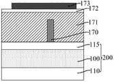
相应的,本发明实施例还提供一种半导体结构,包括:基底,包括用于形成目标图形的目标层;核心层,位于所述基底上且沿第一方向延伸,与所述第一方向相垂直的方向为第二方向;掩膜侧墙,位于所述核心层的侧壁上;第一分割层,沿第二方向延伸,所述第一分割层与所述掩膜侧墙沿第一方向的侧壁相接触;牺牲层,沿第一方向延伸、且沿第二方向与所述核心层间隔排列,所述牺牲层覆盖所述掩膜侧墙沿第一方向的侧壁,沿第一方向,所述牺牲层凸出于所述第一分割层的两侧且覆盖所述第一分割层的部分侧壁;平坦层,位于所述基底上且覆盖所述牺牲层、核心层、掩膜侧墙以及所述第一分割层的侧壁,所述平坦层露出所述牺牲层和核心层的顶面。Correspondingly, an embodiment of the present invention further provides a semiconductor structure, including: a substrate including a target layer for forming a target pattern; a core layer located on the substrate and extending along a first direction, which is opposite to the first direction The vertical direction is the second direction; the mask spacers are located on the side walls of the core layer; the first dividing layer extends along the second direction, and the first dividing layer and the mask spacers are along the first The sacrificial layer extends along the first direction and is spaced from the core layer along the second direction, the sacrificial layer covers the sidewall of the mask sidewall along the first direction, and the sacrificial layer covers the sidewall of the mask sidewall along the first direction, In one direction, the sacrificial layer protrudes from both sides of the first dividing layer and covers part of the sidewall of the first dividing layer; the flat layer is located on the substrate and covers the sacrificial layer, the core layer, The sidewalls and the sidewalls of the first dividing layer are masked, and the flat layer exposes the top surfaces of the sacrificial layer and the core layer.
与现有技术相比,本发明实施例的技术方案具有以下优点:Compared with the prior art, the technical solutions of the embodiments of the present invention have the following advantages:
本发明实施例提供的半导体结构的形成方法中,在形成所述核心层和掩膜侧墙之后,先形成沿第二方向延伸的第一分割层,所述第一分割层与所述掩膜侧墙沿第一方向的侧壁相接触,再形成牺牲层,沿第一方向所述牺牲层凸出于所述第一分割层的两侧且覆盖所述第一分割层的部分侧壁,从而使得位于所述第一分割层两侧的牺牲层被所述第一分割层分割,在去除所述牺牲层形成第一凹槽后,沿第一方向所述第一凹槽相应被所述第一分割层分割,从而有利于使得沿第一方向相邻的第一凹槽之间能够实现更小的距离,在图形化第一凹槽和第二凹槽下方的目标层形成目标图形后,相邻的目标图形在头对头(Head ToHead,HTH)的位置处也能够实现更小的距离,有利于提高目标图形的布局设计灵活度和自由度;而且,本发明实施例先形成第一分割层,再形成牺牲层,第一分割层相应定义第一凹槽的切割尺寸和位置,与直接通过刻蚀工艺实现第一凹槽的分割相比,本发明实施例有利于降低对第一凹槽进行分割的难度、增大切割第一凹槽的工艺窗口,还能够通过调整第一分割层的尺寸的方式,对第一凹槽在头对头位置处的尺寸进行精确控制,进而有利于提高目标图形的图形精度和图形质量。In the method for forming a semiconductor structure provided by the embodiment of the present invention, after the core layer and the mask spacer are formed, a first dividing layer extending along the second direction is formed first, and the first dividing layer and the mask are formed first. The sidewalls are in contact with the sidewalls along the first direction, and then a sacrificial layer is formed, and the sacrificial layer protrudes from both sides of the first dividing layer along the first direction and covers part of the sidewalls of the first dividing layer, Therefore, the sacrificial layers on both sides of the first dividing layer are divided by the first dividing layer. After the sacrificial layer is removed to form the first groove, the first groove is correspondingly divided by the first groove along the first direction. The first dividing layer is divided, so that a smaller distance can be achieved between the adjacent first grooves along the first direction. After patterning the target layer under the first groove and the second groove to form the target pattern , the adjacent target graphics can also achieve a smaller distance at the head-to-head (Head ToHead, HTH) position, which is conducive to improving the flexibility and freedom of the layout design of the target graphics; A sacrificial layer is formed by dividing the layer, and the first dividing layer correspondingly defines the cutting size and position of the first groove. Compared with directly realizing the dividing of the first groove through an etching process, the embodiment of the present invention is beneficial to reduce the impact on the first groove. The difficulty of dividing the grooves, increasing the process window for cutting the first grooves, and by adjusting the size of the first dividing layer, the size of the first grooves at the head-to-head position can be precisely controlled, which is beneficial to Improve the graphics accuracy and graphics quality of the target graphics.
此外,本发明实施例先形成核心层,再在核心层的侧壁上形成掩膜侧墙,掩膜侧墙为外侧墙(Outer Spacer);在去除核心层形成第二凹槽之后,沿第一方向相邻的第二凹槽之间的距离由核心层定义,与先形成凹槽、再在凹槽的侧壁上形成内侧墙相比,本发明实施例中,沿第一方向相邻第二凹槽之间的距离不是相邻核心层之间的距离与两倍内侧墙厚度之和,有利于使沿第一方向相邻的第二凹槽之间实现更小的距离,相应地,在图形化所述第一凹槽和第二凹槽下方的目标层形成目标图形后,相邻的目标图形在头对头(Head ToHead)的位置处能够实现更小的距离,有利于提高目标图形的布局设计灵活度和自由度,还有利于节约工艺成本。In addition, in the embodiment of the present invention, a core layer is formed first, and then a mask spacer is formed on the sidewall of the core layer, and the mask spacer is an outer spacer; after the core layer is removed to form the second groove, along the first The distance between the second grooves adjacent in one direction is defined by the core layer. Compared with forming the grooves first and then forming the inner walls on the sidewalls of the grooves, in the embodiment of the present invention, the adjacent grooves along the first direction The distance between the second grooves is not the sum of the distance between the adjacent core layers and twice the thickness of the inner wall, which is beneficial to realize a smaller distance between the adjacent second grooves along the first direction, correspondingly , after patterning the target layer under the first groove and the second groove to form a target pattern, the adjacent target patterns can achieve a smaller distance at the head to head (Head ToHead) position, which is conducive to improving the target pattern. The flexibility and freedom of graphic layout design are also beneficial to saving process costs.
附图说明Description of drawings
图1至图46是本发明半导体结构的形成方法一实施例中各步骤对应的结构示意图。1 to 46 are schematic structural diagrams corresponding to each step in an embodiment of a method for forming a semiconductor structure of the present invention.
具体实施方式Detailed ways
由背景技术可知,如何提高形成于晶圆上的图形与目标图形的匹配度成为了一种挑战。具体地,目前后段制程中,金属互连线的图形化工艺的难度大,工艺窗口小。As known from the background art, how to improve the matching degree between the pattern formed on the wafer and the target pattern has become a challenge. Specifically, in the current back-end process, the patterning process of metal interconnection lines is difficult and the process window is small.
例如:当互连图案的图形较为复杂时,光刻工艺所需要的光罩(Mask)的数量较多,不仅导致工艺成本过高,而且光罩的图案复杂,光罩的光学邻近修正处理也具有较高的难度,导致形成的互连线的图形精度和图形质量较差,甚至还易导致互连线在不需要连接的位置处发生短接(Bridge)的问题。For example: when the pattern of the interconnect pattern is complex, the number of masks required for the lithography process is large, which not only leads to high process cost, but also the pattern of the mask is complex, and the optical proximity correction processing of the mask is also It has high difficulty, resulting in poor pattern precision and pattern quality of the formed interconnection lines, and even easily leads to the problem of short-circuiting (Bridge) of the interconnection lines at positions that do not need to be connected.
一种方法利用伪互连线(Dummy lines),以增大光刻工艺的窗口、降低掩膜图案复杂度。在器件工作时,这些伪互连线处于浮接状态,也就是说,这些互连线不与外部电路或其他互连结构电连接。但是,这些浮接的伪互连线容易增大后段互连的寄生电容,导致形成的半导体结构的性能不佳。One method utilizes dummy lines to increase the window of the photolithography process and reduce the complexity of the mask pattern. When the device is in operation, these dummy interconnect lines are in a floating state, that is, these interconnect lines are not electrically connected to external circuits or other interconnect structures. However, these floating dummy interconnect lines tend to increase the parasitic capacitance of the back-end interconnects, resulting in poor performance of the formed semiconductor structure.
为了解决所述技术问题,本发明实施例提供的半导体结构的形成方法中,在形成所述核心层和掩膜侧墙之后,先形成沿第二方向延伸的第一分割层,所述第一分割层与所述掩膜侧墙沿第一方向的侧壁相接触,再形成牺牲层,沿第一方向所述牺牲层凸出于所述第一分割层的两侧且覆盖所述第一分割层的部分侧壁,从而使得位于所述第一分割层两侧的牺牲层被所述第一分割层分割,在去除所述牺牲层形成第一凹槽后,沿第一方向所述第一凹槽相应被所述第一分割层分割,从而有利于使得沿第一方向相邻的第一凹槽之间能够实现更小的距离,在图形化第一凹槽和第二凹槽下方的目标层形成目标图形后,相邻的目标图形在头对头的位置处也能够实现更小的距离,有利于提高目标图形的布局设计灵活度和自由度;而且,本发明实施例先形成第一分割层,再形成牺牲层,第一分割层相应定义第一凹槽的切割尺寸和位置,与直接通过刻蚀工艺实现第一凹槽的分割相比,本发明实施例有利于降低对第一凹槽进行分割的难度、增大切割第一凹槽的工艺窗口,还能够通过调整第一分割层的尺寸的方式,对第一凹槽在头对头位置处的尺寸进行精确控制,进而有利于提高目标图形的图形精度和图形质量。In order to solve the technical problem, in the method for forming a semiconductor structure provided by the embodiment of the present invention, after the core layer and the mask spacer are formed, a first dividing layer extending along the second direction is first formed, and the first dividing layer is formed. The dividing layer is in contact with the sidewalls of the mask spacers along the first direction, and then a sacrificial layer is formed. The sacrificial layer protrudes from both sides of the first dividing layer and covers the first dividing layer along the first direction. Part of the sidewall of the dividing layer, so that the sacrificial layers on both sides of the first dividing layer are divided by the first dividing layer, and after removing the sacrificial layer to form a first groove, the first A groove is correspondingly divided by the first dividing layer, so that a smaller distance can be achieved between adjacent first grooves along the first direction, below the patterned first grooves and the second grooves After the target layer is formed into the target graphics, the adjacent target graphics can also achieve a smaller distance at the head-to-head position, which is conducive to improving the flexibility and freedom of the layout design of the target graphics; A split layer is formed, and then a sacrificial layer is formed, and the first split layer defines the cutting size and position of the first groove accordingly. Difficulty in dividing a groove, increasing the process window for cutting the first groove, and by adjusting the size of the first dividing layer, the size of the first groove at the head-to-head position can be precisely controlled, thereby having It is beneficial to improve the graphic precision and graphic quality of the target graphic.
为使本发明实施例的上述目的、特征和优点能够更为明显易懂,下面结合附图对本发明的具体实施例做详细的说明。图1至图46是本发明半导体结构的形成方法一实施例中各步骤对应的结构示意图。In order to make the above objects, features and advantages of the embodiments of the present invention more clearly understood, specific embodiments of the present invention will be described in detail below with reference to the accompanying drawings. 1 to 46 are schematic structural diagrams corresponding to each step in an embodiment of a method for forming a semiconductor structure of the present invention.
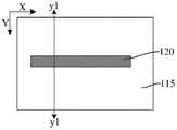
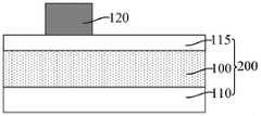
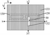
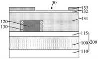
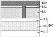
参考图1和图2,图2是图1沿y1-y1割线的剖面图,提供基底200,包括用于形成目标图形的目标层100。Referring to FIGS. 1 and 2, FIG. 2 is a cross-sectional view taken along the y1-y1 secant line of FIG. 1, providing a
基底200用于为后续工艺制程提供平台。目标层100为待进行图形化以形成目标图形的膜层。其中,目标图形可以为栅极结构、后段制程中的互连槽、鳍式场效应晶体管(FinFET)中的鳍部、全包围栅极(GAA)晶体管或叉型栅极晶体管(Forksheet)中的沟道叠层、硬掩膜(Hard Mask,HM)层等图形。The
本实施例中,目标层100为介电层。后续图形化介电层,在介电层中形成多个互连槽,之后再在互连槽中形成互连线,介电层用于实现相邻互连线之间的电隔离。相应地,本实施例中,所述目标图形为互连槽。因此,介电层为金属层间介质(Inter MetalDielectric,IMD)层。介电层的材料为低k介质材料、超低k介质材料、氧化硅、氮化硅或氮氧化硅等。In this embodiment, the
相应地,基底200中可以形成有晶体管、电容器等半导体器件,基底200 中还可以形成有电阻结构、导电结构等功能结构。本实施例中,基底200还包括位于目标层110底部的衬底110。作为一种示例,衬底110为硅衬底。Correspondingly, semiconductor devices such as transistors and capacitors can be formed in the
本实施例中,基底200还包括位于目标层100上的硬掩膜材料层115。后续先图形化硬掩膜材料层115形成硬掩膜层,再以硬掩膜层为掩膜图形化目标层100,有利于提高图形化目标层100的工艺稳定性和图形传递的精度。In this embodiment, the
硬掩膜材料层115的材料包括氮化钛、碳化钨、氧化硅、碳氧化硅和碳氮氧化硅中的一种或多种。作为一种示例,硬掩膜材料层115的材料为氮化钛。The material of the hard
在具体工艺中,根据实际的工艺需求,还能够在硬掩膜材料层115和目标层100之间设置应力缓冲层,以提高硬掩膜材料层115和目标层100之间的粘附性、减小膜层之间产生的应力。此外,还能够在硬掩膜材料层115和应力缓冲层之间、以及硬掩膜材料层115上设置刻蚀停止层,以定义后续刻蚀工艺的停止位置,有利于提高后续图形化工艺的效果。关于应力缓冲层和刻蚀停止层的相关描述,本实施例在此不再赘述。In the specific process, according to the actual process requirements, a stress buffer layer can also be arranged between the hard
继续参考图1和图2,在所述基底200上形成沿第一方向(如图1中X方向所示)延伸的核心层120,与所述第一方向相垂直的方向为第二方向(如图1 中Y方向所示)。Continuing to refer to FIG. 1 and FIG. 2 , a
核心层120用于为形成第二凹槽占据空间位置,从而定义后续第二凹槽的图形和位置。与直接通过刻蚀工艺形成第二凹槽相比,本实施例先形成核心层 120,后续再去除核心层120形成第二凹槽,从而通过调整核心层120的尺寸和形状,能够对第二凹槽的尺寸和形状进行精确控制,有利于降低第二凹槽的形成难度、使第二凹槽的图形精度得到保障,相应地,后续刻蚀第二凹槽下方的目标层100以形成目标图形后,有利于提高目标图形的图形精度。后续在核心层120的侧壁上形成掩膜侧墙,核心层120还为形成掩膜侧墙提供支撑。The
本实施例中,所述核心层120为易于被去除的材料,从而降低后续去除核心层120的难度。核心层120为单层或多层结构,核心层120的材料包括无定形硅、多晶硅、氧化硅、无定型碳、氮化硅、无定形锗、氮氧化硅、氮化碳、碳化硅、碳氮化硅和碳氮氧化硅中的一种或多种。作为一种示例,核心层120 为单层结构,核心层120的材料为无定形硅。In this embodiment, the
参考图3至图5,本实施例中,形成所述核心层120后,所述半导体结构的形成方法还包括:形成沿第二方向贯穿所述核心层120的切割槽20;沿第一方向所述核心层120被所述切割槽20分割。3 to 5 , in this embodiment, after the
切割槽20用于沿第一方向分割核心层120,从而使沿第一方向相邻核心层 120之间能够实现更小的距离,以使相邻的目标图形在头对头的位置处能够实现更小的距离。切割槽20还用于为形成第二分割层提供空间位置。The cutting
本实施例中,形成所述切割槽20的步骤包括以下步骤。In this embodiment, the step of forming the cutting
如图3所示,示出了在核心层120位置处沿第一方向的剖面图,在所述基底200上形成覆盖所述核心层120的图形层(未标示),包括自下而上依次堆叠的填充层121、第一抗反射涂层122以及第一光刻胶层123,所述第一光刻胶层 123中形成有第一图形开口10。所述图形层用于作为刻蚀核心层120的掩膜。As shown in FIG. 3 , a cross-sectional view along the first direction at the position of the
所述填充层121用于为形成第一抗反射涂层122和第一光刻胶层123提供平坦的表面。本实施例中,所述填充层121的材料为旋涂碳(SOC)。The
所述第一抗反射涂层122用于减小曝光时的反射效应,从而提高图形的转移精度。本实施例中,所述第一抗反射涂层为Si-ARC层,Si-ARC层有利于增加光刻工艺过程中的曝光景深(DOF),有利于提高曝光均匀性。在其他实施例中,第一抗反射涂层的材料还可以为BARC材料。The first
第一光刻胶层123用于作为刻蚀所述第一抗反射涂层122、填充层121以及核心层120的掩膜。光刻胶层123采用曝光、显影等光刻工艺形成。The
如图4和图5所示,图5为图4在核心层120位置处沿第一方向的剖面图,以第一光刻胶层123为掩膜,沿所述第一图形开口10,依次刻蚀所述第一抗反射涂层122、填充层121和所述核心层120,在所述核心层120中形成所述切割槽20;去除所述图形层。As shown in FIG. 4 and FIG. 5 , FIG. 5 is a cross-sectional view along the first direction at the position of the
本实施例中,采用各向异性的干法刻蚀工艺,依次刻蚀所述第一抗反射涂层122、填充层121和所述核心层120,。各向异性的干法刻蚀工艺具有各向异性刻蚀的特性,从而提高图形转移的精度。In this embodiment, an anisotropic dry etching process is used to sequentially etch the first
本实施例中,采用灰化工艺和湿法去胶工艺中的一种或两种,去除图形层。In this embodiment, one or both of an ashing process and a wet degumming process are used to remove the pattern layer.
在其他实施例中,形成所述核心层后,形成所述掩膜侧墙之前,所述半导体结构的形成方法还包括:对部分的所述核心层进行离子掺杂,适于提高所述核心层的耐刻蚀度,掺杂有离子的核心层用于作为第二分割层;沿第一方向所述核心层被所述第二分割层分割。离子掺杂适于提高耐核心层的耐刻蚀度,相应地,第二分割层的耐刻蚀度大于所述核心层的耐刻蚀度,相应提高核心层与第二分割层之间的刻蚀选择比,使得第二分割层能够在后续去除核心层以形成第二凹槽的过程中被保留,从而第二分割层能够分割第二凹槽。具体地,所述离子掺杂的离子包括硼离子、磷离子和氩离子中的一种或多种。In other embodiments, after the core layer is formed and before the mask spacer is formed, the method for forming the semiconductor structure further includes: performing ion doping on a part of the core layer, suitable for enhancing the core layer. The etching resistance of the layer, the core layer doped with ions is used as the second dividing layer; the core layer is divided by the second dividing layer along the first direction. Ion doping is suitable for improving the etching resistance of the core layer. Correspondingly, the etching resistance of the second split layer is greater than the etching resistance of the core layer, and the corrosion resistance between the core layer and the second split layer is correspondingly increased. The etching selectivity ratio is such that the second dividing layer can be retained during the subsequent removal of the core layer to form the second groove, so that the second dividing layer can divide the second groove. Specifically, the ion-doped ions include one or more of boron ions, phosphorus ions and argon ions.
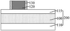
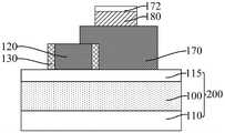
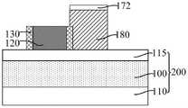
参考图6至图8,图7为图6沿y1-y1割线的剖面图,图8为图6在核心层120位置处沿第一方向的剖面图,在所述核心层120的侧壁上形成掩膜侧墙130。所述掩膜侧墙130用于作为后续图形化目标层100的掩膜。Referring to FIGS. 6 to 8 , FIG. 7 is a cross-sectional view along the y1-y1 secant line of FIG. 6 , and FIG. 8 is a cross-sectional view along the first direction at the position of the
后续形成第一凹槽和第二凹槽,所述掩膜侧墙130还用于隔离相邻的第一凹槽和第二凹槽,且本实施例还可以通过调整掩膜侧墙130的厚度,使后续第一凹槽和第二凹槽之间满足设计最小间隔。The first groove and the second groove are subsequently formed, and the
本实施例先形成核心层120,再在核心层120的侧壁上形成掩膜侧墙130,掩膜侧墙130为外侧墙(Outer Spacer);在去除核心层120形成第二凹槽之后,沿第一方向相邻的第二凹槽之间的距离由核心层120定义,与先形成凹槽、再在凹槽的侧壁上形成内侧墙相比,本实施例中,沿第一方向相邻第二凹槽之间的距离不是相邻核心层之间的距离与两倍内侧墙厚度之和,有利于使沿第一方向相邻的第二凹槽之间实现更小的距离,相应地,在图形化所述第一凹槽和第二凹槽下方的目标层形成目标图形后,相邻的目标图形在头对头(HeadTo Head)的位置处能够实现更小的距离,有利于提高目标图形的布局设计灵活度和自由度,还有利于节约工艺成本。In this embodiment, the
本实施例中,所述掩膜侧墙130填充于所述切割槽20,位于所述切割槽20 中的掩膜侧墙130用于作为第二分割层140,后续去除核心层120形成第二凹槽后,第二分割层140用于沿第一方向分割所述第二凹槽。In this embodiment, the
所述掩膜侧墙130选用与核心层120以及目标层100具有刻蚀选择性的材料,掩膜侧墙130的材料包括氧化钛、氧化硅、氮化硅、碳化硅、碳氧化硅、氧化铝和无定形硅中的一种或多种。The mask spacers 130 are selected from materials with etching selectivity to the
本实施例中,形成所述掩膜侧墙130的工艺包括原子层沉积工艺,有利于提高掩膜侧墙130的厚度均一性,并易于对掩膜侧墙130的厚度进行精确控制。In this embodiment, the process of forming the
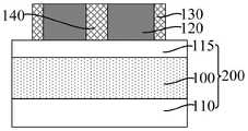
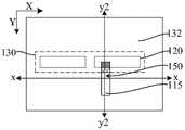
参考图9至图22,形成沿第二方向延伸的第一分割层170,所述第一分割层170与所述掩膜侧墙130沿第一方向的侧壁相接触。Referring to FIGS. 9 to 22 , a
所述第一分割层170用于沿第一方向分割后续的牺牲层,从而在后续去除牺牲层形成第一凹槽后,沿第一方向所述第一凹槽相应被所述第一分割层170 分割,有利于使得沿第一方向相邻的第一凹槽之间能够实现更小的距离,在图形化第一凹槽和第二凹槽下方的目标层100形成目标图形后,相邻的目标图形在头对头的位置处也能够实现更小的距离,有利于提高目标图形的布局设计灵活度和自由度,与直接通过刻蚀工艺实现第一凹槽的分割相比,本实施例有利于降低对第一凹槽进行分割的难度、增大切割第一凹槽的工艺窗口,还能够通过调整第一分割层170的尺寸的方式,对第一凹槽在头对头位置处的尺寸进行精确控制,进而有利于提高目标图形的图形精度和图形质量。The
本实施例中,沿第二方向,所述第一分割层170还延伸覆盖所述掩膜侧墙 130和核心层120的部分顶部,也就是说,所述第一分割层170为Overcut(过切割),从而不仅有利于降低对第一分割层170沿第二方向的尺寸精度的要求,而且还有利于防止出现第二分割层不能有效分割牺牲层的问题。In this embodiment, along the second direction, the
因此,所述第一分割层170选用与核心层120以及后续牺牲层具有刻蚀选择性的材料。本实施例中,所述第一分割层170的材料包括氧化硅、金属氧化物(例如:氧化钛)、多晶硅和无定型硅中的一种或多种。作为一种示例,所述第一分割层170的材料为氧化硅。Therefore, the
本实施例中,形成所述第一分割层170的步骤包括以下步骤。In this embodiment, the step of forming the
如图9至图11所示,图10为图9沿y2-y2割线的剖面图,图11为图9沿 x-x割线的剖面图,在所述核心层120和掩膜侧墙130露出的基底100上形成支撑层131。所述支撑层131用于后续形成切割开口,且在形成切割开口后,所述支撑层131用于为在切割开口中形成第一分割层提供支撑的作用。As shown in FIGS. 9 to 11 , FIG. 10 is a cross-sectional view along the y2-y2 secant line of FIG. 9 , and FIG. 11 is a cross-sectional view along the x-x secant line of FIG. 9 . The
后续形成第一分割层后,还会去除支撑层131,因此,支撑层131选用易于被去除的材料,以降低支撑层131的去除难度。本实施例中,支撑层131的材料为旋涂碳(Spin-OnCarbon,SOC)。旋涂碳适用于旋涂工艺,有利于降低形成支撑层131的难度、提高支撑层131的顶面平坦度,旋涂碳还易于被去除。After the first dividing layer is subsequently formed, the
在其他实施例中,所述支撑层的材料还可以包括有机介电层(OrganicDielectric layer,ODL)、底部抗反射涂层(Bottom Anti-reflective coating,BARC)、含硅抗反射层(Silicon Anti-reflective coating,Si-ARC)、深紫外光吸收氧化层 (DeepUV light absorbing Oxide,DUO)、介电抗反射涂层(Dielectric Anti-reflectiveCoating,DARC)和先进图膜(Advanced Patterning Film,APF) 中的一种或几种。相应地,本实施例中,采用旋涂工艺,形成所述支撑层131。In other embodiments, the material of the support layer may further include an organic dielectric layer (Organic Dielectric layer, ODL), a bottom anti-reflective coating (Bottom Anti-reflective coating, BARC), a silicon-containing anti-reflective layer (Silicon Anti-reflective layer) reflective coating, Si-ARC), deep UV light absorbing oxide (DeepUV light absorbing Oxide, DUO), dielectric anti-reflective coating (Dielectric Anti-reflective Coating, DARC) and advanced graphics film (Advanced Patterning Film, APF) of the one or more. Correspondingly, in this embodiment, a spin coating process is used to form the
本实施例中,在形成所述支撑层131后,所述形成方法还包括:在所述支撑层131上形成第二抗反射涂层132;在所述第二抗反射涂层132上形成第二光刻胶层133,所述第二光刻胶层133中形成有第二图形开口30。In this embodiment, after the supporting
第二光刻胶层133用于定义切割开口的尺寸和位置。第二抗反射涂层132 用于减小曝光时的反射效应。本实施例中,第二抗反射涂层132的材料为 BARC。The
如图12至图14所示,图13为图12沿y2-y2割线的剖面图,图14为图12沿x-x割线的剖面图,在支撑层131中形成沿第二方向延伸的切割开口150,所述切割开口150暴露出所述掩膜侧墙130沿第一方向的部分侧壁和部分的基底200。切割开口150用于定义第一分割层的尺寸和位置。As shown in FIGS. 12 to 14 , FIG. 13 is a cross-sectional view along the y2-y2 secant line of FIG. 12 , and FIG. 14 is a cross-sectional view along the x-x secant line of FIG. 12 , a cut extending along the second direction is formed in the
本实施例中,所述切割开口150还暴露出所述掩膜侧墙130和核心层120 的部分顶部及部分侧壁。本实施例中,形成所述切割开口150的步骤包括:以所述第二光刻胶层133为掩膜,沿所述第二图形开口30,依次刻蚀所述第二抗反射涂层132和支撑层131,在所述支撑层131中形成所述切割开口150。In this embodiment, the cutting
本实施例中,采用各向异性的干法刻蚀工艺,依次刻蚀所述第二抗反射涂层132和支撑层131,有利于提高图形传递的精度。本实施例中,刻蚀所述第二抗反射涂层132和支撑层131的步骤中,所述第二光刻胶层133被逐渐消耗,因此,在形成切割开口150后,所述第二光刻胶层133已经被去除。In this embodiment, an anisotropic dry etching process is used to sequentially etch the second
如图15至图19所示,在所述切割开口150中形成所述第一分割层170。As shown in FIGS. 15 to 19 , the
具体地,形成所述第一分割层170的步骤包括:如图15至图16所示,图 15为基于图13的剖面图,图16为基于图14的剖面图,在所述切割开口150 中形成分割材料层160,分割材料层160还覆盖于所述第二抗反射涂层132上;如图17至图19所示,图18为图17沿y2-y2割线的剖面图,图19为图17沿 x-x割线的剖面图,去除高于所述支撑层131的分割材料层160,剩余位于所述切割开口150中的分割材料层160用于作为第一分割层170。Specifically, the steps of forming the
形成所述第一分割层170的工艺包括旋涂工艺、原子层沉积工艺和化学气相沉积工艺中的一种或多种。本实施例中,采用旋涂工艺,形成分割材料层160。The process of forming the
本实施例中,采用刻蚀工艺(例如:各向异性的干法刻蚀工艺),去除高于所述支撑层131的分割材料层160。本实施例中,在去除高于所述支撑层131 的分割材料层160的步骤中,还去除所述第二抗反射涂层132。In this embodiment, an etching process (eg, anisotropic dry etching process) is used to remove the dividing
如图20至图22所示,图21为图20沿y2-y2割线的剖面图,图22为图 20沿x-x割线的剖面图,去除所述支撑层131。As shown in FIGS. 20 to 22, FIG. 21 is a cross-sectional view along the y2-y2 secant line of FIG. 20, and FIG. 22 is a cross-sectional view along the x-x secant line of FIG. 20, with the
去除所述支撑层131,以便于后续形成牺牲层。本实施例中,采用灰化工艺和湿法去胶工艺中的一种或两种,去除所述支撑层131。The
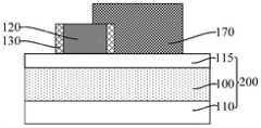
参考图23至图30,形成沿第一方向延伸、且沿第二方向与所述核心层120 间隔排列的牺牲层180,所述牺牲层180覆盖掩膜侧墙130沿第一方向的侧壁,沿第一方向,所述牺牲层180凸出于所述第一分割层170的两侧且覆盖所述第一分割层170的部分侧壁。Referring to FIGS. 23 to 30 , a
牺牲层180用于为形成第一凹槽占据空间,相应地,牺牲层180用于定义第一凹槽的图形和位置。与直接通过刻蚀工艺形成第一凹槽的方案相比,后续去除牺牲层180形成第一凹槽,有利于降低形成第一凹槽的难度,相应有利于使第一凹槽的图形精度得到保障。The
本实施例中,沿第一方向所述牺牲层180被第一分割层170分割,从而在去除牺牲层180形成第一凹槽后,沿第一方向所述第一凹槽相应被所述第一分割层170分割,有利于使得沿第一方向相邻的第一凹槽之间能够实现更小的距离,在图形化第一凹槽和第二凹槽下方的目标层100形成目标图形后,相邻的目标图形在头对头(HTH)的位置处也能够实现更小的距离。In this embodiment, the
本实施例中,通过先形成核心层120和位于核心层120侧壁的掩膜侧墙 130,再形成牺牲层180,相应地,牺牲层180与核心层120之间能够被掩膜侧墙130隔离,有利于使牺牲层180与核心层120之间满足设计最小间隔,相应使第二凹槽与第一凹槽之间满足设计最小间隔。In this embodiment, the
而且,本实施例分别在不同步骤中形成核心层120和牺牲层180,并通过核心层120和牺牲层180来定义第一凹槽和第二凹槽的图形,相应有利于降低形成第一凹槽、第二凹槽的难度,进而有利于提高第一凹槽和第二凹槽的图形精度,后续刻蚀第一凹槽和第二凹槽下方的目标层100以形成目标图形时,相应有利于使目标图形具有较高的图形精度。Moreover, in this embodiment, the
牺牲层180为单层或叠层结构,牺牲层180的材料包括旋涂碳、氧化硅、金属氧化物、有机介电层材料和先进图膜材料中的一种或多种。其中,氧化硅包括旋涂氧化硅(Spin-On-Glass,SOG);金属氧化物包括旋涂金属氧化物 (Spin-On Metal Oxide)。牺牲层180的材料适用于旋涂工艺,有利于降低形成牺牲层180的难度、提高牺牲层180的顶面平坦度。本实施例中,牺牲层140 的材料为旋涂碳。旋涂碳的填充性能较好,且旋涂碳材料易于被刻蚀,有利于降低形成牺牲层180的难度。The
本实施例中,形成所述牺牲层180的步骤中,所述牺牲层180还覆盖所述第一分割层170的部分顶部。In this embodiment, in the step of forming the
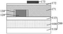
作为一种示例,形成牺牲层180的步骤包括以下步骤。As an example, the step of forming the
如图23至图26所示,图24为图23沿y2-y2割线的剖面图,图25为图 23沿y1-y1割线的剖面图,图26为图23沿x-x割线的剖面图,在基底200上形成覆盖核心层120的牺牲材料层171。为方便示意和说明,在图23中用虚线框示意出了核心层120、掩膜侧墙130和第一分割层170的形状和位置。As shown in FIGS. 23 to 26 , FIG. 24 is a cross-sectional view of FIG. 23 along the y2-y2 secant line, FIG. 25 is a cross-sectional view of FIG. 23 along the y1-y1 secant line, and FIG. 26 is a cross-sectional view of FIG. 23 along the x-x secant line In FIG. 2 , a
牺牲材料层171用于形成牺牲层。本实施例中,采用旋涂工艺形成牺牲材料层171。旋涂工艺操作简单、工艺成本低,且有利于提高牺牲材料层171的顶面平坦度,相应有利于提高后续图形化牺牲材料层171时的图形转移精度。The
本实施例中,所述形成方法还包括:在所述牺牲材料层171上形成第三抗反射涂层172、以及位于所述第三抗反射涂层172上的第三光刻胶层173。In this embodiment, the forming method further includes: forming a third
第三光刻胶层173用于定义牺牲层的尺寸和位置。The
第三抗反射涂层172用于减小曝光时的反射效应。The third
结合参考图27至图30,图28为图27沿y2-y2割线的剖面图,图29为图 27沿y1-y1割线的剖面图,图30为图27沿x-x割线的剖面图,图形化牺牲材料层171,保留与核心层120沿第一方向侧壁相邻的部分牺牲材料层171作为牺牲层180。27 to 30, FIG. 28 is a sectional view of FIG. 27 along the y2-y2 secant line, FIG. 29 is a sectional view of FIG. 27 along the y1-y1 secant line, and FIG. 30 is a sectional view of FIG. 27 along the x-x secant line , the
本实施例中,牺牲层180的顶面高于核心层120的顶面,从而省去了去除高于核心层120顶面的牺牲层180的步骤,有利于进一步简化工艺。In this embodiment, the top surface of the
本实施例中,以所述第三光刻胶层173为掩膜,依次刻蚀所述第三抗反射涂层172和牺牲材料层171,剩余的牺牲材料层171用于作为所述牺牲层180、In this embodiment, using the
本实施例中,采用各向异性的干法刻蚀工艺,依次刻蚀所述第三抗反射涂层172和牺牲材料层171,从而提高图形传递的精度。In this embodiment, an anisotropic dry etching process is used to sequentially etch the third
本实施例中,在刻蚀所述第三抗反射涂层172和牺牲材料层171的步骤中,所述第三光刻胶层173也逐渐被消耗,从而在形成牺牲层180后,所述第三光刻胶层173已经被去除。In this embodiment, in the step of etching the third
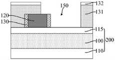
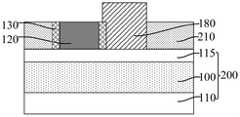
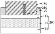
参考图31至图37,在所述牺牲层180、核心层120、掩膜侧墙130和第一分割层170露出的基底200上形成平坦层210。平坦层210用于与掩膜侧墙130、第一分割层170作为图形化目标层100的掩膜。Referring to FIGS. 31 to 37 , a
平坦层210选用与核心层120、牺牲层180的材料具有刻蚀选择性的材料。本实施例中,所述平坦层210的材料包括氧化硅、金属氧化物(例如:氧化钛)、多晶硅和无定型硅。作为一种示例,所述平坦层210的材料与第一分割层170 的材料相同,从而能够在形成平坦层210的过程中去除位于所述核心层120上的第一分割层170。相应地,平坦层210的材料为氧化硅。The
本实施例中,形成所述平坦层210的步骤包括以下步骤。In this embodiment, the step of forming the
如图31至图33所示,图31是基于图28的剖面图,图32是基于图29的剖面图,图33是基于图30的剖面图,在所述基底200上形成覆盖所述核心层 120、掩膜侧墙130、牺牲层180以及第一分割层170的平坦材料层190。31 to 33, FIG. 31 is a cross-sectional view based on FIG. 28, FIG. 32 is a cross-sectional view based on FIG. 29, and FIG. 33 is a cross-sectional view based on FIG. The
形成平坦材料层190的工艺包括原子层沉积工艺、化学气相沉积工艺和旋涂工艺中的一种或多种。作为一种示例,采用旋涂工艺形成平坦材料层190。旋涂工艺操作简单,工艺成本低,且有利于提高平坦材料层190的顶面平坦度。The process of forming the
如图34至图37所示,图35为图34沿y2-y2割线的剖面图,图36为图 34沿y1-y1割线的剖面图,图37为图34沿x-x割线的剖面图,回刻蚀所述平坦材料层190,暴露出所述牺牲层180。As shown in Figs. 34 to 37, Fig. 35 is a cross-sectional view of Fig. 34 along the y2-y2 secant line, Fig. 36 is a cross-sectional view of Fig. 34 along the y1-y1 secant line, and Fig. 37 is a cross-sectional view of Fig. 34 along the x-x secant line In the figure, the
暴露出所述牺牲层180,从而后续能够在同一步骤中刻蚀所述牺牲层180 露出的平坦材料层190和第一分割层170,进而能够暴露出核心层120的顶面。The
如图34至图37所示,刻蚀所述牺牲层180露出的部分厚度平坦材料层190 和第一分割层170,暴露出所述核心层120的顶面,剩余的平坦材料层190用于作为所述平坦层210。暴露出核心层120的顶面,以便于后续去除核心层120。As shown in FIG. 34 to FIG. 37 , the partial thickness
本实施例中,在同一步骤中,刻蚀牺牲层180露出的部分厚度平坦材料层 190和第一分割层170,从而不需额外进行去除位于核心层120上的第一分割层 170的步骤,有利于提高工艺整合度和兼容性,还有利于节约工艺成本。In this embodiment, in the same step, the partial thickness
本实施例中,刻蚀所述牺牲层180露出的部分厚度平坦材料层190和第一分割层170后,所述第一分割层170包括位于所述牺牲层180下方的第一部分 71(如图35所示)和露出于牺牲层180的第二部分72(如图35所示),所述第二部分72的顶面与核心层120、平坦层210和掩膜侧墙130的顶面相齐平。In this embodiment, after etching the part of the thickness
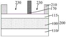
参考图38至图41,图39为图38沿y2-y2割线的剖面图,图40为图38 沿y1-y1割线的剖面图,图41为图38沿x-x割线的剖面图,去除所述牺牲层 180,在所述平坦层210中形成第一凹槽230,沿第一方向(如图38中x方向所示)所述第一凹槽230被所述第一分割层170分割。38 to 41, FIG. 39 is a cross-sectional view of FIG. 38 along the y2-y2 secant line, FIG. 40 is a cross-sectional view of FIG. 38 along the y1-y1 secant line, and FIG. 41 is a cross-sectional view of FIG. 38 along the x-x secant line, The
第一凹槽230用于定义部分目标图形的形状和位置。The
沿第一方向所述第一凹槽230被所述第一分割层170分割,有利于使得沿第一方向相邻的第一凹槽230之间能够实现更小的距离,在图形化第一凹槽230 和第二凹槽下方的目标层100形成目标图形后,相邻的目标图形在头对头的位置处也能够实现更小的距离,有利于提高目标图形的布局设计灵活度和自由度,与直接通过刻蚀工艺实现第一凹槽的分割相比,本实施例有利于降低对第一凹槽230进行分割的难度、增大切割第一凹槽230的工艺窗口,还能够通过调整第一分割层170的尺寸的方式,对第一凹槽230在头对头位置处的尺寸进行精确控制,进而有利于提高目标图形的图形精度和图形质量。The
本实施例中,去除所述牺牲层180的工艺对牺牲层180和第一分割层170 的刻蚀选择比高,因此第一分割层170的被误刻蚀概率低,从而防止第一凹槽 230在头对头的位置处的距离被增大,相应能够对第一凹槽230头对头位置处的距离进行精确控制。In this embodiment, the process of removing the
本实施例中,牺牲层180的材料为旋涂碳,采用灰化工艺和湿法去胶工艺中的一种或两种,去除所述牺牲层180。In this embodiment, the material of the
继续参考图38至图41,去除所述核心层120,在所述平坦层210中形成第二凹槽220。第二凹槽220和第一凹槽230用于定义目标图形的形状及位置。Continuing to refer to FIGS. 38 to 41 , the
本实施例中,沿第二方向,所述第一凹槽230和第二凹槽220之间被掩膜侧墙130隔离,有利于使第一凹槽230和第二凹槽220之间满足设计最小间隔。In this embodiment, along the second direction, the
本实施例中,掩膜侧墙130为外侧墙,在去除核心层120形成第二凹槽220 之后,沿第一方向相邻的第二凹槽220之间的距离由核心层120定义,与先形成凹槽、再在凹槽的侧壁上形成内侧墙相比,本实施例中,沿第一方向相邻第二凹槽之间的距离不是相邻核心层之间的距离与两倍内侧墙厚度之和,有利于使沿第一方向相邻的第二凹槽220之间实现更小的距离,相应地,在图形化所述第一凹槽230和第二凹槽220下方的目标层100形成目标图形后,相邻的目标图形在头对头的位置处能够实现更小的距离,有利于提高目标图形的布局设计灵活度和自由度,还有利于节约工艺成本。In this embodiment, the
本实施例中,去除核心层120的工艺包括湿法刻蚀和干法刻蚀中的一种或两种工艺。作为一种示例,采用湿法刻蚀工艺去除核心层120。本实施例中,湿法刻蚀工艺的刻蚀溶液包括TMAH溶液(四甲基氢氧化铵溶液),SC1溶液或SC2溶液。其中,SC1溶液指的是NH4OH和H2O2的混合溶液,SC2溶液指的是HCl和H2O2的混合溶液。In this embodiment, the process of removing the
本实施例中,去除所述核心层120后,沿第一方向所述第二凹槽220被所述第二分割层140分割,从而使相邻第二凹槽220之间实现更小的距离。In this embodiment, after the
参考图42至图45,图43为图42沿y2-y2割线的剖面图,图44为图42 沿y1-y1割线的剖面图,图45为图42沿x-x割线的剖面图,以所述掩膜侧墙 130、分割层170和平坦层210为掩膜,图形化所述第一凹槽230和第二凹槽 220下方的目标层100,形成目标图形300。42 to 45, FIG. 43 is a sectional view of FIG. 42 along the y2-y2 secant line, FIG. 44 is a sectional view of FIG. 42 along the y1-y1 secant line, and FIG. 45 is a sectional view of FIG. 42 along the x-x secant line, Using the
由前述可知,第一凹槽230和第二凹槽220在头对头的位置处均具有较小的距离,因此在刻蚀第一凹槽230和第二凹槽220下方的目标层100形成目标图形300时,相邻的目标图形300在头对头的位置处也能够实现更小的距离,有利于提高目标图形300的布局设计灵活度和自由度;而且,沿第二方向,第一凹槽230和第二凹槽220之间易于满足设计最小间隔,进而使目标图形300 之间易于满足设计最小间隔;此外,第一凹槽230和第二凹槽220具有较高的图形精度,相应有利于使目标图形300具有较高的图形精度。As can be seen from the foregoing, the
本实施例中,目标层100为介电层,因此,以所述掩膜侧墙130、分割层 170和平坦层210为掩膜,图形化所述第一凹槽230和第二凹槽220下方的介电层,形成互连槽(Trench)310。相应地,目标图形300为互连槽310。互连槽310用于为形成互连线提供空间。In this embodiment, the
具体地,本实施例中,以所述掩膜侧墙130、分割层170和平坦层210为掩膜,图形化所述第一凹槽230和第二凹槽220下方的硬掩膜材料层115,形成硬掩膜层240;以硬掩膜层240为掩膜,图形化介电层,形成所述互连槽310。Specifically, in this embodiment, the
结合参考图46,本实施例中,所述半导体结构的形成方法还包括:在形成所述互连槽310后,在所述互连槽310中形成互连线320。Referring to FIG. 46 , in this embodiment, the method for forming the semiconductor structure further includes: after forming the
本实施例中,互连槽310在头对头的位置处能够实现较小的距离,互连线 320在头对头的位置处相应也能够实现较小的距离,从而有利于提高互连线320 在头对头的位置处的连线能力,还有利于提高互连线320的布局设计的自由度和灵活度;而且,相邻的互连槽310在沿第二方向上的间隔易于满足设计最小间隔,同时,互连槽310的图形精度较高,相应有利于使互连线320在第二方向上的间隔满足设计最小间隔、以及提高互连线320的图形精度,进而提高半导体结构的性能。In this embodiment, the interconnecting
互连线320用于实现半导体结构与外部电路或其他互连结构的电连接。本实施例中,互连线320的材料为铜。其他实施例中,互连线的材料还能够为钴、钨、铝等导电材料。本实施例中,在形成互连线320的步骤中,还去除平坦层 210、掩膜侧墙130、第一分割层170以及硬掩膜层240,为后续制程做准备。
相应的,本发明还提供一种半导体结构。参考图34至图37,图35为图34 沿y2-y2割线的剖面图,图36为图34沿y1-y1割线的剖面图,图37为图34 沿x-x割线的剖面图,示出了本发明半导体结构一实施例的结构示意图。Correspondingly, the present invention also provides a semiconductor structure. Referring to FIGS. 34 to 37, FIG. 35 is a cross-sectional view of FIG. 34 along the y2-y2 secant line, FIG. 36 is a cross-sectional view of FIG. 34 along the y1-y1 secant line, and FIG. 37 is a cross-sectional view of FIG. 34 along the x-x secant line, A schematic structural diagram of an embodiment of the semiconductor structure of the present invention is shown.
所述半导体结构包括:基底200,包括用于形成目标图形的目标层100;核心层120,位于所述基底200上且沿第一方向(如图34中X方向所示)延伸,与所述第一方向相垂直的方向为第二方向(如图34中Y方向所示);掩膜侧墙 130,位于所述核心层120的侧壁上;第一分割层170,沿第二方向延伸,所述第一分割层170与所述掩膜侧墙130沿第一方向的侧壁相接触;牺牲层180,沿第一方向延伸、且沿第二方向与所述核心层120间隔排列,所述牺牲层180覆盖所述掩膜侧墙130沿第一方向的侧壁,沿第一方向,所述牺牲层180凸出于所述第一分割层170的两侧且覆盖第一分割层170的部分侧壁;平坦层210,位于所述基底200上且覆盖所述牺牲层180、核心层120、掩膜侧墙130以及所述第一分割层170的侧壁,平坦层210露出牺牲层180和核心层120的顶面。The semiconductor structure includes: a
牺牲层180用于为形成第一凹槽占据空间位置。核心层120用于为形成第二凹槽占据空间位置。The
所述第一分割层170用于沿第一方向分割牺牲层180,从而在后续去除牺牲层180形成第一凹槽后,沿第一方向第一凹槽相应被第一分割层170分割,有利于使得沿第一方向相邻的第一凹槽之间能够实现更小的距离,在图形化第一凹槽和第二凹槽下方的目标层100形成目标图形后,相邻的目标图形在头对头(Head To Head,HTH)的位置处也能够实现更小的距离,有利于提高目标图形的布局设计灵活度和自由度,与直接通过刻蚀工艺实现第一凹槽的分割相比,本实施例有利于降低对第一凹槽进行分割的难度、增大切割第一凹槽的工艺窗口,还能够通过调整第一分割层170的尺寸的方式,对第一凹槽在头对头位置处的尺寸进行精确控制,进而有利于提高目标图形的图形精度和图形质量。The
此外,本实施例中,掩膜侧墙130位于所述核心层120的外侧壁上,掩膜侧墙130为外侧墙;在形成第二凹槽之后,沿第一方向相邻的第二凹槽之间的距离由核心层120定义,与先形成凹槽、再在凹槽的侧壁上形成内侧墙相比,本实施例中,沿第一方向相邻第二凹槽之间的距离不是相邻核心层之间的距离与两倍内侧墙厚度之和,有利于使沿第一方向相邻的第二凹槽之间实现更小的距离,相应地,在图形化所述第一凹槽和第二凹槽下方的目标层形成目标图形后,相邻的目标图形在头对头的位置处能够实现更小的距离,有利于提高目标图形的布局设计灵活度和自由度,还有利于节约工艺成本。In addition, in this embodiment, the
基底200用于为工艺制程提供平台。目标层100为待进行图形化以形成目标图形的膜层。其中,目标图形可以为栅极结构、后段制程中的互连槽、鳍式场效应晶体管(FinFET)中的鳍部、全包围栅极(GAA)晶体管或叉型栅极晶体管(Forksheet)中的沟道叠层、硬掩膜(Hard Mask,HM)层等图形。The
本实施例中,目标层100为介电层。后续图形化介电层,在介电层中形成多个互连槽,之后再在互连槽中形成互连线,介电层用于实现相邻互连线之间的电隔离。相应地,本实施例中,所述目标图形为互连槽。因此,介电层为金属层间介质(IMD)层。介电层的材料为低k介质材料、超低k介质材料、氧化硅、氮化硅或氮氧化硅等。In this embodiment, the
相应地,本实施例中,基底200中可以形成有晶体管、电容器等半导体器件,基底200中还可以形成有电阻结构、导电结构等功能结构。本实施例中,所述基底200还包括位于目标层110底部的衬底110。Correspondingly, in this embodiment, semiconductor devices such as transistors and capacitors may be formed in the
本实施例中,基底200还包括位于所述目标层100上的硬掩膜材料层115。后续先图形化硬掩膜材料层115形成硬掩膜层,之后再以硬掩膜层为掩膜,图形化所述目标层100,有利于提高图形化目标层100的工艺稳定性,相应提高图形传递的精度。硬掩膜材料层115的材料包括氮化钛、碳化钨、氧化硅、碳氧化硅和碳氮氧化硅中的一种或多种。In this embodiment, the
核心层120用于为形成第二凹槽占据空间位置,从而定义第二凹槽的图形和位置。核心层120还为形成掩膜侧墙130提供支撑。The
本实施例中,所述核心层120为易于被去除的材料,从而降低后续去除核心层120的难度。核心层120为单层或多层结构,核心层120的材料包括无定形硅、多晶硅、氧化硅、无定型碳、氮化硅、无定形锗、氮氧化硅、氮化碳、碳化硅、碳氮化硅和碳氮氧化硅中的一种或多种。作为一种示例,核心层120 为单层结构,核心层120的材料为无定形硅。In this embodiment, the
本实施例中,所述半导体结构还包括:第二分割层140,沿第二方向贯穿所述核心层120;沿第一方向所述核心层120被所述第二分割层140分割。In this embodiment, the semiconductor structure further includes: a
所述第二分割层140用于沿第一方向分割所述核心层120,从而使沿第一方向相邻核心层120之间能够实现更小的距离,以使相邻的目标图形在头对头的位置处能够实现更小的距离。The
作为一种示例,所述半导体结构还包括:切割槽20(如图4所示),沿第二方向贯穿所述核心层120;所述掩膜侧墙130填充于所述切割槽20,位于所述切割槽20中的所述掩膜侧墙130用于作为所述第二分割层140。相应地,本实施例中,所述第二分割层140的材料与掩膜侧墙130的材料相同。As an example, the semiconductor structure further includes: a cutting groove 20 (as shown in FIG. 4 ), penetrating the
在其他实施例中,所述第二分割层与所述核心层的材料相同,且所述第二分割层中掺杂有离子,所述离子适于使所述第二分割层的耐刻蚀度大于所述核心层的耐刻蚀度。离子掺杂适于于使所述第二分割层的耐刻蚀度大于所述核心层的耐刻蚀度,相应提高核心层与第二分割层之间的刻蚀选择比,使得第二分割层能够在去除核心层以形成第二凹槽的过程中被保留,从而第二分割层能够分割第二凹槽。具体地,所述离子掺杂的离子包括硼离子、磷离子和氩离子中的一种或多种。所述第二分割层与所述核心层的材料相同,包括无定形硅、多晶硅、氧化硅、无定型碳、氮化硅、无定形锗、氮氧化硅、氮化碳、碳化硅、碳氮化硅和碳氮氧化硅中的一种或几种;所述掺杂离子包括硼离子、磷离子和氩离子中的一种或多种。In other embodiments, the material of the second dividing layer is the same as that of the core layer, and the second dividing layer is doped with ions, and the ions are suitable for making the second dividing layer resistant to etching is greater than the etch resistance of the core layer. Ion doping is suitable for making the etching resistance of the second split layer greater than the etching resistance of the core layer, and correspondingly increasing the etching selectivity ratio between the core layer and the second split layer, so that the second split layer is The layer can be retained during removal of the core layer to form the second groove, so that the second dividing layer can divide the second groove. Specifically, the ion-doped ions include one or more of boron ions, phosphorus ions and argon ions. The material of the second dividing layer is the same as that of the core layer, including amorphous silicon, polysilicon, silicon oxide, amorphous carbon, silicon nitride, amorphous germanium, silicon oxynitride, carbon nitride, silicon carbide, carbon nitride One or more of silicon oxide and silicon oxycarbonitride; the doping ions include one or more of boron ions, phosphorus ions and argon ions.
所述掩膜侧墙130用于作为后续图形化目标层100的掩膜。The
在形成第一凹槽和第二凹槽后,所述掩膜侧墙130还用于隔离相邻的第一凹槽和第二凹槽,且本实施例还可以通过调整掩膜侧墙130的厚度,使后续第一凹槽和第二凹槽之间满足设计最小间隔。After the first groove and the second groove are formed, the
掩膜侧墙130选用与核心层120、牺牲层180以及目标层100具有刻蚀选择性的材料,掩膜侧墙130的材料包括氧化钛、氧化硅、氮化硅、碳化硅、碳氧化硅、氧化铝和无定形硅中的一种或多种。The mask spacers 130 are selected from materials with etching selectivity to the
所述第一分割层170用于沿第一方向分割牺牲层180,从而在后续去除牺牲层180形成第一凹槽后,沿第一方向所述第一凹槽相应被所述第一分割层170 分割,有利于使得沿第一方向相邻的第一凹槽之间能够实现更小的距离,在图形化第一凹槽和第二凹槽下方的目标层100形成目标图形后,相邻的目标图形在头对头的位置处也能够实现更小的距离,有利于提高目标图形的布局设计灵活度和自由度,与直接通过刻蚀工艺实现第一凹槽的分割相比,本实施例有利于降低对第一凹槽进行分割的难度、增大切割第一凹槽的工艺窗口,还能够通过调整第一分割层170的尺寸的方式,对第一凹槽在头对头位置处的尺寸进行精确控制,进而有利于提高目标图形的图形精度和图形质量。The
所述第一分割层170选用与核心层120以及牺牲层180具有刻蚀选择性的材料。本实施例中,所述第一分割层170的材料包括氧化硅、金属氧化物(例如:氧化钛)、多晶硅和无定型硅中的一种或多种。作为一种示例,所述第一分割层170的材料和平坦层210的材料相同,第一分割层170的材料为氧化硅。The
本实施例中,第一分割层170包括位于牺牲层180下方的第一部分71和露出于牺牲层180的第二部分72,第二部分72的顶面与核心层120、平坦层210 和掩膜侧墙130的顶面相齐平,第二部分72通过在形成平坦层210的步骤中,以牺牲层180为掩膜,刻蚀部分厚度的第一分割层170和平坦层210形成。In this embodiment, the
牺牲层180用于为形成第一凹槽占据空间,相应地,牺牲层180用于定义第一凹槽的图形和位置。与直接通过刻蚀工艺形成第一凹槽的方案相比,后续去除牺牲层180形成第一凹槽,有利于降低形成第一凹槽的难度,相应有利于使第一凹槽的图形精度得到保障。The
本实施例中,沿第一方向所述牺牲层180被第一分割层170分割,从而在去除牺牲层180形成第一凹槽后,沿第一方向所述第一凹槽相应被所述第一分割层170分割,有利于使得沿第一方向相邻的第一凹槽之间能够实现更小的距离,在图形化第一凹槽和第二凹槽下方的目标层100形成目标图形后,相邻的目标图形在头对头的位置处也能够实现更小的距离。In this embodiment, the
本实施例中,牺牲层180与核心层120之间被掩膜侧墙130隔离,有利于使牺牲层180与核心层120之间满足设计最小间隔,相应使第二凹槽与第一凹槽之间满足设计最小间隔。In this embodiment, the
牺牲层180为单层或叠层结构,牺牲层180的材料包括旋涂碳、氧化硅、金属氧化物、有机介电层材料和先进图膜材料中的一种或多种。其中,氧化硅包括旋涂氧化硅;金属氧化物包括旋涂金属氧化物。牺牲层180的材料适用于旋涂工艺,有利于降低形成牺牲层180的难度、提高牺牲层180的顶面平坦度。本实施例中,牺牲层140的材料为旋涂碳。旋涂碳的填充性能较好,且旋涂碳材料易于被刻蚀,有利于降低形成牺牲层180的难度。The
本实施例中,所述牺牲层180还覆盖所述第一分割层170的部分顶部。In this embodiment, the
平坦层210用于与掩膜侧墙130、第一分割层170作为图形化目标层100 的掩膜。平坦层210选用与核心层120、牺牲层180的材料具有刻蚀选择性的材料。本实施例中,所述平坦层210的材料包括氧化硅、金属氧化物(例如:氧化钛)、多晶硅和无定型硅。作为一种示例,所述平坦层210的材料与第一分割层170的材料相同,从而能够在形成平坦层210的过程中去除位于所述核心层120上的第一分割层170。相应地,平坦层210的材料为氧化硅。The
所述半导体结构可以采用前述实施例所述的形成方法所形成,也可以采用其他形成方法所形成。对本实施例所述半导体结构的具体描述,可参考前述实施例中的相应描述,本实施例在此不再赘述。The semiconductor structure may be formed by the formation method described in the foregoing embodiments, or may be formed by other formation methods. For the specific description of the semiconductor structure in this embodiment, reference may be made to the corresponding descriptions in the foregoing embodiments, which will not be repeated in this embodiment.
虽然本发明披露如上,但本发明并非限定于此。任何本领域技术人员,在不脱离本发明的精神和范围内,均可作各种更动与修改,因此本发明的保护范围应当以权利要求所限定的范围为准。Although the present invention is disclosed above, the present invention is not limited thereto. Any person skilled in the art can make various changes and modifications without departing from the spirit and scope of the present invention. Therefore, the protection scope of the present invention should be based on the scope defined by the claims.
Claims (20)
Translated fromChinesePriority Applications (2)
| Application Number | Priority Date | Filing Date | Title |
|---|---|---|---|
| CN202011094777.0ACN114373713B (en) | 2020-10-14 | 2020-10-14 | Semiconductor structure and forming method thereof |
| US17/218,785US11651964B2 (en) | 2020-10-14 | 2021-03-31 | Semiconductor structure and forming method thereof |
Applications Claiming Priority (1)
| Application Number | Priority Date | Filing Date | Title |
|---|---|---|---|
| CN202011094777.0ACN114373713B (en) | 2020-10-14 | 2020-10-14 | Semiconductor structure and forming method thereof |
Publications (2)
| Publication Number | Publication Date |
|---|---|
| CN114373713Atrue CN114373713A (en) | 2022-04-19 |
| CN114373713B CN114373713B (en) | 2025-07-22 |
Family
ID=81077856
Family Applications (1)
| Application Number | Title | Priority Date | Filing Date |
|---|---|---|---|
| CN202011094777.0AActiveCN114373713B (en) | 2020-10-14 | 2020-10-14 | Semiconductor structure and forming method thereof |
Country Status (2)
| Country | Link |
|---|---|
| US (1) | US11651964B2 (en) |
| CN (1) | CN114373713B (en) |
Families Citing this family (1)
| Publication number | Priority date | Publication date | Assignee | Title |
|---|---|---|---|---|
| CN117080054B (en)* | 2023-09-22 | 2023-12-15 | 深圳市新凯来技术有限公司 | Method for preparing semiconductor structure |
Citations (3)
| Publication number | Priority date | Publication date | Assignee | Title |
|---|---|---|---|---|
| US20180315601A1 (en)* | 2017-04-28 | 2018-11-01 | Taiwan Semiconductor Manufacturing Company, Ltd. | Patterning Method for Semiconductor Device and Structures Resulting Therefrom |
| CN111524855A (en)* | 2019-02-02 | 2020-08-11 | 中芯国际集成电路制造(上海)有限公司 | Semiconductor structure and forming method thereof |
| CN111668099A (en)* | 2019-03-07 | 2020-09-15 | 中芯国际集成电路制造(上海)有限公司 | Patterning method and semiconductor device formed by same |
Family Cites Families (13)
| Publication number | Priority date | Publication date | Assignee | Title |
|---|---|---|---|---|
| US9153478B2 (en)* | 2013-03-15 | 2015-10-06 | Taiwan Semiconductor Manufacturing Company, Ltd. | Spacer etching process for integrated circuit design |
| US10361286B2 (en)* | 2016-06-24 | 2019-07-23 | Taiwan Semiconductor Manufacturing Co., Ltd. | Method and structure for mandrel and spacer patterning |
| US10529617B2 (en)* | 2017-09-29 | 2020-01-07 | Taiwan Semiconductor Manufacturing Company, Ltd. | Metal routing with flexible space formed using self-aligned spacer patterning |
| US10692812B2 (en)* | 2018-05-15 | 2020-06-23 | Globalfoundries Inc. | Interconnects with variable space mandrel cuts formed by block patterning |
| US10490447B1 (en)* | 2018-05-25 | 2019-11-26 | International Business Machines Corporation | Airgap formation in BEOL interconnect structure using sidewall image transfer |
| US10192780B1 (en)* | 2018-05-29 | 2019-01-29 | Globalfoundries Inc. | Self-aligned multiple patterning processes using bi-layer mandrels and cuts formed with block masks |
| US11107728B2 (en)* | 2019-05-22 | 2021-08-31 | International Business Machines Corporation | Interconnects with tight pitch and reduced resistance |
| CN112151608B (en)* | 2019-06-28 | 2023-12-15 | 中芯国际集成电路制造(上海)有限公司 | Semiconductor structure and forming method thereof |
| CN112768344B (en)* | 2019-11-05 | 2023-07-04 | 中芯国际集成电路制造(上海)有限公司 | Semiconductor structure and forming method thereof |
| CN113782487B (en)* | 2020-06-10 | 2023-10-20 | 中芯国际集成电路制造(上海)有限公司 | Semiconductor structure and forming method thereof |
| CN113823591B (en)* | 2020-06-18 | 2023-06-06 | 中芯国际集成电路制造(上海)有限公司 | Semiconductor structure and forming method thereof |
| CN114373712B (en)* | 2020-10-14 | 2025-07-18 | 中芯国际集成电路制造(上海)有限公司 | Semiconductor structure and forming method thereof |
| CN114388430A (en)* | 2020-10-22 | 2022-04-22 | 中芯国际集成电路制造(上海)有限公司 | Method for forming semiconductor structure and mask |
- 2020
- 2020-10-14CNCN202011094777.0Apatent/CN114373713B/enactiveActive
- 2021
- 2021-03-31USUS17/218,785patent/US11651964B2/enactiveActive
Patent Citations (3)
| Publication number | Priority date | Publication date | Assignee | Title |
|---|---|---|---|---|
| US20180315601A1 (en)* | 2017-04-28 | 2018-11-01 | Taiwan Semiconductor Manufacturing Company, Ltd. | Patterning Method for Semiconductor Device and Structures Resulting Therefrom |
| CN111524855A (en)* | 2019-02-02 | 2020-08-11 | 中芯国际集成电路制造(上海)有限公司 | Semiconductor structure and forming method thereof |
| CN111668099A (en)* | 2019-03-07 | 2020-09-15 | 中芯国际集成电路制造(上海)有限公司 | Patterning method and semiconductor device formed by same |
Also Published As
| Publication number | Publication date |
|---|---|
| CN114373713B (en) | 2025-07-22 |
| US11651964B2 (en) | 2023-05-16 |
| US20220115234A1 (en) | 2022-04-14 |
Similar Documents
| Publication | Publication Date | Title |
|---|---|---|
| CN111524855B (en) | Semiconductor structure and forming method thereof | |
| CN109427651B (en) | Semiconductor structure and forming method thereof | |
| CN112151608B (en) | Semiconductor structure and forming method thereof | |
| CN113782487B (en) | Semiconductor structure and forming method thereof | |
| CN114373712B (en) | Semiconductor structure and forming method thereof | |
| CN114373713B (en) | Semiconductor structure and forming method thereof | |
| US11810787B2 (en) | Semiconductor structure formation method and mask | |
| CN114664727B (en) | Method for forming semiconductor structure | |
| US11309184B2 (en) | Semiconductor structure and formation method thereof | |
| CN114388431A (en) | Method for forming semiconductor structure | |
| CN113948462B (en) | Semiconductor structures and methods of forming them | |
| CN114639604A (en) | Method for forming semiconductor structure | |
| CN113948463B (en) | Semiconductor structure and forming method thereof | |
| CN113745151B (en) | Semiconductor structure and forming method thereof | |
| CN114171451B (en) | Semiconductor structure and method for forming the same | |
| CN113745152B (en) | Semiconductor structure and forming method thereof | |
| CN114823300B (en) | Method for forming semiconductor structure | |
| CN114823299B (en) | Method for forming semiconductor structure | |
| CN114639603B (en) | Method for forming semiconductor structure | |
| CN113782488B (en) | Semiconductor structure and forming method thereof | |
| CN113948461B (en) | Method for forming semiconductor structure | |
| CN114664728B (en) | Method for forming semiconductor structure | |
| CN115206936A (en) | Semiconductor structure and forming method thereof | |
| CN114823291A (en) | Method for forming semiconductor structure | |
| CN115223927A (en) | Method for forming semiconductor structure |
Legal Events
| Date | Code | Title | Description |
|---|---|---|---|
| PB01 | Publication | ||
| PB01 | Publication | ||
| SE01 | Entry into force of request for substantive examination | ||
| SE01 | Entry into force of request for substantive examination | ||
| GR01 | Patent grant | ||
| GR01 | Patent grant |