CN114343656A - Microneedle for nerve interface - Google Patents
Microneedle for nerve interfaceDownload PDFInfo
- Publication number
- CN114343656A CN114343656ACN202210023298.2ACN202210023298ACN114343656ACN 114343656 ACN114343656 ACN 114343656ACN 202210023298 ACN202210023298 ACN 202210023298ACN 114343656 ACN114343656 ACN 114343656A
- Authority
- CN
- China
- Prior art keywords
- microneedle
- electrode
- metal
- microneedle according
- electrode contact
- Prior art date
- Legal status (The legal status is an assumption and is not a legal conclusion. Google has not performed a legal analysis and makes no representation as to the accuracy of the status listed.)
- Pending
Links
Images


Landscapes
- Measurement And Recording Of Electrical Phenomena And Electrical Characteristics Of The Living Body (AREA)
Abstract
Translated fromChinese
Description
Translated fromChinese技术领域technical field
本发明属于神经接口技术领域,具体涉及一种用于神经接口的微针。The invention belongs to the technical field of neural interfaces, and in particular relates to a microneedle used for neural interfaces.
背景技术Background technique
在神经接口系统中,通过电极采集脑信号,其中电极包括侵入式和非侵入式等形式,侵入式电极采集的脑信号更为准确、可靠性更高。目前,侵入式微针结构多采用硅基材料,采用电镀或lift-off工艺在体电极上加工金属电极触点;这种金属电极触点不具备优秀的生物相容性,植入脑组织结构时容易导致结构性损伤,不利于长期稳体工作。In the neural interface system, brain signals are collected through electrodes, and the electrodes include invasive and non-invasive forms. The brain signals collected by invasive electrodes are more accurate and reliable. At present, invasive microneedle structures are mostly made of silicon-based materials, and metal electrode contacts are processed on the body electrode by electroplating or lift-off process; such metal electrode contacts do not have excellent biocompatibility, and when implanted into brain tissue structures It is easy to cause structural damage, which is not conducive to long-term stable work.
发明内容SUMMARY OF THE INVENTION
本发明涉及一种用于神经接口的微针及其制备方法,以及以该微针体与集成电路芯片集成连接形成的用于神经接口的微针和该微针结构的制备方法,至少可解决现有技术的部分缺陷。The present invention relates to a microneedle for neural interface and a preparation method thereof, as well as a microneedle for neural interface formed by integrally connecting the microneedle body and an integrated circuit chip and a preparation method of the microneedle structure, which can at least solve the problem of Some of the deficiencies of the prior art.
为解决前述问题,本实施例提供一种用于神经接口的微针,包括至少一个微针体,所述微针体包括至少一个体电极,所述体电极上设置有至少一个电极触点,所述电极触点由导电材料制作而成。In order to solve the aforementioned problems, the present embodiment provides a microneedle for a neural interface, comprising at least one microneedle body, the microneedle body comprising at least one body electrode, and at least one electrode contact is provided on the body electrode, The electrode contacts are made of conductive material.
进一步地,所述导电材料采用生物相容性材料制作而成。Further, the conductive material is made of biocompatible material.
进一步地,所述生物相容性材料包括石墨烯、Au、pt、Ti或合金。Further, the biocompatible material includes graphene, Au, pt, Ti or alloys.
进一步地,所述电极触点采用半导体工艺制作而成。Further, the electrode contacts are fabricated by a semiconductor process.
进一步地,所述半导体工艺包括干法转移方式或气相沉积法。Further, the semiconductor process includes a dry transfer method or a vapor deposition method.
进一步地,所述电极触点上涂覆有氧化铱或聚合物。Further, the electrode contacts are coated with iridium oxide or polymer.
进一步地,所述微针体的尾部具有至少一个焊点,所述焊点通过连接线与相应的所述电极触点连接。Further, the tail of the microneedle body has at least one solder joint, and the solder joint is connected to the corresponding electrode contact by a connecting wire.
进一步地,所述电极触点的形状呈圆形或多边形。Further, the shape of the electrode contact is a circle or a polygon.
进一步地,所述体电极上的所述电极触点呈错位或阵列排布。Further, the electrode contacts on the body electrode are arranged in a dislocation or array.
进一步地,所述体电极的宽度小于500微米。Further, the width of the body electrode is less than 500 microns.
本发明至少具有如下有益效果:本发明提供一种用于神经接口的微针,该微针包括至少一个微针体,所述微针体包括至少一个体电极,所述体电极上设置有至少一个电极触点,所述电极触点由导电材料制作而成。在体电极上设置有至少一个电极触点,可以采集更多的信号,进而提高空间分辨率和信号精确度。在体电极上设置有至少一个电极触点,可以采集更多的信号,进而提高空间分辨率和信号精确度。The present invention has at least the following beneficial effects: the present invention provides a microneedle for neural interface, the microneedle comprises at least one microneedle body, the microneedle body comprises at least one body electrode, and the body electrode is provided with at least one microneedle body. An electrode contact made of conductive material. At least one electrode contact is arranged on the body electrode, which can collect more signals, thereby improving spatial resolution and signal accuracy. At least one electrode contact is arranged on the body electrode, which can collect more signals, thereby improving spatial resolution and signal accuracy.
进一步地,相比于常规的硅基体电极,本发明采用石墨烯电极点,具有更好的生物相容性,可避免微针侵入时对脑组织结构等造成结构性损伤;采用石墨烯电极点也具有更高的机械强度和导电性,可相应地提高微针工作的可靠性。Further, compared with conventional silicon substrate electrodes, the present invention adopts graphene electrode points, which has better biocompatibility, and can avoid structural damage to brain tissue structure when the microneedle invades; the graphene electrode points are used. It also has higher mechanical strength and electrical conductivity, which can correspondingly improve the reliability of microneedle work.
附图说明Description of drawings
为了更清楚地说明本发明实施例或现有技术中的技术方案,下面将对实施例或现有技术描述中所需要使用的附图作简单地介绍,显而易见地,下面描述中的附图仅仅是本发明的一些实施例,对于本领域普通技术人员来讲,在不付出创造性劳动的前提下,还可以根据这些附图获得其它的附图。In order to illustrate the embodiments of the present invention or the technical solutions in the prior art more clearly, the following briefly introduces the accompanying drawings that are used in the description of the embodiments or the prior art. Obviously, the drawings in the following description are only These are some embodiments of the present invention, and for those of ordinary skill in the art, other drawings can also be obtained from these drawings without creative effort.
图1为本发明实施例提供的微针体的示意图;1 is a schematic diagram of a microneedle body provided in an embodiment of the present invention;
图2为本发明实施例提供的微针结构的示意图;2 is a schematic diagram of a microneedle structure provided in an embodiment of the present invention;
图3为本发明实施例提供的TSV互连方法的过程示意图。FIG. 3 is a schematic process diagram of a TSV interconnection method provided by an embodiment of the present invention.
具体实施方式Detailed ways
下面对本发明实施例中的技术方案进行清楚、完整地描述,显然,所描述的实施例仅仅是本发明一部分实施例,而不是全部的实施例。基于本发明中的实施例,本领域普通技术人员在没有做出创造性劳动前提下所获得的所有其它实施例,都属于本发明保护的范围。The technical solutions in the embodiments of the present invention will be described clearly and completely below. Obviously, the described embodiments are only a part of the embodiments of the present invention, rather than all the embodiments. Based on the embodiments of the present invention, all other embodiments obtained by those of ordinary skill in the art without creative efforts shall fall within the protection scope of the present invention.
实施例一:Example 1:
本实施例提供一种用于神经接口的微针,包括至少一个微针体,所述微针体包括至少一个体电极,所述体电极上设置有至少一个电极触点,所述电极触点由导电材料制作而成。This embodiment provides a microneedle for a neural interface, comprising at least one microneedle body, the microneedle body comprising at least one body electrode, and at least one electrode contact is provided on the body electrode, and the electrode contact Made of conductive material.
在具体应用场景下,所述导电材料采用生物相容性材料制作而成。其中,所述生物相容性材料包括石墨烯、Au、pt、Ti或合金。In a specific application scenario, the conductive material is made of a biocompatible material. Wherein, the biocompatible material includes graphene, Au, pt, Ti or alloy.
在本实施例中,所述电极触点采用半导体工艺制作而成。所述半导体工艺包括干法转移方式或气相沉积法。其中,气相沉积法包括化学气相沉积法和物理气相沉积法,采用物理气相沉积法沉积金属,采用化学气相沉积法沉积石墨烯。In this embodiment, the electrode contacts are fabricated by a semiconductor process. The semiconductor process includes a dry transfer method or a vapor deposition method. Among them, the vapor deposition method includes chemical vapor deposition method and physical vapor deposition method, the physical vapor deposition method is used to deposit metal, and the chemical vapor deposition method is used to deposit graphene.
在优选的实施例中,所述电极触点上涂覆有氧化铱或聚合物,以增加电极触点的阻抗,提高电极触点的载荷量,避免电荷流失。In a preferred embodiment, the electrode contacts are coated with iridium oxide or polymer to increase the resistance of the electrode contacts, increase the load capacity of the electrode contacts, and avoid charge loss.
在本实施例中,所述微针体的尾部具有至少一个焊点,所述焊点通过连接线与相应的所述电极触点连接。所述电极触点的形状呈圆形或多边形。其中,多边形包括四边形和六边形等,当电极触点采用石墨烯制作而成时,电极触点的形状呈六边形,当电极触点采用Au、pt、Ti或合金制作而成时,电极触点的形状呈四边形、六边形或圆形等。In this embodiment, the tail of the microneedle body has at least one solder joint, and the solder joint is connected to the corresponding electrode contact through a connecting wire. The shape of the electrode contact is circular or polygonal. Among them, polygons include quadrilaterals and hexagons, etc. When the electrode contacts are made of graphene, the shape of the electrode contacts is hexagonal, and when the electrode contacts are made of Au, pt, Ti or alloys, The shape of the electrode contacts is quadrilateral, hexagonal or circular.
在本实施例中,所述体电极上的所述电极触点呈错位或阵列排布。所述体电极的宽度小于500微米。In this embodiment, the electrode contacts on the body electrode are arranged in a dislocation or array. The width of the body electrode is less than 500 microns.
相比于常规的硅基体电极,本发明采用石墨烯电极点,具有更好的生物相容性,可避免微针侵入时对脑组织结构等造成结构性损伤;采用石墨烯电极点也具有更高的机械强度和导电性,可相应地提高微针工作的可靠性。Compared with conventional silicon substrate electrodes, the present invention adopts graphene electrode points, which has better biocompatibility, and can avoid structural damage to brain tissue structure when microneedles invade; the graphene electrode points also have better biocompatibility. High mechanical strength and electrical conductivity can correspondingly improve the reliability of microneedle work.
实施例二:Embodiment 2:
如图1,本发明实施例提供一种用于神经接口的微针,,包括至少一个微针体1,微针体1包括微针体的尾部11和形成于所述微针体的尾部11上的至少一个体电极12,所述体电极12设置有至少一个电极触点121,电极触点121采用生物相容性材料制作而成,所述生物相容性材料包括石墨烯、Au、pt、Ti或合金。As shown in FIG. 1, an embodiment of the present invention provides a microneedle for a neural interface, comprising at least one
在优选的实施例中,所述电极触点121采用石墨烯制作而成,所述电极触点上涂覆有氧化铱或聚合物,以提高电极触点的载荷量,避免电荷流失。In a preferred embodiment, the
在其中一个实施例中,如图1,上述微针体的尾部11为板状,各体电极12均设置于该微针体的尾部11的一个侧边上,各体电极12沿该侧边的长度方向依次排列;一般地,各体电极12采用均匀间隔排列方式。In one embodiment, as shown in FIG. 1 , the
一般地,体电极12上具有多个电极触点121,用于采集信号。各体电极12优选为采用相同规格,例如体电极12的形状、长度等均相同;各体电极12上的电极触点121数量及排布方式可相同,也可不同,一般采用相同的电极触点121数量及排布方式。可选地,上述体电极为硅基基体;和/或,上述微针体的尾部11为硅基微针体的尾部;优选为二者均采用硅基材料,并且体电极在微针体的尾部11上一体延伸而成。Generally, the
相比于常规的硅基体电极,采用石墨烯电极点具有更好的生物相容性,可避免微针侵入时对脑组织结构等造成结构性损伤;采用石墨烯电极点也具有更高的机械强度和导电性,可相应地提高微针工作的可靠性。Compared with conventional silicon-based electrodes, the use of graphene electrode points has better biocompatibility, which can avoid structural damage to the brain tissue structure when the microneedle invades; the use of graphene electrode points also has higher mechanical properties. Strength and conductivity, which can correspondingly improve the reliability of microneedle work.
在其中一个实施例中,上述石墨烯层为石墨烯薄膜。优选地,该石墨烯层采用如下方式形成:In one embodiment, the graphene layer is a graphene film. Preferably, the graphene layer is formed in the following manner:
先制备石墨烯薄膜,具体地:将金属箔片放入生产炉中,向生产炉中通入保护气体保护加热至800~1200℃,稳定温度并保持15~30min;然后停止通入保护气体,随之通入碳源气体,待反应完成后,切断电源,停止通入碳源气体;再通入保护气体排净碳源气体,在保护气体的环境下直至炉内冷却到室温,取出金属箔片,得到金属箔片上的石墨烯薄膜。First prepare the graphene film, specifically: put the metal foil into the production furnace, pass the protective gas into the production furnace to protect and heat to 800 ~ 1200 ℃, stabilize the temperature and keep it for 15 ~ 30min; then stop feeding the protective gas, Then, the carbon source gas is introduced. After the reaction is completed, the power supply is cut off, and the carbon source gas is stopped; then the protective gas is introduced to exhaust the carbon source gas, and the furnace is cooled to room temperature under the protective gas environment. sheet to obtain a graphene film on a metal foil.
石墨烯薄膜生长制作完成后,可通过干法转移等方式将石墨烯薄膜转移至体电极上。After the graphene film is grown and fabricated, the graphene film can be transferred to the bulk electrode by dry transfer or the like.
在另外的实施例中,在所述体电极上沉积石墨烯材料以形成所述石墨烯层。优选地,采用如下方式沉积形成石墨烯层。In further embodiments, a graphene material is deposited on the body electrode to form the graphene layer. Preferably, the graphene layer is formed by deposition in the following manner.
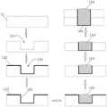
进一步优化上述微针体1的结构,如图1,所述微针体的尾部11上形成有多个连接通孔100,各所述连接通孔100均采用导电金属填充;所述体电极内设有电连接线并且对应的各电极触点121均与该电连接线连接,所述电连接线与部分连接通孔100内的导电金属连接。优选地,上述连接通孔100是采用TSV(Through-Silicon-Via,硅通孔)工艺形成的,作为优选方案,上述连接通孔100制作及导电金属的填充方式具体包括如下步骤:The structure of the
(1)如图3,在微针体的尾部11的一侧表面上刻蚀成槽101,其中,可以理解地,槽深方向平行于该构件的厚度方向;在其中一个实施例中,在微针体的尾部11上涂上光刻胶后,通过DRIE工艺(即深硅刻蚀工艺)刻蚀形成具有一定深度的槽101,显然地,该槽101的槽深小于微针体的尾部11的厚度;(1) As shown in Fig. 3, a
(2)如图3,在微针体的尾部11的成槽侧表面上沉积金属薄膜以作为电镀种子层102;金属薄膜的沉积方法为本领域常规技术,此处从略;(2) As shown in Fig. 3, a metal film is deposited on the grooved side surface of the
(3)在微针体的尾部11的成槽侧表面上电镀导电金属,在成槽处形成金属柱104,所述金属柱104的顶端凸出于槽外。其中,电镀导电金属可以采用常规的电镀金属操作,此处不作详述;可以理解地,上述金属柱104自槽底向槽外延伸,其可少量地凸出于槽外;优选地,在电镀操作之前,在成槽侧表面涂光刻胶103显影,使槽内的金属薄膜显露,以保证电镀精准性;(3) Electroplating conductive metal on the groove-forming side surface of the
(4)去除所述金属柱104以外的金属层;可选地,金属层采用湿法腐蚀方法去除;(4) removing the metal layers other than the
(5)将微针体的尾部11的另一侧表面减薄处理,以显露所述金属柱104的底端;减薄处理可以采用抛光等方式。(5) Thinning the surface of the other side of the
由此,即形成了上述的连接通孔100并且在该连接通孔100内填充有导电金属,该连接通孔100的结构及导电金属与该连接通孔100的结合结构也在上述方法中被限定清楚了(例如,上述导电金属包括附着在连接通孔100壁面上的电镀种子层102以及电镀形成在电镀种子层102上的电镀主体)。Thus, the above-mentioned connection via 100 is formed and filled with conductive metal. The structure of the connection via 100 and the combination structure of the conductive metal and the connection via 100 are also determined in the above method. The definition is clear (eg, the conductive metal described above includes a
在其中一个实施例中,上述导电金属为铜;优选地,采用钛作为电镀种子层102,其可起到黏附作用,使导电金属更好地附着在对应的结构上。当然,并不限于采用铜作为导电金属,其他的可导电金属也适用。In one of the embodiments, the above-mentioned conductive metal is copper; preferably, titanium is used as the
由于金属柱104的顶端凸出于槽外,当两个连接通孔100对接时,其中一通孔的金属柱104顶端与另一通孔的金属柱104底端抵接,可避免两个构件贴合连接时因构件间的间隙而导致金属柱104不能可靠接触的情况,因此能保证微针体的尾部11与其它构件之间的电连接可靠性。在其中一个实施例中,如图3,上述金属柱104的顶端呈曲面状,该形状的金属柱104易于电镀成型,同时在于其他金属柱104抵接时易于挤压抵紧。Since the top of the
进一步优选地,如图1和图2,所述微针体的尾部11上的各连接通孔100阵列分布,其中,通孔阵列的行向平行于所述体电极12的长度方向,通孔阵列的列向平行于各体电极12的排列方向,通孔阵列中的行数与体电极12数量相同并且一一对应配置,每行连接通孔100均与对应体电极12的电连接线连接。其中,优选地,在每个体电极12的根部延长线经过一行连接通孔100。基于上述结构,可保证微针体的尾部11与体电极12连接的可靠性,进而保证信号传输的准确性和可靠性。Further preferably, as shown in FIG. 1 and FIG. 2 , each connecting through
本实施例中,通过在微针体的尾部11上采用TSV工艺制作连接通孔100,适于与其他构件以TSV互连技术进行电性连接,可以实现信号的输入和输出,相应地优化神经接口系统的功能性,更好地满足临床需求。In this embodiment, by using the TSV process to make the connection through
实施例三:Embodiment three:
本发明实施例提供上述实施例一中的用于神经接口的微针的制备方法,包括:An embodiment of the present invention provides the method for preparing a microneedle for a neural interface in the above-mentioned first embodiment, including:
制备微针体的尾部11与体电极12的组合结构,其中,在体电极的表面预留多个电极触点121;Prepare a combined structure of the
在对应体电极12的体电极上形成石墨烯层。A graphene layer is formed on the body electrode corresponding to the
对于石墨烯薄膜式的石墨烯层以及沉积石墨烯层的形成方法,在上述实施例一中已有述及,此处不作赘述。The graphene film type graphene layer and the method for forming the deposited graphene layer have been described in the above-mentioned
实施例四:Embodiment 4:
如图2,本发明实施例提供一种用于神经接口的微针,包括微针体1和集成电路芯片2,所述微针体1采用上述实施例一所提供的用于神经接口的微针,所述集成电路芯片2与所述微针体的尾部11集成连接。As shown in FIG. 2 , an embodiment of the present invention provides a microneedle for a neural interface, including a
其中,上述微针体1优选为采用“微针体的尾部11上形成有多个连接通孔100,各连接通孔100均采用导电金属填充”的结构;上述集成电路芯片2上也优选为采用TSV工艺形成填充有导电金属的连接通孔100;微针体1的微针体的尾部11与集成电路芯片2贴合固定,二者的连接通孔100数量相同并且一一正对连通。Wherein, the above-mentioned
集成电路芯片2上的“填充有导电金属的连接通孔100”的制作方式可参考微针体1上的相关方案,此处不作赘述。For the manufacturing method of the "connecting through
在其中一个实施例中,上述集成电路芯片2为板状或块状构件,其可与板状微针体的尾部11采用面贴合的方式贴合固定。本实施例中,上述集成电路芯片2采用CMOS(Complementary Metal Oxide Semiconductor,互补金属氧化物半导体)电路单元,其具有成本低、集成度高、功耗低、兼容性高等特点,可实现信号的输入和输出,便于脑信号的采集和向神经接口系统的信号输送(包括其可将采集的脑信号进行筛选、放大等处理);特别地,上述CMOS电路单元采用硅基电路结构,适于与上述硅基微针体的尾部11较好地结合固定。In one embodiment, the above-mentioned
在其中一个实施例中,所述微针体的尾部11与所述集成电路芯片2键合连接,尤其是对于硅基电路结构和硅基微针体的尾部11,操作方便,连接稳定性高。In one embodiment, the
可选地,所述集成电路芯片2上设有测试焊盘21,该测试焊盘21可采用测试pad等结构,这种测试焊盘21在CMOS电路单元中应用较广,此处不作赘述。Optionally, the
本实施例提供的微针结构,将微针体1与集成电路芯片2集成,可以实现信号的输入和输出,相应地优化神经接口系统的功能性,更好地满足临床需求;基于TSV互连技术实现微针体1与集成电路芯片2之间的电性连接,连接可靠性高,能提高信号采集和传输的准确性和可靠性,同时,微针体1和集成电路芯片2可以各自沿用成熟工艺制备,工艺兼容性高,能有效地降低制备成本。The microneedle structure provided in this embodiment integrates the
本发明实施例还提供上述用于神经接口的微针的制备方法,包括,The embodiment of the present invention also provides the above-mentioned preparation method of the microneedle used for the neural interface, including:
S1,提供微针体1和集成电路芯片2;S1, providing
S2,在所述微针体的尾部11和所述集成电路芯片2上分别制作连接通孔100,所述连接通孔100的制作方法包括:S2, forming connecting through
S21,在对应构件的一侧表面上刻蚀成槽101;S21, etching
S22,在对应构件的成槽侧表面上沉积金属薄膜以作为电镀种子层102;S22, depositing a metal film on the grooved side surface of the corresponding component to serve as the
S23,在对应构件的成槽侧表面上电镀导电金属,在成槽处形成金属柱104,所述金属柱104的顶端凸出于槽外;去除所述金属柱104以外的金属层;S23, electroplating conductive metal on the groove-forming side surface of the corresponding component, forming a
S24,将对应构件的另一侧表面减薄处理,以显露所述金属柱104的底端;S24, thinning the other side surface of the corresponding component to expose the bottom end of the
S3,将所述微针体的尾部11与所述集成电路芯片2贴合,使二者的各连接通孔100一一对位,正对的两连接通孔100中,其中一通孔的金属柱104顶端与另一通孔的金属柱104底端抵接;随后完成所述微针体的尾部11与所述集成电路芯片2的固连。S3, attach the
其中,连接通孔100的制作方法在上述实施例一中已有详细述及,相关内容此处从略。The manufacturing method of the connecting through
S3中,微针体的尾部11与集成电路芯片2之间优选为采用键合连接方式。In S3, the
另外,基于TSV互连技术的连接方案能较好地满足微针装置的扩展需求,使多个微针体1集成成为可能,提高信号采集准确性、全面性和有效性,利于临床应用。如图2,具体地:In addition, the connection scheme based on the TSV interconnection technology can better meet the expansion requirements of the microneedle device, make it possible to integrate
上述微针结构包括两个微针体1和一个集成电路芯片2,两微针体1分布集成电路芯片2的两侧,其中,每个微针体1与集成电路芯片2均采用上述的TSV互连技术进行电连接;The above-mentioned microneedle structure includes two
或者,该微针结构包括多个微针体1和多个集成电路芯片2,各微针体1与各集成电路芯片2交错层设,其中,每个微针体1与相邻的集成电路芯片2均采用上述的TSV互连技术进行电连接。Alternatively, the microneedle structure includes a plurality of
可以理解地,相比于常规的单排微针,本实施例提供的微针结构可形成微针阵列,有更多的电极触点121,收集的信号更全面、更准确,具有极高的可靠性。It can be understood that, compared with the conventional single-row microneedle, the microneedle structure provided in this embodiment can form a microneedle array with
以上所述仅为本发明的较佳实施例而已,并不用以限制本发明,凡在本发明的精神和原则之内,所作的任何修改、等同替换、改进等,均应包含在本发明的保护范围之内。The above descriptions are only preferred embodiments of the present invention, and are not intended to limit the present invention. Any modification, equivalent replacement, improvement, etc. made within the spirit and principle of the present invention shall be included in the scope of the present invention. within the scope of protection.
Claims (10)
Priority Applications (1)
| Application Number | Priority Date | Filing Date | Title |
|---|---|---|---|
| CN202210023298.2ACN114343656A (en) | 2022-01-10 | 2022-01-10 | Microneedle for nerve interface |
Applications Claiming Priority (1)
| Application Number | Priority Date | Filing Date | Title |
|---|---|---|---|
| CN202210023298.2ACN114343656A (en) | 2022-01-10 | 2022-01-10 | Microneedle for nerve interface |
Publications (1)
| Publication Number | Publication Date |
|---|---|
| CN114343656Atrue CN114343656A (en) | 2022-04-15 |
Family
ID=81108929
Family Applications (1)
| Application Number | Title | Priority Date | Filing Date |
|---|---|---|---|
| CN202210023298.2APendingCN114343656A (en) | 2022-01-10 | 2022-01-10 | Microneedle for nerve interface |
Country Status (1)
| Country | Link |
|---|---|
| CN (1) | CN114343656A (en) |
Citations (12)
| Publication number | Priority date | Publication date | Assignee | Title |
|---|---|---|---|---|
| US5388577A (en)* | 1990-06-08 | 1995-02-14 | Boston University | Electrode array microchip |
| US20070123765A1 (en)* | 2005-10-07 | 2007-05-31 | Hetke Jamille F | Modular multichannel microelectrode array and methods of making same |
| CN102024782A (en)* | 2010-10-12 | 2011-04-20 | 北京大学 | Three-dimensional vertical interconnecting structure and manufacturing method thereof |
| CN102270603A (en)* | 2011-08-11 | 2011-12-07 | 北京大学 | Manufacturing method of silicon through hole interconnect structure |
| CN102280440A (en)* | 2011-08-24 | 2011-12-14 | 北京大学 | Laminated packaging structure and manufacturing method thereof |
| CN104257352A (en)* | 2014-10-08 | 2015-01-07 | 东南大学 | Network-type MEMS neural micro probe and manufacture method thereof |
| CN104548335A (en)* | 2014-12-26 | 2015-04-29 | 武汉格林泰克科技有限公司 | Implantable flexible array electrode used for organism and preparation method of implantable flexible array electrode |
| CN105748065A (en)* | 2016-01-21 | 2016-07-13 | 天津工业大学 | Moisture-retention microneedle matrix array surface bioelectric electrode |
| US20180078193A1 (en)* | 2016-09-16 | 2018-03-22 | International Business Machines Corporation | Flexible neural probes |
| CN109350847A (en)* | 2018-11-29 | 2019-02-19 | 深圳先进技术研究院 | A functionalized implantable flexible electrode and its application |
| CN113057640A (en)* | 2021-03-15 | 2021-07-02 | 四川省人民医院 | Implanted microneedle electrode, preparation method and functional instrument chip system |
| CN113855034A (en)* | 2021-09-10 | 2021-12-31 | 北京大学 | Microneedle electrode and preparation method thereof |
- 2022
- 2022-01-10CNCN202210023298.2Apatent/CN114343656A/enactivePending
Patent Citations (13)
| Publication number | Priority date | Publication date | Assignee | Title |
|---|---|---|---|---|
| US5388577A (en)* | 1990-06-08 | 1995-02-14 | Boston University | Electrode array microchip |
| US20070123765A1 (en)* | 2005-10-07 | 2007-05-31 | Hetke Jamille F | Modular multichannel microelectrode array and methods of making same |
| CN101583309A (en)* | 2005-10-07 | 2009-11-18 | 神经连结科技公司 | Modular multichannel microelectrode array and methods of making same |
| CN102024782A (en)* | 2010-10-12 | 2011-04-20 | 北京大学 | Three-dimensional vertical interconnecting structure and manufacturing method thereof |
| CN102270603A (en)* | 2011-08-11 | 2011-12-07 | 北京大学 | Manufacturing method of silicon through hole interconnect structure |
| CN102280440A (en)* | 2011-08-24 | 2011-12-14 | 北京大学 | Laminated packaging structure and manufacturing method thereof |
| CN104257352A (en)* | 2014-10-08 | 2015-01-07 | 东南大学 | Network-type MEMS neural micro probe and manufacture method thereof |
| CN104548335A (en)* | 2014-12-26 | 2015-04-29 | 武汉格林泰克科技有限公司 | Implantable flexible array electrode used for organism and preparation method of implantable flexible array electrode |
| CN105748065A (en)* | 2016-01-21 | 2016-07-13 | 天津工业大学 | Moisture-retention microneedle matrix array surface bioelectric electrode |
| US20180078193A1 (en)* | 2016-09-16 | 2018-03-22 | International Business Machines Corporation | Flexible neural probes |
| CN109350847A (en)* | 2018-11-29 | 2019-02-19 | 深圳先进技术研究院 | A functionalized implantable flexible electrode and its application |
| CN113057640A (en)* | 2021-03-15 | 2021-07-02 | 四川省人民医院 | Implanted microneedle electrode, preparation method and functional instrument chip system |
| CN113855034A (en)* | 2021-09-10 | 2021-12-31 | 北京大学 | Microneedle electrode and preparation method thereof |
Similar Documents
| Publication | Publication Date | Title |
|---|---|---|
| CN114305433A (en) | Microneedle based on integrated circuit chip | |
| TW563231B (en) | Semiconductor device substrate and manufacturing method thereof and semiconductor package | |
| TWI223976B (en) | Land grid array fabrication using elastomer core and conducting metal shell or mesh | |
| TWI242249B (en) | Three-dimensional device fabrication method | |
| CN112631425B (en) | Microneedle array type brain-computer interface device and preparation method thereof | |
| EP1355352A3 (en) | Stacked semiconductor device and method of manufacturing thereof | |
| CN104681454B (en) | The packaging technology of device is locked for novel finger print | |
| JP2006509215A5 (en) | ||
| EP3353845A1 (en) | Body-mountable device with a common substrate for electronics and battery | |
| CN110400781B (en) | Three-dimensional integrated packaging adapter plate based on glass substrate and manufacturing method thereof | |
| JPH02181475A (en) | Solar cell and its manufacturing method | |
| TW201246413A (en) | Compliant interconnects in wafers | |
| CN115727981A (en) | Flexible tactile measurement sensor with leadless packaging pressure chip and its preparation method | |
| TW200411891A (en) | High density multi-chip module structure and manufacturing method thereof | |
| US8178416B2 (en) | Method for making an electrically conducting mechanical interconnection member | |
| CN110428973A (en) | A kind of 3D body micro-silicon capacitor based on MEMS technology, its production and application | |
| CN114343656A (en) | Microneedle for nerve interface | |
| CN100466381C (en) | Method for flexible interconnection with implantable devices | |
| JP2002050780A (en) | Solar cell and method of manufacturing the same | |
| CN114098740A (en) | a microneedle | |
| CN210272322U (en) | Three-dimensional integrated packaging adapter plate based on glass substrate | |
| CN109478556A (en) | Detector module, detector, imaging device, and method of manufacturing a detector module | |
| CN109534284B (en) | Method for thermocompression welding between microelectrodes and flexible cables | |
| CN209993594U (en) | Three-dimensional integrated packaging adapter plate based on ceramic substrate | |
| CN112071935B (en) | Three-dimensional integrated system based on solar energy and preparation method |
Legal Events
| Date | Code | Title | Description |
|---|---|---|---|
| PB01 | Publication | ||
| PB01 | Publication | ||
| SE01 | Entry into force of request for substantive examination | ||
| SE01 | Entry into force of request for substantive examination | ||
| RJ01 | Rejection of invention patent application after publication | Application publication date:20220415 | |
| RJ01 | Rejection of invention patent application after publication |