CN1143394C - Peeling method, thin film device transfer method and thin film device - Google Patents
Peeling method, thin film device transfer method and thin film deviceDownload PDFInfo
- Publication number
- CN1143394C CN1143394CCNB971911347ACN97191134ACN1143394CCN 1143394 CCN1143394 CCN 1143394CCN B971911347 ACNB971911347 ACN B971911347ACN 97191134 ACN97191134 ACN 97191134ACN 1143394 CCN1143394 CCN 1143394C
- Authority
- CN
- China
- Prior art keywords
- layer
- thin film
- substrate
- separation layer
- light
- Prior art date
- Legal status (The legal status is an assumption and is not a legal conclusion. Google has not performed a legal analysis and makes no representation as to the accuracy of the status listed.)
- Expired - Lifetime
Links
Images


Classifications
- H—ELECTRICITY
- H01—ELECTRIC ELEMENTS
- H01L—SEMICONDUCTOR DEVICES NOT COVERED BY CLASS H10
- H01L21/00—Processes or apparatus adapted for the manufacture or treatment of semiconductor or solid state devices or of parts thereof
- H01L21/70—Manufacture or treatment of devices consisting of a plurality of solid state components formed in or on a common substrate or of parts thereof; Manufacture of integrated circuit devices or of parts thereof
- H01L21/71—Manufacture of specific parts of devices defined in group H01L21/70
- H01L21/76—Making of isolation regions between components
- H01L21/762—Dielectric regions, e.g. EPIC dielectric isolation, LOCOS; Trench refilling techniques, SOI technology, use of channel stoppers
- H01L21/7624—Dielectric regions, e.g. EPIC dielectric isolation, LOCOS; Trench refilling techniques, SOI technology, use of channel stoppers using semiconductor on insulator [SOI] technology
- H01L21/76251—Dielectric regions, e.g. EPIC dielectric isolation, LOCOS; Trench refilling techniques, SOI technology, use of channel stoppers using semiconductor on insulator [SOI] technology using bonding techniques
- G—PHYSICS
- G02—OPTICS
- G02F—OPTICAL DEVICES OR ARRANGEMENTS FOR THE CONTROL OF LIGHT BY MODIFICATION OF THE OPTICAL PROPERTIES OF THE MEDIA OF THE ELEMENTS INVOLVED THEREIN; NON-LINEAR OPTICS; FREQUENCY-CHANGING OF LIGHT; OPTICAL LOGIC ELEMENTS; OPTICAL ANALOGUE/DIGITAL CONVERTERS
- G02F1/00—Devices or arrangements for the control of the intensity, colour, phase, polarisation or direction of light arriving from an independent light source, e.g. switching, gating or modulating; Non-linear optics
- G02F1/01—Devices or arrangements for the control of the intensity, colour, phase, polarisation or direction of light arriving from an independent light source, e.g. switching, gating or modulating; Non-linear optics for the control of the intensity, phase, polarisation or colour
- G02F1/13—Devices or arrangements for the control of the intensity, colour, phase, polarisation or direction of light arriving from an independent light source, e.g. switching, gating or modulating; Non-linear optics for the control of the intensity, phase, polarisation or colour based on liquid crystals, e.g. single liquid crystal display cells
- G02F1/133—Constructional arrangements; Operation of liquid crystal cells; Circuit arrangements
- G02F1/1333—Constructional arrangements; Manufacturing methods
- G02F1/1345—Conductors connecting electrodes to cell terminals
- G02F1/13454—Drivers integrated on the active matrix substrate
- G—PHYSICS
- G02—OPTICS
- G02F—OPTICAL DEVICES OR ARRANGEMENTS FOR THE CONTROL OF LIGHT BY MODIFICATION OF THE OPTICAL PROPERTIES OF THE MEDIA OF THE ELEMENTS INVOLVED THEREIN; NON-LINEAR OPTICS; FREQUENCY-CHANGING OF LIGHT; OPTICAL LOGIC ELEMENTS; OPTICAL ANALOGUE/DIGITAL CONVERTERS
- G02F1/00—Devices or arrangements for the control of the intensity, colour, phase, polarisation or direction of light arriving from an independent light source, e.g. switching, gating or modulating; Non-linear optics
- G02F1/01—Devices or arrangements for the control of the intensity, colour, phase, polarisation or direction of light arriving from an independent light source, e.g. switching, gating or modulating; Non-linear optics for the control of the intensity, phase, polarisation or colour
- G02F1/13—Devices or arrangements for the control of the intensity, colour, phase, polarisation or direction of light arriving from an independent light source, e.g. switching, gating or modulating; Non-linear optics for the control of the intensity, phase, polarisation or colour based on liquid crystals, e.g. single liquid crystal display cells
- G02F1/133—Constructional arrangements; Operation of liquid crystal cells; Circuit arrangements
- G02F1/136—Liquid crystal cells structurally associated with a semi-conducting layer or substrate, e.g. cells forming part of an integrated circuit
- G02F1/1362—Active matrix addressed cells
- G02F1/1368—Active matrix addressed cells in which the switching element is a three-electrode device
- H—ELECTRICITY
- H01—ELECTRIC ELEMENTS
- H01L—SEMICONDUCTOR DEVICES NOT COVERED BY CLASS H10
- H01L21/00—Processes or apparatus adapted for the manufacture or treatment of semiconductor or solid state devices or of parts thereof
- H01L21/67—Apparatus specially adapted for handling semiconductor or electric solid state devices during manufacture or treatment thereof; Apparatus specially adapted for handling wafers during manufacture or treatment of semiconductor or electric solid state devices or components ; Apparatus not specifically provided for elsewhere
- H01L21/683—Apparatus specially adapted for handling semiconductor or electric solid state devices during manufacture or treatment thereof; Apparatus specially adapted for handling wafers during manufacture or treatment of semiconductor or electric solid state devices or components ; Apparatus not specifically provided for elsewhere for supporting or gripping
- H01L21/6835—Apparatus specially adapted for handling semiconductor or electric solid state devices during manufacture or treatment thereof; Apparatus specially adapted for handling wafers during manufacture or treatment of semiconductor or electric solid state devices or components ; Apparatus not specifically provided for elsewhere for supporting or gripping using temporarily an auxiliary support
- H—ELECTRICITY
- H01—ELECTRIC ELEMENTS
- H01L—SEMICONDUCTOR DEVICES NOT COVERED BY CLASS H10
- H01L21/00—Processes or apparatus adapted for the manufacture or treatment of semiconductor or solid state devices or of parts thereof
- H01L21/70—Manufacture or treatment of devices consisting of a plurality of solid state components formed in or on a common substrate or of parts thereof; Manufacture of integrated circuit devices or of parts thereof
- H01L21/71—Manufacture of specific parts of devices defined in group H01L21/70
- H01L21/76—Making of isolation regions between components
- H01L21/762—Dielectric regions, e.g. EPIC dielectric isolation, LOCOS; Trench refilling techniques, SOI technology, use of channel stoppers
- H01L21/7624—Dielectric regions, e.g. EPIC dielectric isolation, LOCOS; Trench refilling techniques, SOI technology, use of channel stoppers using semiconductor on insulator [SOI] technology
- H01L21/76251—Dielectric regions, e.g. EPIC dielectric isolation, LOCOS; Trench refilling techniques, SOI technology, use of channel stoppers using semiconductor on insulator [SOI] technology using bonding techniques
- H01L21/76254—Dielectric regions, e.g. EPIC dielectric isolation, LOCOS; Trench refilling techniques, SOI technology, use of channel stoppers using semiconductor on insulator [SOI] technology using bonding techniques with separation/delamination along an ion implanted layer, e.g. Smart-cut, Unibond
- H—ELECTRICITY
- H01—ELECTRIC ELEMENTS
- H01L—SEMICONDUCTOR DEVICES NOT COVERED BY CLASS H10
- H01L21/00—Processes or apparatus adapted for the manufacture or treatment of semiconductor or solid state devices or of parts thereof
- H01L21/70—Manufacture or treatment of devices consisting of a plurality of solid state components formed in or on a common substrate or of parts thereof; Manufacture of integrated circuit devices or of parts thereof
- H01L21/71—Manufacture of specific parts of devices defined in group H01L21/70
- H01L21/76—Making of isolation regions between components
- H01L21/762—Dielectric regions, e.g. EPIC dielectric isolation, LOCOS; Trench refilling techniques, SOI technology, use of channel stoppers
- H01L21/7624—Dielectric regions, e.g. EPIC dielectric isolation, LOCOS; Trench refilling techniques, SOI technology, use of channel stoppers using semiconductor on insulator [SOI] technology
- H01L21/76251—Dielectric regions, e.g. EPIC dielectric isolation, LOCOS; Trench refilling techniques, SOI technology, use of channel stoppers using semiconductor on insulator [SOI] technology using bonding techniques
- H01L21/76259—Dielectric regions, e.g. EPIC dielectric isolation, LOCOS; Trench refilling techniques, SOI technology, use of channel stoppers using semiconductor on insulator [SOI] technology using bonding techniques with separation/delamination along a porous layer
- H—ELECTRICITY
- H10—SEMICONDUCTOR DEVICES; ELECTRIC SOLID-STATE DEVICES NOT OTHERWISE PROVIDED FOR
- H10D—INORGANIC ELECTRIC SEMICONDUCTOR DEVICES
- H10D86/00—Integrated devices formed in or on insulating or conducting substrates, e.g. formed in silicon-on-insulator [SOI] substrates or on stainless steel or glass substrates
- H10D86/01—Manufacture or treatment
- H10D86/021—Manufacture or treatment of multiple TFTs
- H10D86/0214—Manufacture or treatment of multiple TFTs using temporary substrates
- H—ELECTRICITY
- H10—SEMICONDUCTOR DEVICES; ELECTRIC SOLID-STATE DEVICES NOT OTHERWISE PROVIDED FOR
- H10D—INORGANIC ELECTRIC SEMICONDUCTOR DEVICES
- H10D86/00—Integrated devices formed in or on insulating or conducting substrates, e.g. formed in silicon-on-insulator [SOI] substrates or on stainless steel or glass substrates
- H10D86/40—Integrated devices formed in or on insulating or conducting substrates, e.g. formed in silicon-on-insulator [SOI] substrates or on stainless steel or glass substrates characterised by multiple TFTs
- H10D86/60—Integrated devices formed in or on insulating or conducting substrates, e.g. formed in silicon-on-insulator [SOI] substrates or on stainless steel or glass substrates characterised by multiple TFTs wherein the TFTs are in active matrices
- G—PHYSICS
- G02—OPTICS
- G02F—OPTICAL DEVICES OR ARRANGEMENTS FOR THE CONTROL OF LIGHT BY MODIFICATION OF THE OPTICAL PROPERTIES OF THE MEDIA OF THE ELEMENTS INVOLVED THEREIN; NON-LINEAR OPTICS; FREQUENCY-CHANGING OF LIGHT; OPTICAL LOGIC ELEMENTS; OPTICAL ANALOGUE/DIGITAL CONVERTERS
- G02F1/00—Devices or arrangements for the control of the intensity, colour, phase, polarisation or direction of light arriving from an independent light source, e.g. switching, gating or modulating; Non-linear optics
- G02F1/01—Devices or arrangements for the control of the intensity, colour, phase, polarisation or direction of light arriving from an independent light source, e.g. switching, gating or modulating; Non-linear optics for the control of the intensity, phase, polarisation or colour
- G02F1/13—Devices or arrangements for the control of the intensity, colour, phase, polarisation or direction of light arriving from an independent light source, e.g. switching, gating or modulating; Non-linear optics for the control of the intensity, phase, polarisation or colour based on liquid crystals, e.g. single liquid crystal display cells
- G02F1/133—Constructional arrangements; Operation of liquid crystal cells; Circuit arrangements
- G02F1/136—Liquid crystal cells structurally associated with a semi-conducting layer or substrate, e.g. cells forming part of an integrated circuit
- G02F1/13613—Liquid crystal cells structurally associated with a semi-conducting layer or substrate, e.g. cells forming part of an integrated circuit the semiconductor element being formed on a first substrate and thereafter transferred to the final cell substrate
- H—ELECTRICITY
- H01—ELECTRIC ELEMENTS
- H01L—SEMICONDUCTOR DEVICES NOT COVERED BY CLASS H10
- H01L2221/00—Processes or apparatus adapted for the manufacture or treatment of semiconductor or solid state devices or of parts thereof covered by H01L21/00
- H01L2221/67—Apparatus for handling semiconductor or electric solid state devices during manufacture or treatment thereof; Apparatus for handling wafers during manufacture or treatment of semiconductor or electric solid state devices or components; Apparatus not specifically provided for elsewhere
- H01L2221/683—Apparatus for handling semiconductor or electric solid state devices during manufacture or treatment thereof; Apparatus for handling wafers during manufacture or treatment of semiconductor or electric solid state devices or components; Apparatus not specifically provided for elsewhere for supporting or gripping
- H01L2221/68304—Apparatus for handling semiconductor or electric solid state devices during manufacture or treatment thereof; Apparatus for handling wafers during manufacture or treatment of semiconductor or electric solid state devices or components; Apparatus not specifically provided for elsewhere for supporting or gripping using temporarily an auxiliary support
- H01L2221/68359—Apparatus for handling semiconductor or electric solid state devices during manufacture or treatment thereof; Apparatus for handling wafers during manufacture or treatment of semiconductor or electric solid state devices or components; Apparatus not specifically provided for elsewhere for supporting or gripping using temporarily an auxiliary support used as a support during manufacture of interconnect decals or build up layers
- H—ELECTRICITY
- H01—ELECTRIC ELEMENTS
- H01L—SEMICONDUCTOR DEVICES NOT COVERED BY CLASS H10
- H01L2221/00—Processes or apparatus adapted for the manufacture or treatment of semiconductor or solid state devices or of parts thereof covered by H01L21/00
- H01L2221/67—Apparatus for handling semiconductor or electric solid state devices during manufacture or treatment thereof; Apparatus for handling wafers during manufacture or treatment of semiconductor or electric solid state devices or components; Apparatus not specifically provided for elsewhere
- H01L2221/683—Apparatus for handling semiconductor or electric solid state devices during manufacture or treatment thereof; Apparatus for handling wafers during manufacture or treatment of semiconductor or electric solid state devices or components; Apparatus not specifically provided for elsewhere for supporting or gripping
- H01L2221/68304—Apparatus for handling semiconductor or electric solid state devices during manufacture or treatment thereof; Apparatus for handling wafers during manufacture or treatment of semiconductor or electric solid state devices or components; Apparatus not specifically provided for elsewhere for supporting or gripping using temporarily an auxiliary support
- H01L2221/68363—Apparatus for handling semiconductor or electric solid state devices during manufacture or treatment thereof; Apparatus for handling wafers during manufacture or treatment of semiconductor or electric solid state devices or components; Apparatus not specifically provided for elsewhere for supporting or gripping using temporarily an auxiliary support used in a transfer process involving transfer directly from an origin substrate to a target substrate without use of an intermediate handle substrate
- H—ELECTRICITY
- H10—SEMICONDUCTOR DEVICES; ELECTRIC SOLID-STATE DEVICES NOT OTHERWISE PROVIDED FOR
- H10D—INORGANIC ELECTRIC SEMICONDUCTOR DEVICES
- H10D30/00—Field-effect transistors [FET]
- H10D30/60—Insulated-gate field-effect transistors [IGFET]
- H10D30/67—Thin-film transistors [TFT]
- H10D30/6758—Thin-film transistors [TFT] characterised by the insulating substrates
Landscapes
- Physics & Mathematics (AREA)
- Engineering & Computer Science (AREA)
- General Physics & Mathematics (AREA)
- Microelectronics & Electronic Packaging (AREA)
- Condensed Matter Physics & Semiconductors (AREA)
- Manufacturing & Machinery (AREA)
- Computer Hardware Design (AREA)
- Power Engineering (AREA)
- Nonlinear Science (AREA)
- Mathematical Physics (AREA)
- Crystallography & Structural Chemistry (AREA)
- Chemical & Material Sciences (AREA)
- Optics & Photonics (AREA)
- Thin Film Transistor (AREA)
- Liquid Crystal (AREA)
- Electroluminescent Light Sources (AREA)
Abstract
Description
Translated fromChinese技术领域technical field
本发明涉及被剥离物的剥离方法,特别是涉及剥离由功能性薄膜那样的薄膜构成的被转移层并转移到透明基板那样的转移体上的转移方法。此外,本发明涉及薄膜器件的转移方法以及使用该方法制造的薄膜器件、薄膜集成电路装置和液晶显示装置。The present invention relates to a peeling method of a peeled object, and in particular to a transfer method of peeling a transferred layer made of a thin film such as a functional film and transferring it to a transfer body such as a transparent substrate. In addition, the present invention relates to a transfer method of a thin film device and a thin film device, a thin film integrated circuit device, and a liquid crystal display device manufactured by the method.
背景技术Background technique
例如在制造使用了薄膜晶体管(TFT)的液晶显示器时,经过用CVD法等在透明基板上形成薄膜晶体管的工序。For example, when a liquid crystal display using a thin film transistor (TFT) is manufactured, a process of forming a thin film transistor on a transparent substrate by a CVD method or the like is performed.
在该薄膜晶体管中,有使用非晶硅(a-Si)的薄膜晶体管和使用多晶硅(p-Si)的薄膜晶体管,再者,由多晶硅制成的薄膜晶体管可分类为经过高温工艺成膜的薄膜晶体管和经过低温工艺成膜的薄膜晶体管。Among the thin film transistors, there are thin film transistors using amorphous silicon (a-Si) and thin film transistors using polycrystalline silicon (p-Si). Furthermore, thin film transistors made of polysilicon can be classified as those formed by a high-temperature process. Thin film transistors and thin film transistors formed by a low-temperature process.
但是,由于以这种方式在透明基板上形成薄膜晶体管伴随较高的温度下的处理,因此必须使用耐热性优良的材料、即软化点和熔点高的材料作为透明基板。因此,现在在利用高温工艺制造TFT的情况下,使用由石英玻璃构成的透明性基板作为能充分地耐约1000℃的温度的基板。此外,在利用低温工艺制造TFT的情况下,由于500℃左右的温度为最高工艺温度,故使用能耐500℃左右的温度的耐热玻璃。However, since the formation of thin film transistors on a transparent substrate in this way involves high-temperature processing, it is necessary to use a material with excellent heat resistance, that is, a material with a high softening point and melting point, as the transparent substrate. Therefore, currently, when manufacturing TFTs by a high-temperature process, a transparent substrate made of quartz glass is used as a substrate that can sufficiently withstand a temperature of about 1000° C. In addition, in the case of manufacturing TFTs by a low-temperature process, since a temperature of about 500° C. is the highest process temperature, heat-resistant glass that can withstand a temperature of about 500° C. is used.
如上所述,安装薄膜器件的基板必须满足制造这些薄膜器件的条件。但是,如果只着眼于完成了安装薄膜器件的基板之后的阶段,则有时上述的「基板」不一定是比较理想的。As described above, substrates on which thin film devices are mounted must satisfy the conditions for manufacturing these thin film devices. However, if we only focus on the stage after the substrate on which the thin-film device is mounted, the above-mentioned "substrate" may not necessarily be ideal.
例如,在伴随高温处理的制造工艺中,使用石英玻璃或耐热玻璃,但与普通的玻璃相比,石英玻璃或耐热玻璃是稀少而且价格非常贵的材料,并且,制造大型的透明基板是困难的。For example, quartz glass or heat-resistant glass is used in a manufacturing process involving high-temperature treatment, but quartz glass or heat-resistant glass is a rare and very expensive material compared to ordinary glass, and manufacturing a large transparent substrate is difficult. difficult.
此外,石英玻璃也好,耐热玻璃也好,都是比较脆和容易破裂的,而且重量比较重。这一点在将形成了TFT那样的薄膜器件的基板安装在电子装置上的情况下成为很大的缺点。即,在起因于制造条件的制约和对制品所要求的较为理想的特性之间存在差距,要满足这些双方的条件或特性是极为困难的。In addition, whether it is quartz glass or heat-resistant glass, they are relatively brittle and easy to break, and they are relatively heavy. This point becomes a great disadvantage when mounting a substrate on which a thin-film device such as a TFT is formed on an electronic device. In other words, there is a gap between constraints due to manufacturing conditions and relatively ideal properties required for products, and it is extremely difficult to satisfy both of these conditions or properties.
发明内容Contents of the invention
本发明是着眼于这样的问题而完成的,其目的之一是提供一种不管被剥离物的特性、条件如何,可容易地剥离、特别是可转移到各种转移体上的剥离方法。此外,其目的在于提供一种可独立地自由地选择在薄膜器件的制造时使用的基板和例如在制品的实际使用时使用的基板(具有从制品的用途方面看较为理想的性质的基板)的新的技术。此外,其目的在于提供一种在该转移工艺中可使照射到产生剥离的分离层上的光能不降低、使转移到基板上的薄膜器件的特性不恶化的新的技术。The present invention has been made with such problems in mind, and one of its objects is to provide a peeling method that can be easily peeled, especially transferred to various transfer bodies, regardless of the characteristics and conditions of the object to be peeled. In addition, it is an object to provide a substrate that can independently and freely select a substrate used in the manufacture of a thin film device and a substrate used in the actual use of a product (a substrate having desirable properties from the viewpoint of the use of the product). new technology. In addition, the object is to provide a new technology that can prevent the light energy irradiated on the separation layer that causes peeling from being lowered and the characteristics of the thin-film device transferred on the substrate not to be deteriorated in the transfer process.
1.首先公开从制造基板剥离被剥离物或被转移层的剥离方法。这些发明如以下所述。1. First, a peeling method for peeling a peeled object or a transferred layer from a production substrate is disclosed. These inventions are as follows.
(1)本发明的剥离方法是一种将通过分离层存在于基板上的被剥离物从所述基板剥离的剥离方法,其特征在于:将照射光照射到所述分离层上,在所述分离层的层内和/或界面处使剥离产生,使所述被剥离物从所述基板脱离。(1) The peeling method of the present invention is a peeling method for peeling an object to be peeled that exists on a substrate through a separation layer from the substrate, and is characterized in that irradiation light is irradiated onto the separation layer, and in the The peeling occurs in the layer and/or at the interface of the separation layer, and the object to be peeled is detached from the substrate.
(2)一种将通过分离层存在于透光性的基板上的被剥离物从所述基板剥离的剥离方法,其特征在于:从所述基板一侧将照射光照射到所述分离层上,在所述分离层的层内和/或界面处使剥离产生,使所述被剥离物从所述基板脱离。(2) A peeling method for peeling an object to be peeled that exists on a light-transmitting substrate through a separation layer from the substrate, wherein irradiation light is irradiated onto the separation layer from the substrate side , causing peeling within the layer and/or at the interface of the separation layer, and detaching the object to be peeled from the substrate.
(3)一种将通过分离层形成于基板上的被转移层从所述基板剥离并转移到另一个转移体上的方法,其特征在于:在将所述转移体接合到所述被转移层的与所述基板相反的一侧之后,将照射光照射到所述分离层上,在所述分离层的层内和/或界面处使剥离产生,使所述被转移层从所述基板脱离并转移到所述转移体上。(3) A method of peeling and transferring a transferred layer formed on a substrate through a separation layer from the substrate to another transfer body, characterized in that: after bonding the transfer body to the transferred layer After the side opposite to the substrate, irradiation light is irradiated onto the separation layer to cause peeling within the layer and/or at the interface of the separation layer to detach the transferred layer from the substrate And transferred to the transfer body.
(4)一种将通过分离层形成于透光性的基板上的被转移层从所述基板剥离并转移到另一个转移体上的方法,其特征在于:在将所述转移体接合到所述被转移层的与所述基板相反的一侧之后,从所述基板一侧将照射光照射到所述分离层上,在所述分离层的层内和/或界面处使剥离产生,使所述被转移层从所述基板脱离并转移到所述转移体上。(4) A method of peeling a transferred layer formed on a light-transmitting substrate through a separation layer from the substrate and transferring it to another transfer body, wherein the transfer body is bonded to the transfer body. After removing the side of the transferred layer opposite to the substrate, irradiation light is irradiated onto the separation layer from the substrate side to cause peeling within the layer and/or at the interface of the separation layer, so that The transferred layer is detached from the substrate and transferred onto the transfer body.
(5)一种剥离方法,其特征在于,包括:在透光性的基板上形成分离层的工序;在所述分离层上直接地或通过规定的中间层形成被转移层的工序;将转移体接合到所述被转移层的与所述基板相反的一侧的工序;以及从所述基板一侧将照射光照射到所述分离层上,在所述分离层的层内和/或界面处使剥离产生,使所述被转移层从所述基板脱离并转移到所述转移体上的工序。(5) A peeling method, characterized in that it includes: a step of forming a separation layer on a light-transmitting substrate; a step of forming a transferred layer directly or through a predetermined intermediate layer on the separation layer; a process of body bonding to the side of the transferred layer opposite to the substrate; and irradiating irradiation light onto the separation layer from the substrate side, within layers and/or at the interface of the separation layer A step of causing peeling to detach the transferred layer from the substrate and transfer it to the transfer body.
此外,与以上的发明相关连,公开下述的发明。In addition, the following inventions are disclosed in connection with the above inventions.
可包括在将所述被转移层转移到所述转移体上之后,除去附着于所述基板一侧和/或所述转移体一侧的所述分离层的工序。A step of removing the separation layer adhering to the substrate side and/or the transfer body side after transferring the transferred layer onto the transfer body may be included.
此外,使用功能性薄膜或薄膜器件作为所述被转移层。特别是如果使用薄膜晶体管作为所述被转移层则是较为理想的。此外,将所述转移体定为透明基板是较为理想的。In addition, functional thin films or thin film devices are used as the transferred layer. It is ideal especially if a thin film transistor is used as the transferred layer. In addition, it is more desirable to set the transfer body as a transparent substrate.
再者,在将被转移层的形成时的最高温度设为Tmax时,用玻璃转变点(Tg)或软化点为Tmax以下的材料构成所述转移体是较为理想的。特别是用玻璃转变点(Tg)或软化点为800℃以下的材料构成所述转移体是较为理想的。Furthermore, when Tmax is the highest temperature at the time of forming the layer to be transferred, it is preferable to use a material having a glass transition point (Tg) or a softening point equal to or lower than Tmax. In particular, it is preferable to use a material having a glass transition point (Tg) or a softening point of 800° C. or lower to form the transfer body.
此外用合成树脂或玻璃材料构成所述转移体是较为理想的。In addition, it is desirable to form the transfer body from a synthetic resin or glass material.
此外,所述基板具有耐热性是较为理想的。特别是在将被转移层的形成时的最高温度设为Tmax时,用变形点为Tmax以上的材料构成所述基板是较为理想的。In addition, it is desirable that the substrate has heat resistance. In particular, when the maximum temperature at the time of forming the transferred layer is Tmax, it is preferable to form the substrate with a material having a deformation point equal to or higher than Tmax.
在以上的剥离方法中,借助于构成分离层的物质的原子间或分子间的结合力消失或减少来产生所述分离层的剥离。In the above peeling method, the peeling of the separation layer occurs by virtue of the disappearance or reduction of the bonding force between atoms or molecules of the substances constituting the separation layer.
此外,所述照射光是激光是较为理想的。特别是所述激光的波长是100~350nm是较为理想的。此外所述激光的波长是350~1200nm是较为理想的。In addition, it is preferable that the irradiation light is laser light. In particular, the wavelength of the laser light is preferably 100 to 350 nm. In addition, it is more ideal that the wavelength of the laser is 350-1200 nm.
再有,用非晶硅构成所述分离层是较为理想的。特别是所述非晶硅含有2at%以上的H(氢)是较为理想的。Furthermore, it is preferable to form the separation layer from amorphous silicon. In particular, it is desirable that the amorphous silicon contains H (hydrogen) at 2 at % or more.
此外,可用陶瓷构成所述分离层。也可用金属构成所述分离层。也可用有机高分子材料构成所述分离层。此时,所述有机高分子材料具有-CH2-、-CO-、-CONH-、-NH-、-COO-、-N=N-、-CH=N-中的至少一种结合是较为理想的。再者,所述有机高分子材料在构成式中具有芳香烃是较为理想的。In addition, ceramics may be used to constitute the separation layer. Metals can also be used to form the separation layer. The separation layer may also be constituted by an organic polymer material. At this time, the organic polymer material has at least one combination of -CH2 -, -CO-, -CONH-, -NH-, -COO-, -N=N-, -CH=N-. ideal. Furthermore, it is ideal that the organic polymer material has aromatic hydrocarbons in its constitutional formula.
2.其次,公开了由多个层叠体构成上述发明中的分离层的发明。这些发明如下所述。2. Next, an invention is disclosed in which the separation layer in the above invention is constituted by a plurality of laminates. These inventions are described below.
首先,其特征在于:由多层的层叠体构成前项1中公开的发明中的分离层。再者,其特征在于:所述分离层包含组成或特性不同的至少2层。First, it is characterized in that the separation layer in the invention disclosed in the
所述分离层包含吸收所述照射光的光吸收层和与该光吸收层组成或特性不同的另一层是较为理想的。特别是所述分离层包含吸收所述照射光的光吸收层和遮住所述照射光的遮光层是较为理想的。再者,所述遮光层相对于所述光吸收层位于与所述照射光的入射方向的相反一侧是较为理想的。再者,所述遮光层是反射所述照射光的反射层是较为理想的。特别是用金属薄膜构成所述反射层是较为理想的。The separation layer preferably includes a light-absorbing layer that absorbs the irradiated light and another layer having a different composition or characteristic from the light-absorbing layer. In particular, it is preferable that the separation layer includes a light absorbing layer that absorbs the irradiated light and a light shielding layer that blocks the irradiated light. Furthermore, it is desirable that the light-shielding layer is located on the opposite side to the incident direction of the irradiating light relative to the light-absorbing layer. Furthermore, it is preferable that the light-shielding layer is a reflective layer that reflects the irradiated light. In particular, it is preferable to form the reflective layer with a thin metal film.
3.其次,公开了将薄膜器件作为被剥离物或被转移体使用的薄膜器件的转移方法。3. Next, a transfer method of a thin film device using a thin film device as an object to be peeled or an object to be transferred is disclosed.
一种将基板上的薄膜器件转移到转移体上的方法,其特征在于包括:在所述基板上形成分离层的工序;在所述分离层上形成包含薄膜器件的被转移层的工序;通过粘接层将包含所述薄膜器件的被转移层接合到所述转移体上的工序;将光照射到所述分离层上,在所述分离层的层内和/或界面处使剥离产生的工序;以及使所述基板从所述分离层脱离的工序。A method for transferring a thin film device on a substrate to a transfer body, characterized by comprising: a step of forming a separation layer on the substrate; a step of forming a transferred layer containing the thin film device on the separation layer; The process of bonding the transferred layer including the thin film device to the transfer body by the adhesive layer; irradiating light onto the separation layer to cause peeling within the layer and/or at the interface of the separation layer a step; and a step of detaching the substrate from the separation layer.
按照本发明,在器件制造中的可靠性高的基板上预先设置具有吸收光的特性的分离层,在该基板上形成TFT等薄膜器件。其次,虽不作特别限定,但例如通过粘接层将薄膜器件接合到所希望的转移体上,其后将光照射到分离层上,由此在该分离层中使剥离现象产生,使该分离层与所述基板之间的密接性降低。然后,对基板加力,使该基板从薄膜器件脱离。由此,即使对什么样的转移体也能转移(形成)所希望的、可靠性高的器件。According to the present invention, a separation layer having light-absorbing properties is provided in advance on a substrate with high reliability in device manufacture, and thin-film devices such as TFTs are formed on the substrate. Secondly, although not particularly limited, for example, the thin film device is bonded to a desired transfer body through an adhesive layer, and light is then irradiated on the separation layer, thereby causing a peeling phenomenon in the separation layer and making the separation Adhesion between the layer and the substrate is lowered. Then, a force is applied to the substrate to release the substrate from the thin film device. Thus, a desired device with high reliability can be transferred (formed) to any transfer body.
再有,在本发明中,通过粘接层将薄膜器件(包含薄膜器件的被转移层)接合到转移体上的工序以及使基板从薄膜器件脱离的工序的顺序没有关系,哪个工序在前面都可以。但是,在使基板脱离之后的薄膜器件的操作方面有问题的情况下,希望首先将薄膜器件接合到转移体上,其后使基板脱离。Furthermore, in the present invention, the order of the step of bonding the thin film device (including the transferred layer of the thin film device) to the transfer body through the adhesive layer and the step of detaching the substrate from the thin film device does not matter, and whichever step comes first Can. However, if there is a problem with the handling of the thin-film device after detaching the substrate, it is desirable to first bond the thin-film device to the transfer body and then detach the substrate.
此外,如果使用例如具有平坦化作用的物质(例如热硬化性树脂)作为在将薄膜器件接合到转移体中使用的粘接层,则即使在包含薄膜器件的被转移层的表面上产生一些台阶,也能使该台阶平坦化而予以忽略,于是总是可以进行良好的向转移体的结合,是很方便的。再者,其特征在于:所述基板是透光性的基板,所述光向所述分离层的照射通过所述透光性的基板来进行。例如,如果使用石英基板等的透明基板,则在可制造可靠性高的薄膜器件的同时,也可使光从基板的背面一并照射分离层的整个面,可提高转移效率。In addition, if, for example, a substance having a flattening effect (such as a thermosetting resin) is used as the adhesive layer used in bonding the thin film device to the transfer body, even if some steps are generated on the surface of the transferred layer including the thin film device , the step can be flattened and ignored, so that good bonding to the transfer body can always be performed, which is very convenient. Furthermore, it is characterized in that the substrate is a translucent substrate, and the light is irradiated to the separation layer through the translucent substrate. For example, if a transparent substrate such as a quartz substrate is used, a highly reliable thin-film device can be manufactured, and light can also be irradiated to the entire surface of the separation layer from the back surface of the substrate, thereby improving transfer efficiency.
4.再者,公开了将上述第3项中公开了的薄膜器件的转移方法的工序的一部分进行了改良的发明。这些发明如下所述。4. Furthermore, it discloses an invention in which a part of the process of the method for transferring a thin film device disclosed in the
(1)一种将包含基板上的薄膜器件的被转移层转移到转移体上的方法,其特征在于,包括:在所述基板上形成非晶硅层的第1工序;在所述非晶硅层上形成包含所述薄膜器件的所述被转移层的第2工序;通过粘接层将包含所述薄膜器件的所述被转移层接合到所述转移体上的第3工序;通过所述基板将光照射到所述非晶硅层上,在所述非晶硅层的层内和/或界面处使剥离产生,使所述基板与所述被转移层的结合力降低的第4工序;以及使所述基板从所述非晶硅层脱离的第5工序,在所述第2工序中形成的所述被转移层包含薄膜晶体管,将在所述第1工序中形成的所述非晶硅层的膜厚形成得比在所述第2工序中形成的所述薄膜晶体管的沟道层的膜厚薄。(1) A method for transferring a transferred layer comprising a thin film device on a substrate to a transfer body, comprising: a first step of forming an amorphous silicon layer on the substrate; The second step of forming the transferred layer including the thin film device on the silicon layer; the third step of bonding the transferred layer including the thin film device to the transfer body through an adhesive layer; The substrate irradiates light onto the amorphous silicon layer, causing peeling in the layer and/or interface of the amorphous silicon layer, and reducing the bonding force between the substrate and the transferred layer. steps; and a fifth step of detaching the substrate from the amorphous silicon layer, the transferred layer formed in the second step includes a thin film transistor, and the transferred layer formed in the first step The film thickness of the amorphous silicon layer is formed thinner than the film thickness of the channel layer of the thin film transistor formed in the second step.
这里,在本发明中使用非晶硅层作为在第1工序中在基板上形成的、在第4工序中利用光照射产生剥离的层。该非晶硅层如图39中所示,膜厚越薄,就越能减小光照射到该非晶硅层上使剥离(在图39中称为ablation)产生所必须的光能。Here, in the present invention, an amorphous silicon layer is used as a layer formed on the substrate in the first step and peeled off by light irradiation in the fourth step. As shown in FIG. 39, the thinner the film thickness of the amorphous silicon layer, the smaller the light energy required to irradiate the amorphous silicon layer to generate peeling (ablation in FIG. 39).
这里,在第2工序中形成的被转移层包含薄膜晶体管作为薄膜器件,其沟道层用多晶硅或非晶硅等的硅层来形成,一般以超过25nm例如约50nm的膜厚来形成。在本发明中,将在第1工序中形成的作为分离层(ablationlayer)的非晶硅的膜厚形成得比被转移层中的薄膜晶体管的沟道层薄。因而,可降低在光照射工序中的消耗能量,同时可谋求在该工序中使用的光源装置的小型化。再者,由于所照射的光能少,故万一光从非晶硅层漏出,即使该漏出的光入射到薄膜器件上,由于所照射的光能少,故也降低了薄膜器件的特性的恶化。Here, the transferred layer formed in the second step includes a thin film transistor as a thin film device, and its channel layer is formed of a silicon layer such as polysilicon or amorphous silicon, and is generally formed with a film thickness exceeding 25 nm, for example, about 50 nm. In the present invention, the thickness of the amorphous silicon as the ablation layer formed in the first step is formed thinner than the channel layer of the thin film transistor in the transferred layer. Therefore, energy consumption in the light irradiation process can be reduced, and at the same time, the size of the light source device used in this process can be reduced. Furthermore, since the irradiated light energy is less, in case light leaks from the amorphous silicon layer, even if the leaked light is incident on the thin film device, since the irradiated light energy is less, the performance of the thin film device is also reduced. deterioration.
此外,将该层的膜厚定义为25nm以下,来代替非晶硅层的膜厚的定义。如上所述,该非晶硅层如图39中所示,膜厚越薄,就越能减小光照射到该非晶硅层上使剥离产生所必须的光能,如果是上述的膜厚,则可充分地减小光能。再有,非晶硅层的膜厚范围定为5~25nm是较为理想的,如果定为15nm或11nm以下更为理想,这样可进一步减小光照射到该非晶硅层上使剥离产生所必须的光能。In addition, the film thickness of this layer is defined as 25 nm or less instead of the definition of the film thickness of the amorphous silicon layer. As mentioned above, the amorphous silicon layer is shown in Figure 39. The thinner the film thickness, the more light energy required to irradiate the amorphous silicon layer to generate peeling can be reduced. , the light energy can be sufficiently reduced. Have again, the film thickness scope of amorphous silicon layer is determined as 5~25nm and is comparatively desirable, if be determined as 15nm or below 11nm more ideal, can further reduce light to irradiate on this amorphous silicon layer and cause peeling off like this Necessary light energy.
此外,在所述第2工序中,其特征在于:用低压汽相生长法(LPCVD)形成上述非晶硅层。如果用LPCVD形成非晶硅层,则与等离子CVD、大气(AP)CVD、ECR等比较,密接性提高,在形成包含上述薄膜器件的被转移层时,可减少产生氢、发生膜剥离等不良情况的危险。In addition, in the second step, it is characterized in that the above-mentioned amorphous silicon layer is formed by a low pressure vapor phase growth method (LPCVD). If the amorphous silicon layer is formed by LPCVD, compared with plasma CVD, atmospheric (AP) CVD, ECR, etc., the adhesion is improved, and when the transferred layer including the above-mentioned thin film device is formed, it is possible to reduce hydrogen generation and film peeling. danger of the situation.
(2)一种将包含基板上的薄膜器件的被转移层转移到转移体上的方法,其特征在于包括:在所述基板上形成分离层的工序;在所述分离层上形成硅类光吸收层的工序;在所述硅类光吸收层上形成包含所述薄膜器件的所述被转移层的工序;通过粘接层将包含所述薄膜器件的所述被转移层接合到所述转移体上的工序;通过所述基板将光照射到所述分离层上,在所述分离层的层内和/或界面处使剥离产生的工序;以及使所述基板从所述分离层脱离的工序。(2) A method for transferring a transferred layer including a thin film device on a substrate to a transfer body, comprising: a step of forming a separation layer on the substrate; forming a silicon-based optical layer on the separation layer The process of absorbing the layer; the process of forming the transferred layer including the thin film device on the silicon-based light absorbing layer; bonding the transferred layer including the thin film device to the transferred layer through an adhesive layer a process on the body; a process of irradiating light onto the separation layer through the substrate to cause peeling in layers and/or interfaces of the separation layer; and a process of detaching the substrate from the separation layer process.
按照本发明,即使万一光从分离层漏出,该漏出的光在入射到薄膜器件之前被硅类光吸收层吸收。因而,可可靠地防止光入射到薄膜器件上,可防止起因于光入射的薄膜器件的特性的恶化。而且,可在硅类的光吸收层上形成包含薄膜器件的被转移层。因此,没有如在具有光反射的金属层上形成被转移层时那样的造成金属污染的担心,可利用以往确立的在硅上的薄膜形成技术来形成薄膜器件。According to the present invention, even if light leaks from the separation layer, the leaked light is absorbed by the silicon-based light-absorbing layer before entering the thin-film device. Therefore, it is possible to reliably prevent light from being incident on the thin-film device, and to prevent the deterioration of the characteristics of the thin-film device due to the light-incident. Also, the transferred layer including the thin film device may be formed on the silicon-based light absorbing layer. Therefore, thin-film devices can be formed using conventionally established thin-film formation techniques on silicon, without worrying about metal contamination as when a transferred layer is formed on a light-reflecting metal layer.
再者,其特征在于:用非晶硅形成所述分离层和所述光吸收层,还设有在所述分离层和所述光吸收层间形成硅类的介入层的工序。如在图39中所示,使用吸收所照射的光、在该光能为预定值以上时剥离的非晶硅层作为分离层和硅类的光吸收层。使用硅类、例如硅氧化物作为用于分离该2层的非晶硅层的介入层。Furthermore, it is characterized in that the separation layer and the light absorption layer are formed of amorphous silicon, and a step of forming a silicon-based intervening layer between the separation layer and the light absorption layer is further provided. As shown in FIG. 39 , an amorphous silicon layer that absorbs irradiated light and peels off when the light energy is a predetermined value or more is used as a separation layer and a silicon-based light-absorbing layer. Silicon, such as silicon oxide, is used as an intervening layer for separating the two amorphous silicon layers.
(3)一种将包含基板上的薄膜器件的被转移层转移到转移体上的方法,其特征在于,包括:在所述基板上形成分离层的第1工序;在所述分离层上形成包含所述薄膜器件的所述被转移层的第2工序;通过粘接层将包含所述薄膜器件的所述被转移层接合到所述转移体上的第3工序;通过所述基板将光照射到所述分离层上,在所述分离层的层内和/或界面处使剥离产生的第4工序;以及使所述基板从所述分离层脱离的第5工序,在所述第4工序中,在所述分离层的层内和/或界面处产生剥离时,利用所述分离层的上层具有的耐力阻止作用于所述分离层的上层的应力,防止所述分离层的上层的变形或破坏。(3) A method for transferring a transferred layer comprising a thin film device on a substrate to a transfer body, comprising: a first step of forming a separation layer on the substrate; forming a separation layer on the separation layer The second step of including the transferred layer of the thin film device; the third step of bonding the transferred layer including the thin film device to the transfer body through an adhesive layer; irradiating onto the separation layer, causing peeling in the layer and/or interface of the separation layer; and a fifth step of detaching the substrate from the separation layer, in the fourth step In the process, when peeling occurs in the layer of the separation layer and/or at the interface, the resistance of the upper layer of the separation layer is used to prevent the stress acting on the upper layer of the separation layer to prevent the upper layer of the separation layer from being peeled off. deformation or damage.
如果在该第4工序中进行光照射,则以光化学或热的方式激励构成分离层的物质,切断其表面及内部的分子或原子的结合,将该分子或原子放出到外部。该现象主要呈现为构成分离层的物质的全部或一部分产生熔融、蒸发(气化)等的相变化的现象。此时,伴随上述的分子或原子的放出,应力作用于分离层的上层。但是,利用分离层的上层具有的耐力来阻止该应力,防止分离层的上层的变形或破坏。When light is irradiated in the fourth step, the substances constituting the separation layer are excited photochemically or thermally, the bonds of molecules or atoms on the surface and inside are broken, and the molecules or atoms are released to the outside. This phenomenon mainly appears as a phenomenon in which all or part of the substances constituting the separation layer undergo phase changes such as melting and evaporation (gasification). At this time, stress acts on the upper layer of the separation layer accompanying the release of the above-mentioned molecules or atoms. However, this stress is suppressed by the resistance of the upper layer of the separation layer, and deformation or destruction of the upper layer of the separation layer is prevented.
考虑了这样的耐力,即可设计构成分离层的上层的构成层的材料和/或厚度。例如,考虑上述耐力来设定粘接层的厚度、被转移层的厚度、转移体的材料和厚度中的一个或多个。The material and/or thickness of the constituent layers constituting the upper layer of the separation layer can be designed in consideration of such endurance. For example, one or more of the thickness of the adhesive layer, the thickness of the layer to be transferred, and the material and thickness of the transfer body are set in consideration of the above resistance.
此外,其特征在于:还具有在所述第4工序的实施前在成为所述分离层的上层的任一个位置上形成用于确保所述耐力的增强层的工序。在本发明中,在只用构成分离层的上层的最小限度的构成层、即粘接层、被转移层和转移体不能确保上述耐力时,通过附加增强层可防止薄膜器件的变形、破坏。In addition, it is characterized in that it further includes a step of forming a reinforcement layer for securing the durability at any position to be an upper layer of the separation layer before performing the fourth step. In the present invention, when the above resistance cannot be ensured with only the minimum constituent layers constituting the upper layer of the separation layer, that is, the adhesive layer, the transferred layer, and the transferred body, the deformation and destruction of the thin film device can be prevented by adding a reinforcing layer.
(4)一种将包含所述基板上的所述薄膜器件的被转移层转移到转移体上的方法,其特征在于,包括:在所述基板上形成分离层的第1工序;在所述分离层上形成包含薄膜器件的被转移层的第2工序;通过粘接层将包含所述薄膜器件的被转移层接合到所述转移体上的第3工序;将光照射到所述分离层上,在所述分离层的层内和/或界面处使剥离产生的第4工序;以及使所述基板从所述分离层脱离的第5工序,所述第4工序包括顺序地扫描局部地照射到所述分离层上的光束,而且,这样来进行光束的扫描:使得用所述光束照射的第N(N是1以上的整数)个光束照射区不与其他照射区互相重叠。(4) A method for transferring the transferred layer including the thin film device on the substrate to a transfer body, comprising: a first step of forming a separation layer on the substrate; The second process of forming the transferred layer including the thin film device on the separation layer; the third step of bonding the transferred layer including the thin film device to the transfer body through the adhesive layer; irradiating light to the separation layer On, the 4th process of causing peeling at the layer and/or interface of the separation layer; and the 5th process of detaching the substrate from the separation layer, the 4th process includes sequentially scanning locally The beam is irradiated onto the separation layer, and scanning of the beam is performed such that the Nth (N is an integer of 1 or greater) beam irradiation area irradiated with the beam does not overlap with other irradiation areas.
特别是在第4工序中,为了将光照射到分离层的大致整个面上,间断地移动扫描局部地照射到分离层上的点光束、线光束。再有,通过使形成分离层的基板与光束光源本身或该光学系统相对地移动,可实现该光束扫描,在相对移动时可继续进行光照射,或也可在移动时停止光照射。在本发明中,在该间断的光束扫描时,使相邻的光束照射区相互间不重叠。In particular, in the fourth step, in order to irradiate light onto substantially the entire surface of the separation layer, the spot beam and the line beam irradiated locally on the separation layer are intermittently moved and scanned. In addition, the beam scanning can be realized by moving the substrate forming the separation layer relative to the beam source itself or the optical system, and the light irradiation can be continued or stopped during the relative movement. In the present invention, when the intermittent beam scans, adjacent beam irradiation areas do not overlap each other.
存在下述担心:即在各次的光束照射区相互间重叠的区域中照射足以在分离层的层内和/或界面处使剥离产生的光以上的过度的光。根据本发明者的分析,了解到:该过度的光的一部分发生泄漏,通过分离层入射到薄膜器件上,从而使该薄膜器件的特性,例如电特性恶化。There is a concern that excessive light is irradiated in a region where the respective beam irradiation regions overlap with each other, which is sufficient to cause peeling in the separation layer and/or at the interface. According to the analysis of the present inventors, it has been found that part of the excess light leaks and enters the thin-film device through the separation layer, thereby deteriorating the characteristics of the thin-film device, such as electrical characteristics.
在本发明中,由于不将这样的过度的光照射到分离层上,故在将薄膜器件转移到转移体上后也可维持该薄膜器件本来的特性。再有,在各次的光束照射区之间只在相对移动时成为照射光的低照射区,或如果在移动时使光照射停止则成为完全不进行光照射的非照射区。因而,在该低照射区或非照射区的分离层中不产生剥离,但利用其两侧的光束照射区处的剥离,可充分地降低分离层与基板的密接性。In the present invention, since the separation layer is not irradiated with such excessive light, the original characteristics of the thin-film device can be maintained even after the thin-film device is transferred to the transfer body. Furthermore, between each beam irradiation area, it becomes a low-irradiation area where light is irradiated only during relative movement, or a non-irradiation area where light is not irradiated at all when light irradiation is stopped during movement. Therefore, peeling does not occur in the separation layer in the low irradiation area or non-irradiation area, but the adhesion between the separation layer and the substrate can be sufficiently reduced by the peeling in the beam irradiation areas on both sides.
此外,为了防止或降低薄膜器件的特性的恶化,以下的2个发明从与上述(4)的发明不同的观点来定义各次的光束扫描。In addition, in order to prevent or reduce the deterioration of the characteristics of the thin film device, the following two inventions define the light beam scanning at each time from a viewpoint different from the invention of (4) above.
本发明的特征在于:所述第4工序包括顺序地扫描局部地照射到所述分离层上的光束,所述光束具有在其中心区光强度为最大的平峰(flatpeak)区,这样来进行光束的扫描:使得用所述光束扫描时的第N(N是1以上的整数)个光束照射区与其他照射区的各次的光束的所述平峰区相互间不重叠。The present invention is characterized in that: the fourth process includes sequentially scanning the light beam that is partially irradiated on the separation layer, the light beam has a flat peak (flatpeak) region where the light intensity in its central region is the largest, so that the light beam Scanning: make sure that the Nth (N is an integer greater than 1) beam irradiation area and other irradiation areas when scanning with the beam do not overlap with each other in the flat peak areas of the beams.
另一个发明的特征在于:所述第4工序包括顺序地扫描局部地照射到所述分离层上的光束,在所述光束的中心区光强度为最大,这样来进行光束的扫描:使得用所述光束扫描时的第N(N是1以上的整数)个光束照射区与其他照射区的各次的光束的成为最大光强度的90%以上的光束照射有效区相互间不重叠。Another invention is characterized in that: the fourth process includes sequentially scanning the light beam partially irradiated on the separation layer, and the light intensity in the central area of the light beam is the largest, so that the scanning of the light beam is performed: The Nth (N is an integer greater than 1) beam irradiation area during the beam scanning does not overlap with other irradiation areas where the beam irradiation effective area of each time of the beam becomes more than 90% of the maximum light intensity.
因此,通过这样来进行光束的扫描:使得各次的光束的平峰区相互间不重叠或使得各次的光束的成为最大光强度的90%以上的光束照射有效区相互间不重叠,与本发明的第1方面不同,也包含对分离层的同一区域连续2次进行光束照射的情况。Therefore, the scanning of the light beam is carried out in such a way that the flat peak areas of the light beams of each time do not overlap each other or the effective areas of light beam irradiation that become more than 90% of the maximum light intensity of the light beams of each time do not overlap with each other, which is consistent with the present invention. Different from the first aspect, the case where the beam is irradiated twice consecutively to the same region of the separation layer is also included.
但是,在该同一区域的总的光束照射量(光强度×时间的和)比连续2次对同一区域设定平峰区或成为最大光强度的90%以上的光束照射有效区的情况小。结果,存在在该2次的光束照射之后该区域的分离层剥离的情况,在这种情况下不变成上述的过度的光束照射。或者,即使例如在第1次的光束照射中分离层发生了剥离,但可减少因第2次的光束照射而入射到薄膜器件的光,可防止或降低薄膜器件的电特性的恶化。However, the total beam irradiation amount (sum of light intensity x time) in the same area is smaller than when the flat peak area or the beam irradiation effective area of 90% or more of the maximum light intensity is set to the same area twice in succession. As a result, the separation layer in this region may peel off after the two beam irradiations, and in this case, the above-mentioned excessive beam irradiation does not occur. Alternatively, even if the separation layer is peeled off during the first beam irradiation, the light incident on the thin-film device due to the second beam irradiation can be reduced, preventing or reducing the deterioration of the electrical characteristics of the thin-film device.
此外,使用本发明的薄膜器件转移技术(薄膜结构的转移技术),在任意的基板上形成的薄膜器件利用用于剥离分离层的光照射工序的改善,都可防止或降低薄膜器件的电特性的恶化。In addition, using the thin film device transfer technology (transfer technology of thin film structure) of the present invention, thin film devices formed on arbitrary substrates can prevent or reduce the electrical characteristics of thin film devices by improving the light irradiation process for peeling off the separation layer. deterioration.
如果所述薄膜器件是薄膜晶体管(TFT),则通过用于剥离分离层的光照射工序的改善,可防止下述情况:照射到该TFT沟道层的光产生损伤、引起导通电流的减少、关断电流的增大,在最坏的情况下使TFT破坏。If the thin film device is a thin film transistor (TFT), the following situation can be prevented by improving the light irradiation process for peeling off the separation layer: the light irradiated to the TFT channel layer causes damage and causes a reduction in the conduction current , The increase of the off current will destroy the TFT in the worst case.
5.再者,与以上的各发明相关连,公开以下的发明。5. Furthermore, the following inventions are disclosed in connection with each of the above inventions.
其特征在于:还包括除去附着于所述转移体上的所述分离层的工序。该工序是完全地除去不需要的分离层。It is characterized in that it further includes the step of removing the separation layer attached to the transfer body. This step is to completely remove the unnecessary separation layer.
其特征在于:所述转移体是透明基板。例如,可使用钠玻璃基板等廉价的基板、具有柔性的透明的塑料膜等作为转移体。其特征在于:在将被转移层的形成时的最高温度设为Tmax时,用玻璃转变点(Tg)或软化点为所述Tmax以下的材料构成所述转移体。It is characterized in that: the transfer body is a transparent substrate. For example, an inexpensive substrate such as a soda glass substrate, a flexible transparent plastic film, or the like can be used as the transfer body. It is characterized in that when Tmax is the highest temperature at the time of forming the layer to be transferred, the transfer body is made of a material having a glass transition point (Tg) or a softening point equal to or lower than Tmax.
这样就可自由地使用不能耐器件制造时的最高温度的、在以往不能使用的廉价的玻璃基板等。In this way, it is possible to freely use inexpensive glass substrates that cannot withstand the highest temperature at the time of device manufacturing and cannot be used conventionally.
其特征在于:所述转移体的玻璃转变点(Tg)或软化点低于所述薄膜器件的形成工艺的最高温度。这是规定了玻璃转变点(Tg)或软化点的上限。其特征在于:用合成树脂或玻璃材料构成所述转移体。例如,如果将薄膜器件转移到塑料膜等的具有柔性(可挠性)的合成树脂板,则可实现在刚性高的玻璃基板中不能得到的优良的性质。如果将本发明应用于液晶显示装置,则可实现柔软的、轻的、而且抗跌落性也强的显示装置。It is characterized in that: the glass transition point (Tg) or softening point of the transfer body is lower than the highest temperature of the forming process of the thin film device. This specifies an upper limit for the glass transition point (Tg) or softening point. It is characterized in that: the transfer body is made of synthetic resin or glass material. For example, if a thin film device is transferred to a flexible (flexible) synthetic resin plate such as a plastic film, excellent properties that cannot be obtained with a highly rigid glass substrate can be realized. When the present invention is applied to a liquid crystal display device, a display device that is flexible, light, and highly resistant to drops can be realized.
此外,通过使用上述转移方法将TFT转移到合成树脂基板上,也可构成使用TFT构成的单片微计算机等的薄膜集成电路。In addition, by transferring TFTs onto a synthetic resin substrate using the above transfer method, it is also possible to configure a thin film integrated circuit such as a single-chip microcomputer using TFTs.
此外,例如也可使用钠玻璃基板等的廉价的基板作为转移体。钠玻璃基板是价格低、经济上有利的基板。钠玻璃基板存在由于TFT制造时的热处理碱成分熔出这样的问题,在以往将其应用于有源矩阵型的液晶显示装置是困难的。但是,按照本发明,由于转移已经完成的薄膜器件,故可解决伴随上述的热处理的问题。于是,在有源矩阵型的液晶显示装置的领域中,也可使用钠玻璃基板等的在以往存在问题的基板。In addition, for example, an inexpensive substrate such as a soda glass substrate can also be used as the transfer body. A soda glass substrate is an inexpensive and economically advantageous substrate. Soda glass substrates have a problem of melting out alkali components during heat treatment during TFT production, and it has been difficult to apply them to active matrix liquid crystal display devices conventionally. However, according to the present invention, since the completed thin film device is transferred, the problems accompanying the above-mentioned heat treatment can be solved. Therefore, in the field of active matrix liquid crystal display devices, conventionally problematic substrates such as soda glass substrates can also be used.
其特征在于:所述基板具有耐热性。由此,在薄膜器件的制造时可进行所希望的高温处理,可制造可靠性高的高性能的薄膜器件。It is characterized in that the substrate has heat resistance. Thereby, a desired high-temperature treatment can be performed in the manufacture of a thin-film device, and a highly reliable and high-performance thin-film device can be manufactured.
其特征在于:所述基板是透过10%以上的310nm的光的基板。由此,使用能供给足以在分离层中使剥离产生的光能的透光性的基板。It is characterized in that: the substrate is a substrate that transmits more than 10% of 310nm light. Thus, a translucent substrate capable of supplying light energy sufficient to cause peeling in the separation layer is used.
其特征在于:在将被转移层的形成时的最高温度设为Fmax时,用变形点为所述Tmax以上的材料构成所述基板。在薄膜器件的制造时可进行所希望的高温处理,可制造可靠性高的高性能的薄膜器件。The present invention is characterized in that the substrate is made of a material having a deformation point equal to or higher than Tmax when the maximum temperature at the time of forming the transferred layer is defined as Fmax. Desired high-temperature treatment can be performed in the manufacture of thin-film devices, and high-reliability, high-performance thin-film devices can be manufactured.
其特征在于:用非晶硅构成所述分离层。非晶硅吸收光,此外,其制造也容易,实用性高。It is characterized in that: the separation layer is made of amorphous silicon. Amorphous silicon absorbs light, is easy to manufacture, and is highly practical.
其特征在于:所述非晶硅含有2原子%以上的氢(H)。在使用包含氢的非晶硅的情况下,伴随光的照射而放出氢,由此在分离层内产生内压,具有促进分离层中的剥离的作用。其特征在于:所述非晶硅含有10原子%以上的氢(H)。通过增加氢的含有率,促进分离层中的剥离的作用变得更显著。It is characterized in that the amorphous silicon contains more than 2 atomic % of hydrogen (H). In the case of using amorphous silicon containing hydrogen, hydrogen is released along with light irradiation, thereby generating internal pressure in the separation layer, and has the effect of promoting peeling in the separation layer. It is characterized in that the amorphous silicon contains more than 10 atomic % of hydrogen (H). By increasing the hydrogen content, the effect of promoting peeling in the separation layer becomes more remarkable.
其特征在于:所述分离层由氮化硅构成。如果使用氮化硅作为分离层,则伴随光的照射放出氮,由此促进分离层中的剥离。It is characterized in that: the separation layer is made of silicon nitride. If silicon nitride is used as the separation layer, nitrogen is released with irradiation of light, thereby promoting peeling in the separation layer.
此外,其特征在于:所述分离层由含氢合金构成。由此,如果使用含氢合金作为分离层,则伴随光的照射放出氢,由此促进分离层中的剥离。Furthermore, it is characterized in that the separation layer is made of a hydrogen-containing alloy. Thus, if a hydrogen-containing alloy is used as the separation layer, hydrogen is released with irradiation of light, thereby promoting peeling in the separation layer.
此外,其特征在于:所述分离层由含氮金属合金构成。由此,如果使用含氮金属合金作为分离层,则伴随光的照射放出氮,由此促进分离层中的剥离。In addition, it is characterized in that the separation layer is made of nitrogen-containing metal alloy. Thus, if a nitrogen-containing metal alloy is used as the separation layer, nitrogen is released with irradiation of light, thereby promoting detachment in the separation layer.
此外,其特征在于:所述分离层由多层膜构成。这就明确了不限定于单层膜。其特征在于:该多层膜由非晶硅膜和在其上形成的金属膜构成。In addition, it is characterized in that the separation layer is composed of a multi-layer film. This clarifies that it is not limited to a single-layer film. It is characterized in that the multilayer film is composed of an amorphous silicon film and a metal film formed thereon.
此外,其特征在于:所述分离层由陶瓷、金属、有机高分子材料的至少一种构成。作为金属,例如可使用含氢合金及含氮金属合金。此时,与非晶硅的情况相同,通过伴随光的照射的氢气及氮气的放出,由此促进分离层中的剥离。In addition, it is characterized in that: the separation layer is made of at least one of ceramics, metals, and organic polymer materials. As the metal, for example, a hydrogen-containing alloy and a nitrogen-containing metal alloy can be used. At this time, as in the case of amorphous silicon, detachment in the separation layer is promoted by releasing hydrogen gas and nitrogen gas accompanying light irradiation.
此外,其特征在于:所述光是激光。由此,激光是相干光,适合于分离层内产生剥离。其特征在于:所述激光的波长是100nm~350nm。由此,通过使用短波长的光能的激光,可有效地进行分离层中的剥离。作为满足上述的条件的激光,例如有受激准分子激光。受激准分子激光是可在短波长紫外波段输出高能激光的气体激光,通过使用组合了稀有(Ar,Kr,Xe)气体和卤素气体(F2,HCl)的气体作为激光媒体,可输出代表性的4种波长的激光(XeF=351nm,XeCl=308nm,KrF=248nm,ArF=193nm)。利用受激准分子激光的照射,可在设置于基板上的分离层中产生没有热的影响的分子结合的直接切断或气体的蒸发等作用。Furthermore, it is characterized in that the light is laser light. Therefore, laser light is coherent light, and is suitable for generating peeling in the separation layer. It is characterized in that: the wavelength of the laser is 100nm-350nm. Thereby, the peeling in the separation layer can be efficiently performed by laser light using short-wavelength light energy. As laser light satisfying the above-mentioned conditions, there is excimer laser light, for example. Excimer lasers are gas lasers capable of outputting high-energy laser light in the short-wavelength ultraviolet band. By using a combination of rare (Ar, Kr, Xe) gases and halogen gases (F2 , HCl) as the laser medium, it is possible to output representative Lasers with four wavelengths (XeF=351nm, XeCl=308nm, KrF=248nm, ArF=193nm). Irradiation of excimer laser light can cause actions such as direct severing of molecular bonding and evaporation of gas without thermal influence in the separation layer provided on the substrate.
此外,其特征在于:所述激光的波长是350nm~1200nm。在分离层中例如引起气体放出、气化、升华等的相变化从而提供分离特性的情况下,也可使用波长约为350nm~1200nm的激光。In addition, it is characterized in that: the wavelength of the laser light is 350nm-1200nm. In the case of causing phase changes such as gas evolution, vaporization, and sublimation in the separation layer to provide separation characteristics, laser light with a wavelength of about 350 nm to 1200 nm can also be used.
此外,其特征在于:所述薄膜器件是薄膜晶体管(TFT)。再者,其特征在于:将TFT定为CMOS型的TFT。In addition, it is characterized in that: the thin film device is a thin film transistor (TFT). Furthermore, it is characterized in that the TFT is a CMOS type TFT.
可自由地将高性能的TFT转移(形成)到所希望的转移体上。于是,也可将各种电子电路安装在该转移体上。即,通过使用以上的各发明,可实现包含转移到所述转移体上的薄膜器件而构成的薄膜集成电路装置。此外,可实现包括有源矩阵基板的液晶显示装置,该有源矩阵基板的象素部包含配置成矩阵状的薄膜晶体管和连接到该薄膜晶体管的一端的象素电极而构成,通过转移所述象素部的薄膜晶体管来制造该有源矩阵基板。A high-performance TFT can be freely transferred (formed) to a desired transfer body. Thus, various electronic circuits can also be mounted on the transfer body. That is, by using each of the above inventions, it is possible to realize a thin film integrated circuit device including a thin film device transferred onto the transfer body. In addition, it is possible to realize a liquid crystal display device including an active matrix substrate whose pixel portion includes thin film transistors arranged in a matrix and pixel electrodes connected to one end of the thin film transistors, by transferring the The thin film transistors in the pixel portion are used to manufacture the active matrix substrate.
附图说明Description of drawings
图1~图8是表示本发明的剥离方法的第1实施形态的工序的剖面图。1 to 8 are cross-sectional views showing the steps of the first embodiment of the peeling method of the present invention.
图9~图16是表示本发明的剥离方法的第2实施形态的工序的剖面图。9 to 16 are cross-sectional views showing the steps of the second embodiment of the peeling method of the present invention.
图17~图22是表示本发明的薄膜元件的转移方法的第3实施形态的工序的剖面图。17 to 22 are sectional views showing the steps of the third embodiment of the transfer method of the thin film element of the present invention.
图23是表示第1基板(图17的基板100)的透射率相对于激光的波长的变化的图。FIG. 23 is a graph showing changes in the transmittance of the first substrate (
图24~图34是表示本发明的薄膜元件的转移方法的第4实施形态的工序的剖面图。24 to 34 are cross-sectional views showing the steps of the fourth embodiment of the transfer method of the thin film element of the present invention.
图35(a)(b)是使用本发明制造的微计算机的斜视图。Fig. 35(a)(b) is a perspective view of a microcomputer manufactured using the present invention.
图36是用于说明液晶显示装置的构成的图。图37是用于说明液晶显示装置的主要部分的构成的图。FIG. 36 is a diagram for explaining the configuration of a liquid crystal display device. FIG. 37 is a diagram for explaining the configuration of a main part of a liquid crystal display device.
图38是用于说明本发明的薄膜元件的转移方法的变形例的图。Fig. 38 is a diagram for explaining a modified example of the transfer method of the thin film element of the present invention.
图39是表示用非晶硅形成分离层时的、到发生剥离(ablation)时的分离层的光吸收能量与膜厚的相关关系的图。39 is a graph showing the correlation between the light absorption energy of the separation layer and the film thickness when the separation layer is formed of amorphous silicon until ablation occurs.
图40是表示在分离层、即非晶硅层上通过硅类的介入层配置了作为光吸收层的非晶硅层的变形例的图。FIG. 40 is a diagram showing a modified example in which an amorphous silicon layer as a light absorbing layer is disposed on an amorphous silicon layer that is a separation layer through a silicon-based intervening layer.
图41是表示在分离层上配置了与分离层不同的材料的硅类光吸收层的变形例的图。FIG. 41 is a diagram showing a modified example in which a silicon-based light-absorbing layer of a material different from that of the separation layer is disposed on the separation layer.
图42(A)~(E)是表示配置了用于防止在分离层的剥离时薄膜器件的变形或破坏的增强层的变形例的图。42(A) to (E) are diagrams showing modifications in which a reinforcement layer is arranged to prevent deformation or destruction of the thin-film device when the separation layer is peeled off.
图43是用于说明本发明的薄膜器件的转移方法的一个工序、即向分离层的光束扫描工作的图。图44是用于说明图42的光束扫描的平面图。图45是用于说明本发明的薄膜器件的转移方法的一个工序、即向分离层的光束扫描工作的另一个例子的图。图46是表示图45中示出的光束扫描中使用的光束的光强度分布的特性图。图47是表示图45中示出的光束扫描中使用的光束的另一个光强度分布的特性图。Fig. 43 is a diagram for explaining one step of the thin film device transfer method of the present invention, that is, the beam scanning operation to the separation layer. FIG. 44 is a plan view for explaining beam scanning in FIG. 42 . Fig. 45 is a diagram for explaining another example of a beam scanning operation to a separation layer, which is one step of the thin film device transfer method of the present invention. FIG. 46 is a characteristic diagram showing the light intensity distribution of the beam used for the beam scanning shown in FIG. 45 . Fig. 47 is a characteristic diagram showing another light intensity distribution of the light beam used in the light beam scanning shown in Fig. 45 .
具体实施方式Detailed ways
以下,基于附图详细地说明本发明的剥离方法的实施形态。Hereinafter, an embodiment of the peeling method of the present invention will be described in detail based on the drawings.
〔第1实施形态〕[First Embodiment]
图1~图8分别是表示本发明的剥离方法的第1实施例的工序的剖面图。以下基于这些图顺序地说明本发明的剥离方法(转移方法)的工序。1 to 8 are cross-sectional views showing the steps of the first embodiment of the peeling method of the present invention, respectively. Hereinafter, the steps of the peeling method (transfer method) of the present invention will be described sequentially based on these figures.
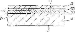
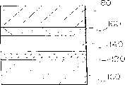
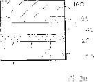
[1]如图1所示,在基板1的一个面上(分离层形成面11)上形成分离层(光吸收层)2。基板1是在从基板1一侧照射照射光7时具有能透过该照射光7的透光性的基板,这一点是较为理想的。此时,照射光7的透射率是10%以上是较为理想的,是50%以上更为理想。如果该透射率过低,则照射光7的衰减(loss)变大,由于剥离分离层而需要大的光量。[1] As shown in FIG. 1 , a separation layer (light absorbing layer) 2 is formed on one surface (separation layer formation surface 11 ) of a
此外,用可靠性高的材料构成基板1是较为理想的,特别是用耐热性优良的材料构成是较为理想的。其原因是因为:例如在形成下述的被转移层4及中间层3时,有时因其种类或形成方法之故工艺温度变高(例如350~1000℃左右),但即使在该情况下,如果基板1在耐热性方面优良,则在向基板1上的被转移层4等的形成时,该温度条件等的成膜条件的设定的范围变宽。In addition, it is preferable to form the
因而,在将被转移层4的形成时的最高温度设为Tmax时,用变形点为Tmax以上的材料构成基板1是较为理想的。具体地说,基板1的构成材料的变形点在350℃以上是较为理想的,在500℃以上更为理想。作为这样的材料,例如可举出石英玻璃、钠玻璃、康宁(corning)7059、日本电气玻璃0A-2等耐热性玻璃。Therefore, when the maximum temperature at the time of forming the transferred layer 4 is Tmax, it is preferable to form the
再有,如果降低下述的分离层2、中间层3和被转移层4的形成时的工艺温度,则对于基板1也可使用熔点低的廉价的玻璃材料及合成树脂。Furthermore, if the process temperature for forming the
此外,基板1的厚度虽不特别限定,但一般厚度为约0.1~5.0mm是较为理想的,厚度为约0.5~1.5mm更为理想。如果基板1的厚度过薄,则导致强度的降低,如果过厚,则在基板1的透射率低的情况下,容易产生照射光7的衰减。再有,在基板1的照射光7的透射率高的情况下,基板1的厚度也可超过上述上限值。In addition, although the thickness of the
再有,基板1的分离层形成部分的厚度是均匀的,以便能使照射光7均匀地照射,这一点是较为理想的。此外,基板1的分离层形成面11及照射光入射面12不限于如图示那样是平面,也可以是曲面。在本发明中,不用刻蚀等除去基板1,而是剥离存在于基板1和被转移层4之间的分离层2来使基板1脱离,故操作是容易的,同时,例如使用比较厚的基板等,关于基板1的选择的范围也变宽。In addition, it is desirable that the thickness of the part where the separation layer is formed on the
其次,说明分离层2。分离层2具有吸收后面叙述的照射光7,在该层内和/或界面处2a或2b产生剥离(以下称为「层内剥离」、「界面剥离」)的性质,较为理想的是,利用照射光7的照射,通过构成分离层2的物质的原子间或分子间的结合力消失或减少,实际上是产生剥离等,来达到层内剥离和/或界面处剥离。再者,也有利用照射光7的照射,从分离层2放出气体,从而显现出分离效果的情况。即,存在下述情况:在分离层2中含有的成分变成气体而放出的情况和分离层2吸收光在一瞬间变成气体,该蒸汽被放出,从而有助于分离的情况。Next, the
作为这样的分离层2的组成,可举出例如以下的①~⑥。Examples of the composition of such a
①非晶硅(a-Si):① Amorphous silicon (a-Si):
在该非晶硅中可含有H(氢)。此时,H的含有量在约2at%以上是较为理想的,在约2~20at%更为理想。因此,如果含有规定量的H,则利用照射光7的照射,将氢放出,在分离层2内发生内压,该内压成为剥离上下的薄膜的力。可通过适当地设定成膜条件、例如CVD中的气体组成、气体压力、气体气氛、气体流量、温度、基板温度、输入功率等的条件,来调整非晶硅中的H的含有量。H (hydrogen) may be contained in this amorphous silicon. In this case, the H content is preferably about 2 at % or more, more preferably about 2 to 20 at %. Therefore, if a predetermined amount of H is contained, hydrogen is released by the irradiation of the
②氧化硅或硅酸盐、氧化钛或钛酸盐、氧化锆或锆酸盐、氧化镧或镧酸盐等的各种氧化物陶瓷、电介质(强电介质)或半导体:② Various oxide ceramics, dielectrics (ferroelectrics) or semiconductors such as silicon oxide or silicate, titanium oxide or titanate, zirconia or zirconate, lanthanum oxide or lanthanate:
作为上述的氧化硅,可举出SiO、SiO2、Si3O2,作为硅酸盐,可举出例如K2SiO3、Li2SiO3、CaSiO3、ZrSiO4、Na2SiO3。作为上述的氧化钛,可举出TiO、Ti2O3、TiO2,作为钛酸盐,可举出例如BaTiO4、BaTiO3、Ba2Ti9O20、BaTi5O11、CaTiO3、SrTiO3、PbTiO3、MgTiO3、ZrTiO2、SnTiO4、Al2TiO5、FeTiO3。作为上述的氧化锆,可举出ZrO2,作为锆酸盐,例如可举出BaZrO3、ZrSiO4、PbZrO3、MgZrO3、K2ZrO3。Examples of silicon oxide include SiO, SiO2 , and Si3 O2 , and examples of silicate include K2 SiO3 , Li2 SiO3 , CaSiO3 , ZrSiO4 , and Na2 SiO3 . Examples of the aforementioned titanium oxide include TiO, Ti2 O3 , and TiO2 , and examples of titanates include BaTiO4 , BaTiO3 , Ba2 Ti9 O20 , BaTi5 O11 , CaTiO3 , and SrTiO.3. PbTiO3 , MgTiO3 , ZrTiO2 , SnTiO4 , Al2 TiO5 , FeTiO3 . Examples of the above-mentioned zirconia include ZrO2 , and examples of zirconates include BaZrO3 , ZrSiO4 , PbZrO3 , MgZrO3 , and K2 ZrO3 .
③PZT、PLZT、PLLZT、PBZT等的陶瓷或电介质(强电介质):③PZT, PLZT, PLLZT, PBZT and other ceramics or dielectrics (ferroelectric):
④氮化硅、氮化铝、氮化钛等的氮化物陶瓷:④ Nitride ceramics of silicon nitride, aluminum nitride, titanium nitride, etc.:
⑤有机高分子材料:⑤Organic polymer materials:
作为有机高分子材料,是具有-CH2-、-CO-(酮)、-CONH-(胺)、-NH-(亚氨)、-COO-(酯)、-N=N-(偶氮)、-CH=N-(异氰)等的结合(利用照射光7的照射切断这些结合)的材料,特别是如果是具有多个这些结合的材料,则什么样的材料都可以。此外,有机高分子材料可以是在其构成式中具有芳香烃(1或2个以上的苯环或其缩合环)的材料。作为这样的有机高分子材料的具体例,可举出聚乙烯、聚丙烯那样的聚烯烃、聚酰亚胺、聚酰胺、聚酯、聚甲基丙烯酸甲酯(PMMA)、聚苯撑硫(PPS)、聚醚砜(PES)、环氧树脂等。As an organic polymer material, there are -CH2 -, -CO-(ketone), -CONH-(amine), -NH-(imino), -COO-(ester), -N=N-(azo ), -CH=N-(isocyan), etc. (these bonds are cut by the irradiation of the irradiation light 7), especially if it is a material having a plurality of these bonds, any material may be used. In addition, the organic polymer material may be a material having an aromatic hydrocarbon (one or more benzene rings or condensed rings thereof) in its constitutional formula. Specific examples of such organic polymer materials include polyolefins such as polyethylene and polypropylene, polyimides, polyamides, polyesters, polymethyl methacrylate (PMMA), polyphenylene sulfide ( PPS), polyethersulfone (PES), epoxy resin, etc.
⑥金属:⑥Metal:
作为金属,例如可举出Al、Li、Ti、Mn、In、Sn、Y、La、Ce、Nd、Pr、Gd、Sm或包含这些金属中的至少一种的合金。Examples of metals include Al, Li, Ti, Mn, In, Sn, Y, La, Ce, Nd, Pr, Gd, Sm, or alloys containing at least one of these metals.
其次,分离层2的厚度根据剥离目的及分离层2的组成、层构成、形成方法等的诸条件的不同而不同,但通常约1nm~20微米是较为理想的,约10nm~2微米则更为理想,约40nm~1微米则还要理想。如果分离层2的厚度过小,则有时成膜的均匀性受到损害,在剥离中产生不平整,此外,如果膜厚过厚,则为了确保分离层2的良好的剥离性,必须增大照射光7的功率(光量),同时在之后的除去分离层2时,其操作很费时。再有,分离层2的膜厚最好尽可能均匀。Next, the thickness of the
分离层2的形成方法不作特别限定,可根据膜组成及膜厚等诸条件进行适当的选择。例如,可举出CVD(包含MOCVD、低压CVD、ECR-CVD)、蒸镀、分子束蒸镀(MB)、溅射、离子镀、PVD等各种气相成膜法、电镀、浸镀(dipping)、无电解镀等的各种镀法,Langmuir-Blodgett(LB)法、旋转涂敷、喷镀涂敷(spray coat)、滚动涂敷(rollcoat)等的涂敷法、各种印刷法、转移法、喷墨法、喷粉法等,也可将这些方法中的2种以上的方法组合起来形成。在例如分离层2的组成是非晶硅(a-Si)的情况下,利用CVD、特别是低压CVD及等离子CVD来成膜是较为理想的。此外,在用溶胶-凝胶法产生的陶瓷构成分离层2的情况下或在用有机高分子材料构成分离层2的情况下,利用涂敷法、特别是旋转涂敷法来成膜是较为理想的。此外,也可用2个工序以上的工序(例如,层的形成工序和热处理工序)来进行分离层2的形成。The method for forming the
[2]如图2所示,在分离层2上形成中间层(基底层)3。[2] As shown in FIG. 2 , an intermediate layer (base layer) 3 is formed on the
该中间层3以各种形成目的来形成,例如可举出发挥作为在制造时或使用时以物理或化学的方式保护下述被转移层4的保护层、绝缘层、导电层、照射光7的遮光层、阻止向被转移层4的或来自被转移层4的成分的迁移(migration)的阻档层、反射层的功能中的至少一种的目的。The
作为该中间层3的组成,可根据其形成目的适当地设定,例如,在非晶硅的分离层2和薄膜晶体管的被转移层4之间形成的中间层的情况下,可举出SiO2等氧化硅,在分离层2和PZT的被转移层4之间形成的中间层3的情况下,例如可举出Pt、Au、W、Ta、Mo、Al、Cr、Ti或以这些金属为主的合金那样的金属。这样的中间层3的厚度根据其形成目的及能发挥的功能的程度适当地决定,但通常约10nm~5微米是较为理想的,约40nm~1微米则更为理想。此外,关于中间层3的形成方法,也可举出与在上述分离层2中举出的形成方法相同的方法。此外,也可用2个工序以上的工序来进行中间层3的形成。The composition of the
再有,也可用2层以上的相同或不同的组成的层来形成这样的中间层3。此外,在本发明中,也可不形成中间层3,直接在分离层2上形成被转移层4。In addition, such an
[3]如图3所示,在中间层3上形成被转移层(被剥离物)4。被转移层4是转移到下面叙述的转移体6上的层,可用与上述分离层2中举出的形成方法相同的方法来形成。[3] As shown in FIG. 3 , a transferred layer (to-be-striped object) 4 is formed on the
被转移层4的形成目的、种类、形态、结构、组成、物理或化学特性等不作特别限定,但考虑转移的目的及有用性,是薄膜、特别是功能性薄膜及薄膜器件是较为理想的。作为功能性薄膜或薄膜器件,例如可举出:薄膜晶体管、薄膜二极管、其他的薄膜器件、电极(例:ITO、台面膜那样的透明电极)、太阳电池及图象传感器等中使用的光电转换元件、开关元件、存储器、压电元件等的致动器(actuator)、微镜(micro mirror)(压电薄膜陶瓷)、磁记录媒体、磁光记录媒体、光记录媒体等的记录媒体、磁记录薄膜头、线圈、电感器、薄膜高透磁材料和将其组合起来的微磁器件、滤光器、反射膜、分色镜、偏光元件等光学薄膜、半导体薄膜、超导薄膜(例:YBCO薄膜)、磁性薄膜、金属多层薄膜、金属陶瓷多层薄膜、金属半导体多层薄膜、陶瓷半导体多层薄膜、有机薄膜与其他物质的多层薄膜等。在其中,特别是应用于薄膜器件、微磁器件、微三维结构物的构成、致动器(actuator)、微镜(micro mirror)等的有用性很高、是较为理想的。The formation purpose, type, shape, structure, composition, physical or chemical properties of the transferred layer 4 are not particularly limited, but considering the purpose and usefulness of the transfer, thin films, especially functional thin films and thin film devices are ideal. Examples of functional thin films or thin film devices include thin film transistors, thin film diodes, other thin film devices, electrodes (for example: transparent electrodes such as ITO and mesa films), solar cells, and photoelectric conversion devices used in image sensors. Elements, switching elements, memories, actuators such as piezoelectric elements, micro mirrors (piezoelectric thin film ceramics), magnetic recording media, magneto-optical recording media, optical recording media and other recording media, magnetic Recording film heads, coils, inductors, thin film high magnetic permeability materials and micromagnetic devices combined with them, optical filters, reflective films, dichroic mirrors, polarizing elements and other optical films, semiconductor films, superconducting films (for example: YBCO film), magnetic film, metal multilayer film, cermet multilayer film, metal semiconductor multilayer film, ceramic semiconductor multilayer film, organic film and multilayer film of other substances, etc. Among them, application to thin film devices, micromagnetic devices, formation of micro three-dimensional structures, actuators, micro mirrors, etc. is highly useful and ideal.
这样的功能性薄膜或薄膜器件,由于与其形成方法的关系,通常经过较高的工艺温度来形成。因而,在这种情况下,如上所述,作为基板1,必须是能耐该工艺温度的可靠性高的基板。Such a functional thin film or thin film device is usually formed at a relatively high process temperature due to its formation method. Therefore, in this case, as described above, the
再有,被转移层4可以是单层,也可以是多层的层叠体。再者,如上述的薄膜晶体管等那样,可以是进行了规定的图形刻蚀的被转移层。被转移层4的形成(层叠)、图形刻蚀,利用与其对应的方法来进行。这样的被转移层4通常经过多个工序而形成。In addition, the transferred layer 4 may be a single layer or a laminated body of multiple layers. Furthermore, like the above-mentioned thin film transistor, etc., it may be a transfer target layer etched with a predetermined pattern. Formation (stacking) and pattern etching of the transferred layer 4 are carried out by corresponding methods. Such transferred layer 4 is usually formed through a plurality of steps.
关于薄膜晶体管的被转移层4的形成,例如可按照特公平2-50630号公报、文献:H.Ohshima et al:International Symposium Digest ofTechnical Papers SID 1983“用多晶硅TFTs寻址的黑白和彩色LC视频显示器”中所述的方法来进行。Regarding the formation of the transferred layer 4 of the thin film transistor, for example, according to the Japanese Patent Publication No. 2-50630, document: H.Ohshima et al: International Symposium Digest of Technical Papers SID 1983 "Black and white and color LC video display with polysilicon TFTs addressing " by the method described in.
此外,被转移层4的厚度不作特别限定,可根据其形成目的、功能、组成、特性等诸条件适当地设定。在被转移层4是薄膜晶体管的情况下,其合计厚度约为0.5~200微米是较为理想的,约为0.5~10微米则更为理想。此外,在其他的薄膜的情况下,优选的合计厚度的范围可更宽,例如可定为50nm~1000微米。In addition, the thickness of the transferred layer 4 is not particularly limited, and can be appropriately set according to various conditions such as its formation purpose, function, composition, and characteristics. When the transferred layer 4 is a thin film transistor, its total thickness is preferably about 0.5 to 200 microns, and more preferably about 0.5 to 10 microns. In addition, in the case of other thin films, the range of preferable total thickness can be wider, for example, it can set it as 50 nm - 1000 micrometers.
再有,被转移层4不限定于上述的那样的薄膜,例如也可以是涂敷膜及薄片那样的厚膜,再者,例如也可以是粉体那样的不构成膜(层)的被转移物或被剥离物。Furthermore, the to-be-transferred layer 4 is not limited to the above-mentioned thin film, for example, it may also be a thick film such as a coating film or a sheet, and, for example, it may also be a to-be-transferred layer that does not constitute a film (layer) such as a powder. objects or objects to be stripped.
[4]如图4所示,在被转移层(被剥离物)4上形成粘接层5,通过该粘接层5粘接(接合)转移体6。作为构成粘接层5的粘接剂的优选例,可举出反应硬化型粘接剂、热硬化型粘接剂、紫外线硬化型粘接剂等的光硬化型粘接剂、厌气硬化型粘接剂等各种硬化型粘接剂。作为粘接剂的组成,例如可以是环氧系列、丙烯酸系列、硅酮系列等的任一种。这样的粘接层5的形成,例如可用涂敷法来进行。[4] As shown in FIG. 4 , an
在使用上述硬化型粘接剂的情况下,例如在被转移层4上涂敷硬化型粘接剂,在其上接合了下述的转移体6之后,利用与硬化型粘接剂的特性对应的硬化方法使上述硬化型粘接剂硬化,将被转移层4与转移体6粘接、固定起来。在使用光硬化型粘接剂的情况下,最好在未硬化的粘接层5上配置了透光性的转移体6之后,从转移体6上照射硬化用的光,使粘接剂硬化。此外,如果基板1具有透光性,则最好从基板1和转移体6的两侧照射硬化用的光,使粘接剂硬化,使硬化变得可靠。In the case of using the above-mentioned hardening adhesive, for example, the hardening adhesive is applied to the transferred layer 4, and after the
再有,与图示不同,也可在转移体6一侧形成粘接层5,在其上粘接被转移层4。此外,也可在被转移层4与粘接层5之间设置上述那样的中间层。此外,例如在转移体6本身具有粘接功能的情况下,也可省略粘接层5的形成。In addition, unlike the illustration, the
作为转移体6,不作特别限定,可举出基板(板材)、特别是透明基板。再有,这样的基板可以是平板,也可以是弯曲板。此外,转移体6与上述基板1相比,可以说耐热性、耐腐蚀性等的特性较差的基板。其原因是因为,由于在本发明中在基板1一侧形成被转移层4,其后将该被转移层4转移到转移体6上,故对转移体6要求的特性,特别是耐热性,与被转移层4形成时的温度条件等无关。It does not specifically limit as the
因而,在将被转移层4的形成时的最高温度设为Tmax时,可用玻璃转变点(Tg)或软化点为Tmax以下的材料作为转移体6的构成材料。例如,可用玻璃转变点(Tg)或软化点为800℃以下材料构成转移体6是较为理想的,500℃以下更为理想,300℃以下还要理想。Therefore, when the highest temperature at the time of forming the transferred layer 4 is Tmax, a material having a glass transition point (Tg) or a softening point equal to or lower than Tmax can be used as a constituent material of the
此外,作为转移体6的机械特性,具有某种程度的刚性(强度)是较为理想的,但也可以具有可挠性、弹性。作为这样的转移体6的构成材料,可举出各种合成树脂及各种玻璃材料,特别是各种合成树脂或普通的(低熔点的)廉价的玻璃材料是较为理想的。In addition, as the mechanical characteristics of the
作为合成树脂,可以是热可塑性树脂、热硬化性树脂的任一种。例如可举出:聚乙烯、聚丙烯、乙烯-丙烯共聚体、乙烯-乙酸乙烯共聚体(EVA)等的聚烯烃、环状聚烯烃、变性聚烯烃、聚氯乙烯、聚氯乙二烯、聚苯乙烯、聚酰胺、聚酰亚胺、聚酰胺亚胺、聚碳酸酯、聚-(4-甲基戊烯-1)、离聚物、丙烯酸系列树脂、聚甲基丙烯酸甲酯(PMMA)、丙烯腈-丁二烯-苯乙烯共聚体(ABS树脂)、丙烯腈-苯乙烯共聚体(AS树脂)、丁二烯-苯乙烯共聚体、聚甲醛、聚乙烯醇(PVA)、乙烯-乙烯醇共聚体(EVOH)、聚乙烯对苯二甲酸盐(PET)、聚丁烯对苯二甲酸盐(PBT)、多环己烷对苯二甲酸盐(PCT)等的聚酯、聚醚、聚醚酮(PEK)、聚醚乙醚酮(PEEK)、聚醚亚胺、聚醛(POM)、聚苯撑氧、变性聚苯撑氧、聚砜、聚苯撑硫(PPS)、聚醚砜(PES)、多芳基化合物、芳香族聚酯(液晶聚合物)、聚四氟乙烯、聚偏氟乙烯、其他的氟系列树脂、苯乙烯系列、聚烯烃系列、聚氯乙烯系列、聚氨酯系列、聚酯系列、聚酰胺系列、聚丁二烯系列、反聚异戊二烯系列、氟橡胶系列、氯化聚乙烯系列等的各种热可塑性弹性体、环氧树脂、酚树脂、脲树脂、蜜胺树脂、不饱和聚酯、硅酮树脂、聚氨基甲酸酯等,或以这些为主的共聚体、混合体、聚合物混合体等,可以将这些物质中的1种或2种以上组合起来(例如作为2层以上的层叠体)使用。The synthetic resin may be either a thermoplastic resin or a thermosetting resin. Examples include polyolefins such as polyethylene, polypropylene, ethylene-propylene copolymers, and ethylene-vinyl acetate copolymers (EVA), cyclic polyolefins, denatured polyolefins, polyvinyl chloride, polyvinyl chloride, Polystyrene, polyamide, polyimide, polyamide imide, polycarbonate, poly-(4-methylpentene-1), ionomer, acrylic series resin, polymethyl methacrylate (PMMA ), acrylonitrile-butadiene-styrene copolymer (ABS resin), acrylonitrile-styrene copolymer (AS resin), butadiene-styrene copolymer, polyoxymethylene, polyvinyl alcohol (PVA), ethylene -Polymers such as vinyl alcohol copolymer (EVOH), polyethylene terephthalate (PET), polybutylene terephthalate (PBT), polycyclohexane terephthalate (PCT), etc. Ester, polyether, polyether ketone (PEK), polyether ether ketone (PEEK), polyetherimide, polyaldehyde (POM), polyphenylene oxide, denatured polyphenylene oxide, polysulfone, polyphenylene sulfide ( PPS), polyethersulfone (PES), polyarylate, aromatic polyester (liquid crystal polymer), polytetrafluoroethylene, polyvinylidene fluoride, other fluorine series resins, styrene series, polyolefin series, poly Various thermoplastic elastomers and epoxy resins such as vinyl chloride series, polyurethane series, polyester series, polyamide series, polybutadiene series, reverse polyisoprene series, fluororubber series, chlorinated polyethylene series, etc. , phenol resin, urea resin, melamine resin, unsaturated polyester, silicone resin, polyurethane, etc., or copolymers, mixtures, polymer mixtures, etc. based on these substances, which can be used One or more of them are used in combination (for example, as a laminate of two or more layers).
作为玻璃材料,例如可举出硅酸盐玻璃(石英玻璃)、含碱的硅酸盐玻璃、碱石灰玻璃、钾石灰玻璃、铅(含碱的)玻璃、钡玻璃、硼硅酸玻璃等。其中,除了硅酸盐玻璃以外的玻璃与硅酸盐玻璃相比,熔点低、此外,成形加工也比较容易,而且廉价,故是较为理想的。Examples of glass materials include silicate glass (quartz glass), alkali-containing silicate glass, soda lime glass, potassium lime glass, lead (alkali-containing) glass, barium glass, borosilicate glass, and the like. Among them, glasses other than silicate glass are preferable because they have a lower melting point than silicate glass, and are relatively easy to form and process, and are also inexpensive.
在使用由合成树脂构成的转移体6的情况下,能获得下述的各种优点:可一体地成形大型的转移体6,同时即使具有弯曲面或凹凸等的复杂形状也可容易地制造,此外,材料成本、制造成本也是廉价的。因而,能容易地制造大型而且廉价的装置(例如,液晶显示器)。In the case of using the
再有,转移体6可以是例如液晶单元那样的构成本身独立的器件的单元,也可以是例如彩色滤光器、电极层、电介质层、绝缘层、半导体元件那样的构成器件的一部分的单元。再者,转移体6可以是金属、陶瓷、石材、木材、纸等物质,也可以是构成某种物品的任意的面上(钟表的面上、空调器的表面上、印刷基板上等)、或是壁、柱、梁、天花板、窗玻璃等的结构物的表面上。Furthermore, the
[5]如图5所示,从基板1的背面一侧使照射光7(照射光入射面12一侧)照射。在该照射光7透过了基板1之后,从界面2a一侧照射到分离层2上。由此,如图6或7所示,由于在分离层2中产生层内剥离和/或界面处剥离,结合力减少或消失,故如果使基板1与转移体6脱离,则被转移层4从基板1脱离,转移到转移体6上。[5] As shown in FIG. 5 , the irradiation light 7 (the irradiation
再有,图6示出在分离层2中产生层内剥离的情况,图7示出在分离层2中产生界面2a处的界面剥离的情况。假定产生分离层2中的层内剥离和/或界面处剥离的原理是由于在分离层2的构成材料中产生剥离,或分离层2内含有的气体的放出、再有是由于刚照射后产生的熔融、蒸发等的相变化。6 shows the case where intralayer delamination occurs in the
这里,所谓剥离(ablation),指的是以光化学或热的方式激励吸收了照射光的固体材料(分离层2的构成材料),切断其表面及内部的原子或分子的结合而使其放出,主要作为产生分离层2的构成材料的全部或一部分熔融、蒸发(气化)等相变化的现象而显现出来。此外,也有由于上述相变化而变成微小的发泡状态,结合力降低的情况。分离层2产生层内剥离,或是产生界面剥离,或是产生这两种剥离,这一点是由分离层2的组成、及其他各种主要原因来决定,作为其主要原因之一,可举出照射光7的种类、波长、强度、到达深度等的条件。Here, the so-called "ablation" refers to photochemically or thermally exciting the solid material (the constituent material of the separation layer 2) that absorbs the irradiated light, cutting off the bonding of atoms or molecules on the surface and inside thereof, and releasing them. It appears mainly as a phenomenon in which all or a part of the constituent materials of the
作为照射光7,只要是在分离层2内引起层内剥离和/或界面处剥离的光,则可以是任一种光,例如,可举出:X线、紫外线、可视光、红外线(热线)、激光、毫米波、微波、电子线、放射线(α线、β线、γ线)等,但尤其是从容易产生分离层2的剥离(ablation)方面考虑,激光是较为理想的。As the
作为发生该激光的激光装置,可举出各种气体激光、固体激光(半导体激光)等,但可优选使用受激准分子激光、Nd-YAG激光、Ar激光、CO2激光、CO激光、He-Ne激光等,尤其是受激准分子激光特别理想。由于受激准分子激光在短波长波段输出高的能量,故可在极短时间内在分离层2中产生剥离,于是可剥离分离层2而在相邻的或附近的中间层3、被转移层4、基板1等中几乎不使温度上升,即不产生性能变坏、损伤。Examples of laser devices that generate this laser light include various gas lasers, solid-state lasers (semiconductor lasers), etc., but excimer lasers, Nd-YAG lasers, Ar lasers,CO2 lasers, CO lasers, He -Ne laser etc., especially an excimer laser is particularly preferable. Since the excimer laser outputs high energy in the short wavelength band, peeling can occur in the
此外,在分离层2中产生剥离时的照射光中存在波长依存性的情况下,所照射的激光的波长是约100~350nm是较为理想的。In addition, when there is wavelength dependence in the irradiation light when peeling occurs in the
此外,在分离层2中例如引起气体放出、气化、升华等的相变化而提供分离特性的情况下,所照射的激光的波长是约350~1200nm是较为理想的。In addition, in the case of providing separation characteristics by causing phase changes such as gas evolution, vaporization, and sublimation in the
此外,所照射的激光的能量密度,特别是受激准分子激光的情况下的能量密度定为约10~5000mJ/cm2是较为理想的,定为约100~1000mJ/cm2则更为理想。此外,照射时间定为约1~1000nsec是较为理想的,定为约10~100nsec则更为理想。如果能量密度低或照射时间短,则不能产生充分的剥离,此外,如果能量密度高或照射时间长,则有时由于透过分离层2及中间层3的照射光而对被转移层4产生不良影响。In addition, the energy density of the laser light to be irradiated, especially in the case of an excimer laser, is preferably about 10 to 5000 mJ/cm2 , more preferably about 100 to 1000 mJ/cm2 . In addition, the irradiation time is preferably about 1 to 1000 nsec, more preferably about 10 to 100 nsec. If the energy density is low or the irradiation time is short, sufficient peeling cannot occur. In addition, if the energy density is high or the irradiation time is long, the transfer layer 4 may be damaged due to the irradiation light passing through the
以这样的激光为代表的照射光7以其强度成为均匀的这种方式进行照射是较为理想的。照射光7的照射方向不限于相对于分离层2为垂直的方向,也可以是相对于分离层2为倾斜了规定角度的方向。It is desirable to irradiate the
此外,在分离层2的面积比照射光的1次的照射面积大的情况下,也可相对于分离层2的全部区域分成多次来使照射光照射。此外,也可对同一部位照射2次以上。此外,也可对同一区域或不同区域照射不同种类、不同波长(波长波段)的照射光(激光)2次以上。In addition, when the area of the
[6]如图8所示,例如利用清洗、刻蚀、灰化(ashing)、研磨等方法或将这些方法组合起来的方法来除去附着于中间层3上的分离层2。在图6中示出的那种分离层2的层内剥离的情况下,也以同样的方式除去附着于基板1上的分离层2。[6] As shown in FIG. 8 , the
再有,在基板1用石英玻璃那样的高价材料、稀有材料构成的情况下,最好将基板1再次利用(recycle)。换言之,对于打算再次利用的基板1,可应用本发明,有用性很高。Furthermore, when the
经过以上那样的各工序,就完成了被转移层4的向转移体6的转移。其后,也可进行与被转移层4相邻的中间层3的除去及其他的任意的层的形成等。Through the above steps, the transfer of the transferred layer 4 to the
在本发明中,由于不是直接剥离被剥离物、即被转移层4本身,而是在接合到被转移层4的分离层2中进行剥离,故不管被剥离物(被转移层4)的特性、条件等如何,能容易、可靠而且均匀地剥离(转移),可维持被转移层4的高的可靠性,而没有伴随剥离操作的对于被剥离物(被转移层4)的损伤。In the present invention, since the object to be peeled, i.e., the transferred layer 4 itself, is not directly peeled off, but is peeled in the
此外,在图示的实施例中,关于被转移层4的向转移体6的转移方法进行了说明,但本发明的转移方法也可不进行这样的转移。在这种情况下,可作成被剥离物来代替上述的被转移层4。该被剥离物可以是层状的物质、不构成层的物质的任一种。In addition, in the illustrated embodiment, the transfer method of the transfer target layer 4 to the
此外,被剥离物的剥离目的,例如可以是上述那样的薄膜(特别是功能性薄膜)的不需要的部分的除去(修整trimming)、尘埃、氧化物、重金属、碳、其他杂质等的附着物的除去、利用了该除去的基板等的再循环(recycle)等的任一种。In addition, the purpose of peeling the object to be peeled may be, for example, the removal of unnecessary parts of the above-mentioned thin film (especially a functional thin film) (trimming), attachment of dust, oxides, heavy metals, carbon, other impurities, etc. Any of the removal of the substrate and the recycling of the substrate or the like using the removal.
此外,转移体6不限于上述的材料,例如也可用各种金属材料、陶瓷、碳、纸材料、橡胶等与基板1性质完全不同的材料(不管是否有透光性)来构成。特别是在转移体6是不能直接形成被转移层4,或不适合于形成被转移层4的材料的情况下,应用本发明的价值很高。In addition, the
此外,在图示的实施例中,使照射光7从基板1一侧照射,但例如在除去附着物(被剥离物)的情况下,及在被转移层4不因照射光7的照射而受到不良影响的情况下,照射光7的照射方向不限于上述方向,也可使照射光从与基板1相反的一侧照射。In addition, in the illustrated embodiment, the
以上,关于图示的实施例说明了本发明的剥离方法,但本发明不限定于此。As mentioned above, although the peeling method of this invention was demonstrated about the Example shown in figure, this invention is not limited to this.
例如,也可以是相对于分离层2的面方向局部地、即,使照射光以规定的图形来照射,以上述图形来剥离或转移被转移层4那样的构成(第1方法)。在这种情况下,在上述[5]的工序中,相对于基板1的照射光入射面12,进行对应于上述图形的掩模操作(masking)使照射光7照射,或是利用精密地控制照射光7的照射位置等方法来进行。For example, a configuration may be adopted in which the transferred layer 4 is peeled or transferred in the above-mentioned pattern by irradiating irradiation light locally in a predetermined pattern with respect to the plane direction of the separation layer 2 (first method). In this case, in the above-mentioned step [5], masking operation (masking) corresponding to the above-mentioned pattern is performed on the irradiation
此外,也能够不是在基板1的分离层形成面11的整个面上形成分离层2,而是以规定的图形来形成分离层2(第2方法)。此时,可利用掩模操作等将分离层2形成为预先规定的图形,或可在分离层形成面11的整个面上形成分离层2后,利用刻蚀等进行图形刻蚀或修整的方法。In addition, instead of forming the
按照以上那样的第1方法和第2方法,与该图形刻蚀或修整一起进行被转移层4的转移。Transfer of the transferred layer 4 is carried out together with the pattern etching or trimming according to the above-mentioned first method and second method.
此外,也可利用与上述方法相同的方法重复进行2次以上的转移。此时,如果转移次数是偶数次,则也可使在最后的转移体上形成的被转移层的表面·背面的位置关系与最初在基板1上形成了被转移层的状态相同。In addition, the transfer may be repeated two or more times by the same method as the above-mentioned method. At this time, if the number of transfers is an even number, the positional relationship between the front and rear surfaces of the transferred layer formed on the final transfer body may be the same as the state in which the transferred layer was first formed on the
此外,也可将大型的透明基板(例如,有效区域为900mm×1600mm)作为转移体6,较为理想的是,将在小型的基板1(例如,有效区域为45mm×40mm)上形成了的小单位的被转移层4(薄膜晶体管)顺序地多次(例如,约800次)转移到邻接的位置上,在大型透明基板的整个有效区域上形成被转移层4,最终制造与上述大型透明基板尺寸相同的液晶显示器。In addition, a large transparent substrate (for example, an effective area of 900mm×1600mm) can also be used as the
其次,说明第1实施形态中的具体的实施例。Next, specific examples in the first embodiment will be described.
(实施例1)(Example 1)
准备纵50mm×横50mm×厚度1.1mm的石英基板(软化点:1630℃,变形点:1070℃,受激准分子激光的透射率:大致100%),在该石英基板的一个面上,利用低压CVD法(Si2H6气体,425℃)形成非晶硅(a-Si)膜作为分离层(激光吸收层)。分离层的膜厚是100nm。A quartz substrate (softening point: 1630° C., deformation point: 1070° C., excimer laser transmittance: approximately 100%) of 50 mm in length × 50 mm in width × 1.1 mm in thickness was prepared, and on one surface of the quartz substrate, the A low-pressure CVD method (Si2 H6 gas, 425° C.) forms an amorphous silicon (a-Si) film as a separation layer (laser absorption layer). The film thickness of the separation layer was 100 nm.
其次,在分离层上利用ECR-CVD法(SiH4+O2气体,100℃)形成SiO2膜作为中间层。中间层的膜厚是200nm。Next, a SiO2 film was formed as an intermediate layer on the separation layer by ECR-CVD (SiH4 +O2 gas, 100° C.). The film thickness of the intermediate layer was 200 nm.
其次,在中间层上利用CVD法(Si2H6气体)形成膜厚为50nm的多晶硅膜作为被转移层。其后,对该多晶硅膜进行规定的图形刻蚀,形成成为薄膜晶体管的源·漏·沟道的区域。其后,用1000℃以上的高温对多晶硅膜的表面进行热氧化形成了栅绝缘膜SiO2后,在栅绝缘膜上形成栅电极(在多晶硅上层叠形成了Mo等高熔点的金属的结构),通过以栅电极为掩模进行离子注入,以自对准的方式形成源·漏区,从而形成薄膜晶体管。Next, a polysilicon film with a film thickness of 50 nm was formed on the intermediate layer by CVD (Si2 H6 gas) as a transferred layer. Thereafter, a predetermined pattern is etched on the polysilicon film to form regions to be source, drain, and channel of the thin film transistor. Thereafter, the surface of the polysilicon film is thermally oxidized at a high temperature of 1000°C or higher to form a gate insulating filmSiO2 , and then a gate electrode is formed on the gate insulating film (a structure in which a high-melting-point metal such as Mo is stacked on polysilicon) , by performing ion implantation using the gate electrode as a mask to form source and drain regions in a self-aligned manner, thereby forming a thin film transistor.
再有,不是使用上述那样的高温工艺,而是使用低温工艺也可形成同样的特性的薄膜晶体管。例如,在分离层上,在作为中间层的SiO2膜上利用低压CVD法(Si2H6气体,425℃)形成50nm的非晶硅膜作为被转移层,对该非晶硅膜照射激光(波长308nm),使其结晶化,成为多晶硅膜。其后,对于该多晶硅膜进行规定的图形刻蚀,形成成为薄膜晶体管的源·漏·沟道的区域。其后,利用低压CVD法在多晶硅膜上淀积了栅绝缘膜SiO2后,在栅绝缘膜上形成栅电极(在多晶硅上层叠形成了Mo等高熔点的金属的结构),通过以栅电极为掩模进行离子注入,以自对准(self align)的方式形成源·漏区,从而形成薄膜晶体管。In addition, a thin film transistor having the same characteristics can be formed by using a low-temperature process instead of the above-mentioned high-temperature process. For example, on the separation layer, a 50 nm amorphous silicon film is formed as a transferred layer by low-pressure CVD (Si2 H6 gas, 425° C.) on a SiO2 film as an intermediate layer, and the amorphous silicon film is irradiated with laser light. (wavelength 308nm), make it crystallized, and become a polysilicon film. Thereafter, predetermined pattern etching is performed on the polysilicon film to form regions to be source, drain, and channel of the thin film transistor. After that, a gate insulating filmSiO2 was deposited on the polysilicon film by low-pressure CVD, and a gate electrode (a structure in which a high-melting-point metal such as Mo was stacked on polysilicon) was formed on the gate insulating film. Ion implantation is performed for the mask to form source and drain regions in a self-aligned manner, thereby forming a thin film transistor.
其后,根据需要,形成与源·漏区连接的电极和布线、与栅电极连接的布线。在这些电极及布线中使用Al,但不限定于此。此外,在担心因后工序的激光照射而产生Al的熔融的情况下,也可使用比Al的熔点高的金属(因后工序的激光照射不熔融的金属)。Thereafter, electrodes and wirings connected to the source/drain regions, and wirings connected to the gate electrodes are formed as necessary. Although Al is used for these electrodes and wirings, it is not limited thereto. In addition, when there is concern about melting of Al by laser irradiation in a post-process, a metal having a higher melting point than Al (a metal that does not melt by laser irradiation in a post-process) may be used.
其次,在上述薄膜晶体管上涂敷紫外线硬化型粘接剂(膜厚:100微米),再者在该涂膜上接合了作为转移体的纵200mm×横300mm×厚度1.1mm的大型的透明玻璃基板(钠玻璃,软化点:740℃,变形点:511℃)后,从玻璃基板一侧照射紫外线,使粘接剂硬化,将其进行粘接固定。Next, a UV curable adhesive (film thickness: 100 microns) was coated on the thin film transistor, and a large transparent glass with a length of 200 mm x a width of 300 mm x a thickness of 1.1 mm was bonded to the coating film. After the substrate (sodium glass, softening point: 740°C, deformation point: 511°C), ultraviolet rays were irradiated from the glass substrate side to harden the adhesive and bond and fix it.
其次,从石英基板一侧照射Xe-Cl受激准分子激光(波长308nm),使分离层中产生剥离(层内剥离和界面剥离)。所照射的Xe-Cl受激准分子激光的能量密度是300mJ/cm2,照射时间是20nsec。再有,受激准分子激光的照射有点光束照射和线光束照射,在点光束照射的情况下,对规定的单位区域(例如,8mm×8mm)进行点照射,一边将该点光束照射各错开单位区域的约1/10一边进行照射。此外,在线光束照射的情况下,一边各错开规定的单位区域(例如,378mm×0.1mm或378mm×0.3mm(这是能得到能量的90%以上的区域))的相同的约1/10一边进行照射。由此,分离层的各点至少受到10次照射。对于石英基板的整个面,一边错开照射区域,一边实施该激光照射。Next, Xe-Cl excimer laser light (wavelength: 308 nm) was irradiated from the side of the quartz substrate to cause peeling (intralayer peeling and interface peeling) in the separation layer. The energy density of the irradiated Xe-Cl excimer laser light was 300 mJ/cm2 , and the irradiation time was 20 nsec. In addition, excimer laser irradiation spot beam irradiation and line beam irradiation, in the case of spot beam irradiation, spot irradiation is performed on a predetermined unit area (for example, 8mm×8mm), while the spot beam irradiation is staggered. About 1/10 side of the unit area is irradiated. In addition, in the case of line beam irradiation, each side is shifted by about 1/10 of the same predetermined unit area (for example, 378 mm × 0.1 mm or 378 mm × 0.3 mm (this is the area where 90% or more of the energy can be obtained)) Irradiate. Thus, each point of the separation layer is irradiated at least 10 times. This laser irradiation was performed on the entire surface of the quartz substrate while shifting the irradiation area.
其后,在分离层中分离石英基板和玻璃基板(转移体),将在石英基板上形成了的薄膜晶体管和中间层转移到玻璃基板一侧。Thereafter, the quartz substrate and the glass substrate (transfer body) are separated in a separation layer, and the thin film transistor and intermediate layer formed on the quartz substrate are transferred to the glass substrate side.
其后,利用刻蚀、清洗或其组合除去附着于玻璃基板一侧的中间层的表面上的分离层。此外,对于石英基板也进行同样的处理,以供再次使用。Thereafter, the separation layer on the surface of the intermediate layer attached to the glass substrate side is removed by etching, cleaning, or a combination thereof. In addition, the same treatment was performed on the quartz substrate for reuse.
再有,如果成为转移体的玻璃基板是比石英基板大的基板,则可在平面上不同的区域中重复进行本实施例那样的从石英基板到玻璃基板的转移,可在玻璃基板上形成比在石英基板上可能形成的薄膜晶体管的数目多的薄膜晶体管。再者,可在玻璃基板上重复进行层叠,同样地,形成更多个薄膜晶体管。In addition, if the glass substrate to be the transfer body is larger than the quartz substrate, the transfer from the quartz substrate to the glass substrate as in this embodiment can be repeated in different regions on the plane, and a larger than the quartz substrate can be formed on the glass substrate. A thin film transistor with a large number of thin film transistors that can be formed on a quartz substrate. Furthermore, the lamination can be repeated on the glass substrate, and similarly, more thin film transistors can be formed.
(实施例2)(Example 2)
除了将分离层作成含有20at%的H(氢)的非晶硅膜以外,以与实施例1相同的方式进行薄膜晶体管的转移。再有,通过适当地设定低压CVD法的成膜时的条件来进行非晶硅膜中的H量的调整。Transfer of the thin film transistor was performed in the same manner as in Example 1 except that the separation layer was made of an amorphous silicon film containing 20 at % H (hydrogen). In addition, the amount of H in the amorphous silicon film is adjusted by appropriately setting the conditions at the time of film formation by the low-pressure CVD method.
(实施例3)(Example 3)
除了将分离层作成通过旋转涂敷使用溶胶-凝胶法形成的陶瓷薄膜(组成:PbTiO3,膜厚:200nm)以外,以与实施例1相同的方式进行薄膜晶体管的转移。Transfer of the thin film transistor was performed in the same manner as in Example 1 except that the separation layer was made of a ceramic thin film (composition: PbTiO3 , film thickness: 200 nm) formed by spin coating using a sol-gel method.
(实施例4)(Example 4)
除了将分离层作成通过溅射法形成的陶瓷薄膜(组成:BaTiO3,膜厚:400nm)以外,以与实施例1相同的方式进行薄膜晶体管的转移。Transfer of the thin film transistor was performed in the same manner as in Example 1 except that the separation layer was made of a ceramic thin film (composition: BaTiO3 , film thickness: 400 nm) formed by sputtering.
(实施例5)(Example 5)
除了将分离层作成通过激光剥离法形成的陶瓷薄膜(组成:Pb(Zr,Ti)O3(PZT),膜厚:50nm)以外,以与实施例1相同的方式进行薄膜晶体管的转移。The thin film transistor was transferred in the same manner as in Example 1 except that the separation layer was made of a ceramic thin film (composition: Pb(Zr,Ti)O3 (PZT), film thickness: 50 nm) formed by laser lift-off.
(实施例6)(Example 6)
除了将分离层作成通过旋转涂敷形成的聚酰亚胺膜(膜厚:200nm)以外,以与实施例1相同的方式进行薄膜晶体管的转移。Transfer of the thin film transistor was performed in the same manner as in Example 1 except that the separation layer was made a polyimide film (film thickness: 200 nm) formed by spin coating.
(实施例7)(Example 7)
除了将分离层作成通过旋转涂敷形成的聚苯撑硫膜(膜厚:200nm)以外,以与实施例1相同的方式进行薄膜晶体管的转移。Transfer of the thin film transistor was performed in the same manner as in Example 1 except that the separation layer was made a polyphenylene sulfide film (film thickness: 200 nm) formed by spin coating.
(实施例8)(Embodiment 8)
除了将分离层作成通过溅射法形成的Al层(膜厚:300nm)以外,以与实施例1相同的方式进行薄膜晶体管的转移。Transfer of the thin film transistor was performed in the same manner as in Example 1, except that the separation layer was an Al layer (film thickness: 300 nm) formed by sputtering.
(实施例9)(Example 9)
除了使用了Kr-F受激准分子激光(波长:248nm)作为照射光以外,以与实施例2相同的方式进行薄膜晶体管的转移。再有,所照射的激光的能量密度是250mJ/cm2,照射时间是20nsec。Transfer of the thin film transistor was performed in the same manner as in Example 2 except that Kr-F excimer laser light (wavelength: 248 nm) was used as the irradiation light. In addition, the energy density of the irradiated laser light was 250 mJ/cm2 , and the irradiation time was 20 nsec.
(实施例10)(Example 10)
除了使用了Nd-YAIG激光(波长:1068nm)作为照射光以外,以与实施例2相同的方式进行薄膜晶体管的转移。再有,所照射的激光的能量密度是400mJ/cm2,照射时间是20nsec。The transfer of the thin film transistor was performed in the same manner as in Example 2 except that a Nd-YAIG laser (wavelength: 1068 nm) was used as the irradiation light. In addition, the energy density of the irradiated laser light was 400 mJ/cm2 , and the irradiation time was 20 nsec.
(实施例11)(Example 11)
除了作成由高温工艺1000℃形成的多晶硅膜(膜厚80nm)的薄膜晶体管作为被转移层以外,以与实施例1相同的方式进行薄膜晶体管的转移。The transfer of the thin film transistor was carried out in the same manner as in Example 1, except that a thin film transistor of a polysilicon film (
(实施例12)(Example 12)
除了使用了聚碳酸酯(玻璃转变点:130℃)制的透明基板作为转移体以外,以与实施例1相同的方式进行薄膜晶体管的转移。The transfer of the thin film transistor was performed in the same manner as in Example 1 except that a transparent substrate made of polycarbonate (glass transition point: 130° C.) was used as the transfer body.
(实施例13)(Example 13)
除了使用了AS树脂(玻璃转变点:70~90℃)制的透明基板作为转移体以外,以与实施例2相同的方式进行薄膜晶体管的转移。The transfer of the thin film transistor was performed in the same manner as in Example 2 except that a transparent substrate made of AS resin (glass transition point: 70 to 90° C.) was used as the transfer body.
(实施例14)(Example 14)
除了使用了聚甲基丙烯酸甲酯(玻璃转变点:70~90℃)制的透明基板作为转移体以外,以与实施例3相同的方式进行薄膜晶体管的转移。The transfer of the thin film transistor was performed in the same manner as in Example 3, except that a transparent substrate made of polymethyl methacrylate (glass transition point: 70 to 90° C.) was used as the transfer body.
(实施例15)(Example 15)
除了使用了聚乙烯对苯二甲酸盐(玻璃转变点:67℃)制的透明基板作为转移体以外,以与实施例5相同的方式进行薄膜晶体管的转移。The thin film transistor was transferred in the same manner as in Example 5 except that a transparent substrate made of polyethylene terephthalate (glass transition point: 67° C.) was used as the transfer body.
(实施例16)(Example 16)
除了使用了高密度聚乙烯(玻璃转变点:77~90℃)制的透明基板作为转移体以外,以与实施例6相同的方式进行薄膜晶体管的转移。The transfer of the thin film transistor was performed in the same manner as in Example 6 except that a transparent substrate made of high-density polyethylene (glass transition point: 77 to 90° C.) was used as the transfer body.
(实施例17)(Example 17)
除了使用了聚酰胺(玻璃转变点:145℃)制的透明基板作为转移体以外,以与实施例9相同的方式进行薄膜晶体管的转移。The transfer of the thin film transistor was performed in the same manner as in Example 9 except that a transparent substrate made of polyamide (glass transition point: 145° C.) was used as the transfer body.
(实施例18)(Example 18)
除了使用了环氧树脂(玻璃转变点:120℃)制的透明基板作为转移体以外,以与实施例10相同的方式进行薄膜晶体管的转移。The transfer of the thin film transistor was performed in the same manner as in Example 10 except that a transparent substrate made of epoxy resin (glass transition point: 120° C.) was used as the transfer body.
(实施例19)(Example 19)
除了使用了聚甲基丙烯酸甲酯(玻璃转变点:70~90℃)制的透明基板作为转移体以外,以与实施例11相同的方式进行薄膜晶体管的转移。The transfer of the thin film transistor was performed in the same manner as in Example 11 except that a transparent substrate made of polymethyl methacrylate (glass transition point: 70 to 90° C.) was used as the transfer body.
关于以上的具体的实施例1~19,分别用肉眼和显微镜观察被转移的薄膜晶体管的状态,任一个薄膜晶体管都没有缺陷或不平整,均匀地进行了转移。With regard to the specific examples 1 to 19 above, the states of the transferred thin film transistors were observed with the naked eye and a microscope, and it was found that none of the thin film transistors had defects or unevenness, and the transfer was performed uniformly.
如上所述,按照本发明的剥离方法,不管被剥离物(被转移层)的特性、条件等如何,都可容易并且可靠地剥离,特别是在不选择转移体的情况下,可进行向各种转移体的转移。例如,即使对于用不能直接形成薄膜或不适合于形成薄膜的材料、容易成形的材料、廉价的材料等构成的物体、难以移动的大型的物体等,也能利用转移来形成。As described above, according to the peeling method of the present invention, regardless of the characteristics and conditions of the object to be peeled (transferred layer), it can be easily and reliably peeled off, and in particular, it is possible to perform transfer to each object without selecting a transfer body. The transfer of a transfer body. For example, even for objects made of materials that cannot be directly formed into thin films or are not suitable for forming thin films, materials that are easy to form, inexpensive materials, etc., large objects that are difficult to move, etc., can be formed by transfer.
特别是转移体能使用各种合成树脂及熔点低的玻璃材料那样的比基板材料耐热性、耐腐蚀性等特性较差的材料。因此,例如在制造在透明基板上形成了薄膜晶体管(特别是多晶硅TFT)的液晶显示器时,通过使用耐热性优良的石英玻璃基板作为基板,使用各种合成树脂及熔点低的玻璃材料那样的廉价而且容易加工的材料的透明基板作为转移体,可容易地制造大型而且廉价的液晶显示器。这样的优点不限于液晶显示器,对于其他的器件的制造也是同样的。In particular, materials inferior in heat resistance and corrosion resistance to substrate materials such as various synthetic resins and glass materials with low melting points can be used for the transfer body. Therefore, for example, when manufacturing a liquid crystal display in which thin-film transistors (especially polysilicon TFTs) are formed on a transparent substrate, by using a quartz glass substrate with excellent heat resistance as a substrate, various synthetic resins and glass materials with low melting points are used. A transparent substrate of an inexpensive and easy-to-process material can be used as a transfer body to easily manufacture a large and inexpensive liquid crystal display. Such advantages are not limited to liquid crystal displays, but also apply to the manufacture of other devices.
此外,由于一边获得以上那样的优点,一边对于可靠性高的基板、特别是石英玻璃基板那样的耐热性高的基板形成功能性薄膜那样的被转移层,再对其进行图形刻蚀,故不管转移体的材料特性如何,都可在转移体上形成可靠性高的功能性薄膜。In addition, while obtaining the above-mentioned advantages, a transferred layer such as a functional thin film is formed on a substrate with high reliability, especially a substrate with high heat resistance such as a quartz glass substrate, and then it is patterned. Regardless of the material properties of the transfer body, a highly reliable functional thin film can be formed on the transfer body.
〔第2实施形态〕[Second Embodiment]
以下基于附图详细地说明本发明的第2实施形态的剥离方法。第2实施形态中将第1实施形态的分离层2作成多层的层叠结构。Hereinafter, the peeling method of the second embodiment of the present invention will be described in detail based on the drawings. In the second embodiment, the
图9~图16分别是表示本发明的剥离方法的实施形态的工序的剖面图。以下,基于这些图顺序地说明本发明的剥离方法(转移方法)的工序。再有,由于与第1实施形态共同的事项较多,对于共同的构成附以同一符号,适当省略详细的说明。但对于与第1实施形态不同的部分,则附加说明。9 to 16 are cross-sectional views showing steps of an embodiment of the peeling method of the present invention, respectively. Hereinafter, the process of the peeling method (transfer method) of this invention is demonstrated sequentially based on these figures. In addition, since there are many items in common with the first embodiment, the same symbols are assigned to the common configurations, and detailed descriptions are appropriately omitted. However, descriptions will be added for portions different from those of the first embodiment.
[1]如图9所示,在基板1的一个面(分离层形成面11)上形成由多层的层叠体构成的分离层2。此时,从接近于基板1的一侧的层开始,顺序地用下述方法设置分离层2。在使照射光7从基板1一侧照射的情况下,基板1最好具有能透过该照射光7的透光性。[1] As shown in FIG. 9 , on one surface (separation layer formation surface 11 ) of the
此时,照射光7的透射率与第1实施形态相同。此外,基板1的材料与第1实施形态相同,另外,基板1的厚度与第1实施形态相同。再有,基板1的分离层形成部分的厚度最好是均匀的,以便能使照射光7均匀地照射。此外,基板1的分离层形成面11及照射光入射面12不限于如图示那样的平面,也可以是曲面。At this time, the transmittance of the
在本发明中,由于不是利用刻蚀等除去基板1,而是剥离在基板1和被转移层4之间存在的分离层2,使基板1脱离,故操作容易,同时可使用厚度较厚的基板等,关于基板1的选择范围较宽。In the present invention, since the
其次,说明分离层2。分离层2具有吸收后面叙述的照射光7,在其层内和/或界面处产生剥离(以下称为「层内剥离」、「界面剥离」)那样的性质。该分离层2包含组成或特性不同的至少2层,特别是包含吸收照射光7的光吸收层21和与该光吸收层21组成或特性不同的另一层是较为理想的。此外,上述另一层最好是遮住照射光7的遮光层(反射层22)。该遮光层相对于光吸收层21位于与照射光7的入射方向相反的一侧(图中的上侧),发挥反射或吸收照射光7,阻止或抑制照射光7侵入到被转移层4一侧的功能。Next, the
在本实施形态中,形成反射照射光7的反射层22作为遮光层。该反射层22对照射光7能以10%以上的反射率反射是较为理想的,具有30%以上则更为理想。作为这样的反射层22,可举出由单层或多层构成的金属薄膜、由折射率不同的多个薄膜的层叠体构成的光学薄膜等,但从容易形成等原因来考虑,最好主要由金属薄膜来构成。In this embodiment, the
作为金属薄膜的构成金属,例如可举出Ta、W、Mo、Cr、Ni、Co、Ti、Pt、Pd、Ag、Au、Al等,或以这些金属之中的至少一种为基本成分的合金。作为构成合金的优选添加元素,例如可举出Fe、Cu、C、Si、B。通过添加这些元素,可控制热传导率及反射率。此外,在以物理蒸镀方式形成反射层22的情况下,具有能简单地制造靶的优点。再者,通过进行合金化,也具有由纯金属得到材料是容易的而且是低成本的这样的优点。As the constituent metals of the metal thin film, for example, Ta, W, Mo, Cr, Ni, Co, Ti, Pt, Pd, Ag, Au, Al, etc., or a film containing at least one of these metals as a basic component may be mentioned. alloy. Examples of preferable additive elements constituting the alloy include Fe, Cu, C, Si, and B. By adding these elements, thermal conductivity and reflectance can be controlled. In addition, when the
此外,这样的反射层(遮光层)22的厚度不作特别限定,但一般来说约10nm~10微米是较为理想的,约50nm~5微米则更为理想。如果该厚度过厚,则反射层22的形成很费时,此外,在以后进行的反射层22的除去也很费时。此外,如果该厚度过薄,则有时因膜组成之故遮光效果不充分。In addition, the thickness of such reflective layer (shielding layer) 22 is not particularly limited, but generally about 10 nm to 10 microns is more ideal, and about 50 nm to 5 microns is more ideal. If the thickness is too large, it will take time to form the
光吸收层21是有助于分离层2的分离的层,光吸收层21吸收照射光7,通过构成该光吸收层21的物质的原子间或分子间的结合力消失或减少,从现象方面说是产生剥离等,来达到层内剥离和/或界面剥离。再者,也有通过照射光7的照射,使气体从光吸收层21放出,显现出分离效果的情况。即,有下述两种情况:在光吸收层21中含有的成分变成气体而放出的情况,和分离层2吸收光在一瞬间变成气体,放出该蒸汽,有助于分离的情况。The light-absorbing
作为这样的构成光吸收层21的组成,可使用与关于第1实施形态的分离层2已说明的①~④相同的组成。在第2实施形态中,除此之外可使用下列组成作为光吸收层21。As a composition constituting such a light-absorbing
⑤有机高分子材料:⑤Organic polymer materials:
作为有机高分子材料,只要是具有-CH-、-CH2-、-CO-(酮)、-CONH-(胺)、-NH-(亚氨)、-COO-(酯)、-N=N-(偶氮)、-CH=N-(异氰)等的结合(利用照射光7的照射切断这些结合)的材料,特别是如果是具有多个这些结合的材料,则什么样的材料都可以。具体地说,例如可举出聚乙烯、聚丙烯那样的聚烯烃、聚酰亚胺、聚酰胺、聚酯、聚甲基丙烯酸甲酯(PMMA)、聚苯撑硫(PPS)、聚醚砜(PES)、环氧树脂等。As an organic polymer material, as long as it has -CH-, -CH2 -, -CO-(ketone), -CONH-(amine), -NH-(imino), -COO-(ester), -N= Materials with bonds such as N-(azo), -CH=N-(isocyan), etc. (these bonds are cut by irradiation with irradiating light 7), especially if it is a material with a plurality of these bonds, what kind of material It will be all right. Specifically, polyolefins such as polyethylene and polypropylene, polyimide, polyamide, polyester, polymethyl methacrylate (PMMA), polyphenylene sulfide (PPS), polyethersulfone (PES), epoxy resin, etc.
⑥金属:⑥Metal:
作为金属,例如可举出Al、Li、Ti、Mn、In、Sn、及Y、La、Ce、Nd、Pr、Sm、Gd那样的稀土类金属,或包含这些金属中的至少一种的合金。Examples of metals include rare earth metals such as Al, Li, Ti, Mn, In, Sn, and Y, La, Ce, Nd, Pr, Sm, and Gd, or alloys containing at least one of these metals. .
⑦吸氢合金:⑦Hydrogen absorbing alloy:
作为具体例,可举出LaNi5那样的稀土类过渡金属化合物的吸氢合金或Ti类、Ca类的吸氢合金中已吸氢的合金。Specific examples include a hydrogen-absorbing alloy of a rare earth transition metal compound such as LaNi5 , or an alloy in which hydrogen has been absorbed among Ti-based and Ca-based hydrogen-absorbing alloys.
⑧吸氮合金:⑧ Nitrogen absorbing alloy:
作为具体例,可举出Sm-Fe类、Nd-Co类那样的稀土类铁、稀土类钴、稀土类镍、及稀土类锰化合物中已吸氮的合金。Specific examples include alloys in which nitrogen has been absorbed in rare earth iron such as Sm—Fe and Nd—Co, rare earth cobalt, rare earth nickel, and rare earth manganese compounds.
其次,光吸收层21的厚度根据剥离目的及分离层2的组成、层构成、形成方法等诸条件的不同而不同,但一般来说,约1nm~20微米是较为理想的,约10nm~2微米则更为理想,约40nm~1微米则还要理想。如果光吸收层21的膜厚过小,则有时成膜的均匀性受到损害,在剥离中产生不平整,此外,如果膜厚过厚,则为了确保良好的剥离性,必须增大照射光7的功率(光量),同时在之后的除去分离层2时,其操作很费时。再有,光吸收层21和反射层22的膜厚最好尽可能均匀。此外,根据与上述同样的原因,分离层2的合计厚度约2nm~50微米更为理想,约20nm~20微米则还要理想。Next, the thickness of the light-absorbing
构成分离层2的各层(在本实施例中,光吸收层21和反射层22)的形成方法不作特别限定,可根据膜组成和膜厚等诸条件适当地进行选择。例如,可举出CVD(包含MOCVD、低压CVD、ECR-CVD)、蒸镀、分子束蒸镀(MB)、溅射、离子镀、PVD等各种气相成膜法、电镀、浸镀(dipping)、无电解镀等的各种镀法,Langmuir-Blodgett(LB)法、旋转涂敷、喷镀涂敷(spray coat)、滚动涂敷(roll coat)等的涂敷法、各种印刷法、转移法、喷墨法、喷粉法等,也可将这些方法中的2种以上的方法组合起来形成。再有,光吸收层21和反射层22的形成方法可以相同,也可以不同,根据其组成适当地进行选择。The method for forming each layer constituting the separation layer 2 (in this embodiment, the
在例如光吸收层21的组成是非晶硅(a-Si)的情况下,利用CVD、特别是低压CVD及等离子CVD来成膜是较为理想的。此外,在用溶胶-凝胶法产生的陶瓷构成光吸收层21的情况下及在用有机高分子材料构成光吸收层21的情况下,利用涂敷法、特别是旋转涂敷法来成膜是较为理想的。For example, when the composition of the
此外,利用蒸镀、分子束蒸镀(MB)、激光剥离蒸镀、溅射、离子镀、上述各种电镀等来形成金属薄膜的反射层22是较为理想的。In addition, it is preferable to form the
此外,也可用2个工序以上的工序(例如,层的形成工序和热处理工序)分别来进行构成分离层2的各层的形成。In addition, each layer constituting the
[2]如图10所示,在分离层2上形成中间层(基底层)3。[2] As shown in FIG. 10 , an intermediate layer (base layer) 3 is formed on the
该中间层3以各种形成目的来形成,例如可举出发挥作为在制造时或使用时以物理或化学的方式保护下述被转移层4的保护层、绝缘层、导电层、照射光7的遮光层、阻止向被转移层4的或来自被转移层4的成分的迁移(migration)的阻档层、反射层的功能中的至少一种的目的。The
作为该中间层3的组成,可根据其形成目的适当地设定,例如,在包含非晶硅的光吸收层21的分离层2和薄膜晶体管的被转移层4之间形成的中间层的情况下,可举出SiO2等氧化硅,在分离层2和PZT的被转移层4之间形成的中间层3的情况下,例如可举出Pt、Au、W、Ta、Mo、Al、Cr、Ti或以这些金属为主的合金那样的金属。The composition of the
这样的中间层3的厚度与第1实施形态相同。此外,关于中间层3的形成方法,也与第1实施形态相同。再有,也可用2层以上的相同或不同的组成的层来形成这样的中间层3。此外,在本发明中,也可不形成中间层3,直接在分离层2上形成被转移层4。The thickness of such an
[3]如图11所示,在中间层3上形成被转移层(被剥离物)4。被转移层4是转移到下面叙述的转移体6上的层,可用与上述分离层2中举出的形成方法相同的方法来形成。被转移层4的形成目的、种类、形态、结构、组成、物理或化学特性等不作特别限定,但考虑转移的目的及有用性,是薄膜、特别是功能性薄膜或薄膜器件是较为理想的。功能性薄膜及薄膜器件的例子与第1实施形态相同。[3] As shown in FIG. 11 , a transferred layer (to-be-striped object) 4 is formed on the
这样的功能性薄膜或薄膜器件,由于与其形成方法的关系,通常经过较高的工艺温度来形成。因而,在这种情况下,如上所述,作为基板1,必须是能耐该工艺温度的可靠性高的基板。Such a functional thin film or thin film device is usually formed at a relatively high process temperature due to its formation method. Therefore, in this case, as described above, the
再有,被转移层4可以是单层,也可以是多层的层叠体。再者,如上述的薄膜晶体管等那样,也可以是进行了规定的图形刻蚀的被转移层。被转移层4的形成(层叠)、图形刻蚀,利用与其对应的方法来进行。这样的被转移层4通常经过多个工序而形成。In addition, the transferred layer 4 may be a single layer or a laminated body of multiple layers. Furthermore, like the above-mentioned thin film transistor, etc., it may be a transfer target layer etched with a predetermined pattern. Formation (stacking) and pattern etching of the transferred layer 4 are carried out by corresponding methods. Such transferred layer 4 is usually formed through a plurality of steps.
此外,被转移层4的厚度也与第1实施形态相同。In addition, the thickness of the transferred layer 4 is also the same as that of the first embodiment.
[4]如图12所示,在被转移层(被剥离物)4上形成粘接层5,通过该粘接层5粘接(接合)转移体6。作为构成粘接层5的粘接剂的优选例,与第1实施形态相同。在使用硬化型粘接剂的情况下,例如在被转移层4上涂敷硬化型粘接剂,在其上接合了下述的转移体6之后,利用与硬化型粘接剂的特性对应的硬化方法使上述硬化型粘接剂硬化,将被转移层4与转移体6粘接、固定起来。在光硬化型粘接剂的情况下,最好在粘接层5上配置了透光性的转移体6之后,从转移体6上进行光照射,使粘接剂硬化。此外,如果基板1具有透光性,则最好从基板1和转移体6的两侧进行光照射,使粘接剂硬化,使硬化变得可靠。[4] As shown in FIG. 12 , an
再有,与图示不同,也可在转移体6一侧形成粘接层5,在其上粘接被转移层4。此外,也可以在被转移层4与粘接层5之间设置上述那样的中间层。此外,在转移体6本身具有粘接功能的情况下,可省略粘接层5的形成。In addition, unlike the illustration, the
转移体6的例子及其材料、及其特性也与第1实施形态相同。Examples of the
[5]如图13所示,使照射光7从基板1的背面一侧(照射光入射面12一侧)照射。在该照射光7透过了基板1之后,从界面2a一侧照射到分离层2上。更详细地说,该照射光7照射到光吸收层21上并被吸收,未被光吸收层21完全吸收的照射光7的一部分被反射层22反射,再次透过光吸收层21内。由此,由于在分离层2中产生层内剥离和/或界面处剥离,结合力减少或消失,故如图14或图15中所示,如果使基板1与转移体6脱离,则被转移层4从基板1脱离,转移到转移体6上。[5] As shown in FIG. 13 , the
再有,图14示出在分离层2中产生层内剥离的情况,图15示出在分离层2中产生界面2a处的界面剥离的情况。假定产生分离层2中的层内剥离和/或界面处剥离的原理是由于在光吸收层21的构成材料中产生剥离,或光吸收层21内含有的气体的放出、再有是由于刚照射后产生的熔融、蒸发等的相变化。14 shows a case where intralayer delamination occurs in the
这里,所谓剥离(ablation),指的是以光化学或热的方式激励吸收了照射光的固体材料(光吸收层21的构成材料),切断其表面及内部的原子或分子的结合而使其放出,主要作为产生光吸收层21的构成材料的全部或一部分熔融、蒸发(气化)等相变化的现象而显现出来。此外,也有由于上述相变化而变成微小的发泡状态,结合力降低的情况。分离层2产生层内剥离,或是产生界面剥离,或是产生这两种剥离,这一点是由分离层2的层构成、光吸收层21的组成及膜厚、或其他各种主要原因来决定,作为其主要原因之一,可举出照射光7的种类、波长、强度、到达深度等的条件。Here, the so-called ablation refers to photochemically or thermally exciting the solid material (constituent material of the light-absorbing layer 21) that absorbs the irradiated light, cutting off the bonding of atoms or molecules on the surface and inside to release , appears mainly as a phenomenon in which all or a part of the constituent materials of the light-absorbing
照射光7的例子和发生该照射光7的装置与第1实施形态相同。An example of the irradiating
此外,在光吸收层21中产生剥离时的照射光中存在波长依存性的情况下,所照射的激光的波长是约100~350nm是较为理想的。此外,在分离层2中例如引起气体放出、气化、升华等的相变化而提供分离特性的情况下,所照射的激光的波长是约350~1200nm是较为理想的。此外,所照射的激光的能量密度,特别是受激准分子激光的情况下的能量密度定为约10~5000mJ/cm2是较为理想的,定为约100~1000mJ/cm2则更为理想。此外,照射时间定为约1~1000nsec是较为理想的,定为约10~100nsec则更为理想。如果能量密度低或照射时间短,则不能产生充分的剥离,此外,如果能量密度高或照射时间长,则存在过度地破坏分离层2的担心。以这样的激光为代表的照射光7以其强度成为均匀的这种方式进行照射是较为理想的。In addition, when there is wavelength dependence in the irradiation light when peeling occurs in the light-absorbing
照射光7的照射方向不限于相对于分离层2为垂直的方向,也可以是相对于分离层2为倾斜了规定角度的方向。此外,在分离层2的面积比照射光的1次的照射面积大的情况下,也可相对于分离层2的全部区域分成多次来使照射光照射。此外,也可对同一部位照射2次以上。此外,也可对同一区域或不同区域照射不同种类、不同波长(波长波段)的照射光(激光)2次以上。The irradiation direction of the
在本实施形态中,通过与光吸收层21的与基板1相反的一侧邻接而设置反射层22,具有下述优点:使照射光7能无损耗(loss)地有效地向光吸收层21照射,同时,利用反射层(遮光层)22的遮光功能,可防止照射光7照射到被转移层4等上,可防止被转移层4的变质、恶化等的不良影响。In this embodiment, by providing the
特别是使照射光7能无损耗(loss)地有效地向光吸收层21照射这一点意味着能减小照射光7的能量密度,即,能更增大1次的照射面积,于是能以更少的照射次数来剥离分离层2的一定的面积,在制造上是有利的。In particular, enabling the
[6]如图16所示,例如利用清洗、刻蚀、灰化(ashing)、研磨等方法或将这些方法组合起来的方法来除去附着于中间层3上的分离层2。在图14中示出的那种分离层2的层内剥离的情况下,根据需要,也以同样的方式除去附着于基板1上的光吸收层21。[6] As shown in FIG. 16 , the
再有,在基板1用石英玻璃那样的高价材料、稀有材料构成的情况下,最好将基板1再次利用(recycle)。换言之,对于打算再次利用的基板1,可应用本发明,有用性很高。Furthermore, when the
经过以上那样的各工序,就完成了被转移层4的向转移体6的转移。其后,也可进行与被转移层4相邻的中间层3的除去及其他的任意的层的形成等。Through the above steps, the transfer of the transferred layer 4 to the
再有,分离层2的层构成不限于图示的构成,例如,只要是层叠了膜组成、膜厚、特性等条件内的至少一个条件不同的多个光吸收层的构成、再有,除了这些构成以外,具有上述的反射层那样的另一层的构成、层叠了多个层的构成,哪一种都可以。例如,可将分离层2作成用在第1光吸收层和第2光吸收层之间介入了反射层的3层层叠体构成的结构。In addition, the layer configuration of the
此外,构成分离层2的各层间的界面不一定要明确,也可以是在界面附近其组成、规定的成分的浓度、分子结构、物理的或化学的特性连续地变化(具有梯度)那样的结构。In addition, the interface between the layers constituting the
此外,在图示的实施例中,关于被转移层4的向转移体6的转移方法进行了说明,但本发明的剥离方法也可不进行这样的转移。In addition, in the illustrated example, the transfer method of the transfer target layer 4 to the
此外,被剥离物的剥离目的,例如与第1实施形态相同,可以用于各种目的。此外,转移体6不限于以上所述,与第1实施形态相同,可以使用各种材料。In addition, the object to be peeled can be used for various purposes as in the first embodiment, for example. In addition, the
此外,在图示的实施形态中,使照射光7从基板1一侧照射,但例如在除去附着物(被剥离物)的情况下,及在被转移层4不因照射光7的照射而受到不良影响的情况下,照射光7的照射方向不限于上述方向,也可使照射光从与基板1相反的一侧照射。在这种情况下,分离层2中最好使光吸收层21与反射层22的位置关系与上述相反。In addition, in the illustrated embodiment, the
以上,关于图示的实施形态说明了本发明的剥离方法,但本发明不限定于此。与第1实施形态相同,可进行各种变形。该变形例的说明请参照第1实施形态中的说明。As mentioned above, although the peeling method of this invention was demonstrated about the embodiment shown in figure, this invention is not limited to this. As in the first embodiment, various modifications are possible. For the description of this modified example, refer to the description of the first embodiment.
其次,说明第2实施形态中的具体的实施例。Next, specific examples in the second embodiment will be described.
(实施例1)(Example 1)
准备纵50mm×横50mm×厚度1.1mm的石英基板(软化点:1630℃,变形点:1070℃,受激准分子激光等的透射率:大致100%),在该石英基板的一个面上,形成了由光吸收层和反射层的2层层叠体构成的分离层。Prepare a quartz substrate (softening point: 1630° C., deformation point: 1070° C., transmittance of excimer laser light: approximately 100%) of 50 mm in length × 50 mm in width × 1.1 mm in thickness. On one surface of the quartz substrate, A separation layer composed of a two-layer laminate of a light absorbing layer and a reflecting layer was formed.
利用低压CVD法(Si2H6气体,425℃)形成非晶硅(a-Si)膜作为作为光吸收层。该光吸收层的膜厚是120nm。此外,在光吸收层上利用溅射法形成Ta金属薄膜作为反射层。该反射层的膜厚是100nm,对于下述的激光的反射率是60%。As a light absorbing layer, an amorphous silicon (a-Si) film was formed by a low-pressure CVD method (Si2 H6 gas, 425° C.). The film thickness of this light absorbing layer was 120 nm. In addition, a Ta metal thin film was formed as a reflective layer on the light absorbing layer by sputtering. The film thickness of this reflective layer was 100 nm, and the reflectance with respect to the laser light mentioned later was 60%.
其次,在分离层上利用ECR-CVD法(SiH4+O2气体,100℃)形成SiO2膜作为中间层。中间层的膜厚是200nm。Next, a SiO2 film was formed as an intermediate layer on the separation layer by ECR-CVD (SiH4 +O2 gas, 100° C.). The film thickness of the intermediate layer was 200 nm.
其次,在中间层上利用低压CVD法(Si2H6气体,425℃)形成膜厚为60nm的非晶硅膜作为被转移层,对该非晶硅膜照射激光(波长308nm),使其结晶化,成为多晶硅膜。其后,对该多晶硅膜进行规定的图形刻蚀、离子注入等,形成薄膜晶体管。Next, an amorphous silicon film with a film thickness of 60 nm was formed on the intermediate layer by low-pressure CVD (Si2 H6 gas, 425° C.) as a transferred layer, and the amorphous silicon film was irradiated with laser light (wavelength 308 nm) to make it crystallized to become a polysilicon film. Thereafter, predetermined pattern etching, ion implantation, etc. are performed on the polysilicon film to form a thin film transistor.
其次,在上述薄膜晶体管上涂敷紫外线硬化型粘接剂(膜厚:100微米),再者在该涂膜上接合了作为转移体的纵200mm×横300mm×厚度1.1mm的大型的透明玻璃基板(钠玻璃,软化点:740℃,变形点:511℃)后,从玻璃基板一侧照射紫外线,使粘接剂硬化,对其进行粘接固定。Next, a UV curable adhesive (film thickness: 100 microns) was coated on the thin film transistor, and a large transparent glass with a length of 200 mm x a width of 300 mm x a thickness of 1.1 mm was bonded to the coating film. After the substrate (sodium glass, softening point: 740°C, deformation point: 511°C), ultraviolet rays were irradiated from the glass substrate side to harden the adhesive and bond and fix it.
其次,从石英基板一侧照射Xe-Cl受激准分子激光(波长:308nm),使分离层中产生剥离(层内剥离和界面剥离)。所照射的Xe-Cl受激准分子激光的能量密度是1 60mJ/cm2,照射时间是20nsec。再有,受激准分子激光的照射中有点光束照射和线光束照射,在点光束照射的情况下,对规定的单位区域(例如,10mm×10mm)进行点照射,一边将该点光束照射各错开单位区域的约1/10一边进行照射。此外,在线光束照射的情况下,一边各错开规定的单位区域(例如,378mm×0.1mm或378mm×0.3mm(这是能得到能量的90%以上的区域))的相同的约1/10一边进行照射。由此,分离层的各点至少受到10次照射。对于石英基板的整个面,一边错开照射区域,一边实施该激光照射。Next, Xe-Cl excimer laser light (wavelength: 308 nm) was irradiated from the side of the quartz substrate to cause delamination (intralayer delamination and interfacial delamination) in the separation layer. The energy density of the irradiated Xe-Cl excimer laser light was 160 mJ/cm2 , and the irradiation time was 20 nsec. In addition, excimer laser irradiation includes spot beam irradiation and line beam irradiation. In the case of spot beam irradiation, a predetermined unit area (for example, 10mm×10mm) is spot-irradiated, and the spot beam is irradiated to each area. Irradiation is staggered to one side of about 1/10 of the unit area. In addition, in the case of line beam irradiation, each side is shifted by about 1/10 of the same predetermined unit area (for example, 378 mm × 0.1 mm or 378 mm × 0.3 mm (this is the area where 90% or more of the energy can be obtained)) Irradiate. Thus, each point of the separation layer is irradiated at least 10 times. This laser irradiation was performed on the entire surface of the quartz substrate while shifting the irradiation area.
其后,在分离层中分离石英基板和玻璃基板(转移体),将薄膜晶体管和中间层转移到玻璃基板一侧。Thereafter, the quartz substrate and the glass substrate (transferred body) were separated in a separation layer, and the thin film transistor and the intermediate layer were transferred to the glass substrate side.
其后,利用刻蚀、清洗或其组合除去附着于玻璃基板一侧的中间层的表面上的分离层。此外,对于石英基板也进行同样的处理,以供再次使用。Thereafter, the separation layer on the surface of the intermediate layer attached to the glass substrate side is removed by etching, cleaning, or a combination thereof. In addition, the same treatment was performed on the quartz substrate for reuse.
(实施例2)(Example 2)
除了将光吸收层作成含有18at%的H(氢)的非晶硅膜以外,以与实施例1相同的方式进行薄膜晶体管的转移。再有,通过适当地设定低压CVD法的成膜时的条件来进行非晶硅膜中的H量的调整。Transfer of the thin film transistor was performed in the same manner as in Example 1 except that the light absorbing layer was made of an amorphous silicon film containing 18 at % H (hydrogen). In addition, the amount of H in the amorphous silicon film is adjusted by appropriately setting the conditions at the time of film formation by the low-pressure CVD method.
(实施例3)(Example 3)
除了将光吸收层作成通过旋转涂敷使用溶胶-凝胶法形成的陶瓷薄膜(组成:PbTiO3,膜厚:200nm)以外,以与实施例1相同的方式进行薄膜晶体管的转移。Transfer of the thin film transistor was performed in the same manner as in Example 1 except that the light absorbing layer was made of a ceramic thin film (composition: PbTiO3 , film thickness: 200 nm) formed by spin coating using a sol-gel method.
(实施例4)(Example 4)
除了将光吸收层作成通过溅射法形成的陶瓷薄膜(组成:BaTiO3,膜厚:400nm),将反射层作成通过溅射法形成的Al金属薄膜(膜厚:120nm,激光的反射率:85%)以外,以与实施例1相同的方式进行薄膜晶体管的转移。In addition to making the light-absorbing layer a ceramic thin film formed by sputtering (composition: BaTiO3 , film thickness: 400nm), the reflective layer is made of an Al metal film formed by sputtering (film thickness: 120nm, laser reflectance: 85%), the transfer of the thin film transistor was carried out in the same manner as in Example 1.
(实施例5)(Example 5)
除了将光吸收层作成通过激光剥离法形成的陶瓷薄膜(组成:Pb(Zr,Ti)O3(PZT),膜厚:50nm),将反射层作成使用合金靶通过溅射法形成的Fe-Cr合金的金属薄膜(膜厚:80nm,激光的反射率:65%)以外,以与实施例1相同的方式进行薄膜晶体管的转移。In addition to making the light absorbing layer a ceramic thin film (composition: Pb(Zr,Ti)O3 (PZT), film thickness: 50nm) formed by the laser lift-off method, the reflective layer is made of Fe- Transfer of the thin film transistor was carried out in the same manner as in Example 1 except for the metal thin film of Cr alloy (film thickness: 80 nm, reflectance of laser light: 65%).
(实施例6)(Example 6)
除了将光吸收层作成通过旋转涂敷形成的聚酰亚胺膜(膜厚:200nm)以外,以与实施例1相同的方式进行薄膜晶体管的转移。Transfer of the thin film transistor was performed in the same manner as in Example 1 except that the light absorbing layer was made a polyimide film (film thickness: 200 nm) formed by spin coating.
(实施例7)(Example 7)
除了将光吸收层作成通过溅射法形成的Pr层(稀土类金属层)(膜厚:500nm)以外,以与实施例1相同的方式进行薄膜晶体管的转移。Transfer of the thin film transistor was performed in the same manner as in Example 1 except that the light absorbing layer was a Pr layer (rare earth metal layer) (film thickness: 500 nm) formed by sputtering.
(实施例8)(Embodiment 8)
除了使用了Kr-F受激准分子激光(波长:248nm)作为照射光以外,以与实施例2相同的方式进行薄膜晶体管的转移。再有,所照射的激光的能量密度是180mJ/cm2,照射时间是20nsec。Transfer of the thin film transistor was performed in the same manner as in Example 2 except that Kr-F excimer laser light (wavelength: 248 nm) was used as the irradiation light. In addition, the energy density of the irradiated laser light was 180 mJ/cm2 , and the irradiation time was 20 nsec.
(实施例9)(Example 9)
除了使用了Ar激光(波长:1024nm)作为照射光以外,以与实施例2相同的方式进行薄膜晶体管的转移。再有,所照射的激光的能量密度是250mJ/cm2,照射时间是50nsec。Transfer of the thin film transistor was performed in the same manner as in Example 2 except that Ar laser light (wavelength: 1024 nm) was used as the irradiation light. In addition, the energy density of the irradiated laser light was 250 mJ/cm2 , and the irradiation time was 50 nsec.
(实施例10)(Example 10)
除了将被转移层作成由高温工艺(1000℃)形成的多晶硅膜(膜厚90nm)的薄膜晶体管以外,以与实施例1相同的方式进行薄膜晶体管的转移。The transfer of the thin film transistor was carried out in the same manner as in Example 1, except that the transferred layer was made of a polysilicon film (thickness 90 nm) formed by a high temperature process (1000° C.).
(实施例11)(Example 11)
除了将被转移层作成由高温工艺(1030℃)形成的多晶硅膜(膜厚80nm)的薄膜晶体管以外,以与实施例2相同的方式进行薄膜晶体管的转移。The transfer of the thin film transistor was carried out in the same manner as in Example 2 except that the transferred layer was made of a polysilicon film (
(实施例12)(Example 12)
除了将被转移层作成由高温工艺(1030℃)形成的多晶硅膜(膜厚80nm)的薄膜晶体管以外,以与实施例4相同的方式进行薄膜晶体管的转移。The transfer of the thin film transistor was performed in the same manner as in Example 4, except that the transferred layer was made of a polysilicon film (
(实施例13)~(实施例20)(Example 13) to (Example 20)
除了上述的实施例以外,在与第1实施形态的实施例12~19相同的条件下进行薄膜晶体管的转移。The transfer of the thin film transistor was performed under the same conditions as in Examples 12 to 19 of the first embodiment except for the above-mentioned examples.
关于实施例1~20,分别用肉眼和显微镜观察被转移的薄膜晶体管的状态,在任一个薄膜晶体管都没有缺陷,均匀地进行了转移。Regarding Examples 1 to 20, the states of the transferred thin film transistors were observed with the naked eye and with a microscope, and there was no defect in any of the thin film transistors, and the transfer was performed uniformly.
如上所述,按照本发明的实施形态,不仅能享受用第1实施形态能得到的效果,而且在分离层具有遮光层、特别是反射层的情况下,可防止由于照射光的透过对薄膜晶体管那样的被转移层产生不良影响的情况,此外,由于能利用因反射层引起的反射光,故可更有效地进行分离层的剥离。As described above, according to the embodiment of the present invention, not only can enjoy the effect obtained by the first embodiment, but also when the separation layer has a light-shielding layer, especially a reflective layer, it is possible to prevent damage to the film due to the transmission of irradiated light. In the case where a transferred layer such as a transistor is adversely affected, in addition, since the reflected light by the reflective layer can be used, the separation layer can be peeled off more efficiently.
〔第3实施形态〕[Third Embodiment]
以下,基于附图详细地说明本发明的剥离方法的第3实施形态。第3实施形态是将第1实施形态的被剥离物或被转移层作成薄膜器件的实施形态。Hereinafter, a third embodiment of the peeling method of the present invention will be described in detail based on the drawings. The third embodiment is an embodiment in which the peeled object or the transferred layer of the first embodiment is made into a thin film device.
图17~图22分别是表示本发明的剥离方法的实施形态的工序的剖面图。以下,基于这些图顺序地说明本发明的剥离方法(转移方法)的工序。再有,与第1实施形态共同的事项较多,故对于共同的构成附以同一符号,适当省略详细的说明。但对于与第1实施形态不同的部分,则附加说明。17 to 22 are cross-sectional views each showing steps of an embodiment of the peeling method of the present invention. Hereinafter, the process of the peeling method (transfer method) of this invention is demonstrated sequentially based on these figures. Note that since there are many items in common with the first embodiment, the same symbols are assigned to the common configurations, and detailed descriptions are appropriately omitted. However, descriptions will be added for portions different from those of the first embodiment.
[工序1]如图17所示,在基板100上形成分离层(光吸收层)120。以下说明基板100和分离层120。[Step 1] As shown in FIG. 17 , a separation layer (light absorbing layer) 120 is formed on a
①关于基板100的说明①Description of the
基板100最好具有能透过光的透光性。此时,光的透射率与第1实施形态相同。此外,基板100的材料、厚度也与第1实施形态相同。The
②分离层120的说明②Description of the
分离层120具有吸收所照射的光,在其层内和/或界面处产生剥离(以下称为「层内剥离」、「界面剥离」)那样的性质,最好通过光的照射,构成分离层120的物质的原子间或分子间的结合力消失或减少,即产生剥离,来达到层内剥离和/或界面处剥离。The
再者,也有通过光的照射,从分离层120放出气体,从而显现出分离效果的情况。即,存在下述两种情况:在分离层120中含有的成分变成气体而放出的情况和分离层120吸收光在一瞬间变成气体,该蒸汽被放出,从而有助于分离的情况。这样的分离层120的组成,可举出与第1实施形态相同的组成。In addition, there are cases where a separation effect is manifested by releasing gas from the
此外,分离层120的厚度及其形成方法,也可举出与第1实施形态相同的厚度和形成方法。In addition, the thickness and formation method of the
[工序2][Process 2]
其次,如图18所示,在分离层120上形成被转移层(薄膜器件层)140。在图18的右侧示出该薄膜器件层140的K部分(图18中以虚线包围而示出的部分)的扩大剖面图。如图所示,薄膜器件层140例如包含在SiO2膜(中间层)142上形成的TFT(薄膜晶体管)而构成,该TFT具备在多晶硅层中导入n型杂质而形成的源、漏层146、沟道层144、栅绝缘膜148、栅电极150、层间绝缘膜154和例如由铝构成的电极152。Next, as shown in FIG. 18 , a transferred layer (thin film device layer) 140 is formed on the
在本实施形态中,使用SiO2膜作为与分离层120相接而设置的中间层,但也可使用Si3N4等其他绝缘膜。SiO2膜(中间层)的厚度根据其形成目的和能发挥的功能的程度适当地决定,但通常约10nm~5微米是较为理想的,约40nm~1微米则更为理想。中间层3以各种目的来形成,例如可举出发挥作为以物理或化学的方式保护被转移层140的保护层、绝缘层、导电层、激光的遮光层、防止迁移(migration)用的阻档层、反射层的功能中的至少一种功能。In this embodiment, a SiO2 film is used as the intermediate layer provided in contact with the
再有,根据情况不形成SiO2膜等的中间层,也可在分离层120上直接形成被转移层(薄膜器件层)140。In some cases, the transferred layer (thin film device layer) 140 may be directly formed on the
被转移层(薄膜器件层)140是包含在图18的右侧示出的那种TFT等的薄膜器件的层。作为薄膜器件,除了TFT以外,可应用与第1实施形态相同的器件。这样的薄膜器件(薄膜元件),由于与其形成方法的关系,通常经过较高的工艺温度来形成。因而,在这种情况下,如上所述,作为基板100,必须是能耐该工艺温度的可靠性高的基板。The transferred layer (thin film device layer) 140 is a layer of a thin film device including a TFT or the like shown on the right side of FIG. 18 . As the thin film device, the same device as that of the first embodiment can be applied except for the TFT. Such thin-film devices (thin-film components) are usually formed at relatively high process temperatures due to their forming methods. Therefore, in this case, as described above, the
[工序3]其次,如图19所示,通过粘接层160将薄膜器件层140接合(粘接)到转移体180上。作为构成粘接层160的粘接剂的优选例,可使用与第1实施形态相同的粘接剂。[Step 3] Next, as shown in FIG. 19 , the thin
在使用硬化型粘接剂的情况下,例如在被转移层(薄膜器件层)140上涂敷硬化型粘接剂,在其上接合了转移体180之后,利用与硬化型粘接剂的特性对应的硬化方法使上述硬化型粘接剂硬化,将被转移层(薄膜器件层)140与转移体180粘接、固定起来。在光硬化型粘接剂的情况下,使光从光透过性基板100或光透过性的转移体的一个外侧(或从光透过性的基板和转移体的两外侧)照射。作为粘接剂,难于对薄膜器件层产生影响的紫外线硬化型等光硬化型粘接剂是较为理想的。In the case of using a hardening adhesive, for example, a hardening adhesive is applied on the transferred layer (thin film device layer) 140, and after the
再有,与图示不同,也可在转移体180一侧形成粘接层160,在其上粘接被转移层(薄膜器件层)140。此外,例如在转移体180本身具有粘接功能的情况下,可省略粘接层160的形成。In addition, unlike the illustration, an
作为转移体180的例子,可使用与第1实施形态中的例示相同的材料。As an example of the
[工序4]其次,如图20所示,使光从基板100的背面一侧照射。在该光透过了基板100之后,照射到分离层120上。由此,在分离层120中产生层内剥离和/或界面处剥离,结合力减少或消失。假定产生分离层120中的层内剥离和/或界面处剥离的原理是由于在分离层120的构成材料中产生剥离,或分离层120内含有的气体的放出、再有是由于刚照射后产生的熔融、蒸发等的相变化。[Step 4] Next, as shown in FIG. 20 , light is irradiated from the back side of the
这里,所谓剥离(ablation),指的是与第1实施形态中的说明相同的现象。Here, the term "ablation" refers to the same phenomenon as described in the first embodiment.
作为照射的光可使用与第1实施形态中使用的相同的光。其中受激准分子激光特别理想。由于受激准分子激光在短波长波段输出高的能量,故可在极短时间内在分离层120中产生剥离,于是可剥离分离层120而几乎不使邻接的转移体180或基板100等产生温度上升,即不产生性能变坏、损伤。As the light to be irradiated, the same light as that used in the first embodiment can be used. Among them, an excimer laser is particularly preferable. Since the excimer laser outputs high energy in the short-wavelength band, peeling can occur in the
此外,在分离层120中产生剥离时存在光的波长依存性的情况下,所照射的激光的波长是约100~350nm是较为理想的。In addition, when there is wavelength dependence of light when peeling occurs in the
图23中示出基板100的对于光的波长的透射率的一例。如图所示,具有相对于300nm的波长透射率急剧增大的特性。在这种情况下,照射300nm以上的波长的光(例如,波长308nm的Xe-Cl受激准分子激光)。此外,在分离层120中例如引起气体放出、气化、升华等的相变化而提供分离特性的情况下,所照射的激光的波长是约350~1200nm是较为理想的。An example of the transmittance with respect to the wavelength of light of the
此外,所照射的激光的能量密度,特别是受激准分子激光情况下的能量密度,与第1实施形态相同。In addition, the energy density of the irradiated laser light, especially the energy density in the case of excimer laser light, is the same as that of the first embodiment.
再有,作为透过了分离层120的照射光到达被转移层140而产生不良影响的情况的对策,例如有如图38所示的在分离层(激光吸收层)120上形成钽(Ta)等金属膜124的方法。由此,透过了分离层120的激光在金属膜124的界面完全被反射,不对由此向上的薄膜元件产生不良影响。以激光为代表的照射光以其强度成为均匀的这种方式进行照射是较为理想的。照射光的照射方向不限于相对于分离层120为垂直的方向,也可以是相对于分离层120为倾斜了规定角度的方向。In addition, as a countermeasure against the case where the irradiated light transmitted through the
此外,在分离层120的面积比照射光的1次的照射面积大的情况下,也可相对于分离层120的全部区域分成多次使照射光照射。此外,也可对同一部位照射2次以上。此外,也可对同一区域或不同区域使不同种类、不同波长(波长波段)的照射光(激光)照射2次以上。In addition, when the area of the
其次,如图21所示,对基板100施加力,使该基板100从分离层120脱离。虽然在图21中未图示,但也有在该脱离后分离层附着于基板100上的情况。Next, as shown in FIG. 21 , a force is applied to the
其次,如图22所示,例如利用清洗、刻蚀、灰化、研磨等方法或将这些方法组合起来的方法来除去残存的分离层120。由此,将被转移层(薄膜器件层)140转移到转移体180上。再有,在分离层的一部分附着于已脱离的基板100上的情况下,以同样的方式将其除去。再有,在基板100用石英玻璃那样的高价材料、稀有材料构成的情况下,最好将基板100再次利用(recycle)。即,对于打算再次利用的基板100,可应用本发明,有用性很高。Next, as shown in FIG. 22 , the remaining
经过以上那样的各工序,就完成了被转移层(薄膜器件层)140的向转移体180的转移。其后,也可进行与被转移层(薄膜器件层)140相邻的的SiO2膜的除去、向被转移层140的布线等导电层及所希望的保护膜的形成等。Through the above steps, the transfer of the transferred layer (thin film device layer) 140 to the
在本发明中,由于不是直接剥离作为被剥离物的被转移层(薄膜器件层)140本身,而是在接合到被转移层(薄膜器件层)140的分离层中进行剥离,故不管被剥离物(被转移层140)的特性、条件如何,能容易、可靠而且均匀地剥离(转移),可维持被转移层140的高的可靠性,而没有伴随剥离操作的对于被剥离物(被转移层140)的损伤。In the present invention, since the transferred layer (thin film device layer) 140 itself as the object to be peeled off is not directly peeled off, but is peeled off in the separation layer bonded to the transferred layer (thin film device layer) 140, regardless of the peeled Regardless of the characteristics and conditions of the object (transferred layer 140), it can be easily, reliably and evenly peeled off (transferred), and the high reliability of the transferred
再有,在以上的第3实施形态中,也可在与第1实施形态相同的实施例1~19的条件下进行实施。In addition, in the above-mentioned third embodiment, implementation can be carried out under the conditions of Examples 1 to 19 similar to those of the first embodiment.
〔第4实施形态〕[Fourth Embodiment]
本实施形态是将第3实施形态的一部分工序变形后的形态。This embodiment is a modified form of a part of the steps of the third embodiment.
[工序1中的非晶硅层的形成][Formation of amorphous silicon layer in step 1]
在分离层120的组成为非晶硅(a-Si)的情况下,气相生长法(CVD)、特别是低压(LP)CVD,比等离子CVD、大气压(AP)CVD和ECR要好。例如,在用等离子CVD形成的非晶硅层中,含有较多的氢。虽然该氢的存在使非晶硅层容易剥离,但如果成膜时的基板温度例如超过350℃,则从该非晶硅层放出氢。在该薄膜器件的形成工序中,有时因该脱离的氢而产生膜剥离。此外,等离子CVD膜的密接性较弱,存在因器件制造工序中的湿法清洗工序而导致基板100与被转移层140分离的担心。在这方面,LPCVD膜有下述优点:没有放出氢的担心,而且可确保充分的密接性。When the composition of the
其次,关于作为分离层的非晶硅层120的膜厚,参照图39进行说明。图39的横轴表示非晶硅层的膜厚,纵轴表示用该层吸收的光能。如上所述,如果对非晶硅层进行光照射,则产生剥离。Next, the film thickness of the
这里,所谓剥离(ablation),指的是以光化学或热的方式激励吸收了照射光的固定材料(分离层120的构成材料),切断其表面及内部的原子或分子的结合而使其放出,主要作为产生分离层120的构成材料的全部或一部分熔融、蒸发(气化)等相变化的现象而显现出来。此外,也有由于上述相变化而变成微小的发泡状态,结合力降低的情况。Here, the term "ablation" refers to photochemically or thermally exciting the immobilizing material (constituent material of the separation layer 120) that absorbs the irradiated light, cutting off the bonding of atoms or molecules on the surface and inside, and releasing them. It appears mainly as a phenomenon in which all or a part of the constituent materials of the
而且,从图39可知,膜厚越薄,达到该剥离所必须的吸收能量越低。Furthermore, it can be seen from FIG. 39 that the smaller the film thickness, the lower the absorbed energy required to achieve the peeling.
通过以上所述,在本实施例中,将作为分离层的非晶硅层120的膜厚减薄。由此,可减小照射到非晶硅层120上的光的能量,在节省能量的同时,可谋求光源装置的小型化。As described above, in this embodiment, the film thickness of the
其次,考察作为分离层的非晶硅层120的膜厚的数值。从图39可知,非晶硅的膜厚越薄,达到该剥离所必须的吸收能量越低,根据本发明者的考察,膜厚在25nm以下是较为理想的,利用一般的光源装置的功率可足以产生剥离。关于膜厚的下限不作特别限制,但将其下限定为5nm是较为理想的,这是从能可靠地进行非晶硅层的形成而且能确保规定的密接力的观点来确定的。因而,作为分离层的非晶硅层120的膜厚的较为理想的范围为5~25nm。更为理想的膜厚是15nm以下,可实现进一步的能量节省和确保密接力。最佳的膜厚范围是11nm以下和在其附近,可显著地降低剥离所需的吸收能量。Next, consider the numerical value of the film thickness of the
〔第5实施形态〕[Fifth Embodiment]
本实施形态是将第3或第4实施形态的一部分工序变形后的形态。This embodiment is a modified form of a part of the steps of the third or fourth embodiment.
[工序3中的转移体的增强][Reinforcement of the transfer body in step 3]
此外,作为转移体180的机械特性,具有某种程度的刚性(强度)是较为理想的,但也可具有可挠性、弹性。转移体180的机械特性特别要考虑下述方面。如果对该分离层120进行光照射,则以光化学或热的方式激励构成分离层120的材料,切断其表面和内部的分子或原子的结合而使该分子或原子放出到外部。最好通过转移体180的机械强度来确保其耐力,以便能用转移体180来阻档伴随该分子或原子的放出而作用在分离层120的上层的应力。由此,可防止分离层120的上层的变形或破坏。In addition, as the mechanical characteristics of the
不限于只用转移体180的机械强度来确保这样的耐力,也可通过位于分离层120之上的层、即被转移层140、粘接层160和转移体180的任一层或多个层的机械强度来确保这样的耐力。为了确保这样的耐力,可适当地选择被转移层140、粘接层160和转移体180的材料和厚度。It is not limited to only using the mechanical strength of the
在只用被转移层140、粘接层160和转移体180不能确保上述耐力的情况下,如图42(A)~(E)所示,也可在成为分离层120的上层的任一个位置上形成增强层132。In the case where the above-mentioned durability cannot be ensured only by the transferred
将图42(A)中示出的增强层132设置在分离层120和被转移层140之间。如果这样做,则在用分离层120产生剥离并在其后使基板100脱离后,可从被转移层140除去残存的分离层120和增强层132。如图42(B)所示,至少在用分离层120产生剥离后也可从转移体180除去设置在转移体180的上层的增强层132。图42(C)中示出的增强层132例如作为绝缘层夹在构成被转移层140的多个层中。将图42(D)、(E)的各增强层132配置在粘接层140的下层或上层。在这种情况下,不能在以后除去。The
〔第6实施形态〕[Sixth Embodiment]
本实施形态是将第3、第4或第5实施形态的一部分工序变形后的形态。This embodiment is a modified form of a part of the steps of the third, fourth or fifth embodiment.
[工序4中的分离层中形成硅类的光吸收层][Formation of a silicon-based light-absorbing layer in the separation layer in step 4]
最好采用图40、图41中示出的方法作为代替图38中的方法。图40是使用了作为分离层的非晶硅层120的例子,在被转移层140的下层还设有作为硅类光吸收层使用的非晶硅层126。为了分离该2个非晶硅层120、126,例如夹入氧化硅膜(SiO2)作为硅类介入层。如果这样做,万一照射光透过作为分离层的非晶硅层120,该透过光也被作为硅类光吸收层的非晶硅层126所吸收。结果,不对其上的薄膜器件产生不良影响。而且由于附加的2层126、120都是硅类的层,故如以往的薄膜形成技术所确立的那样,不会引起金属污染等。It is preferable to adopt the method shown in Fig. 40 and Fig. 41 instead of the method in Fig. 38 . FIG. 40 is an example of using an
再有,如果将作为光吸收层的非晶硅层126的膜厚做得比作为分离层的非晶硅层120的膜厚厚,则能可靠地防止在非晶硅层126中产生剥离。但是,不限于上述的膜厚关系,由于入射到非晶硅层126的光能比直接入射到作为分离层的非晶硅层120的光能少很多,故可防止在非晶硅层126中产生剥离。Furthermore, if the film thickness of the amorphous silicon layer 126 as the light absorbing layer is made thicker than the film thickness of the
再有,如图41所示,示出了设置了与分离层120不同的材料的硅类光吸收层130的例子,在这种情况下不一定需要设置硅类的介入层128。Furthermore, as shown in FIG. 41 , an example is shown in which a silicon-based light absorbing layer 130 of a material different from that of the
在如图40、图41那样构成,实行分离层120中的光泄漏对策的情况下,具有下述优点:即使用于在分离层120中产生剥离的光吸收能量较大,也能可靠地防止对薄膜器件的不良影响。40, FIG. 41, in the case of carrying out the light leakage countermeasures in the
〔第7实施形态〕[Seventh Embodiment]
本实施形态是将第3、第4、第5或第6实施形态的一部分工序变形后的形态。This embodiment is a modified form of a part of the steps of the third, fourth, fifth or sixth embodiment.
[工序4中的光照射的变形][Transformation of Light Irradiation in Step 4]
本实施例的光照射方法是在没有图38的金属膜124的情况下的特别优选的光照射方法,而且不对薄膜器件产生不良影响,参照图43以后的图,说明这种方法。The light irradiation method of this embodiment is a particularly preferable light irradiation method in the absence of the metal film 124 of FIG. 38 and does not adversely affect the thin film device. This method will be described with reference to FIG. 43 and subsequent figures.
图43和图44示出了使线光束顺序地沿扫描方向A进行扫描,对分离层120的大致整个面进行光照射的方法。在各图中,这样来实施各次的光束扫描:即在用N表示使线光束10进行光束扫描的次数时,使第N次的线光束10的照射区20(N)与第N+1次的线光束10的照射区20(N+1)不重叠。因此,在相邻的照射区20(N)与20(N+1)之间形成比各次的照射区窄很多的低照射区或非照射区30。43 and 44 show a method of sequentially scanning a line beam in the scanning direction A to irradiate substantially the entire surface of the
这里,在相对于基板100在图示的A方向上使线光束10移动时,如果在移动时还射出光束,则符号30的区域为低照射区。另一方面,如果在移动时不射出线光束10,则符号30的区域为非照射区。Here, when the
与图43、44的方式不同,如果使各次的光束照射区相互间重叠,则就对分离层120的层内和/或界面处照射足以产生剥离的光以上的过度的光。如果该过度的光的一部分发生泄漏而通过分离层120入射到包含薄膜器件的被转移层140上,则成为该薄膜器件的特性、例如电特性恶化的原因。43 and 44, if the respective beam irradiation areas overlap each other, the
在图43、44的方式中,由于这样的过度的光不照射到分离层120上,故在将薄膜器件转移到转移体上后也能维持该薄膜器件的原来的特性。再有,虽然在对应于低照射区或非照射区30的分离层120中不产生剥离,但由于其两侧的光束照射区中的剥离,可使分离层120与基板100的密接性充分地降低。In the form of FIGS. 43 and 44, since such excessive light is not irradiated on the
其次,关于考虑了线光束10的光强度分布的光束扫描的例子,参照图45~图47进行说明。Next, an example of beam scanning in consideration of the light intensity distribution of the
图45与图43不同,这样来实施各次的光束扫描:使第N次的线光束10的照射区20(N)与第N+1次的线光束10的照射区20(N+1)重叠。因此,在相邻的照射区20(N)与20(N+1)中形成二次照射区40。Fig. 45 is different from Fig. 43, implements each times of beam scanning like this: make the irradiation area 20 (N) of the
即使形成了这样的二次照射区40,也不会起因于上述的过度的光照射而在分离层120中产生光泄漏,由此可维持薄膜器件的原来的特性,其原因如下所述。Even if such a
图46和图47示出了因光束扫描而相邻的2个线光束10、10依存于位置的光强度分布。46 and 47 show the position-dependent light intensity distributions of two adjacent line beams 10 , 10 due to beam scanning.
按照图46示出的光强度分布特性,各线光束10具有在包含该光束中心的规定宽度的区域中光强度成为最大的平峰(flat peak)10a。而且,这样来进行光束扫描:使因光束扫描而相邻的2个线光束10、10各自的平峰10a不重叠。According to the light intensity distribution characteristic shown in FIG. 46 , each
另一方面,按照图47示出的光强度分布特性,各线光束10在光束中心光强度为最大,随着离开光束中心,光强度下降。而且,这样来进行光束扫描:使因光束扫描而相邻的2个线光束10、10的成为最大光强度的90%以上的光束照射有效区相互间不重叠。On the other hand, according to the light intensity distribution characteristic shown in FIG. 47 , the light intensity of each
结果,二次照射区40的总的光束照射量(在各位置的光强度×时间的和)比在同一区域连续2次设定平峰区或成为最大光强度的90%以上的光束照射有效区的情况要少。由此,在二次照射区40中存在在该2次光束照射的开始该区域的分离层就剥离的情况,这种情况不变成上述的过度的光束照射。或者,例如即使在第1次的光束照射中分离层就剥离,也可减少起因于第2次的光束照射而入射到薄膜器件上的光,可防止薄膜器件的电特性的恶化,或者能降低到在实际使用中不产生问题的程度。As a result, the total beam irradiation amount of the secondary irradiation area 40 (the sum of the light intensity at each position×time) is more than the effective area of the beam irradiation effective area where the flat peak area is set twice consecutively or becomes 90% or more of the maximum light intensity in the same area. The situation is less. Therefore, in the
为了抑制在2次照射区40中的光泄漏,能将照射到2次照射区40的各次的光强度的最大值相对于各次的光照射的最大光强度(峰中心的光强度)定为不到90%是较为理想的,定为80%以下则更为理想,定为50%以下则还要理想。特别是如果峰强度的绝对值较大,即使在峰的光强度的半宽度(50%)的强度下也可进行剥离,则去掉超过峰的光强度的半宽度(50%)的重叠也没有关系。In order to suppress the light leakage in the
再有,以上所述不限于线光束10,关于点光束等其他形状的光束也是同样的。在点光束的情况下,应考虑与上下、左右邻接的其他的光束照射区的关系。Note that the above description is not limited to the
再有,以激光为代表的照射光如果以其强度成为大体均匀的这种方式进行照射,则照射光的照射方向不限于相对于分离层120为垂直的方向,也可以是相对于分离层120为倾斜了规定角度的方向。In addition, if the irradiation light represented by laser light is irradiated so that its intensity becomes substantially uniform, the irradiation direction of the irradiation light is not limited to the direction perpendicular to the
其次,关于本发明的具体的实施例进行说明。该实施例在第3实施形态的实施例1中的激光照射下实施上述的本实施形态。Next, specific examples of the present invention will be described. In this example, the present embodiment described above is carried out under laser irradiation in Example 1 of the third embodiment.
(变形实施例1)(Modified Example 1)
准备纵50mm×横50mm×厚度1.1mm的石英基板(软化点:1630℃,变形点:1070℃,受激准分子激光的透射率:大致100%),在该石英基板的一个面上,利用低压CVD法(Si2H6气体,425℃)形成非晶硅(a-Si)膜作为分离层(激光吸收层)。分离层的膜厚是100nm。A quartz substrate (softening point: 1630° C., deformation point: 1070° C., excimer laser transmittance: approximately 100%) of 50 mm in length × 50 mm in width × 1.1 mm in thickness was prepared, and on one surface of the quartz substrate, the A low-pressure CVD method (Si2 H6 gas, 425° C.) forms an amorphous silicon (a-Si) film as a separation layer (laser absorption layer). The film thickness of the separation layer was 100 nm.
其次,在分离层上利用ECR-CVD法(SiH4+O2气体,100℃)形成SiO2膜作为中间层。中间层的膜厚是200nm。Next, a SiO2 film was formed as an intermediate layer on the separation layer by ECR-CVD (SiH4 +O2 gas, 100° C.). The film thickness of the intermediate layer was 200 nm.
其次,在中间层上利用CVD法(Si2H6气体)形成膜厚为50nm的多晶硅膜作为被转移层。其后,对该多晶硅膜进行规定的图形刻蚀,形成作为薄膜晶体管的源·漏·沟道的区域。其后,用1000℃以上的高温对多晶硅膜的表面进行热氧化形成了栅绝缘膜SiO2后,在栅绝缘膜上形成栅电极(在多晶硅上层叠形成了Mo等高熔点的金属的结构),通过以栅电极为掩模进行离子注入,以自对准(self align)的方式形成源·漏区,从而形成薄膜晶体管。Next, a polysilicon film with a film thickness of 50 nm was formed on the intermediate layer by CVD (Si2 H6 gas) as a transferred layer. Thereafter, the polysilicon film is etched in a predetermined pattern to form regions serving as source, drain, and channel of the thin film transistor. Thereafter, the surface of the polysilicon film is thermally oxidized at a high temperature of 1000°C or higher to form a gate insulating filmSiO2 , and then a gate electrode is formed on the gate insulating film (a structure in which a high-melting-point metal such as Mo is stacked on polysilicon) , by performing ion implantation using the gate electrode as a mask to form source and drain regions in a self-aligned manner, thereby forming a thin film transistor.
再有,不是使用上述那样的高温工艺,而是使用低温工艺也可形成同样的特性的薄膜晶体管。例如,在分离层上,在作为中间层的SiO2膜上利用低压CVD法(Si2H6气体,425℃)形成膜厚为50nm的非晶硅膜作为被转移层,对该非晶硅膜照射激光(波长308nm),使其结晶化,成为多晶硅膜。其后,对于该多晶硅膜进行规定的图形刻蚀,形成作为薄膜晶体管的源·漏·沟道的区域。其后,利用低压CVD法在多晶硅膜上淀积了栅绝缘膜SiO2后,在栅绝缘膜上形成栅电极(在多晶硅上层叠形成了Mo等高熔点的金属的结构),通过以栅电极为掩模进行离子注入,以自对准(selfalign)的方式形成源·漏区,从而形成薄膜晶体管。In addition, a thin film transistor having the same characteristics can be formed by using a low-temperature process instead of the above-mentioned high-temperature process. For example, on the separation layer, an amorphous silicon film with a film thickness of 50 nm is formed as a transfer layer by low-pressure CVD (Si2 H6 gas, 425° C.) on a SiO2 film as an intermediate layer. The film is irradiated with laser light (wavelength: 308nm) to crystallize it and become a polysilicon film. Thereafter, predetermined pattern etching is performed on the polysilicon film to form source, drain, and channel regions of the thin film transistor. After that, a gate insulating filmSiO2 was deposited on the polysilicon film by low-pressure CVD, and a gate electrode (a structure in which a high-melting-point metal such as Mo was stacked on polysilicon) was formed on the gate insulating film. Ion implantation is performed for the mask to form source and drain regions in a self-aligned manner, thereby forming a thin film transistor.
其后,根据需要,形成与源·漏区连接的电极和布线、与栅电极连接的布线。在这些电极及布线中使用Al,但不限定于此。此外,在担心因后工序的激光照射而产生Al的熔融的情况下,也可使用比Al的熔点高的金属(因后工序的激光照射不熔融的金属)。Thereafter, electrodes and wirings connected to the source/drain regions, and wirings connected to the gate electrodes are formed as necessary. Although Al is used for these electrodes and wirings, it is not limited thereto. In addition, when there is concern about melting of Al by laser irradiation in a post-process, a metal having a higher melting point than Al (a metal that does not melt by laser irradiation in a post-process) may be used.
其次,在上述薄膜晶体管上涂敷紫外线硬化型粘接剂(膜厚:100微米),再者在该涂膜上接合了作为转移体的纵200mm×横300mm×厚度1.1mm的大型的透明玻璃基板(钠玻璃,软化点:740℃,变形点:511℃)后,从玻璃基板一侧照射紫外线,使粘接剂硬化,将其进行粘接固定。Next, a UV curable adhesive (film thickness: 100 microns) was coated on the thin film transistor, and a large transparent glass with a length of 200 mm x a width of 300 mm x a thickness of 1.1 mm was bonded to the coating film. After the substrate (sodium glass, softening point: 740°C, deformation point: 511°C), ultraviolet rays were irradiated from the glass substrate side to harden the adhesive and bond and fix it.
其次,从石英基板一侧照射Xe-Cl受激准分子激光(波长:308nm),通过进行图43以后所示的光束扫描,使分离层中产生剥离(层内剥离和界面剥离)。所照射的Xe-Cl受激准分子激光的能量密度是250mJ/cm2,照射时间是20nsec。再有,受激准分子激光的照射有点光束照射和线光束照射,在点光束照射的情况下,对规定的单位区域(例如,8mm×8mm)进行点照射,一边如图43所示那样进行光束扫描,使得各次的照射区不重叠(在前后左右不重叠),一边进行照射。此外,在线光束照射的情况下,一边以同样方式如图43所示对规定的单位区域(例如,378mm×0.1mm及378mm×0.3mm(这是能得到能量的90%以上的区域))进行光束扫描一边进行照射。也可代之以如图45所示那样进行光束扫描,使得重叠地照射的区域的光束强度降低。Next, Xe-Cl excimer laser light (wavelength: 308 nm) was irradiated from the quartz substrate side, and the separation layer was delaminated (intralayer delamination and interfacial debonding) by scanning the beam as shown in FIG. 43 and later. The energy density of the irradiated Xe-Cl excimer laser light was 250 mJ/cm2 , and the irradiation time was 20 nsec. In addition, excimer laser irradiation spot beam irradiation and line beam irradiation, in the case of spot beam irradiation, spot irradiation on a predetermined unit area (for example, 8mm x 8mm), as shown in Figure 43 Irradiation is performed while the beam is scanned so that the irradiation areas of each time do not overlap (do not overlap in front, back, left, and right). In addition, in the case of line beam irradiation, while performing the same method on a predetermined unit area (for example, 378 mm × 0.1 mm and 378 mm × 0.3 mm (this is the area where 90% or more of the energy can be obtained)) as shown in FIG. Irradiation is performed while the beam scans. Instead, beam scanning may be performed as shown in FIG. 45 so that the beam intensity of overlappingly irradiated areas is reduced.
其后,在分离层中剥离石英基板和玻璃基板(转移体),将在石英基板上形成了的薄膜晶体管和中间层转移到玻璃基板一侧。其后,利用刻蚀、清洗或其组合除去附着于玻璃基板一侧的中间层的表面上的分离层。此外,对于石英基板也进行同样的处理,以供再次使用。Thereafter, the quartz substrate and the glass substrate (transfer body) were peeled off in the separation layer, and the thin film transistor and intermediate layer formed on the quartz substrate were transferred to the glass substrate side. Thereafter, the separation layer on the surface of the intermediate layer attached to the glass substrate side is removed by etching, cleaning, or a combination thereof. In addition, the same treatment was performed on the quartz substrate for reuse.
再有,如果作为转移体的玻璃基板是比石英基板大的基板,则可在平面上不同的区域中重复进行本实施例那样的从石英基板到玻璃基板的转移,可在玻璃基板上形成比在石英基板上可能形成的薄膜晶体管的数目多的薄膜晶体管。再者,可在玻璃基板上重复进行层叠,同样地形成更多个薄膜晶体管。In addition, if the glass substrate as the transfer body is larger than the quartz substrate, the transfer from the quartz substrate to the glass substrate as in this embodiment can be repeated in different regions on the plane, and the formation of the glass substrate on the glass substrate is possible. A thin film transistor with a large number of thin film transistors that can be formed on a quartz substrate. Furthermore, the lamination can be repeated on the glass substrate to form more thin film transistors in the same way.
〔第8实施形态〕[Eighth Embodiment]
以下基于附图详细地说明本发明的剥离方法的第8实施形态。本实施形态将第1至第7的任一个实施形态的被剥离物或被转移层作成CMOS结构的TFT。Hereinafter, an eighth embodiment of the peeling method of the present invention will be described in detail based on the drawings. In this embodiment, the object to be peeled or the layer to be transferred in any one of the first to seventh embodiments is made into a TFT having a CMOS structure.
图24~图34分别是示出本发明的剥离方法的实施形态的工序的剖面图。24 to 34 are cross-sectional views showing steps of an embodiment of the peeling method of the present invention, respectively.
[工序1]如图24所示,在基板(例如石英基板)100上顺序地层叠形成分离层(例如用LPCVD法形成的非晶硅层)120、中间层(例如SiO2膜)142、非晶硅层(例如用LPCVD法形成的)143,接着,使激光从上方照射到非晶硅层143的整个面上,进行退火。由此对非晶硅层143进行再结晶化,成为多晶硅层。[Step 1] As shown in FIG. 24, on a substrate (such as a quartz substrate) 100, a separation layer (such as an amorphous silicon layer formed by LPCVD) 120, an intermediate layer (such as aSiO2 film) 142, an amorphous silicon The crystalline silicon layer (formed by, for example, LPCVD) 143 is then annealed by irradiating laser light onto the entire surface of the
[工序2]接着,如图25所示,对用激光退火得到的多晶硅层进行图形刻蚀,形成岛144a、144b。[Step 2] Next, as shown in FIG. 25, the polysilicon layer obtained by laser annealing is patterned to form
[工序3]如图26所示,例如利用CVD法形成覆盖岛144a、144b的栅绝缘膜148a、148b。[Step 3] As shown in FIG. 26,
[工序4]如图27所示,形成由多晶硅或金属等构成的栅电极150a、150b。[Step 4] As shown in FIG. 27, gate electrodes 150a and 150b made of polysilicon or metal are formed.
[工序5]如图28所示,形成由聚酰亚胺等构成的掩模层170,将栅电极150b和掩模层170用作掩模,通过自对准进行例如硼(B)的离子注入。由此形成p+层172a、172b。[Step 5] As shown in FIG. 28, a mask layer 170 made of polyimide or the like is formed, and the gate electrode 150b and the mask layer 170 are used as a mask, and ionization of, for example, boron (B) is carried out by self-alignment. injection. Thus, p+ layers 172a, 172b are formed.
[工序6]如图29所示,形成由聚酰亚胺等构成的掩模层174,将栅电极150a和掩模层174用作掩模,通过自对准进行例如磷(P)的离子注入。由此形成n+层146a、146b。[Step 6] As shown in FIG. 29, a mask layer 174 made of polyimide or the like is formed, and using the gate electrode 150a and the mask layer 174 as a mask, ions such as phosphorous (P) are formed by self-alignment. injection. Thus, n+ layers 146a, 146b are formed.
[工序7]如图30所示,在形成层间绝缘膜154,有选择地形成接触孔之后,形成电极152a-152d。[Step 7] As shown in FIG. 30, after forming an
以这种方式形成的CMOS结构的TFT相当于图18~图22中的被转移层(薄膜器件层)140。再有,也可在层间绝缘膜154上形成保护膜。The CMOS structure TFT formed in this way corresponds to the transferred layer (thin film device layer) 140 in FIGS. 18 to 22 . In addition, a protective film may also be formed on the
[工序8]如图31所示,在CMOS结构的TFT上形成作为粘接层的环氧树脂层160,其次,通过该环氧树脂层160将TFT粘接到转移体(例如,钠玻璃基板)180上。接着,加热使环氧树脂硬化,粘接(接合)转移体180和TFT。[Process 8] As shown in FIG. 31, an
再有,粘接层160也可以是紫外线硬化型粘接剂、即光聚合物树脂。在这种情况下,不是通过加热而是从转移体180一侧照射紫外线使聚合物硬化。In addition, the
[工序9]如图32所示,从基板100的背面照射例如Xe-Cl受激准分子激光。由此在分离层120的层内和/或界面处产生剥离。[Step 9] As shown in FIG. 32 , for example, Xe—Cl excimer laser light is irradiated from the back surface of the
[工序10]如图33所示,剥离基板100。[Step 10] As shown in FIG. 33 , the
[工序11]最后,利用刻蚀除去分离层120。由此,如图34所示,将CMOS结构的TFT转移到转移体180上。[Step 11] Finally, the
〔第9实施形态〕[Ninth Embodiment]
如果使用上述的第1乃至第8的任一个实施形态中已说明的薄膜器件的转移技术,则可将例如图35(a)中所示那样的使用薄膜元件构成的微计算机在所希望的基板上形成。在图35(a)中,在塑料等构成的柔性基板182上安装了使用薄膜元件构成电路的CPU300、RAM320、输入输出电路360和用于供给这些电路的电源电压的具备非晶硅的PIN结的太阳电池340。由于图35(a)的微计算机在柔性基板上形成,故如图35(b)所示,具有抗弯曲能力强、而且由于重量轻因此抗跌落性能强的特征。If the transfer technology of the thin-film device described in any one of the above-mentioned first to eighth embodiments is used, for example, a microcomputer composed of a thin-film device as shown in FIG. 35 (a) can be placed on a desired substrate. Formed on. In FIG. 35(a), a
〔第10实施形态〕[Tenth Embodiment]
使用上述的第1乃至第4的任一个实施形态的薄膜器件的转移技术,可制成如图36、图37中所示那样的使用了有源矩阵基板的有源矩阵型的液晶显示装置。Using the thin film device transfer technology of any one of the above-mentioned first to fourth embodiments, an active matrix liquid crystal display device using an active matrix substrate as shown in FIGS. 36 and 37 can be fabricated.
如图36所示,有源矩阵型的液晶显示装置具备背照光等的照明光源400、偏光板420、有源矩阵基板440、液晶460、对置基板480和偏光板500。As shown in FIG. 36 , an active matrix liquid crystal display device includes an illumination light source 400 such as a backlight, a polarizing plate 420 , an active matrix substrate 440 , liquid crystal 460 , a counter substrate 480 , and a polarizing plate 500 .
再有,在使用塑料膜那样的柔性基板作为本发明的有源矩阵基板440和对置基板480的情况下,如果代替照明光源400而作成采用了反射板的反射型液晶屏的结构,则可实现具有可挠性、抗冲击性能强、而且重量轻的有源矩阵型液晶屏。再有,在用金属形成象素电极的情况下,不需要反射板和偏光板420。Furthermore, in the case of using a flexible substrate such as a plastic film as the active matrix substrate 440 and the opposite substrate 480 of the present invention, if instead of the illumination light source 400, a reflective liquid crystal panel using a reflector is made, the A flexible, impact-resistant, and light-weight active-matrix liquid crystal panel is realized. Furthermore, when the pixel electrodes are formed of metal, the reflection plate and the polarizer 420 are not required.
在本实施形态中使用的有源矩阵基板440在象素部442中配置了TFT,再者,该有源矩阵基板440是安装了驱动器电路(扫描线驱动器和数据线驱动器)444的驱动器内置型的有源矩阵基板。In the active matrix substrate 440 used in this embodiment, TFTs are disposed in the
在图37中示出该有源矩阵型的液晶显示装置的主要部分的电路结构。如图37所示,象素部442包含其栅极连接到栅线、源·漏极的一个连接到数据线D1、源·漏极的另一个连接到液晶460的TFT(M1)和液晶。此外,驱动器部444包含利用与象素部TFT(M1)相同的工艺而形成的TFT(M2)而构成。FIG. 37 shows the circuit configuration of the main part of this active matrix liquid crystal display device. As shown in FIG. 37, the
通过用上述的第3和第4实施形态已说明的转移方法,可形成包含了TFT(M1)和TFT(M2)的有源矩阵基板440。The active matrix substrate 440 including the TFT (M1) and the TFT (M2) can be formed by the transfer method described in the above-mentioned third and fourth embodiments.
〔产业上利用的可能性〕〔Possibility of industrial use〕
如以上所说明的那样,由于本发明通过将可在基板上形成的各种被剥离物(被转移物)转移到与用于形成的基板不同的转移体上,可在与制造基板不同的转移体上配置上述被剥离物,故不仅可应用于液晶显示装置、半导体集成电路,也可应用于各种各样的器件的制造中。As explained above, since the present invention transfers various objects to be peeled off (transferred objects) that can be formed on a substrate to a transfer body different from the substrate used for formation, it is possible to perform transfer on a substrate different from that of the manufacturing substrate. Since the object to be peeled is arranged on the body, it can be applied not only to liquid crystal display devices and semiconductor integrated circuits but also to the manufacture of various devices.
Claims (77)
Translated fromChineseApplications Claiming Priority (18)
| Application Number | Priority Date | Filing Date | Title |
|---|---|---|---|
| JP225643/96 | 1996-08-27 | ||
| JP225643/1996 | 1996-08-27 | ||
| JP22564396 | 1996-08-27 | ||
| JP30037196AJP3809681B2 (en) | 1996-08-27 | 1996-11-12 | Peeling method |
| JP315590/96 | 1996-11-12 | ||
| JP30037396AJP4619461B2 (en) | 1996-08-27 | 1996-11-12 | Thin film device transfer method and device manufacturing method |
| JP300371/1996 | 1996-11-12 | ||
| JP31559096AJP4619462B2 (en) | 1996-08-27 | 1996-11-12 | Thin film element transfer method |
| JP300371/96 | 1996-11-12 | ||
| JP300373/1996 | 1996-11-12 | ||
| JP300373/96 | 1996-11-12 | ||
| JP315590/1996 | 1996-11-12 | ||
| JP19308297 | 1997-07-03 | ||
| JP193082/1997 | 1997-07-03 | ||
| JP19308197AJP3809710B2 (en) | 1997-07-03 | 1997-07-03 | Thin film element transfer method |
| JP193081/97 | 1997-07-03 | ||
| JP193082/97 | 1997-07-03 | ||
| JP193081/1997 | 1997-07-03 |
Related Child Applications (1)
| Application Number | Title | Priority Date | Filing Date |
|---|---|---|---|
| CNA031579647ADivisionCN1495523A (en) | 1996-08-27 | 1997-08-26 | Transfer method and method for manufacturing active matrix substrate |
Publications (2)
| Publication Number | Publication Date |
|---|---|
| CN1199507A CN1199507A (en) | 1998-11-18 |
| CN1143394Ctrue CN1143394C (en) | 2004-03-24 |
Family
ID=27553663
Family Applications (2)
| Application Number | Title | Priority Date | Filing Date |
|---|---|---|---|
| CNB971911347AExpired - LifetimeCN1143394C (en) | 1996-08-27 | 1997-08-26 | Peeling method, thin film device transfer method and thin film device |
| CNA031579647APendingCN1495523A (en) | 1996-08-27 | 1997-08-26 | Transfer method and method for manufacturing active matrix substrate |
Family Applications After (1)
| Application Number | Title | Priority Date | Filing Date |
|---|---|---|---|
| CNA031579647APendingCN1495523A (en) | 1996-08-27 | 1997-08-26 | Transfer method and method for manufacturing active matrix substrate |
Country Status (6)
| Country | Link |
|---|---|
| US (6) | US6372608B1 (en) |
| EP (5) | EP1655633A3 (en) |
| KR (2) | KR100500520B1 (en) |
| CN (2) | CN1143394C (en) |
| DE (3) | DE69739376D1 (en) |
| WO (1) | WO1998009333A1 (en) |
Cited By (2)
| Publication number | Priority date | Publication date | Assignee | Title |
|---|---|---|---|---|
| US8173519B2 (en) | 2006-03-03 | 2012-05-08 | Semiconductor Energy Laboratory Co., Ltd. | Method for manufacturing semiconductor device |
| TWI862277B (en)* | 2023-11-14 | 2024-11-11 | 友達光電股份有限公司 | Release structure and manufacturing method of substrate |
Families Citing this family (1026)
| Publication number | Priority date | Publication date | Assignee | Title |
|---|---|---|---|---|
| KR100267155B1 (en)* | 1996-09-13 | 2000-10-16 | 아끼구사 나오유끼 | Method and apparatus for manufacturing semiconductor device |
| DE19640594B4 (en) | 1996-10-01 | 2016-08-04 | Osram Gmbh | module |
| US8018058B2 (en)* | 2004-06-21 | 2011-09-13 | Besang Inc. | Semiconductor memory device |
| US20050280155A1 (en)* | 2004-06-21 | 2005-12-22 | Sang-Yun Lee | Semiconductor bonding and layer transfer method |
| US8058142B2 (en)* | 1996-11-04 | 2011-11-15 | Besang Inc. | Bonded semiconductor structure and method of making the same |
| US7800199B2 (en)* | 2003-06-24 | 2010-09-21 | Oh Choonsik | Semiconductor circuit |
| USRE38466E1 (en) | 1996-11-12 | 2004-03-16 | Seiko Epson Corporation | Manufacturing method of active matrix substrate, active matrix substrate and liquid crystal display device |
| US6127199A (en)* | 1996-11-12 | 2000-10-03 | Seiko Epson Corporation | Manufacturing method of active matrix substrate, active matrix substrate and liquid crystal display device |
| US20070122997A1 (en)* | 1998-02-19 | 2007-05-31 | Silicon Genesis Corporation | Controlled process and resulting device |
| US6245161B1 (en)* | 1997-05-12 | 2001-06-12 | Silicon Genesis Corporation | Economical silicon-on-silicon hybrid wafer assembly |
| JPH1126733A (en) | 1997-07-03 | 1999-01-29 | Seiko Epson Corp | Transfer method of thin film device, thin film device, thin film integrated circuit device, active matrix substrate, liquid crystal display device, and electronic equipment |
| JP4126747B2 (en)* | 1998-02-27 | 2008-07-30 | セイコーエプソン株式会社 | Manufacturing method of three-dimensional device |
| US6771895B2 (en)* | 1999-01-06 | 2004-08-03 | Mattson Technology, Inc. | Heating device for heating semiconductor wafers in thermal processing chambers |
| JP4009923B2 (en)* | 1999-09-30 | 2007-11-21 | セイコーエプソン株式会社 | EL panel |
| US7427526B2 (en)* | 1999-12-20 | 2008-09-23 | The Penn State Research Foundation | Deposited thin films and their use in separation and sacrificial layer applications |
| TW494447B (en) | 2000-02-01 | 2002-07-11 | Semiconductor Energy Lab | Semiconductor device and manufacturing method thereof |
| US7579203B2 (en)* | 2000-04-25 | 2009-08-25 | Semiconductor Energy Laboratory Co., Ltd. | Light emitting device |
| JP2002050764A (en)* | 2000-08-02 | 2002-02-15 | Matsushita Electric Ind Co Ltd | Thin film transistor, array substrate, liquid crystal display device, organic EL display device and method of manufacturing the same |
| US6600173B2 (en)* | 2000-08-30 | 2003-07-29 | Cornell Research Foundation, Inc. | Low temperature semiconductor layering and three-dimensional electronic circuits using the layering |
| SE519287C2 (en)* | 2000-08-31 | 2003-02-11 | Ericsson Telefon Ab L M | Encapsulated circuit board with sequentially constructed wiring pattern and manufacturing process |
| JP2002151226A (en)* | 2000-11-15 | 2002-05-24 | Auto Network Gijutsu Kenkyusho:Kk | Terminal connection method and device |
| US8507361B2 (en) | 2000-11-27 | 2013-08-13 | Soitec | Fabrication of substrates with a useful layer of monocrystalline semiconductor material |
| JP2002176178A (en)* | 2000-12-07 | 2002-06-21 | Seiko Epson Corp | Display device and manufacturing method thereof |
| JP4461616B2 (en)* | 2000-12-14 | 2010-05-12 | ソニー株式会社 | Element transfer method, element holding substrate forming method, and element holding substrate |
| JP4708577B2 (en) | 2001-01-31 | 2011-06-22 | キヤノン株式会社 | Method for manufacturing thin film semiconductor device |
| JP2002229473A (en)* | 2001-01-31 | 2002-08-14 | Canon Inc | Display device manufacturing method |
| JP4803884B2 (en) | 2001-01-31 | 2011-10-26 | キヤノン株式会社 | Method for manufacturing thin film semiconductor device |
| KR100495701B1 (en)* | 2001-03-07 | 2005-06-14 | 삼성에스디아이 주식회사 | A processing for a organic electroluminescent display |
| TW487958B (en)* | 2001-06-07 | 2002-05-21 | Ind Tech Res Inst | Manufacturing method of thin film transistor panel |
| TW548860B (en) | 2001-06-20 | 2003-08-21 | Semiconductor Energy Lab | Light emitting device and method of manufacturing the same |
| US7211828B2 (en)* | 2001-06-20 | 2007-05-01 | Semiconductor Energy Laboratory Co., Ltd. | Light emitting device and electronic apparatus |
| JP2003017667A (en)* | 2001-06-29 | 2003-01-17 | Canon Inc | Member separating method and separating device |
| JP2003017668A (en)* | 2001-06-29 | 2003-01-17 | Canon Inc | Member separating method and separating device |
| TW546857B (en)* | 2001-07-03 | 2003-08-11 | Semiconductor Energy Lab | Light-emitting device, method of manufacturing a light-emitting device, and electronic equipment |
| JP2003031150A (en)* | 2001-07-13 | 2003-01-31 | Toshiba Corp | Phosphor screen with metal back, transfer film for forming metal back and image display device |
| TW564471B (en) | 2001-07-16 | 2003-12-01 | Semiconductor Energy Lab | Semiconductor device and peeling off method and method of manufacturing semiconductor device |
| TW586231B (en)* | 2001-07-24 | 2004-05-01 | Seiko Epson Corp | Transfer method, methods of manufacturing thin film devices and integrated circuits, circuit board and manufacturing method thereof, electro-optical apparatus and manufacturing method thereof, manufacturing methods of IC card and electronic appliance |
| JP2003109773A (en)* | 2001-07-27 | 2003-04-11 | Semiconductor Energy Lab Co Ltd | Light emitting device, semiconductor device, and manufacturing method thereof |
| JP2003045901A (en)* | 2001-08-01 | 2003-02-14 | Sony Corp | Method for transferring element and method for arraying element using the same, and method for manufacturing image display unit |
| JP5057619B2 (en)* | 2001-08-01 | 2012-10-24 | 株式会社半導体エネルギー研究所 | Method for manufacturing semiconductor device |
| TW554398B (en)* | 2001-08-10 | 2003-09-21 | Semiconductor Energy Lab | Method of peeling off and method of manufacturing semiconductor device |
| TW558743B (en) | 2001-08-22 | 2003-10-21 | Semiconductor Energy Lab | Peeling method and method of manufacturing semiconductor device |
| JP4166455B2 (en)* | 2001-10-01 | 2008-10-15 | 株式会社半導体エネルギー研究所 | Polarizing film and light emitting device |
| KR100944886B1 (en)* | 2001-10-30 | 2010-03-03 | 가부시키가이샤 한도오따이 에네루기 켄큐쇼 | Method for manufacturing semiconductor device |
| JP3846271B2 (en)* | 2001-11-05 | 2006-11-15 | 松下電器産業株式会社 | Thin film piezoelectric element and manufacturing method thereof |
| TWI264121B (en) | 2001-11-30 | 2006-10-11 | Semiconductor Energy Lab | A display device, a method of manufacturing a semiconductor device, and a method of manufacturing a display device |
| US6953735B2 (en) | 2001-12-28 | 2005-10-11 | Semiconductor Energy Laboratory Co., Ltd. | Method for fabricating a semiconductor device by transferring a layer to a support with curvature |
| US7309620B2 (en)* | 2002-01-11 | 2007-12-18 | The Penn State Research Foundation | Use of sacrificial layers in the manufacture of high performance systems on tailored substrates |
| TWI226139B (en)* | 2002-01-31 | 2005-01-01 | Osram Opto Semiconductors Gmbh | Method to manufacture a semiconductor-component |
| JP4410456B2 (en) | 2002-04-24 | 2010-02-03 | 株式会社リコー | Thin film device device manufacturing method and active matrix substrate manufacturing method |
| KR20050007372A (en)* | 2002-05-03 | 2005-01-17 | 디에스엠 아이피 어셋츠 비.브이. | Radiation curable resin composition and rapid prototyping process using the same |
| KR20050006120A (en)* | 2002-05-13 | 2005-01-15 | 제이에스알 가부시끼가이샤 | Composition And Method For Temporarily Fixing Solid |
| US7164155B2 (en)* | 2002-05-15 | 2007-01-16 | Semiconductor Energy Laboratory Co., Ltd. | Light emitting device |
| EP1363319B1 (en)* | 2002-05-17 | 2009-01-07 | Semiconductor Energy Laboratory Co., Ltd. | Method of transferring an object and method of manufacturing a semiconductor device |
| JP3962282B2 (en)* | 2002-05-23 | 2007-08-22 | 松下電器産業株式会社 | Manufacturing method of semiconductor device |
| US7183582B2 (en)* | 2002-05-29 | 2007-02-27 | Seiko Epson Coporation | Electro-optical device and method of manufacturing the same, element driving device and method of manufacturing the same, element substrate, and electronic apparatus |
| US7230271B2 (en)* | 2002-06-11 | 2007-06-12 | Semiconductor Energy Laboratory Co., Ltd. | Light emitting device comprising film having hygroscopic property and transparency and manufacturing method thereof |
| TWI272641B (en)* | 2002-07-16 | 2007-02-01 | Semiconductor Energy Lab | Method of manufacturing a semiconductor device |
| JP2004071874A (en) | 2002-08-07 | 2004-03-04 | Sharp Corp | Semiconductor device manufacturing method and semiconductor device |
| US7008857B2 (en)* | 2002-08-26 | 2006-03-07 | S.O.I.Tec Silicon On Insulator Technologies S.A. | Recycling a wafer comprising a buffer layer, after having separated a thin layer therefrom |
| KR100499129B1 (en) | 2002-09-02 | 2005-07-04 | 삼성전기주식회사 | Light emitting laser diode and fabricatin method thereof |
| US7067965B2 (en)* | 2002-09-18 | 2006-06-27 | Tdk Corporation | Piezoelectric porcelain composition, piezoelectric device, and methods of making thereof |
| JP2004119016A (en)* | 2002-09-20 | 2004-04-15 | Semiconductor Energy Lab Co Ltd | Light emitting device |
| JP2004119015A (en)* | 2002-09-20 | 2004-04-15 | Semiconductor Energy Lab Co Ltd | Light emitting device and manufacturing method thereof |
| CN1293602C (en)* | 2002-10-08 | 2007-01-03 | 精工爱普生株式会社 | Circuit board and its manufacturing method, copy chip, copy source substrate, electro-optical device |
| JP2004140267A (en)* | 2002-10-18 | 2004-05-13 | Semiconductor Energy Lab Co Ltd | Semiconductor device and manufacturing method thereof |
| JP2004145011A (en)* | 2002-10-24 | 2004-05-20 | Seiko Epson Corp | Wiring board, circuit board, electro-optical device and manufacturing method thereof, electronic equipment |
| WO2004040648A1 (en)* | 2002-10-30 | 2004-05-13 | Semiconductor Energy Laboratory Co., Ltd. | Semiconductor device and method for manufacturing semiconductor device |
| AU2003275615A1 (en)* | 2002-11-01 | 2004-05-25 | Semiconductor Energy Laboratory Co., Ltd. | Semiconductor device and method for manufacturing semiconductor device |
| US6998327B2 (en)* | 2002-11-19 | 2006-02-14 | International Business Machines Corporation | Thin film transfer join process and multilevel thin film module |
| US20040099926A1 (en)* | 2002-11-22 | 2004-05-27 | Semiconductor Energy Laboratory Co., Ltd. | Semiconductor device, display device, and light-emitting device, and methods of manufacturing the same |
| JP4494214B2 (en)* | 2002-11-29 | 2010-06-30 | 株式会社半導体エネルギー研究所 | Display device, electronic equipment |
| US7057234B2 (en)* | 2002-12-06 | 2006-06-06 | Cornell Research Foundation, Inc. | Scalable nano-transistor and memory using back-side trapping |
| US7710019B2 (en) | 2002-12-11 | 2010-05-04 | Samsung Electronics Co., Ltd. | Organic light-emitting diode display comprising auxiliary electrodes |
| US6881975B2 (en)* | 2002-12-17 | 2005-04-19 | Semiconductor Energy Laboratory Co., Ltd. | Semiconductor device and method of manufacturing the same |
| US7056810B2 (en)* | 2002-12-18 | 2006-06-06 | Semiconductor Energy Laboratory Co., Ltd. | Method for manufacturing semiconductor apparatus, and semiconductor apparatus and electric appliance |
| JP4554152B2 (en) | 2002-12-19 | 2010-09-29 | 株式会社半導体エネルギー研究所 | Manufacturing method of semiconductor chip |
| JP4101643B2 (en)* | 2002-12-26 | 2008-06-18 | 株式会社半導体エネルギー研究所 | Method for manufacturing semiconductor device |
| US7230316B2 (en)* | 2002-12-27 | 2007-06-12 | Semiconductor Energy Laboratory Co., Ltd. | Semiconductor device having transferred integrated circuit |
| EP1434264A3 (en)* | 2002-12-27 | 2017-01-18 | Semiconductor Energy Laboratory Co., Ltd. | Semiconductor device and manufacturing method using the transfer technique |
| JP4373085B2 (en) | 2002-12-27 | 2009-11-25 | 株式会社半導体エネルギー研究所 | Semiconductor device manufacturing method, peeling method, and transfer method |
| TWI330269B (en)* | 2002-12-27 | 2010-09-11 | Semiconductor Energy Lab | Separating method |
| US20040124538A1 (en)* | 2002-12-31 | 2004-07-01 | Rafael Reif | Multi-layer integrated semiconductor structure |
| AU2003300040A1 (en)* | 2002-12-31 | 2004-07-29 | Massachusetts Institute Of Technology | Multi-layer integrated semiconductor structure having an electrical shielding portion |
| US7064055B2 (en)* | 2002-12-31 | 2006-06-20 | Massachusetts Institute Of Technology | Method of forming a multi-layer semiconductor structure having a seamless bonding interface |
| CN100392861C (en) | 2003-01-08 | 2008-06-04 | 株式会社半导体能源研究所 | Semiconductor device and manufacturing method thereof |
| JP4063082B2 (en) | 2003-01-10 | 2008-03-19 | 日本電気株式会社 | Flexible electronic device and manufacturing method thereof |
| US20100133695A1 (en)* | 2003-01-12 | 2010-06-03 | Sang-Yun Lee | Electronic circuit with embedded memory |
| TWI351548B (en) | 2003-01-15 | 2011-11-01 | Semiconductor Energy Lab | Manufacturing method of liquid crystal display dev |
| WO2004064018A1 (en) | 2003-01-15 | 2004-07-29 | Semiconductor Energy Laboratory Co., Ltd. | Separating method and method for manufacturing display device using the separating method |
| US7436050B2 (en) | 2003-01-22 | 2008-10-14 | Semiconductor Energy Laboratory Co., Ltd. | Semiconductor device having a flexible printed circuit |
| JP4151421B2 (en)* | 2003-01-23 | 2008-09-17 | セイコーエプソン株式会社 | Device manufacturing method |
| SE0300160D0 (en)* | 2003-01-23 | 2003-01-23 | Siemens Elema Ab | Apparatus for and Method of Mintoring and Gas Supply |
| JP4389447B2 (en)* | 2003-01-28 | 2009-12-24 | セイコーエプソン株式会社 | Manufacturing method of electro-optical device |
| CN100524619C (en)* | 2003-01-31 | 2009-08-05 | 奥斯兰姆奥普托半导体有限责任公司 | Thin film semiconductor device and method for manufacturing the same |
| WO2004068572A2 (en)* | 2003-01-31 | 2004-08-12 | Osram Opto Semiconductors Gmbh | Method for producing a semiconductor component |
| JP2004247373A (en) | 2003-02-12 | 2004-09-02 | Semiconductor Energy Lab Co Ltd | Semiconductor device |
| US7973313B2 (en) | 2003-02-24 | 2011-07-05 | Semiconductor Energy Laboratory Co., Ltd. | Thin film integrated circuit device, IC label, container comprising the thin film integrated circuit, manufacturing method of the thin film integrated circuit device, manufacturing method of the container, and management method of product having the container |
| US7089635B2 (en)* | 2003-02-25 | 2006-08-15 | Palo Alto Research Center, Incorporated | Methods to make piezoelectric ceramic thick film arrays and elements |
| US6964201B2 (en)* | 2003-02-25 | 2005-11-15 | Palo Alto Research Center Incorporated | Large dimension, flexible piezoelectric ceramic tapes |
| US6895645B2 (en)* | 2003-02-25 | 2005-05-24 | Palo Alto Research Center Incorporated | Methods to make bimorph MEMS devices |
| TWI222545B (en) | 2003-02-27 | 2004-10-21 | Toppoly Optoelectronics Corp | Method of transferring a thin film device onto a plastic sheet and method of forming a flexible liquid crystal display |
| TWI328837B (en)* | 2003-02-28 | 2010-08-11 | Semiconductor Energy Lab | Semiconductor device and method of manufacturing the same |
| US7018909B2 (en) | 2003-02-28 | 2006-03-28 | S.O.I.Tec Silicon On Insulator Technologies S.A. | Forming structures that include a relaxed or pseudo-relaxed layer on a substrate |
| US7541614B2 (en)* | 2003-03-11 | 2009-06-02 | Semiconductor Energy Laboratory Co., Ltd. | Integrated circuit, semiconductor device comprising the same, electronic device having the same, and driving method of the same |
| TW582099B (en)* | 2003-03-13 | 2004-04-01 | Ind Tech Res Inst | Method of adhering material layer on transparent substrate and method of forming single crystal silicon on transparent substrate |
| JP4526771B2 (en) | 2003-03-14 | 2010-08-18 | 株式会社半導体エネルギー研究所 | Method for manufacturing semiconductor device |
| US6790594B1 (en)* | 2003-03-20 | 2004-09-14 | Eastman Kodak Company | High absorption donor substrate coatable with organic layer(s) transferrable in response to incident laser light |
| JP2004311955A (en)* | 2003-03-25 | 2004-11-04 | Sony Corp | Method for manufacturing very thin electro-optical display device |
| CN1321347C (en)* | 2003-04-07 | 2007-06-13 | 统宝光电股份有限公司 | Method for transferring thin film element on plastic substrate and manufacturing flexible display device |
| JP4731913B2 (en) | 2003-04-25 | 2011-07-27 | 株式会社半導体エネルギー研究所 | Pattern forming method and semiconductor device manufacturing method |
| US20040235267A1 (en)* | 2003-05-23 | 2004-11-25 | James Sheats | Lamination and delamination technique for thin film processing |
| JP3897173B2 (en)* | 2003-05-23 | 2007-03-22 | セイコーエプソン株式会社 | Organic EL display device and manufacturing method thereof |
| JP2004349540A (en)* | 2003-05-23 | 2004-12-09 | Seiko Epson Corp | Manufacturing method of thin film device, electro-optical device, and electronic apparatus |
| US7494896B2 (en)* | 2003-06-12 | 2009-02-24 | International Business Machines Corporation | Method of forming magnetic random access memory (MRAM) devices on thermally-sensitive substrates using laser transfer |
| US8071438B2 (en)* | 2003-06-24 | 2011-12-06 | Besang Inc. | Semiconductor circuit |
| US20100190334A1 (en)* | 2003-06-24 | 2010-07-29 | Sang-Yun Lee | Three-dimensional semiconductor structure and method of manufacturing the same |
| GB0316395D0 (en) | 2003-07-12 | 2003-08-13 | Hewlett Packard Development Co | A transistor device with metallic electrodes and a method for use in forming such a device |
| FR2859312B1 (en)* | 2003-09-02 | 2006-02-17 | Soitec Silicon On Insulator | MULTIFUNCTIONAL METAL SEAL |
| JP2005085705A (en)* | 2003-09-10 | 2005-03-31 | Seiko Epson Corp | ELECTRIC DEVICE, ITS MANUFACTURING METHOD, AND ELECTRONIC DEVICE |
| CN100489569C (en) | 2003-10-28 | 2009-05-20 | 株式会社半导体能源研究所 | Method of manufacturing optical film |
| EP1528594B1 (en)* | 2003-10-28 | 2019-05-29 | Semiconductor Energy Laboratory Co., Ltd. | Method for manufacturing semiconductor device |
| JP2005142285A (en)* | 2003-11-05 | 2005-06-02 | Seiko Epson Corp | SOLAR CELL DEVICE, ITS MANUFACTURING METHOD, AND ELECTRONIC DEVICE |
| US7354815B2 (en)* | 2003-11-18 | 2008-04-08 | Silicon Genesis Corporation | Method for fabricating semiconductor devices using strained silicon bearing material |
| US6967149B2 (en)* | 2003-11-20 | 2005-11-22 | Hewlett-Packard Development Company, L.P. | Storage structure with cleaved layer |
| WO2005052893A1 (en) | 2003-11-28 | 2005-06-09 | Semiconductor Energy Laboratory Co., Ltd. | Method of manufacturing display device |
| KR100611156B1 (en)* | 2003-11-29 | 2006-08-09 | 삼성에스디아이 주식회사 | Donor substrate for laser transfer and organic electroluminescent element manufactured using the substrate |
| US7084045B2 (en)* | 2003-12-12 | 2006-08-01 | Seminconductor Energy Laboratory Co., Ltd. | Method for manufacturing semiconductor device |
| US7768405B2 (en) | 2003-12-12 | 2010-08-03 | Semiconductor Energy Laboratory Co., Ltd | Semiconductor device and manufacturing method thereof |
| US7130234B2 (en)* | 2003-12-12 | 2006-10-31 | Semiconductor Energy Laboratory Co., Ltd. | Semiconductor device |
| US7405665B2 (en)* | 2003-12-19 | 2008-07-29 | Semiconductor Energy Laboratory Co., Ltd. | Semiconductor device, RFID tag and label-like object |
| US7727854B2 (en)* | 2003-12-19 | 2010-06-01 | Semiconductor Energy Laboratory Co., Ltd. | Manufacturing method of semiconductor device |
| KR100579174B1 (en)* | 2003-12-22 | 2006-05-11 | 삼성에스디아이 주식회사 | Donor film for laser transfer and organic electroluminescent element manufactured using this film |
| US7508305B2 (en)* | 2003-12-26 | 2009-03-24 | Semiconductor Energy Laboratory Co., Ltd. | Packing material, tag, certificate, paper money, and securities |
| GB0330075D0 (en)* | 2003-12-27 | 2004-02-04 | Koninkl Philips Electronics Nv | Method for producing an electronic device and electronic device |
| CN100533808C (en)* | 2004-01-26 | 2009-08-26 | 株式会社半导体能源研究所 | Display device, manufacturing method thereof, and television equipment |
| TWI513489B (en)* | 2004-02-26 | 2015-12-21 | Semiconductor Energy Lab | Semiconductor device |
| US7462514B2 (en)* | 2004-03-03 | 2008-12-09 | Semiconductor Energy Laboratory Co., Ltd. | Semiconductor device and method for manufacturing the same, liquid crystal television, and EL television |
| US20050196710A1 (en)* | 2004-03-04 | 2005-09-08 | Semiconductor Energy Laboratory Co., Ltd. | Method for forming pattern, thin film transistor, display device and method for manufacturing the same, and television apparatus |
| JP2006049800A (en)* | 2004-03-10 | 2006-02-16 | Seiko Epson Corp | Thin film device supply body, thin film device supply body manufacturing method, transfer method, semiconductor device manufacturing method, and electronic apparatus |
| CN100514604C (en) | 2004-03-12 | 2009-07-15 | 株式会社半导体能源研究所 | Semiconductor device with a plurality of transistors |
| US7642038B2 (en)* | 2004-03-24 | 2010-01-05 | Semiconductor Energy Laboratory Co., Ltd. | Method for forming pattern, thin film transistor, display device, method for manufacturing thereof, and television apparatus |
| US7531294B2 (en)* | 2004-03-25 | 2009-05-12 | Semiconductor Energy Laboratory Co., Ltd. | Method for forming film pattern, method for manufacturing semiconductor device, liquid crystal television, and EL television |
| US7202141B2 (en)* | 2004-03-29 | 2007-04-10 | J.P. Sercel Associates, Inc. | Method of separating layers of material |
| US7611577B2 (en)* | 2004-03-31 | 2009-11-03 | Nec Corporation | Semiconductor thin film manufacturing method and device, beam-shaping mask, and thin film transistor |
| WO2005104072A1 (en)* | 2004-04-22 | 2005-11-03 | Semiconductor Energy Laboratory Co., Ltd. | Light emitting device and driving method of the same |
| EP1741144A1 (en)* | 2004-04-29 | 2007-01-10 | Osram Opto Semiconductors GmbH | Method for production a radiation-emitting semi-conductor chip |
| US7202504B2 (en) | 2004-05-20 | 2007-04-10 | Semiconductor Energy Laboratory Co., Ltd. | Light-emitting element and display device |
| FR2870988B1 (en)* | 2004-06-01 | 2006-08-11 | Michel Bruel | METHOD FOR MAKING A MULTI-LAYER STRUCTURE COMPRISING, IN DEPTH, A SEPARATION LAYER |
| WO2005122280A1 (en) | 2004-06-14 | 2005-12-22 | Semiconductor Energy Laboratory Co., Ltd. | Semiconductor device and communication system |
| US8158517B2 (en) | 2004-06-28 | 2012-04-17 | Semiconductor Energy Laboratory Co., Ltd. | Method for manufacturing wiring substrate, thin film transistor, display device and television device |
| US20060044463A1 (en)* | 2004-08-30 | 2006-03-02 | Micheal Talley | Method and thin image sensor with strain deformation |
| KR100587020B1 (en) | 2004-09-01 | 2006-06-08 | 삼성전기주식회사 | High power light emitting diode package |
| WO2006033822A2 (en) | 2004-09-07 | 2006-03-30 | Massachusetts Institute Of Technology | Fabrication of electronic and photonic systems on flexible substrates by layer transfer method |
| KR100667067B1 (en) | 2004-09-08 | 2007-01-10 | 삼성에스디아이 주식회사 | Donor substrate for laser transfer and organic electroluminescent element manufactured using the substrate |
| US7259106B2 (en)* | 2004-09-10 | 2007-08-21 | Versatilis Llc | Method of making a microelectronic and/or optoelectronic circuitry sheet |
| US8040469B2 (en) | 2004-09-10 | 2011-10-18 | Semiconductor Energy Laboratory Co., Ltd. | Display device, method for manufacturing the same and apparatus for manufacturing the same |
| US20100098886A1 (en)* | 2004-09-13 | 2010-04-22 | Silk Displays | Smart composite materials for plastic substrates |
| TWI372413B (en)* | 2004-09-24 | 2012-09-11 | Semiconductor Energy Lab | Semiconductor device and method for manufacturing the same, and electric appliance |
| JP4411598B2 (en)* | 2004-09-30 | 2010-02-10 | セイコーエプソン株式会社 | Transfer source substrate and semiconductor device manufacturing method |
| US7268852B2 (en)* | 2004-10-27 | 2007-09-11 | United Microdisplay Optronics Corp. | LCOS display panel having a micro dichroic layer positioned in the back plane to filter colors |
| EP1667223B1 (en)* | 2004-11-09 | 2009-01-07 | S.O.I. Tec Silicon on Insulator Technologies S.A. | Method for manufacturing compound material wafers |
| US7736964B2 (en)* | 2004-11-22 | 2010-06-15 | Semiconductor Energy Laboratory Co., Ltd. | Semiconductor device, and method for manufacturing the same |
| US7482248B2 (en) | 2004-12-03 | 2009-01-27 | Semiconductor Energy Laboratory Co., Ltd. | Manufacturing method of semiconductor device |
| US7018484B1 (en)* | 2005-02-09 | 2006-03-28 | Translucent Inc. | Semiconductor-on-insulator silicon wafer and method of formation |
| US20060189023A1 (en)* | 2005-02-23 | 2006-08-24 | Taiwan Semiconductor Manufacturing Co., Ltd. | Three dimensional structure formed by using an adhesive silicon wafer process |
| US7566633B2 (en)* | 2005-02-25 | 2009-07-28 | Semiconductor Energy Laboratory Co., Ltd. | Semiconductor device and method for manufacturing the same |
| US7307006B2 (en)* | 2005-02-28 | 2007-12-11 | Semiconductor Energy Laboratory Co., Ltd. | Method of manufacturing semiconductor device |
| US20060199274A1 (en)* | 2005-03-01 | 2006-09-07 | Canon Kabushiki Kaisha | Atmosphere conditioning method, exposure apparatus, and device manufacturing method |
| US8367524B2 (en)* | 2005-03-29 | 2013-02-05 | Sang-Yun Lee | Three-dimensional integrated circuit structure |
| US20110143506A1 (en)* | 2009-12-10 | 2011-06-16 | Sang-Yun Lee | Method for fabricating a semiconductor memory device |
| US20060240275A1 (en)* | 2005-04-25 | 2006-10-26 | Gadkaree Kishor P | Flexible display substrates |
| TWI338171B (en)* | 2005-05-02 | 2011-03-01 | Au Optronics Corp | Display device and wiring structure and method for forming the same |
| US7465674B2 (en)* | 2005-05-31 | 2008-12-16 | Semiconductor Energy Laboratory Co., Ltd. | Manufacturing method of semiconductor device |
| US7588969B2 (en)* | 2005-05-31 | 2009-09-15 | Semiconductor Energy Laboratory Co., Ltd. | Method for manufacturing semiconductor device, and semiconductor device |
| US8030132B2 (en) | 2005-05-31 | 2011-10-04 | Semiconductor Energy Laboratory Co., Ltd. | Manufacturing method of semiconductor device including peeling step |
| US7972910B2 (en)* | 2005-06-03 | 2011-07-05 | Semiconductor Energy Laboratory Co., Ltd. | Manufacturing method of integrated circuit device including thin film transistor |
| EP1888808A2 (en)* | 2005-06-07 | 2008-02-20 | Fujifilm Corporation | Functional film containing structure and method of manufacturing functional film |
| JP2006344618A (en)* | 2005-06-07 | 2006-12-21 | Fujifilm Holdings Corp | Structure containing functional film, and manufacturing method of functional film |
| JP4916680B2 (en) | 2005-06-30 | 2012-04-18 | 株式会社半導体エネルギー研究所 | Manufacturing method and peeling method of semiconductor device |
| US7820495B2 (en) | 2005-06-30 | 2010-10-26 | Semiconductor Energy Laboratory Co., Ltd. | Method for manufacturing semiconductor device |
| US7635637B2 (en)* | 2005-07-25 | 2009-12-22 | Fairchild Semiconductor Corporation | Semiconductor structures formed on substrates and methods of manufacturing the same |
| KR100751339B1 (en)* | 2005-07-29 | 2007-08-22 | 삼성에스디아이 주식회사 | OLED display and manufacturing method thereof |
| DE102005055293A1 (en)* | 2005-08-05 | 2007-02-15 | Osram Opto Semiconductors Gmbh | Method for producing semiconductor chips and thin-film semiconductor chip |
| US7521705B2 (en)* | 2005-08-15 | 2009-04-21 | Micron Technology, Inc. | Reproducible resistance variable insulating memory devices having a shaped bottom electrode |
| US20070044832A1 (en)* | 2005-08-25 | 2007-03-01 | Fritzemeier Leslie G | Photovoltaic template |
| WO2007054869A1 (en)* | 2005-11-11 | 2007-05-18 | Koninklijke Philips Electronics N.V. | Method of manufacturing a plurality of semiconductor devices and carrier substrate |
| US7875530B2 (en)* | 2005-12-02 | 2011-01-25 | Semiconductor Energy Laboratory Co., Ltd. | Method for manufacturing semiconductor device |
| JP5064695B2 (en)* | 2006-02-16 | 2012-10-31 | 信越化学工業株式会社 | Manufacturing method of SOI substrate |
| US8222116B2 (en)* | 2006-03-03 | 2012-07-17 | Semiconductor Energy Laboratory Co., Ltd. | Method for manufacturing semiconductor device |
| EP1997137B1 (en)* | 2006-03-14 | 2014-05-07 | Institut Für Mikroelektronik Stuttgart | Method for producing an integrated circuit |
| KR100764386B1 (en) | 2006-03-20 | 2007-10-08 | 삼성전기주식회사 | Insulation structure suitable for high temperature process and its manufacturing method |
| US8900970B2 (en) | 2006-04-28 | 2014-12-02 | Semiconductor Energy Laboratory Co., Ltd. | Method for manufacturing a semiconductor device using a flexible substrate |
| US20070279053A1 (en)* | 2006-05-12 | 2007-12-06 | Taylor William P | Integrated current sensor |
| EP2038818B1 (en)* | 2006-06-26 | 2014-10-15 | Semiconductor Energy Laboratory Co., Ltd. | Paper including semiconductor device and manufacturing method thereof |
| JP5204959B2 (en)* | 2006-06-26 | 2013-06-05 | 株式会社半導体エネルギー研究所 | Method for manufacturing semiconductor device |
| US7994021B2 (en) | 2006-07-28 | 2011-08-09 | Semiconductor Energy Laboratory Co., Ltd. | Method of manufacturing semiconductor device |
| DE102007004303A1 (en) | 2006-08-04 | 2008-02-07 | Osram Opto Semiconductors Gmbh | Thin-film semiconductor device and device composite |
| US7811900B2 (en)* | 2006-09-08 | 2010-10-12 | Silicon Genesis Corporation | Method and structure for fabricating solar cells using a thick layer transfer process |
| US8993410B2 (en) | 2006-09-08 | 2015-03-31 | Silicon Genesis Corporation | Substrate cleaving under controlled stress conditions |
| US9362439B2 (en) | 2008-05-07 | 2016-06-07 | Silicon Genesis Corporation | Layer transfer of films utilizing controlled shear region |
| US8293619B2 (en) | 2008-08-28 | 2012-10-23 | Silicon Genesis Corporation | Layer transfer of films utilizing controlled propagation |
| US8137417B2 (en)* | 2006-09-29 | 2012-03-20 | Semiconductor Energy Laboratory Co., Ltd. | Peeling apparatus and manufacturing apparatus of semiconductor device |
| US7713836B2 (en)* | 2006-09-29 | 2010-05-11 | Semiconductor Energy Laboratory Co., Ltd. | Method for forming conductive layer and substrate having the same, and method for manufacturing semiconductor device |
| TWI611565B (en) | 2006-09-29 | 2018-01-11 | 半導體能源研究所股份有限公司 | Semiconductor device manufacturing method |
| JP2008135690A (en)* | 2006-10-30 | 2008-06-12 | Denso Corp | Semiconductor dynamic quantity sensor and manufacturing method thereof |
| JP4228012B2 (en) | 2006-12-20 | 2009-02-25 | Necライティング株式会社 | Red light emitting nitride phosphor and white light emitting device using the same |
| DE102007004304A1 (en) | 2007-01-29 | 2008-07-31 | Osram Opto Semiconductors Gmbh | Thin-film light emitting diode chip, has layer stack made of primary radiation surfaces lying opposite to each other so that thin-film light emitting diode chip has two primary radiation directions |
| US7968382B2 (en)* | 2007-02-02 | 2011-06-28 | Semiconductor Energy Laboratory Co., Ltd. | Method of manufacturing semiconductor device |
| FR2915625B1 (en)* | 2007-04-27 | 2009-10-02 | Soitec Silicon On Insulator | METHOD OF TRANSFERRING AN EPITAXIAL LAYER |
| US20080280454A1 (en)* | 2007-05-09 | 2008-11-13 | Ya-Li Chen | Wafer recycling method using laser films stripping |
| US8304873B2 (en) | 2007-05-15 | 2012-11-06 | Sharp Kabushiki Kaisha | Manufacturing method for display device and display device |
| JP4407722B2 (en)* | 2007-05-23 | 2010-02-03 | ソニー株式会社 | Display device |
| JP5150138B2 (en)* | 2007-05-23 | 2013-02-20 | 株式会社ジャパンディスプレイイースト | Manufacturing method of display device |
| TWI335046B (en)* | 2007-05-25 | 2010-12-21 | Univ Nat Taiwan | Flexible electronic device and process for the same |
| KR101563237B1 (en)* | 2007-06-01 | 2015-10-26 | 가부시키가이샤 한도오따이 에네루기 켄큐쇼 | Manufacturing apparatus and manufacturing method of light-emitting device |
| JP5208591B2 (en)* | 2007-06-28 | 2013-06-12 | 株式会社半導体エネルギー研究所 | Light emitting device and lighting device |
| US7905618B2 (en) | 2007-07-19 | 2011-03-15 | Samsung Led Co., Ltd. | Backlight unit |
| JP5460984B2 (en) | 2007-08-17 | 2014-04-02 | 株式会社半導体エネルギー研究所 | Method for manufacturing semiconductor device |
| JP5268305B2 (en) | 2007-08-24 | 2013-08-21 | 株式会社半導体エネルギー研究所 | Method for manufacturing semiconductor device |
| JP5367330B2 (en)* | 2007-09-14 | 2013-12-11 | 株式会社半導体エネルギー研究所 | Method for manufacturing SOI substrate and method for manufacturing semiconductor device |
| US8101500B2 (en)* | 2007-09-27 | 2012-01-24 | Fairchild Semiconductor Corporation | Semiconductor device with (110)-oriented silicon |
| KR100891761B1 (en) | 2007-10-19 | 2009-04-07 | 삼성전기주식회사 | Semiconductor light emitting device, manufacturing method thereof and semiconductor light emitting device package using same |
| RU2472247C2 (en)* | 2007-11-02 | 2013-01-10 | Президент Энд Феллоуз Оф Гарвард Колледж | Manufacturing autonomous solid-state layers by thermal treatment of substrates with polymer |
| JP5142943B2 (en)* | 2007-11-05 | 2013-02-13 | キヤノン株式会社 | Radiation detection device manufacturing method, radiation detection device and radiation imaging system |
| US8029637B2 (en)* | 2007-11-29 | 2011-10-04 | Hitachi Global Technologies Netherlands, B.V. | System, method and apparatus for ultraviolet curing of adhesives with light beam shaping in disk drive manufacturing |
| US20090200543A1 (en)* | 2008-02-08 | 2009-08-13 | Roger Stanley Kerr | Method of forming an electronic device on a substrate supported by a carrier and resultant device |
| US8182633B2 (en)* | 2008-04-29 | 2012-05-22 | Samsung Electronics Co., Ltd. | Method of fabricating a flexible display device |
| FR2931293B1 (en) | 2008-05-15 | 2010-09-03 | Soitec Silicon On Insulator | PROCESS FOR MANUFACTURING AN EPITAXIA SUPPORT HETEROSTRUCTURE AND CORRESPONDING HETEROSTRUCTURE |
| US20090298211A1 (en)* | 2008-05-28 | 2009-12-03 | Tae-Woong Kim | Method for manufacturing flexible display |
| WO2009155122A2 (en)* | 2008-05-30 | 2009-12-23 | Alta Devices, Inc. | Epitaxial lift off stacks and methods |
| US8680550B2 (en) | 2008-07-03 | 2014-03-25 | Samsung Electronics Co., Ltd. | Wavelength-converting light emitting diode (LED) chip and LED device equipped with chip |
| US9022632B2 (en) | 2008-07-03 | 2015-05-05 | Samsung Electronics Co., Ltd. | LED package and a backlight unit unit comprising said LED package |
| KR101910451B1 (en) | 2008-07-10 | 2018-10-22 | 가부시키가이샤 한도오따이 에네루기 켄큐쇼 | Light-emitting device and electronic device using the same |
| US7867812B2 (en)* | 2008-07-11 | 2011-01-11 | Duy-Phach Vu | Method for production of thin semiconductor solar cells and integrated circuits |
| KR101046060B1 (en)* | 2008-07-29 | 2011-07-01 | 주식회사 동부하이텍 | Image sensor manufacturing method |
| TWI457984B (en) | 2008-08-06 | 2014-10-21 | Soitec Silicon On Insulator | Strain layer relaxation method |
| EP2151861A1 (en) | 2008-08-06 | 2010-02-10 | S.O.I. TEC Silicon | Passivation of etched semiconductor structures |
| EP2151856A1 (en) | 2008-08-06 | 2010-02-10 | S.O.I. TEC Silicon | Relaxation of strained layers |
| EP2151852B1 (en) | 2008-08-06 | 2020-01-15 | Soitec | Relaxation and transfer of strained layers |
| JP5216716B2 (en) | 2008-08-20 | 2013-06-19 | 株式会社半導体エネルギー研究所 | Light emitting device and manufacturing method thereof |
| US8330126B2 (en)* | 2008-08-25 | 2012-12-11 | Silicon Genesis Corporation | Race track configuration and method for wafering silicon solar substrates |
| EP2159836B1 (en) | 2008-08-25 | 2017-05-31 | Soitec | Stiffening layers for the relaxation of strained layers |
| KR20100027526A (en)* | 2008-09-02 | 2010-03-11 | 삼성전기주식회사 | Fabrication method of thin film device |
| US8039877B2 (en) | 2008-09-09 | 2011-10-18 | Fairchild Semiconductor Corporation | (110)-oriented p-channel trench MOSFET having high-K gate dielectric |
| US20100066683A1 (en)* | 2008-09-17 | 2010-03-18 | Shih-Chang Chang | Method for Transferring Thin Film to Substrate |
| JP2011003522A (en)* | 2008-10-16 | 2011-01-06 | Semiconductor Energy Lab Co Ltd | Flexible light-emitting device, electronic equipment, and method of manufacturing flexible light-emitting device |
| US8008683B2 (en) | 2008-10-22 | 2011-08-30 | Samsung Led Co., Ltd. | Semiconductor light emitting device |
| JP2010114106A (en)* | 2008-11-04 | 2010-05-20 | Canon Inc | Transfer method of functional region, led array, led printer head, and led printer |
| WO2010056083A2 (en) | 2008-11-14 | 2010-05-20 | 삼성엘이디 주식회사 | Vertical/horizontal light-emitting diode for semiconductor |
| JP5586920B2 (en)* | 2008-11-20 | 2014-09-10 | 株式会社半導体エネルギー研究所 | Method for manufacturing flexible semiconductor device |
| JP5620921B2 (en) | 2008-12-05 | 2014-11-05 | コーニンクレッカ フィリップス エヌ ヴェ | Electronic device having plastic substrate and manufacturing method thereof |
| KR101702329B1 (en) | 2008-12-17 | 2017-02-03 | 가부시키가이샤 한도오따이 에네루기 켄큐쇼 | Light-emitting device and electronic device |
| KR100913124B1 (en)* | 2009-01-05 | 2009-08-19 | 학교법인 포항공과대학교 | Manufacturing Method of Flexible Device Using Laser |
| JP2010177390A (en)* | 2009-01-29 | 2010-08-12 | Sony Corp | Method of transferring device and method of manufacturing display apparatus |
| US7927975B2 (en)* | 2009-02-04 | 2011-04-19 | Micron Technology, Inc. | Semiconductor material manufacture |
| JP5521339B2 (en)* | 2009-02-05 | 2014-06-11 | 信越半導体株式会社 | Manufacturing method of semiconductor wafer with multilayer film and manufacturing method of semiconductor device |
| US8754533B2 (en) | 2009-04-14 | 2014-06-17 | Monolithic 3D Inc. | Monolithic three-dimensional semiconductor device and structure |
| US8362482B2 (en) | 2009-04-14 | 2013-01-29 | Monolithic 3D Inc. | Semiconductor device and structure |
| US9711407B2 (en) | 2009-04-14 | 2017-07-18 | Monolithic 3D Inc. | Method of manufacturing a three dimensional integrated circuit by transfer of a mono-crystalline layer |
| US8669778B1 (en) | 2009-04-14 | 2014-03-11 | Monolithic 3D Inc. | Method for design and manufacturing of a 3D semiconductor device |
| US8427200B2 (en) | 2009-04-14 | 2013-04-23 | Monolithic 3D Inc. | 3D semiconductor device |
| US8378715B2 (en) | 2009-04-14 | 2013-02-19 | Monolithic 3D Inc. | Method to construct systems |
| US7986042B2 (en) | 2009-04-14 | 2011-07-26 | Monolithic 3D Inc. | Method for fabrication of a semiconductor device and structure |
| US8395191B2 (en) | 2009-10-12 | 2013-03-12 | Monolithic 3D Inc. | Semiconductor device and structure |
| US9577642B2 (en) | 2009-04-14 | 2017-02-21 | Monolithic 3D Inc. | Method to form a 3D semiconductor device |
| US8373439B2 (en) | 2009-04-14 | 2013-02-12 | Monolithic 3D Inc. | 3D semiconductor device |
| US8058137B1 (en) | 2009-04-14 | 2011-11-15 | Monolithic 3D Inc. | Method for fabrication of a semiconductor device and structure |
| US8362800B2 (en) | 2010-10-13 | 2013-01-29 | Monolithic 3D Inc. | 3D semiconductor device including field repairable logics |
| US8384426B2 (en) | 2009-04-14 | 2013-02-26 | Monolithic 3D Inc. | Semiconductor device and structure |
| US8405420B2 (en) | 2009-04-14 | 2013-03-26 | Monolithic 3D Inc. | System comprising a semiconductor device and structure |
| US9509313B2 (en) | 2009-04-14 | 2016-11-29 | Monolithic 3D Inc. | 3D semiconductor device |
| US20100270653A1 (en)* | 2009-04-24 | 2010-10-28 | Christopher Leitz | Crystalline thin-film photovoltaic structures and methods for forming the same |
| US8329557B2 (en)* | 2009-05-13 | 2012-12-11 | Silicon Genesis Corporation | Techniques for forming thin films by implantation with reduced channeling |
| JP2011009704A (en)* | 2009-05-26 | 2011-01-13 | Seiko Epson Corp | Thin film device, flexible circuit board including thin film device, and method for manufacturing thin film device |
| KR101048423B1 (en)* | 2009-10-08 | 2011-07-11 | 한국과학기술원 | Flexible piezoelectric element manufacturing method, thereby manufacturing a flexible piezoelectric element |
| KR101650840B1 (en) | 2009-08-26 | 2016-08-24 | 삼성전자주식회사 | Light emitting device and method of manufacturing the same |
| KR101149433B1 (en)* | 2009-08-28 | 2012-05-22 | 삼성모바일디스플레이주식회사 | Flexible display and method for manufacturing the same |
| JP5257314B2 (en)* | 2009-09-29 | 2013-08-07 | 大日本印刷株式会社 | LAMINATE, PREPARATION SUPPORT, LAMINATE MANUFACTURING METHOD, AND DEVICE MANUFACTURING METHOD |
| KR101767035B1 (en) | 2009-10-01 | 2017-08-10 | 가부시키가이샤 한도오따이 에네루기 켄큐쇼 | Semiconductor device and method for manufacturing the same |
| CN102131743A (en)* | 2009-10-09 | 2011-07-20 | 株式会社微龙技术研究所 | Process for producing flexible glass substrate, and flexible glass substrate |
| US10157909B2 (en) | 2009-10-12 | 2018-12-18 | Monolithic 3D Inc. | 3D semiconductor device and structure |
| US8536023B2 (en) | 2010-11-22 | 2013-09-17 | Monolithic 3D Inc. | Method of manufacturing a semiconductor device and structure |
| US12027518B1 (en) | 2009-10-12 | 2024-07-02 | Monolithic 3D Inc. | 3D semiconductor devices and structures with metal layers |
| US8742476B1 (en) | 2012-11-27 | 2014-06-03 | Monolithic 3D Inc. | Semiconductor device and structure |
| US10388863B2 (en) | 2009-10-12 | 2019-08-20 | Monolithic 3D Inc. | 3D memory device and structure |
| US11984445B2 (en) | 2009-10-12 | 2024-05-14 | Monolithic 3D Inc. | 3D semiconductor devices and structures with metal layers |
| US8581349B1 (en) | 2011-05-02 | 2013-11-12 | Monolithic 3D Inc. | 3D memory semiconductor device and structure |
| US8476145B2 (en) | 2010-10-13 | 2013-07-02 | Monolithic 3D Inc. | Method of fabricating a semiconductor device and structure |
| US10043781B2 (en) | 2009-10-12 | 2018-08-07 | Monolithic 3D Inc. | 3D semiconductor device and structure |
| US10354995B2 (en) | 2009-10-12 | 2019-07-16 | Monolithic 3D Inc. | Semiconductor memory device and structure |
| US11018133B2 (en) | 2009-10-12 | 2021-05-25 | Monolithic 3D Inc. | 3D integrated circuit |
| US10910364B2 (en) | 2009-10-12 | 2021-02-02 | Monolitaic 3D Inc. | 3D semiconductor device |
| US10366970B2 (en) | 2009-10-12 | 2019-07-30 | Monolithic 3D Inc. | 3D semiconductor device and structure |
| US8450804B2 (en) | 2011-03-06 | 2013-05-28 | Monolithic 3D Inc. | Semiconductor device and structure for heat removal |
| US8148728B2 (en) | 2009-10-12 | 2012-04-03 | Monolithic 3D, Inc. | Method for fabrication of a semiconductor device and structure |
| US9099424B1 (en) | 2012-08-10 | 2015-08-04 | Monolithic 3D Inc. | Semiconductor system, device and structure with heat removal |
| US11374118B2 (en) | 2009-10-12 | 2022-06-28 | Monolithic 3D Inc. | Method to form a 3D integrated circuit |
| KR101215305B1 (en)* | 2009-10-15 | 2012-12-26 | 한국전자통신연구원 | method for manufacturing semiconductor device |
| US8283745B2 (en) | 2009-11-06 | 2012-10-09 | Taiwan Semiconductor Manufacturing Company, Ltd. | Method of fabricating backside-illuminated image sensor |
| US8986497B2 (en)* | 2009-12-07 | 2015-03-24 | Ipg Photonics Corporation | Laser lift off systems and methods |
| US9669613B2 (en) | 2010-12-07 | 2017-06-06 | Ipg Photonics Corporation | Laser lift off systems and methods that overlap irradiation zones to provide multiple pulses of laser irradiation per location at an interface between layers to be separated |
| SG181071A1 (en) | 2009-12-15 | 2012-07-30 | Soitec Silicon On Insulator | Process for recycling a substrate. |
| KR101108161B1 (en)* | 2009-12-24 | 2012-01-31 | 삼성모바일디스플레이주식회사 | OLED display and manufacturing method thereof |
| US9000442B2 (en)* | 2010-01-20 | 2015-04-07 | Semiconductor Energy Laboratory Co., Ltd. | Light-emitting device, flexible light-emitting device, electronic device, and method for manufacturing light-emitting device and flexible-light emitting device |
| TWI589042B (en)* | 2010-01-20 | 2017-06-21 | 半導體能源研究所股份有限公司 | Light emitting device, flexible light emitting device, electronic device, lighting device, and manufacturing method of light emitting device and flexible light emitting device |
| WO2011091385A1 (en)* | 2010-01-22 | 2011-07-28 | Alta Devices, Inc. | Support structures for various electronic devices including opto-electronic devices and method of making the same |
| US8026521B1 (en) | 2010-10-11 | 2011-09-27 | Monolithic 3D Inc. | Semiconductor device and structure |
| US8373230B1 (en) | 2010-10-13 | 2013-02-12 | Monolithic 3D Inc. | Method for fabrication of a semiconductor device and structure |
| US9099526B2 (en) | 2010-02-16 | 2015-08-04 | Monolithic 3D Inc. | Integrated circuit device and structure |
| US8461035B1 (en) | 2010-09-30 | 2013-06-11 | Monolithic 3D Inc. | Method for fabrication of a semiconductor device and structure |
| US8541819B1 (en) | 2010-12-09 | 2013-09-24 | Monolithic 3D Inc. | Semiconductor device and structure |
| US8492886B2 (en) | 2010-02-16 | 2013-07-23 | Monolithic 3D Inc | 3D integrated circuit with logic |
| JP5399970B2 (en)* | 2010-03-31 | 2014-01-29 | パナソニック株式会社 | Ferroelectric device manufacturing method |
| JP2011227369A (en)* | 2010-04-22 | 2011-11-10 | Hitachi Displays Ltd | Image display device and manufacturing method of the same |
| JP5566775B2 (en)* | 2010-05-21 | 2014-08-06 | 古河電気工業株式会社 | Tape substrate for superconducting wire and superconducting wire |
| FR2961948B1 (en) | 2010-06-23 | 2012-08-03 | Soitec Silicon On Insulator | PROCESS FOR TREATING A COMPOUND MATERIAL PART |
| FR2961719B1 (en) | 2010-06-24 | 2013-09-27 | Soitec Silicon On Insulator | PROCESS FOR PROCESSING A PIECE OF A COMPOUND MATERIAL |
| KR101845480B1 (en)* | 2010-06-25 | 2018-04-04 | 가부시키가이샤 한도오따이 에네루기 켄큐쇼 | Method for manufacturing semiconductor device |
| KR101134819B1 (en) | 2010-07-02 | 2012-04-13 | 이상윤 | Method for fabricating semiconductor memory |
| KR101252032B1 (en) | 2010-07-08 | 2013-04-10 | 삼성전자주식회사 | Semiconductor light emitting device and method of manufacturing the same |
| KR101313262B1 (en) | 2010-07-12 | 2013-09-30 | 삼성전자주식회사 | Chemical Vapor Deposition Apparatus and Method of Forming Semiconductor Thin Film Using The Same |
| KR101147988B1 (en) | 2010-07-13 | 2012-05-24 | 포항공과대학교 산학협력단 | Method of manufacturing flexible electronic device using physical peel-off method, flexible electronic device and flexible substrate |
| KR101692410B1 (en) | 2010-07-26 | 2017-01-03 | 삼성전자 주식회사 | Light emitting device and method of manufacturing the same |
| US10217667B2 (en) | 2011-06-28 | 2019-02-26 | Monolithic 3D Inc. | 3D semiconductor device, fabrication method and system |
| US9953925B2 (en) | 2011-06-28 | 2018-04-24 | Monolithic 3D Inc. | Semiconductor system and device |
| US9219005B2 (en) | 2011-06-28 | 2015-12-22 | Monolithic 3D Inc. | Semiconductor system and device |
| US8901613B2 (en) | 2011-03-06 | 2014-12-02 | Monolithic 3D Inc. | Semiconductor device and structure for heat removal |
| US8642416B2 (en) | 2010-07-30 | 2014-02-04 | Monolithic 3D Inc. | Method of forming three dimensional integrated circuit devices using layer transfer technique |
| DE112011102800T8 (en) | 2010-08-25 | 2013-08-14 | Samsung Electronics Co., Ltd. | Phosphor film, method for producing the same, coating method for a phosphor layer, method of manufacturing an LED package and LED package manufactured thereby |
| KR101710159B1 (en) | 2010-09-14 | 2017-03-08 | 삼성전자주식회사 | Group III nitride nanorod light emitting device and Manufacturing method for the same |
| KR20120027987A (en) | 2010-09-14 | 2012-03-22 | 삼성엘이디 주식회사 | Gallium nitride based semiconductor device and method of manufacturing the same |
| KR20120032329A (en) | 2010-09-28 | 2012-04-05 | 삼성전자주식회사 | Semiconductor device |
| US20130188324A1 (en) | 2010-09-29 | 2013-07-25 | Posco | Method for Manufacturing a Flexible Electronic Device Using a Roll-Shaped Motherboard, Flexible Electronic Device, and Flexible Substrate |
| US8163581B1 (en) | 2010-10-13 | 2012-04-24 | Monolith IC 3D | Semiconductor and optoelectronic devices |
| US11482440B2 (en) | 2010-12-16 | 2022-10-25 | Monolithic 3D Inc. | 3D semiconductor device and structure with a built-in test circuit for repairing faulty circuits |
| US10497713B2 (en) | 2010-11-18 | 2019-12-03 | Monolithic 3D Inc. | 3D semiconductor memory device and structure |
| US12362219B2 (en) | 2010-11-18 | 2025-07-15 | Monolithic 3D Inc. | 3D semiconductor memory device and structure |
| US8273610B2 (en) | 2010-11-18 | 2012-09-25 | Monolithic 3D Inc. | Method of constructing a semiconductor device and structure |
| US11315980B1 (en) | 2010-10-11 | 2022-04-26 | Monolithic 3D Inc. | 3D semiconductor device and structure with transistors |
| US11257867B1 (en) | 2010-10-11 | 2022-02-22 | Monolithic 3D Inc. | 3D semiconductor device and structure with oxide bonds |
| US11018191B1 (en) | 2010-10-11 | 2021-05-25 | Monolithic 3D Inc. | 3D semiconductor device and structure |
| US11158674B2 (en) | 2010-10-11 | 2021-10-26 | Monolithic 3D Inc. | Method to produce a 3D semiconductor device and structure |
| US11600667B1 (en) | 2010-10-11 | 2023-03-07 | Monolithic 3D Inc. | Method to produce 3D semiconductor devices and structures with memory |
| US10896931B1 (en) | 2010-10-11 | 2021-01-19 | Monolithic 3D Inc. | 3D semiconductor device and structure |
| US11024673B1 (en) | 2010-10-11 | 2021-06-01 | Monolithic 3D Inc. | 3D semiconductor device and structure |
| US8114757B1 (en) | 2010-10-11 | 2012-02-14 | Monolithic 3D Inc. | Semiconductor device and structure |
| US11227897B2 (en) | 2010-10-11 | 2022-01-18 | Monolithic 3D Inc. | Method for producing a 3D semiconductor memory device and structure |
| US11469271B2 (en) | 2010-10-11 | 2022-10-11 | Monolithic 3D Inc. | Method to produce 3D semiconductor devices and structures with memory |
| US10290682B2 (en) | 2010-10-11 | 2019-05-14 | Monolithic 3D Inc. | 3D IC semiconductor device and structure with stacked memory |
| US12094892B2 (en) | 2010-10-13 | 2024-09-17 | Monolithic 3D Inc. | 3D micro display device and structure |
| US11133344B2 (en) | 2010-10-13 | 2021-09-28 | Monolithic 3D Inc. | Multilevel semiconductor device and structure with image sensors |
| US11694922B2 (en) | 2010-10-13 | 2023-07-04 | Monolithic 3D Inc. | Multilevel semiconductor device and structure with oxide bonding |
| US9197804B1 (en) | 2011-10-14 | 2015-11-24 | Monolithic 3D Inc. | Semiconductor and optoelectronic devices |
| US11437368B2 (en) | 2010-10-13 | 2022-09-06 | Monolithic 3D Inc. | Multilevel semiconductor device and structure with oxide bonding |
| US11063071B1 (en) | 2010-10-13 | 2021-07-13 | Monolithic 3D Inc. | Multilevel semiconductor device and structure with waveguides |
| US11404466B2 (en) | 2010-10-13 | 2022-08-02 | Monolithic 3D Inc. | Multilevel semiconductor device and structure with image sensors |
| US10833108B2 (en) | 2010-10-13 | 2020-11-10 | Monolithic 3D Inc. | 3D microdisplay device and structure |
| US11929372B2 (en) | 2010-10-13 | 2024-03-12 | Monolithic 3D Inc. | Multilevel semiconductor device and structure with image sensors and wafer bonding |
| US11855114B2 (en) | 2010-10-13 | 2023-12-26 | Monolithic 3D Inc. | Multilevel semiconductor device and structure with image sensors and wafer bonding |
| US11164898B2 (en) | 2010-10-13 | 2021-11-02 | Monolithic 3D Inc. | Multilevel semiconductor device and structure |
| US10943934B2 (en) | 2010-10-13 | 2021-03-09 | Monolithic 3D Inc. | Multilevel semiconductor device and structure |
| US11855100B2 (en) | 2010-10-13 | 2023-12-26 | Monolithic 3D Inc. | Multilevel semiconductor device and structure with oxide bonding |
| US10978501B1 (en) | 2010-10-13 | 2021-04-13 | Monolithic 3D Inc. | Multilevel semiconductor device and structure with waveguides |
| US11043523B1 (en) | 2010-10-13 | 2021-06-22 | Monolithic 3D Inc. | Multilevel semiconductor device and structure with image sensors |
| US8379458B1 (en) | 2010-10-13 | 2013-02-19 | Monolithic 3D Inc. | Semiconductor device and structure |
| US11163112B2 (en) | 2010-10-13 | 2021-11-02 | Monolithic 3D Inc. | Multilevel semiconductor device and structure with electromagnetic modulators |
| US11605663B2 (en) | 2010-10-13 | 2023-03-14 | Monolithic 3D Inc. | Multilevel semiconductor device and structure with image sensors and wafer bonding |
| US12080743B2 (en) | 2010-10-13 | 2024-09-03 | Monolithic 3D Inc. | Multilevel semiconductor device and structure with image sensors and wafer bonding |
| US12360310B2 (en) | 2010-10-13 | 2025-07-15 | Monolithic 3D Inc. | Multilevel semiconductor device and structure with oxide bonding |
| US11984438B2 (en) | 2010-10-13 | 2024-05-14 | Monolithic 3D Inc. | Multilevel semiconductor device and structure with oxide bonding |
| US10679977B2 (en) | 2010-10-13 | 2020-06-09 | Monolithic 3D Inc. | 3D microdisplay device and structure |
| US10998374B1 (en) | 2010-10-13 | 2021-05-04 | Monolithic 3D Inc. | Multilevel semiconductor device and structure |
| US11327227B2 (en) | 2010-10-13 | 2022-05-10 | Monolithic 3D Inc. | Multilevel semiconductor device and structure with electromagnetic modulators |
| US11869915B2 (en) | 2010-10-13 | 2024-01-09 | Monolithic 3D Inc. | Multilevel semiconductor device and structure with image sensors and wafer bonding |
| KR20120042500A (en) | 2010-10-25 | 2012-05-03 | 삼성엘이디 주식회사 | Semiconductor light emitting diode |
| JP5756334B2 (en) | 2010-10-29 | 2015-07-29 | 東京応化工業株式会社 | Laminated body and method for separating the laminated body |
| JP5580800B2 (en) | 2010-10-29 | 2014-08-27 | 東京応化工業株式会社 | Laminated body and method for separating the laminated body |
| JP2012109538A (en) | 2010-10-29 | 2012-06-07 | Tokyo Ohka Kogyo Co Ltd | Laminate and method for separating the same |
| KR20120050282A (en) | 2010-11-10 | 2012-05-18 | 삼성엘이디 주식회사 | Light emitting device package and method of manufacturing the same |
| JP5802106B2 (en) | 2010-11-15 | 2015-10-28 | 東京応化工業株式会社 | Laminate and separation method |
| KR101182584B1 (en)* | 2010-11-16 | 2012-09-18 | 삼성전자주식회사 | Manufacturing appratus and manufacturing method of led package |
| US12125737B1 (en) | 2010-11-18 | 2024-10-22 | Monolithic 3D Inc. | 3D semiconductor device and structure with metal layers and memory cells |
| US12136562B2 (en) | 2010-11-18 | 2024-11-05 | Monolithic 3D Inc. | 3D semiconductor device and structure with single-crystal layers |
| US12272586B2 (en) | 2010-11-18 | 2025-04-08 | Monolithic 3D Inc. | 3D semiconductor memory device and structure with memory and metal layers |
| US11482438B2 (en) | 2010-11-18 | 2022-10-25 | Monolithic 3D Inc. | Methods for producing a 3D semiconductor memory device and structure |
| US11004719B1 (en) | 2010-11-18 | 2021-05-11 | Monolithic 3D Inc. | Methods for producing a 3D semiconductor memory device and structure |
| US11031275B2 (en) | 2010-11-18 | 2021-06-08 | Monolithic 3D Inc. | 3D semiconductor device and structure with memory |
| US11107721B2 (en) | 2010-11-18 | 2021-08-31 | Monolithic 3D Inc. | 3D semiconductor device and structure with NAND logic |
| US11862503B2 (en) | 2010-11-18 | 2024-01-02 | Monolithic 3D Inc. | Method for producing a 3D semiconductor device and structure with memory cells and multiple metal layers |
| US12144190B2 (en) | 2010-11-18 | 2024-11-12 | Monolithic 3D Inc. | 3D semiconductor device and structure with bonding and memory cells preliminary class |
| US11443971B2 (en) | 2010-11-18 | 2022-09-13 | Monolithic 3D Inc. | 3D semiconductor device and structure with memory |
| US11854857B1 (en) | 2010-11-18 | 2023-12-26 | Monolithic 3D Inc. | Methods for producing a 3D semiconductor device and structure with memory cells and multiple metal layers |
| US11923230B1 (en) | 2010-11-18 | 2024-03-05 | Monolithic 3D Inc. | 3D semiconductor device and structure with bonding |
| US11482439B2 (en) | 2010-11-18 | 2022-10-25 | Monolithic 3D Inc. | Methods for producing a 3D semiconductor memory device comprising charge trap junction-less transistors |
| US11018042B1 (en) | 2010-11-18 | 2021-05-25 | Monolithic 3D Inc. | 3D semiconductor memory device and structure |
| US11495484B2 (en) | 2010-11-18 | 2022-11-08 | Monolithic 3D Inc. | 3D semiconductor devices and structures with at least two single-crystal layers |
| US11211279B2 (en) | 2010-11-18 | 2021-12-28 | Monolithic 3D Inc. | Method for processing a 3D integrated circuit and structure |
| US11610802B2 (en) | 2010-11-18 | 2023-03-21 | Monolithic 3D Inc. | Method for producing a 3D semiconductor device and structure with single crystal transistors and metal gate electrodes |
| US12068187B2 (en) | 2010-11-18 | 2024-08-20 | Monolithic 3D Inc. | 3D semiconductor device and structure with bonding and DRAM memory cells |
| US12033884B2 (en) | 2010-11-18 | 2024-07-09 | Monolithic 3D Inc. | Methods for producing a 3D semiconductor device and structure with memory cells and multiple metal layers |
| US11508605B2 (en) | 2010-11-18 | 2022-11-22 | Monolithic 3D Inc. | 3D semiconductor memory device and structure |
| US12100611B2 (en) | 2010-11-18 | 2024-09-24 | Monolithic 3D Inc. | Methods for producing a 3D semiconductor device and structure with memory cells and multiple metal layers |
| US11355380B2 (en) | 2010-11-18 | 2022-06-07 | Monolithic 3D Inc. | Methods for producing 3D semiconductor memory device and structure utilizing alignment marks |
| US11735462B2 (en) | 2010-11-18 | 2023-08-22 | Monolithic 3D Inc. | 3D semiconductor device and structure with single-crystal layers |
| US11569117B2 (en) | 2010-11-18 | 2023-01-31 | Monolithic 3D Inc. | 3D semiconductor device and structure with single-crystal layers |
| US12154817B1 (en) | 2010-11-18 | 2024-11-26 | Monolithic 3D Inc. | Methods for producing a 3D semiconductor memory device and structure |
| US11121021B2 (en) | 2010-11-18 | 2021-09-14 | Monolithic 3D Inc. | 3D semiconductor device and structure |
| US11094576B1 (en) | 2010-11-18 | 2021-08-17 | Monolithic 3D Inc. | Methods for producing a 3D semiconductor memory device and structure |
| US11355381B2 (en) | 2010-11-18 | 2022-06-07 | Monolithic 3D Inc. | 3D semiconductor memory device and structure |
| US11615977B2 (en) | 2010-11-18 | 2023-03-28 | Monolithic 3D Inc. | 3D semiconductor memory device and structure |
| US12243765B2 (en) | 2010-11-18 | 2025-03-04 | Monolithic 3D Inc. | 3D semiconductor device and structure with metal layers and memory cells |
| US11901210B2 (en) | 2010-11-18 | 2024-02-13 | Monolithic 3D Inc. | 3D semiconductor device and structure with memory |
| US11164770B1 (en) | 2010-11-18 | 2021-11-02 | Monolithic 3D Inc. | Method for producing a 3D semiconductor memory device and structure |
| US11521888B2 (en) | 2010-11-18 | 2022-12-06 | Monolithic 3D Inc. | 3D semiconductor device and structure with high-k metal gate transistors |
| US11804396B2 (en) | 2010-11-18 | 2023-10-31 | Monolithic 3D Inc. | Methods for producing a 3D semiconductor device and structure with memory cells and multiple metal layers |
| US11784082B2 (en) | 2010-11-18 | 2023-10-10 | Monolithic 3D Inc. | 3D semiconductor device and structure with bonding |
| US8196546B1 (en)* | 2010-11-19 | 2012-06-12 | Corning Incorporated | Semiconductor structure made using improved multiple ion implantation process |
| KR101591991B1 (en) | 2010-12-02 | 2016-02-05 | 삼성전자주식회사 | Light emitting device package and method thereof |
| KR20120067153A (en) | 2010-12-15 | 2012-06-25 | 삼성엘이디 주식회사 | Light emitting device, light emitting device package, manufacturing method of light emitting device, and packaging method of light emitting device |
| CN102104087B (en)* | 2010-12-15 | 2012-11-07 | 上海理工大学 | Method for preparing flexible thin film solar cell |
| WO2012086159A1 (en)* | 2010-12-21 | 2012-06-28 | シャープ株式会社 | Display device, thin-film transistor substrate, and method for producing same |
| KR101748334B1 (en) | 2011-01-17 | 2017-06-16 | 삼성전자 주식회사 | Apparatus and method of fabricating white light emitting device |
| KR102010429B1 (en) | 2011-02-25 | 2019-08-13 | 가부시키가이샤 한도오따이 에네루기 켄큐쇼 | Light-emitting device and electronic device using light-emitting device |
| US8975670B2 (en) | 2011-03-06 | 2015-03-10 | Monolithic 3D Inc. | Semiconductor device and structure for heat removal |
| EP3664167B1 (en) | 2011-03-25 | 2021-07-07 | Samsung Electronics Co., Ltd. | Light emitting diode |
| WO2012147672A1 (en) | 2011-04-28 | 2012-11-01 | シャープ株式会社 | Display module and display device |
| KR102040242B1 (en) | 2011-05-12 | 2019-11-05 | 가부시키가이샤 한도오따이 에네루기 켄큐쇼 | Light-emitting device and electronic device using the light-emitting device |
| KR101328529B1 (en)* | 2011-05-16 | 2013-11-13 | 한국과학기술원 | Method for manufacturing GaN LED array device for optogenetics and GaN LED array device for optogenetics |
| KR101798884B1 (en) | 2011-05-18 | 2017-11-17 | 삼성전자주식회사 | Light emitting device assembly and head light including the same |
| US8841203B2 (en)* | 2011-06-14 | 2014-09-23 | International Business Machines Corporation | Method for forming two device wafers from a single base substrate utilizing a controlled spalling process |
| DE102011077907B4 (en) | 2011-06-21 | 2013-07-11 | Leibniz-Institut Für Festkörper- Und Werkstoffforschung Dresden E.V. | METHOD FOR PRODUCING PRINTED MAGNETIC FUNCTIONAL ELEMENTS FOR RESISTANCE SENSORS AND PRINTED MAGNETIC FUNCTIONAL ELEMENTS |
| FR2977069B1 (en)* | 2011-06-23 | 2014-02-07 | Soitec Silicon On Insulator | METHOD FOR MANUFACTURING A SEMICONDUCTOR STRUCTURE USING TEMPORARY COLLAGE |
| US10388568B2 (en) | 2011-06-28 | 2019-08-20 | Monolithic 3D Inc. | 3D semiconductor device and system |
| RU2469433C1 (en)* | 2011-07-13 | 2012-12-10 | Юрий Георгиевич Шретер | Method for laser separation of epitaxial film or layer of epitaxial film from growth substrate of epitaxial semiconductor structure (versions) |
| JP5864926B2 (en)* | 2011-07-14 | 2016-02-17 | 東京応化工業株式会社 | LAMINATE, SEPARATING METHOD, AND MANUFACTURING METHOD |
| FR2980280B1 (en)* | 2011-09-20 | 2013-10-11 | Soitec Silicon On Insulator | METHOD FOR SEPARATING A LAYER IN A COMPOSITE STRUCTURE |
| EP2551895B1 (en) | 2011-07-27 | 2013-11-27 | STMicroelectronics Srl | Method of manufacturing an electronic device having a plastic substrate |
| JP5943921B2 (en) | 2011-08-10 | 2016-07-05 | 日本碍子株式会社 | Stripping method of group 13 element nitride film |
| WO2013022122A1 (en) | 2011-08-10 | 2013-02-14 | 日本碍子株式会社 | Group 13 element nitride film and laminate thereof |
| FR2980279B1 (en) | 2011-09-20 | 2013-10-11 | Soitec Silicon On Insulator | METHOD FOR MANUFACTURING A COMPOSITE STRUCTURE TO BE SEPARATED BY EXFOLIATION |
| DE102011083623A1 (en) | 2011-09-28 | 2013-03-28 | Leibniz-Institut Für Festkörper- Und Werkstoffforschung Dresden E.V. | Thin layer component has substrate, primary electrode arranged on substrate, electrical insulation layer having open pores of preset diameter, magnetic layer and secondary electrode |
| US8687399B2 (en) | 2011-10-02 | 2014-04-01 | Monolithic 3D Inc. | Semiconductor device and structure |
| US9029173B2 (en) | 2011-10-18 | 2015-05-12 | Monolithic 3D Inc. | Method for fabrication of a semiconductor device and structure |
| CN103890908B (en)* | 2011-10-18 | 2016-08-24 | 富士电机株式会社 | The stripping means of the supporting substrates of solid phase bound wafer and the manufacture method of semiconductor device |
| US9239159B2 (en) | 2011-12-16 | 2016-01-19 | Samsung Electronics Co., Ltd. | Heat-dissipating structure for lighting apparatus and lighting apparatus |
| US8748847B2 (en) | 2011-12-23 | 2014-06-10 | Samsung Electronics Co., Ltd. | Method of manufacturing white light emitting device (LED) and apparatus measuring phosphor film |
| DE102012001620B4 (en) | 2012-01-30 | 2025-02-13 | Siltectra Gmbh | Process for the production of thin plates from materials with low ductility |
| WO2013118536A1 (en) | 2012-02-07 | 2013-08-15 | 東京応化工業株式会社 | Processing method and processing apparatus |
| JP5977532B2 (en)* | 2012-02-20 | 2016-08-24 | 東京応化工業株式会社 | Support separation method and support separation device |
| KR101903361B1 (en) | 2012-03-07 | 2018-10-04 | 삼성전자주식회사 | Nitride semiconductor light emitting device and manufacturing method thereof |
| KR101360997B1 (en)* | 2012-03-12 | 2014-02-11 | 성균관대학교산학협력단 | Preparing method of chacogenide metal thin film |
| US9000557B2 (en) | 2012-03-17 | 2015-04-07 | Zvi Or-Bach | Semiconductor device and structure |
| KR20130109319A (en) | 2012-03-27 | 2013-10-08 | 삼성전자주식회사 | Semiconductor light emitting device, light emitting module and lighting device |
| KR101891257B1 (en) | 2012-04-02 | 2018-08-24 | 삼성전자주식회사 | Light Emitting Device and Manufacturing Method thereof |
| US11594473B2 (en) | 2012-04-09 | 2023-02-28 | Monolithic 3D Inc. | 3D semiconductor device and structure with metal layers and a connective path |
| US11616004B1 (en) | 2012-04-09 | 2023-03-28 | Monolithic 3D Inc. | 3D semiconductor device and structure with metal layers and a connective path |
| US11164811B2 (en) | 2012-04-09 | 2021-11-02 | Monolithic 3D Inc. | 3D semiconductor device with isolation layers and oxide-to-oxide bonding |
| US11735501B1 (en) | 2012-04-09 | 2023-08-22 | Monolithic 3D Inc. | 3D semiconductor device and structure with metal layers and a connective path |
| US11088050B2 (en) | 2012-04-09 | 2021-08-10 | Monolithic 3D Inc. | 3D semiconductor device with isolation layers |
| US10600888B2 (en) | 2012-04-09 | 2020-03-24 | Monolithic 3D Inc. | 3D semiconductor device |
| US8557632B1 (en) | 2012-04-09 | 2013-10-15 | Monolithic 3D Inc. | Method for fabrication of a semiconductor device and structure |
| US11410912B2 (en) | 2012-04-09 | 2022-08-09 | Monolithic 3D Inc. | 3D semiconductor device with vias and isolation layers |
| US11694944B1 (en) | 2012-04-09 | 2023-07-04 | Monolithic 3D Inc. | 3D semiconductor device and structure with metal layers and a connective path |
| US11881443B2 (en) | 2012-04-09 | 2024-01-23 | Monolithic 3D Inc. | 3D semiconductor device and structure with metal layers and a connective path |
| US11476181B1 (en) | 2012-04-09 | 2022-10-18 | Monolithic 3D Inc. | 3D semiconductor device and structure with metal layers |
| KR101907390B1 (en) | 2012-04-23 | 2018-10-12 | 삼성전자주식회사 | White light emitting device and display apparatus |
| KR101887942B1 (en) | 2012-05-07 | 2018-08-14 | 삼성전자주식회사 | Light emitting device |
| KR102079188B1 (en) | 2012-05-09 | 2020-02-19 | 가부시키가이샤 한도오따이 에네루기 켄큐쇼 | Light-emitting device and electronic device |
| KR102082793B1 (en) | 2012-05-10 | 2020-02-28 | 가부시키가이샤 한도오따이 에네루기 켄큐쇼 | Display device and method for manufacturing the same |
| KR101161301B1 (en)* | 2012-05-21 | 2012-07-04 | 한국기계연구원 | Fabrication method of flexible substrate having buried metal electrode using plasma, and the flexible substrate thereby |
| KR20140000565A (en)* | 2012-06-25 | 2014-01-03 | 삼성디스플레이 주식회사 | Donor substrate, method of laser induced thermal imaging using a donor substrate and method of manufacturing an organic light emitting display device using a donor substrate |
| KR101891777B1 (en) | 2012-06-25 | 2018-08-24 | 삼성전자주식회사 | Light emitting device having dielectric reflector and method of manufacturing the same |
| FR2992464B1 (en)* | 2012-06-26 | 2015-04-03 | Soitec Silicon On Insulator | METHOD FOR TRANSFERRING A LAYER |
| KR101978968B1 (en) | 2012-08-14 | 2019-05-16 | 삼성전자주식회사 | Semiconductor light emitting device and light emitting apparatus |
| KR20140023142A (en) | 2012-08-17 | 2014-02-26 | 삼성디스플레이 주식회사 | Method of manufacturing display device and carrier glass |
| JP2015532004A (en)* | 2012-08-22 | 2015-11-05 | コーニング インコーポレイテッド | Flexible glass substrate processing |
| KR101898680B1 (en) | 2012-11-05 | 2018-09-13 | 삼성전자주식회사 | Nano-structured light emitting device |
| US8574929B1 (en) | 2012-11-16 | 2013-11-05 | Monolithic 3D Inc. | Method to form a 3D semiconductor device and structure |
| KR20140063302A (en) | 2012-11-16 | 2014-05-27 | 삼성디스플레이 주식회사 | Apparatus for removing carrier substrate, system for manufacturing display, and the method of manufacturing display |
| US8686428B1 (en) | 2012-11-16 | 2014-04-01 | Monolithic 3D Inc. | Semiconductor device and structure |
| KR102021564B1 (en) | 2012-11-23 | 2019-09-17 | 삼성디스플레이 주식회사 | Flexible Touch Screen Panel and Fabricating Method Thereof |
| US20140144593A1 (en)* | 2012-11-28 | 2014-05-29 | International Business Machiness Corporation | Wafer debonding using long-wavelength infrared radiation ablation |
| CN104024380B (en) | 2012-11-28 | 2016-12-14 | Dic株式会社 | Nematic liquid-crystal composition and use its liquid crystal display cells |
| US9586291B2 (en) | 2012-11-28 | 2017-03-07 | Globalfoundries Inc | Adhesives for bonding handler wafers to device wafers and enabling mid-wavelength infrared laser ablation release |
| US9666763B2 (en) | 2012-11-30 | 2017-05-30 | Corning Incorporated | Glass sealing with transparent materials having transient absorption properties |
| KR101967836B1 (en) | 2012-12-14 | 2019-04-10 | 삼성전자주식회사 | 3-Dimesional Light Emitting device and fabrication thereof |
| KR101898679B1 (en) | 2012-12-14 | 2018-10-04 | 삼성전자주식회사 | Nano-structured light emitting devices |
| US8674470B1 (en) | 2012-12-22 | 2014-03-18 | Monolithic 3D Inc. | Semiconductor device and structure |
| US12051674B2 (en) | 2012-12-22 | 2024-07-30 | Monolithic 3D Inc. | 3D semiconductor device and structure with metal layers |
| US11063024B1 (en) | 2012-12-22 | 2021-07-13 | Monlithic 3D Inc. | Method to form a 3D semiconductor device and structure |
| US11916045B2 (en) | 2012-12-22 | 2024-02-27 | Monolithic 3D Inc. | 3D semiconductor device and structure with metal layers |
| US11018116B2 (en) | 2012-12-22 | 2021-05-25 | Monolithic 3D Inc. | Method to form a 3D semiconductor device and structure |
| US11784169B2 (en) | 2012-12-22 | 2023-10-10 | Monolithic 3D Inc. | 3D semiconductor device and structure with metal layers |
| US11217565B2 (en) | 2012-12-22 | 2022-01-04 | Monolithic 3D Inc. | Method to form a 3D semiconductor device and structure |
| US11309292B2 (en) | 2012-12-22 | 2022-04-19 | Monolithic 3D Inc. | 3D semiconductor device and structure with metal layers |
| US11961827B1 (en) | 2012-12-22 | 2024-04-16 | Monolithic 3D Inc. | 3D semiconductor device and structure with metal layers |
| US11967583B2 (en) | 2012-12-22 | 2024-04-23 | Monolithic 3D Inc. | 3D semiconductor device and structure with metal layers |
| KR102011101B1 (en) | 2012-12-26 | 2019-08-14 | 삼성전자주식회사 | Light emitting device package |
| US10892169B2 (en) | 2012-12-29 | 2021-01-12 | Monolithic 3D Inc. | 3D semiconductor device and structure |
| US10651054B2 (en) | 2012-12-29 | 2020-05-12 | Monolithic 3D Inc. | 3D semiconductor device and structure |
| US10600657B2 (en) | 2012-12-29 | 2020-03-24 | Monolithic 3D Inc | 3D semiconductor device and structure |
| US11430667B2 (en) | 2012-12-29 | 2022-08-30 | Monolithic 3D Inc. | 3D semiconductor device and structure with bonding |
| US9871034B1 (en) | 2012-12-29 | 2018-01-16 | Monolithic 3D Inc. | Semiconductor device and structure |
| US11004694B1 (en) | 2012-12-29 | 2021-05-11 | Monolithic 3D Inc. | 3D semiconductor device and structure |
| US11430668B2 (en) | 2012-12-29 | 2022-08-30 | Monolithic 3D Inc. | 3D semiconductor device and structure with bonding |
| US10903089B1 (en) | 2012-12-29 | 2021-01-26 | Monolithic 3D Inc. | 3D semiconductor device and structure |
| US11177140B2 (en) | 2012-12-29 | 2021-11-16 | Monolithic 3D Inc. | 3D semiconductor device and structure |
| US11087995B1 (en) | 2012-12-29 | 2021-08-10 | Monolithic 3D Inc. | 3D semiconductor device and structure |
| US10115663B2 (en) | 2012-12-29 | 2018-10-30 | Monolithic 3D Inc. | 3D semiconductor device and structure |
| US9385058B1 (en) | 2012-12-29 | 2016-07-05 | Monolithic 3D Inc. | Semiconductor device and structure |
| KR101417575B1 (en)* | 2013-01-03 | 2014-08-06 | 한국과학기술원 | Method for separatomg nattery and method for manufacturing battery using the same |
| KR102018615B1 (en) | 2013-01-18 | 2019-09-05 | 삼성전자주식회사 | Semiconductor light emitting device and manufacturing method of the same |
| KR102022266B1 (en) | 2013-01-29 | 2019-09-18 | 삼성전자주식회사 | Method of manufacturing nano sturucture semiconductor light emitting device |
| KR101554032B1 (en) | 2013-01-29 | 2015-09-18 | 삼성전자주식회사 | Nano sturucture semiconductor light emitting device |
| KR101603207B1 (en) | 2013-01-29 | 2016-03-14 | 삼성전자주식회사 | Manufacturing methdo of nano sturucture semiconductor light emitting device |
| US8916451B2 (en)* | 2013-02-05 | 2014-12-23 | International Business Machines Corporation | Thin film wafer transfer and structure for electronic devices |
| RU2519094C1 (en)* | 2013-02-12 | 2014-06-10 | Федеральное государственное бюджетное учреждение науки Институт физики твердого тела Российской академии наук (ИФТТ РАН) | Method of exfoliation of layered crystalline materials |
| KR102036347B1 (en) | 2013-02-12 | 2019-10-24 | 삼성전자 주식회사 | LED array unit and LED module comprising the same |
| KR20150120376A (en) | 2013-02-20 | 2015-10-27 | 가부시키가이샤 한도오따이 에네루기 켄큐쇼 | Peeling method, semiconductor device, and peeling apparatus |
| KR101958418B1 (en) | 2013-02-22 | 2019-03-14 | 삼성전자 주식회사 | Light emitting device package |
| US10325651B2 (en) | 2013-03-11 | 2019-06-18 | Monolithic 3D Inc. | 3D semiconductor device with stacked memory |
| US8902663B1 (en) | 2013-03-11 | 2014-12-02 | Monolithic 3D Inc. | Method of maintaining a memory state |
| US11869965B2 (en) | 2013-03-11 | 2024-01-09 | Monolithic 3D Inc. | 3D semiconductor device and structure with metal layers and memory cells |
| US11935949B1 (en) | 2013-03-11 | 2024-03-19 | Monolithic 3D Inc. | 3D semiconductor device and structure with metal layers and memory cells |
| US12094965B2 (en) | 2013-03-11 | 2024-09-17 | Monolithic 3D Inc. | 3D semiconductor device and structure with metal layers and memory cells |
| US8994404B1 (en) | 2013-03-12 | 2015-03-31 | Monolithic 3D Inc. | Semiconductor device and structure |
| US11088130B2 (en) | 2014-01-28 | 2021-08-10 | Monolithic 3D Inc. | 3D semiconductor device and structure |
| US11398569B2 (en) | 2013-03-12 | 2022-07-26 | Monolithic 3D Inc. | 3D semiconductor device and structure |
| US12100646B2 (en) | 2013-03-12 | 2024-09-24 | Monolithic 3D Inc. | 3D semiconductor device and structure with metal layers |
| US11923374B2 (en) | 2013-03-12 | 2024-03-05 | Monolithic 3D Inc. | 3D semiconductor device and structure with metal layers |
| US10840239B2 (en) | 2014-08-26 | 2020-11-17 | Monolithic 3D Inc. | 3D semiconductor device and structure |
| US9117749B1 (en) | 2013-03-15 | 2015-08-25 | Monolithic 3D Inc. | Semiconductor device and structure |
| US10224279B2 (en) | 2013-03-15 | 2019-03-05 | Monolithic 3D Inc. | Semiconductor device and structure |
| US9676047B2 (en) | 2013-03-15 | 2017-06-13 | Samsung Electronics Co., Ltd. | Method of forming metal bonding layer and method of manufacturing semiconductor light emitting device using the same |
| JP2014186169A (en)* | 2013-03-22 | 2014-10-02 | Toshiba Corp | Manufacturing method of display device and display device |
| KR101773652B1 (en)* | 2013-04-09 | 2017-09-12 | 주식회사 엘지화학 | Method for manufacturing laminate structure and laminate structure manufactured by using same |
| TWI692108B (en) | 2013-04-10 | 2020-04-21 | 日商半導體能源研究所股份有限公司 | Semiconductor device and manufacturing method thereof |
| US11341309B1 (en) | 2013-04-15 | 2022-05-24 | Monolithic 3D Inc. | Automation for monolithic 3D devices |
| US11487928B2 (en) | 2013-04-15 | 2022-11-01 | Monolithic 3D Inc. | Automation for monolithic 3D devices |
| US9021414B1 (en) | 2013-04-15 | 2015-04-28 | Monolithic 3D Inc. | Automation for monolithic 3D devices |
| US11030371B2 (en) | 2013-04-15 | 2021-06-08 | Monolithic 3D Inc. | Automation for monolithic 3D devices |
| US11720736B2 (en) | 2013-04-15 | 2023-08-08 | Monolithic 3D Inc. | Automation methods for 3D integrated circuits and devices |
| US11574109B1 (en) | 2013-04-15 | 2023-02-07 | Monolithic 3D Inc | Automation methods for 3D integrated circuits and devices |
| US11270055B1 (en) | 2013-04-15 | 2022-03-08 | Monolithic 3D Inc. | Automation for monolithic 3D devices |
| JP6333961B2 (en) | 2013-05-10 | 2018-05-30 | コーニング インコーポレイテッド | Laser welding of transparent glass sheet using low melting point glass or absorbing thin film |
| KR102038885B1 (en) | 2013-05-27 | 2019-10-31 | 삼성전자주식회사 | Semiconductor light emitting device |
| CN103296013B (en)* | 2013-05-28 | 2017-08-08 | 上海华虹宏力半导体制造有限公司 | The forming method of radio-frequency devices |
| US9190270B2 (en) | 2013-06-04 | 2015-11-17 | Samsung Electronics Co., Ltd. | Low-defect semiconductor device and method of manufacturing the same |
| DE102013210668A1 (en)* | 2013-06-07 | 2014-12-11 | Würth Elektronik GmbH & Co. KG | Method for producing an optical module |
| KR102122366B1 (en) | 2013-06-14 | 2020-06-12 | 삼성전자주식회사 | Production method of nitride semiconductor thin film and production method of nitride semiconductor device using the same |
| KR102070088B1 (en) | 2013-06-17 | 2020-01-29 | 삼성전자주식회사 | Semiconductor light emitting device |
| KR102075983B1 (en) | 2013-06-18 | 2020-02-11 | 삼성전자주식회사 | Semiconductor light emitting device |
| KR102007834B1 (en)* | 2013-06-27 | 2019-08-07 | 엘지디스플레이 주식회사 | method of manufacturing Flexible display device |
| KR20150002361A (en) | 2013-06-28 | 2015-01-07 | 삼성전자주식회사 | Semiconductor light emitting device and method for manufacturing method for light source module |
| KR102790055B1 (en) | 2013-07-12 | 2025-04-03 | 가부시키가이샤 한도오따이 에네루기 켄큐쇼 | Light-emitting device |
| TWI610374B (en)* | 2013-08-01 | 2018-01-01 | 格芯公司 | Adhesives for bonding handler wafers to device wafers and enabling mid-wavelength infrared laser ablation release |
| WO2015019971A1 (en) | 2013-08-06 | 2015-02-12 | Semiconductor Energy Laboratory Co., Ltd. | Peeling method |
| KR102061563B1 (en) | 2013-08-06 | 2020-01-02 | 삼성전자주식회사 | Semiconductor light emitting device |
| KR102074950B1 (en) | 2013-08-13 | 2020-03-02 | 삼성전자 주식회사 | Lighting device, lighting device control system and lighting device control method |
| KR20150021814A (en) | 2013-08-21 | 2015-03-03 | 삼성전자주식회사 | Led driving apparatus and lighting apparatus |
| KR20150025264A (en) | 2013-08-28 | 2015-03-10 | 삼성전자주식회사 | Semiconductor light emitting device including hole injection layer |
| KR102288238B1 (en) | 2013-09-03 | 2021-08-09 | 가부시키가이샤 한도오따이 에네루기 켄큐쇼 | Light-emitting device |
| TW201943069A (en) | 2013-09-06 | 2019-11-01 | 日商半導體能源研究所股份有限公司 | Light emitting device and manufacturing method of light emitting device |
| US9925749B2 (en) | 2013-09-06 | 2018-03-27 | Semiconductor Energy Laboratory Co., Ltd. | Bonding apparatus and stack body manufacturing apparatus |
| KR102075988B1 (en) | 2013-09-25 | 2020-03-02 | 삼성전자주식회사 | Manufacturing method of semiconductor light emitting device |
| KR102094471B1 (en) | 2013-10-07 | 2020-03-27 | 삼성전자주식회사 | Method for growing nitride semiconductor layer and Nitride semiconductor formed therefrom |
| KR102075985B1 (en) | 2013-10-14 | 2020-02-11 | 삼성전자주식회사 | Nano sturucture semiconductor light emitting device |
| KR102122360B1 (en) | 2013-10-16 | 2020-06-12 | 삼성전자주식회사 | Light emitting module test apparatus |
| KR102075992B1 (en) | 2013-10-17 | 2020-02-11 | 삼성전자주식회사 | Semiconductor Light Emitting Device |
| KR102098250B1 (en) | 2013-10-21 | 2020-04-08 | 삼성전자 주식회사 | Semiconductor buffer structure, semiconductor device employing the same and method of manufacturing semiconductor device using the semiconductor buffer structure |
| KR20150046554A (en) | 2013-10-22 | 2015-04-30 | 삼성전자주식회사 | Led driving device, lighting device and control circuit for led driving device |
| KR102070089B1 (en) | 2013-10-23 | 2020-01-29 | 삼성전자주식회사 | Semiconductor light emitting diode package and lighting device using the same |
| US9099573B2 (en) | 2013-10-31 | 2015-08-04 | Samsung Electronics Co., Ltd. | Nano-structure semiconductor light emitting device |
| KR102061696B1 (en) | 2013-11-05 | 2020-01-03 | 삼성전자주식회사 | Semipolar nitride semiconductor structure and method of fabricating the same |
| KR102099877B1 (en) | 2013-11-05 | 2020-04-10 | 삼성전자 주식회사 | Method for fabricating nitride semiconductor device |
| JP6513929B2 (en) | 2013-11-06 | 2019-05-15 | 株式会社半導体エネルギー研究所 | Peeling method |
| KR102086360B1 (en) | 2013-11-07 | 2020-03-09 | 삼성전자주식회사 | Method for forming an electrode on n-type nitride semiconductor, nitride semiconductor device and method for manufacutring the same |
| KR102223034B1 (en) | 2013-11-14 | 2021-03-04 | 삼성전자주식회사 | Lighting device and signal converting device therefor |
| US9190563B2 (en) | 2013-11-25 | 2015-11-17 | Samsung Electronics Co., Ltd. | Nanostructure semiconductor light emitting device |
| KR102361966B1 (en) | 2013-12-02 | 2022-02-14 | 가부시키가이샤 한도오따이 에네루기 켄큐쇼 | Display device and method for manufacturing the same |
| KR102132651B1 (en) | 2013-12-03 | 2020-07-10 | 삼성전자주식회사 | Nano structure semiconductor light emitting device |
| US9427949B2 (en) | 2013-12-03 | 2016-08-30 | Semiconductor Energy Laboratory Co., Ltd. | Peeling apparatus and stack manufacturing apparatus |
| WO2015083042A1 (en) | 2013-12-03 | 2015-06-11 | 株式会社半導体エネルギー研究所 | Semiconductor device, and manufacturing method for same |
| KR102075984B1 (en) | 2013-12-06 | 2020-02-11 | 삼성전자주식회사 | Semiconductor light emitting device and semiconductor light emitting apparatus having the same |
| US9725648B2 (en) | 2013-12-10 | 2017-08-08 | Samsung Electronics Co., Ltd. | Phosphor and light-emitting device including the same |
| KR102122359B1 (en) | 2013-12-10 | 2020-06-12 | 삼성전자주식회사 | Method for manufacturing light emitting device |
| CN105793957B (en) | 2013-12-12 | 2019-05-03 | 株式会社半导体能源研究所 | Stripping method and stripping device |
| US9196812B2 (en) | 2013-12-17 | 2015-11-24 | Samsung Electronics Co., Ltd. | Semiconductor light emitting device and semiconductor light emitting apparatus having the same |
| US9397149B2 (en) | 2013-12-27 | 2016-07-19 | Semiconductor Energy Laboratory Co., Ltd. | Semiconductor device |
| KR102122363B1 (en) | 2014-01-08 | 2020-06-12 | 삼성전자주식회사 | Light emitting device and light source driving apparatus |
| KR102070092B1 (en) | 2014-01-09 | 2020-01-29 | 삼성전자주식회사 | Semiconductor light emitting device |
| KR20150084311A (en) | 2014-01-13 | 2015-07-22 | 삼성전자주식회사 | Light emitting module |
| KR101584201B1 (en) | 2014-01-13 | 2016-01-13 | 삼성전자주식회사 | Semiconductor light emitting device |
| KR102070093B1 (en) | 2014-01-14 | 2020-01-29 | 삼성전자주식회사 | Lighting system for vehicle |
| KR102198693B1 (en) | 2014-01-15 | 2021-01-06 | 삼성전자주식회사 | Semiconductor light emitting device |
| KR102098591B1 (en) | 2014-01-16 | 2020-04-08 | 삼성전자주식회사 | Semiconductor light emitting device |
| US9112100B2 (en)* | 2014-01-20 | 2015-08-18 | Sandia Corporation | Method for fabricating pixelated silicon device cells |
| KR102122358B1 (en) | 2014-01-20 | 2020-06-15 | 삼성전자주식회사 | Semiconductor light emitting device |
| KR102285786B1 (en) | 2014-01-20 | 2021-08-04 | 삼성전자 주식회사 | Semiconductor light-emitting device |
| KR102188495B1 (en) | 2014-01-21 | 2020-12-08 | 삼성전자주식회사 | Manufacturing Method of Semiconductor Light Emitting Devices |
| US11031394B1 (en) | 2014-01-28 | 2021-06-08 | Monolithic 3D Inc. | 3D semiconductor device and structure |
| US12094829B2 (en) | 2014-01-28 | 2024-09-17 | Monolithic 3D Inc. | 3D semiconductor device and structure |
| US11107808B1 (en) | 2014-01-28 | 2021-08-31 | Monolithic 3D Inc. | 3D semiconductor device and structure |
| US10297586B2 (en) | 2015-03-09 | 2019-05-21 | Monolithic 3D Inc. | Methods for processing a 3D semiconductor device |
| KR102075986B1 (en) | 2014-02-03 | 2020-02-11 | 삼성전자주식회사 | Emiconductor light emitting device |
| KR102075987B1 (en) | 2014-02-04 | 2020-02-12 | 삼성전자주식회사 | Nitride semiconductor light emitting device |
| KR20150092674A (en) | 2014-02-05 | 2015-08-13 | 삼성전자주식회사 | Light emitting device and light emitting device package |
| KR102098245B1 (en) | 2014-02-11 | 2020-04-07 | 삼성전자 주식회사 | Light source package and a display device including the same |
| KR102145209B1 (en) | 2014-02-12 | 2020-08-18 | 삼성전자주식회사 | Flash device, apparatur and method for photographing image |
| KR102358935B1 (en) | 2014-02-12 | 2022-02-04 | 가부시키가이샤 한도오따이 에네루기 켄큐쇼 | Electronic device |
| TWI654736B (en) | 2014-02-14 | 2019-03-21 | 日商半導體能源研究所股份有限公司 | Illuminating device |
| KR102116986B1 (en) | 2014-02-17 | 2020-05-29 | 삼성전자 주식회사 | LED package |
| KR102140789B1 (en) | 2014-02-17 | 2020-08-03 | 삼성전자주식회사 | Evaluating apparatus for quality of crystal, and Apparatus and method for manufacturing semiconductor light emitting device which include the same |
| KR102122362B1 (en) | 2014-02-18 | 2020-06-12 | 삼성전자주식회사 | Nano-sturucture semiconductor light emitting device |
| DE112015000866T5 (en) | 2014-02-19 | 2016-11-17 | Semiconductor Energy Laboratory Co., Ltd. | Light-emitting device and detachment method |
| DE102014202985B4 (en)* | 2014-02-19 | 2018-07-12 | 4Jet Microtech Gmbh & Co. Kg | Production of electronic components on a substrate |
| KR102075981B1 (en) | 2014-02-21 | 2020-02-11 | 삼성전자주식회사 | Method for manufacturing light emitting diode package |
| KR102175723B1 (en) | 2014-02-25 | 2020-11-09 | 삼성전자주식회사 | Semiconductor package |
| KR20250083577A (en) | 2014-02-28 | 2025-06-10 | 가부시키가이샤 한도오따이 에네루기 켄큐쇼 | Electronic device |
| CN106105388B (en) | 2014-03-06 | 2018-07-31 | 株式会社半导体能源研究所 | light emitting device |
| KR102204392B1 (en) | 2014-03-06 | 2021-01-18 | 삼성전자주식회사 | LED driving Apparatus, Apparatus and method for LED light |
| KR102075994B1 (en) | 2014-03-25 | 2020-02-12 | 삼성전자주식회사 | Substrate separation device and substrate separation system |
| KR102188497B1 (en) | 2014-03-27 | 2020-12-09 | 삼성전자주식회사 | Nano-sturucture semiconductor light emitting device |
| JP6210152B2 (en) | 2014-04-10 | 2017-10-11 | 富士電機株式会社 | Semiconductor substrate processing method and semiconductor device manufacturing method using the processing method |
| KR102145207B1 (en) | 2014-04-17 | 2020-08-19 | 삼성전자주식회사 | Light emitting device, backlight unit and display apparatus |
| JP6468686B2 (en) | 2014-04-25 | 2019-02-13 | 株式会社半導体エネルギー研究所 | Input/Output Devices |
| KR102188493B1 (en) | 2014-04-25 | 2020-12-09 | 삼성전자주식회사 | Method of growing nitride single crystal and method of manufacturing nitride semiconductor device |
| KR102145205B1 (en) | 2014-04-25 | 2020-08-19 | 삼성전자주식회사 | Method of manufaucturing semiconductor device and method of maintaining deposition apparatus |
| KR20150138479A (en) | 2014-05-29 | 2015-12-10 | 삼성전자주식회사 | A method of manufacturing light emitting device package |
| JP2016027464A (en) | 2014-05-30 | 2016-02-18 | 株式会社半導体エネルギー研究所 | Input device and information processing device |
| KR102192572B1 (en) | 2014-06-09 | 2020-12-18 | 삼성전자주식회사 | Method of manufacturing light source module |
| KR102277125B1 (en) | 2014-06-09 | 2021-07-15 | 삼성전자주식회사 | Light source module, lighting device and lighting system |
| KR102145208B1 (en) | 2014-06-10 | 2020-08-19 | 삼성전자주식회사 | Manufacturing method of light emitting device package |
| KR102171024B1 (en) | 2014-06-16 | 2020-10-29 | 삼성전자주식회사 | Method for manufacturing semiconductor light emitting device package |
| US20150371905A1 (en)* | 2014-06-20 | 2015-12-24 | Rf Micro Devices, Inc. | Soi with gold-doped handle wafer |
| KR102277126B1 (en) | 2014-06-24 | 2021-07-15 | 삼성전자주식회사 | DRIVING DEVICE FOR LEDs AND LIGHTING DEVICE |
| JP6311901B2 (en) | 2014-06-26 | 2018-04-18 | 株式会社Joled | Thin film transistor and organic EL display device |
| KR102203461B1 (en) | 2014-07-10 | 2021-01-18 | 삼성전자주식회사 | Nano-sturucture semiconductor light emitting device |
| KR102198694B1 (en) | 2014-07-11 | 2021-01-06 | 삼성전자주식회사 | Semiconductor light emitting device and manufacturing method of the same |
| KR102188499B1 (en) | 2014-07-11 | 2020-12-09 | 삼성전자주식회사 | Nano structure semiconductor light emitting device |
| KR102203460B1 (en) | 2014-07-11 | 2021-01-18 | 삼성전자주식회사 | Method of manufacturing nano-structure semiconductor light emitting device |
| KR102188494B1 (en) | 2014-07-21 | 2020-12-09 | 삼성전자주식회사 | Semiconductor light emitting device, manufacturing method of the semiconductor light emitting device and manufacturing method of semiconductor light emitting device package |
| US9799829B2 (en) | 2014-07-25 | 2017-10-24 | Semiconductor Energy Laboratory Co., Ltd. | Separation method, light-emitting device, module, and electronic device |
| KR102188500B1 (en) | 2014-07-28 | 2020-12-09 | 삼성전자주식회사 | Light emitting diode package and lighting device using the same |
| KR102379164B1 (en) | 2014-07-29 | 2022-03-25 | 삼성전자주식회사 | Method of automatic inspection to gas internal leak and method of LED chip manufacture |
| KR20160015447A (en) | 2014-07-30 | 2016-02-15 | 삼성전자주식회사 | Lens, light source module, lighting device and lighting system |
| KR102212561B1 (en) | 2014-08-11 | 2021-02-08 | 삼성전자주식회사 | Semiconductor light emitting device and semiconductor light emitting device package |
| KR102223036B1 (en) | 2014-08-18 | 2021-03-05 | 삼성전자주식회사 | Nano sturucture semiconductor light emitting device |
| KR20160021579A (en) | 2014-08-18 | 2016-02-26 | 서울대학교산학협력단 | flexible metallic glass substrate with high resilience, manufacturing methode of the same and electronic device by using the same |
| KR102227772B1 (en) | 2014-08-19 | 2021-03-16 | 삼성전자주식회사 | Semiconductor light emitting device |
| KR102212559B1 (en) | 2014-08-20 | 2021-02-08 | 삼성전자주식회사 | Semiconductor light emitting diode and semiconductor light emitting diode package using the same |
| KR102227771B1 (en) | 2014-08-25 | 2021-03-16 | 삼성전자주식회사 | Nano-sturucture semiconductor light emitting device |
| KR20160024170A (en) | 2014-08-25 | 2016-03-04 | 삼성전자주식회사 | Semiconductor light emitting device |
| KR102164796B1 (en) | 2014-08-28 | 2020-10-14 | 삼성전자주식회사 | Nano-sturucture semiconductor light emitting device |
| KR102227770B1 (en) | 2014-08-29 | 2021-03-16 | 삼성전자주식회사 | Nano sturucture semiconductor light emitting device |
| KR20160028014A (en) | 2014-09-02 | 2016-03-11 | 삼성전자주식회사 | Method of manufacturing a semiconductor device package |
| KR102282141B1 (en) | 2014-09-02 | 2021-07-28 | 삼성전자주식회사 | Semiconductor light emitting device |
| KR102198695B1 (en) | 2014-09-03 | 2021-01-06 | 삼성전자주식회사 | Light source module and backlight unit having the same |
| US9209142B1 (en) | 2014-09-05 | 2015-12-08 | Skorpios Technologies, Inc. | Semiconductor bonding with compliant resin and utilizing hydrogen implantation for transfer-wafer removal |
| KR102337405B1 (en) | 2014-09-05 | 2021-12-13 | 삼성전자주식회사 | Nano-sturucture semiconductor light emitting device |
| KR20160033815A (en) | 2014-09-18 | 2016-03-29 | 삼성전자주식회사 | Semiconductor light emitting device |
| KR20160034534A (en) | 2014-09-19 | 2016-03-30 | 삼성전자주식회사 | Semiconductor light emitting device |
| KR102223037B1 (en) | 2014-10-01 | 2021-03-05 | 삼성전자주식회사 | Method of fabricating semiconductor light emitting device |
| KR102244218B1 (en) | 2014-10-01 | 2021-04-27 | 삼성전자주식회사 | Method of manufacturing nano-sturucture semiconductor light emitting device |
| KR102224848B1 (en) | 2014-10-06 | 2021-03-08 | 삼성전자주식회사 | Method for fabricating light emitting device package |
| KR102244220B1 (en) | 2014-10-15 | 2021-04-27 | 삼성전자주식회사 | Semiconductor light emitting device |
| KR102277127B1 (en) | 2014-10-17 | 2021-07-15 | 삼성전자주식회사 | Light emitting device package |
| KR102227773B1 (en) | 2014-10-21 | 2021-03-16 | 삼성전자주식회사 | Light emitting device |
| KR102227774B1 (en) | 2014-10-23 | 2021-03-16 | 삼성전자주식회사 | Method for manufacturing light emitting diode package |
| KR20190006101A (en) | 2014-10-28 | 2019-01-16 | 가부시키가이샤 한도오따이 에네루기 켄큐쇼 | Light-emitting device and electronic device |
| US10457595B2 (en) | 2014-10-31 | 2019-10-29 | Corning Incorporated | Laser welded glass packages |
| KR102212557B1 (en) | 2014-11-03 | 2021-02-08 | 삼성전자주식회사 | Nano-sturucture semiconductor light emitting device |
| KR102252993B1 (en) | 2014-11-03 | 2021-05-20 | 삼성전자주식회사 | Semiconductor light emitting device and manufacturing method of the same |
| KR102240023B1 (en) | 2014-11-03 | 2021-04-15 | 삼성전자주식회사 | Ultraviolet light emitting apparatus |
| KR20160054073A (en) | 2014-11-05 | 2016-05-16 | 삼성전자주식회사 | Display device and display panel |
| KR102227769B1 (en) | 2014-11-06 | 2021-03-16 | 삼성전자주식회사 | Semiconductor light emitting diode and semiconductor light emitting diode package using the same |
| KR102369932B1 (en) | 2014-11-10 | 2022-03-04 | 삼성전자주식회사 | Fluoride phosphor, light emitting device and manufacturing methods thereof |
| KR102307062B1 (en) | 2014-11-10 | 2021-10-05 | 삼성전자주식회사 | Semiconductor device, semiconductor device package and lighting apparatus |
| KR20160056167A (en) | 2014-11-11 | 2016-05-19 | 삼성전자주식회사 | Method of manufacturing a light emitting device, apparatus for inspection of a light emitting module, and method of making a decision on whether a light emitting module meets a quality requirement |
| KR102255214B1 (en) | 2014-11-13 | 2021-05-24 | 삼성전자주식회사 | Light emitting diode |
| KR102335105B1 (en) | 2014-11-14 | 2021-12-06 | 삼성전자 주식회사 | Light emitting device and method of fabricating the same |
| KR102282137B1 (en) | 2014-11-25 | 2021-07-28 | 삼성전자주식회사 | Semiconductor light emitting device and semiconductor light emitting apparatus having the same |
| KR102240022B1 (en) | 2014-11-26 | 2021-04-15 | 삼성전자주식회사 | Semicondcutor device and manufacturing method for the same |
| KR102372893B1 (en) | 2014-12-04 | 2022-03-10 | 삼성전자주식회사 | Chemical vapor deposition apparatus for fabricating light emitting diode(LED) |
| KR102337406B1 (en) | 2014-12-09 | 2021-12-13 | 삼성전자주식회사 | Fluoride phosphor, method of manufacturing the same, light emitting device, display apparatus and illumination apparatus |
| KR102252992B1 (en) | 2014-12-12 | 2021-05-20 | 삼성전자주식회사 | Method for manufacturing semiconductor light emitting device package |
| KR102357584B1 (en) | 2014-12-17 | 2022-02-04 | 삼성전자주식회사 | Nitride phosphor, light emitting device, display apparatus and illumination apparatus |
| US10010366B2 (en)* | 2014-12-17 | 2018-07-03 | Ethicon Llc | Surgical devices and methods for tissue cutting and sealing |
| KR20160074861A (en) | 2014-12-18 | 2016-06-29 | 삼성전자주식회사 | Light measuring system |
| KR102252994B1 (en) | 2014-12-18 | 2021-05-20 | 삼성전자주식회사 | Light emitting device package and fluorescent film for the same |
| KR102353443B1 (en) | 2014-12-22 | 2022-01-21 | 삼성전자주식회사 | Oxynitride-based phosphor and white light emitting device including the same |
| KR102355081B1 (en) | 2014-12-26 | 2022-01-26 | 삼성전자주식회사 | Method of manufacturing fluoride phosphor, light emitting device, display apparatus and illumination apparatus |
| KR102300558B1 (en) | 2014-12-26 | 2021-09-14 | 삼성전자주식회사 | Light source module |
| KR20160083408A (en) | 2014-12-31 | 2016-07-12 | 삼성전자주식회사 | Fuse package and light emitting device module using the same |
| KR102345751B1 (en) | 2015-01-05 | 2022-01-03 | 삼성전자주식회사 | Semiconductor light emitting device package and method for manufacturing the same |
| US10115747B2 (en) | 2015-01-06 | 2018-10-30 | Sharp Kabushiki Kaisha | Method of producing component board |
| EP3250728A1 (en)* | 2015-01-28 | 2017-12-06 | Siltectra GmbH | Transparent and highly stable display protection |
| KR102346798B1 (en) | 2015-02-13 | 2022-01-05 | 삼성전자주식회사 | Semiconductor light emitting device |
| KR102207224B1 (en) | 2015-02-23 | 2021-01-27 | 한국전자통신연구원 | Display apparatus and method of manufacturing the same |
| KR102292640B1 (en) | 2015-03-06 | 2021-08-23 | 삼성전자주식회사 | Light Emitting Device Package and electronic device including light emitting device |
| US10453978B2 (en) | 2015-03-12 | 2019-10-22 | International Business Machines Corporation | Single crystalline CZTSSe photovoltaic device |
| JP6405465B2 (en)* | 2015-04-01 | 2018-10-17 | ゴルテック.インク | MEMS transport method, manufacturing method, device and equipment |
| US9758699B2 (en)* | 2015-04-09 | 2017-09-12 | Xerox Corporation | Method for processing a thin film layer |
| US20160299387A1 (en) | 2015-04-13 | 2016-10-13 | Semiconductor Energy Laboratory Co., Ltd. | Display panel, data processor, and method for manufacturing display panel |
| US11011507B1 (en) | 2015-04-19 | 2021-05-18 | Monolithic 3D Inc. | 3D semiconductor device and structure |
| US11056468B1 (en) | 2015-04-19 | 2021-07-06 | Monolithic 3D Inc. | 3D semiconductor device and structure |
| US10381328B2 (en) | 2015-04-19 | 2019-08-13 | Monolithic 3D Inc. | Semiconductor device and structure |
| US10825779B2 (en) | 2015-04-19 | 2020-11-03 | Monolithic 3D Inc. | 3D semiconductor device and structure |
| KR102378822B1 (en) | 2015-04-30 | 2022-03-30 | 삼성전자주식회사 | Led driving apparatus |
| KR102469186B1 (en)* | 2015-04-30 | 2022-11-21 | 삼성디스플레이 주식회사 | Flexible organic light emitting diode display and method for manufacturing flexible organic light emitting diode display |
| US9666754B2 (en) | 2015-05-27 | 2017-05-30 | Samsung Electronics Co., Ltd. | Method of manufacturing semiconductor substrate and substrate for semiconductor growth |
| US10217914B2 (en) | 2015-05-27 | 2019-02-26 | Samsung Electronics Co., Ltd. | Semiconductor light emitting device |
| KR102323250B1 (en) | 2015-05-27 | 2021-11-09 | 삼성전자주식회사 | Fabrication method of semiconductor light emitting device |
| KR20160141301A (en) | 2015-05-29 | 2016-12-08 | 삼성전자주식회사 | Semiconductor light emitting device package |
| KR102354027B1 (en) | 2015-05-29 | 2022-01-20 | 동우 화인켐 주식회사 | Method for manufacturing flexible color filter |
| KR102380825B1 (en) | 2015-05-29 | 2022-04-01 | 삼성전자주식회사 | Semiconductor light emitting diode chip and light emitting device having the same |
| KR102322286B1 (en) | 2015-05-29 | 2021-11-04 | 동우 화인켐 주식회사 | Low-temperature thermosetting composition for printing, flexible color filter and method for preparing flexible color filter using the same |
| KR102146271B1 (en) | 2015-06-03 | 2020-08-21 | 동우 화인켐 주식회사 | Flexible color filter and manufacturing method thereof |
| KR102471271B1 (en) | 2015-06-05 | 2022-11-29 | 삼성전자주식회사 | Optical device and light source module having the same |
| KR102409965B1 (en) | 2015-06-08 | 2022-06-16 | 삼성전자주식회사 | Light emitting device package, wavelength conversion film and manufacturing method of the same |
| KR102306671B1 (en) | 2015-06-16 | 2021-09-29 | 삼성전자주식회사 | Light emitting diode package |
| KR20160149363A (en) | 2015-06-17 | 2016-12-28 | 삼성전자주식회사 | Semiconductor light emitting device |
| KR102335106B1 (en) | 2015-06-19 | 2021-12-03 | 삼성전자 주식회사 | Light Emitting Diode package and Method of manufacturing the same |
| KR102382440B1 (en) | 2015-06-22 | 2022-04-05 | 삼성전자주식회사 | Semiconductor Light Emitting Device |
| KR102300560B1 (en) | 2015-06-26 | 2021-09-14 | 삼성전자주식회사 | Led driving apparatus and lighting apparatus including the same |
| KR102409961B1 (en) | 2015-06-26 | 2022-06-16 | 삼성전자주식회사 | Optical device and light emitting device package having the same |
| KR102374267B1 (en) | 2015-06-26 | 2022-03-15 | 삼성전자주식회사 | Led driving apparatus and lighting apparatus including the same |
| KR102397910B1 (en) | 2015-07-06 | 2022-05-16 | 삼성전자주식회사 | Fluoride phosphor, manufacturing method of the same, and light emitting device |
| KR102432859B1 (en) | 2015-07-10 | 2022-08-16 | 삼성전자주식회사 | Light emitting device and Light emitting module including the same |
| US10978489B2 (en) | 2015-07-24 | 2021-04-13 | Semiconductor Energy Laboratory Co., Ltd. | Semiconductor device, display panel, method for manufacturing semiconductor device, method for manufacturing display panel, and information processing device |
| KR102414187B1 (en) | 2015-07-24 | 2022-06-28 | 삼성전자주식회사 | Light Emitting Diode module |
| KR102422246B1 (en) | 2015-07-30 | 2022-07-19 | 삼성전자주식회사 | Light emitting diode(LED) package |
| KR102369933B1 (en) | 2015-08-03 | 2022-03-04 | 삼성전자주식회사 | Semiconductor light emitting device and method for manufacturing the same |
| KR102477353B1 (en) | 2015-08-06 | 2022-12-16 | 삼성전자주식회사 | Red phosphor, light emitting device and lighting apparatus |
| KR102397907B1 (en) | 2015-08-12 | 2022-05-16 | 삼성전자주식회사 | Light source module and lighting device having the same |
| KR102342546B1 (en) | 2015-08-12 | 2021-12-30 | 삼성전자주식회사 | Led driving apparatus, lighting apparatus and current control circuit |
| KR102357585B1 (en) | 2015-08-18 | 2022-02-04 | 삼성전자주식회사 | Semiconductor ultraviolet light emitting device |
| KR102476138B1 (en) | 2015-08-19 | 2022-12-14 | 삼성전자주식회사 | Connector, light source module and light source module array using the same |
| US11956952B2 (en) | 2015-08-23 | 2024-04-09 | Monolithic 3D Inc. | Semiconductor memory device and structure |
| KR102415331B1 (en) | 2015-08-26 | 2022-06-30 | 삼성전자주식회사 | light emitting diode(LED) package and apparatus including the same |
| KR102397909B1 (en) | 2015-08-27 | 2022-05-16 | 삼성전자주식회사 | Board and light source module having the same |
| KR20170026801A (en) | 2015-08-28 | 2017-03-09 | 삼성전자주식회사 | Semiconductor light emitting device package and light source module using the same |
| KR102443035B1 (en) | 2015-09-02 | 2022-09-16 | 삼성전자주식회사 | Led driving apparatus and light apparatus including the same |
| KR102374268B1 (en) | 2015-09-04 | 2022-03-17 | 삼성전자주식회사 | Light emitting device package |
| KR102378823B1 (en) | 2015-09-07 | 2022-03-28 | 삼성전자주식회사 | Methods of manufacturing semiconductor substrates and semiconductor light emitting device thereof |
| KR101666844B1 (en) | 2015-09-10 | 2016-10-19 | 삼성전자주식회사 | Optical device and light source module having the same |
| KR102460072B1 (en) | 2015-09-10 | 2022-10-31 | 삼성전자주식회사 | Semiconductor light emitting device |
| KR102427641B1 (en) | 2015-09-16 | 2022-08-02 | 삼성전자주식회사 | Semiconductor light emitting device |
| KR20170033947A (en) | 2015-09-17 | 2017-03-28 | 삼성전자주식회사 | Light source module and lighting device having the same |
| KR102409966B1 (en) | 2015-09-17 | 2022-06-16 | 삼성전자주식회사 | Method of manufacturing light source module |
| US11978731B2 (en) | 2015-09-21 | 2024-05-07 | Monolithic 3D Inc. | Method to produce a multi-level semiconductor memory device and structure |
| US11937422B2 (en) | 2015-11-07 | 2024-03-19 | Monolithic 3D Inc. | Semiconductor memory device and structure |
| CN108401468A (en) | 2015-09-21 | 2018-08-14 | 莫诺利特斯3D有限公司 | 3D semiconductor devices and structures |
| US12178055B2 (en) | 2015-09-21 | 2024-12-24 | Monolithic 3D Inc. | 3D semiconductor memory devices and structures |
| US12100658B2 (en) | 2015-09-21 | 2024-09-24 | Monolithic 3D Inc. | Method to produce a 3D multilayer semiconductor device and structure |
| US12250830B2 (en) | 2015-09-21 | 2025-03-11 | Monolithic 3D Inc. | 3D semiconductor memory devices and structures |
| US11114427B2 (en) | 2015-11-07 | 2021-09-07 | Monolithic 3D Inc. | 3D semiconductor processor and memory device and structure |
| KR102430499B1 (en) | 2015-09-22 | 2022-08-11 | 삼성전자주식회사 | Devicd and method for testing led lighting device |
| CN106558597B (en) | 2015-09-30 | 2020-03-06 | 三星电子株式会社 | Light emitting device package |
| KR102374266B1 (en) | 2015-10-02 | 2022-03-18 | 삼성전자주식회사 | White light emitting module and led lighting apparatus |
| US10522225B1 (en) | 2015-10-02 | 2019-12-31 | Monolithic 3D Inc. | Semiconductor device with non-volatile memory |
| KR102391513B1 (en) | 2015-10-05 | 2022-04-27 | 삼성전자주식회사 | Material layer stack, light emitting device, light emitting package, and method of fabricating the light emitting device |
| US9935214B2 (en) | 2015-10-12 | 2018-04-03 | International Business Machines Corporation | Liftoff process for exfoliation of thin film photovoltaic devices and back contact formation |
| KR102443033B1 (en) | 2015-10-12 | 2022-09-16 | 삼성전자주식회사 | Light emitting device package and lighting apparatus having the same |
| US9496128B1 (en) | 2015-10-15 | 2016-11-15 | International Business Machines Corporation | Controlled spalling utilizing vaporizable release layers |
| US12120880B1 (en) | 2015-10-24 | 2024-10-15 | Monolithic 3D Inc. | 3D semiconductor device and structure with logic and memory |
| US11991884B1 (en) | 2015-10-24 | 2024-05-21 | Monolithic 3D Inc. | 3D semiconductor device and structure with logic and memory |
| US11114464B2 (en) | 2015-10-24 | 2021-09-07 | Monolithic 3D Inc. | 3D semiconductor device and structure |
| US10418369B2 (en) | 2015-10-24 | 2019-09-17 | Monolithic 3D Inc. | Multi-level semiconductor memory device and structure |
| US10847540B2 (en) | 2015-10-24 | 2020-11-24 | Monolithic 3D Inc. | 3D semiconductor memory device and structure |
| US12219769B2 (en) | 2015-10-24 | 2025-02-04 | Monolithic 3D Inc. | 3D semiconductor device and structure with logic and memory |
| US12035531B2 (en) | 2015-10-24 | 2024-07-09 | Monolithic 3D Inc. | 3D semiconductor device and structure with logic and memory |
| US11296115B1 (en) | 2015-10-24 | 2022-04-05 | Monolithic 3D Inc. | 3D semiconductor device and structure |
| US12016181B2 (en) | 2015-10-24 | 2024-06-18 | Monolithic 3D Inc. | 3D semiconductor device and structure with logic and memory |
| KR102419890B1 (en) | 2015-11-05 | 2022-07-13 | 삼성전자주식회사 | Light emitting apparatus and method of manufacturing the same |
| KR102417181B1 (en) | 2015-11-09 | 2022-07-05 | 삼성전자주식회사 | Light emitting package, semiconductor light emitting device, light emitting module, and fabrication method of light emitting package |
| KR102481646B1 (en) | 2015-11-12 | 2022-12-29 | 삼성전자주식회사 | Semiconductor light emitting device package |
| KR102427644B1 (en) | 2015-11-16 | 2022-08-02 | 삼성전자주식회사 | Light source, method of manufacturing the same, and display apparatus having the same |
| KR20170058515A (en) | 2015-11-18 | 2017-05-29 | 삼성전자주식회사 | Lighting control system and controling method for the same |
| KR102450574B1 (en) | 2015-11-19 | 2022-10-11 | 삼성전자주식회사 | Bonding wire for semiconductor package and semiconductor package including the same |
| KR20170059068A (en) | 2015-11-19 | 2017-05-30 | 삼성전자주식회사 | Lighting source module, display panel and display apparatus |
| US9793450B2 (en) | 2015-11-24 | 2017-10-17 | Samsung Electronics Co., Ltd. | Light emitting apparatus having one or more ridge structures defining at least one circle around a common center |
| KR102546307B1 (en) | 2015-12-02 | 2023-06-21 | 삼성전자주식회사 | Light emitting device and display device including the same |
| JP6517678B2 (en)* | 2015-12-11 | 2019-05-22 | 株式会社Screenホールディングス | Method of manufacturing electronic device |
| KR102546654B1 (en) | 2015-12-11 | 2023-06-23 | 삼성전자주식회사 | Lighting system, lighting device and a control method of the same |
| KR102601579B1 (en) | 2015-12-16 | 2023-11-13 | 삼성전자주식회사 | Substrate and light emitting device package using the same |
| WO2017103737A1 (en) | 2015-12-18 | 2017-06-22 | Semiconductor Energy Laboratory Co., Ltd. | Display panel, input/output device, data processing device, and method for manufacturing display panel |
| KR20170075897A (en) | 2015-12-23 | 2017-07-04 | 삼성전자주식회사 | Light emitting diode package |
| KR102530756B1 (en) | 2016-01-13 | 2023-05-10 | 삼성전자주식회사 | Fluoride phosphor, manufacturing method of the same, and light emitting device |
| KR102550413B1 (en) | 2016-01-13 | 2023-07-05 | 삼성전자주식회사 | Led driving apparatus and lighting apparatus |
| KR20170089053A (en) | 2016-01-25 | 2017-08-03 | 삼성전자주식회사 | Resin coating apparatus and method of manufacturing light emitting device package using the same |
| JP6822858B2 (en) | 2016-01-26 | 2021-01-27 | 株式会社半導体エネルギー研究所 | Method of forming the starting point of peeling and peeling method |
| KR102408721B1 (en) | 2016-01-27 | 2022-06-15 | 삼성전자주식회사 | Method of fabricating semiconductor light emitting device |
| KR102524805B1 (en) | 2016-02-12 | 2023-04-25 | 삼성전자주식회사 | Lighting source module, display panel and display apparatus |
| KR102527387B1 (en) | 2016-02-24 | 2023-04-28 | 삼성전자주식회사 | Light emitting device package and method of manufacturing the same |
| KR102476137B1 (en) | 2016-02-25 | 2022-12-12 | 삼성전자주식회사 | Method of manufacturing light emitting device package |
| KR102263041B1 (en) | 2016-02-26 | 2021-06-09 | 삼성전자주식회사 | Light emitting diode(LED) device for implementing multi-colors |
| US10106666B2 (en) | 2016-03-02 | 2018-10-23 | Samsung Electronics Co., Ltd. | Curable silicone resin composition containing inorganic oxide and optical member using same |
| KR20170104031A (en) | 2016-03-03 | 2017-09-14 | 삼성전자주식회사 | Package substrate and semiconductor light emitting device package |
| KR102435523B1 (en) | 2016-03-10 | 2022-08-23 | 삼성전자주식회사 | Light emitting device and method of manufacturing the same |
| KR102443694B1 (en) | 2016-03-11 | 2022-09-15 | 삼성전자주식회사 | Light emitting diode(LED) device for improving current spread characteristics and light extraction efficiency |
| KR102553628B1 (en) | 2016-03-11 | 2023-07-11 | 삼성전자주식회사 | Test apparatus and manufacturing apparatus of light emitting device package |
| KR20170106575A (en) | 2016-03-11 | 2017-09-21 | 삼성전자주식회사 | Light source module and lighting apparatus having the same |
| KR102365686B1 (en) | 2016-03-16 | 2022-02-21 | 삼성전자주식회사 | Light Emitting Diode(LED) Driving Apparatus and Lighting Device |
| US10586817B2 (en) | 2016-03-24 | 2020-03-10 | Semiconductor Energy Laboratory Co., Ltd. | Semiconductor device, manufacturing method thereof, and separation apparatus |
| KR102503215B1 (en) | 2016-03-28 | 2023-02-24 | 삼성전자 주식회사 | Light emitting device package |
| KR102517336B1 (en) | 2016-03-29 | 2023-04-04 | 삼성전자주식회사 | Display panel and multi-vision apparatus |
| KR102513080B1 (en) | 2016-04-04 | 2023-03-24 | 삼성전자주식회사 | Led lighting source module and display apparatus |
| KR102518368B1 (en) | 2016-04-06 | 2023-04-13 | 삼성전자주식회사 | Lighting apparatus |
| KR102340066B1 (en) | 2016-04-07 | 2021-12-15 | 가부시키가이샤 한도오따이 에네루기 켄큐쇼 | Peeling method and manufacturing method of flexible device |
| KR102480220B1 (en) | 2016-04-08 | 2022-12-26 | 삼성전자주식회사 | Lighting emitting diode module and display panel |
| KR102318625B1 (en) | 2016-04-12 | 2021-10-27 | 가부시키가이샤 한도오따이 에네루기 켄큐쇼 | Peeling method and manufacturing method of flexible device |
| KR102522546B1 (en) | 2016-04-22 | 2023-04-17 | 포항공과대학교 산학협력단 | Manufacturing mathod of flexible metal film using sealing line |
| KR102564206B1 (en) | 2016-04-22 | 2023-08-07 | 포항공과대학교 산학협력단 | Manufacturing mathod of flexible metal film using surface energy control layer |
| KR20170121777A (en) | 2016-04-25 | 2017-11-03 | 삼성전자주식회사 | Semiconductor light emitting device |
| KR102534245B1 (en) | 2016-05-04 | 2023-05-18 | 삼성전자주식회사 | light emitting device comprising a chip-scale lens |
| CN107352503A (en)* | 2016-05-09 | 2017-11-17 | 江苏英特神斯科技有限公司 | The anode linkage method and its application of polycrystalline silicon medium and glass on a kind of silicon substrate insulating barrier |
| JP2017207744A (en) | 2016-05-11 | 2017-11-24 | 株式会社半導体エネルギー研究所 | Display device, module, and electronic device |
| KR20170129983A (en) | 2016-05-17 | 2017-11-28 | 삼성전자주식회사 | Led lighting device package, display apparatus using the same and method of manufacuring process the same |
| KR102378976B1 (en) | 2016-05-18 | 2022-03-24 | 가부시키가이샤 한도오따이 에네루기 켄큐쇼 | Peeling method, display device, module, and electronic device |
| US10957722B2 (en)* | 2016-05-26 | 2021-03-23 | Joled Inc. | Method of manufacturing flexible device using multidirectional oblique irradiation of an interface between a support substrate and a flexible substrate |
| EP3465778B1 (en)* | 2016-06-06 | 2021-05-12 | NCC Nano, LLC | Method for performing delamination of a polymer film |
| KR102608902B1 (en) | 2016-06-14 | 2023-12-04 | 삼성전자주식회사 | Method for manufacturing nitride semiconductor substrate |
| KR102530759B1 (en) | 2016-06-14 | 2023-05-11 | 삼성전자주식회사 | Light emitting device package and method of manufacturing the same |
| KR102519668B1 (en) | 2016-06-21 | 2023-04-07 | 삼성전자주식회사 | Semiconductor light-emitting device and method for manufacturing the same |
| KR102530758B1 (en) | 2016-06-21 | 2023-05-11 | 삼성전자주식회사 | Semiconductor light emitting device package |
| US9966301B2 (en)* | 2016-06-27 | 2018-05-08 | New Fab, LLC | Reduced substrate effects in monolithically integrated RF circuits |
| KR102530760B1 (en) | 2016-07-18 | 2023-05-11 | 삼성전자주식회사 | Semiconductor light emitting device |
| KR102528559B1 (en) | 2016-07-26 | 2023-05-04 | 삼성전자주식회사 | Apparatus for manufacturing a large size substrate |
| WO2018020333A1 (en) | 2016-07-29 | 2018-02-01 | Semiconductor Energy Laboratory Co., Ltd. | Separation method, display device, display module, and electronic device |
| KR102476139B1 (en) | 2016-08-03 | 2022-12-09 | 삼성전자주식회사 | Semiconductor light emitting device |
| KR102746079B1 (en) | 2016-08-03 | 2024-12-24 | 삼성전자주식회사 | Test apparatus and manufacturing apparatus of light emitting device package |
| TWI753868B (en) | 2016-08-05 | 2022-02-01 | 日商半導體能源研究所股份有限公司 | Peeling method, display device, display module and electronic device |
| TW201808628A (en) | 2016-08-09 | 2018-03-16 | Semiconductor Energy Lab | Semiconductor device manufacturing method |
| TWI730017B (en) | 2016-08-09 | 2021-06-11 | 日商半導體能源研究所股份有限公司 | Manufacturing method of display device, display device, display module and electronic device |
| KR102553630B1 (en) | 2016-08-11 | 2023-07-10 | 삼성전자주식회사 | Led lighting device package and display apparatus using the same |
| KR102116988B1 (en) | 2016-08-11 | 2020-06-01 | 삼성전자 주식회사 | Light source module, method of manufacturing the same, and backlight unit including the same |
| KR102605585B1 (en) | 2016-08-11 | 2023-11-24 | 삼성전자주식회사 | Method of fabricating light emitting device package |
| KR20180021348A (en) | 2016-08-19 | 2018-03-02 | 삼성전자주식회사 | Light emitting device array and lighting device using the same |
| KR102543179B1 (en) | 2016-08-22 | 2023-06-14 | 삼성전자주식회사 | Method of fabricating light emitting didoe module |
| KR102551353B1 (en) | 2016-08-22 | 2023-07-04 | 삼성전자 주식회사 | Light source module and backlight unit having the same |
| KR102425705B1 (en) | 2016-08-31 | 2022-07-28 | 가부시키가이샤 한도오따이 에네루기 켄큐쇼 | Method of manufacturing a semiconductor device |
| JP6981812B2 (en) | 2016-08-31 | 2021-12-17 | 株式会社半導体エネルギー研究所 | Manufacturing method of semiconductor device |
| CN107785235A (en)* | 2016-08-31 | 2018-03-09 | 沈阳硅基科技有限公司 | A kind of method that film is manufactured on substrate |
| US10369664B2 (en) | 2016-09-23 | 2019-08-06 | Semiconductor Energy Laboratory Co., Ltd. | Manufacturing method of semiconductor device |
| KR102623546B1 (en) | 2016-09-23 | 2024-01-10 | 삼성전자주식회사 | Lens for lighting, lens array for lighting and lighting apparatus comprising the same |
| KR20230107411A (en) | 2016-10-07 | 2023-07-14 | 가부시키가이샤 한도오따이 에네루기 켄큐쇼 | Glass substrate cleaning method, semiconductor device manufacturing method, and glass substrate |
| US12225704B2 (en) | 2016-10-10 | 2025-02-11 | Monolithic 3D Inc. | 3D memory devices and structures with memory arrays and metal layers |
| US11869591B2 (en) | 2016-10-10 | 2024-01-09 | Monolithic 3D Inc. | 3D memory devices and structures with control circuits |
| US11812620B2 (en) | 2016-10-10 | 2023-11-07 | Monolithic 3D Inc. | 3D DRAM memory devices and structures with control circuits |
| US11251149B2 (en) | 2016-10-10 | 2022-02-15 | Monolithic 3D Inc. | 3D memory device and structure |
| US11711928B2 (en) | 2016-10-10 | 2023-07-25 | Monolithic 3D Inc. | 3D memory devices and structures with control circuits |
| US11930648B1 (en) | 2016-10-10 | 2024-03-12 | Monolithic 3D Inc. | 3D memory devices and structures with metal layers |
| US11329059B1 (en) | 2016-10-10 | 2022-05-10 | Monolithic 3D Inc. | 3D memory devices and structures with thinned single crystal substrates |
| CN106384711A (en)* | 2016-10-19 | 2017-02-08 | 成都海威华芯科技有限公司 | Substrate transfer method of GaN power semiconductor device |
| CN109906405B (en) | 2016-11-09 | 2022-04-26 | 株式会社半导体能源研究所 | Display device, display module, electronic device, and manufacturing method of display device |
| KR102724660B1 (en) | 2016-12-08 | 2024-10-31 | 삼성전자주식회사 | Light emitting device |
| KR102611980B1 (en) | 2016-12-14 | 2023-12-08 | 삼성전자주식회사 | Light emitting diode(LED) device for implementing multi-colors |
| KR102680862B1 (en) | 2016-12-16 | 2024-07-03 | 삼성전자주식회사 | Semiconductor light emitting device |
| KR102652087B1 (en) | 2016-12-16 | 2024-03-28 | 삼성전자주식회사 | Semiconductor light emitting device |
| US10164159B2 (en) | 2016-12-20 | 2018-12-25 | Samsung Electronics Co., Ltd. | Light-emitting diode package and method of manufacturing the same |
| KR102737500B1 (en) | 2016-12-27 | 2024-12-04 | 삼성전자주식회사 | Light emitting device package |
| CN106784151B (en)* | 2016-12-28 | 2018-08-14 | 中国电子科技集团公司第十八研究所 | A kind of preparation method of flexible copper indium gallium selenide thin film solar cell |
| KR102604739B1 (en) | 2017-01-05 | 2023-11-22 | 삼성전자주식회사 | Semiconductor Light Emitting Device |
| KR102600002B1 (en) | 2017-01-11 | 2023-11-08 | 삼성전자주식회사 | Semiconductor light emitting device |
| KR102598043B1 (en) | 2017-01-12 | 2023-11-06 | 삼성전자주식회사 | Semiconductor light emitting device including a floating conductive pattern |
| KR102737501B1 (en) | 2017-01-31 | 2024-12-04 | 삼성전자주식회사 | Led device and led lamp using the same |
| US10541346B2 (en) | 2017-02-06 | 2020-01-21 | International Business Machines Corporation | High work function MoO2 back contacts for improved solar cell performance |
| KR102729552B1 (en) | 2017-02-17 | 2024-11-12 | 삼성전자주식회사 | Led driving apparatus, lightening apparatus including the same and method for driving led |
| DE102017103908B4 (en) | 2017-02-24 | 2023-05-17 | Infineon Technologies Ag | Process for applying a semiconductor layer to a substrate |
| KR102814792B1 (en) | 2017-02-27 | 2025-05-29 | 삼성전자주식회사 | Computing device and method for allocating power to the plurality of cores in the computing device |
| KR102385571B1 (en) | 2017-03-31 | 2022-04-12 | 삼성전자주식회사 | Semiconductor light emitting device |
| KR102335216B1 (en) | 2017-04-26 | 2021-12-03 | 삼성전자 주식회사 | Light emitting device package |
| US11677059B2 (en) | 2017-04-26 | 2023-06-13 | Samsung Electronics Co., Ltd. | Light-emitting device package including a lead frame |
| KR102373817B1 (en) | 2017-05-02 | 2022-03-14 | 삼성전자주식회사 | White light emitting device and lighting apparatus |
| JP6887307B2 (en)* | 2017-05-19 | 2021-06-16 | ルネサスエレクトロニクス株式会社 | Manufacturing method of semiconductor devices |
| KR102430500B1 (en) | 2017-05-30 | 2022-08-08 | 삼성전자주식회사 | Semiconductor light emitting device and led module using the same |
| KR102389815B1 (en) | 2017-06-05 | 2022-04-22 | 삼성전자주식회사 | Quantum dot glass cell and light emitting device package comprising the same |
| KR102450579B1 (en) | 2017-06-05 | 2022-10-07 | 삼성전자주식회사 | Led lamp |
| KR102369934B1 (en) | 2017-06-23 | 2022-03-03 | 삼성전자주식회사 | Chip mounting apparatus and method using the same |
| US10256218B2 (en) | 2017-07-11 | 2019-04-09 | Samsung Electronics Co., Ltd. | Light emitting device package |
| KR102549171B1 (en) | 2017-07-12 | 2023-06-30 | 삼성전자주식회사 | Led lighting device package and display apparatus using the same |
| KR102302593B1 (en) | 2017-07-13 | 2021-09-15 | 삼성전자주식회사 | Light emitting device, package having the same, and method for manufacturing the same |
| KR102302592B1 (en) | 2017-07-18 | 2021-09-15 | 삼성전자주식회사 | Semiconductor light-emitting device |
| KR102539962B1 (en) | 2017-09-05 | 2023-06-05 | 삼성전자주식회사 | Led driving apparatus and lighting apparatus |
| KR102476136B1 (en) | 2017-09-05 | 2022-12-09 | 삼성전자주식회사 | Display device using light emitting diode |
| US10362654B2 (en) | 2017-09-08 | 2019-07-23 | Samsung Electronics Co., Ltd. | Lighting apparatus |
| KR102609560B1 (en) | 2017-09-08 | 2023-12-04 | 삼성전자주식회사 | Semiconductor manufacturing apparatus |
| US10123386B1 (en) | 2017-09-08 | 2018-11-06 | Samsung Electronics Co., Ltd. | Lighting apparatus |
| US10446722B2 (en) | 2017-09-29 | 2019-10-15 | Samsung Electronics Co., Ltd. | White light emitting device |
| KR102427637B1 (en) | 2017-09-29 | 2022-08-01 | 삼성전자주식회사 | Semiconductor light emitting device |
| KR20190038976A (en) | 2017-10-02 | 2019-04-10 | 삼성전자주식회사 | Imprint apparatus |
| KR102611981B1 (en) | 2017-10-19 | 2023-12-11 | 삼성전자주식회사 | Light emitting device and manufacturing method the same |
| KR102460074B1 (en) | 2017-10-30 | 2022-10-28 | 삼성전자주식회사 | Seperate apparatus for semiconductor package |
| KR102476140B1 (en) | 2017-11-20 | 2022-12-09 | 삼성전자주식회사 | Optical device and light source module having the same |
| KR102430497B1 (en) | 2017-12-07 | 2022-08-08 | 삼성전자주식회사 | Manufacturing method of light emitting device |
| KR102509639B1 (en) | 2017-12-12 | 2023-03-15 | 삼성전자주식회사 | Method of fabricating light emitting device package |
| KR102666539B1 (en) | 2017-12-13 | 2024-05-17 | 삼성전자주식회사 | Ultraviolet semiconductor light emitting device |
| KR102582424B1 (en) | 2017-12-14 | 2023-09-25 | 삼성전자주식회사 | Led lighting device package and display apparatus using the same |
| KR102421729B1 (en) | 2017-12-14 | 2022-07-15 | 삼성전자주식회사 | Led lighting device package and display apparatus using the same |
| KR102477357B1 (en) | 2017-12-14 | 2022-12-15 | 삼성전자주식회사 | Light emmiting device package |
| KR102518369B1 (en) | 2017-12-19 | 2023-04-05 | 삼성전자주식회사 | Light emitting device |
| KR102524809B1 (en) | 2017-12-19 | 2023-04-24 | 삼성전자주식회사 | Ultraviolet semiconductor light emitting devices |
| KR102513082B1 (en) | 2017-12-19 | 2023-03-23 | 삼성전자주식회사 | Light emitting device |
| KR102427640B1 (en) | 2017-12-19 | 2022-08-01 | 삼성전자주식회사 | Ultraviolet semiconductor light emitting device |
| KR102542426B1 (en) | 2017-12-20 | 2023-06-12 | 삼성전자주식회사 | Wavelength-converting film and semiconductor light emitting apparatus having the same |
| KR102601580B1 (en) | 2017-12-20 | 2023-11-13 | 삼성전자주식회사 | Lighting system, lighting device and lighting control method using ultra wide band sensor |
| CN108117385B (en)* | 2017-12-26 | 2020-11-10 | 中国科学院上海硅酸盐研究所 | Large-size high-electric-strength titanium oxide-based dielectric ceramic material and preparation method and application thereof |
| CN108227375B (en)* | 2018-01-02 | 2021-01-26 | 京东方科技集团股份有限公司 | A kind of miniature light-emitting diode transfer method and array substrate |
| KR102427642B1 (en) | 2018-01-25 | 2022-08-01 | 삼성전자주식회사 | Semiconductor light emitting device |
| KR102543183B1 (en) | 2018-01-26 | 2023-06-14 | 삼성전자주식회사 | Semiconductor light emitting device |
| KR102481647B1 (en) | 2018-01-31 | 2022-12-28 | 삼성전자주식회사 | Led module and lighting apparatus |
| KR102593533B1 (en) | 2018-02-28 | 2023-10-26 | 삼성디스플레이 주식회사 | Method for manufacturing substratefor display apparatus and method for manufacturing display apparatus |
| KR102443027B1 (en) | 2018-03-02 | 2022-09-14 | 삼성전자주식회사 | semiconductor light emitting device |
| KR102450150B1 (en) | 2018-03-02 | 2022-10-04 | 삼성전자주식회사 | Semiconductor light emitting device |
| US10862015B2 (en) | 2018-03-08 | 2020-12-08 | Samsung Electronics., Ltd. | Semiconductor light emitting device package |
| KR102527384B1 (en) | 2018-03-09 | 2023-04-28 | 삼성전자주식회사 | Light emitting diode package and method for manufacturing the same |
| WO2019175704A1 (en) | 2018-03-16 | 2019-09-19 | 株式会社半導体エネルギー研究所 | Electrical module, display panel, display device, input/output device, information processing device, and production method for electrical module |
| US10499471B2 (en) | 2018-04-13 | 2019-12-03 | Samsung Electronics Co., Ltd. | Light-emitting diode lighting module and lighting apparatus including the same |
| KR102551354B1 (en) | 2018-04-20 | 2023-07-04 | 삼성전자 주식회사 | Semiconductor light emitting devices and methods of manufacturing the same |
| US10964852B2 (en) | 2018-04-24 | 2021-03-30 | Samsung Electronics Co., Ltd. | LED module and LED lamp including the same |
| KR102573271B1 (en) | 2018-04-27 | 2023-08-31 | 삼성전자주식회사 | Semiconductor light emitting device |
| US10431519B1 (en)* | 2018-05-03 | 2019-10-01 | Micron Technology, Inc. | Carrier removal by use of multilayer foil |
| KR102550415B1 (en) | 2018-05-09 | 2023-07-05 | 삼성전자주식회사 | Led device and led lamp using the same |
| KR102607596B1 (en) | 2018-05-11 | 2023-11-29 | 삼성전자주식회사 | Semiconductor light emitting device and semiconductor light emitting device package using the same |
| CN108682617B (en)* | 2018-05-22 | 2020-10-16 | 华南师范大学 | Transfer printing method suitable for micro-nano barium titanate film |
| KR20190137458A (en) | 2018-06-01 | 2019-12-11 | 삼성전자주식회사 | Method of display module using light emitting diode |
| KR102613239B1 (en) | 2018-06-04 | 2023-12-14 | 삼성전자주식회사 | White light emitting diode module and lighting apparatus |
| KR102551746B1 (en) | 2018-06-05 | 2023-07-07 | 삼성전자주식회사 | Light emitting module |
| KR102530068B1 (en) | 2018-06-26 | 2023-05-08 | 삼성전자주식회사 | Light emitting device packages, display device including the same, and methods of manufacturing the same |
| KR102619665B1 (en) | 2018-06-29 | 2023-12-29 | 삼성전자주식회사 | Light emitting device |
| KR102553265B1 (en) | 2018-07-09 | 2023-07-07 | 삼성전자 주식회사 | Light emitting diode(led) device, and light source modulehaving the same |
| KR102534248B1 (en) | 2018-07-17 | 2023-05-18 | 삼성전자주식회사 | Lighting device package |
| KR102653015B1 (en) | 2018-07-18 | 2024-03-29 | 삼성전자주식회사 | Light emitting device, head lamp for vehicle, and vehicle comprising the same |
| KR102593264B1 (en) | 2018-08-14 | 2023-10-26 | 삼성전자주식회사 | Device for compensating for degradation and organic light emitting display comprising the device |
| KR102617962B1 (en) | 2018-10-02 | 2023-12-27 | 삼성전자주식회사 | Semiconductor light emitting device |
| KR102617089B1 (en) | 2018-11-05 | 2023-12-27 | 삼성전자주식회사 | Led lighting device package and display apparatus using the same |
| KR102745886B1 (en)* | 2018-12-21 | 2024-12-23 | 도쿄엘렉트론가부시키가이샤 | Substrate processing device and substrate processing method |
| KR102174928B1 (en)* | 2019-02-01 | 2020-11-05 | 레이저쎌 주식회사 | Multi-beam laser de-bonding equipment and method thereof |
| CN109904065B (en)* | 2019-02-21 | 2021-05-11 | 中国科学院上海微系统与信息技术研究所 | Preparation methods of heterostructures |
| KR102737506B1 (en) | 2019-03-18 | 2024-12-05 | 삼성전자주식회사 | Semiconductor light emitting device and Manufacturing method of the same |
| KR102746562B1 (en) | 2019-03-22 | 2024-12-24 | 삼성전자주식회사 | Light emitting device package |
| KR102825810B1 (en) | 2019-04-05 | 2025-06-30 | 삼성전자주식회사 | Lighting system and lighting apparatus |
| US11158652B1 (en) | 2019-04-08 | 2021-10-26 | Monolithic 3D Inc. | 3D memory semiconductor devices and structures |
| US11763864B2 (en) | 2019-04-08 | 2023-09-19 | Monolithic 3D Inc. | 3D memory semiconductor devices and structures with bit-line pillars |
| US10892016B1 (en) | 2019-04-08 | 2021-01-12 | Monolithic 3D Inc. | 3D memory semiconductor devices and structures |
| US11296106B2 (en) | 2019-04-08 | 2022-04-05 | Monolithic 3D Inc. | 3D memory semiconductor devices and structures |
| KR102737505B1 (en) | 2019-06-03 | 2024-12-05 | 삼성전자주식회사 | Light emitting device, backlight unit and display apparatus |
| KR102746085B1 (en) | 2019-06-24 | 2024-12-26 | 삼성전자주식회사 | Semiconductor light emitting diode and display apparatus |
| KR102780352B1 (en) | 2019-07-05 | 2025-03-12 | 삼성전자주식회사 | Method of manufacturing light emitting device package and method of manufacturing display panel using the same |
| KR102684977B1 (en)* | 2019-07-08 | 2024-07-17 | 삼성전자주식회사 | Manufacturing method of light emitting device |
| KR102746084B1 (en) | 2019-07-08 | 2024-12-26 | 삼성전자주식회사 | Led lighting device package and display panel using the same |
| KR20210019335A (en) | 2019-08-12 | 2021-02-22 | 삼성전자주식회사 | Organic light emitting diode and methods of manufacturing organic light emitting diode |
| KR102721978B1 (en) | 2019-09-11 | 2024-10-25 | 삼성전자주식회사 | Light emitting device and methods of manufacturing light emitting device |
| CN110510889B (en)* | 2019-09-12 | 2021-11-16 | 上海理工大学 | Titanium oxynitride film and preparation method thereof based on laser lift-off technology |
| KR102271268B1 (en)* | 2019-09-20 | 2021-06-30 | 재단법인대구경북과학기술원 | Manufacturing method for electronic device |
| KR102849285B1 (en) | 2019-09-20 | 2025-08-25 | 삼성전자주식회사 | Memory module, error correcting method in memory controllor for controlling the same and computing system having the same |
| KR102746089B1 (en) | 2019-10-23 | 2024-12-26 | 삼성전자주식회사 | Light emitting device and light apparatus for plant growth |
| KR102737511B1 (en) | 2019-10-29 | 2024-12-05 | 삼성전자주식회사 | Led module and method of fabricating the led module |
| KR102825814B1 (en) | 2019-11-22 | 2025-06-27 | 삼성전자주식회사 | Light emitting diode package |
| KR102848957B1 (en) | 2019-11-26 | 2025-08-20 | 삼성전자주식회사 | Semiconductor light emitting device and method of fabricating the same |
| KR20210078200A (en) | 2019-12-18 | 2021-06-28 | 삼성전자주식회사 | CCT changeable lighting apparatus |
| WO2021131711A1 (en)* | 2019-12-26 | 2021-07-01 | 東京エレクトロン株式会社 | Substrate processing method and substrate processing apparatus |
| KR102762977B1 (en) | 2020-01-30 | 2025-02-10 | 삼성전자주식회사 | Metal based wiring board and electirc device module |
| KR102866518B1 (en) | 2020-02-03 | 2025-09-30 | 삼성전자주식회사 | Semiconductor light emitting device and display apparatus |
| KR20210099681A (en) | 2020-02-04 | 2021-08-13 | 삼성전자주식회사 | Three dimension stuructured semiconductor light emitting diode and display apparatus |
| KR102797522B1 (en) | 2020-02-12 | 2025-04-18 | 삼성전자주식회사 | Semiconductor light emitting device and method of manufacturing the same |
| KR102801220B1 (en) | 2020-03-17 | 2025-04-30 | 삼성전자주식회사 | Light source module and display panel using the same |
| KR20210141036A (en) | 2020-05-15 | 2021-11-23 | 삼성전자주식회사 | Flash led package and mobile device including the same |
| KR102840032B1 (en) | 2020-05-18 | 2025-07-28 | 삼성전자주식회사 | Substrate for light emitting device and light emitting device package including the same |
| KR102866521B1 (en) | 2020-05-20 | 2025-09-30 | 삼성전자주식회사 | Semiconductor light emitting device and light emitting device package having the same |
| US12224305B2 (en) | 2020-05-21 | 2025-02-11 | Samsung Electronics Co., Ltd. | LED display apparatus including partition and gap-fill layer |
| KR20210144483A (en) | 2020-05-22 | 2021-11-30 | 삼성전자주식회사 | Light emitting device and head lamp for vehicle comprising the same |
| KR102822349B1 (en) | 2020-05-22 | 2025-06-18 | 삼성전자주식회사 | Semiconductor light emitting devices and methods of manufacturing the same |
| KR20210145553A (en) | 2020-05-25 | 2021-12-02 | 삼성전자주식회사 | Light emitting device, light source module and method for manufacturing light emitting device |
| KR102858233B1 (en) | 2020-05-25 | 2025-09-09 | 삼성전자주식회사 | Semiconductor light emitting device comprising buffer structure |
| US11811008B2 (en) | 2020-05-25 | 2023-11-07 | Samsung Electronics Co., Ltd. | Light source module including light-emitting diode |
| KR102858234B1 (en) | 2020-05-26 | 2025-09-09 | 삼성전자주식회사 | Light emitting device and Light source module including the same |
| KR102845462B1 (en) | 2020-06-23 | 2025-08-11 | 삼성전자주식회사 | Light emitting diode package and display apparatus including the same |
| US12125942B2 (en) | 2020-06-24 | 2024-10-22 | Samsung Electronics Co., Ltd. | Semiconductor light emitting devices |
| KR20220034972A (en) | 2020-09-11 | 2022-03-21 | 삼성전자주식회사 | Semiconductor light emitting device |
| KR102849292B1 (en) | 2020-09-15 | 2025-08-22 | 삼성전자주식회사 | Semiconductor light emitting device and light emitting device package having the same |
| KR20220045832A (en) | 2020-10-06 | 2022-04-13 | 삼성전자주식회사 | Led package and electronic device including the same |
| KR102788883B1 (en) | 2020-10-29 | 2025-04-01 | 삼성전자주식회사 | Led display apparatus |
| KR102867340B1 (en) | 2020-10-30 | 2025-09-30 | 삼성전자주식회사 | Nitride semiconductor light emitting device and display device using the same |
| KR20220065153A (en) | 2020-11-12 | 2022-05-20 | 삼성전자주식회사 | Light source module and mobile device including the same |
| KR20220068558A (en) | 2020-11-19 | 2022-05-26 | 삼성전자주식회사 | Led lighting apparatus and operating method thereof |
| KR20220070757A (en) | 2020-11-23 | 2022-05-31 | 삼성전자주식회사 | Led device and lighting device including the same |
| KR20220073301A (en) | 2020-11-26 | 2022-06-03 | 삼성전자주식회사 | Led package and electronic device including the same |
| JP7625413B2 (en)* | 2020-12-11 | 2025-02-03 | キヤノン株式会社 | RADIATION DETECTION SENSOR, RADIATION IMAGING APPARATUS AND MANUFACTURING METHOD |
| KR20220087298A (en) | 2020-12-17 | 2022-06-24 | 삼성전자주식회사 | Semiconductor light emitting devices and methods of manufacturing the same |
| KR20220094291A (en) | 2020-12-28 | 2022-07-06 | 삼성전자주식회사 | Light emitting diode module and lighting apparatus |
| KR20220094290A (en) | 2020-12-28 | 2022-07-06 | 삼성전자주식회사 | White light emitting device and lighting apparatus |
| DE102021123220A1 (en) | 2020-12-29 | 2022-06-30 | Samsung Electronics Co., Ltd. | Light emitting device and headlight bulb for vehicles containing the light emitting device |
| KR20220095289A (en) | 2020-12-29 | 2022-07-07 | 삼성전자주식회사 | Light emitting device packages |
| KR20220097816A (en) | 2020-12-31 | 2022-07-08 | 삼성전자주식회사 | Led lighting apparatus |
| CN112820194A (en)* | 2021-01-05 | 2021-05-18 | 深圳市华星光电半导体显示技术有限公司 | Flexible display panel and preparation method thereof |
| KR20220102508A (en) | 2021-01-13 | 2022-07-20 | 삼성전자주식회사 | Led package and illuminating device including the same |
| KR20220107485A (en) | 2021-01-25 | 2022-08-02 | 삼성전자주식회사 | Led control device and lighting device including the same |
| KR20220112908A (en) | 2021-02-04 | 2022-08-12 | 삼성전자주식회사 | Semiconductor light emitting device |
| KR20220112375A (en) | 2021-02-04 | 2022-08-11 | 삼성전자주식회사 | Flash led module |
| KR20220133634A (en) | 2021-03-25 | 2022-10-05 | 삼성전자주식회사 | Light emitting device and method of manufacturing the same |
| KR20220136565A (en) | 2021-03-31 | 2022-10-11 | 삼성전자주식회사 | Semiconductor light emitting diode pacakge |
| KR102470358B1 (en)* | 2021-04-08 | 2022-11-28 | (주)아이피아이테크 | Thermoplastic polyimide film for micro led lift-off transfer and method of manufacturing the same and micro led transcription method using the same |
| KR20220151076A (en) | 2021-05-04 | 2022-11-14 | 삼성전자주식회사 | Light emitting device and light apparatus for plant growth |
| KR20220151368A (en) | 2021-05-06 | 2022-11-15 | 삼성전자주식회사 | Light emitting device package |
| KR102845460B1 (en) | 2021-06-18 | 2025-08-11 | 삼성전자주식회사 | A display device including a cell matrix |
| KR20230000009A (en) | 2021-06-23 | 2023-01-02 | 삼성전자주식회사 | Semiconductor light emitting device and semiconductor light emitting device array |
| KR20230010139A (en) | 2021-07-09 | 2023-01-18 | 삼성전자주식회사 | Semiconductor light emitting diode pacakge |
| KR20230009758A (en) | 2021-07-09 | 2023-01-17 | 삼성전자주식회사 | Displaying device |
| KR20230020236A (en) | 2021-08-03 | 2023-02-10 | 삼성전자주식회사 | Display apparatus |
| KR20230024121A (en) | 2021-08-11 | 2023-02-20 | 삼성전자주식회사 | Semiconductor light emitting device |
| KR20230068198A (en) | 2021-11-10 | 2023-05-17 | 삼성전자주식회사 | Uv light source and method of manufacturing the same |
| KR20230079869A (en) | 2021-11-29 | 2023-06-07 | 삼성전자주식회사 | Led driving device and lighting device including the same |
| CN114156374B (en)* | 2021-11-30 | 2024-04-12 | Tcl华星光电技术有限公司 | Chip transfer device and chip transfer method |
| US11908723B2 (en)* | 2021-12-03 | 2024-02-20 | International Business Machines Corporation | Silicon handler with laser-release layers |
| KR20230099316A (en) | 2021-12-27 | 2023-07-04 | 삼성전자주식회사 | Led control device and lighting device including the same |
| KR20230102696A (en) | 2021-12-30 | 2023-07-07 | 삼성전자주식회사 | Server for providing multi service, wireless communication system having the same and operating method thereof |
| KR20230120921A (en) | 2022-02-10 | 2023-08-17 | 삼성전자주식회사 | Semiconductor light emitting device. and light emitting device assembly comprising the light emitting device |
| KR20230134363A (en) | 2022-03-14 | 2023-09-21 | 삼성전자주식회사 | Light emitting cell array, headlamp driving device, and headlamp control system |
| WO2023179868A1 (en)* | 2022-03-25 | 2023-09-28 | Ev Group E. Thallner Gmbh | Process and substrate system for separating carrier substrates |
| US12027107B2 (en) | 2022-07-15 | 2024-07-02 | Samsung Electronics Co., Ltd. | Display apparatus |
| KR20240031788A (en) | 2022-09-01 | 2024-03-08 | 삼성전자주식회사 | Light emmitting device for display and backlight unit including the same |
| US12322338B2 (en) | 2023-03-24 | 2025-06-03 | Samsung Electronics Co., Ltd. | Display panel and display device |
| KR20250007305A (en) | 2023-07-05 | 2025-01-14 | 삼성전자주식회사 | Display device |
Family Cites Families (32)
| Publication number | Priority date | Publication date | Assignee | Title |
|---|---|---|---|---|
| JPS61231714A (en)* | 1985-04-08 | 1986-10-16 | Nippon Telegr & Teleph Corp <Ntt> | Manufacturing method of thin film transistor |
| US4793883A (en)* | 1986-07-14 | 1988-12-27 | National Starch And Chemical Corporation | Method of bonding a semiconductor chip to a substrate |
| JPS63101832A (en) | 1986-10-17 | 1988-05-06 | Nec Corp | Active matrix liquid crystal display device |
| JPS63101830A (en) | 1986-10-17 | 1988-05-06 | Nec Corp | Active matrix liquid crystal display device and its manufacture |
| JP2788639B2 (en)* | 1988-09-28 | 1998-08-20 | 株式会社日立製作所 | Method for manufacturing semiconductor integrated circuit device |
| US5073230A (en)* | 1990-04-17 | 1991-12-17 | Arizona Board Of Regents Acting On Behalf Of Arizona State University | Means and methods of lifting and relocating an epitaxial device layer |
| JP2929704B2 (en) | 1990-11-01 | 1999-08-03 | 松下電器産業株式会社 | Method of manufacturing liquid crystal display substrate |
| JP2866730B2 (en) | 1990-11-14 | 1999-03-08 | 日本電信電話株式会社 | Method of forming semiconductor circuit |
| US5206749A (en) | 1990-12-31 | 1993-04-27 | Kopin Corporation | Liquid crystal display having essentially single crystal transistors pixels and driving circuits |
| US6143582A (en)* | 1990-12-31 | 2000-11-07 | Kopin Corporation | High density electronic circuit modules |
| US5376561A (en) | 1990-12-31 | 1994-12-27 | Kopin Corporation | High density electronic circuit modules |
| US5475514A (en)* | 1990-12-31 | 1995-12-12 | Kopin Corporation | Transferred single crystal arrayed devices including a light shield for projection displays |
| JPH06118441A (en) | 1991-11-05 | 1994-04-28 | Tadanobu Kato | Display cell |
| JP3194612B2 (en) | 1992-01-31 | 2001-07-30 | キヤノン株式会社 | Method for manufacturing semiconductor element and bonded substrate |
| JP3120200B2 (en) | 1992-10-12 | 2000-12-25 | セイコーインスツルメンツ株式会社 | Light valve device, stereoscopic image display device, and image projector |
| JPH0798460A (en) | 1992-10-21 | 1995-04-11 | Seiko Instr Inc | Semiconductor device and light valve device |
| JP3606891B2 (en) | 1992-11-06 | 2005-01-05 | 富士写真フイルム株式会社 | Thermal transfer sheet and image forming method |
| JP3211995B2 (en)* | 1993-03-31 | 2001-09-25 | セイコーインスツルメンツ株式会社 | Method for manufacturing semiconductor device |
| CA2138218C (en)* | 1993-12-16 | 2000-10-10 | Shinji Tanaka | Process for delaminating organic resin from board and process for manufacturing organic resin multi-layer wiring board |
| FR2714524B1 (en)* | 1993-12-23 | 1996-01-26 | Commissariat Energie Atomique | PROCESS FOR MAKING A RELIEF STRUCTURE ON A SUPPORT IN SEMICONDUCTOR MATERIAL |
| FR2715501B1 (en)* | 1994-01-26 | 1996-04-05 | Commissariat Energie Atomique | Method for depositing semiconductor wafers on a support. |
| JPH07294961A (en)* | 1994-04-22 | 1995-11-10 | Semiconductor Energy Lab Co Ltd | Driving circuit and design method of active matrix display device |
| JPH08152512A (en)* | 1994-11-30 | 1996-06-11 | Toppan Printing Co Ltd | Image forming method and color filter manufacturing method |
| JP3364081B2 (en)* | 1995-02-16 | 2003-01-08 | 株式会社半導体エネルギー研究所 | Method for manufacturing semiconductor device |
| JPH08234796A (en) | 1995-02-24 | 1996-09-13 | Hitachi Ltd | Coded speech decoder device |
| JPH08234896A (en) | 1995-02-24 | 1996-09-13 | Casio Comput Co Ltd | Data output device |
| JP3445402B2 (en) | 1995-03-03 | 2003-09-08 | 大日本印刷株式会社 | Thin film transistor, method of manufacturing the same, active matrix substrate and method of manufacturing the same |
| JP3406727B2 (en) | 1995-03-10 | 2003-05-12 | 株式会社半導体エネルギー研究所 | Display device |
| JP3578828B2 (en) | 1995-03-21 | 2004-10-20 | 株式会社半導体エネルギー研究所 | Method for manufacturing display device |
| JP3454965B2 (en) | 1995-03-22 | 2003-10-06 | 株式会社半導体エネルギー研究所 | Liquid crystal display device and manufacturing method thereof |
| JPH08278519A (en) | 1995-04-06 | 1996-10-22 | Toshiba Electron Eng Corp | Liquid crystal display manufacturing method |
| US6127199A (en)* | 1996-11-12 | 2000-10-03 | Seiko Epson Corporation | Manufacturing method of active matrix substrate, active matrix substrate and liquid crystal display device |
- 1997
- 1997-08-26CNCNB971911347Apatent/CN1143394C/ennot_activeExpired - Lifetime
- 1997-08-26DEDE69739376Tpatent/DE69739376D1/ennot_activeExpired - Lifetime
- 1997-08-26EPEP06075225Apatent/EP1655633A3/ennot_activeCeased
- 1997-08-26DEDE69739368Tpatent/DE69739368D1/ennot_activeExpired - Lifetime
- 1997-08-26KRKR10-2004-7015277Apatent/KR100500520B1/ennot_activeExpired - Fee Related
- 1997-08-26CNCNA031579647Apatent/CN1495523A/enactivePending
- 1997-08-26EPEP03076869Apatent/EP1351308B1/ennot_activeExpired - Lifetime
- 1997-08-26EPEP97935891Apatent/EP0858110B1/ennot_activeExpired - Lifetime
- 1997-08-26USUS09/051,966patent/US6372608B1/ennot_activeExpired - Lifetime
- 1997-08-26EPEP06076860Apatent/EP1758169A3/ennot_activeWithdrawn
- 1997-08-26DEDE69737086Tpatent/DE69737086T2/ennot_activeExpired - Lifetime
- 1997-08-26KRKR10-1998-0703007Apatent/KR100481994B1/ennot_activeExpired - Lifetime
- 1997-08-26WOPCT/JP1997/002972patent/WO1998009333A1/enactiveIP Right Grant
- 1997-08-26EPEP06076859Apatent/EP1744365B1/ennot_activeExpired - Lifetime
- 2002
- 2002-03-07USUS10/091,562patent/US6645830B2/ennot_activeExpired - Lifetime
- 2003
- 2003-04-23USUS10/420,840patent/US6818530B2/ennot_activeExpired - Lifetime
- 2004
- 2004-05-24USUS10/851,202patent/US7094665B2/ennot_activeExpired - Fee Related
- 2005
- 2005-10-04USUS11/242,017patent/US7285476B2/ennot_activeExpired - Fee Related
- 2006
- 2006-09-05USUS11/514,985patent/US7468308B2/ennot_activeExpired - Fee Related
Cited By (3)
| Publication number | Priority date | Publication date | Assignee | Title |
|---|---|---|---|---|
| US8173519B2 (en) | 2006-03-03 | 2012-05-08 | Semiconductor Energy Laboratory Co., Ltd. | Method for manufacturing semiconductor device |
| US9419142B2 (en) | 2006-03-03 | 2016-08-16 | Semiconductor Energy Laboratory Co., Ltd. | Method for manufacturing semiconductor device |
| TWI862277B (en)* | 2023-11-14 | 2024-11-11 | 友達光電股份有限公司 | Release structure and manufacturing method of substrate |
Also Published As
| Publication number | Publication date |
|---|---|
| KR19990067067A (en) | 1999-08-16 |
| US7285476B2 (en) | 2007-10-23 |
| EP0858110A1 (en) | 1998-08-12 |
| EP1744365A3 (en) | 2007-05-23 |
| US20020146893A1 (en) | 2002-10-10 |
| CN1495523A (en) | 2004-05-12 |
| DE69737086D1 (en) | 2007-01-25 |
| EP1744365A2 (en) | 2007-01-17 |
| EP1351308B1 (en) | 2009-04-22 |
| DE69739376D1 (en) | 2009-06-04 |
| EP1744365B1 (en) | 2009-04-15 |
| KR20040097228A (en) | 2004-11-17 |
| EP1655633A3 (en) | 2006-06-21 |
| EP1758169A2 (en) | 2007-02-28 |
| EP1655633A2 (en) | 2006-05-10 |
| EP0858110A4 (en) | 2002-10-16 |
| US6372608B1 (en) | 2002-04-16 |
| KR100500520B1 (en) | 2005-07-12 |
| US6818530B2 (en) | 2004-11-16 |
| US20070010067A1 (en) | 2007-01-11 |
| US6645830B2 (en) | 2003-11-11 |
| CN1199507A (en) | 1998-11-18 |
| US7468308B2 (en) | 2008-12-23 |
| EP1351308A1 (en) | 2003-10-08 |
| US20030224582A1 (en) | 2003-12-04 |
| EP1758169A3 (en) | 2007-05-23 |
| DE69737086T2 (en) | 2007-05-16 |
| US20040219762A1 (en) | 2004-11-04 |
| KR100481994B1 (en) | 2005-12-01 |
| US7094665B2 (en) | 2006-08-22 |
| WO1998009333A1 (en) | 1998-03-05 |
| EP0858110B1 (en) | 2006-12-13 |
| DE69739368D1 (en) | 2009-05-28 |
| US20060030122A1 (en) | 2006-02-09 |
Similar Documents
| Publication | Publication Date | Title |
|---|---|---|
| CN1143394C (en) | Peeling method, thin film device transfer method and thin film device | |
| CN1160800C (en) | Stripping method of thin film device | |
| CN1145215C (en) | Transfer method of thin film device and application thereof | |
| CN1734749A (en) | Transfer method and method of manufacturing active matrix substrate | |
| CN1238898C (en) | Three-dimensional device | |
| CN1132245C (en) | Method of manufacturing three-dimensional device | |
| CN1294618C (en) | Semiconductor device, peeling method, and manufacturing method of semiconductor device | |
| CN1276512C (en) | Semiconductor device and its manufacturing method, SOI substrate and its manufacturing method, and its display device | |
| CN1193403C (en) | Semiconductor device | |
| CN1288710C (en) | Semiconductor device and manufacturing method thereof | |
| CN1472772A (en) | Stripping method | |
| CN1294619C (en) | Semiconductor device and making method thereof | |
| CN1492481A (en) | Single crystal silicon and SOI substrate, semiconductor device and manufacturing method thereof, and display device | |
| CN1409373A (en) | Lifting method and method of manufacturing semiconductor device | |
| CN1409374A (en) | Stripping method and method for producing semiconductor device | |
| CN1706044A (en) | Semiconductor device and manufacturing method thereof | |
| JP3918708B2 (en) | Circuit board and manufacturing method thereof, transfer chip, transfer source substrate, electro-optical device, electronic apparatus | |
| CN1700417A (en) | Semiconductor device and manufacturing method thereof, liquid crystal television, and EL television | |
| CN1392615A (en) | Luminous device and its producing method | |
| CN1897258A (en) | Semiconductor device and its fabricating method, soi substrate and its production method and display device | |
| CN1519929A (en) | Semiconductor chip and manufacturing method thereof | |
| CN1527116A (en) | Liquid crystal display device and method for fabricating the same | |
| CN101064321A (en) | Semiconductor device and method for manufacturing the same | |
| CN1708852A (en) | Semiconductor device and manufacturing method of semiconductor device | |
| CN1770474A (en) | Semiconductor device and manufacturing method thereof |
Legal Events
| Date | Code | Title | Description |
|---|---|---|---|
| C06 | Publication | ||
| PB01 | Publication | ||
| C10 | Entry into substantive examination | ||
| SE01 | Entry into force of request for substantive examination | ||
| C14 | Grant of patent or utility model | ||
| GR01 | Patent grant | ||
| REG | Reference to a national code | Ref country code:HK Ref legal event code:GR Ref document number:1036549 Country of ref document:HK | |
| ASS | Succession or assignment of patent right | Owner name:SAMSUNG LED CO., LTD. Free format text:FORMER OWNER: SEIKO EPSON CORP. Effective date:20120321 | |
| C41 | Transfer of patent application or patent right or utility model | ||
| TR01 | Transfer of patent right | Effective date of registration:20120321 Address after:South Korea Gyeonggi Do Yongin Patentee after:Samsung LED Co., Ltd. Address before:Tokyo, Japan, Japan Patentee before:Seiko Epson Corp. | |
| ASS | Succession or assignment of patent right | Owner name:SAMSUNG ELECTRONICS CO., LTD. Free format text:FORMER OWNER: SAMSUNG LED CO., LTD. Effective date:20121213 | |
| C41 | Transfer of patent application or patent right or utility model | ||
| TR01 | Transfer of patent right | Effective date of registration:20121213 Address after:Gyeonggi Do, South Korea Patentee after:Samsung Electronics Co., Ltd. Address before:South Korea Gyeonggi Do Yongin Patentee before:Samsung LED Co., Ltd. | |
| CX01 | Expiry of patent term | Granted publication date:20040324 | |
| CX01 | Expiry of patent term |